KR20190016632A - 메모리 시스템 및 그의 동작방법 - Google Patents
메모리 시스템 및 그의 동작방법 Download PDFInfo
- Publication number
- KR20190016632A KR20190016632A KR1020170100297A KR20170100297A KR20190016632A KR 20190016632 A KR20190016632 A KR 20190016632A KR 1020170100297 A KR1020170100297 A KR 1020170100297A KR 20170100297 A KR20170100297 A KR 20170100297A KR 20190016632 A KR20190016632 A KR 20190016632A
- Authority
- KR
- South Korea
- Prior art keywords
- spot
- entry
- memory
- entries
- data
- Prior art date
- Legal status (The legal status is an assumption and is not a legal conclusion. Google has not performed a legal analysis and makes no representation as to the accuracy of the status listed.)
- Granted
Links
Images


Classifications
-
- G—PHYSICS
- G06—COMPUTING OR CALCULATING; COUNTING
- G06F—ELECTRIC DIGITAL DATA PROCESSING
- G06F13/00—Interconnection of, or transfer of information or other signals between, memories, input/output devices or central processing units
- G06F13/14—Handling requests for interconnection or transfer
- G06F13/16—Handling requests for interconnection or transfer for access to memory bus
- G06F13/1668—Details of memory controller
-
- G—PHYSICS
- G06—COMPUTING OR CALCULATING; COUNTING
- G06F—ELECTRIC DIGITAL DATA PROCESSING
- G06F3/00—Input arrangements for transferring data to be processed into a form capable of being handled by the computer; Output arrangements for transferring data from processing unit to output unit, e.g. interface arrangements
- G06F3/06—Digital input from, or digital output to, record carriers, e.g. RAID, emulated record carriers or networked record carriers
- G06F3/0601—Interfaces specially adapted for storage systems
- G06F3/0602—Interfaces specially adapted for storage systems specifically adapted to achieve a particular effect
- G06F3/0608—Saving storage space on storage systems
-
- G—PHYSICS
- G06—COMPUTING OR CALCULATING; COUNTING
- G06F—ELECTRIC DIGITAL DATA PROCESSING
- G06F12/00—Accessing, addressing or allocating within memory systems or architectures
- G06F12/02—Addressing or allocation; Relocation
- G06F12/0223—User address space allocation, e.g. contiguous or non contiguous base addressing
- G06F12/023—Free address space management
- G06F12/0238—Memory management in non-volatile memory, e.g. resistive RAM or ferroelectric memory
- G06F12/0246—Memory management in non-volatile memory, e.g. resistive RAM or ferroelectric memory in block erasable memory, e.g. flash memory
-
- G—PHYSICS
- G06—COMPUTING OR CALCULATING; COUNTING
- G06F—ELECTRIC DIGITAL DATA PROCESSING
- G06F12/00—Accessing, addressing or allocating within memory systems or architectures
- G06F12/02—Addressing or allocation; Relocation
- G06F12/0223—User address space allocation, e.g. contiguous or non contiguous base addressing
- G06F12/023—Free address space management
- G06F12/0253—Garbage collection, i.e. reclamation of unreferenced memory
-
- G—PHYSICS
- G06—COMPUTING OR CALCULATING; COUNTING
- G06F—ELECTRIC DIGITAL DATA PROCESSING
- G06F3/00—Input arrangements for transferring data to be processed into a form capable of being handled by the computer; Output arrangements for transferring data from processing unit to output unit, e.g. interface arrangements
- G06F3/06—Digital input from, or digital output to, record carriers, e.g. RAID, emulated record carriers or networked record carriers
- G06F3/0601—Interfaces specially adapted for storage systems
- G06F3/0628—Interfaces specially adapted for storage systems making use of a particular technique
- G06F3/0638—Organizing or formatting or addressing of data
- G06F3/064—Management of blocks
-
- G—PHYSICS
- G06—COMPUTING OR CALCULATING; COUNTING
- G06F—ELECTRIC DIGITAL DATA PROCESSING
- G06F3/00—Input arrangements for transferring data to be processed into a form capable of being handled by the computer; Output arrangements for transferring data from processing unit to output unit, e.g. interface arrangements
- G06F3/06—Digital input from, or digital output to, record carriers, e.g. RAID, emulated record carriers or networked record carriers
- G06F3/0601—Interfaces specially adapted for storage systems
- G06F3/0628—Interfaces specially adapted for storage systems making use of a particular technique
- G06F3/0646—Horizontal data movement in storage systems, i.e. moving data in between storage devices or systems
- G06F3/0652—Erasing, e.g. deleting, data cleaning, moving of data to a wastebasket
-
- G—PHYSICS
- G06—COMPUTING OR CALCULATING; COUNTING
- G06F—ELECTRIC DIGITAL DATA PROCESSING
- G06F3/00—Input arrangements for transferring data to be processed into a form capable of being handled by the computer; Output arrangements for transferring data from processing unit to output unit, e.g. interface arrangements
- G06F3/06—Digital input from, or digital output to, record carriers, e.g. RAID, emulated record carriers or networked record carriers
- G06F3/0601—Interfaces specially adapted for storage systems
- G06F3/0628—Interfaces specially adapted for storage systems making use of a particular technique
- G06F3/0655—Vertical data movement, i.e. input-output transfer; data movement between one or more hosts and one or more storage devices
- G06F3/0658—Controller construction arrangements
-
- G—PHYSICS
- G06—COMPUTING OR CALCULATING; COUNTING
- G06F—ELECTRIC DIGITAL DATA PROCESSING
- G06F3/00—Input arrangements for transferring data to be processed into a form capable of being handled by the computer; Output arrangements for transferring data from processing unit to output unit, e.g. interface arrangements
- G06F3/06—Digital input from, or digital output to, record carriers, e.g. RAID, emulated record carriers or networked record carriers
- G06F3/0601—Interfaces specially adapted for storage systems
- G06F3/0668—Interfaces specially adapted for storage systems adopting a particular infrastructure
- G06F3/0671—In-line storage system
- G06F3/0673—Single storage device
- G06F3/0679—Non-volatile semiconductor memory device, e.g. flash memory, one time programmable memory [OTP]
-
- G—PHYSICS
- G06—COMPUTING OR CALCULATING; COUNTING
- G06F—ELECTRIC DIGITAL DATA PROCESSING
- G06F2212/00—Indexing scheme relating to accessing, addressing or allocation within memory systems or architectures
- G06F2212/10—Providing a specific technical effect
- G06F2212/1016—Performance improvement
-
- G—PHYSICS
- G06—COMPUTING OR CALCULATING; COUNTING
- G06F—ELECTRIC DIGITAL DATA PROCESSING
- G06F2212/00—Indexing scheme relating to accessing, addressing or allocation within memory systems or architectures
- G06F2212/10—Providing a specific technical effect
- G06F2212/1041—Resource optimization
- G06F2212/1044—Space efficiency improvement
-
- G—PHYSICS
- G06—COMPUTING OR CALCULATING; COUNTING
- G06F—ELECTRIC DIGITAL DATA PROCESSING
- G06F2212/00—Indexing scheme relating to accessing, addressing or allocation within memory systems or architectures
- G06F2212/20—Employing a main memory using a specific memory technology
- G06F2212/202—Non-volatile memory
- G06F2212/2022—Flash memory
-
- G—PHYSICS
- G06—COMPUTING OR CALCULATING; COUNTING
- G06F—ELECTRIC DIGITAL DATA PROCESSING
- G06F2212/00—Indexing scheme relating to accessing, addressing or allocation within memory systems or architectures
- G06F2212/72—Details relating to flash memory management
- G06F2212/7201—Logical to physical mapping or translation of blocks or pages
-
- G—PHYSICS
- G06—COMPUTING OR CALCULATING; COUNTING
- G06F—ELECTRIC DIGITAL DATA PROCESSING
- G06F2212/00—Indexing scheme relating to accessing, addressing or allocation within memory systems or architectures
- G06F2212/72—Details relating to flash memory management
- G06F2212/7205—Cleaning, compaction, garbage collection, erase control
Landscapes
- Engineering & Computer Science (AREA)
- Theoretical Computer Science (AREA)
- Physics & Mathematics (AREA)
- General Engineering & Computer Science (AREA)
- General Physics & Mathematics (AREA)
- Human Computer Interaction (AREA)
- Techniques For Improving Reliability Of Storages (AREA)
Abstract
Description
도 2는 본 발명의 실시 예에 따른 메모리 시스템에서 메모리 장치의 일 예를 도시한 도면이다.
도 3은 본 발명의 실시 예에 따른 메모리 장치에서 메모리 블록들의 메모리 셀 어레이 회로를 도시한 도면이다.
도 4는 본 발명의 실시 예에 따른 메모리 시스템에서 메모리 장치 구조를 도시한 도면이다.
도 5는 본 발명의 실시 예에 따른 스팟 테이블을 설명하기 위한 구성도이다.
도 6 및 도 7은 본 발명의 실시 예에 따른 스팟 엔트리를 관리하는 방법을 설명하기 위한 구성도이다.
도 8은 본 발명의 실시 예에 따른 스팟 엔트리에 따라 메모리 시스템이 동작하는 방법을 설명하기 위한 순서도이다.
도 9 내지 도 12는 본 발명의 실시 예에 따른 메모리 시스템을 포함하는 데이터 처리 시스템의 다른 일 예들을 도시한 도면이다.
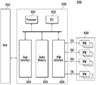
102 : 호스트
110 : 메모리 시스템
130 : 컨트롤러
132 : 호스트 인터페이스 유닛
134 : 프로세서
138 : 에러 정정 코드 유닛
140 : 파워 관리 유닛
142 : 낸드 플래시 컨트롤러
144 : 메모리
150 : 메모리 장치
Claims (20)
- 데이터들이 저장되는 복수의 메모리 블록들을 포함하는 메모리 장치; 및
상기 데이터들의 LBA(logical block address) 따라 복수의 스팟 엔트리들을 포함하는 스팟 테이블을 구성하고, 스팟 테이블을 최저사용빈도 알고리즘을 이용하여 관리하기 위한 컨트롤러를 포함하는 메모리 시스템.
- 제 1 항에 있어서,
상기 컨트롤러는 상기 스팟 테이블을 저장하기 위한 메모리; 및
상기 메모리에 저장된 스팟 테이블을 상기 최저사용빈도 알고리즘에 따라 관리하기 위한 프로세서를 포함하는 메모리 시스템.
- 제 2 항에 있어서,
상기 복수의 스팟 엔트리들 각각은 서로 상이한 스팟 카운트에 대응하는 메모리 시스템.
- 제 3 항에 있어서,
상기 스팟 테이블은 헤드 엔트리 및 테일 엔트리를 포함하는 상기 복수의 스팟 엔트리들로 구성되는 메모리 시스템.
- 제 4 항에 있어서,
상기 프로세서는 상기 호스트의 요청에 의한 제반 동작에 의해 새로운 스팟 엔트리가 생성되면, 상기 새로운 스팟 엔트리를 상기 헤드 엔트리로 지정하고, 기존의 상기 복수의 스팟 엔트리들은 상기 테일 엔트리 방향으로 하나씩 이동시켜 상기 스팟 테이블을 관리하는 메모리 시스템.
- 제 5 항에 있어서,
상기 프로세서는 상기 새로운 스팟 엔트리가 생성되면, 기존의 상기 테일 엔트리를 삭제하는 메모리 시스템.
- 제 4 항에 있어서,
상기 프로세서는 상기 호스트의 요청에 의한 상기 제반 동작에 의해 상기 복수의 스팟 엔트리들 중 선택된 스팟 엔트리의 리드 동작이 수행되면, 상기 선택된 스팟 엔트리의 상기 스팟 카운트 값을 1 상승시켜 상기 헤드 엔트리 방향으로 이동시키는 메모리 시스템.
- 제 7 항에 있어서,
상기 프로세서는 상기 선택된 스팟 엔트리와 동일한 스팟 카운트 값을 갖던 기존 스팟 엔트리의 스팟 카운트 값을 1 감소시켜 상기 테일 엔트리 방향으로 이동시키는 메모리 시스템.
- 제 3 항에 있어서,
상기 컨트롤러는 상기 복수의 스팟 엔트리들의 상기 스팟 카운트 값을 스캔하여 임계값보다 높은 스팟 카운트 값을 갖는 스팟 엔트리를 실제 스팟으로 등록하는 메모리 시스템.
- 제 9 항에 있어서,
상기 컨트롤러는 상기 실제 스팟이 검출되면, 상기 실제 스팟에 대응하는 데이터들에 대한 리드 리클레임 동작을 수행하도록 상기 메모리 장치를 제어하는 메모리 시스템.
- 데이터들이 저장되는 복수의 메모리 블록들을 포함하는 메모리 장치;
상기 데이터들의 LBA(logical block address) 따라 복수의 스팟 엔트리들을 포함하는 스팟 테이블을 구성하고, 스팟 테이블을 최저사용빈도 알고리즘을 이용하여 관리하기 위한 프로세서; 및
상기 스팟 테이블을 저장하기 위한 메모리를 포함하며,
상기 프로세서는 상기 최저사용빈도 알고리즘에 따라 상기 복수의 스팟 엔트리들 중 사용빈도가 낮은 스팟 엔트리는 삭제하는 메모리 시스템.
- 제 11 항에 있어서,
상기 복수의 스팟 엔트리들 각각은 서로 상이한 스팟 카운트를 가지며,
상기 프로세서는 상기 스팟 카운트에 따라 상기 복수의 스팟 엔트리들 중 사용빈도가 낮은 스팟 엔트리를 검출하여 삭제하는 메모리 시스템.
- 제 11 항에 있어서,
상기 스팟 테이블은 헤드 엔트리 및 테일 엔트리를 포함하는 상기 복수의 스팟 엔트리들로 구성되며,
상기 프로세서는 상기 호스트의 요청에 의한 제반 동작에 의해 새로운 스팟 엔트리가 생성되면, 상기 새로운 스팟 엔트리를 상기 헤드 엔트리로 지정하고, 기존의 상기 복수의 스팟 엔트리들은 상기 테일 엔트리 방향으로 하나씩 이동시켜 상기 스팟 테이블을 관리하는 메모리 시스템.
- 제 13 항에 있어서,
상기 프로세서는 상기 새로운 스팟 엔트리가 생성되면, 기존의 상기 테일 엔트리를 삭제하는 메모리 시스템.
- 제 13 항에 있어서,
상기 프로세서는 상기 호스트의 요청에 의한 상기 제반 동작에 의해 상기 복수의 스팟 엔트리들 중 선택된 스팟 엔트리의 리드 동작이 수행되면, 상기 선택된 스팟 엔트리의 상기 스팟 카운트 값을 1 상승시켜 상기 헤드 엔트리 방향으로 이동시키는 메모리 시스템.
- 제 15 항에 있어서,
상기 프로세서는 상기 선택된 스팟 엔트리와 동일한 스팟 카운트 값을 갖던 기존 스팟 엔트리의 스팟 카운트 값을 1 감소시켜 상기 테일 엔트리 방향으로 이동시키는 메모리 시스템.
- 데이터들의 LBA(logical block address) 따라 복수의 스팟 엔트리들을 포함하는 스팟 테이블을 구성하는 단계;
호스트의 요청에 의한 제반 동작에 의해 새로운 스팟 엔트리가 생성되면, 상기 새로운 스팟 엔트리를 상기 복수의 스팟 엔트리에 포함시키고, 상기 복수의 스팟 엔트리 중 테일 엔트리를 삭제하는 단계; 및
상기 호스트의 요청에 의해 상기 복수의 스팟 엔트리 중 선택된 스팟 엔트리의 사용 빈도수가 증가할 경우 상기 선택된 스팟 엔트리를 상기 복수의 스팟 엔트리 중 헤드 엔트리 방향으로 이동시키는 단계를 포함하는 메모리 시스템의 동작 방법.
- 제 17 항에 있어서,
상기 복수의 스팟 엔트리들 각각은 서로 상이한 스팟 카운트 값을 갖는 메모리 시스템의 동작 방법.
- 상기 헤드 엔트리는 가장 높은 상기 스팟 카운트 값을 갖고, 상기 테일 엔트리는 가낭 낮은 상기 스팟 카운트 값을 갖는 메모리 시스템의 동작 방법.
- 상기 복수의 스팟 엔트리들 중 상기 스팟 카운트 값이 임계값 보다 높은 스팟 엔트리는 실제 스팟으로 등록되며, 실제 스팟에 대응하는 상기 LBA를 갖는 데이터들을 리드 리클레임 동작이 수행되는 메모리 시스템의 동작 방법.
Priority Applications (2)
| Application Number | Priority Date | Filing Date | Title |
|---|---|---|---|
| KR1020170100297A KR102377054B1 (ko) | 2017-08-08 | 2017-08-08 | 메모리 시스템 및 그의 동작방법 |
| US15/944,929 US10768821B2 (en) | 2017-08-08 | 2018-04-04 | Memory system and method of operating the same |
Applications Claiming Priority (1)
| Application Number | Priority Date | Filing Date | Title |
|---|---|---|---|
| KR1020170100297A KR102377054B1 (ko) | 2017-08-08 | 2017-08-08 | 메모리 시스템 및 그의 동작방법 |
Publications (2)
| Publication Number | Publication Date |
|---|---|
| KR20190016632A true KR20190016632A (ko) | 2019-02-19 |
| KR102377054B1 KR102377054B1 (ko) | 2022-03-23 |
Family
ID=65275303
Family Applications (1)
| Application Number | Title | Priority Date | Filing Date |
|---|---|---|---|
| KR1020170100297A Active KR102377054B1 (ko) | 2017-08-08 | 2017-08-08 | 메모리 시스템 및 그의 동작방법 |
Country Status (2)
| Country | Link |
|---|---|
| US (1) | US10768821B2 (ko) |
| KR (1) | KR102377054B1 (ko) |
Citations (2)
| Publication number | Priority date | Publication date | Assignee | Title |
|---|---|---|---|---|
| US5043885A (en) * | 1989-08-08 | 1991-08-27 | International Business Machines Corporation | Data cache using dynamic frequency based replacement and boundary criteria |
| US20150301934A1 (en) * | 2014-04-21 | 2015-10-22 | Lsi Corporation | Flash-based data storage with dual map-based serialization |
Family Cites Families (4)
| Publication number | Priority date | Publication date | Assignee | Title |
|---|---|---|---|---|
| US8874867B2 (en) | 2008-11-21 | 2014-10-28 | Lsi Corporation | Identification and containment of performance hot-spots in virtual volumes |
| WO2010138628A1 (en) * | 2009-05-28 | 2010-12-02 | Marvell World Trade Ltd. | Metadata management for virtual volumes |
| TWI490869B (zh) * | 2010-08-13 | 2015-07-01 | Mstar Semiconductor Inc | 應用於快閃記憶體的方法與相關的控制器 |
| US9753853B2 (en) | 2014-10-09 | 2017-09-05 | Netapp, Inc. | Methods and systems for cache management in storage systems |
-
2017
- 2017-08-08 KR KR1020170100297A patent/KR102377054B1/ko active Active
-
2018
- 2018-04-04 US US15/944,929 patent/US10768821B2/en active Active
Patent Citations (2)
| Publication number | Priority date | Publication date | Assignee | Title |
|---|---|---|---|---|
| US5043885A (en) * | 1989-08-08 | 1991-08-27 | International Business Machines Corporation | Data cache using dynamic frequency based replacement and boundary criteria |
| US20150301934A1 (en) * | 2014-04-21 | 2015-10-22 | Lsi Corporation | Flash-based data storage with dual map-based serialization |
Also Published As
| Publication number | Publication date |
|---|---|
| US20190050152A1 (en) | 2019-02-14 |
| US10768821B2 (en) | 2020-09-08 |
| KR102377054B1 (ko) | 2022-03-23 |
Similar Documents
| Publication | Publication Date | Title |
|---|---|---|
| KR102791637B1 (ko) | 메모리 시스템 및 메모리 시스템의 동작 방법 | |
| KR102708642B1 (ko) | 메모리 시스템 및 메모리 시스템의 동작방법 | |
| KR102612918B1 (ko) | 컨트롤러 및 컨트롤러의 동작방법 | |
| KR20180006164A (ko) | 메모리 시스템 및 메모리 시스템의 동작 방법 | |
| KR20180039785A (ko) | 메모리 시스템 및 메모리 시스템의 동작방법 | |
| US20180373629A1 (en) | Memory system and operating method thereof | |
| KR20180030319A (ko) | 메모리 시스템 및 메모리 시스템의 동작방법 | |
| KR20180079584A (ko) | 컨트롤러 및 컨트롤러의 동작 방법 | |
| KR20190040614A (ko) | 메모리 시스템 및 그의 동작방법 | |
| KR20180005858A (ko) | 메모리 시스템 및 메모리 시스템의 동작 방법 | |
| KR102844275B1 (ko) | 메모리 시스템 및 메모리 시스템의 동작 방법 | |
| KR102415875B1 (ko) | 메모리 시스템 및 메모리 시스템의 동작 방법 | |
| KR20190042970A (ko) | 메모리 시스템 및 그의 동작방법 | |
| KR20180135188A (ko) | 메모리 시스템 및 메모리 시스템의 동작 방법 | |
| KR20200008273A (ko) | 메모리 시스템 및 메모리 시스템의 동작방법 | |
| KR20180027806A (ko) | 컨트롤러, 메모리 시스템 및 그의 동작 방법 | |
| KR20180008966A (ko) | 메모리 시스템 및 메모리 시스템의 동작 방법 | |
| KR20180076425A (ko) | 컨트롤러 및 컨트롤러의 동작 방법 | |
| KR102887870B1 (ko) | 메모리 시스템의 동작 방법 및 장치 | |
| KR20190001300A (ko) | 컨트롤러 및 메모리 시스템 및 메모리 시스템의 동작 방법 | |
| KR20180088180A (ko) | 컨트롤러 및 컨트롤러의 동작 방법 | |
| KR20190128284A (ko) | 메모리 시스템 및 메모리 시스템의 동작방법 | |
| KR20190068197A (ko) | 메모리 시스템 및 메모리 시스템의 동작방법 | |
| KR20190069806A (ko) | 메모리 시스템 및 메모리 시스템의 동작 방법 | |
| KR20180050860A (ko) | 데이터 처리 시스템 및 데이터 처리 시스템의 동작방법 |
Legal Events
| Date | Code | Title | Description |
|---|---|---|---|
| PA0109 | Patent application |
Patent event code: PA01091R01D Comment text: Patent Application Patent event date: 20170808 |
|
| PG1501 | Laying open of application | ||
| PA0201 | Request for examination |
Patent event code: PA02012R01D Patent event date: 20200807 Comment text: Request for Examination of Application Patent event code: PA02011R01I Patent event date: 20170808 Comment text: Patent Application |
|
| E902 | Notification of reason for refusal | ||
| PE0902 | Notice of grounds for rejection |
Comment text: Notification of reason for refusal Patent event date: 20210907 Patent event code: PE09021S01D |
|
| E701 | Decision to grant or registration of patent right | ||
| PE0701 | Decision of registration |
Patent event code: PE07011S01D Comment text: Decision to Grant Registration Patent event date: 20220302 |
|
| GRNT | Written decision to grant | ||
| PR0701 | Registration of establishment |
Comment text: Registration of Establishment Patent event date: 20220316 Patent event code: PR07011E01D |
|
| PR1002 | Payment of registration fee |
Payment date: 20220317 End annual number: 3 Start annual number: 1 |
|
| PG1601 | Publication of registration | ||
| PR1001 | Payment of annual fee |
Payment date: 20250225 Start annual number: 4 End annual number: 4 |