KR20190016632A - Memory system and operation method for the same - Google Patents
Memory system and operation method for the same Download PDFInfo
- Publication number
- KR20190016632A KR20190016632A KR1020170100297A KR20170100297A KR20190016632A KR 20190016632 A KR20190016632 A KR 20190016632A KR 1020170100297 A KR1020170100297 A KR 1020170100297A KR 20170100297 A KR20170100297 A KR 20170100297A KR 20190016632 A KR20190016632 A KR 20190016632A
- Authority
- KR
- South Korea
- Prior art keywords
- spot
- entry
- memory
- entries
- data
- Prior art date
- Legal status (The legal status is an assumption and is not a legal conclusion. Google has not performed a legal analysis and makes no representation as to the accuracy of the status listed.)
- Granted
Links
Images


Classifications
-
- G—PHYSICS
- G06—COMPUTING OR CALCULATING; COUNTING
- G06F—ELECTRIC DIGITAL DATA PROCESSING
- G06F13/00—Interconnection of, or transfer of information or other signals between, memories, input/output devices or central processing units
- G06F13/14—Handling requests for interconnection or transfer
- G06F13/16—Handling requests for interconnection or transfer for access to memory bus
- G06F13/1668—Details of memory controller
-
- G—PHYSICS
- G06—COMPUTING OR CALCULATING; COUNTING
- G06F—ELECTRIC DIGITAL DATA PROCESSING
- G06F3/00—Input arrangements for transferring data to be processed into a form capable of being handled by the computer; Output arrangements for transferring data from processing unit to output unit, e.g. interface arrangements
- G06F3/06—Digital input from, or digital output to, record carriers, e.g. RAID, emulated record carriers or networked record carriers
- G06F3/0601—Interfaces specially adapted for storage systems
- G06F3/0602—Interfaces specially adapted for storage systems specifically adapted to achieve a particular effect
- G06F3/0608—Saving storage space on storage systems
-
- G—PHYSICS
- G06—COMPUTING OR CALCULATING; COUNTING
- G06F—ELECTRIC DIGITAL DATA PROCESSING
- G06F12/00—Accessing, addressing or allocating within memory systems or architectures
- G06F12/02—Addressing or allocation; Relocation
- G06F12/0223—User address space allocation, e.g. contiguous or non contiguous base addressing
- G06F12/023—Free address space management
- G06F12/0238—Memory management in non-volatile memory, e.g. resistive RAM or ferroelectric memory
- G06F12/0246—Memory management in non-volatile memory, e.g. resistive RAM or ferroelectric memory in block erasable memory, e.g. flash memory
-
- G—PHYSICS
- G06—COMPUTING OR CALCULATING; COUNTING
- G06F—ELECTRIC DIGITAL DATA PROCESSING
- G06F12/00—Accessing, addressing or allocating within memory systems or architectures
- G06F12/02—Addressing or allocation; Relocation
- G06F12/0223—User address space allocation, e.g. contiguous or non contiguous base addressing
- G06F12/023—Free address space management
- G06F12/0253—Garbage collection, i.e. reclamation of unreferenced memory
-
- G—PHYSICS
- G06—COMPUTING OR CALCULATING; COUNTING
- G06F—ELECTRIC DIGITAL DATA PROCESSING
- G06F3/00—Input arrangements for transferring data to be processed into a form capable of being handled by the computer; Output arrangements for transferring data from processing unit to output unit, e.g. interface arrangements
- G06F3/06—Digital input from, or digital output to, record carriers, e.g. RAID, emulated record carriers or networked record carriers
- G06F3/0601—Interfaces specially adapted for storage systems
- G06F3/0628—Interfaces specially adapted for storage systems making use of a particular technique
- G06F3/0638—Organizing or formatting or addressing of data
- G06F3/064—Management of blocks
-
- G—PHYSICS
- G06—COMPUTING OR CALCULATING; COUNTING
- G06F—ELECTRIC DIGITAL DATA PROCESSING
- G06F3/00—Input arrangements for transferring data to be processed into a form capable of being handled by the computer; Output arrangements for transferring data from processing unit to output unit, e.g. interface arrangements
- G06F3/06—Digital input from, or digital output to, record carriers, e.g. RAID, emulated record carriers or networked record carriers
- G06F3/0601—Interfaces specially adapted for storage systems
- G06F3/0628—Interfaces specially adapted for storage systems making use of a particular technique
- G06F3/0646—Horizontal data movement in storage systems, i.e. moving data in between storage devices or systems
- G06F3/0652—Erasing, e.g. deleting, data cleaning, moving of data to a wastebasket
-
- G—PHYSICS
- G06—COMPUTING OR CALCULATING; COUNTING
- G06F—ELECTRIC DIGITAL DATA PROCESSING
- G06F3/00—Input arrangements for transferring data to be processed into a form capable of being handled by the computer; Output arrangements for transferring data from processing unit to output unit, e.g. interface arrangements
- G06F3/06—Digital input from, or digital output to, record carriers, e.g. RAID, emulated record carriers or networked record carriers
- G06F3/0601—Interfaces specially adapted for storage systems
- G06F3/0628—Interfaces specially adapted for storage systems making use of a particular technique
- G06F3/0655—Vertical data movement, i.e. input-output transfer; data movement between one or more hosts and one or more storage devices
- G06F3/0658—Controller construction arrangements
-
- G—PHYSICS
- G06—COMPUTING OR CALCULATING; COUNTING
- G06F—ELECTRIC DIGITAL DATA PROCESSING
- G06F3/00—Input arrangements for transferring data to be processed into a form capable of being handled by the computer; Output arrangements for transferring data from processing unit to output unit, e.g. interface arrangements
- G06F3/06—Digital input from, or digital output to, record carriers, e.g. RAID, emulated record carriers or networked record carriers
- G06F3/0601—Interfaces specially adapted for storage systems
- G06F3/0668—Interfaces specially adapted for storage systems adopting a particular infrastructure
- G06F3/0671—In-line storage system
- G06F3/0673—Single storage device
- G06F3/0679—Non-volatile semiconductor memory device, e.g. flash memory, one time programmable memory [OTP]
-
- G—PHYSICS
- G06—COMPUTING OR CALCULATING; COUNTING
- G06F—ELECTRIC DIGITAL DATA PROCESSING
- G06F2212/00—Indexing scheme relating to accessing, addressing or allocation within memory systems or architectures
- G06F2212/10—Providing a specific technical effect
- G06F2212/1016—Performance improvement
-
- G—PHYSICS
- G06—COMPUTING OR CALCULATING; COUNTING
- G06F—ELECTRIC DIGITAL DATA PROCESSING
- G06F2212/00—Indexing scheme relating to accessing, addressing or allocation within memory systems or architectures
- G06F2212/10—Providing a specific technical effect
- G06F2212/1041—Resource optimization
- G06F2212/1044—Space efficiency improvement
-
- G—PHYSICS
- G06—COMPUTING OR CALCULATING; COUNTING
- G06F—ELECTRIC DIGITAL DATA PROCESSING
- G06F2212/00—Indexing scheme relating to accessing, addressing or allocation within memory systems or architectures
- G06F2212/20—Employing a main memory using a specific memory technology
- G06F2212/202—Non-volatile memory
- G06F2212/2022—Flash memory
-
- G—PHYSICS
- G06—COMPUTING OR CALCULATING; COUNTING
- G06F—ELECTRIC DIGITAL DATA PROCESSING
- G06F2212/00—Indexing scheme relating to accessing, addressing or allocation within memory systems or architectures
- G06F2212/72—Details relating to flash memory management
- G06F2212/7201—Logical to physical mapping or translation of blocks or pages
-
- G—PHYSICS
- G06—COMPUTING OR CALCULATING; COUNTING
- G06F—ELECTRIC DIGITAL DATA PROCESSING
- G06F2212/00—Indexing scheme relating to accessing, addressing or allocation within memory systems or architectures
- G06F2212/72—Details relating to flash memory management
- G06F2212/7205—Cleaning, compaction, garbage collection, erase control
Landscapes
- Engineering & Computer Science (AREA)
- Theoretical Computer Science (AREA)
- Physics & Mathematics (AREA)
- General Engineering & Computer Science (AREA)
- General Physics & Mathematics (AREA)
- Human Computer Interaction (AREA)
- Techniques For Improving Reliability Of Storages (AREA)
Abstract
Description
본 발명은 비휘발성 메모리 장치를 포함하는 메모리 시스템에 관한 것으로서, 더욱 상세하게는 스팟(SPOT) 데이터를 효율적으로 관리할 수 있는 메모리 시스템 및 그 동작방법에 관한 것이다.BACKGROUND OF THE
최근 컴퓨터 환경에 대한 패러다임(paradigm)이 언제, 어디서나 컴퓨터 시스템을 사용할 수 있도록 하는 유비쿼터스 컴퓨팅(ubiquitous computing)으로 전환되고 있다. 이로 인해 휴대폰, 디지털 카메라, 노트북 컴퓨터 등과 같은 휴대용 전자 장치의 사용이 급증하고 있다. 이와 같은 휴대용 전자 장치는 일반적으로 메모리 장치를 이용하는 메모리 시스템, 다시 말해 데이터 저장 장치를 사용한다. 데이터 저장 장치는 휴대용 전자 장치의 주 기억 장치 또는 보조 기억 장치로 사용된다.Recently, a paradigm for a computer environment has been transformed into ubiquitous computing, which enables a computer system to be used whenever and wherever. As a result, the use of portable electronic devices such as mobile phones, digital cameras, and notebook computers is rapidly increasing. Such portable electronic devices typically use memory systems that use memory devices, i. E., Data storage devices. The data storage device is used as a main storage device or an auxiliary storage device of a portable electronic device.
메모리 장치를 이용한 데이터 저장 장치는 기계적인 구동부가 없어서 안정성 및 내구성이 뛰어나며, 또한 정보의 액세스 속도가 매우 빠르고 전력 소모가 적다는 장점이 있다. 이러한 장점을 갖는 메모리 시스템의 일 예로 데이터 저장 장치는 USB(Universal Serial Bus) 메모리 장치, 다양한 인터페이스를 갖는 메모리 카드, 솔리드 스테이트 드라이브(SSD: Solid State Drive) 등을 포함한다.The data storage device using the memory device is advantageous in that it has excellent stability and durability because there is no mechanical driving part, and the access speed of information is very fast and power consumption is low. As an example of a memory system having such advantages, a data storage device includes a universal serial bus (USB) memory device, a memory card having various interfaces, and a solid state drive (SSD).
본 발명의 실시 예는 메모리 시스템의 동작 시 워크 로드(work-load)에 의해 발생할 수 있는 스팟 데이터들을 효율적으로 관리하여 메모리 시스템의 신뢰성을 개선할 수 있는 메모리 시스템 및 그의 동작 방법을 제공한다.Embodiments of the present invention provide a memory system and a method of operating the same that can efficiently manage the spot data that can be generated by a work-load in the operation of the memory system to improve the reliability of the memory system.
본 발명의 실시 예에 따른 메모리 시스템은 데이터들이 저장되는 복수의 메모리 블록들을 포함하는 메모리 장치 및 상기 데이터들의 LBA(logical block address) 따라 복수의 스팟 엔트리들을 포함하는 스팟 테이블을 구성하고, 스팟 테이블을 최저사용빈도 알고리즘을 이용하여 관리하기 위한 컨트롤러를 포함한다.A memory system according to an embodiment of the present invention includes a memory device including a plurality of memory blocks in which data is stored and a spot table including a plurality of spot entries according to a logical block address (LBA) of the data, And a controller for managing using the lowest use frequency algorithm.
본 발명의 실시 예에 따른 메모리 시스템은 데이터들이 저장되는 복수의 메모리 블록들을 포함하는 메모리 장치, 상기 데이터들의 LBA(logical block address) 따라 복수의 스팟 엔트리들을 포함하는 스팟 테이블을 구성하고, 스팟 테이블을 최저사용빈도 알고리즘을 이용하여 관리하기 위한 프로세서; 및 상기 스팟 테이블을 저장하기 위한 메모리를 포함하며, 상기 프로세서는 상기 최저사용빈도 알고리즘에 따라 상기 복수의 스팟 엔트리들 중 사용빈도가 낮은 스팟 엔트리는 삭제한다.A memory system according to an embodiment of the present invention includes a memory device including a plurality of memory blocks in which data is stored, a spot table including a plurality of spot entries according to a logical block address (LBA) of the data, A processor for managing using the lowest use frequency algorithm; And a memory for storing the spot table, wherein the processor deletes spot entries having a low frequency of use among the plurality of spot entries according to the lowest use frequency algorithm.
본 발명의 실시 예에 따른 메모리 시스템의 동작 방법은 데이터들의 LBA(logical block address) 따라 복수의 스팟 엔트리들을 포함하는 스팟 테이블을 구성하는 단계와, 호스트의 요청에 의한 제반 동작에 의해 새로운 스팟 엔트리가 생성되면, 상기 새로운 스팟 엔트리를 상기 복수의 스팟 엔트리에 포함시키고, 상기 복수의 스팟 엔트리 중 테일 엔트리를 삭제하는 단계, 및 상기 호스트의 요청에 의해 상기 복수의 스팟 엔트리 중 선택된 스팟 엔트리의 사용 빈도수가 증가할 경우 상기 선택된 스팟 엔트리를 상기 복수의 스팟 엔트리 중 헤드 엔트리 방향으로 이동시키는 단계를 포함한다.A method of operating a memory system according to an embodiment of the present invention includes: constructing a spot table including a plurality of spot entries according to a logical block address (LBA) of data; The method comprising the steps of: if the new spot entry is created, including the new spot entry in the plurality of spot entries and deleting a tail entry of the plurality of spot entries; and if the frequency of use of the selected spot entry of the plurality of spot entries And moving the selected spot entry in the direction of the head entry among the plurality of spot entries.
본 기술에 따르면, 스팟 데이터들을 LBA(logical block address) 범위로 나누어 복수의 스팟 엔트리를 관리하되, 새로운 스팟 엔트리가 발생하거나 기존 스팟 엔트리의 리드 횟수가 증가할 경우 스팟 테이블을 최저사용빈도 알고리즘에 따라 관리함으로써, 효율적으로 스팟 데이터들을 관리할 수 있다.According to the present invention, a plurality of spot entries are managed by dividing spot data into a logical block address (LBA) range. When a new spot entry occurs or a lead number of existing spot entries increases, the spot table is updated according to the minimum use frequency algorithm By managing the spot data, the spot data can be efficiently managed.
도 1은 본 발명의 실시 예에 따른 메모리 시스템을 포함하는 데이터 처리 시스템의 일 예를 도시한 도면이다.
도 2는 본 발명의 실시 예에 따른 메모리 시스템에서 메모리 장치의 일 예를 도시한 도면이다.
도 3은 본 발명의 실시 예에 따른 메모리 장치에서 메모리 블록들의 메모리 셀 어레이 회로를 도시한 도면이다.
도 4는 본 발명의 실시 예에 따른 메모리 시스템에서 메모리 장치 구조를 도시한 도면이다.
도 5는 본 발명의 실시 예에 따른 스팟 테이블을 설명하기 위한 구성도이다.
도 6 및 도 7은 본 발명의 실시 예에 따른 스팟 엔트리를 관리하는 방법을 설명하기 위한 구성도이다.
도 8은 본 발명의 실시 예에 따른 스팟 엔트리에 따라 메모리 시스템이 동작하는 방법을 설명하기 위한 순서도이다.
도 9 내지 도 12는 본 발명의 실시 예에 따른 메모리 시스템을 포함하는 데이터 처리 시스템의 다른 일 예들을 도시한 도면이다.1 is a diagram illustrating an example of a data processing system including a memory system according to an embodiment of the present invention.
2 is a diagram illustrating an example of a memory device in a memory system according to an embodiment of the present invention.
3 is a diagram illustrating a memory cell array circuit of memory blocks in a memory device according to an embodiment of the present invention.
4 is a diagram illustrating a memory device structure in a memory system according to an embodiment of the present invention.
5 is a block diagram illustrating a spot table according to an embodiment of the present invention.
6 and 7 are block diagrams for explaining a method of managing a spot entry according to an embodiment of the present invention.
8 is a flowchart illustrating a method of operating a memory system according to a spot entry according to an embodiment of the present invention.
9 through 12 are diagrams illustrating other examples of a data processing system including a memory system according to an embodiment of the present invention.
본 발명의 이점 및 특징, 그리고 그것을 달성하는 방법은 첨부되는 도면과 함께 상세하게 후술되어 있는 실시 예들을 통해 설명될 것이다. 그러나 본 발명은 여기에서 설명되는 실시 예들에 한정되지 않고 다른 형태로 구체화될 수도 있다. 단지, 본 실시 예들은 본 발명이 속하는 기술분야에서 통상의 지식을 가진 자에게 본 발명의 기술적 사상을 용이하게 실시할 수 있을 정도로 상세히 설명하기 위하여 제공되는 것이다.BRIEF DESCRIPTION OF THE DRAWINGS The advantages and features of the present invention, and how to accomplish it, will be described with reference to the embodiments described in detail below with reference to the accompanying drawings. However, the present invention is not limited to the embodiments described herein but may be embodied in other forms. The embodiments are provided so that those skilled in the art can easily carry out the technical idea of the present invention to those skilled in the art.
명세서 전체에서, 어떤 부분이 다른 부분과 "연결"되어 있다고 할 때, 이는 "직접적으로 연결"되어 있는 경우뿐 아니라, 그 중간에 다른 소자를 사이에 두고 "간접적으로 연결"되어 있는 경우도 포함한다. 명세서 전체에서, 어떤 부분이 어떤 구성요소를 "포함"한다고 할 때, 이는 특별히 반대되는 기재가 없는 한 다른 구성요소를 제외하는 것이 아니라 다른 구성요소를 더 포함할 수 있는 것을 의미한다.Throughout the specification, when a part is referred to as being "connected" to another part, it includes not only "directly connected" but also "indirectly connected" . Throughout the specification, when an element is referred to as "comprising ", it means that it can include other elements as well, without excluding other elements unless specifically stated otherwise.
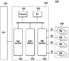
도 1은 본 발명의 실시 예에 따른 메모리 시스템을 포함하는 데이터 처리 시스템의 일 예를 도시한 도면이다.1 is a diagram illustrating an example of a data processing system including a memory system according to an embodiment of the present invention.
도 1을 참조하면, 데이터 처리 시스템(100)은 호스트(Host)(102) 및 메모리 시스템(110)을 포함한다.Referring to FIG. 1, a
호스트(102)는 휴대폰, MP3 플레이어, 랩탑 컴퓨터 등과 같은 휴대용 전자 장치들, 또는 데스크탑 컴퓨터, 게임기, TV, 프로젝터 등과 같은 전자 장치들을 포함한다.The
또한, 메모리 시스템(110)은 호스트(102)의 요청에 응답하여 동작하며, 특히 호스트(102)에 의해서 액세스되는 데이터를 저장한다. 다시 말해, 메모리 시스템(110)은 호스트(102)의 주 기억 장치 또는 보조 기억 장치로 사용될 수 있다. 여기서, 메모리 시스템(110)은 호스트(102)와 연결되는 호스트 인터페이스 프로토콜에 따라, 다양한 종류의 저장 장치들 중 어느 하나로 구현될 수 있다. 예를 들면, 메모리 시스템(110)은 솔리드 스테이트 드라이브(SSD: Solid State Drive), MMC, eMMC(embedded MMC), RS-MMC(Reduced Size MMC), micro-MMC 형태의 멀티 미디어 카드(MMC: Multi Media Card), SD, mini-SD, micro-SD 형태의 시큐어 디지털(SD: Secure Digital) 카드, USB(Universal Storage Bus) 저장 장치, UFS(Universal Flash Storage) 장치, CF(Compact Flash) 카드, 스마트 미디어(Smart Media) 카드, 메모리 스틱(Memory Stick) 등과 같은 다양한 종류의 저장 장치들 중 어느 하나로 구현될 수 있다.The
아울러, 메모리 시스템(110)을 구현하는 저장 장치들은 DRAM(Dynamic Random Access Memory), SRAM(Static RAM) 등과 같은 휘발성 메모리 장치와 ROM(Read Only Memory), MROM(Mask ROM), PROM(Programmable ROM), EPROM(Erasable ROM), EEPROM(Electrically Erasable ROM), FRAM(Ferromagnetic ROM), PRAM(Phase change RAM), MRAM(Magnetic RAM), RRAM(Resistive RAM), 플래시 메모리 등과 같은 비휘발성 메모리 장치로 구현될 수 있다.In addition, the storage devices implementing the
그리고, 메모리 시스템(110)은 호스트(102)에 의해서 액세스되는 데이터를 저장하는 메모리 장치(150), 및 메모리 장치(150)로의 데이터 저장을 제어하는 컨트롤러(130)를 포함한다.The
여기서, 컨트롤러(130) 및 메모리 장치(150)는 하나의 반도체 장치로 집적될 수 있다. 일 예로, 컨트롤러(130) 및 메모리 장치(150)는 하나의 반도체 장치로 집적되어 SSD를 구성할 수 있다. 메모리 시스템(110)이 SSD로 이용되는 경우, 메모리 시스템(110)에 연결되는 호스트(102)의 동작 속도는 획기적으로 개선될 수 있다.Here, the
컨트롤러(130) 및 메모리 장치(150)는 하나의 반도체 장치로 집적되어, 메모리 카드를 구성할 수 있다. 예를 들면, 컨트롤러(130) 및 메모리 장치(150)는 하나의 반도체 장치로 집적되어, PC 카드(PCMCIA: Personal Computer Memory Card International Association), 컴팩트 플래시 카드(CF), 스마트 미디어 카드(SM, SMC), 메모리 스틱, 멀티미디어 카드(MMC, RS-MMC, MMCmicro), SD 카드(SD, miniSD, microSD, SDHC), 유니버설 플래시 기억 장치(UFS) 등과 같은 메모리 카드를 구성할 수 있다.The
또 다른 일 예로, 메모리 시스템(110)은 컴퓨터, UMPC(Ultra Mobile PC), 워크스테이션, 넷북(net-book), PDA(Personal Digital Assistants), 포터블(portable) 컴퓨터, 웹 타블렛(web tablet), 태블릿 컴퓨터(tablet computer), 무선 전화기(wireless phone), 모바일 폰(mobile phone), 스마트폰(smart phone), e-북(e-book), PMP(portable multimedia player), 휴대용 게임기, 네비게이션(navigation) 장치, 블랙박스(black box), 디지털 카메라(digital camera), DMB(Digital Multimedia Broadcasting) 재생기, 3차원 텔레비전(3-dimensional television), 스마트 텔레비전(smart television), 디지털 음성 녹음기(digital audio recorder), 디지털 음성 재생기(digital audio player), 디지털 영상 녹화기(digital picture recorder), 디지털 영상 재생기(digital picture player), 디지털 동영상 녹화기(digital video recorder), 디지털 동영상 재생기(digital video player), 데이터 센터를 구성하는 스토리지, 정보를 무선 환경에서 송수신할 수 있는 장치, 홈 네트워크를 구성하는 다양한 전자 장치들 중 하나, 컴퓨터 네트워크를 구성하는 다양한 전자 장치들 중 하나, 텔레매틱스 네트워크를 구성하는 다양한 전자 장치들 중 하나, RFID(radio frequency identification) 장치, 또는 컴퓨팅 시스템을 구성하는 다양한 구성 요소들 중 하나 등을 구성할 수 있다.As another example, the
한편, 메모리 시스템(110)의 메모리 장치(150)는 전원이 공급되지 않아도 저장된 데이터를 유지할 수 있으며, 특히 라이트(write) 동작을 통해 호스트(102)로부터 제공된 데이터를 저장하고, 리드(read) 동작을 통해 저장된 데이터를 호스트(102)로 제공한다.Meanwhile, the
메모리 장치(150)는 복수의 메모리 블록(memory block)들(152,154,156)을 포함하며, 각각의 메모리 블록들(152,154,156)은 복수의 페이지들(pages)을 포함하며, 또한 각각의 페이지들은 복수의 워드라인(Word Line)들이 연결된 복수의 메모리 셀들을 포함한다. 또한, 메모리 장치(150)는 복수의 메모리 블록들(152,154,156)이 각각 포함된 복수의 플래인들(plane)을 포함하며, 특히 복수의 플래인들이 각각 포함된 복수의 메모리 다이(memory die)들을 포함할 수 있다. 메모리 장치(150)는 비휘발성 메모리 장치, 일 예로 플래시 메모리가 될 수 있으며, 이때 플래시 메모리는 3차원(dimension) 입체 스택(stack) 구조가 될 수 있다.The
메모리 장치(150)의 구조 및 메모리 장치(150)의 3차원 입체 스택 구조에 대해서는 이하 도 2 내지 도 4에서 보다 구체적으로 설명하도록 한다.The structure of the
메모리 시스템(110)의 컨트롤러(130)는 호스트(102)로부터의 요청에 응답하여 메모리 장치(150)를 제어한다. 컨트롤러(130)는 메모리 장치(150)로부터 리드된 데이터를 호스트(102)로 제공하고, 호스트(102)로부터 제공된 데이터를 메모리 장치(150)에 저장하며, 이를 위해 컨트롤러(130)는 메모리 장치(150)의 리드, 라이트, 프로그램(program), 이레이즈(erase) 등의 동작을 제어한다.The
또한 컨트롤러(130)는 컨트롤러(130)는 워크 로드(work-load)가 특정 어드레스에 집중되는 있는 집합체 또는 집합체 그룹인 스팟(SPOT)을 관리하여 스팟에 대응하는 데이터들의 신뢰성을 개선하기 위하여 리드 리클레임(read reclaim) 동작을 수행할 수 있다. 컨트롤러(130)는 데이터들의 LBA(logical block address: 논리적 블록 어드레스) 따라 복수의 스팟 엔트리(SPOT entry)를 포함하는 테이블을 구성하고, 각 스팟 엔트리에 대응하는 LBA를 갖는 데이터들의 리드 및 라이트 횟수에 따른 스팟 엔트리의 사용빈도를 결정하고, 스팟 엔트리의 사용빈도에 따라 스팟 엔트리의 우선 순위를 재결정하여 테이블을 관리할 수 있다. 스팟 엔트리의 관리 방법에 대해서는 후술하도록 한다. In addition, the
컨트롤러(130)는 호스트 인터페이스(Host I/F) 유닛(132), 프로세서(Processor)(134), 에러 정정 코드(ECC: Error Correction Code) 유닛(138), 파워 관리 유닛(PMU: Power Management Unit)(140), 낸드 플래시 컨트롤러(NFC: NAND Flash Controller)(142), 및 메모리(Memory)(144)를 포함한다.The
호스트 인터페이스 유닛(134)은 호스트(102)의 커맨드(command) 및 데이터를 처리하며, USB(Universal Serial Bus), MMC(Multi-Media Card), PCI-E(Peripheral Component Interconnect-Express), SAS(Serial-attached SCSI), SATA(Serial Advanced Technology Attachment), PATA(Parallel Advanced Technology Attachment), SCSI(Small Computer System Interface), ESDI(Enhanced Small Disk Interface), IDE(Integrated Drive Electronics) 등과 같은 다양한 인터페이스 프로토콜들 중 적어도 하나를 통해 호스트(102)와 통신하도록 구성될 수 있다.The
ECC 유닛(138)은 메모리 장치(150)에 저장된 데이터를 리드할 경우, 메모리 장치(150)로부터 리드된 데이터에 포함되는 에러를 검출 및 정정한다. 다시 말해, ECC 유닛(138)은 메모리 장치(150)로부터 리드한 데이터에 대하여 에러 정정 디코딩을 수행한 후, 에러 정정 디코딩의 성공 여부를 판단하고 판단 결과에 따라 지시 신호를 출력하며, ECC 인코딩 과정에서 생성된 패리티(parity) 비트를 사용하여 리드된 데이터의 에러 비트를 정정할 수 있다. 이때, ECC 유닛(138)은 에러 비트 개수가 정정 가능한 에러 비트 한계치 이상 발생하면, 에러 비트를 정정할 수 없으며, 에러 비트를 정정하지 못함에 상응하는 에러 정정 실패(fail) 신호를 출력할 수 있다.The
ECC 유닛(138)은 LDPC(low density parity check) code, BCH(Bose, Chaudhri, Hocquenghem) code, turbo code, 리드-솔로몬 코드(Reed-Solomon code), convolution code, RSC(recursive systematic code), TCM(trellis-coded modulation), BCM(Block coded modulation) 등의 코디드 모듈레이션(coded modulation)을 사용하여 에러 정정을 수행할 수 있으며 이에 한정되는 것은 아니다. 또한, ECC 유닛(138)는 오류 정정을 위한 회로, 시스템 또는 장치를 모두 포함할 수 있다.The
PMU(140)는 컨트롤러(130)의 파워, 즉 컨트롤러(130)에 포함된 구성 요소들의 파워를 제공 및 관리한다.The
NFC(142)는 컨트롤러(130)가 호스트(102)로부터의 요청에 응답하여 메모리 장치(150)를 제어하기 위해, 컨트롤러(130)와 메모리 장치(150) 간의 인터페이싱을 수행하는 메모리 인터페이스로서, 메모리 장치(150)가 플래시 메모리, 특히 일 예로 메모리 장치(150)가 낸드 플래시 메모리일 경우에, 프로세서(134)의 제어에 따라 메모리 장치(150)의 제어 신호를 생성하고 데이터를 처리한다.
메모리(144)는 메모리 시스템(110) 및 컨트롤러(130)의 동작 메모리로, 메모리 시스템(110) 및 컨트롤러(130)의 구동을 위한 데이터를 저장한다. 예를 들어 컨트롤러(130)가, 메모리 장치(150)의 리드, 라이트, 프로그램, 이레이즈(erase) 등의 동작을 제어할 경우, 이러한 동작을 수행하기 위해 필요한 데이터를 메모리(144)에 저장한다.The
또한 메모리(144)는 메모리 시스템(110)의 스팟 테이블을 저장하며, 스팟 테이블에 따라 실제 스팟으로 판단된 스팟 영역에 대한 정보를 저장할 수 있다. 메모리(144)는 휘발성 메모리로 구현될 수 있으며, 정적 랜덤 액세스 메모리(SRAM: Static Random Access Memory), 또는 동적 랜덤 액세스 메모리(DRAM: Dynamic Random Access Memory) 등으로 구현될 수 있다. 또한, 메모리(144)는 전술한 바와 같이, 호스트(102)와 메모리 장치(150) 간 데이터 라이트 및 리드 등의 동작을 수행하기 위해 필요한 데이터, 및 데이터 라이트 및 리드 등의 동작 수행 시의 데이터를 저장하며, 이러한 데이터 저장을 위해, 프로그램 메모리, 데이터 메모리, 라이트 버퍼(buffer)/캐시(cache), 리드 버퍼/캐시, 맵(map) 버퍼/캐시 등을 포함한다.The
프로세서(134)는 메모리 시스템(110)의 제반 동작을 제어하며, 호스트(102)로부터의 라이트 요청 또는 리드 요청에 응답하여, 메모리 장치(150)에 대한 라이트 동작 또는 리드 동작을 제어한다. 여기서, 프로세서(134)는 메모리 시스템(110)의 제반 동작을 제어하기 위해 플래시 변환 계층(FTL: Flash Translation Layer, 이하 'FTL'이라 칭하기로 함)이라 불리는 펌웨어(firmware)를 구동한다. 또한, 프로세서(134)는 마이크로프로세서 또는 중앙 처리 장치(CPU) 등으로 구현될 수 있다.The
컨트롤러(130)는 마이크로프로세서 또는 중앙 처리 장치(CPU) 등으로 구현된 프로세서(134)를 통해, 호스트(102)로부터 요청된 동작을 메모리 장치(150)에서 수행, 다시 말해 호스트(102)로부터 수신된 커맨드에 해당하는 커맨드 동작을, 메모리 장치(150)와 수행한다. 여기서, 컨트롤러(130)는 호스트(102)로부터 수신된 커맨드에 해당하는 커맨드 동작으로 포그라운드(foreground) 동작을 수행할 수 있다.The
또한 컨트롤러(130)는 마이크로프로세서 또는 중앙 처장치(CPU) 등으로 구현된 프로세서(134)를 통해, 메모리 장치(150)에 대한 백그라운드(background) 동작을 수행할 수도 있다. 여기서, 메모리 장치(150)에 대한 백그라운드 동작은 메모리 장치(150)의 메모리 블록들(152,154,156)에서 임의의 메모리 블록에 저장된 데이터를 다른 임의의 메모리 블록으로 카피(copy)하여 처리하는 동작, 일 예로 가비지 컬렉션(Garbage Collection) 동작, 메모리 장치(150)의 메모리 블록들(152,154,156) 간 또는 메모리 블록들(152,154,156)에 저장된 데이터 간을 스왑(swap)하여 처리하는 동작, 일 예로 웨어 레벨링(Wear Leveling) 동작, 컨트롤러(130)에 저장된 맵 데이터를 메모리 장치(150)의 메모리 블록들(152,154,156)로 저장하는 동작, 일 예로 맵 플러시(map flush) 동작, 또는 메모리 장치(150)에 대한 배드 관리(bad management)하는 동작, 일 예로 메모리 장치(150)에 포함된 복수의 메모리 블록들(152,154,156)에서 배드 블록을 확인하여 처리하는 배드 블록 관리(bad block management) 동작 등을 포함한다. The
특히, 본 발명의 실시 예에 따른 메모리 시스템(110)에서는 프로세서(134)를 통해 스팟을 관리하여 스팟에 대응하는 데이터들의 신뢰성을 개선하기 위하여 리드 리클레임(read reclaim) 동작을 수행하도록 메모리 장치(150)를 제어할 수 있다.In particular, in the
도 2는 본 발명의 실시 예에 따른 메모리 시스템에서 메모리 장치의 일 예를 도시한 도면이다. 도 3은 본 발명의 실시 예에 따른 메모리 장치에서 메모리 블록들의 메모리 셀 어레이 회로를 도시한 도면이다. 도 4는 본 발명의 실시 예에 따른 메모리 시스템에서 메모리 장치 구조를 도시한 도면이다.2 is a diagram illustrating an example of a memory device in a memory system according to an embodiment of the present invention. 3 is a diagram illustrating a memory cell array circuit of memory blocks in a memory device according to an embodiment of the present invention. 4 is a diagram illustrating a memory device structure in a memory system according to an embodiment of the present invention.
도 2 내지 도 4를 참조하여 본 발명의 실시 예에 따른 메모리 시스템에서의 메모리 장치에 대해서 보다 구체적으로 설명하면 다음과 같다.The memory device in the memory system according to the embodiment of the present invention will be described in more detail with reference to FIGS. 2 to 4. FIG.
도 2를 참조하면, 메모리 장치(150)는 복수의 메모리 블록들, 예를 들어 블록0(BLK0)(210), 블록1(BLK1)(220), 블록2(BLK2)(230), 및 블록N-1(BLKN-1)(240)을 포함하며, 각각의 블록들(210,220,230,240)은 복수의 페이지들(Pages), 예컨대 2M개의 페이지들(2MPages)을 포함한다. 여기서, 설명의 편의를 위해 복수의 메모리 블록들이 각각 2M개의 페이지들을 포함하는 것을 일 예로 하여 설명하지만, 복수의 메모리 블록들은 각각 M개의 페이지들을 포함할 수도 있다. 각각의 페이지들은 복수의 워드라인(Word Line)들이 연결된 복수의 메모리 셀들을 포함한다.2, the
또한, 메모리 장치(150)는 복수의 메모리 블록들을, 하나의 메모리 셀에 저장할 수 있는 데이터의 비트의 수에 따라, 단일 레벨 셀(SLC: Single Level Cell) 메모리 블록 및 멀티 레벨 셀(MLC: Multi Level Cell) 메모리 블록 등으로 포함할 수 있다. 여기서, SLC 메모리 블록은 하나의 메모리 셀에 1 비트 데이터를 저장하는 메모리 셀들에 의해 구현된 복수의 페이지들을 포함하며, 데이터 연산 성능이 빠르며 내구성이 높다. MLC 메모리 블록은 하나의 메모리 셀에 멀티 비트 데이터(예를 들면, 2 비트 이상)를 저장하는 메모리 셀들에 의해 구현된 복수의 페이지들을 포함하며, SLC 메모리 블록보다 큰 데이터 저장 공간을 가질 수 있다. 하나의 메모리 셀에 3 또는 4 비트 데이터를 저장할 수 있는 메모리 셀들에 의해 구현된 복수의 페이지들을 포함하는 MLC 메모리 블록을 트리플 레벨 셀(TLC: Triple Level Cell) 또는 쿼드 레벨 셀(QLC: Quad Level Cell) 메모리 블록으로 구분할 수도 있다.In addition, the
각각의 블록들(210,220,230,240)은 라이트 동작을 통해 호스트(102)로부터 제공된 데이터를 저장하고, 리드 동작을 통해 저장된 데이터를 호스트(102)에게 제공한다.Each of the
도 3을 참조하면, 메모리 시스템(110)의 메모리 장치(150)에 포함된 복수의 메모리 블록들(152,154,156)에서 각 메모리 블록(330)은 메모리 셀 어레이로 구현되어 비트라인들(BL0 to BLm-1)에 각각 연결된 복수의 셀 스트링들(340)을 포함할 수 있다. 각 열(column)의 셀 스트링(340)은 적어도 하나의 드레인 선택 트랜지스터(DST)와, 적어도 하나의 소스 선택 트랜지스터(SST)를 포함할 수 있다. 선택 트랜지스터들(DST, SST) 사이에는 복수 개의 메모리 셀들(MC0 to MCn-1)이 직렬로 연결될 수 있다. 각각의 메모리 셀(MC0 to MCn-1)은 셀 당 복수의 비트들의 데이터 정보를 저장하는 MLC로 구성될 수 있다. 셀 스트링들(340)은 대응하는 비트라인들(BL0 to BLm-1)에 각각 전기적으로 연결될 수 있다.3, in a plurality of memory blocks 152, 154, 156 included in a
도 3은 낸드 플래시 메모리 셀로 구성된 각 메모리 블록(330)을 일 예로 도시하고 있으나, 본 발명의 실시 예에 따른 메모리 장치(150)에 포함된 복수의 메모리 블록(152,154,156)은 낸드 플래시 메모리에만 국한되는 것은 아니라 노어 플래시 메모리(NOR-type Flash memory), 적어도 두 종류 이상의 메모리 셀들이 혼합된 하이브리드 플래시 메모리, 메모리 칩 내에 컨트롤러가 내장된 One-NAND 플래시 메모리 등으로도 구현될 수 있다. 아울러, 본 발명의 실시 예에 따른 메모리 장치(150)는 전하 저장층이 전도성 부유 게이트로 구성된 플래시 메모리 장치는 물론, 전하 저장층이 절연막으로 구성된 차지 트랩형 플래시(Charge Trap Flash; CTF) 메모리 장치 등으로도 구현될 수 있다.Although FIG. 3 illustrates each
메모리 장치(150)의 전압 공급부(310)는 동작 모드에 따라서 각각의 워드라인들로 공급될 워드라인 전압들(예를 들면, 프로그램 전압, 리드 전압, 패스 전압 등)과, 메모리 셀들이 형성된 벌크(예를 들면, 웰 영역)로 공급될 전압을 제공할 수 있으며, 이때 전압 공급부(310)의 전압 발생 동작은 제어 회로(도시하지 않음)의 제어에 의해 수행될 수 있다. 또한, 전압 공급부(310)는 다수의 리드 데이터를 생성하기 위해 복수의 가변 리드 전압들을 생성할 수 있으며, 제어 회로의 제어에 응답하여 메모리 셀 어레이의 메모리 블록들(또는 섹터들) 중 하나를 선택하고, 선택된 메모리 블록의 워드라인들 중 하나를 선택할 수 있으며, 워드라인 전압을 선택된 워드라인 및 비선택된 워드라인들로 각각 제공할 수 있다.The
메모리 장치(150)의 리드/라이트(read/write) 회로(320)는 제어 회로에 의해서 제어되며, 동작 모드에 따라 감지 증폭기(sense amplifier)로서 또는 라이트 드라이버(write driver)로서 동작할 수 있다. 예를 들면, 검증/정상 리드 동작의 경우 리드/라이트 회로(320)는 메모리 셀 어레이로부터 데이터를 리드하기 위한 감지 증폭기로서 동작할 수 있다. 또한, 프로그램 동작의 경우 리드/라이트 회로(320)는 메모리 셀 어레이에 저장될 데이터에 따라 비트라인들을 구동하는 라이트 드라이버로서 동작할 수 있다. 리드/라이트 회로(320)는 프로그램 동작 시 셀 어레이에 라이트될 데이터를 버퍼(미도시)로부터 수신하고, 입력된 데이터에 따라 비트라인들을 구동할 수 있다. 이를 위해, 리드/라이트 회로(320)는 열(column)들(또는 비트라인들) 또는 열쌍(column pair)(또는 비트라인 쌍들)에 각각 대응되는 복수 개의 페이지 버퍼들(PB)(322,324,326)을 포함할 수 있으며, 각각의 페이지 버퍼(page buffer)(322,324,326)에는 복수의 래치들(도시하지 않음)이 포함될 수 있다.The read /
또한, 메모리 장치(150)는 2차원 또는 3차원의 메모리 장치로 구현될 수 있으며, 특히 도 4에 도시한 바와 같이 3차원 입체 스택 구조의 비휘발성 메모리 장치로 구현될 수 있으며, 3차원 구조로 구현될 경우 복수의 메모리 블록들(BLK0 to BLKN-1)을 포함할 수 있다. 여기서, 도 4는 도 1에 도시한 메모리 장치(150)의 메모리 블록들(152,154,156)을 보여주는 블록도로서, 각각의 메모리 블록들(152,154,156)은 3차원 구조(또는 수직 구조)로 구현될 수 있다. 예를 들면, 각각의 메모리 블록들(152,154,156)은 제1방향 내지 제3방향들, 예컨대 x-축 방향, y-축 방향, 및 z-축 방향을 따라 신장된 구조물들을 포함하여, 3차원 구조로 구현될 수 있다.In addition, the
도 5는 본 발명의 실시 예에 따른 스팟 테이블을 설명하기 위한 구성도이다.5 is a block diagram illustrating a spot table according to an embodiment of the present invention.
도 5를 참조하면, 도 1에 도시된 프로세서(134)를 통해 스팟 테이블(SPOT Table)을 구성할 수 있다. 스팟 테이블(SPOT Table)은 복수의 스팟 엔트리 인덱스들(SPOT ENTRY 0 내지 SPOT ENTRY M)을 포함하여 구성된다. 일 예로 스팟 테이블(SPOT Table)은 데이터들의 LBA(logical block address) 범위를 기준으로 하여 복수의 스팟 엔트리 인덱스들을 구성할 수 있다. 예를 들어 LBA(0~N)에 대응하는 스팟 데이터들은 스팟 엔트리 인덱스(SPOT ENTRY 0)로 정의하고, LBA(N+1~2N)에 대응하는 스팟 데이터들은 스팟 엔트리 인덱스(SPOT ENTRY 1)로 정의하고, LBA(2N+1~3N)에 대응하는 스팟 데이터들은 스팟 엔트리 인덱스(SPOT ENTRY 2)로 정의하고, LBA(M*N+1~(N+1)*M)에 대응하는 스팟 데이터들은 스팟 엔트리 인덱스(SPOT ENTRY M)으로 정의할 수 있다.Referring to FIG. 5, a SPOT table can be configured through the
또한 복수의 스팟 엔트리 인덱스들(SPOT ENTRY 0 내지 SPOT ENTRY M) 각각은 대응하는 스팟 카운트 값(SPOT Count)을 가질 수 있다. 예를들어, 스팟 엔트리 인덱스(SPOT ENTRY 0)는 스팟 카운트 M(SPOT Count M)을 갖고, 스팟 엔트리 인덱스(SPOT ENTRY 1)는 스팟 카운트 M(SPOT Count M-1)을 갖고, 스팟 엔트리 인덱스(SPOT ENTRY 2)는 스팟 카운트 M(SPOT Count M-2)을 갖고, 스팟 엔트리 인덱스(SPOT ENTRY M)는 스팟 카운트 M(SPOT Count 0)을 갖도록 스팟 테이블(SPOT Table)을 구성할 수 있다. 본 발명의 실시 예에서는 복수의 스팟 엔트리 인덱스들에 대응하는 스팟 카운트 값(SPOT Count)이 순차적으로 감소하도록 구성하였으나, 이에 한정되는 것은 아니며 복수의 스팟 엔트리 인덱스들에 대응하는 스팟 카운트 값(SPOT Count)이 서로 상이하도록 구성한다. 즉, 복수의 스팟 엔트리 인덱스들에 대응하는 스팟 카운트 값(SPOT Count)이 서로 중복되지 않도록 구성한다. Also, each of the plurality of spot entry indices (
상술한 스팟 테이블(SPOT Table) 구성에 따르면, LBA의 유닛 사이즈가 4KB이고 LBA의 범위가 0 내지 1000이고 처리 가능한 스팟 엔트리 수가 1000개라고 가정할 경우, 전체 4GB의 스팟 영역을 관리할 수 있으며, 이때 사용되는 스팟 테이블(SPOT Table)을 위한 메모리 용량은 스팟 엔트리의 메모리 사이즈와 카운트 값을 관리하기 위한 메모리 사이즈를 합한 메모리 용량으로 관리할 수 있다. 예를 들어 스팟 엔트리 인덱스가 헤드(head) 엔트리(2byte)와 테일(tail) 엔트리(2byte) 및 카운트 사이즈(2byte)를 포함할 경우 약 6KB의 메모리 용량으로 스팟 영역을 관리할 수 있다.According to the above-mentioned SPOT Table configuration, if the unit size of the LBA is 4 KB, the range of the LBA is 0 to 1000, and the number of processable spot entries is 1000, the entire 4 GB of the spot area can be managed, The memory capacity for the SPOT table used at this time can be managed by the sum of the memory size of the spot entry and the memory size for managing the count value. For example, if the spot entry index includes a head entry (2 bytes), a tail entry (2 bytes), and a count size (2 bytes), the spot area can be managed with a memory capacity of about 6 KB.
도 6 및 도 7은 본 발명의 실시 예에 따른 스팟 엔트리를 관리하는 방법을 설명하기 위한 구성도이다.6 and 7 are block diagrams for explaining a method of managing a spot entry according to an embodiment of the present invention.
도 6은 상술한 도 5와 같이 스팟 테이블(SPOT Table)을 데이터들의 LBA 범위를 기준으로 하여 복수의 스팟 엔트리 인덱스들을 초기 구성한 후, 새로운 스팟 엔트리가 발생할 경우 스팟 테이블(SPOT Table)을 재구성하는 방법을 설명하기 위한 구성도이다.FIG. 6 illustrates a method of reconstructing a spot table when a new spot entry occurs after initially configuring a plurality of spot entry indexes based on the LBA range of data as a SPOT table as shown in FIG. Fig.
도 6을 참조하면, 호스트(host)로부터의 리드 요청에 응답하여 스팟 테이블(SPOT Table)에 포함되지 않는 새로운 스팟(NEW SPOT)이 발생한 경우, 새로운 스팟(NEW SPOT)을 스팟 테이블(SPOT Table)의 헤드 인덱스(Head)에 삽입하고, 기존의 복수의 스팟 엔트리 인덱스들(SPOT ENTRY 0 내지 SPOT ENTRY M)은 테일 인덱스(Tail) 방향으로 하나씩 이동시켜 구성된다. 이때 기존 테일 인덱스(Tail)인 스팟 엔트리 인덱스(SPOT ENTRY M)는 제거시켜 전체 스팟 엔트리 인덱스의 수를 동일하게 유지시킨다. 또한 복수의 스팟 엔트리 인덱스들(SPOT ENTRY 0 내지 SPOT ENTRY M-1)의 스팟 카운트 값은 하나씩 감소시킨다. 즉, 새로이 생성된 스팟 엔트리 인덱스(NEW SPOT)는 헤드 인덱스(Head)에 삽입하고, 나머지 스팟 엔트리 인덱스는 테일 인덱스(Tail) 방향으로 하나씩 이동시켜 구성하며 마지막 스팟 엔트리 인덱스(SPOT ENTRY M)는 제거하여 전체 스팟 엔트리 인덱스의 수를 동일하게 유지시킨다.Referring to FIG. 6, in response to a read request from a host, when a new spot that is not included in a spot table occurs, a new spot is referred to as a spot table, And a plurality of existing spot entry indices (
도 7은 상술한 도 5와 같이 스팟 테이블(SPOT Table)을 데이터들의 LBA 범위를 기준으로 하여 복수의 스팟 엔트리 인덱스들을 초기 구성한 후, 기존 스팟 엔트리가 리드 동작이 수행되어 리드 횟수가 증가할 경우 스팟 테이블(SPOT Table)을 재구성하는 방법을 설명하기 위한 구성도이다.FIG. 7 is a flowchart illustrating a method of initializing a plurality of spot entry indexes based on the LBA range of data as a SPOT table as shown in FIG. 5, and then, when the number of read times is increased, And a method of reconstructing a table (SPOT Table).
본 발명의 실시 예에서는 스팟 엔트리 인덱스(SPOT ENTRY 2)에 대한 리드 동작이 수행된 경우를 일예로 설명하도록 한다.In the embodiment of the present invention, the case where the read operation is performed for the spot entry index (SPOT ENTRY 2) will be described as an example.
도 7을 참조하면, 호스트(host)로부터의 리드 요청에 응답하여 스팟 테이블(SPOT Table)에 포함되어 있던 기존의 스팟 엔트리 인덱스(SPOT ENTRY 2)에 대한 리드 동작 횟수가 증가한 경우, 스팟 엔트리 인덱스(SPOT ENTRY 2)의 스팟 카운트 값을 1 증가시켜 M-1로 설정하고 스팟 엔트리 인덱스(SPOT ENTRY 2)의 위치를 헤드 인덱스(Head) 방향으로 이동시킨다. 또한 M-1의 스팟 카운트 값을 가지고 있던 스팟 엔트리 인덱스(SPOT ENTRY 1)은 스팟 카운트 값을 1 감소시켜 M-2로 설정하고 스팟 엔트리 인덱스(SPOT ENTRY 1)의 위치를 테일 인덱스(Tail) 방향으로 이동시킨다. 즉, 리드 동작이 수행된 스팟 엔트리 인덱스(SPOT ENTRY 2)의 경우 헤드 인덱스(Head) 방향에 있던 스팟 엔트리 인덱스(SPOT ENTRY 1)와 위치를 서로 바꾸게 된다. 이로 인하여, 리드 동작이 수행될수록 해당 스팟 엔트리 인덱스는 헤드 인덱스(Head) 방향으로 점차 이동하게 되고, 리드 동작이 수행되지 않는 스팟 엔트리 인덱스는 점차 테일 인덱스(Tail) 방향으로 이동된다.7, when the number of read operations for the existing spot entry index (SPOT ENTRY 2) included in the spot table is increased in response to a read request from the host, the spot entry index SPOT ENTRY 2) is incremented by 1 and set to M-1, and the position of the spot entry index (SPOT ENTRY 2) is moved toward the head index (Head). Also, the spot entry index (SPOT ENTRY 1) having the spot count value of M-1 is set to M-2 by decrementing the spot count value by 1 and the position of the spot entry index (SPOT ENTRY 1) . That is, in the case of the spot entry index (SPOT ENTRY 2) in which the read operation is performed, the spot entry index (SPOT ENTRY 1) in the head index direction is exchanged with the position. Accordingly, as the read operation is performed, the corresponding spot entry index is gradually moved toward the head index, and the spot entry index for which the read operation is not performed is gradually moved toward the tail index.
상술한 도 7과 같이 리드 동작의 수행 횟수에 따라 스팟 인덱스의 카운트 값을 변경하여 스팟 엔트리 인덱스의 사용빈도를 체크할 수 있으며, 새로운 스팟 엔트리 인덱스가 생성될 경우, 사용빈도가 가장 낮은 스팟 엔트리 인덱스를 삭제하여 스팟 테이블을 관리할 수 있다. 즉, 최저사용빈도(LRU; Least Recently Used) 알고리즘을 사용하여, 사용빈도가 낮은 스팟 엔트리 인덱스를 삭제하여 관리함으로써 스팟 테이블을 용이하게 관리할 수 있다.7, it is possible to check the frequency of use of the spot entry index by changing the count value of the spot index according to the number of times of performing the read operation. When a new spot entry index is generated, the spot entry index Can be deleted to manage the spot table. That is, the spot table can be easily managed by managing and deleting a spot entry index having a low frequency of use by using a least recently used (LRU) algorithm.
도 8은 본 발명의 실시 예에 따른 스팟 엔트리에 따라 메모리 시스템이 동작하는 방법을 설명하기 위한 순서도이다.8 is a flowchart illustrating a method of operating a memory system according to a spot entry according to an embodiment of the present invention.
도 8을 참조하면, 도 1의 컨트롤러(130)는 스팟 카운트 스캔 동작(S810)을 수행한다. 좀 더 상세하게는, 컨트롤러(130)의 프로세서(134)는 메모리 시스템(110)의 동작 시 주기적으로 스팟 카운트 스캔 동작(S810)을 수행한다. 프로세서(134)는 메모리(144)에 저장된 스팟 테이블을 기초로 하여 스팟 테이블에 포함된 복수의 스팟 엔트리 인덱스들의 스팟 카운트 값을 체크한다.Referring to FIG. 8, the
프로세서(134)는 복수의 스팟 엔트리 인덱스들 각각의 스팟 카운트 값과 임계 값을 비교(S820)하고, 카운트 값이 임계 값보다 작을 경우 메모리 장치에 대한 제반 동작을 수행하며 제반 동작 수행 중 단계 S810를 재수행한다.The
카운트 값이 임계 값보다 큰 경우, 해당 스팟 엔트리 인덱스를 실제 스팟(Real SPOT)으로 판단하여 메모리(144)에 저장한다(S830).If the count value is greater than the threshold value, the corresponding spot entry index is determined to be a real spot and stored in the memory 144 (S830).
이 후, 프로세서(134)는 실제 스팟(Real SPOT)으로 판단된 스팟 엔트리 인덱스에 해당하는 LBA를 갖는 데이터들을 스팟 핸들링(SPOT Handling)한다. 예를 들어, 스팟 엔트리 인덱스에 해당하는 LBA를 갖는 데이터들에 대한 리드 리클레임(read reclaim) 동작을 수행한다. 즉, LBA를 갖는 데이터들을 메모리 장치(150)로 부터 리드하여, 새로운 LBA를 부여하여 메모리 장치(150)에 라이트 동작을 수행함으로써, 데이터들의 신뢰성을 향상시킬 수 있다.Thereafter, the
상술한 바와 같이 본원 발명의 실시 예에 따르면, 스팟 데이터들을 LBA(logical block address) 범위로 나누어 복수의 스팟 엔트리를 관리하되, 새로운 스팟 엔트리가 발생하거나 기존 스팟 엔트리의 리드 횟수가 증가할 경우 스팟 테이블을 최저사용빈도 알고리즘에 따라 관리함으로써, 효율적으로 스팟 데이터들을 관리할 수 있다. 또한 스팟 카운트 값이 임계 값을 초과할 경우 이를 실제 스팟으로 판단하여 리드 리클레임 동작을 수행함으로써 스팟 데이터들의 신뢰성을 향상시킬 수 있다.As described above, according to an embodiment of the present invention, a plurality of spot entries are managed by dividing spot data into a logical block address (LBA) range. When a new spot entry occurs or a lead number of existing spot entries increases, Is managed according to the lowest use frequency algorithm, the spot data can be efficiently managed. In addition, when the spot count value exceeds the threshold value, it is determined that the spot count is an actual spot, and the reliability of the spot data can be improved by performing the read re-claim operation.
도 9는 본 발명의 실시 예에 따른 메모리 시스템을 포함하는 데이터 처리 시스템의 다른 일 예를 개략적으로 도시한 도면이다. 여기서, 도 9는 본 발명의 실시 예에 따른 메모리 시스템이 적용된 메모리 카드 시스템을 개략적으로 도시한 도면이다.9 is a diagram schematically illustrating another example of a data processing system including a memory system according to an embodiment of the present invention. Here, FIG. 9 is a view schematically showing a memory card system to which a memory system according to an embodiment of the present invention is applied.
도 9를 참조하면, 메모리 카드 시스템(6100)은 메모리 컨트롤러(6120), 메모리 장치(6130), 및 커넥터(6110)를 포함한다.9, a
보다 구체적으로 설명하면, 메모리 컨트롤러(6120)는 불휘발성 메모리로 구현된 메모리 장치(6130)와 연결되며, 메모리 장치(6130)를 액세스하도록 구현된다. 예컨대, 메모리 컨트롤러(6120)는 메모리 장치(6130)의 리드, 라이트, 이레이즈, 및 백그라운드(background) 동작 등을 제어하도록 구현된다. 그리고, 메모리 컨트롤러(6120)는 메모리 장치(6130) 및 호스트(Host) 사이에 인터페이스를 제공하도록 구현되며, 메모리 장치(6130)를 제어하기 위한 펌웨어(firmware)를 구동하도록 구현된다. 즉, 메모리 컨트롤러(6120)는 도 1에서 설명한 메모리 시스템(110)에서의 컨트롤러(130)에 대응되며, 메모리 장치(6130)는 도 1에서 설명한 메모리 시스템(110)에서의 메모리 장치(150)에 대응될 수 있다.More specifically, the
그에 따라, 메모리 컨트롤러(6120)는 램(RAM: Random Access Memory), 프로세싱 유닛(processing unit), 호스트 인터페이스(host interface), 메모리 인터페이스(memory interface), 에러 정정부와 같은 구성 요소들을 포함할 수 있다.Accordingly, the
아울러, 메모리 컨트롤러(6120)는 커넥터(6110)를 통해 외부 장치, 예컨대 도 1에서 설명한 호스트(102)와 통신할 수 있다. 예컨대, 메모리 컨트롤러(6120)는 도 1에서 설명한 바와 같이, USB(Universal Serial Bus), MMC(multimedia card), eMMC(embeded MMC), PCI(peripheral component interconnection), PCIe(PCI express), ATA(Advanced Technology Attachment), Serial-ATA, Parallel-ATA, SCSI(small computer small interface), ESDI(enhanced small disk interface), IDE(Integrated Drive Electronics), 파이어와이어(Firewire), UFS(Universal Flash Storage), WIFI, Bluetooth 등과 같은 다양한 통신 규격들 중 적어도 하나를 통해 외부 장치와 통신하도록 구성될 수 있으며, 그에 따라 유선/무선 전자 기기들, 특히 모바일 전자 기기 등에 본 발명의 실시 예에 따른 메모리 시스템 및 데이터 처리 시스템이 적용될 수 있다.In addition, the
그리고, 메모리 장치(6130)는 불휘발성 메모리로 구현, 예컨대 EPROM(Electrically Erasable and Programmable ROM), 낸드 플래시 메모리, 노어 플래시 메모리, PRAM(Phase-change RAM), ReRAM(Resistive RAM), FRAM(Ferroelectric RAM), STT-MRAM(Spin-Torque Magnetic RAM) 등과 같은 다양한 불휘발성 메모리 소자들로 구현될 수 있다.The
아울러, 메모리 컨트롤러(6120) 및 메모리 장치(6130)는 하나의 반도체 장치로 집적될 수 있으며, 일 예로 하나의 반도체 장치로 집적되어 솔리드 스테이트 드라이브(SSD: Solid State Drive)를 구성할 수 있으며, PC 카드(PCMCIA), 컴팩트 플래시 카드(CF), 스마트 미디어 카드(SM, SMC), 메모리 스틱, 멀티미디어 카드(MMC, RS-MMC, MMCmicro, eMMC), SD 카드(SD, miniSD, microSD, SDHC), 유니버설 플래시 기억장치(UFS) 등과 같은 메모리 카드를 구성할 수 있다.In addition, the
도 10은 본 발명의 실시 예에 따른 메모리 시스템을 포함하는 데이터 처리 시스템의 다른 일 예를 개략적으로 도시한 도면이다.10 is a diagram schematically illustrating another example of a data processing system including a memory system according to an embodiment of the present invention.
도 10을 참조하면, 데이터 처리 시스템(6200)은 적어도 하나의 불휘발성 메모리로 구현된 메모리 장치(6230), 및 메모리 장치(6230)를 제어하는 메모리 컨트롤러(6220)를 포함한다. 여기서, 도 10에 도시한 데이터 처리 시스템(6200)은 도 1에서 설명한 바와 같이, 메모리 카드(CF, SD, microSD, 등), USB 저장 장치 등과 같은 저장 매체가 될 수 있으며, 메모리 장치(6230)는 도 1에서 설명한 메모리 시스템(110)에서의 메모리 장치(150)에 대응되고, 메모리 컨트롤러(6220)는 도 1에서 설명한 메모리 시스템(110)에서의 컨트롤러(130)에 대응될 수 있다.10,
그리고, 메모리 컨트롤러(6220)는 호스트(6210)의 요청에 응답하여 메모리 장치(6230)에 대한 리드, 라이트, 이레이즈 동작 등을 제어하며, 메모리 컨트롤러(6220)는 적어도 하나의 CPU(6221), 버퍼 메모리, 예컨대 RAM(6222), ECC 회로(6223), 호스트 인터페이스(6224), 및 메모리 인터페이스, 예컨대 NVM 인터페이스(6225)를 포함한다.The
여기서, CPU(6221)는 메모리 장치(6230)에 대한 전반적인 동작, 예컨대 읽기, 쓰기, 파일 시스템 관리, 배드 페이지 관리 등을 제어할 수 있다. 그리고, RAM(6222)는 CPU(6221)의 제어에 따라 동작하며, 워크 메모리(work memory), 버퍼 메모리(buffer memory), 캐시 메모리(cache memory) 등으로 사용될 수 있다. 여기서, RAM(6222)이 워크 메모리로 사용되는 경우에, CPU(6221)에서 처리된 데이터가 임시 저장되며, RAM(6222)이 버퍼 메모리로 사용되는 경우에는 호스트(6210)에서 메모리 장치(6230)로 또는 메모리 장치(6230)에서 호스트(6210)로 전송되는 데이터의 버퍼링을 위해 사용되며, RAM(6222)이 캐시 메모리로 사용되는 경우에는 저속의 메모리 장치(6230)가 고속으로 동작하도록 사용될 수 있다.Here, the
아울러, ECC 회로(6223)는 도 1에서 설명한 컨트롤러(130)의 ECC 유닛(138)에 대응하며, 도 1에서 설명한 바와 같이, 메모리 장치(6230)로부터 수신된 데이터의 페일 비트(fail bit) 또는 에러 비트(error bit)를 정정하기 위한 에러 정정 코드(ECC: Error Correction Code)를 생성한다. 또한, ECC 회로(6223)는 메모리 장치(6230)로 제공되는 데이터의 에러 정정 인코딩을 수행하여, 패리티(parity) 비트가 부가된 데이터를 형성한다. 여기서, 패리티 비트는 메모리 장치(6230)에 저장될 수 있다. 또한, ECC 회로(6223)는 메모리 장치(6230)로부터 출력된 데이터에 대하여 에러 정정 디코딩을 수행할 수 있으며, 이때 ECC 회로(6223)는 패리티(parity)를 사용하여 에러를 정정할 수 있다. 예컨대, ECC 회로(6223)는 도 1에서 설명한 바와 같이, LDPC code, BCH code, turbo code, 리드-솔로몬 코드, convolution code, RSC, TCM, BCM 등의 다양한 코디드 모듈레이션(coded modulation)을 사용하여 에러를 정정할 수 있다.The
그리고, 메모리 컨트롤러(6220)는 호스트 인터페이스(6224)를 통해 호스트(6210)와 데이터 등을 송수신하며, NVM 인터페이스(6225)를 통해 메모리 장치(6230)와 데이터 등을 송수신한다. 여기서, 호스트 인터페이스(6224)는 PATA 버스, SATA 버스, SCSI, USB, PCIe, 낸드 인터페이스 등을 통해 호스트(6210)와 연결될 수 있다. 또한, 메모리 컨트롤러(6220)는 무선 통신 기능, 모바일 통신 규격으로 WiFi 또는 LTE(Long Term Evolution) 등이 구현되어, 외부 장치, 예컨대 호스트(6210) 또는 호스트(6210) 이외의 다른 외부 장치와 연결된 후, 데이터 등을 송수신할 수 있으며, 특히 다양한 통신 규격들 중 적어도 하나를 통해 외부 장치와 통신하도록 구성됨에 따라, 유선/무선 전자 기기들, 특히 모바일 전자 기기 등에 본 발명의 실시 예에 따른 메모리 시스템 및 데이터 처리 시스템이 적용될 수 있다.The
도 11은 본 발명의 실시 예에 따른 메모리 시스템을 포함하는 데이터 처리 시스템의 다른 일 예를 개략적으로 도시한 도면이다. 여기서, 도 11은 본 발명의 실시 예에 따른 메모리 시스템이 적용된 솔리드 스테이트 드라이브(SSD: Solid State Drive)를 개략적으로 도시한 도면이다.11 is a diagram schematically illustrating another example of a data processing system including a memory system according to an embodiment of the present invention. Here, FIG. 11 is a schematic view of a solid state drive (SSD) to which a memory system according to an embodiment of the present invention is applied.
도 11을 참조하면, SSD(6300)는 복수의 불휘발성 메모리들을 포함하는 메모리 장치(6340) 및 컨트롤러(6320)를 포함한다. 여기서, 컨트롤러(6320)는 도 1에서 설명한 메모리 시스템(110)에서의 컨트롤러(130)에 대응되며, 메모리 장치(6340)는 도 1에서 설명한 메모리 시스템(110)에서의 메모리 장치(150)에 대응될 수 있다.Referring to FIG. 11, the
보다 구체적으로 설명하면, 컨트롤러(6320)는 복수의 채널들(CH1, CH2, CH3, …, CHi)을 통해 메모리 장치(6340)와 연결된다. 그리고, 컨트롤러(6320)는 적어도 하나의 프로세서(6321), 버퍼 메모리(6325), ECC 회로(6322), 호스트 인터페이스(6324), 및 메모리 인터페이스, 예컨대 불휘발성 메모리 인터페이스(6326)를 포함한다.More specifically, the
여기서, 버퍼 메모리(6325)는 호스트(6310)로부터 수신된 데이터 또는 메모리 장치(6340)에 포함된 복수의 플래시 메모리들(NVMs)로부터 수신된 데이터를 임시 저장하거나, 복수의 플래시 메모리들(NVMs)의 메타 데이터, 예컨대 매핑 테이블을 포함함 맵 데이터를 임시 저장한다. 또한, 버퍼 메모리(6325)는 DRAM, SDRAM, DDR SDRAM, LPDDR SDRAM, GRAM 등과 같은 휘발성 메모리 또는 FRAM, ReRAM, STT-MRAM, PRAM 등과 같은 불휘발성 메모리들로 구현될 수 있으며, 도 11에서는 설명의 편의를 위해 컨트롤러(6320) 내부에 존재하지만, 컨트롤러(6320) 외부에도 존재할 수 있다.Here, the
그리고, ECC 회로(6322)는 프로그램 동작에서 메모리 장치(6340)로 프로그램될 데이터의 에러 정정 코드 값을 계산하고, 리드 동작에서 메모리 장치(6340)로부터 리드된 데이터를 에러 정정 코드 값에 근거로 하여 에러 정정 동작을 수행하며, 페일된 데이터의 복구 동작에서 메모리 장치(6340)로부터 복구된 데이터의 에러 정정 동작을 수행한다.Then, the
또한, 호스트 인터페이스(6324)는 외부의 장치, 예컨대 호스트(6310)와 인터페이스 기능을 제공하며, 불휘발성 메모리 인터페이스(6326)는 복수의 채널들을 통해 연결된 메모리 장치(6340)와 인터페이스 기능을 제공한다.The
아울러, 도 1에서 설명한 메모리 시스템(110)이 적용된 SSD(6300)는 복수개가 적용되어 데이터 처리 시스템, 예컨대 RAID(Redundant Array of Independent Disks) 시스템을 구현할 수 있으며, 이때 RAID 시스템에는 복수의 SSD(6300)들과, 복수의 SSD(6300)들을 제어하는 RAID 컨트롤러가 포함될 수 있다. 여기서, RAID 컨트롤러는 호스트(6310)로부터 라이트 커맨드를 수신하여, 프로그램 동작을 수행할 경우, 라이트 커맨드에 해당하는 데이터를, 복수의 RAID 레벨들, 즉 복수의 SSD(6300)들에서 호스트(6310)로부터 수신된 라이트 커맨드의 RAID 레벨 정보에 상응하여, 적어도 하나의 메모리 시스템, 다시 말해 SSD(6300)을 선택한 후, 선택한 SSD(6300)로 출력할 수 있다. 또한, RAID 컨트롤러는 호스트(6310)로부터 리드 커맨드를 수신하여 리드 동작을 수행할 경우, 복수의 RAID 레벨들, 즉 복수의 SSD(6300)들에서 호스트(6310)로부터 수신된 리드 커맨드의 RAID 레벨 정보에 상응하여, 적어도 하나의 메모리 시스템, 다시 말해 SSD(6300)을 선택한 후, 선택한 SSD(6300)로부터 데이터를 호스트(6310)로 제공할 수 있다.A plurality of SSDs 6300 to which the
도 12는 본 발명의 실시 예에 따른 메모리 시스템을 포함하는 데이터 처리 시스템의 다른 일 예를 개략적으로 도시한 도면이다. 여기서, 도 12는 본 발명의 실시 예에 따른 메모리 시스템이 적용된 eMMC(embedded multimedia card)를 개략적으로 도시한 도면이다.12 schematically shows another example of a data processing system including a memory system according to an embodiment of the present invention. Here, FIG. 12 is a diagram schematically showing an embedded multimedia card (eMMC) to which the memory system according to the embodiment of the present invention is applied.
도 12를 참조하면, eMMC(6400)는 적어도 하나의 낸드 플래시 메모리로 구현된 메모리 장치(6440), 및 컨트롤러(6430)를 포함한다. 여기서, 컨트롤러(6430)는 도 1에서 설명한 메모리 시스템(110)에서의 컨트롤러(130)에 대응되며, 메모리 장치(6440)는 도 1에서 설명한 메모리 시스템(110)에서의 메모리 장치(150)에 대응될 수 있다.Referring to FIG. 12, the
보다 구체적으로 설명하면, 컨트롤러(6430)는 복수의 채널들을 통해, 메모리 장치(2100)와 연결된다. 그리고, 컨트롤러(6430)는 적어도 하나의 코어(6432), 호스트 인터페이스(6431), 및 메모리 인터페이스, 예컨대 낸드 인터페이스(6433)를 포함한다.More specifically, the
여기서, 코어(6432)는 eMMC(6400)의 전반적인 동작을 제어하며, 호스트 인터페이스(6431)는 컨트롤러(6430)와 호스트(6410) 간의 인터페이스 기능을 제공하며, 낸드 인터페이스(6433)는 메모리 장치(6440)와 컨트롤러(6430) 간의 인터페이스 기능을 제공한다. 예컨대, 호스트 인터페이스(6431)는 도 1에서 설명한 바와 같이, 병렬 인터페이스, 일 예로 MMC 인터페이스가 될 수 있으며, 아울러 직렬 인터페이스, 일 예로 UHS((Ultra High Speed)-Ⅰ/UHS-Ⅱ, UFS 인터페이스가 될 수 있다.Here, the
본 발명의 상세한 설명에서는 구체적인 실시 예에 관하여 설명하였으나, 본 발명의 범위와 기술적 사상에서 벗어나지 않는 한도 내에서 다양한 변경이 가능하다. 그러므로 본 발명의 범위는 상술한 실시 예에 국한되어 정해져서는 안되며 후술하는 특허청구범위뿐만 아니라 이 발명의 특허청구범위와 균등한 것들에 의해 정해져야 한다.While the invention has been shown and described with reference to certain preferred embodiments thereof, it will be understood by those skilled in the art that various changes and modifications may be made without departing from the spirit and scope of the invention. Therefore, the scope of the present invention should not be limited to the above-described embodiments, but should be determined by the equivalents of the claims of the present invention as well as the claims of the following.
100 : 데이터 처리 시스템
102 : 호스트
110 : 메모리 시스템
130 : 컨트롤러
132 : 호스트 인터페이스 유닛
134 : 프로세서
138 : 에러 정정 코드 유닛
140 : 파워 관리 유닛
142 : 낸드 플래시 컨트롤러
144 : 메모리
150 : 메모리 장치100: Data processing system
102: Host
110: Memory system
130: controller
132: Host interface unit
134: Processor
138: Error correction code unit
140: Power management unit
142: NAND flash controller
144: Memory
150: memory device
Claims (20)
상기 데이터들의 LBA(logical block address) 따라 복수의 스팟 엔트리들을 포함하는 스팟 테이블을 구성하고, 스팟 테이블을 최저사용빈도 알고리즘을 이용하여 관리하기 위한 컨트롤러를 포함하는 메모리 시스템.
A memory device including a plurality of memory blocks in which data are stored; And
A controller for configuring a spot table including a plurality of spot entries according to a logical block address (LBA) of the data, and managing the spot table using a minimum use frequency algorithm.
상기 컨트롤러는 상기 스팟 테이블을 저장하기 위한 메모리; 및
상기 메모리에 저장된 스팟 테이블을 상기 최저사용빈도 알고리즘에 따라 관리하기 위한 프로세서를 포함하는 메모리 시스템.
The method according to claim 1,
The controller comprising: a memory for storing the spot table; And
And a processor for managing the spot table stored in the memory in accordance with the lowest use frequency algorithm.
상기 복수의 스팟 엔트리들 각각은 서로 상이한 스팟 카운트에 대응하는 메모리 시스템.
3. The method of claim 2,
Each of the plurality of spot entries corresponding to a different spot count.
상기 스팟 테이블은 헤드 엔트리 및 테일 엔트리를 포함하는 상기 복수의 스팟 엔트리들로 구성되는 메모리 시스템.
The method of claim 3,
Wherein the spot table is comprised of the plurality of spot entries including a head entry and a tail entry.
상기 프로세서는 상기 호스트의 요청에 의한 제반 동작에 의해 새로운 스팟 엔트리가 생성되면, 상기 새로운 스팟 엔트리를 상기 헤드 엔트리로 지정하고, 기존의 상기 복수의 스팟 엔트리들은 상기 테일 엔트리 방향으로 하나씩 이동시켜 상기 스팟 테이블을 관리하는 메모리 시스템.
5. The method of claim 4,
Wherein the processor assigns the new spot entry to the head entry when the new spot entry is created according to a request from the host, moves the existing spot entries one by one in the tail entry direction, A memory system that manages tables.
상기 프로세서는 상기 새로운 스팟 엔트리가 생성되면, 기존의 상기 테일 엔트리를 삭제하는 메모리 시스템.
6. The method of claim 5,
Wherein the processor deletes the existing tail entry when the new spot entry is created.
상기 프로세서는 상기 호스트의 요청에 의한 상기 제반 동작에 의해 상기 복수의 스팟 엔트리들 중 선택된 스팟 엔트리의 리드 동작이 수행되면, 상기 선택된 스팟 엔트리의 상기 스팟 카운트 값을 1 상승시켜 상기 헤드 엔트리 방향으로 이동시키는 메모리 시스템.
5. The method of claim 4,
The processor increases the spot count value of the selected spot entry by one and moves toward the head entry direction by performing the read operation of the selected spot entry among the plurality of spot entries by the general operation at the request of the host Memory system.
상기 프로세서는 상기 선택된 스팟 엔트리와 동일한 스팟 카운트 값을 갖던 기존 스팟 엔트리의 스팟 카운트 값을 1 감소시켜 상기 테일 엔트리 방향으로 이동시키는 메모리 시스템.
8. The method of claim 7,
Wherein the processor reduces the spot count value of an existing spot entry having the same spot count value as the selected spot entry by one to move toward the tail entry direction.
상기 컨트롤러는 상기 복수의 스팟 엔트리들의 상기 스팟 카운트 값을 스캔하여 임계값보다 높은 스팟 카운트 값을 갖는 스팟 엔트리를 실제 스팟으로 등록하는 메모리 시스템.
The method of claim 3,
Wherein the controller scans the spot count value of the plurality of spot entries and registers a spot entry having a spot count value higher than a threshold value as an actual spot.
상기 컨트롤러는 상기 실제 스팟이 검출되면, 상기 실제 스팟에 대응하는 데이터들에 대한 리드 리클레임 동작을 수행하도록 상기 메모리 장치를 제어하는 메모리 시스템.
10. The method of claim 9,
Wherein the controller controls the memory device to perform a readrequest operation on data corresponding to the real spot when the real spot is detected.
상기 데이터들의 LBA(logical block address) 따라 복수의 스팟 엔트리들을 포함하는 스팟 테이블을 구성하고, 스팟 테이블을 최저사용빈도 알고리즘을 이용하여 관리하기 위한 프로세서; 및
상기 스팟 테이블을 저장하기 위한 메모리를 포함하며,
상기 프로세서는 상기 최저사용빈도 알고리즘에 따라 상기 복수의 스팟 엔트리들 중 사용빈도가 낮은 스팟 엔트리는 삭제하는 메모리 시스템.
A memory device including a plurality of memory blocks in which data are stored;
A processor for configuring a spot table including a plurality of spot entries according to a logical block address (LBA) of the data, and managing the spot table using a minimum use frequency algorithm; And
And a memory for storing the spot table,
Wherein the processor deletes spot entries having a low frequency of use among the plurality of spot entries according to the lowest use frequency algorithm.
상기 복수의 스팟 엔트리들 각각은 서로 상이한 스팟 카운트를 가지며,
상기 프로세서는 상기 스팟 카운트에 따라 상기 복수의 스팟 엔트리들 중 사용빈도가 낮은 스팟 엔트리를 검출하여 삭제하는 메모리 시스템.
12. The method of claim 11,
Each of the plurality of spot entries having a spot count different from one another,
Wherein the processor detects and deletes spot entries having a low frequency of use among the plurality of spot entries according to the spot count.
상기 스팟 테이블은 헤드 엔트리 및 테일 엔트리를 포함하는 상기 복수의 스팟 엔트리들로 구성되며,
상기 프로세서는 상기 호스트의 요청에 의한 제반 동작에 의해 새로운 스팟 엔트리가 생성되면, 상기 새로운 스팟 엔트리를 상기 헤드 엔트리로 지정하고, 기존의 상기 복수의 스팟 엔트리들은 상기 테일 엔트리 방향으로 하나씩 이동시켜 상기 스팟 테이블을 관리하는 메모리 시스템.
12. The method of claim 11,
The spot table comprising a plurality of spot entries comprising a head entry and a tail entry,
Wherein the processor assigns the new spot entry to the head entry when the new spot entry is created according to a request from the host, moves the existing spot entries one by one in the tail entry direction, A memory system that manages tables.
상기 프로세서는 상기 새로운 스팟 엔트리가 생성되면, 기존의 상기 테일 엔트리를 삭제하는 메모리 시스템.
14. The method of claim 13,
Wherein the processor deletes the existing tail entry when the new spot entry is created.
상기 프로세서는 상기 호스트의 요청에 의한 상기 제반 동작에 의해 상기 복수의 스팟 엔트리들 중 선택된 스팟 엔트리의 리드 동작이 수행되면, 상기 선택된 스팟 엔트리의 상기 스팟 카운트 값을 1 상승시켜 상기 헤드 엔트리 방향으로 이동시키는 메모리 시스템.
14. The method of claim 13,
The processor increases the spot count value of the selected spot entry by one and moves toward the head entry direction when the read operation of the selected spot entry among the plurality of spot entries is performed by the general operation at the request of the host Memory system.
상기 프로세서는 상기 선택된 스팟 엔트리와 동일한 스팟 카운트 값을 갖던 기존 스팟 엔트리의 스팟 카운트 값을 1 감소시켜 상기 테일 엔트리 방향으로 이동시키는 메모리 시스템.
16. The method of claim 15,
Wherein the processor reduces the spot count value of an existing spot entry having the same spot count value as the selected spot entry by one to move toward the tail entry direction.
호스트의 요청에 의한 제반 동작에 의해 새로운 스팟 엔트리가 생성되면, 상기 새로운 스팟 엔트리를 상기 복수의 스팟 엔트리에 포함시키고, 상기 복수의 스팟 엔트리 중 테일 엔트리를 삭제하는 단계; 및
상기 호스트의 요청에 의해 상기 복수의 스팟 엔트리 중 선택된 스팟 엔트리의 사용 빈도수가 증가할 경우 상기 선택된 스팟 엔트리를 상기 복수의 스팟 엔트리 중 헤드 엔트리 방향으로 이동시키는 단계를 포함하는 메모리 시스템의 동작 방법.
Constructing a spot table including a plurality of spot entries along a logical block address (LBA) of data;
If a new spot entry is created by a general operation requested by a host, the new spot entry is included in the plurality of spot entries and the tail entry of the plurality of spot entries is deleted; And
And moving the selected spot entry in the head entry direction of the plurality of spot entries when the frequency of use of the selected spot entry of the plurality of spot entries increases according to the request of the host.
상기 복수의 스팟 엔트리들 각각은 서로 상이한 스팟 카운트 값을 갖는 메모리 시스템의 동작 방법.
18. The method of claim 17,
Wherein each of the plurality of spot entries has a different spot count value.
Wherein the head entry has the highest spot count value and the tail entry has the spot count value that is low.
Priority Applications (2)
| Application Number | Priority Date | Filing Date | Title |
|---|---|---|---|
| KR1020170100297A KR102377054B1 (en) | 2017-08-08 | 2017-08-08 | Memory system and operation method for the same |
| US15/944,929 US10768821B2 (en) | 2017-08-08 | 2018-04-04 | Memory system and method of operating the same |
Applications Claiming Priority (1)
| Application Number | Priority Date | Filing Date | Title |
|---|---|---|---|
| KR1020170100297A KR102377054B1 (en) | 2017-08-08 | 2017-08-08 | Memory system and operation method for the same |
Publications (2)
| Publication Number | Publication Date |
|---|---|
| KR20190016632A true KR20190016632A (en) | 2019-02-19 |
| KR102377054B1 KR102377054B1 (en) | 2022-03-23 |
Family
ID=65275303
Family Applications (1)
| Application Number | Title | Priority Date | Filing Date |
|---|---|---|---|
| KR1020170100297A Active KR102377054B1 (en) | 2017-08-08 | 2017-08-08 | Memory system and operation method for the same |
Country Status (2)
| Country | Link |
|---|---|
| US (1) | US10768821B2 (en) |
| KR (1) | KR102377054B1 (en) |
Citations (2)
| Publication number | Priority date | Publication date | Assignee | Title |
|---|---|---|---|---|
| US5043885A (en) * | 1989-08-08 | 1991-08-27 | International Business Machines Corporation | Data cache using dynamic frequency based replacement and boundary criteria |
| US20150301934A1 (en) * | 2014-04-21 | 2015-10-22 | Lsi Corporation | Flash-based data storage with dual map-based serialization |
Family Cites Families (4)
| Publication number | Priority date | Publication date | Assignee | Title |
|---|---|---|---|---|
| US8874867B2 (en) | 2008-11-21 | 2014-10-28 | Lsi Corporation | Identification and containment of performance hot-spots in virtual volumes |
| WO2010138628A1 (en) * | 2009-05-28 | 2010-12-02 | Marvell World Trade Ltd. | Metadata management for virtual volumes |
| TWI490869B (en) * | 2010-08-13 | 2015-07-01 | Mstar Semiconductor Inc | Method and associated controller for flash memory |
| US9753853B2 (en) | 2014-10-09 | 2017-09-05 | Netapp, Inc. | Methods and systems for cache management in storage systems |
-
2017
- 2017-08-08 KR KR1020170100297A patent/KR102377054B1/en active Active
-
2018
- 2018-04-04 US US15/944,929 patent/US10768821B2/en active Active
Patent Citations (2)
| Publication number | Priority date | Publication date | Assignee | Title |
|---|---|---|---|---|
| US5043885A (en) * | 1989-08-08 | 1991-08-27 | International Business Machines Corporation | Data cache using dynamic frequency based replacement and boundary criteria |
| US20150301934A1 (en) * | 2014-04-21 | 2015-10-22 | Lsi Corporation | Flash-based data storage with dual map-based serialization |
Also Published As
| Publication number | Publication date |
|---|---|
| US20190050152A1 (en) | 2019-02-14 |
| US10768821B2 (en) | 2020-09-08 |
| KR102377054B1 (en) | 2022-03-23 |
Similar Documents
| Publication | Publication Date | Title |
|---|---|---|
| KR102791637B1 (en) | Memory system and operating method of memory system | |
| KR102708642B1 (en) | Memory system and operation method for the same | |
| KR102612918B1 (en) | Controller and operation method thereof | |
| KR20180006164A (en) | Memory system and operating method of memory system | |
| KR20180039785A (en) | Memory system and operation method for the same | |
| US20180373629A1 (en) | Memory system and operating method thereof | |
| KR20180030319A (en) | Memory system and operation method for the same | |
| KR20180079584A (en) | Controller and operating method of controller | |
| KR20190040614A (en) | Memory system and operation method for the same | |
| KR20180005858A (en) | Memory system and operating method of memory system | |
| KR102844275B1 (en) | Memory system and operating method of memory system | |
| KR102415875B1 (en) | Memory system and operating method of memory system | |
| KR20190042970A (en) | Memory system and operation method for the same | |
| KR20180135188A (en) | Memory system and operating method of memory system | |
| KR20200008273A (en) | Memory system and operation method thereof | |
| KR20180027806A (en) | Controller, memory system and operating method thereof | |
| KR20180008966A (en) | Memory system and operating method of memory system | |
| KR20180076425A (en) | Controller and operating method of controller | |
| KR102887870B1 (en) | Memory system and method for operation in memory system | |
| KR20190001300A (en) | Controller and memory system and operating method of memory system | |
| KR20180088180A (en) | Controller and operating method of controller | |
| KR20190128284A (en) | Memory system and operation method thereof | |
| KR20190068197A (en) | Memory system and operation method thereof | |
| KR20190069806A (en) | Memory system and operating method of memory system | |
| KR20180050860A (en) | Data processing system and operation method for the same |
Legal Events
| Date | Code | Title | Description |
|---|---|---|---|
| PA0109 | Patent application |
Patent event code: PA01091R01D Comment text: Patent Application Patent event date: 20170808 |
|
| PG1501 | Laying open of application | ||
| PA0201 | Request for examination |
Patent event code: PA02012R01D Patent event date: 20200807 Comment text: Request for Examination of Application Patent event code: PA02011R01I Patent event date: 20170808 Comment text: Patent Application |
|
| E902 | Notification of reason for refusal | ||
| PE0902 | Notice of grounds for rejection |
Comment text: Notification of reason for refusal Patent event date: 20210907 Patent event code: PE09021S01D |
|
| E701 | Decision to grant or registration of patent right | ||
| PE0701 | Decision of registration |
Patent event code: PE07011S01D Comment text: Decision to Grant Registration Patent event date: 20220302 |
|
| GRNT | Written decision to grant | ||
| PR0701 | Registration of establishment |
Comment text: Registration of Establishment Patent event date: 20220316 Patent event code: PR07011E01D |
|
| PR1002 | Payment of registration fee |
Payment date: 20220317 End annual number: 3 Start annual number: 1 |
|
| PG1601 | Publication of registration | ||
| PR1001 | Payment of annual fee |
Payment date: 20250225 Start annual number: 4 End annual number: 4 |