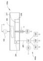
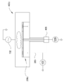
KR20180122295A - 수동 방식으로 동작되는 경우에 접지에 대한 제어가능한 임피던스를 가능하게 하고 능동적으로 전력공급되는 경우에 플라즈마로의 대칭적인 rf 전력 입력을 가능하게 하는 대칭적인 피드 구조 및 드라이브를 갖는 보조 전극을 사용하여 플라즈마 프로세싱 챔버에서 웨이퍼 에지 시스를 조절하기 위한 방법 - Google Patents
수동 방식으로 동작되는 경우에 접지에 대한 제어가능한 임피던스를 가능하게 하고 능동적으로 전력공급되는 경우에 플라즈마로의 대칭적인 rf 전력 입력을 가능하게 하는 대칭적인 피드 구조 및 드라이브를 갖는 보조 전극을 사용하여 플라즈마 프로세싱 챔버에서 웨이퍼 에지 시스를 조절하기 위한 방법 Download PDFInfo
- Publication number
- KR20180122295A KR20180122295A KR1020180050689A KR20180050689A KR20180122295A KR 20180122295 A KR20180122295 A KR 20180122295A KR 1020180050689 A KR1020180050689 A KR 1020180050689A KR 20180050689 A KR20180050689 A KR 20180050689A KR 20180122295 A KR20180122295 A KR 20180122295A
- Authority
- KR
- South Korea
- Prior art keywords
- processing chamber
- electrode
- disposed
- assembly
- semicircular
- Prior art date
- Legal status (The legal status is an assumption and is not a legal conclusion. Google has not performed a legal analysis and makes no representation as to the accuracy of the status listed.)
- Ceased
Links
Images


Classifications
-
- H—ELECTRICITY
- H01—ELECTRIC ELEMENTS
- H01J—ELECTRIC DISCHARGE TUBES OR DISCHARGE LAMPS
- H01J37/00—Discharge tubes with provision for introducing objects or material to be exposed to the discharge, e.g. for the purpose of examination or processing thereof
- H01J37/32—Gas-filled discharge tubes
- H01J37/32431—Constructional details of the reactor
- H01J37/32623—Mechanical discharge control means
- H01J37/32642—Focus rings
-
- H—ELECTRICITY
- H01—ELECTRIC ELEMENTS
- H01J—ELECTRIC DISCHARGE TUBES OR DISCHARGE LAMPS
- H01J37/00—Discharge tubes with provision for introducing objects or material to be exposed to the discharge, e.g. for the purpose of examination or processing thereof
- H01J37/32—Gas-filled discharge tubes
- H01J37/32431—Constructional details of the reactor
-
- H—ELECTRICITY
- H01—ELECTRIC ELEMENTS
- H01J—ELECTRIC DISCHARGE TUBES OR DISCHARGE LAMPS
- H01J37/00—Discharge tubes with provision for introducing objects or material to be exposed to the discharge, e.g. for the purpose of examination or processing thereof
- H01J37/32—Gas-filled discharge tubes
- H01J37/32009—Arrangements for generation of plasma specially adapted for examination or treatment of objects, e.g. plasma sources
- H01J37/32082—Radio frequency generated discharge
- H01J37/32174—Circuits specially adapted for controlling the RF discharge
- H01J37/32183—Matching circuits
-
- H—ELECTRICITY
- H01—ELECTRIC ELEMENTS
- H01J—ELECTRIC DISCHARGE TUBES OR DISCHARGE LAMPS
- H01J37/00—Discharge tubes with provision for introducing objects or material to be exposed to the discharge, e.g. for the purpose of examination or processing thereof
- H01J37/32—Gas-filled discharge tubes
- H01J37/32431—Constructional details of the reactor
- H01J37/32532—Electrodes
-
- H—ELECTRICITY
- H10—SEMICONDUCTOR DEVICES; ELECTRIC SOLID-STATE DEVICES NOT OTHERWISE PROVIDED FOR
- H10P—GENERIC PROCESSES OR APPARATUS FOR THE MANUFACTURE OR TREATMENT OF DEVICES COVERED BY CLASS H10
- H10P72/00—Handling or holding of wafers, substrates or devices during manufacture or treatment thereof
- H10P72/04—Apparatus for manufacture or treatment
- H10P72/0402—Apparatus for fluid treatment
- H10P72/0418—Apparatus for fluid treatment for etching
- H10P72/0421—Apparatus for fluid treatment for etching for drying etching
-
- H—ELECTRICITY
- H10—SEMICONDUCTOR DEVICES; ELECTRIC SOLID-STATE DEVICES NOT OTHERWISE PROVIDED FOR
- H10P—GENERIC PROCESSES OR APPARATUS FOR THE MANUFACTURE OR TREATMENT OF DEVICES COVERED BY CLASS H10
- H10P72/00—Handling or holding of wafers, substrates or devices during manufacture or treatment thereof
- H10P72/70—Handling or holding of wafers, substrates or devices during manufacture or treatment thereof for supporting or gripping
- H10P72/72—Handling or holding of wafers, substrates or devices during manufacture or treatment thereof for supporting or gripping using electrostatic chucks
- H10P72/722—Details of electrostatic chucks
-
- H—ELECTRICITY
- H01—ELECTRIC ELEMENTS
- H01J—ELECTRIC DISCHARGE TUBES OR DISCHARGE LAMPS
- H01J2237/00—Discharge tubes exposing object to beam, e.g. for analysis treatment, etching, imaging
- H01J2237/32—Processing objects by plasma generation
- H01J2237/33—Processing objects by plasma generation characterised by the type of processing
- H01J2237/334—Etching
-
- H—ELECTRICITY
- H01—ELECTRIC ELEMENTS
- H01J—ELECTRIC DISCHARGE TUBES OR DISCHARGE LAMPS
- H01J37/00—Discharge tubes with provision for introducing objects or material to be exposed to the discharge, e.g. for the purpose of examination or processing thereof
- H01J37/32—Gas-filled discharge tubes
- H01J37/32431—Constructional details of the reactor
- H01J37/32715—Workpiece holder
-
- H—ELECTRICITY
- H10—SEMICONDUCTOR DEVICES; ELECTRIC SOLID-STATE DEVICES NOT OTHERWISE PROVIDED FOR
- H10P—GENERIC PROCESSES OR APPARATUS FOR THE MANUFACTURE OR TREATMENT OF DEVICES COVERED BY CLASS H10
- H10P72/00—Handling or holding of wafers, substrates or devices during manufacture or treatment thereof
- H10P72/04—Apparatus for manufacture or treatment
- H10P72/0431—Apparatus for thermal treatment
- H10P72/0432—Apparatus for thermal treatment mainly by conduction
-
- H—ELECTRICITY
- H10—SEMICONDUCTOR DEVICES; ELECTRIC SOLID-STATE DEVICES NOT OTHERWISE PROVIDED FOR
- H10P—GENERIC PROCESSES OR APPARATUS FOR THE MANUFACTURE OR TREATMENT OF DEVICES COVERED BY CLASS H10
- H10P72/00—Handling or holding of wafers, substrates or devices during manufacture or treatment thereof
- H10P72/70—Handling or holding of wafers, substrates or devices during manufacture or treatment thereof for supporting or gripping
- H10P72/76—Handling or holding of wafers, substrates or devices during manufacture or treatment thereof for supporting or gripping using mechanical means, e.g. clamps or pinches
- H10P72/7604—Handling or holding of wafers, substrates or devices during manufacture or treatment thereof for supporting or gripping using mechanical means, e.g. clamps or pinches the wafers being placed on a susceptor, stage or support
- H10P72/7612—Handling or holding of wafers, substrates or devices during manufacture or treatment thereof for supporting or gripping using mechanical means, e.g. clamps or pinches the wafers being placed on a susceptor, stage or support characterised by lifting arrangements, e.g. lift pins
Landscapes
- Physics & Mathematics (AREA)
- Engineering & Computer Science (AREA)
- Plasma & Fusion (AREA)
- Chemical & Material Sciences (AREA)
- Analytical Chemistry (AREA)
- Drying Of Semiconductors (AREA)
- Plasma Technology (AREA)
- Container, Conveyance, Adherence, Positioning, Of Wafer (AREA)
Applications Claiming Priority (2)
| Application Number | Priority Date | Filing Date | Title |
|---|---|---|---|
| US201762500120P | 2017-05-02 | 2017-05-02 | |
| US62/500,120 | 2017-05-02 |
Publications (1)
| Publication Number | Publication Date |
|---|---|
| KR20180122295A true KR20180122295A (ko) | 2018-11-12 |
Family
ID=64015476
Family Applications (1)
| Application Number | Title | Priority Date | Filing Date |
|---|---|---|---|
| KR1020180050689A Ceased KR20180122295A (ko) | 2017-05-02 | 2018-05-02 | 수동 방식으로 동작되는 경우에 접지에 대한 제어가능한 임피던스를 가능하게 하고 능동적으로 전력공급되는 경우에 플라즈마로의 대칭적인 rf 전력 입력을 가능하게 하는 대칭적인 피드 구조 및 드라이브를 갖는 보조 전극을 사용하여 플라즈마 프로세싱 챔버에서 웨이퍼 에지 시스를 조절하기 위한 방법 |
Country Status (5)
| Country | Link |
|---|---|
| US (1) | US20180323042A1 (enExample) |
| JP (1) | JP2018190978A (enExample) |
| KR (1) | KR20180122295A (enExample) |
| CN (2) | CN209266350U (enExample) |
| TW (1) | TW201907439A (enExample) |
Families Citing this family (23)
| Publication number | Priority date | Publication date | Assignee | Title |
|---|---|---|---|---|
| US9873180B2 (en) | 2014-10-17 | 2018-01-23 | Applied Materials, Inc. | CMP pad construction with composite material properties using additive manufacturing processes |
| US11745302B2 (en) | 2014-10-17 | 2023-09-05 | Applied Materials, Inc. | Methods and precursor formulations for forming advanced polishing pads by use of an additive manufacturing process |
| US10875153B2 (en) | 2014-10-17 | 2020-12-29 | Applied Materials, Inc. | Advanced polishing pad materials and formulations |
| WO2016060712A1 (en) | 2014-10-17 | 2016-04-21 | Applied Materials, Inc. | Cmp pad construction with composite material properties using additive manufacturing processes |
| US9776361B2 (en) | 2014-10-17 | 2017-10-03 | Applied Materials, Inc. | Polishing articles and integrated system and methods for manufacturing chemical mechanical polishing articles |
| US10593574B2 (en) | 2015-11-06 | 2020-03-17 | Applied Materials, Inc. | Techniques for combining CMP process tracking data with 3D printed CMP consumables |
| US10391605B2 (en) | 2016-01-19 | 2019-08-27 | Applied Materials, Inc. | Method and apparatus for forming porous advanced polishing pads using an additive manufacturing process |
| US11471999B2 (en) | 2017-07-26 | 2022-10-18 | Applied Materials, Inc. | Integrated abrasive polishing pads and manufacturing methods |
| CN112654655A (zh) | 2018-09-04 | 2021-04-13 | 应用材料公司 | 先进抛光垫配方 |
| JP6960390B2 (ja) * | 2018-12-14 | 2021-11-05 | 東京エレクトロン株式会社 | 給電構造及びプラズマ処理装置 |
| WO2020146034A1 (en) * | 2019-01-08 | 2020-07-16 | Applied Materials, Inc. | Recursive coils for inductively coupled plasmas |
| CN114743854B (zh) | 2019-05-14 | 2025-02-25 | 玛特森技术公司 | 末端执行器和用于处理工件的系统 |
| KR102848754B1 (ko) * | 2019-07-29 | 2025-08-20 | 어플라이드 머티어리얼스, 인코포레이티드 | 개선된 고온 척킹을 갖는 반도체 기판 지지부들 |
| JP2021103641A (ja) * | 2019-12-25 | 2021-07-15 | 東京エレクトロン株式会社 | プラズマ発生源の検査方法及び負荷 |
| JP7454961B2 (ja) * | 2020-03-05 | 2024-03-25 | 東京エレクトロン株式会社 | プラズマ処理装置 |
| JP7344821B2 (ja) * | 2020-03-17 | 2023-09-14 | 東京エレクトロン株式会社 | プラズマ処理装置 |
| CN112331607B (zh) * | 2020-10-28 | 2024-03-26 | 北京北方华创微电子装备有限公司 | 静电卡盘及半导体工艺设备 |
| JP7544450B2 (ja) * | 2021-03-17 | 2024-09-03 | 東京エレクトロン株式会社 | プラズマ処理装置 |
| JP7557429B2 (ja) * | 2021-05-27 | 2024-09-27 | 東京エレクトロン株式会社 | プラズマ処理装置 |
| KR102932754B1 (ko) * | 2021-12-24 | 2026-03-04 | 삼성전자주식회사 | 에지 링 어셈블리를 포함하는 기판 처리 장치 및 이를 이용한 기판 처리 방법 |
| WO2025164456A1 (ja) * | 2024-02-02 | 2025-08-07 | 東京エレクトロン株式会社 | プラズマ処理装置 |
| US12463075B2 (en) * | 2024-02-23 | 2025-11-04 | Applied Materials, Inc. | Cathode assembly for integration of embedded electrostatic chuck (ESC) |
| US20250299929A1 (en) * | 2024-03-25 | 2025-09-25 | Applied Materials, Inc. | Substrate support assembly having an edge voltage delivery system |
Family Cites Families (11)
| Publication number | Priority date | Publication date | Assignee | Title |
|---|---|---|---|---|
| US5822171A (en) * | 1994-02-22 | 1998-10-13 | Applied Materials, Inc. | Electrostatic chuck with improved erosion resistance |
| US5633073A (en) * | 1995-07-14 | 1997-05-27 | Applied Materials, Inc. | Ceramic susceptor with embedded metal electrode and eutectic connection |
| KR100796830B1 (ko) * | 2000-04-12 | 2008-01-22 | 아익스트론 아게 | 기판코팅방법 수행용 반응실 |
| US7311784B2 (en) * | 2002-11-26 | 2007-12-25 | Tokyo Electron Limited | Plasma processing device |
| US7572737B1 (en) * | 2006-06-30 | 2009-08-11 | Lam Research Corporation | Apparatus and methods for adjusting an edge ring potential substrate processing |
| US9536711B2 (en) * | 2007-03-30 | 2017-01-03 | Lam Research Corporation | Method and apparatus for DC voltage control on RF-powered electrode |
| US8691047B2 (en) * | 2009-11-17 | 2014-04-08 | Applied Materials, Inc. | Large area plasma processing chamber with at-electrode RF matching |
| US9443753B2 (en) * | 2010-07-30 | 2016-09-13 | Applied Materials, Inc. | Apparatus for controlling the flow of a gas in a process chamber |
| KR101202957B1 (ko) * | 2010-10-19 | 2012-11-20 | 주성엔지니어링(주) | 플라즈마 발생용 안테나 및 이를 포함하는 기판처리장치 |
| US9412579B2 (en) * | 2012-04-26 | 2016-08-09 | Applied Materials, Inc. | Methods and apparatus for controlling substrate uniformity |
| US10580623B2 (en) * | 2013-11-19 | 2020-03-03 | Applied Materials, Inc. | Plasma processing using multiple radio frequency power feeds for improved uniformity |
-
2018
- 2018-04-19 US US15/957,054 patent/US20180323042A1/en not_active Abandoned
- 2018-04-29 JP JP2018087886A patent/JP2018190978A/ja active Pending
- 2018-05-02 CN CN201820642742.8U patent/CN209266350U/zh not_active Expired - Fee Related
- 2018-05-02 TW TW107114804A patent/TW201907439A/zh unknown
- 2018-05-02 CN CN201810410921.3A patent/CN108807125A/zh active Pending
- 2018-05-02 KR KR1020180050689A patent/KR20180122295A/ko not_active Ceased
Also Published As
| Publication number | Publication date |
|---|---|
| CN108807125A (zh) | 2018-11-13 |
| TW201907439A (zh) | 2019-02-16 |
| US20180323042A1 (en) | 2018-11-08 |
| JP2018190978A (ja) | 2018-11-29 |
| CN209266350U (zh) | 2019-08-16 |
Similar Documents
| Publication | Publication Date | Title |
|---|---|---|
| US20180323042A1 (en) | Method to modulate the wafer edge sheath in a plasma processing chamber | |
| US11908666B2 (en) | Stage and plasma processing apparatus | |
| KR102749806B1 (ko) | 에지-국부화된 이온 궤적 제어 및 플라즈마 동작을 통한 선단 에지 시스 및 웨이퍼 프로파일 튜닝 | |
| US10615004B2 (en) | Distributed electrode array for plasma processing | |
| US10770328B2 (en) | Substrate support with symmetrical feed structure | |
| US12198906B2 (en) | Substrate support and plasma processing apparatus | |
| JP5564549B2 (ja) | 可変静電容量を有するプラズマ処理システムのための方法および装置 | |
| US6262538B1 (en) | High density plasma tool with adjustable uniformity and stochastic electron heating for reduced gas cracking | |
| CN110858531A (zh) | 用于在等离子体处理腔室中的基板支撑件的边缘环组件 | |
| KR102786117B1 (ko) | 급전 구조 및 플라즈마 처리 장치 | |
| KR20180122964A (ko) | 액티브 파 에지 플라즈마 튜닝가능성 | |
| WO2022201351A1 (ja) | プラズマ処理装置およびプラズマ処理方法 | |
| US20250379090A1 (en) | Electrostatic chucks with hybrid pucks to improve thermal performance and leakage current stability |
Legal Events
| Date | Code | Title | Description |
|---|---|---|---|
| PA0109 | Patent application |
Patent event code: PA01091R01D Comment text: Patent Application Patent event date: 20180502 |
|
| PG1501 | Laying open of application | ||
| PA0201 | Request for examination |
Patent event code: PA02012R01D Patent event date: 20210430 Comment text: Request for Examination of Application Patent event code: PA02011R01I Patent event date: 20180502 Comment text: Patent Application |
|
| E902 | Notification of reason for refusal | ||
| PE0902 | Notice of grounds for rejection |
Comment text: Notification of reason for refusal Patent event date: 20221014 Patent event code: PE09021S01D |
|
| E601 | Decision to refuse application | ||
| PE0601 | Decision on rejection of patent |
Patent event date: 20221219 Comment text: Decision to Refuse Application Patent event code: PE06012S01D Patent event date: 20221014 Comment text: Notification of reason for refusal Patent event code: PE06011S01I |