KR20180098429A - Embedded type temperature measuring wafer sensor and method for fabricating the same - Google Patents
Embedded type temperature measuring wafer sensor and method for fabricating the same Download PDFInfo
- Publication number
- KR20180098429A KR20180098429A KR1020170024524A KR20170024524A KR20180098429A KR 20180098429 A KR20180098429 A KR 20180098429A KR 1020170024524 A KR1020170024524 A KR 1020170024524A KR 20170024524 A KR20170024524 A KR 20170024524A KR 20180098429 A KR20180098429 A KR 20180098429A
- Authority
- KR
- South Korea
- Prior art keywords
- wafer
- temperature measuring
- measuring unit
- temperature
- sensor
- Prior art date
- Legal status (The legal status is an assumption and is not a legal conclusion. Google has not performed a legal analysis and makes no representation as to the accuracy of the status listed.)
- Ceased
Links
Images


Classifications
-
- H—ELECTRICITY
- H10—SEMICONDUCTOR DEVICES; ELECTRIC SOLID-STATE DEVICES NOT OTHERWISE PROVIDED FOR
- H10P—GENERIC PROCESSES OR APPARATUS FOR THE MANUFACTURE OR TREATMENT OF DEVICES COVERED BY CLASS H10
- H10P74/00—Testing or measuring during manufacture or treatment of wafers, substrates or devices
- H10P74/20—Testing or measuring during manufacture or treatment of wafers, substrates or devices characterised by the properties tested or measured, e.g. structural or electrical properties
- H10P74/203—Structural properties, e.g. testing or measuring thicknesses, line widths, warpage, bond strengths or physical defects
-
- H01L22/12—
-
- H01L21/67248—
-
- H01L22/30—
-
- H01L35/32—
-
- H—ELECTRICITY
- H10—SEMICONDUCTOR DEVICES; ELECTRIC SOLID-STATE DEVICES NOT OTHERWISE PROVIDED FOR
- H10N—ELECTRIC SOLID-STATE DEVICES NOT OTHERWISE PROVIDED FOR
- H10N10/00—Thermoelectric devices comprising a junction of dissimilar materials, i.e. devices exhibiting Seebeck or Peltier effects
- H10N10/10—Thermoelectric devices comprising a junction of dissimilar materials, i.e. devices exhibiting Seebeck or Peltier effects operating with only the Peltier or Seebeck effects
- H10N10/17—Thermoelectric devices comprising a junction of dissimilar materials, i.e. devices exhibiting Seebeck or Peltier effects operating with only the Peltier or Seebeck effects characterised by the structure or configuration of the cell or thermocouple forming the device
-
- H—ELECTRICITY
- H10—SEMICONDUCTOR DEVICES; ELECTRIC SOLID-STATE DEVICES NOT OTHERWISE PROVIDED FOR
- H10P—GENERIC PROCESSES OR APPARATUS FOR THE MANUFACTURE OR TREATMENT OF DEVICES COVERED BY CLASS H10
- H10P72/00—Handling or holding of wafers, substrates or devices during manufacture or treatment thereof
- H10P72/06—Apparatus for monitoring, sorting, marking, testing or measuring
- H10P72/0602—Temperature monitoring
-
- H—ELECTRICITY
- H10—SEMICONDUCTOR DEVICES; ELECTRIC SOLID-STATE DEVICES NOT OTHERWISE PROVIDED FOR
- H10P—GENERIC PROCESSES OR APPARATUS FOR THE MANUFACTURE OR TREATMENT OF DEVICES COVERED BY CLASS H10
- H10P74/00—Testing or measuring during manufacture or treatment of wafers, substrates or devices
- H10P74/27—Structural arrangements therefor
Landscapes
- Engineering & Computer Science (AREA)
- Manufacturing & Machinery (AREA)
- Testing Or Measuring Of Semiconductors Or The Like (AREA)
Abstract
Description
본 발명은 온도측정 웨이퍼 센서 및 그 제조방법에 관한 것으로서, 특히 온도측정부의 열이 외부로 빠져나가는 것을 방지할 수 있고, 온도측정부로서의 특성을 안정되게 지속적으로 장기간 유지시킬 수 있는, 매립형 온도측정 웨이퍼 센서 및 그 제조방법에 관한 것이다. The present invention relates to a temperature measuring wafer sensor and a manufacturing method thereof, and more particularly, to a temperature measuring wafer sensor capable of preventing the heat of the temperature measuring unit from escaping to the outside, and capable of stably and continuously maintaining the characteristics of the temperature measuring unit for a long period. To a wafer sensor and a manufacturing method thereof.
온도센서용 웨이퍼는 웨이퍼가 들어 있는 반응장치 속에서 반응이 진행될 때, 웨이퍼의 실제온도가 얼마인지를 간접적으로 측정하기 위한 센서로, 웨이퍼 표면에 홈을 낸 후에 홈에 열전쌍(thermocouple)을 심어 놓은 것이다. 이 온도센서용 웨이퍼를 반응장치 속에 웨이퍼 대신 넣은 후, 반응장치를 실제 반응시와 동일한 조건으로 만들어 놓은 상태에서 온도센서용 웨이퍼에 심어져 있는 열전쌍으로부터 나오는 열기전력을 측정하여 온도로 환산하면, 실제 반응시의 웨이퍼의 온도를 간접적으로 측정할 수 있다. 열전쌍은 그 고유특성상 열전쌍접점이 위치한 곳의 온도에 비례하는 열기전력을 발생하는 것이며, 그 열기전력을 증폭시켜 온도로서 환산시켜 온도측정을 하는 측정기의 센서로서 사용된다.A wafer for a temperature sensor is a sensor for indirectly measuring the actual temperature of the wafer when the reaction proceeds in a reactor containing the wafer. The wafer is thermocouple-plated will be. When the temperature sensor wafer is placed in the reactor in place of the wafer and the reaction apparatus is made in the same condition as the actual reaction, the thermoelectric power generated from the thermocouple embedded in the wafer for the temperature sensor is measured and converted into a temperature The temperature of the wafer at the time of the reaction can be indirectly measured. The thermocouple generates thermoelectric power proportional to the temperature at the thermocouple contact point in its inherent characteristics and is used as a sensor of a measuring device for measuring the temperature by converting the thermoelectric power into a temperature by amplifying the thermoelectric power.
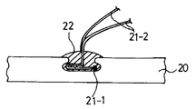
도 1은 종래의 제 1 기술에 의한 온도센서용 웨이퍼를 나타낸 단면도이다. 웨이퍼(10)에 홈을 파서 열전쌍(11)의 열전쌍접점(11-1)을 세라믹류의 본딩물질(12)로 밀봉하고, 열전쌍접점(11-1)에 연결된 열전쌍연결선(11-2)의 대부분을 웨이퍼(10)의 외부에 노출시킨 구조를 가지고 있다.1 is a cross-sectional view showing a wafer for a temperature sensor according to a first conventional technique. A groove is formed in the
웨이퍼가 반응장치내에서 복사광을 받아 온도가 상승할 경우에 웨이퍼 주변의 분위기 온도는 웨이퍼의 온도보다 낮은 상태가 되는데, 종래의 온도센서용 웨이퍼는 열전쌍연결선의 웨이퍼 속에 파묻힌 부분의 길이가 짧기 때문에 온도에 따른 기전력을 발생시키는 열전쌍접점의 열이 열전도가 좋은 열전쌍연결선을 통하여 쉽게 웨이퍼 외부로 빠져나가게 된다. 그에 따라 그 접점의 온도는 웨이퍼의 실제 온도보다 낮게 나타나게 된다. 예를 들어, 웨이퍼 주변의 분위기 온도가 1000℃정도일 경우에 측정되는 온도는 약 15∼20℃정도 낮게 나타난다. 즉, 상기와 같은 종래의 온도센서용 웨이퍼는 온도응답속도가 느리고, 웨이퍼의 주변온도에 영향을 많이 받는 단점이 있다.The ambient temperature around the wafer is lower than the temperature of the wafer when the temperature of the wafer is increased due to the radiation of the radiation in the reaction apparatus because the length of the portion of the thermocouple connecting wire embedded in the wafer is short The heat of the thermocouple contact, which generates the electromotive force according to the temperature, easily escapes to the outside of the wafer through the thermocouple connecting line with good thermal conductivity. So that the temperature of the contact point is lower than the actual temperature of the wafer. For example, when the ambient temperature around the wafer is about 1000 ° C, the measured temperature is about 15 to 20 ° C lower. That is, the conventional wafer for a temperature sensor as described above has a disadvantage in that the temperature response speed is slow and is greatly influenced by the ambient temperature of the wafer.
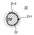
도 2a와 도 2b는 종래의 제 2 기술에 의한 온도센서용 웨이퍼의 단면도와 평면도를 각각 나타낸 것이다. 평면도(도 2b)에 보인 열전쌍연결선은 본딩물질에 파묻힌 부분만을 나타낸 것이다. 열전쌍접점(21-1)만 웨이퍼(20)속에 묻힌 것이 아니라, 웨이퍼(20)에 형성된 홀에 열전쌍연결선(21-2)을 반원형으로 휘어 넣어서 세라믹류의 본딩물질(23)로 밀봉한 것이다. 이 때, 열전쌍접점(21-1)에 연결된 열전쌍연결선(21-2)은 그 일부가 노출되어 있다. 도 2b에서 20은 웨이퍼를 나타낸 것이다.2A and 2B are respectively a cross-sectional view and a plan view of a wafer for a temperature sensor according to a second conventional technique. The thermocouple connecting line shown in the plan view (FIG. 2B) shows only the portion embedded in the bonding material. Not only the thermocouple contact 21-1 is embedded in the
일반적으로 물질의 단위시간당 흘러나가는 열량은 열전도도, 열전쌍연결선의 단면적 및 온도차에 비례하고 열전쌍연결선의 길이에 반비례한다. 이를 상기 종래 기술에 적용하면, 웨이퍼 내부의 온도와 웨이퍼 외부의 온도가 같고, 열전쌍연결선의 단면적과 열전도도가 같은 경우에는 열전쌍연결선을 통하여 흘러나가는 열량은 열전쌍연결선의 길이에 반비례한다. 따라서, 종래 제 2 기술에 보인 온도센서용 웨이퍼와 같이, 열전쌍연결선을 반원형으로 풀어 사용할 경우, 웨이퍼 속에 파묻힌 열전쌍연결선의 길이가 길어서 상대적으로 열전쌍접점의 열이 빠져나오지는 않기 때문에 보다 정확한 웨이퍼의 온도측정을 할 수 있다.In general, the amount of heat flowing per unit time of a material is proportional to the thermal conductivity, the cross-sectional area of the thermocouple connection line, and the temperature difference, and is inversely proportional to the length of the thermocouple connection line. When the temperature inside the wafer is equal to the temperature outside the wafer and the cross-sectional area and the thermal conductivity of the thermocouple connection line are the same, the amount of heat flowing through the thermocouple connection line is inversely proportional to the length of the thermocouple connection line. Therefore, when the thermocouple connecting line is unloaded in a semicircular shape as in the case of the temperature sensor wafer according to the second technique, since the length of the thermocouple connecting line embedded in the wafer is long and the heat of the thermocouple contact is not released relatively, Measurement can be performed.
그러나 종래의 제 2 기술에 의한 온도센서용 웨이퍼는 제작하는 과정에서 열전쌍연결선을 웨이퍼의 홈에 휘어넣기가 어렵고, 상기 온도센서용 웨이퍼를 사용하는 중에는 열전쌍연결선의 휘어진 부분이 쉽게 열화되기 때문에 수명이 짧아지는 단점이 있다.However, it is difficult to bend the thermocouple connecting line into the groove of the wafer in the manufacturing process of the temperature sensor wafer according to the second conventional technique, and the bent part of the thermocouple connecting line is easily deteriorated during the use of the temperature sensor wafer, There is a shortcoming.
또한, 일부에서는 상기한 본딩물질(22, 23) 대신에 필름을 이용해서 열전쌍접점(11-1, 21-1)과 열전쌍연결선(21-1, 21-2)을 연결하기도 한다. 그러나, 이와 같이 필름을 이용하는 것은 제조하기는 쉽지만, 필름 자체의 특성 때문에 고온에서 불안정하고, 열전쌍연결선이 쉽게 끓어지거나 얇게 연결되는 등의 단점이 있다. In some cases, the thermocouple contacts 11-1 and 21-1 and the thermocouple connecting lines 21-1 and 21-2 are connected to each other by using a film instead of the
따라서 본 발명이 해결하고자 하는 과제는, 온도측정부의 열이 외부로 빠져나가는 것을 방지할 수 있을 뿐만 아니라, 온도측정부로서의 특성을 안정되게 지속적으로 장기간 유지시킬 수 있는, 매립형 온도측정 웨이퍼 센서 및 그 제조방법을 제공하는 것이다. SUMMARY OF THE INVENTION Accordingly, it is an object of the present invention to provide a buried temperature measurement wafer sensor which can prevent the heat of the temperature measurement unit from escaping to the outside, and can stably and continuously maintain the characteristics of the temperature measurement unit for a long period, And a method for manufacturing the same.
본 발명의 일 실시형태에 따른 매립형 온도측정 웨이퍼 센서는, 웨이퍼 상에 온도측정부가 구비된 웨이퍼 센서에 있어서, 상기 웨이퍼는 상기 온도측정부가 매립되는 매립홈을 가지고, 상기 온도측정부는 상기 매립홈에 매립된 것을 특징으로 한다. A buried temperature measurement wafer sensor according to an embodiment of the present invention is a wafer sensor having a temperature measurement unit on a wafer, wherein the wafer has a buried groove in which the temperature measurement unit is buried, And is embedded.
상기 온도측정부는 온도센서와 상기 온도센서를 웨이퍼 외부와 연결하는 연결배선을 포함하고, 상기 온도센서와 연결배선은 상기 매립홈에 매립된 것이 가능하다. The temperature measuring unit may include a temperature sensor and a connection wiring for connecting the temperature sensor to the outside of the wafer, and the temperature sensor and the connection wiring may be embedded in the buried groove.
상기 온도측정부는 열전쌍(thermocouple)인 것일 수 있다. The temperature measuring unit may be a thermocouple.
상기 온도측정부는 서로 다른 물질로 이루어진 제1연결배선과 제2연결배선; 및 상기 제1연결배선과 제2연결배선이 접점된 접점부;를 가지고, 상기 제1연결배선과 제2연결배선; 및 접점부;는 상기 매립홈에 매립된 것이 바람직하다. The temperature measuring unit may include a first connection wiring and a second connection wiring made of different materials; And a contact portion to which the first connection wiring and the second connection wiring are contacted, wherein the first connection wiring and the second connection wiring; And the contact portion are embedded in the buried groove.
상기 매립홈은 웨이퍼의 최외각 끝까지 형성된 것이 가능하다. The buried groove can be formed to the outermost end of the wafer.
상기 매립홈은 내부에 절연층을 가지고, 상기 절연층 위에 온도측정부가 매립된 것일 수 있다. The buried groove may have an insulating layer inside, and the temperature measuring part may be embedded on the insulating layer.
상기 웨이퍼는 상기 온도측정부를 덮는 보호층을 더 포함하는 것이 바람직하다.The wafer may further include a protective layer covering the temperature measuring unit.
상기 온도측정부는 금속물질이 상기 매립홈에 증착된 것이 가능하다. The temperature measuring part can deposit a metal material in the buried groove.
상기 온도측정부는 와이어가 상기 매립홈에 삽입된 것일 수 있다. The temperature measuring part may be a wire inserted into the buried groove.
상기 온도측정부는 금속물질로 이루어지고, 상기 금속물질은 구리, 금, 백금, 니켈, 티타늄 및 이것의 조합으로 이루어진 군에서 선택된 것이 바람직하다. Preferably, the temperature measuring unit is made of a metal material, and the metal material is selected from the group consisting of copper, gold, platinum, nickel, titanium, and combinations thereof.
상기 온도측정부는 2개 이상인 것이 가능하다. It is possible that there are two or more temperature measuring units.
본 발명의 다른 실시형태는, 상기한 웨이퍼 센서와, 상기 웨이퍼 센서가 올려지는 플레이트를 포함하는 웨이퍼 온도측정 시스템이다.Another embodiment of the present invention is a wafer temperature measurement system including the wafer sensor described above and a plate on which the wafer sensor is mounted.
본 발명의 또 다른 실시형태는, 웨이퍼 상에 온도측정부가 구비된 웨이퍼 센서의 제조방법에 있어서, 상기 웨이퍼 상에 온도측정부를 매립하기 위한 매립홈을 형성하는 단계; 상기 형성된 매립홈에 상기 온도측정부를 매립하는 단계; 및 상기 온도측정부를 덮는 보호층을 형성하는 단계;를 포함하는 것을 특징으로 하는 매립형 온도측정 웨이퍼 센서의 제조방법이다.According to still another aspect of the present invention, there is provided a method of manufacturing a wafer sensor having a temperature measurement unit on a wafer, the method comprising: forming a buried groove for filling a temperature measurement unit on the wafer; Burying the temperature measurement part in the formed buried groove; And forming a protective layer covering the temperature measurement unit. [7] The method according to claim 1,
본 발명에 의하면, 웨이퍼 상에 온도측정부가 매립되는 매립홈이 형성되어 있고 온도측정부는 상기 매립홈에 매립되어 있어서, 온도측정부를 충분히 두껍게 형성할 수 있기 때문에 상기 온도측정부가 벌크 성질을 갖도록 제조할 수 있고, 이를 통해서 고온에서도 안정한 효과를 갖는다. According to the present invention, since the buried groove for embedding the temperature measuring unit is formed on the wafer and the temperature measuring unit is embedded in the buried groove, the temperature measuring unit can be formed sufficiently thick so that the temperature measuring unit is manufactured to have a bulk property And it has a stable effect even at a high temperature.
또한, 본 발명은 온도측정부를 매립홈에 매립하여 제조함으로서, 상기 온도측정부의 열이 외부로 빠져나가는 것을 방지할 수 있을 뿐만 아니라, 끊어지지도 않고 안정하며, 온도측정부로서의 특성을 안정되게 지속적으로 장기간 유지시킬 수 있다. In addition, the present invention can prevent the heat of the temperature measuring unit from escaping to the outside by embedding the temperature measuring unit in the buried groove, and is also stable without being broken, and the characteristics of the temperature measuring unit can be stably and continuously It can be maintained for a long time.
나아가, 본 발명은 온도측정부를 매립홈에 매립하여 제조하기 때문에, 웨이퍼 위쪽 공간에 연결배선들이 없어서, 간결하고 단순한 형태의 온도측정 웨이퍼 센서를 제공할 수 있다. Further, since the present invention is manufactured by embedding the temperature measuring portion in the buried groove, there is no connecting wiring in the upper space of the wafer, so that it is possible to provide a simple and simple form of temperature measuring wafer sensor.
도 1은 종래 제 1 기술에 의한 온도센서용 웨이퍼의 단면도이고,
도 2a와 도 2b는 종래 제 2 기술에 의한 온도센서용 웨이퍼의 단면도와 평면도이고,
도 3은 본 발명의 일 실시예에 따른 매립형 온도측정 웨이퍼 센서(1)를 설명하기 위한 모식도이고,
도 4는 도 3의 단면도이고,
도 5는 본 발명에 따른 온도측정부가 열전쌍(thermocouple)인 것의 일례를 설명하기 위한 부분확대도이고,
도 6은 본 발명에 따른 매립홈에 절연층과 보호층이 형성된 것의 일례를 설명하기 위한 단면도이고,
도 7은 본 발명에 따른 매립홈이 웨이퍼의 최외각까지 형성된 것의 일례를 설명하기 위한 사시도이고,
도 8은 본 발명의 다른 일 실시예에 따른 매립형 온도측정 웨이퍼 센서의 제조방법을 설명하기 위한 순서도이다.
1 is a cross-sectional view of a wafer for a temperature sensor according to the first conventional technique,
2A and 2B are a cross-sectional view and a plan view of a wafer for a temperature sensor according to the second conventional technique,
3 is a schematic diagram for explaining a buried temperature measurement wafer sensor 1 according to an embodiment of the present invention,
4 is a cross-sectional view of Fig. 3,
5 is a partially enlarged view for explaining an example of a temperature measuring part according to the present invention being a thermocouple,
6 is a cross-sectional view for explaining an example in which an insulating layer and a protective layer are formed in buried grooves according to the present invention,
7 is a perspective view for explaining an example of a buried groove according to the present invention formed up to an outermost edge of a wafer,
8 is a flowchart illustrating a method of manufacturing a buried temperature measurement wafer sensor according to another embodiment of the present invention.
본 발명은 다양한 변환을 가할 수 있고 여러 가지 실시 예를 가질 수 있는 바, 특정 실시 예들을 도면에 예시하고 상세한 설명에서 상세하게 설명하고자 한다. 그러나, 이는 본 발명을 특정한 실시 형태에 대해 한정하려는 것이 아니며, 본 발명의 사상 및 기술 범위에 포함되는 모든 변환, 균등물 내지 대체물을 포함하는 것으로 이해되어야 한다. 본 발명을 설명함에 있어서 관련된 공지 기술에 대한 구체적인 설명이 본 발명의 요지를 흐릴 수 있다고 판단되는 경우 그 상세한 설명을 생략한다.BRIEF DESCRIPTION OF THE DRAWINGS The present invention is capable of various modifications and various embodiments, and specific embodiments are illustrated in the drawings and will be described in detail in the detailed description. It is to be understood, however, that the invention is not to be limited to the specific embodiments, but includes all modifications, equivalents, and alternatives falling within the spirit and scope of the invention. DETAILED DESCRIPTION OF THE PREFERRED EMBODIMENTS Hereinafter, the present invention will be described in detail with reference to the accompanying drawings.
본 출원에서 사용한 용어는 단지 특정한 실시예를 설명하기 위해 사용된 것으로, 본 발명을 한정하려는 의도가 아니다. 단수의 표현은 문맥상 명백하게 다르게 뜻하지 않는 한, 복수의 표현을 포함한다. 본 출원에서, "포함하다" 또는 "가지다" 등의 용어는 명세서상에 기재된 특징, 숫자, 단계, 동작, 구성요소, 부품 또는 이들을 조합한 것이 존재함을 지정하려는 것이지, 하나 또는 그 이상의 다른 특징들이나 숫자, 단계, 동작, 구성요소, 부품 또는 이들을 조합한 것들의 존재 또는 부가 가능성을 미리 배제하지 않는 것으로 이해되어야 한다.The terminology used herein is for the purpose of describing particular embodiments only and is not intended to be limiting of the invention. The singular expressions include plural expressions unless the context clearly dictates otherwise. In the present application, the terms "comprises" or "having" and the like are used to specify that there is a feature, a number, a step, an operation, an element, a component or a combination thereof described in the specification, But do not preclude the presence or addition of one or more other features, integers, steps, operations, elements, components, or combinations thereof.
제1, 제2 등의 용어는 다양한 구성요소들을 설명하는데 사용될 수 있지만, 상기 구성요소들은 상기 용어들에 의해 한정되어서는 안 된다. 상기 용어들은 하나의 구성요소를 다른 구성요소로부터 구별하는 목적으로만 사용된다. The terms first, second, etc. may be used to describe various components, but the components should not be limited by the terms. The terms are used only for the purpose of distinguishing one component from another.
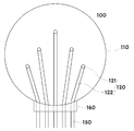
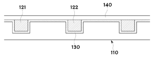
도 3은 본 발명의 일 실시예에 따른 매립형 온도측정 웨이퍼 센서(1)를 설명하기 위한 모식도이고, 도 4는 도 3의 단면도이다. FIG. 3 is a schematic view for explaining a buried temperature measurement wafer sensor 1 according to an embodiment of the present invention, and FIG. 4 is a sectional view of FIG.
여기에 도시된 바와 같이, 본 발명은 웨이퍼(110) 상에 온도측정부(120)가 구비된 웨이퍼 센서에 대한 것이다. As shown therein, the present invention is directed to a wafer sensor having a
상기 웨이퍼(110)는 반도체 제조용으로 사용되는 것일 수 있다. 그러나, 본 발명에서 웨이퍼(110)는 이것으로 제한되지 않는다. 상기 웨이퍼(110)는 전기로나 핫플레이트 등에 의해서 열처리되는 측정판, 또는 그와 같은 조건에서 사용되는 박판 등을 포함할 수 있다. 즉, 열처리 대상이 되는 박판이나, 그와 같은 표면 형상 및 그와 같은 열용량을 가지는 부재, 또는 열처리 대상이 되는 박판 그 자체일 수 있다. The
상기 온도측정부(120)는 웨이퍼(110) 상에서 상기 웨이퍼의 표면 온도를 측정할 수 있는 수단이다. 상기 온도측정부(120)는 열전쌍(thermocouple)이거나 저항체일 수 있다. 예를 들어, 열전변환소자(thermoelectric), 저항온도측정기(RTD; Resistance Temperature Detector), 측온 저항체(Thermoresistor)인 것이 가능하다. 본 발명자들은 온도측정부로서 열전쌍(thermocouple)을 기반으로 본 발명을 하였지만, 본 발명은 이외에 다양한 온도측정부에도 적용 가능하다. The
이러한 웨이퍼 센서(1)에 있어서, 본 발명에 의하면 상기 웨이퍼(110)는 상기 온도측정부(120)가 매립되는 매립홈(111)을 가지고, 상기 온도측정부(120)는 상기 매립홈(111)에 매립된 것을 특징으로 한다. 상기 매립홈(111)의 형상 내지 제조방법은 특별히 제한되지 않고, 이 기술분야에 알려진 모든 방법을 포함한다. 예를 들어, 상기 매립홈(111)은 식각 방법에 의해 사각형, 다각형, 또는 반원, 원형의 단면을 갖도록 형성될 수 있다. In the wafer sensor 1 according to the present invention, the
본 발명에 의하면, 웨이퍼(110) 상에 온도측정부(120)가 매립되는 매립홈(111)이 형성되어 있고 온도측정부(120)는 상기 매립홈(111)에 매립되어 있어서, 온도측정부(120)를 충분히 두껍게 형성할 수 있기 때문에 상기 온도측정부(120)가 벌크 성질을 갖도록 제조할 수 있고, 이를 통해서 고온에서도 안정한 효과를 갖는다. The
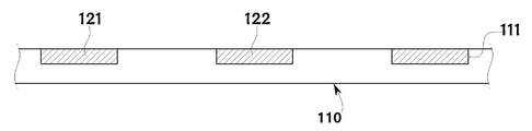
상기 온도측정부(120)는 1개 이상인 것이 가능하고, 2개 이상인 경우 웨이퍼 상(110)의 전체 온도를 균일하게 파악할 수 있어서 더욱 바람직하다. The number of the
또한, 상기 온도측정부(120)는 온도센서(121)와 상기 온도센서(121)를 웨이퍼(110) 외부와 연결하는 연결배선(122)을 포함하고, 상기 온도센서(121)와 연결배선(122)은 상기 매립홈(111)에 매립된 것이 가능하다. 상기 온도센서(121)는 웨이퍼(110) 상에서 실제로 온도를 측정하는 것이며, 상기 온도센서(121)는 상술한 온도측정부(120)와 동일한 것일 수 있다. 즉, 본 발명은 실제로 온도를 측정하는 온도센서(121) 뿐만 아니라 이와 연결된 연결배선(122) 까지도 매립홈(111)에 매립된 것이 바람직하다. 이러한 본 발명은 온도센서(121)와 연결배선(122)을 매립홈(111)에 매립하여 제조함으로서, 상기 연결배선(122)에 의해 열이 외부로 빠져나가는 것을 방지할 수 있을 뿐만 아니라, 끊어지지도 않고 안정하며, 온도측정부(120)로서의 특성을 안정되게 지속적으로 장기간 유지시킬 수 있다. The
또한, 상기 온도측정부(120) 또는 연결배선(122)은 금속물질이 상기 매립홈(111)에 증착된 것이 가능하다. 상기 금속물질은 특별히 제한되지 않고, 이 기술분야에 알려진 다양한 모든 것을 포함한다. 즉, 금속물질을 웨이퍼(110) 상의 매립홈(111)에 증착의 방법으로 형성하는 것이다. 그러면, 상기 온도측정부(120)를 매립홈(111)에 매립하기가 용이할 뿐만 아니라, 단단하게 고정시킬 수 있어서, 안정성이 높아지는 효과가 있다. In addition, the
다만, 본 발명은 상기 온도측정부(120) 또는 연결배선(122)이 금속물질로 이루어지고, 상기 금속물질은 구리, 금, 백금, 니켈, 티타늄 및 이것의 조합으로 이루어진 군에서 선택된 것이 바람직하다. 알루미늄은 가열하더라도 온도가 낮기 때문에, 구리, 금, 백금, 니켈, 티타늄 등을 사용하는 것이 바람직하다. 더욱 바람직하게는, 상기 금속물질로서 금(Au)이나 백금(Pt)을 이용할 수도 있지만, 웨이퍼(110) 상의 넓은 면적에 온도측정부(120) 또는 연결배선(122)을 형성하기 위해서는, 구리, 니켈, 티타늄 등을 이용하는 것이 제조의 편의성 측면에서 더욱 바람직하다. However, in the present invention, it is preferable that the
또한, 상기 온도측정부(120) 또는 연결배선(122)은 와이어가 상기 매립홈(111)에 삽입된 것일 수 있다. 즉, 본 발명에 따른 온도측정부(120) 또는 연결배선(122)을 증착이 아닌 와이어로 구성하는 것이다. 예를 들어, 금속 와이어를 매립홈(111)에 삽입하여 제조할 수 있다. 이와 같이 와이어를 이용하는 것은 웨이퍼(110) 상에 본 발명처럼 매립홈(111)이 이미 형성되어 있기 때문에, 구현 가능한 것이다. The
도 5는 본 발명에 따른 온도측정부(120)가 열전쌍(thermocouple)인 것의 일례를 설명하기 위한 부분확대도이고, 여기에 도시된 바와 같이, 본 발명에 따른 온도측정부(120)는 열전쌍(thermocouple)일 수 있다. 5 is a partially enlarged view for explaining an example of the
기존에 열전쌍을 이용하는 온도측정용 웨이퍼 센서의 경우 열전쌍연결선에 의해 열이 외부로 유출되는 단점이 있었고, 필름을 이용해서 열전쌍접점에 열전쌍연결선을 연결하는 경우 필름 자체의 특성 때문에 고온에서 불안정하고, 열전쌍연결선이 쉽게 끓어지거나 얇게 연결되는 등의 단점이 있었다. Conventionally, in the case of a wafer sensor for temperature measurement using a thermocouple, there is a disadvantage in that heat is leaked to the outside by a thermocouple connecting line. When a thermocouple connecting line is connected to a thermocouple contact using a film, There is a disadvantage that the connection line is easily boiled or thinly connected.
그러나, 본 발명에 의하면, 열전쌍을 웨이퍼 상의 매립홈에 매립하기 때문에, 상기와 같은 단점이 없다. However, according to the present invention, since the thermocouple is buried in the buried groove on the wafer, there is no disadvantage as described above.
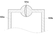
그 중에서도, 특히 상기 온도측정부(120)는 서로 다른 물질로 이루어진 제1연결배선(122a)과 제2연결배선(122b); 및 상기 제1연결배선(122a)과 제2연결배선(122b)이 접점된 접점부(121a);를 가지고, 상기 제1연결배선(122a)과 제2연결배선(122b); 및 접점부(121a);는 상기 매립홈(111)에 매립된 것이 바람직하다. 상기 서로 다른 물질은 상기한 금속물질 중 하나일 수 있다. 서로 다른 물질로 이루어진 제1연결배선(122a)과 제2연결배선(122b)을 이용하여, 그것의 일부가 중첩되도록 매립홈(111)에 매립함으로서, 온도측정부(120)를 열전쌍(thermocouple)으로 구현 가능하다. In particular, the
상기 접점부(121a)의 형상이나 크기는 특별히 제한되지 않는다. 즉, 상기 접점부(121a)는 원형, 사각형, 다각형, 일자형인 것이 가능하다.The shape and size of the
도 6은 본 발명에 따른 매립홈(111)에 절연층(120)과 보호층(140)이 형성된 것의 일례를 설명하기 위한 단면도이다.6 is a cross-sectional view illustrating an example in which an insulating
여기에 도시된 바와 같이, 본 발명의 다른 특징은 상기 매립홈(111)이 내부에 절연층(120)을 가지고, 상기 절연층(120) 위에 온도측정부(120)가 매립된 것일 수 있다. 매립홈(111)에 절연층(120)을 형성하는 방법은 특별히 제한되지 않고, 이 기술분야에 알려진 모든 형태를 포함한다. 이러한 본 발명은 온도측정부(120)와 웨이퍼(110) 사이에 절연층(120)을 포함함으로서, 상기 웨이퍼(110) 자체에 의한 온도편차의 영향을 방지하고, 매립홈(111)에 온도측정부(120)를 매설하는 것을 더욱 용이하게 할 수 있어서 바람직하다. As shown therein, another feature of the present invention is that the buried
또한, 본 발명에 의하면, 상기 웨이퍼(110)는 상기 온도측정부(120)를 덮는 보호층(140)을 더 포함하는 것이 바람직하다. 즉, 온도측정부(120) 위에 패시베이션 레이어를 덮는 것이다. 그러면, 웨이퍼(110) 위에서 들어오는 예기치 않은 외부변화나 또는 웨이퍼 상부의 상태 변화에 따른 영향을 방지할 수 있어서, 더욱 바람직하다. In addition, according to the present invention, the
도 7은 본 발명에 따른 매립홈(111)이 웨이퍼(110)의 최외각까지 형성된 것의 일례를 설명하기 위한 사시도이다. 7 is a perspective view for explaining an example of the embedding
여기에 도시된 바와 같이, 본 발명의 또 다른 특징은 상기 매립홈(111)이 웨이퍼(110)의 최외각 끝까지 형성된 것이다. As shown therein, another feature of the present invention is that the buried
기존에는 열전쌍연결선이 웨이퍼 상부로 드러나는 길이 또는 면적이 많았고, 일부에서는 열전쌍연결선의 선단부 뿐만 아니라 본체의 일부까지 매설하기도 하였지만, 여전히 열전쌍연결선의 일부는 외부로 드러나 있었다. In the past, thermocouple connection lines were exposed to the upper part of the wafer, and in some cases, not only the tip of the thermocouple connection line but also a part of the main body were buried, but still some of the thermocouple connection lines were exposed to the outside.
그러나, 본 발명은 웨이퍼(110) 상에 형성된 매립홈(111)을 통하여, 온도측정부(120) 전체를 웨이퍼(110)의 매립홈(111)에 매설한 것이 특징이고, 이를 통하여 고온에서도 안정하며, 온도센서로서의 특성을 안정되게 지속적으로 장기간 유지시킬 수 있다. However, the present invention is characterized in that the entire
이를 위하여, 본 발명은 웨이퍼(110)의 일부 측면에 온도측정부(120)의 연결배선(122)과 외부 리드배선(150)을 연결하는 연결단자(160)를 더 포함할 수도 있다(도 1 참조).To this end, the present invention may further include a
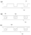
도 8은 본 발명의 다른 일 실시예에 따른 매립형 온도측정 웨이퍼 센서(1)의 제조방법을 설명하기 위한 순서도이다. 8 is a flowchart for explaining a method of manufacturing the buried temperature measurement wafer sensor 1 according to another embodiment of the present invention.
먼저, 도 8a에 도시된 바와 같이, 웨이퍼(110) 상에 온도측정부를 매립하기 위한 매립홈(111)을 형성하는 단계;를 거친다. 상기 매립홈(111)을 형성하는 방법은 특별히 제한되지 않는다. 상기 매립홈(111)의 형상이나 크기 역시 특별히 제한되지 않으며, 후술하는 온도측정부(120)를 매립할 수 있도록, 온도센서(121) 및/또는 연결배선(122)에 대응하는 것이 바람직하다. First, as shown in FIG. 8A, a step of forming a buried
다음에, 도 8b에서와 같이, 상기 형성된 매립홈(111)에 상기 온도측정부(120)를 매립하는 단계;를 거친다. 예를 들어, 금속물질을 증착하거나 와이어를 삽입해서 온도센서(121) 및/또는 연결배선(122)을 형성하는 것이 가능하다. 특히, 금속물질이나 와이어를 상기 매립홈(111)에만 매립하여 형성하는 것이 본 발명의 특징이다. 또한, 상기 온도센서(121) 및/또는 연결배선(122)의 상면은 웨이퍼(110)와 동일한 높이의 평면을 갖는 것이 바람직하다. Next, as shown in FIG. 8B, a step of embedding the
이어서, 도 8c에 도시된 바와 같이, 상기 온도측정부(120)를 덮는 보호층(140)을 형성하는 단계;를 거친다. 보호층(140)을 형성하는 방법은 특별히 제한되지 않고, 이 기술분야에 알려진 다양한 방법을 모두 이용할 수 있다. Next, as shown in FIG. 8C, forming a
한편, 본 발명은 상기한 웨이퍼 센서(1)와, 상기 웨이퍼 센서(1)가 올려지는 플레이트(도시하지 않음)를 포함하는 웨이퍼 온도측정 시스템이다. On the other hand, the present invention is a wafer temperature measurement system including the above-described wafer sensor 1 and a plate (not shown) on which the wafer sensor 1 is mounted.
상기 플레이트는 이 기술분야에 널리 알려진 다양한 형태를 포함한다. The plate includes various forms well known in the art.
이러한 웨이퍼 온도측정 시스템은 기존의 시스템에 적용되어 구현될 수 있고, 본 발명에 따른 웨이퍼 센서(1)를 위한 새로운 시스템으로 구현되는 것도 가능하다.Such a wafer temperature measurement system can be applied to an existing system and can be implemented as a new system for the wafer sensor 1 according to the present invention.
상기에서는 본 발명을 특정의 바람직한 실시예에 관련하여 도시하고 설명하였지만, 이하의 특허청구범위에 의해 마련되는 본 발명의 기술적 특징이나 분야를 이탈하지 않는 한도 내에서 본 발명이 다양하게 개조 및 변화될 수 있다는 것은 당업계에서 통상의 지식을 가진 자에게 명백한 것이다. Although the present invention has been shown and described with respect to certain preferred embodiments thereof, it will be understood by those skilled in the art that various changes in form and details may be made therein without departing from the spirit and scope of the invention as defined by the following claims It will be apparent to those skilled in the art.
1: 매립형 온도측정 웨이퍼 센서
110: 웨이퍼
111: 매립홈
120: 온도측정부
121: 온도센서
122: 연결배선
130: 절연층
140: 보호층
150: 리드배선
160: 연결단자1: Buried temperature measurement wafer sensor
110: wafer
111: buried groove
120: Temperature measuring unit
121: Temperature sensor
122: Connection wiring
130: insulating layer
140: Protective layer
150: Lead wiring
160: Connection terminal
Claims (13)
상기 웨이퍼는 상기 온도측정부가 매립되는 매립홈을 가지고,
상기 온도측정부는 상기 매립홈에 매립된 것을 특징으로 하는 매립형 온도측정 웨이퍼 센서.
1. A wafer sensor having a temperature measuring unit on a wafer,
Wherein the wafer has a buried groove in which the temperature measuring unit is buried,
Wherein the temperature measuring unit is embedded in the buried groove.
상기 온도측정부는 온도센서와 상기 온도센서를 웨이퍼 외부와 연결하는 연결배선을 포함하고,
상기 온도센서와 연결배선은 상기 매립홈에 매립된 것을 특징으로 하는 매립형 온도측정 웨이퍼 센서.
The method according to claim 1,
Wherein the temperature measuring unit includes a temperature sensor and a connection wiring for connecting the temperature sensor to the outside of the wafer,
Wherein the temperature sensor and the connection wiring are embedded in the buried groove.
상기 온도측정부는 열전쌍(thermocouple)인 것을 특징으로 하는 매립형 온도측정 웨이퍼 센서.
The method according to claim 1,
Wherein the temperature measuring unit is a thermocouple.
상기 온도측정부는 서로 다른 물질로 이루어진 제1연결배선과 제2연결배선; 및 상기 제1연결배선과 제2연결배선이 접점된 접점부;를 가지고,
상기 제1연결배선과 제2연결배선; 및 접점부;는 상기 매립홈에 매립된 것을 특징으로 하는 매립형 온도측정 웨이퍼 센서.
The method according to claim 1,
The temperature measuring unit may include a first connection wiring and a second connection wiring made of different materials; And a contact portion in which the first connection wiring and the second connection wiring are in contact,
The first connection wiring and the second connection wiring; And the contact portion are embedded in the buried groove.
상기 매립홈은 웨이퍼의 최외각 끝까지 형성된 것을 특징으로 하는 매립형 온도측정 웨이퍼 센서.
The method according to claim 1,
Wherein the buried grooves are formed to the outermost ends of the wafers.
상기 매립홈은 내부에 절연층을 가지고,
상기 절연층 위에 온도측정부가 매립된 것을 특징으로 하는 매립형 온도측정 웨이퍼 센서.
The method according to claim 1,
Wherein the buried groove has an insulating layer inside,
Wherein the temperature measuring unit is embedded on the insulating layer.
상기 웨이퍼는 상기 온도측정부를 덮는 보호층을 더 포함하는 것을 특징으로 하는 매립형 온도측정 웨이퍼 센서.
The method according to claim 1,
Wherein the wafer further comprises a protective layer covering the temperature measuring portion.
상기 온도측정부는 금속물질이 상기 매립홈에 증착된 것을 특징으로 하는 매립형 온도측정 웨이퍼 센서.
The method according to claim 1,
Wherein the temperature measuring portion is formed by depositing a metal material in the buried groove.
상기 온도측정부는 와이어가 상기 매립홈에 삽입된 것을 특징으로 하는 매립형 온도측정 웨이퍼 센서.
The method according to claim 1,
Wherein the temperature measuring portion is formed by inserting a wire into the buried groove.
상기 온도측정부는 금속물질로 이루어지고,
상기 금속물질은 구리, 금, 백금, 니켈, 티타늄 및 이것의 조합으로 이루어진 군에서 선택된 것을 특징으로 하는 매립형 온도측정 웨이퍼 센서.
The method according to claim 1,
Wherein the temperature measuring unit is made of a metal material,
Wherein the metal material is selected from the group consisting of copper, gold, platinum, nickel, titanium, and combinations thereof.
상기 온도측정부는 2개 이상인 것을 특징으로 하는 매립형 온도측정 웨이퍼 센서.
The method according to claim 1,
Wherein the temperature measuring unit has two or more temperature measuring units.
상기 웨이퍼 센서가 올려지는 플레이트를 포함하는 웨이퍼 온도측정 시스템.
A wafer sensor according to any one of claims 1 to 11,
And a wafer on which the wafer sensor is mounted.
상기 웨이퍼 상에 온도측정부를 매립하기 위한 매립홈을 형성하는 단계;
상기 형성된 매립홈에 상기 온도측정부를 매립하는 단계; 및
상기 온도측정부를 덮는 보호층을 형성하는 단계;를 포함하는 것을 특징으로 하는 매립형 온도측정 웨이퍼 센서의 제조방법.
A method of manufacturing a wafer sensor having a temperature measuring unit on a wafer,
Forming a buried groove for filling a temperature measurement part on the wafer;
Burying the temperature measurement part in the formed buried groove; And
And forming a protective layer covering the temperature measurement unit. ≪ Desc / Clms Page number 20 >
Priority Applications (2)
| Application Number | Priority Date | Filing Date | Title |
|---|---|---|---|
| KR1020170024524A KR20180098429A (en) | 2017-02-24 | 2017-02-24 | Embedded type temperature measuring wafer sensor and method for fabricating the same |
| PCT/KR2017/005058 WO2017200267A1 (en) | 2016-05-16 | 2017-05-16 | Temperature measurement wafer sensor and method for manufacturing same |
Applications Claiming Priority (1)
| Application Number | Priority Date | Filing Date | Title |
|---|---|---|---|
| KR1020170024524A KR20180098429A (en) | 2017-02-24 | 2017-02-24 | Embedded type temperature measuring wafer sensor and method for fabricating the same |
Publications (1)
| Publication Number | Publication Date |
|---|---|
| KR20180098429A true KR20180098429A (en) | 2018-09-04 |
Family
ID=63598242
Family Applications (1)
| Application Number | Title | Priority Date | Filing Date |
|---|---|---|---|
| KR1020170024524A Ceased KR20180098429A (en) | 2016-05-16 | 2017-02-24 | Embedded type temperature measuring wafer sensor and method for fabricating the same |
Country Status (1)
| Country | Link |
|---|---|
| KR (1) | KR20180098429A (en) |
Cited By (1)
| Publication number | Priority date | Publication date | Assignee | Title |
|---|---|---|---|---|
| CN115290214A (en) * | 2022-07-04 | 2022-11-04 | 上海集迦电子科技有限公司 | In-situ wired wafer film temperature sensor |
Citations (2)
| Publication number | Priority date | Publication date | Assignee | Title |
|---|---|---|---|---|
| KR19980039936U (en) | 1996-12-20 | 1998-09-15 | 김광호 | Shelf of refrigerator |
| KR20000033717A (en) | 1998-11-25 | 2000-06-15 | 김영환 | Wafer for temperature sensor |
-
2017
- 2017-02-24 KR KR1020170024524A patent/KR20180098429A/en not_active Ceased
Patent Citations (2)
| Publication number | Priority date | Publication date | Assignee | Title |
|---|---|---|---|---|
| KR19980039936U (en) | 1996-12-20 | 1998-09-15 | 김광호 | Shelf of refrigerator |
| KR20000033717A (en) | 1998-11-25 | 2000-06-15 | 김영환 | Wafer for temperature sensor |
Cited By (2)
| Publication number | Priority date | Publication date | Assignee | Title |
|---|---|---|---|---|
| CN115290214A (en) * | 2022-07-04 | 2022-11-04 | 上海集迦电子科技有限公司 | In-situ wired wafer film temperature sensor |
| CN115290214B (en) * | 2022-07-04 | 2025-12-16 | 上海集迦电子科技有限公司 | In-situ wired wafer film temperature sensor |
Similar Documents
| Publication | Publication Date | Title |
|---|---|---|
| US7832616B2 (en) | Methods of securing a thermocouple to a ceramic substrate | |
| CN106465481B (en) | Flat heating element with PTC resistive structure | |
| US6437681B1 (en) | Structure and fabrication process for an improved high temperature sensor | |
| US5589688A (en) | Infrared radiation sensor | |
| TWI432709B (en) | Device for temperature measurement | |
| CN106006538A (en) | Thermopile temperature sensor field of view narrowing using integrated light blocking layer and lens | |
| JP7364781B2 (en) | Flexible passive electronic components and their production method | |
| JP2008243990A (en) | Substrate heating device | |
| CN103808425A (en) | Method for measuring polycrystalline silicon temperature change | |
| KR20180098429A (en) | Embedded type temperature measuring wafer sensor and method for fabricating the same | |
| JPH11118616A (en) | Temperature sensor, semiconductor wafer with temperature measuring function, and method of forming thermocouple sensor | |
| US6186661B1 (en) | Schmidt-Boelter gage | |
| TWI750750B (en) | Temperature sensor and heater unit | |
| US7812705B1 (en) | High temperature thermistor probe | |
| KR100377417B1 (en) | Apparatus and Fabrication Method of Substrate Temperature Mesurement | |
| JPH11258055A (en) | Thermopile type temperature sensor | |
| JP5320330B2 (en) | Contact-type surface temperature sensor calibrator, calibration method for contact-type surface temperature sensor, and calibration method for reference temperature sensor | |
| KR100912669B1 (en) | Heat transfer measurement element | |
| JPS58100472A (en) | Temperature sensor and manufacture thereof | |
| KR20000059127A (en) | Fabrication method of thermocouple wafer and temperature measurement method by using thermocouple wafer | |
| KR102119757B1 (en) | Multi-layered resistive-thermocouple type temperature measuring wafer sensor and method for fabricating the same | |
| RU2204813C1 (en) | Diamond detector | |
| KR200197336Y1 (en) | Thin Film Thermocouple within the Bonded Silicon Wafers | |
| US20250130118A1 (en) | Resistance temperature detectors | |
| Werner et al. | Gauge to simultaneously determine the electrical conductivity, the Hall constant, and the Seebeck coefficient up to 800∘ C |
Legal Events
| Date | Code | Title | Description |
|---|---|---|---|
| A201 | Request for examination | ||
| PA0109 | Patent application |
St.27 status event code: A-0-1-A10-A12-nap-PA0109 |
|
| PA0201 | Request for examination |
St.27 status event code: A-1-2-D10-D11-exm-PA0201 |
|
| P11-X000 | Amendment of application requested |
St.27 status event code: A-2-2-P10-P11-nap-X000 |
|
| P13-X000 | Application amended |
St.27 status event code: A-2-2-P10-P13-nap-X000 |
|
| E902 | Notification of reason for refusal | ||
| PE0902 | Notice of grounds for rejection |
St.27 status event code: A-1-2-D10-D21-exm-PE0902 |
|
| AMND | Amendment | ||
| E13-X000 | Pre-grant limitation requested |
St.27 status event code: A-2-3-E10-E13-lim-X000 |
|
| P11-X000 | Amendment of application requested |
St.27 status event code: A-2-2-P10-P11-nap-X000 |
|
| P13-X000 | Application amended |
St.27 status event code: A-2-2-P10-P13-nap-X000 |
|
| PG1501 | Laying open of application |
St.27 status event code: A-1-1-Q10-Q12-nap-PG1501 |
|
| E601 | Decision to refuse application | ||
| PE0601 | Decision on rejection of patent |
St.27 status event code: N-2-6-B10-B15-exm-PE0601 |
|
| AMND | Amendment | ||
| E13-X000 | Pre-grant limitation requested |
St.27 status event code: A-2-3-E10-E13-lim-X000 |
|
| P11-X000 | Amendment of application requested |
St.27 status event code: A-2-2-P10-P11-nap-X000 |
|
| P13-X000 | Application amended |
St.27 status event code: A-2-2-P10-P13-nap-X000 |
|
| PX0901 | Re-examination |
St.27 status event code: A-2-3-E10-E12-rex-PX0901 |
|
| P11-X000 | Amendment of application requested |
St.27 status event code: A-2-2-P10-P11-nap-X000 |
|
| P13-X000 | Application amended |
St.27 status event code: A-2-2-P10-P13-nap-X000 |
|
| PX0601 | Decision of rejection after re-examination |
St.27 status event code: N-2-6-B10-B17-rex-PX0601 |
|
| PN2301 | Change of applicant |
St.27 status event code: A-3-3-R10-R13-asn-PN2301 St.27 status event code: A-3-3-R10-R11-asn-PN2301 |
|
| R18-X000 | Changes to party contact information recorded |
St.27 status event code: A-3-3-R10-R18-oth-X000 |
|
| P22-X000 | Classification modified |
St.27 status event code: A-2-2-P10-P22-nap-X000 |
|
| P22-X000 | Classification modified |
St.27 status event code: A-2-2-P10-P22-nap-X000 |
|
| R18-X000 | Changes to party contact information recorded |
St.27 status event code: A-3-3-R10-R18-oth-X000 |
|
| R18-X000 | Changes to party contact information recorded |
St.27 status event code: A-3-3-R10-R18-oth-X000 |
|
| P22-X000 | Classification modified |
St.27 status event code: A-2-2-P10-P22-nap-X000 |