KR20180098368A - ELECTRONIC APPARATUS AND ELECTRON INTERFERENCE INHIBITOR SEARCH - Google Patents
ELECTRONIC APPARATUS AND ELECTRON INTERFERENCE INHIBITOR SEARCH Download PDFInfo
- Publication number
- KR20180098368A KR20180098368A KR1020187021548A KR20187021548A KR20180098368A KR 20180098368 A KR20180098368 A KR 20180098368A KR 1020187021548 A KR1020187021548 A KR 1020187021548A KR 20187021548 A KR20187021548 A KR 20187021548A KR 20180098368 A KR20180098368 A KR 20180098368A
- Authority
- KR
- South Korea
- Prior art keywords
- interference
- suppressor
- electromagnetic
- electromagnetic interference
- electronic device
- Prior art date
- Legal status (The legal status is an assumption and is not a legal conclusion. Google has not performed a legal analysis and makes no representation as to the accuracy of the status listed.)
- Granted
Links
Images


Classifications
-
- H—ELECTRICITY
- H05—ELECTRIC TECHNIQUES NOT OTHERWISE PROVIDED FOR
- H05K—PRINTED CIRCUITS; CASINGS OR CONSTRUCTIONAL DETAILS OF ELECTRIC APPARATUS; MANUFACTURE OF ASSEMBLAGES OF ELECTRICAL COMPONENTS
- H05K9/00—Screening of apparatus or components against electric or magnetic fields
- H05K9/0007—Casings
- H05K9/002—Casings with localised screening
- H05K9/0022—Casings with localised screening of components mounted on printed circuit boards [PCB]
- H05K9/0024—Shield cases mounted on a PCB, e.g. cans or caps or conformal shields
- H05K9/0026—Shield cases mounted on a PCB, e.g. cans or caps or conformal shields integrally formed from metal sheet
-
- H—ELECTRICITY
- H05—ELECTRIC TECHNIQUES NOT OTHERWISE PROVIDED FOR
- H05K—PRINTED CIRCUITS; CASINGS OR CONSTRUCTIONAL DETAILS OF ELECTRIC APPARATUS; MANUFACTURE OF ASSEMBLAGES OF ELECTRICAL COMPONENTS
- H05K1/00—Printed circuits
- H05K1/02—Details
- H05K1/0213—Electrical arrangements not otherwise provided for
- H05K1/0216—Reduction of cross-talk, noise or electromagnetic interference
- H05K1/0218—Reduction of cross-talk, noise or electromagnetic interference by printed shielding conductors, ground planes or power plane
-
- H—ELECTRICITY
- H05—ELECTRIC TECHNIQUES NOT OTHERWISE PROVIDED FOR
- H05K—PRINTED CIRCUITS; CASINGS OR CONSTRUCTIONAL DETAILS OF ELECTRIC APPARATUS; MANUFACTURE OF ASSEMBLAGES OF ELECTRICAL COMPONENTS
- H05K9/00—Screening of apparatus or components against electric or magnetic fields
- H05K9/0007—Casings
- H05K9/002—Casings with localised screening
- H05K9/0022—Casings with localised screening of components mounted on printed circuit boards [PCB]
-
- H—ELECTRICITY
- H10—SEMICONDUCTOR DEVICES; ELECTRIC SOLID-STATE DEVICES NOT OTHERWISE PROVIDED FOR
- H10W—GENERIC PACKAGES, INTERCONNECTIONS, CONNECTORS OR OTHER CONSTRUCTIONAL DETAILS OF DEVICES COVERED BY CLASS H10
- H10W42/00—Arrangements for protection of devices
- H10W42/20—Arrangements for protection of devices protecting against electromagnetic or particle radiation, e.g. light, X-rays, gamma-rays or electrons
- H10W42/281—Arrangements for protection of devices protecting against electromagnetic or particle radiation, e.g. light, X-rays, gamma-rays or electrons characterised by their materials
- H10W42/287—Arrangements for protection of devices protecting against electromagnetic or particle radiation, e.g. light, X-rays, gamma-rays or electrons characterised by their materials materials for magnetic shielding, e.g. ferromagnetic materials
-
- H—ELECTRICITY
- H05—ELECTRIC TECHNIQUES NOT OTHERWISE PROVIDED FOR
- H05K—PRINTED CIRCUITS; CASINGS OR CONSTRUCTIONAL DETAILS OF ELECTRIC APPARATUS; MANUFACTURE OF ASSEMBLAGES OF ELECTRICAL COMPONENTS
- H05K1/00—Printed circuits
- H05K1/02—Details
- H05K1/14—Structural association of two or more printed circuits
- H05K1/142—Arrangements of planar printed circuit boards in the same plane, e.g. auxiliary printed circuit insert mounted in a main printed circuit
-
- H—ELECTRICITY
- H05—ELECTRIC TECHNIQUES NOT OTHERWISE PROVIDED FOR
- H05K—PRINTED CIRCUITS; CASINGS OR CONSTRUCTIONAL DETAILS OF ELECTRIC APPARATUS; MANUFACTURE OF ASSEMBLAGES OF ELECTRICAL COMPONENTS
- H05K2201/00—Indexing scheme relating to printed circuits covered by H05K1/00
- H05K2201/10—Details of components or other objects attached to or integrated in a printed circuit board
- H05K2201/10227—Other objects, e.g. metallic pieces
- H05K2201/10371—Shields or metal cases
-
- H—ELECTRICITY
- H05—ELECTRIC TECHNIQUES NOT OTHERWISE PROVIDED FOR
- H05K—PRINTED CIRCUITS; CASINGS OR CONSTRUCTIONAL DETAILS OF ELECTRIC APPARATUS; MANUFACTURE OF ASSEMBLAGES OF ELECTRICAL COMPONENTS
- H05K2201/00—Indexing scheme relating to printed circuits covered by H05K1/00
- H05K2201/10—Details of components or other objects attached to or integrated in a printed circuit board
- H05K2201/10431—Details of mounted components
- H05K2201/10507—Involving several components
- H05K2201/10522—Adjacent components
-
- H—ELECTRICITY
- H10—SEMICONDUCTOR DEVICES; ELECTRIC SOLID-STATE DEVICES NOT OTHERWISE PROVIDED FOR
- H10W—GENERIC PACKAGES, INTERCONNECTIONS, CONNECTORS OR OTHER CONSTRUCTIONAL DETAILS OF DEVICES COVERED BY CLASS H10
- H10W76/00—Containers; Fillings or auxiliary members therefor; Seals
- H10W76/10—Containers or parts thereof
- H10W76/12—Containers or parts thereof characterised by their shape
- H10W76/15—Containers comprising an insulating or insulated base
Landscapes
- Engineering & Computer Science (AREA)
- Microelectronics & Electronic Packaging (AREA)
- Physics & Mathematics (AREA)
- Electromagnetism (AREA)
- Shielding Devices Or Components To Electric Or Magnetic Fields (AREA)
- Networks Using Active Elements (AREA)
- Health & Medical Sciences (AREA)
- Toxicology (AREA)
- Transceivers (AREA)
- Structure Of Receivers (AREA)
- Telephone Set Structure (AREA)
- Transmitters (AREA)
Abstract
본 발명에서는 고주파수대를 포함하는 넓은 주파수대의 노이즈에 대해서 유효하도록 전자 간섭 억제체를 배치한다.
전자 간섭 억제체, 전자파를 발생하는 간섭물, 전자파의 영향을 받는 피간섭물, 간섭물 및 피간섭물을 배치한 기판, 간섭물 및 피간섭물 중의 어느 일방만을 따라서, 기판과 평행하게 배치된 전자 간섭 억제체를 구비하는 전자 장치이다. 간섭물의 단부로서 피간섭물에 대향하는 것을 제1 단부로 하고, 피간섭물의 단부로서 간섭물에 대향하는 단부를 제2 단부로 할 때, 전자 간섭 억제체의 일방의 단부를 제1 단부와 제2 단부의 사이에 배치한다.In the present invention, an electromagnetic interference suppressor is disposed so as to be effective for noise in a wide frequency band including a high frequency band.
The electromagnetic interference suppressor, the electromagnetic interference suppressor, the electromagnetic interference generated by the electromagnetic interference suppressor, the interference subjected to the electromagnetic wave, the interference and the interference, And an electronic interference suppressor. Wherein one end of the electromagnetic interference suppressor is defined as the first end and the other end opposite to the interference is defined as the first end and the end opposite to the interference as the end of the interference, And is disposed between the two end portions.
Description
[0001] 본 발명은 전자 간섭 억제체에 관한 것으로서, 특히, 전자 장치 내에 있어서의 전자 간섭 억제체의 배치에 관한 것이다.TECHNICAL FIELD [0001] The present invention relates to an electromagnetic interference suppressor, and more particularly, to an arrangement of an electromagnetic interference suppressor in an electronic device.
[0002] 다양한 전자 장치에서 발생하는 전자 간섭, 특히 내부 간섭(소위 자가 중독)을 억제하기 위하여, 노이즈를 발생하는 부품, 회로, 도선 등(이하, 총칭하여 간섭물(與干涉物)이라 기재함)과, 노이즈의 영향을 받을 우려가 있는 부품, 회로, 도선 등(이하, 총칭하여 피(被)간섭물이라 기재함)의 양방을 따라서 전자 간섭 억제체를 배치하는 기술이 있다. 이와 같이 전자 간섭 억제체를 배치함으로써, 피간섭물에 대한 전자 간섭을 억제할 수가 있다. 여기서 말하는 전자 장치란, 전자 부품, 회로, 배선 등을 구비하는 장치 전반을 가리키며, 예컨대, 휴대 전화 단말 등의 무선 통신 단말, 데스크 탑 컴퓨터, 랩 탑 컴퓨터, 워크 스테이션 등의 각종 컴퓨터 등을 포함한다.[0002] In order to suppress electromagnetic interference (particularly, self-poisoning) generated in various electronic apparatuses, components, circuits, conductors, etc. that generate noise (hereinafter collectively referred to as interference products) And a technique of disposing the electromagnetic interference suppressor along both sides of a component, a circuit, a lead, etc. (hereinafter, collectively referred to as a "to be interfered") that may be affected by noise. By arranging the electromagnetic interference suppressor in this way, it is possible to suppress electromagnetic interference with the interference. The term electronic device as used herein refers to a general apparatus having electronic components, circuits, wirings, etc., and includes various computers such as, for example, a wireless communication terminal such as a mobile phone terminal, a desktop computer, a laptop computer, .
[0003] 일반적으로, 전자 간섭 억제체는, 결합제 내에 자성체의 분말을 분산시킨 시트형상의 부품이다. 전자 간섭 억제체는, 높은 전기 저항과, 자기 공명에 의한 주파수 선택성의 손실 특성을 갖는다. 전자 간섭 억제체를 전자기기 내에 배치함으로써, 전자 장해와 같은 2차적인 부작용을 수반하는 일 없이, 고주파 노이즈에 의한 영향을 효과적으로 억제할 수가 있다. 현재, 전자 간섭 억제체는, 「붙이는 것만으로 효과가 있는」 간편한 노이즈 대책 부품으로서 급속히 보급되고 있다. 전자 간섭 억제체에 대해서는 IEC62333로 국제 표준화되어 있다.[0003] Generally, the electromagnetic interference suppressor is a sheet-like component in which powder of a magnetic material is dispersed in a binder. The electromagnetic interference suppressor has high electrical resistance and loss characteristics of frequency selectivity due to magnetic resonance. By disposing the electromagnetic interference suppressor in the electronic device, it is possible to effectively suppress the influence of the high-frequency noise without involving secondary side effects such as electromagnetic interference. At present, the electromagnetic interference suppressor is rapidly spreading as a simple noise countermeasure part which is "effective only by sticking". The electromagnetic interference suppressor is internationally standardized as IEC62333.
[0004] 특허문헌 1에는, 기판상에 실장(實裝)된 전자 부품에 전자 간섭 억제체를 밀착시켜 배치함으로써, 전자 간섭 억제 효과를 높이는 기술이 개시되어 있다. 기판 및 그 위에 설치한 전자 부품을, 전자파 실드(shield)용 필름으로 피막(被膜)함으로써, 전자파를 실드한다. 이와 같이 전자 간섭 억제체를 전자 부품 등에 밀착시키려면 번잡한 공정이 필요해진다. 또, 여러 가지 이유에 의해, 전자 부품의 배치를 변경하는 경우가 있는데, 기판상에 배치한 전자 부품을 기판과 함께 필름으로 피막하면, 이러한 배치 변경에 대응할 수가 없다.[0004]
[0005] 특허문헌 2에는, 전자 방사 잡음 흡수 시트를 전자 부품의 가까이에 장착함으로써, 전자 부품 간의 간섭을 억제하는 것이 기재되어 있다. 이 문헌에 의하면, 간섭물 및 피간섭물의 각각을 따라서 전자 방사 잡음 흡수 시트를 배치한다는 점에 주의해야 한다. 이 문헌의 도 1에는 2개의 전자 방사 잡음 흡수 시트가 도시되어 있다. 이 문헌의 도 2에 있어서도 마찬가지이다.[0005]
[0006] 비 특허문헌 1에 의하면, 노이즈 억제 시트, 즉, 전자 간섭 억제체의 주요한 노이즈 억제 기능은, (1) 근방계(近傍界)에서의 결합의 억제, (2) 고주파 선로에서의 불필요한 복사(輻射)의 억제, 및 (3) 전송 선로에서 전파되는 노이즈 성분의 감쇠이다. 이러한 기능을 평가하기 위해, IEC62333-2에서는 다음의 4개의 측정 방법을 규정하고 있다.According to
[0007] (a) 내부감(內部減) 결합률(Intra-decoupling ratio); Rda(A) Intra-decoupling ratio; Rda
2개의 전송 선로 사이나 같은 프린트 배선판 내에 실장된 2개의 부품 사이에 생기는 공간적인 결합에 대하여, 노이즈 억제 시트를 전송 선로에 대해 평행하게 장착함으로써 얻어지는 감쇠의 비율이다.Is the attenuation ratio obtained by mounting the noise suppressing sheet in parallel to the transmission line for spatial coupling occurring between two transmission line yarns or between two components mounted in the same printed wiring board.
[0008] (b) 상호감(相互減) 결합률(Inter-decoupling ratio); Rde(B) Inter-decoupling ratio; Inter-decoupling ratio; Rde
2개의 전송 선로, 프린트 배선판 사이, 혹은 2개의 부품 사이에 생기는 공간적인 결합에 대하여, 시트를 양자의 틈새에 장착함으로써 얻어지는 감쇠의 비율이다.The ratio of attenuation obtained by mounting the sheet in the gap between the two transmission lines, the printed wiring board, or the spatial coupling between the two components.
[0009] (c) 전송 감쇠율(Transmission attenuation power ratio); Rtp(C) Transmission attenuation power ratio; Rtp
전송 선로에서 전파되는 전도 신호/노이즈에 대하여, 시트를 전송 선로에 장착하여 얻어지는 단위 선로 길이당 감쇠량이다.Is attenuation per unit line length obtained by mounting the sheet on the transmission line with respect to the conduction signal / noise propagated in the transmission line.
[0010] (d) 복사 억제율(Radiation suppression ratio); Rrs(D) Radiation suppression ratio; Rrs
회로 기판으로부터 방사되는 복사 노이즈에 대하여, 시트를 장착함으로써 얻어지는 억제량이다. 이 측정은, 통상의 EMI 계측과 같은 10m법이나 3m법에 의한 원방계(遠方界) 측정이다.Is an amount of suppression obtained by mounting the sheet against radiation noise radiated from the circuit board. This measurement is a far-field measurement by a 10m method or a 3m method such as a normal EMI measurement.
[0013] 발명자들은, 전자 간섭 억제체에는 노이즈의 억제 효과가 작아지는 주파수대가 있음을 발견하였다. 이것은, 전자 간섭 억제체가 면내(面內) 방향으로 비교적 높은 유전율을 가지므로, 면내 방향으로 유기(誘起)되는 전계에 의한 결합이 증가하기 때문에, 즉, 전자 간섭 억제체의 내부감 결합률이 그 주파수 대역에서 마이너스가 되기 때문인 것으로 생각된다. 종래, 전자 간섭 억제체에는 특별한 부작용은 없는 것으로 생각되어 왔지만, 주파수에 따라서는 간섭물과 피간섭물 사이의 전자적 결합이 증가하는 경우가 있다는 부작용이 있음을 알게 되었다.[0013] The inventors have found that there is a frequency band in which the effect of suppressing noise is reduced in the electromagnetic interference suppressor. This is because the electromagnetic interference suppressor has a relatively high permittivity in the in-plane direction, so that the coupling due to the electric field induced in the in-plane direction increases, that is, the internal decoupling rate of the electromagnetic interference suppressor increases It is considered to be a negative in the band. It has been conventionally thought that there is no particular adverse effect on the electromagnetic interference suppressor, but it has been found that there is a side effect that the electronic coupling between the interference and the interference may increase depending on the frequency.
[0014] 특허문헌 1에서는, 간섭물과 피간섭물의 양방을 따라서 1장의 전자 간섭 억제체를 배치하고 있다. 이 배치방법에 의하면, 위에서 기술한 이유에 의해, 전자적인 결합이 증가할 우려가 있다. 특허문헌 2에서는, 간섭물과 피간섭물의 각각을 따라서, 합계 2장의 전자 간섭 억제체를 배치한다. 또, 특허문헌 2에서는, 전자 방사 잡음 흡수 시트를 붙인 금속 도체판을 송신부, 수신부에 걸치도록 하여 배치하고 있다. 이 때문에, 금속 도체판에 의한 노이즈 반사가 발생할 우려가 있다.[0014] In
[0015] 본 발명은 이러한 점을 감안하여 이루어진 것으로서, 본 발명이 해결하고자 하는 과제는, 고주파수대를 포함하는 넓은 주파수대의 노이즈에 대해 유효한, 전자 간섭 억제체의 배치방법, 및, 이 방법에 따라 배치한 전자 간섭 억제체를 구비하는 전자 장치를 제공하는 것이다.SUMMARY OF THE INVENTION The present invention has been made in view of the above circumstances, and an object of the present invention is to provide a method of arranging an electromagnetic interference suppressor effective for noise in a wide frequency band including a high frequency band, And an electronic device provided with an electromagnetic interference suppressor disposed therein.
[0016] 위에서 기술한 과제를 해결하기 위하여, 본 발명은, 그 하나의 양태로서, 전자파를 발생하는 간섭물, 전자파의 영향을 받는 피간섭물, 간섭물 및 피간섭물을 재치(載置)하기 위한 기판, 및, 간섭물 및 피간섭물 중의 어느 일방(一方)만을 따라서, 기판과 평행하게 배치된 전자 간섭 억제체를 구비하고, 간섭물의 단부(端部)로서 피간섭물에 대향하는 것을 제1 단부로 하고, 피간섭물의 단부로서 간섭물에 대향하는 단부를 제2 단부로 할 때, 전자 간섭 억제체의 일방의 단부는, 제1 단부와 제2 단부의 사이에 배치되는 전자 장치를 제공한다.In order to solve the above-described problems, the present invention provides, as one aspect thereof, an electromagnetic wave generating device for mounting an interference, an interference, an interference, And an electromagnetic interference suppressor disposed in parallel with the substrate only on at least one of the interference and the interfered object, wherein the electromagnetic interference suppressor has an end opposite to the interferer as an end of the interference One end of the electromagnetic interference suppressor is disposed between the first end and the second end and the other end of the electromagnetic interference suppressor is disposed between the first end and the second end, to provide.
[0017] 간섭물 및 피간섭물의 타방(他方)을 따라서 기판과 평행하게 배치된 절연체를 더 구비하는 것으로 해도 된다.[0017] The apparatus may further include an insulator disposed parallel to the substrate along the other of the interference and the interference.
[0018] 간섭물 및 피간섭물의 양방을 둘러싸는 케이스(筐體)를 구비하며, 케이스는 전자 간섭 억제체 및 절연체를 구비하는 것으로 해도 된다.[0018] It is also possible to provide a case that encloses both the interference and the interference, and the case may include an electromagnetic interference suppressor and an insulator.
[0019] 전자 간섭 억제체의 일방의 면을 따라서 간섭물 및 피간섭물 중의 어느 일방을 배치했을 때, 전자 간섭 억제체의 타방의 면을 따라서 배치된 도체판을 구비하는 것으로 해도 된다.[0019] It is also possible to provide a conductor plate disposed along the other surface of the electromagnetic interference suppressor when any one of the interference and the interference is disposed along one surface of the electromagnetic interference suppressor.
[0020] 간섭물 및 피간섭물은, 예컨대, 각각, 전자 부품, 전자 회로, 및 배선 중의 어느 것인 것으로 생각된다. 특히 배선인 경우, 간섭물은 전원선이며, 피간섭물은 신호선인 것으로 해도 된다.[0020] The interference and the interference are considered to be, for example, electronic components, electronic circuits, and wires, respectively. Particularly in the case of wiring, the interference may be a power line and the interference may be a signal line.
[0021] 이들 전자 장치의 적합한 예로서는 통신 장치가 있다.[0021] A suitable example of these electronic devices is a communication device.
[0022] 또, 본 발명은, 다른 하나의 양태로서, 전자파를 발생하는 간섭물, 전자파의 영향을 받는 피간섭물, 간섭물 및 피간섭물을 재치하기 위한 기판, 및, 간섭물 및 피간섭물 중의 어느 일방만을 따라서, 기판과 평행하게 배치된 전자 간섭 억제체를 구비하는 전자 장치에, 간섭물의 단부로서 피간섭물에 대향하는 것을 제1 단부로 하고, 피간섭물의 단부로서 간섭물에 대향하는 단부를 제2 단부로 할 때, 전자 간섭 억제체의 일방의 단부가, 제1 단부와 제2 단부의 사이에 위치하도록 배치하는, 전자 간섭 억제체의 배치방법을 제공한다.According to another aspect of the present invention, there is provided a substrate for placing an interference object generating electromagnetic waves, an object to be influenced by electromagnetic waves, an interference object and an object to be interfered, An electronic device having an electromagnetic interference suppressor disposed parallel to a substrate with only one of the water and the water interposed therebetween is characterized in that the end of the interference is an end opposite to the interfering object as a first end, Wherein one end of the electromagnetic interference suppressor is disposed between the first end and the second end when the end of the electromagnetic interference suppressor is the second end.
[0023] 본 발명에 의하면, 고주파수대를 포함하는 넓은 주파수대의 노이즈에 대해서 유효한, 전자 간섭 억제체의 배치방법, 및, 이 방법에 따라 배치한 전자 간섭 억제체를 구비하는 전자 장치를 제공할 수가 있다.According to the present invention, it is possible to provide an electronic interference suppressor arrangement method effective for noise in a wide frequency band including a high frequency band, and an electronic apparatus provided with an electromagnetic interference suppressor arranged according to this method have.
[0024] 도 1은 본 발명의 일 실시형태로서, 간섭물(2)을 따라서 전자 간섭 억제체(6)를 배치한 전자 장치(1)의 단면(斷面)을 나타낸 모식도이다.
도 2는 전자 장치(1)의 케이스(5) 내부에 있어서의, 간섭물(2), 피간섭물(3), 전자 간섭 억제체(6)의 위치 관계에 대해 설명하기 위한 사시도이다.
도 3은 전자 장치(1)를 모델화한 평가계(10)에 대해 설명하기 위한 사시도이다.
도 4는 평가계(10)에 있어서의 Y좌표를 설명하기 위한 평면도이다.
도 5는 Y=-1㎜일 때의 평가계(10)에 대해 설명하기 위한 평면도이다.
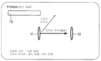
도 6은 Y=0㎜일 때의 평가계(10)에 대해 설명하기 위한 평면도이다.
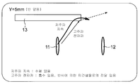
도 7은 Y=5㎜일 때의 평가계(10)에 대해 설명하기 위한 평면도이다.
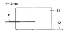
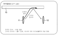
도 8은 Y=10㎜일 때의 평가계(10)에 대해 설명하기 위한 평면도이다.
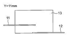
도 9는 Y=11㎜일 때의 평가계(10)에 대해 설명하기 위한 평면도이다.
도 10은 Y=15㎜일 때의 평가계(10)에 대해 설명하기 위한 평면도이다.
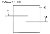
도 11은 Y=30㎜일 때의 평가계(10)에 대해 설명하기 위한 평면도이다.
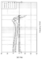
도 12는 평가계(10)에 있어서의 내부감 결합(Rda)의 시뮬레이션 결과를 나타내는 그래프이다.
도 13은 평가계(10)에 있어서 Y=0㎜일 때의 저주파 자속 및 고주파 전자파의 전파에 대해 설명하기 위한 도면이다.
도 14는 평가계(10)에 있어서 Y=5㎜일 때의 저주파 자속 및 고주파 전자파의 전파에 대해 설명하기 위한 도면이다.
도 15는 평가계(10)에 있어서 Y=10㎜일 때의 저주파 자속 및 고주파 전자파의 전파에 대해 설명하기 위한 도면이다.
도 16은 평가계(10)에 있어서 Y=30㎜일 때의 저주파 자속 및 고주파 전자파의 전파에 대해 설명하기 위한 도면이다.
도 17은 간섭물(2), 피간섭물(3)이 배선일 때의 전자 장치(1)의 케이스(5) 내부에 있어서의, 간섭물(2), 피간섭물(3), 전자 간섭 억제체(6)의 위치 관계에 대해 설명하기 위한 사시도이다.
도 18은 피간섭물(3)을 따라서 전자 간섭 억제체(21)를 배치한 전자 장치(20)의 단면을 나타낸 모식도이다.
도 19는 케이스(5)의 내측의 면을 따라서 배치한 전자 간섭 억제체(11)와, 그 전자 간섭 억제체(11)에 대향하도록 케이스(5)의 외측의 면을 따라서 배치한 도체판(31)을 구비하는 전자 장치(30)의 단면을 나타낸 모식도이다.
도 20은 케이스(5) 내측의 면을 따라서 배치한 전자 간섭 억제체(11)와, 그 전자 간섭 억제체(11)의 케이스(5) 외측의 면을 따라서 배치한 안테나(42)를 구비하는 전자 장치(40)의 단면을 나타낸 모식도이다.
도 21은 간섭물(2)을 배치한 기판(4A)과, 피간섭물(3)을 배치한 기판(4B)을 별개로 구비하는 전자 장치(50)의 단면을 나타낸 모식도이다.
도 22는 기판(4) 위에 배치한 간섭물(2)을 절연체(61)로 덮고, 그 위에 판 형상의 전자 간섭 억제체(62)를 배치한 전자 장치(60)의 부분 단면을 나타낸 모식도이다.
도 23은 기판(4) 위에 배치한 간섭물(2)을 절연체(61)로 덮고, 그 위를 추가로 전자 간섭 억제체(71)로 덮은 전자 장치(70)의 부분 단면을 나타낸 모식도이다.
도 24는 유연성을 가지는 시트형상의 전자 간섭 억제체(71)의 예와, 그 단면의 모식도이다.FIG. 1 is a schematic diagram showing a cross section of an
2 is a perspective view for explaining the positional relationship of the
3 is a perspective view for describing the
Fig. 4 is a plan view for explaining the Y coordinate in the
5 is a plan view for explaining the
6 is a plan view for explaining the
7 is a plan view for explaining the
8 is a plan view for explaining the
9 is a plan view for explaining the
10 is a plan view for explaining the
11 is a plan view for explaining the
12 is a graph showing a simulation result of the internal decoupling (Rda) in the
13 is a diagram for explaining the propagation of a low-frequency magnetic flux and a high-frequency electromagnetic wave when Y = 0 mm in the
Fig. 14 is a view for explaining the propagation of the low-frequency magnetic flux and the high-frequency electromagnetic wave when Y = 5 mm in the
15 is a diagram for explaining the propagation of a low-frequency magnetic flux and a high-frequency electromagnetic wave when Y = 10 mm in the
16 is a view for explaining the propagation of the low-frequency magnetic flux and the high-frequency electromagnetic wave when Y = 30 mm in the
Fig. 17 is a graph showing the relationship between the
18 is a schematic diagram showing a cross section of the
19 shows the
20 shows an
21 is a schematic diagram showing a cross section of an
22 is a schematic diagram showing a partial cross-sectional view of an
23 is a schematic view showing a partial cross-section of an
Fig. 24 is a schematic view showing an example of a sheet-shaped
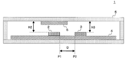
[0025] 본 발명의 제1 실시형태인 전자 장치(1)에 대해 도 1을 참조하여 설명한다. 전자 장치(1)는, 간섭물(2), 피간섭물(3), 기판(4), 케이스(5), 전자 간섭 억제체(6)를 구비한다. 전자 장치(1)는 임의의 종류의 전자 장치이다. 구체적으로는, 예컨대, 휴대 전화 단말 등의 통신 단말 장치, 데이터 통신 장치, 퍼스널 컴퓨터 등이 생각되지만, 이들로 한정되는 것은 아니고, 간섭물(2) 및 피간섭물(3)을 구비하는 것이면 어떠한 종류의 전자 장치라도 해당한다. 간섭물(2)은 노이즈를 발생할 우려가 있는 부품, 회로, 장치, 배선 등이다. 피간섭물(3)은 노이즈의 영향을 받을 우려가 있는 부품, 회로, 장치, 배선 등이며, 특히 대표적인 것으로서 안테나가 있다. 간섭물(2) 및 피간섭물(3)은 기판(4) 위에 배치된다. 간섭물(2), 피간섭물(3), 기판(4)은 케이스(5) 내에 수납된다. 케이스(5)의 내측, 간섭물(2)과 대면하는 위치에, 전자 간섭 억제체(6)가 배치된다. 케이스(5)는 예컨대 플라스틱 등의 절연체로 이루어진다.An
[0026] 또한, 전자 장치(1)는, 간섭물(2), 피간섭물(3) 이외의 부품, 회로, 장치, 배선 등을 기판(4) 상에 구비하는 것으로 해도 된다. 또, 전자 장치(1)는, 케이스(5)의 내부에 혹은 외부에, 간섭물(2), 피간섭물(3) 이외의 부품, 회로, 장치, 배선 등을 구비하는 것으로 해도 된다. 전자 간섭 억제체(6)는, 주로 소형 디지털 기기에서의 복사 노이즈 대책이나, 내부 간섭(자가 중독) 대책으로 사용되고 있다. 전자 간섭 억제체(6)로서는, 자성체 분말을 결합제 내에 분산시킨 시트형상의 부품, 보다 구체적으로는, 연자성 금속 분말을 절연성의 모재(母材) 내에 분산하여 이루어지는 시트형상의 부품이 고려된다. 혹은, 전자 간섭 억제체(6)는, 고저항의 자성체로 이루어진 후막(厚膜) 내지 박막(薄膜)이어도 된다. 또, 전자 간섭 억제체(6)의 형상은, 단순한 직사각형(矩形狀)의 시트여도 되지만, 전자 간섭을 억제하는 효과를 높이기 위하여, 직사각형의 시트에 슬릿을 형성한 것으로 해도 된다.The
[0027] 전자 간섭 억제체(6)는 간섭물(2)을 따라서 배치되어 있다. 바꾸어 말하면, 간섭물(2)을 따라서, 전자 간섭 억제체(6)와, 케이스(5)의 일부가 배치되어 있다. 전자 간섭 억제체(6)의 일단(一端)은, 간섭물(2)과 피간섭물(3)의 사이에 위치하고, 피간섭물(3) 위까지는 도달하지 않은 점에 주의해야 한다. 피간섭물(3) 위를 따라서 케이스(5)의 일부, 즉 절연체가 배치되어 있으나, 전자 간섭 억제체(6)는 배치되어 있지 않다. 도 1에 나타낸 바와 같이, 간섭물(2)의 단부로서 피간섭물(3)에 대향하는 것을 제1 단부(P1)로 한다. 피간섭물(3)의 단부로서 간섭물에 대향하는 단부를 제2 단부(P2)로 한다. 이때, 전자 간섭 억제체(6)의 일방(一方)의 단부는, 제1 단부(P1)와 제2 단부(P2)의 사이에 배치된다. 거리(D)는 제1 단부(P1)와 제2 단부(P2) 사이의 거리이다.The electromagnetic interference suppressor 6 is disposed along the
[0028] 이와 같이 전자 간섭 억제체(6)를 간섭물(2) 위만 덮고, 피간섭물(3)은 덮지 않도록 배치함으로써, 전자 간섭 억제체(6)의 면내 방향(도 1의 수평방향)으로 유기되는 전계를, 간섭물(2)과 피간섭물(3) 사이의 위치에서 분단할 수가 있다. 이 때문에, 전자 간섭 억제체(6)의 부작용인, 간섭물과 피간섭물 사이의 전자적 결합의 증가를 회피하면서, 넓은 주파수 대역에서 전자 간섭을 억제할 수가 있다.In the in-plane direction (the horizontal direction in FIG. 1) of the electromagnetic interference suppressor 6, by arranging the electromagnetic interference suppressor 6 only on the
[0029] 간섭물(2), 피간섭물(3)과 전자 간섭 억제체(6) 간의 위치 관계를 사시도로 나타낸 것이 도 2이다. 도 2에서는 케이스(5)는 생략되어 있다. 도 2에 있어서, Y방향은, 간섭물(2)과 피간섭물(3) 사이의 거리(D)에 해당하는 선분을 연장한 직선의 방향이며, X방향은 도면 중의 수평면 내에 있어서 Y방향에 직교하는 방향이다. Z방향은 수평면에 직교하는 방향이다. 전자 간섭 억제체(6)는, Z방향에서 볼 때 간섭물(2)의 전체 둘레를 덮고, 또한, Y방향에 대해서는 피간섭물(3)까지는 닿지 않도록, 간섭물(2)의 주변을 덮는다.FIG. 2 is a perspective view showing the positional relationship between the
[0030] 간섭물(2)의 상면과 케이스(5)의 하면 사이의 거리를 거리(H2)로 한다. 피간섭물(3)의 상면과 케이스(5)의 하면 사이의 거리를 거리(H3)로 한다. 이때, 거리(D, H2, H3)는, 전자 장치(1), 간섭물(2), 피간섭물(3) 등의 크기에 따라 다르다. 예컨대, 전자 장치(1)가 데스크 탑형 퍼스널 컴퓨터(PC)인 경우, 거리(D)를 5~300㎜로 하고, 거리(H2, H3)를 1~5㎜로 하는 것이 고려된다. 전자 장치(1)가 휴대 전화 단말 등의 휴대 기기인 경우, 위에서 기술한 데스크 탑형 PC의 거리(D, H2, H3)를 각각 1/3~1/5로 축소한 길이로 하는 것이 고려된다.The distance between the upper surface of the
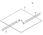
[0031] 전자 장치(1)를 모의(模擬)한 평가계로서, 도 3과 같은 평가계(10)를 모델화하였다. 평가계(10)에 대해, 안시스·재팬 가부시키가이샤의 고주파 3차원 전자계 해석 소프트웨어 ANSYS HFSS를 이용해 내부감 결합(Rda)을 계산하였다. 평가계(10)에 있어서, 2세트의 안테나(11, 12)는 루프 코일이며, 일방(一方)은 간섭물(2)에 대응하고, 타방(他方)은 피간섭물(3)에 대응한다. 안테나(11, 12)를 각각 도시되지 않은 네트워크 애널라이저의 포트(1), 포트(2)에 접속하고, 그 투과 특성(S21)에 근거하여 안테나(11, 12) 간의 결합을 평가하였다. 평가하는 파라미터인 내부감 결합(Rda)은 안테나 간의 결합도를 나타내는 지표이며, 값이 클수록 결합이 약함을 나타낸다. 즉, 내부감 결합(Rda)의 값이 클수록 전자 간섭 억제체(13)에 의해 노이즈의 전파가 억제되고 있음을 나타낸다. 내부감 결합(Rda)은 다음 식에 의해 구한다.As an evaluation system simulating the
Rda=S21R-S21MRda = S21R-S21M
여기서, S21R은 전자 간섭 억제체(13)가 없는 경우의 S파라미터이다. S21M은 전자 간섭 억제체(13)가 있는 경우의 S파라미터이다. 전자 간섭 억제체(13)는 전자 간섭 억제체(6)에 대응한다. 전자 간섭 억제체(13)는, Si 9.8%-Al 6.0%-Fe 조성(질량%)의 연자성 금속 분말을 편평화하고, 분말 충전성이 뛰어난 엘라스토머 내에 분산시켜, 두께가 0.2㎜인 전자 간섭 억제체이다. 안테나(11, 12)는 각각 1㎜의 두께를 갖는다. 안테나(11, 12) 사이의 거리는 위에서 기술한 거리(D)에 대응하며, 그 길이는 10㎜이다.Here, S21R is an S parameter when the
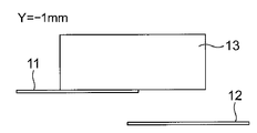
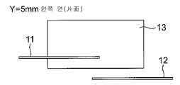
[0032] 전자 간섭 억제체(13)의 위치를 Y로 나타낸다. 도 4에 나타낸 바와 같이, Y는 안테나(11)에 대해서 직교하는 방향으로 연장되는 직선을 축으로 하는 좌표이며, 안테나(11)의 2면 중, 안테나(12)에 대향하는 쪽의 면을 제로로 하고, 안테나(12)에 가까워지는 방향을 플러스로 한다. 여기에서는, 도 5~도 11에 나타낸 바와 같이, 전자 간섭 억제체(13)가 Y=-1㎜, 0㎜, 5㎜, 10㎜, 11㎜, 15㎜, 30㎜의 위치에 있을 때의 내부감 결합(Rda)을 각각 시뮬레이션하였다. 또한, 본 시뮬레이션은, 안테나(11, 12)의 어느 쪽을 간섭물로 해도 마찬가지로 성립된다.The position of the
[0033] 내부감 결합(Rda)의 시뮬레이션 결과에 대해 도 12를 참조하여 설명한다.The simulation results of the internal decoupling (Rda) will be described with reference to FIG.
[0034] Y=-1㎜, 즉 전자 간섭 억제체(13)가 안테나(11)의 앞의 영역(도면 중, 안테나(11)보다 위인 영역)만 덮고, 안테나(11, 12) 중 어느 것도 덮지 않는 경우, Rda≒이며, 거의 효과가 없다.In the case where Y = -1 mm, that is, the
[0035] Y=0㎜, 즉 전자 간섭 억제체(13)가, 안테나(11)의 앞의 영역과, 안테나(11)의 바로 위(直上)를 덮는 경우, 시뮬레이션한 전체 주파수 대역에 걸쳐 Rda는 플러스가 되었다.When Y = 0 mm, that is, when the
[0036] Y=0㎜일 때, 도 13에 나타낸 바와 같이, 간섭물이 발생시키는 저주파 자속(磁束)은, 전자 간섭 억제체에 의해 수렴(集束)되는 일 없이, 피간섭물에 직진하는 것으로 생각된다. 한편, 간섭물이 발생시키는 고주파 전자파는, 전자 간섭 억제체에 의해 흡수되는 경우도 반사되는 경우도 없다고 생각된다.When Y = 0 mm, as shown in FIG. 13, the low-frequency magnetic flux generated by the interference does not converge (converge) by the electromagnetic interference suppressor and goes straight to the interference I think. On the other hand, it is considered that the high-frequency electromagnetic wave generated by the interference does not get absorbed or reflected by the electromagnetic interference suppressor.
[0037] Y=5㎜, 즉, 안테나(11)의 앞의 영역에 추가하여, 안테나(11)의 바로 위, 그리고, 안테나(11)로부터 폭 5㎜의 영역을 덮을 경우, 시뮬레이션한 전체 주파수 대역에 걸쳐 Rda는 플러스이며, 또한, 2㎓ 부근의 일부를 제외하고, Y=0㎜일 때보다 Rda는 컸다.When Y = 5 mm, that is, an area immediately before the
[0038] Y=5㎜일 때, 도 14에 나타낸 바와 같이, 간섭물이 발생시키는 저주파 자속은, 전자 간섭 억제체에 의해 수렴되는 것으로 생각된다. 간섭물이 발생시키는 고주파 전자파는, 전자 간섭 억제체에 의해 일부가 흡수되고, 일부가 반사되는데, 반사한 고주파 전자파는 피간섭물로부터 어긋난 방향을 향하는 것으로 생각된다.When Y = 5 mm, as shown in FIG. 14, it is considered that the low-frequency magnetic flux generated by the interference is converged by the electromagnetic interference suppressor. The high-frequency electromagnetic wave generated by the interference is partially absorbed by the electromagnetic interference suppressor and partially reflected. The reflected high-frequency electromagnetic wave is considered to be deviated from the interference.
[0039] Y=10㎜, 즉, 안테나(11)의 앞의 영역으로부터, 안테나(12)의 바로 앞(안테나(12)의 바로 위를 포함하지 않음)까지 덮을 경우, 약 2.5㎓까지는 Y=5㎜인 경우보다 Rda는 크지만, 약 2.5㎓에서 역전(逆轉)하고, 2.775㎓에서 Rda는 제로를 통과해 마이너스가 된다. 단, 후술하는 Y=11m, 15㎜, 30㎜인 경우에 비해, 고주파 영역에서의 하락은 작다. 3㎓일 때 Rda는 -1.5dB이다.When Y = 10 mm, that is, from the front area of the
[0040] Y=10㎜일 때, 도 15에 나타낸 바와 같이, 간섭물이 발생시키는 저주파 자속은, 전자 간섭 억제체에 의해 수렴되는 것으로 생각된다. 간섭물이 발생시키는 고주파 전자파는, 전자 간섭 억제체에 의해 일부가 흡수되고, 일부가 반사된다. 반사된 고주파 전자파는 피간섭물에도 전달되는 것으로 생각된다.When Y = 10 mm, as shown in FIG. 15, it is considered that the low-frequency magnetic flux generated by the interference is converged by the electromagnetic interference suppressor. The high frequency electromagnetic wave generated by the interference is partially absorbed by the electromagnetic interference suppressor and partially reflected. The reflected high frequency electromagnetic wave is considered to be transmitted to the interference.
[0041] Y=11㎜, 즉, 안테나(11)의 앞의 영역으로부터, 안테나(12)의 바로 위까지 덮는 경우, 약 2.4㎓까지는 Rda는 플러스이며, 여기서부터 앞이면 Rda는 마이너스이다. 3㎓일 때 Rda는 -5.0dB이다.In the case of Y = 11 mm, that is, covering from the area in front of the
[0042] Y=15㎜, 즉, 안테나(11)의 앞의 영역으로부터, 안테나(12)의 바로 위를 통과하고, 나아가 폭 4㎜의 영역을 덮을 경우, 약 2.16㎓에서 플러스로부터 마이너스로 변한다. 3㎓일 때 Rda는 -6.0dB이다.When Y = 15 mm, that is, the region passing directly above the
[0043] Y=30㎜, 즉, 안테나(11)의 앞의 영역으로부터, 안테나(12)의 바로 위를 통과하고, 나아가 폭 19㎜의 영역을 덮을 경우, 약 2.43㎓에서 플러스로부터 마이너스로 변한다. 3㎓일 때 Rda는 -5.1dB이다.When Y = 30 mm, that is, the area passing the
[0044] Y=30㎜일 때, 위에서 기술한 Y=10㎜일 때와 마찬가지로, 도 16에 나타낸 바와 같이, 간섭물이 발생시키는 저주파 자속은, 전자 간섭 억제체에 의해 수렴되는 것으로 생각된다. 간섭물이 발생시키는 고주파 전자파는, 전자 간섭 억제체에 의해 일부가 흡수되고, 일부가 반사된다. 반사된 고주파 전자파는 피간섭물에도 전달되는 것으로 생각된다.When Y = 30 mm, as in the case of Y = 10 mm described above, it is considered that the low-frequency magnetic flux generated by the interference is converged by the electromagnetic interference suppressor as shown in FIG. The high frequency electromagnetic wave generated by the interference is partially absorbed by the electromagnetic interference suppressor and partially reflected. The reflected high frequency electromagnetic wave is considered to be transmitted to the interference.
[0045] 이상과 같은 시뮬레이션 결과로부터, 내부감 결합(Rda)이 마이너스로 변하는 것, 즉, 안테나(11, 12) 사이의 전자 결합의 증가를 억제하려면, Y=0~10㎜로 하는 것이 바람직함을 알 수 있다. 이는 즉, 전자 간섭 억제체(13)가 안테나(11) 위를 통과하여, 안테나(12)의 바로 앞(直前)까지 덮는 상태이다.From the above simulation results, it is preferable that Y = 0 to 10 mm in order to suppress the internal decoupling Rda to be negative, that is, to suppress the increase of the electromagnetic coupling between the
[0046] 특히, 5≤Y≤10인 경우, 2㎓ 이상의 주파수 대역이어도 내부감 결합(Rda)이 마이너스가 되는 구간이 작고, 또한, 비교적 낮은 주파수대여도 비교적 큰 내부감 결합(Rda)이 얻어진다는 점에서 바람직하다. 또, 2㎓ 이상의 주파수 대역을 포함하는 전체 주파수 대역에서 내부감 결합(Rda)이 플러스인 것을 중시하는 경우에는, Y=5㎜로 하면 내부감 결합(Rda)이 커지므로 바람직하다.Particularly, in the case of 5? Y? 10, even in the frequency band of 2 GHz or more, the interval in which the internal decoupling Rda becomes negative is small and the internal decoupling Rda is relatively large, . In the case of emphasizing that the internal decoupling Rda is positive in the entire frequency band including the frequency band of 2 GHz or more, it is preferable that Y = 5 mm because the internal decoupling Rda becomes large.
[0047] 전자 장치(1)에 의하면, 그 내부에서 발생하는 전자 간섭을 광대역에서 억제할 수가 있다. 이 때문에, 내장하는 전자 회로의 고속화나 소형화가 용이해진다. 또, 전자 장치(1)가 통신 장치인 경우, 통신 품질의 확보가 용이해진다.According to the
[0048] 이하에, 전자 장치(1)의 여러 가지 변형에 대해 설명한다.Hereinafter, various modifications of the
[0049] 위에서 기술한 도 2에서는, 간섭물(2), 피간섭물(3)이 기판(4) 상에 배치되는 소형의 부품인 것을 전제로 하여 나타내었으나, 간섭물(2), 피간섭물(3)은 배선이어도 된다. 이때 간섭물(2), 피간섭물(3), 전자 간섭 억제체(6)의 배치는 도 17과 같게 된다. 이때에도 위에서 기술한 전자 장치(1)에 대한 설명이 거의 그대로 적용될 수 있음은 당업자에게는 분명한 일일 것이다.In the above-described FIG. 2, it is assumed that the
[0050] 도 18을 참조하여 전자 장치(20)에 대해 설명한다. 전자 장치(20)에서는 전자 간섭 억제체(21)의 위치가 전자 장치(1)와는 다르다. 전자 장치(1)에서는, 간섭물(2) 위를 덮도록 전자 간섭 억제체(6)를 배치했던 것에 대하여, 전자 장치(20)에서는, 피간섭물(3) 위를 덮도록 전자 간섭 억제체(21)를 배치하고 있다. 전자 장치(20)에서는 간섭물(2) 위에는 전자 간섭 억제체는 배치되어 있지 않다.[0050] The
[0051] 본 발명에서는, 전자 간섭 억제체에 의해 반사된 고주파 전자파가 피간섭물(3)에 닿는 것을 회피하기 위하여, 간섭물(2), 피간섭물(3) 중의 어느 일방(一方)만을 덮도록 하여 전자 간섭 억제체를 배치한다. 전자 장치(1)와 같이 간섭물(2)을 덮도록 전자 간섭 억제체를 배치해도 되고, 혹은, 전자 장치(20)와 같이 피간섭물(3)만 덮도록 배치해도 된다. 이하에 설명하는 변형예에서는, 전자 간섭 억제체를 간섭물, 피간섭물 중의 어느 일방만 덮도록 배치한 것을 들어 설명하고 있지만, 전자 간섭 억제체에 의해 반사된 고주파 전자파에 의한 영향을 막는 효과에 대해 말하자면, 타방(他方)만 덮도록 해도 마찬가지의 효과를 얻을 수 있다.In the present invention, in order to avoid the high frequency electromagnetic wave reflected by the electromagnetic interference suppressor from touching the
[0052] 도 19의 전자 장치(30)는, 케이스(5)의 내측의 면을 따라서 배치한 전자 간섭 억제체(11)를 구비하고, 추가로, 그 전자 간섭 억제체(11)에 대향하도록 케이스(5)의 외측의 면을 따라서 배치한 도체판(31)을 구비한다. 피간섭물(3)에서 볼 때, 도체판(31)은 전자 간섭 억제체(11)에 가려지도록 배치된다. 이 때문에, 도체판(31)의 바닥면은 전자 간섭 억제체(11)의 바닥면과 같거나 그것보다 작은 것으로 한다. 도체판(31)은 케이스(5)의 외부로부터 피간섭물(3)로 비래(飛來)하는 전자파에 대한 전자 실드로서 기능한다. 또한, 전자 장치(30)에서는, 케이스(5) 위에 도체판(31)을 배치하고 있지만, 케이스(5) 중, 전자 간섭 억제체(11)의 배면에 해당되는 위치에 개구를 형성하고, 그 개구 내에 도체판(31)을 매립하도록 배치해도 된다. 반사에 의한 노이즈의 전달을 막는다는 관점에서는, 도체판(31)은 보다 작은 편이 바람직하다.The
[0053] 도 20의 전자 장치(40)는, 케이스(5) 중, 전자 간섭 억제체(11)의 배면에 해당되는 위치에, 오목부(41)를 형성하고, 그 안에 안테나(42)를 배치한 것이다. 전자 장치(40)는 휴대 전화 단말 등의 무선 통신 단말이며, 안테나(42)는 무선 통신을 위한 안테나이다.The
[0054] 도 21의 전자 장치(50)는, 전자 장치(1)에 있어서의 한 장의 기판(4) 대신에, 2매의 기판(4A, 4B)을 설치하고, 각각에 간섭물(2), 피간섭물(3)을 배치한 것이다. 이와 같이, 간섭물(2), 피간섭물(3)을 반드시 동일한 기판상에 배치할 필요는 없으며, 각각을 다른 기판상에 배치하는 것으로 해도 본 발명은 성립된다.The
[0055] 위에서 기술한 전자 장치(1)나, 그 변형인 전자 장치(20, 30, 40, 50)에서는, 전자 간섭 억제체를 케이스의 내면에 붙인 것으로 하여 설명하였다. 그러나, 본 발명의 효과는, 간섭물, 피간섭물 및 전자 간섭 억제체의 위치 관계에 의해 생기는 것이기 때문에, 전자 간섭 억제체를 지지하는 지지체는, 반드시 케이스일 필요는 없다. 예컨대, 간섭물의 주위의 네 모서리에 지지 기둥을 설치하고, 그 지지 기둥으로 전자 간섭 억제체를 지지하는 구조로 해도 된다. 이러한 구조에서는, 전자 간섭 억제체는 케이스로부터 떨어진 위치에서 지지되는 경우도 있다.The
[0056] 본 발명의 제2 실시형태인 전자 장치(60)에 대해 설명한다. 위에서 기술한 제1 실시형태에서는, 전자 간섭 억제체는 케이스의 내면을 따라서 배치되었다. 또, 케이스는 원칙적으로는 절연체이지만, 전자 간섭 억제체의 케이스 외측에 대해서는 도체로 할 수도 있었다. 이에 대하여, 제2 실시형태에서는, 기판상의 간섭물 및 피간섭물 중, 적어도 어느 일방을, 절연체로 덮는 것으로 하고 있다. 또, 그 절연체로 덮은 간섭물/피간섭물의 절연체의 더 외측 중, 적어도 상면을 전자 간섭 억제체로 덮는 것으로 하고 있다. 제1 실시형태에 관하여, 도 3~16을 참조하여 평가계(10)에 대해 설명하였으나, 이 설명은 제2 실시형태에 대해서도 마찬가지로 적용된다.An
[0057] 도 22에 나타낸 바와 같이, 전자 장치(60)에서는, 기판(4) 위에 배치한 간섭물(2)을 절연체(61)로 덮고, 그 위에 판 형상의 전자 간섭 억제체(62)를 배치하고 있다. 절연체(61)는 예컨대 몰드 수지이다. 전자 간섭 억제체(62)는, 절연체(61)로 덮인 간섭물(2)의 상면을 모두 덮고 있지만, 측면은 덮지 않았다. 도시된 케이스(63)는 전자 장치(60)의 일부이다. 도 22에 도시되어 있는 것은 케이스(63)의 일부이며, 좌우 단부(端部)의 물결선의 전방에는 케이스(63)의 도시되지 않은 부분이 계속되고 있다. 케이스(63)에는, 전자 간섭 억제체를 배치한 부분 이외에는 절연체라는 제약은 없으며, 전체가 금속으로 이루어진 케이스여도 된다. 이는 간섭물(2)을 절연체(61)로 덮고 있기 때문에, 금속 케이스에 의한 노이즈 반사가 발생하지 않기 때문이다.22, in the
[0058] 전자 장치(60)의 변형인 전자 장치(70)에서는, 도 23에 나타낸 바와 같이, 기판(4) 위에 배치한 간섭물(2)을 절연체(61)로 덮고 있는 점에서는 전자 장치(60)와 같다. 전자 장치(60)에서는, 전자 간섭 억제체(62)는 판 형상이며, 절연체(61)를 사이에 두고 간섭물(2) 위에 전자 간섭 억제체(62)를 재치한 구조를 가지고 있다. 이에 대해서, 전자 장치(70)에서는, 전자 간섭 억제체(71)는, 유연성을 가지는 시트형상이며, 절연체(61)의 상면 및 측면의 전체 둘레를 덮고, 나아가, 그 주변의 기판(4)의 표면도 덮고 있다.In the
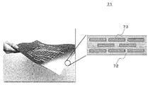
[0059] 도 24에 나타낸 바와 같이, 전자 간섭 억제체(71)는, 예컨대 수지(72)로 이루어진 시트에, 자성 편평 분말(73)을 층 형상으로 분포시킨 것이다. 전자 간섭 억제체(71)는 제1 실시형태의 전자 간섭 억제체(6, 13, 21)나, 전자 장치(60)의 전자 간섭 억제체(62)로서도 이용할 수 있다. 또, 도 24에 도시한 것은 전자 간섭 억제체의 일례이며, 전자 간섭 억제체(71)와 다른 구성의 것을 이용해도 된다.As shown in FIG. 24, the
[0060] 수지(72)는 예컨대 아크릴 고무, 염소화 폴리에틸렌, 폴리부타디엔, 폴리이소프로필렌, EPM, EPDM, SBR, 니트릴 고무, 에피클로로히드린, 네오프렌, 부틸, 폴리설파이드, 우레탄 고무 등의 엘라스토머·고무, 폴리에틸렌, 폴리프로필렌, 폴리스티렌, 아크릴, 폴리염화비닐, 폴리카보네이트, 나일론, 우레탄, PBT, PET, ABS등의 열가소성 수지, 멜라민, 페놀, 에폭시, 우레탄, 폴리이미드, 디알릴프탈레이트, 불포화 폴리에스테르, 푸란 등의 열경화성 수지이다. 자성 편평 분말(73)은 예컨대 철계 비정질 합금으로 이루어진 편평 형상의 연자성 입자이다.The
[0061] 전자 장치(70)에서는, 간섭물(2)의 상면뿐만 아니라, 측면에 대해서도 전자 간섭 억제체(71)에 의해 덮으므로, 예컨대 간섭물(2)의 높이가 높은 경우라 하더라도 효과적으로 노이즈를 억제할 수가 있다.In the
[0062] 또한, 전자 장치(60, 70)에서는, 간섭물(2)을 덮는 절연체(61, 62) 위에 전자 간섭 억제체(62, 72)를 배치했지만, 간섭물(2) 대신에 피간섭물(3)을 절연체로 덮고, 그 위에 전자 간섭 억제체를 배치하는 것으로 해도 된다.In the
[0063] 또, 전자 장치(60, 70)에서는, 기판(4) 위에 배치한 간섭물(2)의 위부터 절연체(61)로 덮는 구조를 가지고 있지만, 배선 등의 일부를 제외한 간섭물(2)의 전체를 미리 절연체(61)로 덮은 후에 기판(4) 위에 배치하는 것으로 해도 된다.The
[0064] 또, 전자 장치(70)에서는, 절연체(61)로 덮은 간섭물(2)을, 그 주변의 기판(4)과 함께 전자 간섭 억제체(71)로 덮는 구조로 하고 있지만, 절연체(61)로 덮인 간섭물(2)을, 미리 전자 간섭 억제체(71)로 덮고, 그 후에, 기판(4)에 배치하는 구조로 해도 된다.The
[0065] 또, 제1 실시형태의 변형과 제2 실시형태를 적절히 조합할 수 있음은 당업자라면 이해할 수 있을 것이다. 예컨대, 도 21의 전자 장치(50)와 같이, 절연체(61), 전자 간섭 억제체(62 또는 71)로 덮은 간섭물(2)과 피간섭물(3)을, 각각 다른 기판상에 배치해도 됨은 당업자에게는 자명한 일일 것이다.[0065] It will be understood by those skilled in the art that the modification of the first embodiment and the second embodiment can be appropriately combined. For example, even when the
[0066] 1, 20, 30, 40, 50, 60, 70; 전자 장치
2; 간섭물
3; 피간섭물
4, 4A, 4B; 기판
5, 63; 케이스
6, 13, 21, 62, 71; 전자 간섭 억제체
10; 평가계
11, 12, 42; 안테나
31; 도체판
41; 오목부
61; 절연체
72; 수지
73; 자성 편평 분말[0066] 1, 20, 30, 40, 50, 60, 70; Electronic device
2; Interference
3; Interference
4, 4A, 4B; Board
5, 63; case
6, 13, 21, 62, 71; Electromagnetic interference suppressor
10; Evaluation system
11, 12, 42; antenna
31; Conductor plate
41; Concave portion
61; Insulator
72; Suzy
73; Magnetic flat powder
Claims (12)
전자파의 영향을 받는 피(被)간섭물,
상기 간섭물 및 상기 피간섭물을 재치(載置)하기 위한 기판,
상기 간섭물 및 상기 피간섭물 중의 어느 일방(一方)만을 따라서, 상기 기판과 평행하게 배치된 전자 간섭 억제체를 구비하고,
상기 간섭물의 단부(端部)로서 상기 피간섭물에 대향하는 것을 제1 단부로 하고, 상기 피간섭물의 단부로서 상기 간섭물에 대향하는 단부를 제2 단부로 할 때, 상기 전자 간섭 억제체의 일방의 단부는, 상기 제1 단부와 상기 제2 단부의 사이에 배치되는
전자 장치.An interference that generates electromagnetic waves,
The interference caused by electromagnetic waves,
A substrate for placing the interference and the object to be interposed,
And an electromagnetic interference suppressor arranged parallel to said substrate only on at least one of said interference and said interference,
Wherein when an end portion of the interference object is a first end that faces the object to be intercepted and an end portion of the object to be intercepted as the end portion of the interfered object is a second end portion, One end portion is disposed between the first end portion and the second end portion
Electronic device.
상기 간섭물 및 피간섭물의 타방(他方)을 따라서 상기 기판과 평행하게 배치된 절연체를 더 구비하는
전자 장치.The method according to claim 1,
And an insulator disposed parallel to the substrate along the other of the interference and the interfered object
Electronic device.
상기 간섭물 및 상기 피간섭물의 양방(兩方)을 둘러싸는 케이스(筐體)를 구비하고, 상기 케이스는 상기 전자 간섭 억제체 및 상기 절연체를 구비하는
전자 장치.3. The method of claim 2,
And a case enclosing both of the interference and the interference, wherein the case includes the electromagnetic interference suppressor and the insulator
Electronic device.
상기 전자 간섭 억제체의 일방의 면을 따라서 상기 간섭물 및 상기 피간섭물 중의 어느 일방을 배치했을 때, 상기 전자 간섭 억제체의 타방의 면을 따라서 배치된 도체판을 구비하는
전자 장치.4. The method according to any one of claims 1 to 3,
And a conductor plate disposed along the other surface of the electromagnetic interference suppressor when either one of the interference and the interference is disposed along one surface of the electromagnetic interference suppressor
Electronic device.
상기 간섭물 및 상기 피간섭물은, 각각, 전자 부품, 전자 회로, 및 배선 중 어느 것인
전자 장치.5. The method according to any one of claims 1 to 4,
Wherein the interference and the interfered object are any one of an electronic part, an electronic circuit, and a wiring
Electronic device.
상기 간섭물은 전원선이며, 상기 피간섭물은 신호선인
전자 장치.6. The method of claim 5,
Wherein the interference is a power line, and the interference is a signal line
Electronic device.
서로 다른 제1 및 제2 기판을 포함하는 복수의 기판을 구비하고,
상기 간섭물은 상기 제1 기판에 배치되고, 상기 피간섭물은 상기 제2 기판에 배치되는
전자 장치.7. The method according to any one of claims 1 to 6,
A plurality of substrates including first and second substrates different from each other,
Wherein the interference is disposed on the first substrate, and the interference is disposed on the second substrate
Electronic device.
통신 장치.An electronic device as claimed in any one of claims 1 to 7,
Communication device.
전자파의 영향을 받는 피간섭물,
상기 간섭물 및 상기 피간섭물을 재치하기 위한 기판, 및,
상기 간섭물 및 상기 피간섭물 중의 어느 일방만을 따라서, 상기 기판과 평행하게 배치된 전자 간섭 억제체를 구비하는 전자 장치에,
상기 간섭물의 단부로서 상기 피간섭물에 대향하는 것을 제1 단부로 하고, 상기 피간섭물의 단부로서 상기 간섭물에 대향하는 단부를 제2 단부로 할 때, 상기 전자 간섭 억제체의 일방의 단부가, 상기 제1 단부와 상기 제2 단부의 사이에 위치하도록 배치하는,
전자 간섭 억제체의 배치방법.An interference that generates electromagnetic waves,
An object to be influenced by electromagnetic waves,
A substrate for placing the interference and the interference,
And an electromagnetic interference suppressor disposed parallel to said substrate along either one of said interference and said interference,
Wherein one end of the electromagnetic interference suppressor is an end portion of the electromagnetic interference suppressor, and the other end of the electromagnetic interference suppressor is an end portion of the electromagnetic interference suppressor The first end and the second end,
A method of disposing an electromagnetic interference suppressor.
전자파의 영향을 받는 피간섭물,
상기 간섭물 및 상기 피간섭물을 재치하기 위한 기판,
상기 간섭물 및 상기 피간섭물 중의 어느 일방의 일부 내지 전부를 덮는 절연체, 및,
상기 절연체에 의한 피복물에 상기 절연체를 사이에 두고 배치되는 전자 간섭 억제체
를 구비하는
전자 장치.An interference that generates electromagnetic waves,
An object to be influenced by electromagnetic waves,
A substrate for placing the interference and the interference,
An insulator covering at least a part of the one of the interference and the interference,
An electromagnetic interference suppressor disposed on the coating by the insulator with the insulator interposed therebetween;
Having a
Electronic device.
상기 전자 간섭 억제체는 판 형상이며, 상기 피복물 중, 상기 기판에 접하는 면에 대향하는 면을 덮도록 배치되는
전자 장치.11. The method of claim 10,
Wherein the electromagnetic interference suppressor is plate-shaped, and is disposed so as to cover a surface of the coating that faces the surface in contact with the substrate
Electronic device.
상기 전자 간섭 억제체는 시트 형상이며, 상기 피복물 중, 상기 기판에 접하는 면 이외의 면을 덮도록 배치되는
전자 장치.11. The method of claim 10,
Wherein the electromagnetic interference suppressor is sheet-shaped, and is disposed so as to cover a surface other than a surface in contact with the substrate,
Electronic device.
Applications Claiming Priority (3)
| Application Number | Priority Date | Filing Date | Title |
|---|---|---|---|
| JP2015254001A JP2017118015A (en) | 2015-12-25 | 2015-12-25 | Electronic device and method of arranging electromagnetic interference suppressor |
| JPJP-P-2015-254001 | 2015-12-25 | ||
| PCT/JP2016/065542 WO2017110113A1 (en) | 2015-12-25 | 2016-05-26 | Electronic device and method for disposing electromagnetic interference suppressor |
Publications (2)
| Publication Number | Publication Date |
|---|---|
| KR20180098368A true KR20180098368A (en) | 2018-09-03 |
| KR102441507B1 KR102441507B1 (en) | 2022-09-06 |
Family
ID=59089995
Family Applications (1)
| Application Number | Title | Priority Date | Filing Date |
|---|---|---|---|
| KR1020187021548A Active KR102441507B1 (en) | 2015-12-25 | 2016-05-26 | Disposition method of electronic device and electromagnetic interference suppressor |
Country Status (6)
| Country | Link |
|---|---|
| US (1) | US10729044B2 (en) |
| JP (1) | JP2017118015A (en) |
| KR (1) | KR102441507B1 (en) |
| CN (1) | CN108370655B (en) |
| TW (1) | TWI672092B (en) |
| WO (1) | WO2017110113A1 (en) |
Families Citing this family (19)
| Publication number | Priority date | Publication date | Assignee | Title |
|---|---|---|---|---|
| JP2018088029A (en) * | 2016-11-28 | 2018-06-07 | 富士通株式会社 | Electromagnetic noise countermeasure verification program, information processing apparatus, and electromagnetic noise countermeasure verification method |
| DE112017006387B4 (en) * | 2016-12-21 | 2024-07-11 | Mitsubishi Electric Corporation | SEMICONDUCTOR UNIT |
| CN109561642B (en) * | 2018-10-26 | 2020-07-31 | Oppo广东移动通信有限公司 | Electromagnetic interference control method and related product |
| CN109561643A (en) * | 2018-11-02 | 2019-04-02 | Oppo广东移动通信有限公司 | Electromagnetic interference control method and Related product |
| US11644425B2 (en) | 2019-07-19 | 2023-05-09 | Dell Products L.P. | System and method for optical state determination |
| US11399450B2 (en) | 2019-07-19 | 2022-07-26 | Dell Products L.P. | System and method for managing electromagnetic interference |
| US12004336B2 (en) | 2019-07-19 | 2024-06-04 | Dell Products L.P. | System and method for thermal management and electromagnetic interference management |
| US11234347B2 (en) | 2019-07-19 | 2022-01-25 | Dell Products L.P. | System and method for physical management of devices |
| US11132038B2 (en) | 2019-07-19 | 2021-09-28 | Dell Products L.P. | System and method for thermal management of shadowed devices |
| US11378608B2 (en) * | 2019-07-19 | 2022-07-05 | Dell Products L.P. | System and method for device state determination |
| US11122718B2 (en) | 2019-07-19 | 2021-09-14 | Dell Products L.P. | System and method for device level electromagnetic interference management |
| US11143682B2 (en) * | 2019-07-19 | 2021-10-12 | Dell Products L.P. | System and method for communicating externally from an electromagnetic interference suppressed volume |
| US11147194B2 (en) | 2019-08-21 | 2021-10-12 | Dell Products L.P. | System and method for managing electromagnetic interference |
| US11234350B2 (en) | 2019-08-21 | 2022-01-25 | Dell Products L.P. | System and method for isolated device access |
| TWI715306B (en) * | 2019-11-22 | 2021-01-01 | 英業達股份有限公司 | Set-up table |
| TWI727832B (en) * | 2020-06-17 | 2021-05-11 | 海華科技股份有限公司 | Wireless communication device |
| EP4220859A4 (en) * | 2020-09-28 | 2024-03-27 | FUJIFILM Corporation | Laminate manufacturing method, antenna-in package manufacturing method, laminate, and composition |
| US11925009B2 (en) * | 2021-03-09 | 2024-03-05 | Hamilton Sundstrand Corporation | Adaptive design and fabrication of radiation shielding inserts for electronic components |
| CN119716178A (en) * | 2024-12-13 | 2025-03-28 | 华北电力大学 | An anti-electromagnetic interference device and method for on-site inspection device of transformer monitoring device |
Citations (6)
| Publication number | Priority date | Publication date | Assignee | Title |
|---|---|---|---|---|
| JP2000196282A (en) | 1998-12-24 | 2000-07-14 | Tokin Corp | Electronic circuit device, mobile phone equipped with the same, and simple mobile phone |
| JP2001268190A (en) * | 2000-03-22 | 2001-09-28 | Sony Corp | Communication terminal device |
| JP2002185408A (en) * | 2000-12-11 | 2002-06-28 | Mitsubishi Electric Corp | Optical transceiver |
| JP2010135701A (en) * | 2008-12-08 | 2010-06-17 | Sony Corp | Electromagnetic wave suppression sheet, device and electronic apparatus |
| JP2011049807A (en) * | 2009-08-27 | 2011-03-10 | Kyocera Corp | Portable electronic equipment |
| KR20140057040A (en) | 2012-11-02 | 2014-05-12 | 연세대학교 산학협력단 | Compositions for improving skin aging comprising piperine compounds as active ingredients |
Family Cites Families (33)
| Publication number | Priority date | Publication date | Assignee | Title |
|---|---|---|---|---|
| FI113937B (en) * | 1989-02-21 | 2004-06-30 | Tatsuta Electric Wire & Gable | Printed circuit board and method for its production |
| JPH0810957Y2 (en) * | 1991-06-26 | 1996-03-29 | 鐘淵化学工業株式会社 | Anti-reflection structure for internal circuits of high frequency electronic devices |
| FI103935B1 (en) | 1994-09-07 | 1999-10-15 | Nokia Mobile Phones Ltd | A method for attaching an EMC protective cover to a circuit board and an EMC protective cover |
| JPH11354691A (en) * | 1998-06-10 | 1999-12-24 | Nec Corp | Integrated circuit device and mounting method thereof |
| JP2001274582A (en) * | 2000-03-23 | 2001-10-05 | Sony Corp | Electronics |
| JP2002134679A (en) * | 2000-10-25 | 2002-05-10 | Sony Corp | Integrated circuit |
| DE10233318C1 (en) * | 2002-07-22 | 2003-09-25 | Siemens Ag | Interference suppression device for electronic apparatus uses capacitor connected between plug element for apparatus circuit and housing potential |
| CN1810068A (en) * | 2003-06-19 | 2006-07-26 | 波零公司 | EMI absorbing shielding for printed circuit boards |
| JP2005235944A (en) * | 2004-02-18 | 2005-09-02 | Tdk Corp | Electronic device and manufacturing method thereof |
| JP4415322B2 (en) * | 2005-04-22 | 2010-02-17 | 日立金属株式会社 | Electronic circuit having antenna sealed with magnetic material |
| JP5216342B2 (en) * | 2008-01-29 | 2013-06-19 | 京セラ株式会社 | Shield case and electronic equipment |
| US8477499B2 (en) * | 2009-06-05 | 2013-07-02 | Laird Technologies, Inc. | Assemblies and methods for dissipating heat from handheld electronic devices |
| WO2011007570A1 (en) * | 2009-07-17 | 2011-01-20 | パナソニック株式会社 | Electronic module and method for manufacturing same |
| US8493749B2 (en) * | 2009-10-12 | 2013-07-23 | Apple Inc. | Conforming EMI shielding |
| CN102056448B (en) * | 2009-11-04 | 2013-02-27 | 环旭电子股份有限公司 | Electronic module |
| US8213180B2 (en) * | 2010-01-21 | 2012-07-03 | Broadcom Corporation | Electromagnetic interference shield with integrated heat sink |
| CN202014429U (en) * | 2011-04-27 | 2011-10-19 | 东莞宇龙通信科技有限公司 | Electronic device |
| WO2011137756A2 (en) * | 2011-05-06 | 2011-11-10 | 华为终端有限公司 | Composite material and electron device |
| CN102296274B (en) * | 2011-08-18 | 2013-11-27 | 北京镨玛泰克真空科技有限公司 | Shielding for cathodic arc metal ion sources |
| JP5693486B2 (en) * | 2012-02-14 | 2015-04-01 | 三菱電機株式会社 | High frequency circuit case cover, method for manufacturing the same, and high frequency circuit module using the same |
| JP6225436B2 (en) | 2012-08-16 | 2017-11-08 | 住友ベークライト株式会社 | Electromagnetic wave shielding film and method for coating electronic component |
| JPWO2014098065A1 (en) * | 2012-12-19 | 2017-01-12 | 戸田工業株式会社 | Electromagnetic interference suppressor |
| KR200486521Y1 (en) * | 2013-03-12 | 2018-05-30 | 네오그라프 솔루션즈, 엘엘씨 | Portable electronic device thermal management system |
| CN104347595B (en) * | 2013-07-31 | 2017-04-12 | 环旭电子股份有限公司 | Electronic packaging module and manufacturing method thereof |
| US9501112B2 (en) * | 2013-08-10 | 2016-11-22 | Intel Corporation | Thermal energy storage, dissipation and EMI suppression for integrated circuits using porous graphite sheets and phase change material |
| SG2013083258A (en) * | 2013-11-06 | 2015-06-29 | Thales Solutions Asia Pte Ltd | A guard structure for signal isolation |
| US9420734B2 (en) * | 2014-04-01 | 2016-08-16 | Advanced Micro Devices, Inc. | Combined electromagnetic shield and thermal management device |
| KR20150130915A (en) | 2014-05-14 | 2015-11-24 | 티디케이가부시기가이샤 | Magnetism suppressing sheet and manufacturing method thereof |
| JP2015220260A (en) * | 2014-05-14 | 2015-12-07 | Tdk株式会社 | Magnetism suppression sheet and method of manufacturing the same |
| US9820373B2 (en) * | 2014-06-26 | 2017-11-14 | Apple Inc. | Thermal solutions for system-in-package assemblies in portable electronic devices |
| US9357683B2 (en) * | 2014-09-26 | 2016-05-31 | Laird Technologies, Inc. | Electromagnetic interference (EMI) shielding apparatus including electrically-conductive foam |
| CN204632754U (en) * | 2015-03-18 | 2015-09-09 | 新科实业有限公司 | Electronic component module |
| US9781819B2 (en) * | 2015-07-31 | 2017-10-03 | Laird Technologies, Inc. | Multifunctional components for electronic devices and related methods of providing thermal management and board level shielding |
-
2015
- 2015-12-25 JP JP2015254001A patent/JP2017118015A/en active Pending
-
2016
- 2016-05-26 KR KR1020187021548A patent/KR102441507B1/en active Active
- 2016-05-26 US US16/065,790 patent/US10729044B2/en active Active
- 2016-05-26 CN CN201680073519.XA patent/CN108370655B/en active Active
- 2016-05-26 WO PCT/JP2016/065542 patent/WO2017110113A1/en not_active Ceased
- 2016-06-17 TW TW105119049A patent/TWI672092B/en active
Patent Citations (6)
| Publication number | Priority date | Publication date | Assignee | Title |
|---|---|---|---|---|
| JP2000196282A (en) | 1998-12-24 | 2000-07-14 | Tokin Corp | Electronic circuit device, mobile phone equipped with the same, and simple mobile phone |
| JP2001268190A (en) * | 2000-03-22 | 2001-09-28 | Sony Corp | Communication terminal device |
| JP2002185408A (en) * | 2000-12-11 | 2002-06-28 | Mitsubishi Electric Corp | Optical transceiver |
| JP2010135701A (en) * | 2008-12-08 | 2010-06-17 | Sony Corp | Electromagnetic wave suppression sheet, device and electronic apparatus |
| JP2011049807A (en) * | 2009-08-27 | 2011-03-10 | Kyocera Corp | Portable electronic equipment |
| KR20140057040A (en) | 2012-11-02 | 2014-05-12 | 연세대학교 산학협력단 | Compositions for improving skin aging comprising piperine compounds as active ingredients |
Non-Patent Citations (1)
| Title |
|---|
| [0012] 요시다 에이키치, 타케다 시게루:「노이즈 억제 시트의 작용과 분류 및 성능 평가법 (특집 노이즈 억제용 연자성 재료와 그 응용(규격·응용편))」 EMC 20(7), 35-46, 2007-11 미마츠 코포레이션 |
Also Published As
| Publication number | Publication date |
|---|---|
| CN108370655A (en) | 2018-08-03 |
| TWI672092B (en) | 2019-09-11 |
| JP2017118015A (en) | 2017-06-29 |
| CN108370655B (en) | 2020-03-17 |
| KR102441507B1 (en) | 2022-09-06 |
| TW201724962A (en) | 2017-07-01 |
| US10729044B2 (en) | 2020-07-28 |
| WO2017110113A1 (en) | 2017-06-29 |
| US20190008079A1 (en) | 2019-01-03 |
Similar Documents
| Publication | Publication Date | Title |
|---|---|---|
| KR102441507B1 (en) | Disposition method of electronic device and electromagnetic interference suppressor | |
| RU2632240C2 (en) | Circuit protection device and electronic device | |
| US20050276027A1 (en) | Electronic device for shielding EMI | |
| US20230345618A1 (en) | Flexible printed circuit cable assembly with electromagnetic shielding | |
| CN107396621A (en) | Electromagnetic shield for electronic installation | |
| JP7575918B2 (en) | Electromagnetic wave absorbing sheet | |
| EP2395828A1 (en) | Apparatus for reducing radiation quantity | |
| US8149593B2 (en) | Radiation level reducing device | |
| CN113346239B (en) | Electronic device and communication system | |
| CN108321533A (en) | Circuit board and electronic device | |
| CN210008163U (en) | Shielding case, circuit board assembly and electronic equipment | |
| TWI536690B (en) | Noise suppress assembly and electronic device having the same | |
| CN206923232U (en) | Shielding construction, circuit module and mobile electronic terminal | |
| US12089373B2 (en) | Metamaterial heat spreader | |
| CN219164596U (en) | Electronic equipment | |
| US11997840B2 (en) | Electronic device | |
| CN209628000U (en) | Shields, circuit boards and electronic devices | |
| KR20250015859A (en) | Apparatus for testing electronic devices | |
| JP2006210742A (en) | Shield case for electronic equipment and electronic equipment | |
| TW201714350A (en) | Antenna module | |
| KR20050074835A (en) | Electro-magnetic interference shield apparatus for flat cable |
Legal Events
| Date | Code | Title | Description |
|---|---|---|---|
| PA0105 | International application |
St.27 status event code: A-0-1-A10-A15-nap-PA0105 |
|
| P11-X000 | Amendment of application requested |
St.27 status event code: A-2-2-P10-P11-nap-X000 |
|
| P13-X000 | Application amended |
St.27 status event code: A-2-2-P10-P13-nap-X000 |
|
| PG1501 | Laying open of application |
St.27 status event code: A-1-1-Q10-Q12-nap-PG1501 |
|
| A201 | Request for examination | ||
| PA0201 | Request for examination |
St.27 status event code: A-1-2-D10-D11-exm-PA0201 |
|
| D13-X000 | Search requested |
St.27 status event code: A-1-2-D10-D13-srh-X000 |
|
| D14-X000 | Search report completed |
St.27 status event code: A-1-2-D10-D14-srh-X000 |
|
| E902 | Notification of reason for refusal | ||
| PE0902 | Notice of grounds for rejection |
St.27 status event code: A-1-2-D10-D21-exm-PE0902 |
|
| P11-X000 | Amendment of application requested |
St.27 status event code: A-2-2-P10-P11-nap-X000 |
|
| P13-X000 | Application amended |
St.27 status event code: A-2-2-P10-P13-nap-X000 |
|
| E701 | Decision to grant or registration of patent right | ||
| PE0701 | Decision of registration |
St.27 status event code: A-1-2-D10-D22-exm-PE0701 |
|
| GRNT | Written decision to grant | ||
| PR0701 | Registration of establishment |
St.27 status event code: A-2-4-F10-F11-exm-PR0701 |
|
| PR1002 | Payment of registration fee |
St.27 status event code: A-2-2-U10-U12-oth-PR1002 Fee payment year number: 1 |
|
| PG1601 | Publication of registration |
St.27 status event code: A-4-4-Q10-Q13-nap-PG1601 |
|
| P22-X000 | Classification modified |
St.27 status event code: A-4-4-P10-P22-nap-X000 |
|
| R18-X000 | Changes to party contact information recorded |
St.27 status event code: A-5-5-R10-R18-oth-X000 |
|
| PR1001 | Payment of annual fee |
St.27 status event code: A-4-4-U10-U11-oth-PR1001 Fee payment year number: 4 |
|
| U11 | Full renewal or maintenance fee paid |
Free format text: ST27 STATUS EVENT CODE: A-4-4-U10-U11-OTH-PR1001 (AS PROVIDED BY THE NATIONAL OFFICE) Year of fee payment: 4 |
|
| P22-X000 | Classification modified |
St.27 status event code: A-4-4-P10-P22-nap-X000 |