KR20180098216A - A transparent conductive film, a substrate having a transparent conductive film, and a method of manufacturing a substrate having a transparent conductive film - Google Patents
A transparent conductive film, a substrate having a transparent conductive film, and a method of manufacturing a substrate having a transparent conductive film Download PDFInfo
- Publication number
- KR20180098216A KR20180098216A KR1020187007335A KR20187007335A KR20180098216A KR 20180098216 A KR20180098216 A KR 20180098216A KR 1020187007335 A KR1020187007335 A KR 1020187007335A KR 20187007335 A KR20187007335 A KR 20187007335A KR 20180098216 A KR20180098216 A KR 20180098216A
- Authority
- KR
- South Korea
- Prior art keywords
- transparent conductive
- conductive film
- substrate
- light
- film
- Prior art date
- Legal status (The legal status is an assumption and is not a legal conclusion. Google has not performed a legal analysis and makes no representation as to the accuracy of the status listed.)
- Withdrawn
Links
Images



Classifications
-
- C—CHEMISTRY; METALLURGY
- C23—COATING METALLIC MATERIAL; COATING MATERIAL WITH METALLIC MATERIAL; CHEMICAL SURFACE TREATMENT; DIFFUSION TREATMENT OF METALLIC MATERIAL; COATING BY VACUUM EVAPORATION, BY SPUTTERING, BY ION IMPLANTATION OR BY CHEMICAL VAPOUR DEPOSITION, IN GENERAL; INHIBITING CORROSION OF METALLIC MATERIAL OR INCRUSTATION IN GENERAL
- C23C—COATING METALLIC MATERIAL; COATING MATERIAL WITH METALLIC MATERIAL; SURFACE TREATMENT OF METALLIC MATERIAL BY DIFFUSION INTO THE SURFACE, BY CHEMICAL CONVERSION OR SUBSTITUTION; COATING BY VACUUM EVAPORATION, BY SPUTTERING, BY ION IMPLANTATION OR BY CHEMICAL VAPOUR DEPOSITION, IN GENERAL
- C23C14/00—Coating by vacuum evaporation, by sputtering or by ion implantation of the coating forming material
- C23C14/0021—Reactive sputtering or evaporation
- C23C14/0036—Reactive sputtering
-
- C—CHEMISTRY; METALLURGY
- C04—CEMENTS; CONCRETE; ARTIFICIAL STONE; CERAMICS; REFRACTORIES
- C04B—LIME, MAGNESIA; SLAG; CEMENTS; COMPOSITIONS THEREOF, e.g. MORTARS, CONCRETE OR LIKE BUILDING MATERIALS; ARTIFICIAL STONE; CERAMICS; REFRACTORIES; TREATMENT OF NATURAL STONE
- C04B35/00—Shaped ceramic products characterised by their composition; Ceramics compositions; Processing powders of inorganic compounds preparatory to the manufacturing of ceramic products
-
- C—CHEMISTRY; METALLURGY
- C04—CEMENTS; CONCRETE; ARTIFICIAL STONE; CERAMICS; REFRACTORIES
- C04B—LIME, MAGNESIA; SLAG; CEMENTS; COMPOSITIONS THEREOF, e.g. MORTARS, CONCRETE OR LIKE BUILDING MATERIALS; ARTIFICIAL STONE; CERAMICS; REFRACTORIES; TREATMENT OF NATURAL STONE
- C04B35/00—Shaped ceramic products characterised by their composition; Ceramics compositions; Processing powders of inorganic compounds preparatory to the manufacturing of ceramic products
- C04B35/01—Shaped ceramic products characterised by their composition; Ceramics compositions; Processing powders of inorganic compounds preparatory to the manufacturing of ceramic products based on oxide ceramics
- C04B35/453—Shaped ceramic products characterised by their composition; Ceramics compositions; Processing powders of inorganic compounds preparatory to the manufacturing of ceramic products based on oxide ceramics based on zinc, tin, or bismuth oxides or solid solutions thereof with other oxides, e.g. zincates, stannates or bismuthates
- C04B35/457—Shaped ceramic products characterised by their composition; Ceramics compositions; Processing powders of inorganic compounds preparatory to the manufacturing of ceramic products based on oxide ceramics based on zinc, tin, or bismuth oxides or solid solutions thereof with other oxides, e.g. zincates, stannates or bismuthates based on tin oxides or stannates
-
- C—CHEMISTRY; METALLURGY
- C04—CEMENTS; CONCRETE; ARTIFICIAL STONE; CERAMICS; REFRACTORIES
- C04B—LIME, MAGNESIA; SLAG; CEMENTS; COMPOSITIONS THEREOF, e.g. MORTARS, CONCRETE OR LIKE BUILDING MATERIALS; ARTIFICIAL STONE; CERAMICS; REFRACTORIES; TREATMENT OF NATURAL STONE
- C04B35/00—Shaped ceramic products characterised by their composition; Ceramics compositions; Processing powders of inorganic compounds preparatory to the manufacturing of ceramic products
- C04B35/622—Forming processes; Processing powders of inorganic compounds preparatory to the manufacturing of ceramic products
- C04B35/62222—Forming processes; Processing powders of inorganic compounds preparatory to the manufacturing of ceramic products obtaining ceramic coatings
-
- C—CHEMISTRY; METALLURGY
- C23—COATING METALLIC MATERIAL; COATING MATERIAL WITH METALLIC MATERIAL; CHEMICAL SURFACE TREATMENT; DIFFUSION TREATMENT OF METALLIC MATERIAL; COATING BY VACUUM EVAPORATION, BY SPUTTERING, BY ION IMPLANTATION OR BY CHEMICAL VAPOUR DEPOSITION, IN GENERAL; INHIBITING CORROSION OF METALLIC MATERIAL OR INCRUSTATION IN GENERAL
- C23C—COATING METALLIC MATERIAL; COATING MATERIAL WITH METALLIC MATERIAL; SURFACE TREATMENT OF METALLIC MATERIAL BY DIFFUSION INTO THE SURFACE, BY CHEMICAL CONVERSION OR SUBSTITUTION; COATING BY VACUUM EVAPORATION, BY SPUTTERING, BY ION IMPLANTATION OR BY CHEMICAL VAPOUR DEPOSITION, IN GENERAL
- C23C14/00—Coating by vacuum evaporation, by sputtering or by ion implantation of the coating forming material
- C23C14/06—Coating by vacuum evaporation, by sputtering or by ion implantation of the coating forming material characterised by the coating material
- C23C14/08—Oxides
- C23C14/086—Oxides of zinc, germanium, cadmium, indium, tin, thallium or bismuth
-
- C—CHEMISTRY; METALLURGY
- C23—COATING METALLIC MATERIAL; COATING MATERIAL WITH METALLIC MATERIAL; CHEMICAL SURFACE TREATMENT; DIFFUSION TREATMENT OF METALLIC MATERIAL; COATING BY VACUUM EVAPORATION, BY SPUTTERING, BY ION IMPLANTATION OR BY CHEMICAL VAPOUR DEPOSITION, IN GENERAL; INHIBITING CORROSION OF METALLIC MATERIAL OR INCRUSTATION IN GENERAL
- C23C—COATING METALLIC MATERIAL; COATING MATERIAL WITH METALLIC MATERIAL; SURFACE TREATMENT OF METALLIC MATERIAL BY DIFFUSION INTO THE SURFACE, BY CHEMICAL CONVERSION OR SUBSTITUTION; COATING BY VACUUM EVAPORATION, BY SPUTTERING, BY ION IMPLANTATION OR BY CHEMICAL VAPOUR DEPOSITION, IN GENERAL
- C23C14/00—Coating by vacuum evaporation, by sputtering or by ion implantation of the coating forming material
- C23C14/22—Coating by vacuum evaporation, by sputtering or by ion implantation of the coating forming material characterised by the process of coating
- C23C14/34—Sputtering
-
- H—ELECTRICITY
- H01—ELECTRIC ELEMENTS
- H01B—CABLES; CONDUCTORS; INSULATORS; SELECTION OF MATERIALS FOR THEIR CONDUCTIVE, INSULATING OR DIELECTRIC PROPERTIES
- H01B1/00—Conductors or conductive bodies characterised by the conductive materials; Selection of materials as conductors
- H01B1/06—Conductors or conductive bodies characterised by the conductive materials; Selection of materials as conductors mainly consisting of other non-metallic substances
- H01B1/08—Conductors or conductive bodies characterised by the conductive materials; Selection of materials as conductors mainly consisting of other non-metallic substances oxides
-
- H—ELECTRICITY
- H01—ELECTRIC ELEMENTS
- H01B—CABLES; CONDUCTORS; INSULATORS; SELECTION OF MATERIALS FOR THEIR CONDUCTIVE, INSULATING OR DIELECTRIC PROPERTIES
- H01B13/00—Apparatus or processes specially adapted for manufacturing conductors or cables
-
- H—ELECTRICITY
- H01—ELECTRIC ELEMENTS
- H01B—CABLES; CONDUCTORS; INSULATORS; SELECTION OF MATERIALS FOR THEIR CONDUCTIVE, INSULATING OR DIELECTRIC PROPERTIES
- H01B5/00—Non-insulated conductors or conductive bodies characterised by their form
- H01B5/14—Non-insulated conductors or conductive bodies characterised by their form comprising conductive layers or films on insulating-supports
-
- H—ELECTRICITY
- H10—SEMICONDUCTOR DEVICES; ELECTRIC SOLID-STATE DEVICES NOT OTHERWISE PROVIDED FOR
- H10K—ORGANIC ELECTRIC SOLID-STATE DEVICES
- H10K50/00—Organic light-emitting devices
- H10K50/80—Constructional details
- H10K50/805—Electrodes
- H10K50/81—Anodes
-
- H—ELECTRICITY
- H10—SEMICONDUCTOR DEVICES; ELECTRIC SOLID-STATE DEVICES NOT OTHERWISE PROVIDED FOR
- H10K—ORGANIC ELECTRIC SOLID-STATE DEVICES
- H10K50/00—Organic light-emitting devices
- H10K50/80—Constructional details
- H10K50/805—Electrodes
- H10K50/82—Cathodes
- H10K50/828—Transparent cathodes, e.g. comprising thin metal layers
-
- H—ELECTRICITY
- H10—SEMICONDUCTOR DEVICES; ELECTRIC SOLID-STATE DEVICES NOT OTHERWISE PROVIDED FOR
- H10K—ORGANIC ELECTRIC SOLID-STATE DEVICES
- H10K59/00—Integrated devices, or assemblies of multiple devices, comprising at least one organic light-emitting element covered by group H10K50/00
- H10K59/80—Constructional details
- H10K59/805—Electrodes
- H10K59/8051—Anodes
-
- H—ELECTRICITY
- H10—SEMICONDUCTOR DEVICES; ELECTRIC SOLID-STATE DEVICES NOT OTHERWISE PROVIDED FOR
- H10K—ORGANIC ELECTRIC SOLID-STATE DEVICES
- H10K71/00—Manufacture or treatment specially adapted for the organic devices covered by this subclass
- H10K71/60—Forming conductive regions or layers, e.g. electrodes
-
- H—ELECTRICITY
- H10—SEMICONDUCTOR DEVICES; ELECTRIC SOLID-STATE DEVICES NOT OTHERWISE PROVIDED FOR
- H10K—ORGANIC ELECTRIC SOLID-STATE DEVICES
- H10K2102/00—Constructional details relating to the organic devices covered by this subclass
- H10K2102/10—Transparent electrodes, e.g. using graphene
- H10K2102/101—Transparent electrodes, e.g. using graphene comprising transparent conductive oxides [TCO]
- H10K2102/103—Transparent electrodes, e.g. using graphene comprising transparent conductive oxides [TCO] comprising indium oxides, e.g. ITO
-
- H—ELECTRICITY
- H10—SEMICONDUCTOR DEVICES; ELECTRIC SOLID-STATE DEVICES NOT OTHERWISE PROVIDED FOR
- H10K—ORGANIC ELECTRIC SOLID-STATE DEVICES
- H10K50/00—Organic light-emitting devices
- H10K50/80—Constructional details
- H10K50/85—Arrangements for extracting light from the devices
- H10K50/854—Arrangements for extracting light from the devices comprising scattering means
Landscapes
- Chemical & Material Sciences (AREA)
- Engineering & Computer Science (AREA)
- Materials Engineering (AREA)
- Organic Chemistry (AREA)
- Chemical Kinetics & Catalysis (AREA)
- Mechanical Engineering (AREA)
- Metallurgy (AREA)
- Manufacturing & Machinery (AREA)
- Ceramic Engineering (AREA)
- Structural Engineering (AREA)
- Optics & Photonics (AREA)
- Physics & Mathematics (AREA)
- Inorganic Chemistry (AREA)
- Electroluminescent Light Sources (AREA)
- Physical Vapour Deposition (AREA)
- Non-Insulated Conductors (AREA)
- Manufacturing Of Electric Cables (AREA)
- Compositions Of Oxide Ceramics (AREA)
Abstract
산화 인듐 주석막으로 이루어지는 투명 도전막으로서, (캐리어 이동도)/(캐리어 농도)가 2×10-20cm5/V/S 이상이고, 또한 (캐리어 이동도)×(캐리어 농도)가 200×1020cm-1/V/S 이상이다.(Carrier mobility) / (carrier concentration) is 2 x 10 -20 cm 5 / V / S or more and (carrier mobility) x (carrier concentration) is 200 x 10 20 cm -1 / V / S or higher.

Description
본 발명은 산화 인듐 주석(ITO)막으로 이루어지는 투명 도전막에 관한 것이다.The present invention relates to a transparent conductive film made of an indium tin oxide (ITO) film.
ITO막으로 이루어지는 투명 도전막은 여러가지 분야에서 이용되고 있고, 그 하나로 유기 EL 조명이 열거된다.The transparent conductive film made of the ITO film is used in various fields, and organic EL lighting is one of them.
유기 EL 조명은 투명 도전막으로 이루어지는 제 1 전극과, 금속막으로 이루어지는 제 2 전극에 의해 유기 EL 발광층에 전압을 인가하고, 유기 EL 발광층을 발광시키는 구조로 되어 있다. 유기 EL 발광층에서 발광한 광은 투명 도전막을 통해서 유기 EL 조명의 외부로 인출되어 소정의 대상물을 비추는 광으로서 이용된다.In the organic EL illumination, a voltage is applied to the organic EL light-emitting layer by a first electrode made of a transparent conductive film and a second electrode made of a metal film, and the organic EL light-emitting layer is made to emit light. The light emitted from the organic EL light emitting layer is led to the outside of the organic EL light through the transparent conductive film and used as light for illuminating a predetermined object.
여기서, 유기 EL 조명의 경우, 디스플레이 장치와 같이, 사람이 직접 광원을 보는 장치와는 달리 사람이 보고 싶은 것을 비추어 볼 필요가 있다. 그 때문에 디스플레이보다 밝음이 필요하다.Here, in the case of the organic EL illumination, unlike a display apparatus in which a person directly observes a light source, it is necessary to illuminate what a person wants to see. Therefore, the display needs brighter than the display.
따라서, 유기 EL 조명에 사용되는 투명 도전막은 저저항인 것과 광 흡수율이 작은 것이 요구된다. Therefore, the transparent conductive film used in organic EL lighting is required to have a low resistance and a low light absorption rate.
여기서, 저저항화 등을 고려한 투명 도전막으로서는 예를 들면, 특허문헌 1 및 2에 개시된 것이 열거된다.Here, as the transparent conductive film in consideration of low resistance and the like, for example, those disclosed in
또한, 예를 들면, 특허문헌 3에는 유기 EL 조명에 있어서, 광의 인출 효율을 향상시키기 위해서, 유리 기판(유리 기재(10))과 투명 전극막(전극층 (5)) 사이에 광 산란층(유리 재료층(3))을 형성하는 것이 개시되어 있다.For example, in
그러나, 특허문헌 1 및 2에 개시된 투명 도전막에는 유기 EL 조명 등의 용도에 사용한 경우, 저저항화와 저광 흡수율화가 불충분하다.However, when the transparent conductive film disclosed in
특히, 예를 들면 특허문헌 3에 개시되어 있는 바와 같이, 광 산란층을 사용하는 경우에 대응하는 것이 곤란해진다. 즉, 광 산란층을 사용한 경우, 유기 EL 조명의 내부(광 산란층과 금속 전극막 사이)에서 광의 반사가 반복되기 때문에, 투명 도전막에 있어서의 광의 흡수의 영향이 보다 커진다. 따라서, 투명 도전막에 있어서, 저저항화와 저광 흡수율화를 보다 고차원으로 양립시키는 것이 필요하게 된다.Particularly, as disclosed in, for example,
본 발명은 저항률과 광 흡수율을 가급적으로 저감시킨 투명 도전막이나, 투명 도전막을 갖는 기판을 제공하는 것을 과제로 한다.Disclosure of the Invention An object of the present invention is to provide a transparent conductive film having as low a resistivity and a light absorptivity as possible, and a substrate having a transparent conductive film.
상기의 과제를 해결하기 위해서 창안된 본 발명은 산화 인듐 주석 막으로 이루어지는 투명 도전막으로서, (캐리어 이동도)/(캐리어 농도)가 2×10-20cm5/V/S 이상이고, 또한 (캐리어 이동도)×(캐리어 농도)가 200×1020cm-1/V/S 이상인 것을 특징으로 한다.In order to achieve the above object, the present invention provides a transparent conductive film comprising an indium tin oxide film, wherein (carrier mobility) / (carrier concentration) is 2 × 10 -20 cm 5 / V / Carrier mobility) x (carrier concentration) is 200 x 10 20 cm -1 / V / S or more.
즉, 본원 발명자 등은 예의 연구를 거듭한 결과, (캐리어 이동도)/(캐리어 농도)의 값이 커지면, ITO막에 있어서의 광 흡수율이 작아지는 것을 지견하는데 이르렀다. 또한, (캐리어 이동도)×(캐리어 농도)의 값이 커지면, ITO막의 저항률이 작아지는 것은 일반적으로 알려져 있다. 그리고, 이들의 값이 상기 수치 범위에 있으면, 예를 들면 유기 EL 조명 등에 사용해도 문제없는 높은 레벨이고, 저저항화 및 저광 흡수율화를 동시에 달성하는 것이 가능하게 된다고 하는 결과를 얻었다.That is, the inventors of the present invention have conducted intensive studies and, as a result, have found that when the value of (carrier mobility) / (carrier concentration) increases, the light absorption rate in the ITO film becomes small. It is generally known that when the value of (carrier mobility) x (carrier concentration) increases, the resistivity of the ITO film becomes small. When these values are within the above-mentioned numerical ranges, it is possible to achieve low resistance and low light absorption rate at the same time, for example, at a high level without any problem even when used in organic EL lighting or the like.
상기의 구성에 있어서, (캐리어 이동도)/(캐리어 농도)가 3.6×10⁻²⁰cm5/V/S 이상인 것이 바람직하다. 이것에 의해 ITO막의 광 흡수율을 보다 작게 할 수 있다.In the above configuration, (carrier mobility) / (carrier concentration) is preferably 3.6 x 10 -20 cm 5 / V / s or more. As a result, the light absorptivity of the ITO film can be further reduced.
상기의 과제를 해결하기 위해서 창안된 본 발명은 기판 상에, 광 산란층과 산화 인듐 주석막으로 이루어지는 투명 도전막을 구비한 투명 도전막을 갖는 기판으로서, 투명 도전막의 캐리어 이동도를 μ(cm2/V/S), 캐리어 농도를 n(cm-3)로 한 경우에, μ/n이 2×10-20cm5/V/S 이상이고, 또한 μ×n이 200×1020cm-1/V/S 이상인 것을 특징으로 한다. 이것에 의해 이미 상술한 대응하는 구성과 동일한 작용 효과를 나타낼 수 있다.The present invention been made in order to solve the above problems is on the substrate, the light scattering layer and a substrate having a transparent conductive film having a transparent conductive formed of indium tin film oxide film, a transparent conductive film, the carrier mobility μ (cm 2 / V / S) and the carrier concentration is n (cm -3 ), μ / n is 2 × 10 -20 cm 5 / V / S or more and μ × n is 200 × 10 20 cm -1 / V / S or more. As a result, it is possible to exhibit the same operational effects as those of the corresponding structures already described above.
상기의 과제를 해결하기 위해서 창안된 본 발명은 기판 상에 산화 인듐 주석막으로 이루어지는 투명 도전막을 구비한 투명 도전막을 갖는 기판의 제조 방법으로서, 기판을 산화 인듐 주석의 타겟을 갖는 챔버 내에 배치함과 아울러, 챔버 내의 산소 농도를 0.5%∼0.9%로 한 상태에서 스퍼터링을 행하는 것을 특징으로 한다.In order to solve the above problems, the present invention provides a method of manufacturing a substrate having a transparent conductive film comprising a transparent conductive film made of an indium tin oxide film on a substrate, the method comprising: disposing the substrate in a chamber having a target of indium tin oxide; In addition, sputtering is performed with the oxygen concentration in the chamber set at 0.5% to 0.9%.
즉, 본원 발명자 등은 예의 연구를 거듭한 결과, 챔버 내의 산소 농도를 통상보다 높게 설정(산소 농도 0.5% 이상)해서 스퍼터링하면, 제조된 투명 도전막의 광 흡수율이 작아지는 것, 즉, (캐리어 이동도)/(캐리어 농도)가 커지는 것을 지견하는데 이르렀다. 그 한편, 챔버 내의 산소 농도를 지나치게 높이면(산소 농도 0.9% 초과), ITO막의 시트 저항의 불균일이 커지고, ITO막 전체로서의 저저항화를 충분하게 꾀할 수 없게 된다고 하는 것, 즉, (캐리어 이동도)×(캐리어 농도)가 충분하게 커지지 않는 것도 지견하는데 이르렀다. 그리고, 챔버 내의 산소 농도를 상기 수치 범위 내에 설정하면, (캐리어 이동도)/(캐리어 농도)가 2×10-20cm5/V/S 이상이고, 또한 (캐리어 이동도)×(캐리어 농도)가 200×1020cm-1/V/S 이상이 되도록 투명 도전막을 갖는 기판을 제조할 수 있다고 하는 결과를 얻었다.That is, as a result of intensive studies, the inventors of the present invention have found that when the oxygen concentration in the chamber is set to be higher than usual (oxygen concentration is 0.5% or more) and sputtered, the light absorption rate of the produced transparent conductive film becomes small Degree) / (carrier concentration) becomes large. On the other hand, when the oxygen concentration in the chamber is excessively high (oxygen concentration exceeds 0.9%), the sheet resistance of the ITO film becomes uneven and the resistance of the ITO film as a whole can not be sufficiently reduced. That is, ) X (carrier concentration) is not sufficiently increased. (Carrier mobility) / (carrier density) is 2 x 10 -20 cm 5 / V / S or more and (carrier mobility) x (carrier concentration) Of 200 x 10 20 cm -1 / V / S or more.
이상과 같이 본 발명에 의하면, 저항률과 광 흡수율을 가급적으로 저감한 투명 도전막이나, 투명 도전막을 갖는 기판을 제공할 수 있다.As described above, according to the present invention, it is possible to provide a transparent conductive film in which the resistivity and the light absorption rate are reduced as much as possible, and a substrate having a transparent conductive film.
도 1은 챔버 내의 산소량과 ITO 막의 시트 저항의 관계를 나타내는 개념도이다.
도 2는 캐리어 농도와 캐리어 이동도의 관계를 나타내는 그래프이다.
도 3은 캐리어 이동도/캐리어 농도와, 광 흡수도의 관계를 나타내는 그래프이다.
도 4는 광 산란층이 없는 경우에 있어서의 ITO막의 광 흡수율과 광 산란층이 있는 경우의 ITO막의 광 흡수율의 관계를 나타내는 그래프이다.
도 5는 유기 EL 조명의 일례를 나타내는 단면도이다.1 is a conceptual diagram showing the relationship between the amount of oxygen in the chamber and the sheet resistance of the ITO film.
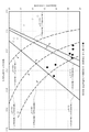
2 is a graph showing the relationship between the carrier concentration and the carrier mobility.
3 is a graph showing the relationship between carrier mobility / carrier concentration and light absorption.
4 is a graph showing the relationship between the light absorptivity of the ITO film in the absence of the light scattering layer and the light absorptivity of the ITO film in the presence of the light scattering layer.
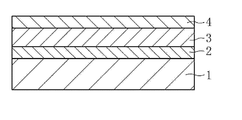
5 is a cross-sectional view showing an example of organic EL illumination.
이하, 본 발명의 일실시형태에 따른 투명 도전막을 갖는 기판이 조립된 유기 EL 조명을 설명한다.Hereinafter, an organic EL illumination in which a substrate having a transparent conductive film according to an embodiment of the present invention is assembled will be described.
본 발명의 일실시형태에 따른 투명 도전막을 갖는 기판이 조립된 유기 EL 조명은 예를 들면, 기판으로서의 유리 기판, 광 산란층, 평활층, 제 1 전극으로서의 투명 도전막, 유기 EL 발광층 및 제 2 전극으로서의 금속막을 순차적으로 구비하고 있다. 이 중, 이 실시형태에 따른 투명 도전막을 갖는 기판은 유리 기판, 광 산란층, 평활층 및 투명 도전막이다.The organic EL illuminator in which the substrate having the transparent conductive film according to the embodiment of the present invention is assembled includes, for example, a glass substrate as a substrate, a light scattering layer, a smoothing layer, a transparent conductive film as a first electrode, And a metal film as an electrode sequentially. Among them, the substrate having the transparent conductive film according to this embodiment is a glass substrate, a light scattering layer, a smoothing layer, and a transparent conductive film.
유리 기판으로서는 소다 유리, 무알칼리 유리 등이 사용된다. 유리 기판은 오버플로우 다운드로우법이나 플로트법 등에 의해 형성된다. 유리 기판의 두께는 예를 들면 0.3∼2mm이다. 유리 기판의 굴절률은 예를 들면 1.5∼1.7이다.As the glass substrate, soda glass, alkali-free glass, or the like is used. The glass substrate is formed by an overflow down-draw method, a float method, or the like. The thickness of the glass substrate is, for example, 0.3 to 2 mm. The refractive index of the glass substrate is, for example, 1.5 to 1.7.
광 산란층은 예를 들면, 유리 기판의 표면에 형성된 요철 구조로 이루어진다. 요철 구조로 이루어지는 광 산란층은 예를 들면, 유리 페이스트를 유리 기판의 표면에 스크린 인쇄함으로써 형성된다. 광 산란층의 두께는 예를 들면, 1∼10㎛이다. 광 산란층의 굴절률은 예를 들면, 1.4∼1.7이지만, 본 실시형태에서는 유리 기판의 굴절률과 정합되어 있다. 또한, 광 산란층은 광을 산란하는 기능을 갖는 것이면 특별하게 한정되는 것은 아니고, 예를 들면 평활한 층 중에 광 산란성을 갖는 물질(예를 들면, TiO2 등)을 분산시킨 구조 등이어도 된다.The light scattering layer is made of, for example, a concavo-convex structure formed on the surface of the glass substrate. The light scattering layer made of the concavo-convex structure is formed, for example, by screen printing a glass paste on the surface of a glass substrate. The thickness of the light scattering layer is, for example, 1 to 10 mu m. The refractive index of the light scattering layer is, for example, 1.4 to 1.7, but is matched with the refractive index of the glass substrate in the present embodiment. The light scattering layer is not particularly limited as long as it has a function of scattering light. For example, the light scattering layer may be a structure in which light scattering material (for example, TiO 2 ) is dispersed in a smooth layer.
평활층은 요철 구조로 이루어지는 광 산란층의 표면을 평활하게 고르게 하는 역할을 한다. 평활층은 예를 들면, 유리 페이스트를 광 산란층 상에 도포함으로써 형성된다. 평활층의 두께는 예를 들면 5∼50㎛이다. 평활층의 굴절률은 예를 들면 1.7∼2.1이지만, 이 실시형태에서는 투명 도전막의 굴절률과 정합되어 있다. 또한, 광 산란층이 평활한 층인 경우, 평활층은 생략해도 좋다.The smoothing layer serves to smoothen the surface of the light scattering layer made of the concave-convex structure. The smoothing layer is formed, for example, by applying a glass paste onto the light scattering layer. The thickness of the smoothing layer is, for example, 5 to 50 占 퐉. The refractive index of the smoothing layer is, for example, 1.7 to 2.1, but in this embodiment, it is matched with the refractive index of the transparent conductive film. When the light scattering layer is a smooth layer, the smoothing layer may be omitted.
투명 도전막은 ITO막으로 구성된다. 투명 도전막은 진공 증착법, 스퍼터링법 등에 의해 형성된다. 투명 도전막의 두께는 예를 들면, 20∼350nm이다. 투명 도전막의 굴절률은 예를 들면, 1.7∼2.1이다. 본 실시형태에서는 투명 도전막의 굴절률이 유리 기판의 굴절률보다 크다.The transparent conductive film is composed of an ITO film. The transparent conductive film is formed by a vacuum deposition method, a sputtering method, or the like. The thickness of the transparent conductive film is, for example, 20 to 350 nm. The refractive index of the transparent conductive film is, for example, 1.7 to 2.1. In the present embodiment, the refractive index of the transparent conductive film is larger than the refractive index of the glass substrate.
유기 EL 발광층은 단층 또는 다층 구조이다. 유기 EL 발광층은 진공 증착법, 스핀코트법, 캐스트법 등에 의해 형성된다. 유기 EL 발광층의 두께는 예를 들면 20∼200nm이다.The organic EL light emitting layer is a single layer or a multilayer structure. The organic EL light emitting layer is formed by a vacuum evaporation method, a spin coating method, a casting method, or the like. The thickness of the organic EL light-emitting layer is, for example, 20 to 200 nm.
금속막은 Al막 등으로 구성된다. 금속막은 진공 증착법, 스퍼터링법 등에 의해 형성된다. 금속막의 두께는 예를 들면, 50∼200nm이다.The metal film is made of an Al film or the like. The metal film is formed by a vacuum deposition method, a sputtering method, or the like. The thickness of the metal film is, for example, 50 to 200 nm.
이상과 같은 구성에 의해, 투명 도전막과 금속막에 의해, 유기 EL 발광층에 전압을 인가해서 유기 EL 발광층을 발광시키고, 그 발광시킨 광을 투명 도전막을 통과시키면서 광 산란층에 산란시킨다. 이것에 의해 유리 기판측으로부터 광을 인출하고, 소정의 대상물 등을 비춘다.With the above-described structure, a voltage is applied to the organic EL light-emitting layer by the transparent conductive film and the metal film to cause the organic EL light-emitting layer to emit light, and the emitted light is scattered in the light-scattering layer while passing through the transparent conductive film. Thereby, light is extracted from the glass substrate side, and a predetermined object or the like is illuminated.
그리고, 이렇게 광 산란층을 구비한 유기 EL 조명의 경우, 유기 EL 발광층에서 발광한 광은 광 산란층에서 산란해서 사방으로 확산하기 때문에, 광 산란층과 금속막 사이에서 반사를 반복하는 광의 성분이 많아진다. 그 결과, 광 산란층과 금속막 사이에 있는 투명 도전막에 있어서의 광의 흡수가 유기 EL 조명의 특성에 크게 영향을 준다.In the case of the organic EL illumination including the light scattering layer, the light emitted from the organic EL light emitting layer is scattered in the light scattering layer and diffuses in all directions. Therefore, a light component repeatedly reflected between the light scattering layer and the metal film More. As a result, the absorption of light in the transparent conductive film between the light scattering layer and the metal film greatly affects the characteristics of the organic EL illumination.
그래서, 투명 도전막은 다음과 같은 특성을 갖는 것으로 했다.Thus, the transparent conductive film has the following characteristics.
즉, 투명 도전막은 (캐리어 이동도)/(캐리어 농도)가 2×10-20cm5/V/S 이상이다. (캐리어 이동도)/(캐리어 농도)는 바람직하게는 3.2×10⁻²⁰cm 5/V/S 이상이고, 더욱 바람직하게는 3.6×10⁻²⁰cm5/V/S 이상이다. (캐리어 이동도)/(캐리어 농도)가 커지면, 투명 도전막의 광 흡수율이 작아진다. 그리고, (캐리어 이동도)/(캐리어 농도)가 2×10-20cm5/V/S 이상이 되면, 광 산란층을 갖는 유기 EL 조명에 사용해도 문제없는 정도까지, 투명 도전막(4)의 광 흡수율이 작아진다.That is, the transparent conductive film has a (carrier mobility) / (carrier concentration) of 2 x 10 -20 cm 5 / V / S or more. (Carrier mobility) / (carrier concentration) is preferably not less than 3.2 x 10 -20
또한, 투명 도전막은 (캐리어 이동도)×(캐리어 농도)가 200×1020cm-1/V/S 이상이다. (캐리어 이동도)×(캐리어 농도)는 바람직하게는 350×1020cm-1/V/S 이상이다. 또한, (캐리어 이동도)×(캐리어 농도)는 바람직하게는 505×1020cm-1/V/S 이하이다. (캐리어 이동도)×(캐리어 농도)가 커지면, 투명 도전막의 저항률이 작아진다. 그리고, (캐리어 이동도)×(캐리어 농도)가 200×1020cm-1/V/S 이상이 되면, 광 산란층을 갖는 유기 EL 조명에 사용해도 문제없는 정도까지, 투명 도전막의 저항률이 작아진다.The transparent conductive film has a (carrier mobility) x (carrier concentration) of 200 x 10 20 cm -1 / V / S or more. (Carrier mobility) x (carrier concentration) is preferably 350 x 10 20 cm -1 / V / s or more. The (carrier mobility) x (carrier concentration) is preferably 505 x 10 20 cm -1 / V / S or less. (Carrier mobility) x (carrier concentration) becomes large, the resistivity of the transparent conductive film becomes small. When the (carrier mobility) x (carrier concentration) is 200 x 10 20 cm -1 / V / S or more, the resistivity of the transparent conductive film is small to the extent that it can be used in organic EL lighting having a light scattering layer Loses.
여기서, 투명 도전막은 (캐리어 이동도)/(캐리어 농도)가 3.6×10⁻²⁰cm5/V/S이상이며, 또한 (캐리어 이동도)×(캐리어 농도)가 200×1020cm-1/V/S 이상인 것이 바람직하다. 또한, 투명 도전막은 (캐리어 이동도)/(캐리어 농도)가 2×10-20cm 5/V/S 이상, 505×10-20cm5/V/S 이하이고, 또한 (캐리어 이동도)×(캐리어 농도)가 200×1020cm-1/V/S 이상이어도 된다.Here, the transparent conductive film has a (carrier mobility) / (carrier concentration) of 3.6 x 10 -20 cm 5 / V / S or more and a (carrier mobility) x (carrier concentration) of 200 x 10 20 cm -1 / V / S or higher. The transparent conductive film has a (carrier mobility) / (carrier concentration) of 2 x 10 -20 cm 5 / V / S or more and 505 x 10 -20 cm 5 / V / (Carrier concentration) may be 200 x 10 20 cm -1 / V / S or more.
다음에, 상기 구성의 투명 도전막을 갖는 기판이 조립된 유기 EL 조명의 제조 방법의 일례를 설명한다. 또한, 이 제조 방법 중에서, 투명 도전막을 갖는 기판의 제조 방법도 아울러 설명한다.Next, an example of a method for manufacturing an organic EL illumination in which a substrate having the transparent conductive film having the above structure is assembled will be described. Among these manufacturing methods, a manufacturing method of a substrate having a transparent conductive film is also described.
(산란층의 형성 공정)(Scattering layer forming step)
우선, 유리 기판으로서, 소다 유리 기판을 준비한다. 다음에 유리 기판 상에 아연 붕산계 유리 페이스트를 스크린 인쇄함과 아울러, 대기 분위기 하에서 건조한다. 그 후, 대기 분위기 하에서 유리 페이스트를 소성함으로써, 유리 기판 상에 유리로 이루어지는 광 산란층을 형성한다. 또한, 유리 기판 및 광 산란층의 굴절률은 1.6으로 한다.First, a soda glass substrate is prepared as a glass substrate. Next, a zinc borate-based glass paste is screen-printed on a glass substrate and dried in an air atmosphere. Thereafter, the glass paste is baked in the air atmosphere to form a light scattering layer made of glass on the glass substrate. The refractive index of the glass substrate and the light scattering layer is 1.6.
(평활층의 형성 공정)(Smooth layer forming step)
이어서, 광 산란층 상에 비스무트계 유리 페이스트를 어플리케이터로 도포하고, 대기 분위기 하에 건조한다. 그 후, 대기 분위기 하에 유리 페이스트를 소성함으로써, 광 산란층 상에 유리로 이루어지는 평활층을 형성한다. 또한, 평활층의 굴절률은 1.9로 한다.Then, a bismuth-based glass paste is coated on the light scattering layer with an applicator, and dried in an air atmosphere. Thereafter, the glass paste is fired in an air atmosphere to form a smoothing layer made of glass on the light scattering layer. The refractive index of the smoothing layer is 1.9.
(투명 도전막의 형성 공정)(Step of forming transparent conductive film)
그 후, 평활층 상에 ITO막으로 이루어지는 투명 도전막을 스퍼터링법에 의해 형성한다. 스퍼터링 시에는 스퍼터링 장치의 챔버 내에 광 산란층 및 평활층이 형성된 유리 기판과 산화 인듐 주석의 타겟(성막 재료)을 배치한다. 이 상태에서, 챔버 내에 반응 가스로서 아르곤과 산소의 혼합 가스를 공급한다. 스퍼터링 시의 유리 기판의 온도는 150℃∼350℃로 한다.Thereafter, a transparent conductive film made of an ITO film is formed on the smoothing layer by a sputtering method. At the time of sputtering, a glass substrate on which a light scattering layer and a smoothing layer are formed and an indium tin oxide target (film forming material) are arranged in a chamber of a sputtering apparatus. In this state, a mixed gas of argon and oxygen is supplied as a reaction gas into the chamber. The temperature of the glass substrate at the time of sputtering is set at 150 캜 to 350 캜.
이 때, 챔버 내의 산소 농도는 0.5%∼0.9%, 바람직하게는 0.6%∼0.8%로 한다. 여기서, 도 1에 나타내는 바와 같이, 챔버 내의 산소 농도가 낮은 경우와 높은 경우에서, 투명 도전막(4)의 시트 저항 곡선의 기울기가 커지는 경향이 있다. 즉, 약간의 산소 농도 변화에 대하여 시트 저항이 크게 변화될 경향이 있다. 한편, 챔버 내의 산소 농도가 이들의 중간의 경우(0.2%∼0.5%)에서 투명 도전막(4)의 시트 저항 곡선의 기울기가 작아진다. 즉, 약간의 산소 농도 변화에 대하여 시트 저항 변화가 거의 보이지 않는다. 따라서, 통상, 투명 도전막은 시트 저항의 불균일을 작게 하기 위해서, 0.2%∼0.5%의 산소 농도의 범위에서 형성된다. 이에 대하여 본 실시형태에서는 챔버 내의 산소 농도가 높아지면, 제조되는 투명 도전막의 광 흡수율이 낮아진다고하는 지견에 의거하여 챔버 내의 산소 농도를 0.5% 이상으로 높게 설정하고 있다. 또한, 챔버 내의 산소 농도를 지나치게 높게 하면, 상술한 바와 같이, 투명 도전막의 시트 저항의 불균일이 지나치게 커지므로, 챔버 내의 산소 농도는 0.9% 이하로 하고 있다.At this time, the oxygen concentration in the chamber is 0.5% to 0.9%, preferably 0.6% to 0.8%. Here, as shown in Fig. 1, the inclination of the sheet resistance curve of the transparent
이상과 같은 조건에서 스퍼터링을 행함으로써 (캐리어 이동도)/(캐리어 농도)가 3.6×10⁻²⁰cm5/V/S 이상이고, 또한 (캐리어 이동도)×(캐리어 농도)가 200×1020cm-1/V/S 이상인 투명 도전막을 형성한다.(Carrier mobility) / (carrier concentration) is 3.6 x 10 -20 cm 5 / V / S or more and (carrier mobility) x (carrier concentration) is 200 x 10 20 cm < -1 > / V / S.
또한, 투명 도전막의 굴절률은 1.9로 한다.The refractive index of the transparent conductive film is 1.9.
(유기 EL 발광층의 형성 공정 및 금속막의 형성 공정)(A step of forming an organic EL light emitting layer and a step of forming a metal film)
다음에 투명 도전막 상에 유기 EL 발광층을 진공 증착법에 의해 형성한다. 그 후, 제 유기 EL 발광층 상에 금속막을 진공 증착법에 의해 형성한다.Next, an organic EL light emitting layer is formed on the transparent conductive film by a vacuum evaporation method. Thereafter, a metal film is formed on the organic EL light emitting layer by a vacuum evaporation method.
실시예Example
본 발명의 실시예 1∼8로서, 유리 기판 상에 ITO막을 스퍼터링법에 의해 형성하고, ITO막을 갖는 기판을 제조했다. 스퍼터링 시의 유리 기판의 온도는 350℃로 하고 챔버 내의 산소 농도는 0.5%∼0.9%의 범위 내에서 적당하게 조정했다.As Examples 1 to 8 of the present invention, an ITO film was formed on a glass substrate by a sputtering method to produce a substrate having an ITO film. The temperature of the glass substrate at the time of sputtering was set at 350 DEG C and the oxygen concentration in the chamber was appropriately adjusted within the range of 0.5% to 0.9%.
또한, 비교예 1은 챔버 내의 산소 농도 이외는 실시예 1∼8과 실질적으로 동일한 제조 조건이다.In addition, Comparative Example 1 is a manufacturing condition substantially the same as Examples 1 to 8 except for the oxygen concentration in the chamber.
이상과 같이 제조된 실시예 1∼8 및 비교예 1의 각종 특성을 평가한 결과를, 표 1에 나타낸다. 또한, 표 1에는 특허문헌 1 및 특허문헌 2의 대응하는 데이터를 비교예 2∼11로서 기재하고 있다. 비교예 9∼11의 저항률은 캐리어 농도와 캐리어 이동도의 값으로부터 연산에 의해 구하고 있다.Table 1 shows the results of evaluating various characteristics of Examples 1 to 8 and Comparative Example 1 manufactured as described above. In Table 1, corresponding data of
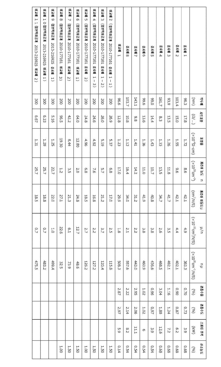
표 중의 실시예 1∼8 및 비교예 1에 있어서의 막두께는 Veeco사 제작의 Dektak 6M, 시트 저항은 Mitsubishi Chemical Analytech Co., Ltd. 제작 MCP-T360, 저항률, 캐리어 농도(n) 및 캐리어 이동도(μ)는 TOYO Corporation 제작의 ResiTest 8320을 이용하여 측정했다.The film thicknesses in Examples 1 to 8 and Comparative Example 1 in the Tables were Dektak 6M manufactured by Veeco Co., Ltd., sheet resistance was measured by Mitsubishi Chemical Analytech Co., Ltd. The prepared MCP-T360, resistivity, carrier concentration (n) and carrier mobility (μ) were measured using ResiTest 8320 manufactured by TOYO Corporation.
표 중의 실시예 1∼8 및 비교예 1에 있어서의 ITO막의 광 흡수율의 측정은 다음과 같이 하여 행했다. 또한, 하기의 1∼2, 4∼5에 있어서의 시감 투과율 및 시감 반사율은 Hitachi, Ltd. 제작의 U-4100 또는 Shimadzu Corporation 제작의 UV-3100PC를 이용하여 측정했다.The light absorptivity of the ITO films in Examples 1 to 8 and Comparative Example 1 in the tables was measured as follows. The luminous transmittance and luminous reflectance in the following
1. ITO막을 갖는 기판의 시감 투과율(A)을 ISO9050에 준거한 방법으로 측정한다.[측정 파장: 380nm∼780nm, 표준 광원: D65]1. A luminous transmittance (A) of a substrate having an ITO film is measured by a method in accordance with ISO 9050. [Measurement wavelength: 380 nm to 780 nm, standard light source: D65]
2. ITO막을 갖는 기판의 시감 반사율(B)을 ISO9050에 준거한 방법으로 측정한다.[측정 파장: 380nm∼780nm, 표준 광원: D65]2. The luminous reflectance (B) of the substrate having the ITO film was measured by a method in accordance with ISO 9050. [Measurement wavelength: 380 nm to 780 nm, standard light source: D65]
3. ITO막을 갖는 기판의 광 흡수율(C)=100%-(A)-(B)3. Light absorptivity (C) of a substrate having an ITO film = 100% - (A) - (B)
4. ITO막을 갖지 않는 기판의 시감 투과율(D)을 ISO9050에 준거한 방법으로 측정한다.[측정 파장: 380nm∼780nm, 표준 광원: D65]4. The luminous transmittance (D) of a substrate having no ITO film is measured by a method in accordance with ISO 9050. [Measurement wavelength: 380 nm to 780 nm, standard light source: D65]
5. ITO막을 갖지 않는 기판의 시감 반사율(E)을 ISO9050에 준거한 방법으로 측정한다.[측정 파장: 380nm∼780nm, 표준 광원: D65]5. The luminous reflectance (E) of the substrate having no ITO film is measured by a method in accordance with ISO 9050. [Measurement wavelength: 380 nm to 780 nm, standard light source: D65]
6. ITO막을 갖지 않는 기판의 광 흡수율(F)=100%-(D)-(E)6. Light absorptivity (F) of the substrate having no ITO film = 100% - (D) - (E)
7. ITO막의 광 흡수율(G)=(C)-(F)7. Light absorption rate (G) of the ITO film = (C) - (F)
표 중의 실시예 1∼8 및 비교예 1에 있어서의 광 흡수율은 막두께에 의존한다. 즉, 막두께가 커지면, 광 흡수율은 필연적으로 높아진다. 그 때문에 광 흡수율의 값을 100nm의 막두께당의 값으로 규격화한 것을 광 흡수도로 했다.The light absorptivity in Examples 1 to 8 and Comparative Example 1 in the tables depends on the film thickness. That is, as the film thickness increases, the light absorption rate necessarily increases. For this reason, the value of the light absorption rate was normalized to a value per 100 nm of film thickness, and the light absorption was obtained.
다음에, 표 1에 나타낸 실시예 1∼8 및 비교예 1∼11에 있어서의 캐리어 농도와 캐리어 이동도의 관계를 도 2에 나타낸다.Next, the relationship between carrier concentration and carrier mobility in Examples 1 to 8 and Comparative Examples 1 to 11 shown in Table 1 is shown in Fig.
도 2로부터, (캐리어 이동도)/(캐리어 농도)가 2×10-20cm 5/V/S 이상이고, 또한, (캐리어 이동도)×(캐리어 농도)가 200×1020cm-1/V/S 이상인 범위 내에 실시예 1∼8이 있고, 비교예 1∼11은 이 범위 외에 있는 것을 확인할 수 있다. 그리고, 표 1로부터 실시예 1∼8은 저항률이 1.72×10⁻⁴(Ω·cm) 이하이고, 또한 광 흡수도가 2.14% 이하인 것이 확인된다. 이에 대하여 비교예 1은 저항률이 1.23×10⁻⁴(Ω·cm)이고, 또한 광 흡수도가 2.97%이다. 즉, 비교예 1에서는 저항률은 낮지만, 광 흡수도가 높게 되어 있지만, 실시예 1∼8에서는 저항률과 광 흡수도가 함께 낮아진다고 하는 양호한 결과로 되어 있다. 또한, 유기 EL 조명의 경우, 저항률보다 광 흡수도쪽이 특성에 주는 영향이 크다고 생각된다.2 shows that (carrier mobility) / (carrier concentration) is 2 x 10 -20
또한, 표 1에 나타낸 실시예 1∼8에 있어서의 (캐리어 이동도)/(캐리어 농도)와 광 흡수도의 관계를 도 3에 나타낸다.Fig. 3 shows the relationship between (carrier mobility) / (carrier concentration) and light absorption in Examples 1 to 8 shown in Table 1.
도 3으로부터, (캐리어 이동도)/(캐리어 농도)가 커짐에 따라서 광 흡수도가 작아지는 것을 인식할 수 있다. 즉, (캐리어 이동도)/(캐리어 농도)가 광 흡수도를 평가하는 파라미터로서 유효한 것을 인식할 수 있다.It can be seen from Fig. 3 that as the (carrier mobility) / (carrier concentration) increases, the light absorption becomes smaller. That is, it can be recognized that (carrier mobility) / (carrier concentration) is effective as a parameter for evaluating light absorption.
여기서, 광 산란층이 없는 경우에 있어서의 ITO막의 광 흡수율(가로축)과 광 산란층이 있는 경우의 ITO막의 광 흡수율(세로축)의 관계를 도 4에 나타낸다.4 shows the relationship between the light absorptance (horizontal axis) of the ITO film in the absence of the light scattering layer and the light absorption rate (vertical axis) of the ITO film in the presence of the light scattering layer.
도 4에서, 유리 기판과 ITO막으로 이루어지는 투명 도전막을 갖는 기판(광 산란층 없음)에 있어서 ITO막의 광 흡수율이 낮아지면, 유리 기판과 광 산란층과 ITO막으로 이루어지는 투명 도전막을 갖는 기판(광 산란층 있음)에 있어서도 ITO막의 광 흡수율이 낮아지는 것을 인식할 수 있다. 따라서, 유리 기판과 ITO막으로 이루어지는 투명 도전막을 갖는 기판을 사용한 상술의 평가 시험에 의해 얻어진 결과는 광 산란층을 형성한 경우에도 마찬가지로 적용된다. 즉, ITO막의 (캐리어 이동도)/(캐리어 농도)가 2×10-20cm5/V/S 이상이고, 또한 (캐리어 이동도)×(캐리어 농도)가 200×1020cm-1/V/S 이상인 범위 내이면, 광 산란층을 갖는 투명 도전막을 갖는 기판의 경우에도, ITO막의 저항률과 광 흡수율(또는 광 흡수도)가 함께 작아지는 것은 명확하다.4, when the light absorptivity of the ITO film in the substrate (without the light scattering layer) having the transparent conductive film made of the glass substrate and the ITO film is lowered, the substrate having the transparent conductive film made of the glass substrate, the light scattering layer and the ITO film It is possible to recognize that the light absorptivity of the ITO film is also lowered even in the case of using a scattering layer. Therefore, the result obtained by the above-described evaluation test using the substrate having the transparent conductive film made of the glass substrate and the ITO film is similarly applied even when the light scattering layer is formed. (Carrier mobility) / (carrier concentration) of the ITO film is 2 x 10 -20 cm 5 / V / S or more and (carrier mobility) x (carrier concentration) is 200 x 10 20 cm -1 / V / S, it is clear that the resistivity of the ITO film and the light absorption rate (or the light absorption degree) are also reduced in the case of the substrate having the transparent conductive film having the light scattering layer.
이상, 본 발명의 일실시형태를 설명했지만, 상술한 유기 EL 조명 및 그 제조 방법은 당연하게 본 발명의 범위 내에 있어서 임의의 형태를 채용할 수 있다.As described above, one embodiment of the present invention has been described. However, the above-described organic EL illumination and the manufacturing method thereof can naturally take any form within the scope of the present invention.
예를 들면, 상술의 실시형태에서는 광 산란층을 갖는 유기 EL 조명에 본 발명을 적용한 경우를 설명했지만, 광 산란층을 갖지 않는 유기 EL 조명에 본 발명에 따른 투명 도전막 및 투명 도전막을 갖는 기판을 적용해도 좋다. 즉, 도 5에 나타내는 바와 같이, 유기 EL 조명은 유리 기판(1), 투명 도전막(2), 유기 EL 발광층(3) 및 금속막(4)으로 구성되어 있어도 된다. 이 경우, 투명 도전막을 갖는 기판은 유리 기판(1)과 투명 도전막(2)으로 구성된다.For example, in the above-described embodiments, the case where the present invention is applied to the organic EL illumination having the light scattering layer has been described. However, in the organic EL illumination without the light scattering layer, the transparent conductive film according to the present invention and the substrate May be applied. 5, the organic EL illumination may be composed of the
또한, 상술의 실시형태에서는 본 발명을 유기 EL 조명에 적용하는 경우를 설명했지만, 본 발명에 따른 투명 도전막 및 투명 도전막을 갖는 기판을 디스플레이장치 등에 적용해도 좋다.In the above-described embodiments, the case where the present invention is applied to the organic EL illumination has been described. However, the transparent conductive film and the substrate having the transparent conductive film according to the present invention may be applied to a display device or the like.
1 : 유리 기판 2 : 투명 도전막(제 1 전극)
3 : 유기 EL 발광층 4 : 금속막(제 2 전극)1: glass substrate 2: transparent conductive film (first electrode)
3: organic EL light emitting layer 4: metal film (second electrode)
Claims (4)
(캐리어 이동도)/(캐리어 농도)가 2×10-20cm5/V/S 이상이고, 또한 (캐리어 이동도)×(캐리어 농도)가 200×1020cm-1/V/S 이상인 것을 특징으로 하는 투명 도전막.A transparent conductive film comprising an indium tin oxide film,
(Carrier mobility) / (carrier concentration) of 2 x 10 -20 cm 5 / V / S or more and (carrier mobility) x (carrier concentration) of 200 x 10 20 cm -1 / V / A transparent conductive film characterized by:
(캐리어 이동도)/(캐리어 농도)가 3.6×10⁻²⁰cm5/V/S 이상인 것을 특징으로 하는 투명 도전막.The method according to claim 1,
(Carrier mobility) / (carrier concentration) of 3.6 × 10 -20 cm 5 / V / S or higher.
상기 투명 도전막의 캐리어 이동도를 μ(cm2/V/S), 캐리어 농도를 n(cm-3)으로 한 경우에,
μ/n이 2×10-20cm5/V/S 이상이고, 또한 μ×n이 200×1020cm-1/V/S 이상인 것을 특징으로 하는 투명 도전막을 갖는 기판.A substrate having a transparent conductive film having a transparent conductive film composed of a light scattering layer and an indium tin oxide film on a substrate,
When the carrier mobility of the transparent conductive film is μ (cm 2 / V / S) and the carrier concentration is n (cm -3 )
a substrate having a transparent conductive film, wherein a ratio mu / n is not less than 2 x 10 < -20 cm < 5 / V / S and a x x n is not less than 200 x 10 20 cm- 1 / V /
상기 기판을 산화 인듐 주석의 타겟을 갖는 챔버 내에 배치함과 아울러, 상기 챔버 내의 산소 농도를 0.5%∼0.9%로 한 상태에서 스퍼터링을 행하는 것을 특징으로 하는 투명 도전막을 갖는 기판의 제조 방법.
A method of manufacturing a substrate having a transparent conductive film having a transparent conductive film made of an indium tin oxide film on a substrate,
Wherein the substrate is placed in a chamber having a target of indium tin oxide and the sputtering is carried out with the oxygen concentration in the chamber being 0.5% to 0.9%.
Applications Claiming Priority (3)
| Application Number | Priority Date | Filing Date | Title |
|---|---|---|---|
| JPJP-P-2015-251989 | 2015-12-24 | ||
| JP2015251989A JP2017115206A (en) | 2015-12-24 | 2015-12-24 | Transparent conductive film, transparent conductive film-attached substrate, and production method of transparent conductive film-attached substrate |
| PCT/JP2016/086897 WO2017110551A1 (en) | 2015-12-24 | 2016-12-12 | Transparent conductive film, substrate provided with transparent conductive film, and method for producing substrate provided with transparent conductive film |
Publications (1)
| Publication Number | Publication Date |
|---|---|
| KR20180098216A true KR20180098216A (en) | 2018-09-03 |
Family
ID=59090271
Family Applications (1)
| Application Number | Title | Priority Date | Filing Date |
|---|---|---|---|
| KR1020187007335A Withdrawn KR20180098216A (en) | 2015-12-24 | 2016-12-12 | A transparent conductive film, a substrate having a transparent conductive film, and a method of manufacturing a substrate having a transparent conductive film |
Country Status (6)
| Country | Link |
|---|---|
| US (1) | US20210193950A1 (en) |
| EP (1) | EP3396013A4 (en) |
| JP (1) | JP2017115206A (en) |
| KR (1) | KR20180098216A (en) |
| TW (1) | TW201738181A (en) |
| WO (1) | WO2017110551A1 (en) |
Families Citing this family (1)
| Publication number | Priority date | Publication date | Assignee | Title |
|---|---|---|---|---|
| CN113106405A (en) * | 2021-03-18 | 2021-07-13 | 上海交通大学 | Method for reducing infrared absorption rate of ITO film |
Citations (3)
| Publication number | Priority date | Publication date | Assignee | Title |
|---|---|---|---|---|
| JP2010177161A (en) | 2009-02-02 | 2010-08-12 | Toyobo Co Ltd | Transparent conductive film |
| JP2013518361A (en) | 2010-01-22 | 2013-05-20 | サン−ゴバン グラス フランス | Glass substrate coated with high refractive index layer under electrode coating and organic light emitting device comprising the substrate |
| JP2013216925A (en) | 2012-04-05 | 2013-10-24 | Toppan Printing Co Ltd | Method for producing transparent conductive film and transparent conductive substrate |
Family Cites Families (7)
| Publication number | Priority date | Publication date | Assignee | Title |
|---|---|---|---|---|
| JP3427648B2 (en) * | 1995-03-22 | 2003-07-22 | 凸版印刷株式会社 | Electrode plate and liquid crystal display device using the same |
| JPH09324264A (en) * | 1996-06-03 | 1997-12-16 | Toppan Printing Co Ltd | Sputtering target |
| JP3615647B2 (en) * | 1998-01-06 | 2005-02-02 | 株式会社神戸製鋼所 | Method for producing transparent conductive film and transparent conductive film |
| JP2000233969A (en) * | 1998-12-08 | 2000-08-29 | Tosoh Corp | Method for producing ITO sputtering target and transparent conductive film |
| JP4397511B2 (en) * | 1999-07-16 | 2010-01-13 | Hoya株式会社 | Low resistance ITO thin film and manufacturing method thereof |
| JP2002343151A (en) * | 2001-03-07 | 2002-11-29 | Ueyama Denki:Kk | Method for manufacturing transparent conductive film laminated substrate |
| JP2009004275A (en) * | 2007-06-22 | 2009-01-08 | Panasonic Electric Works Co Ltd | Surface light emitter and method of manufacturing surface light emitter |
-
2015
- 2015-12-24 JP JP2015251989A patent/JP2017115206A/en not_active Ceased
-
2016
- 2016-12-12 EP EP16878442.9A patent/EP3396013A4/en not_active Withdrawn
- 2016-12-12 WO PCT/JP2016/086897 patent/WO2017110551A1/en not_active Ceased
- 2016-12-12 US US16/065,184 patent/US20210193950A1/en not_active Abandoned
- 2016-12-12 KR KR1020187007335A patent/KR20180098216A/en not_active Withdrawn
- 2016-12-19 TW TW105142071A patent/TW201738181A/en unknown
Patent Citations (3)
| Publication number | Priority date | Publication date | Assignee | Title |
|---|---|---|---|---|
| JP2010177161A (en) | 2009-02-02 | 2010-08-12 | Toyobo Co Ltd | Transparent conductive film |
| JP2013518361A (en) | 2010-01-22 | 2013-05-20 | サン−ゴバン グラス フランス | Glass substrate coated with high refractive index layer under electrode coating and organic light emitting device comprising the substrate |
| JP2013216925A (en) | 2012-04-05 | 2013-10-24 | Toppan Printing Co Ltd | Method for producing transparent conductive film and transparent conductive substrate |
Also Published As
| Publication number | Publication date |
|---|---|
| WO2017110551A1 (en) | 2017-06-29 |
| TW201738181A (en) | 2017-11-01 |
| JP2017115206A (en) | 2017-06-29 |
| EP3396013A4 (en) | 2019-08-28 |
| EP3396013A1 (en) | 2018-10-31 |
| US20210193950A1 (en) | 2021-06-24 |
Similar Documents
| Publication | Publication Date | Title |
|---|---|---|
| TWI389597B (en) | Electroluminescent element and lighting device | |
| TWI494955B (en) | Conducting film or electrode with improved optical and electrical performance | |
| KR20100106412A (en) | Substrate carrying an electrode, organic electroluminescent device comprising said substrate, and production thereof | |
| JP2009004275A (en) | Surface light emitter and method of manufacturing surface light emitter | |
| TWI483270B (en) | Transparent conductivity film with excellent electric property and touch panel using the same | |
| JP2005063704A (en) | Organic EL device | |
| CN104321897B (en) | Organic Photonic Devices | |
| CN103190012A (en) | Support for organic-light-emitting-diode device, such an organic-light-emitting-diode device and process for manufacturing said device | |
| EP3200195A1 (en) | Flexible substrate and method of manufacturing same | |
| JP2023125926A (en) | Self-luminous display device | |
| CN105723540B (en) | Light-extraction substrate for organic light-emitting element, manufacturing method thereof, and organic light-emitting element including same | |
| US8067886B2 (en) | Composite optical destructive electrode for high contrast electroluminescent devices | |
| US20170358763A1 (en) | Flexible substrate and method of manufacturing same | |
| CN103490015B (en) | For light extraction substrate and its manufacture method of OLED | |
| TWI673898B (en) | Light extraction substrate for organic light-emitting diode, method of fabricating the same, and organic light-emitting diode device including the same | |
| WO2017110551A1 (en) | Transparent conductive film, substrate provided with transparent conductive film, and method for producing substrate provided with transparent conductive film | |
| KR101695525B1 (en) | Manufacturing method of metal oxide nanoparticle scattering film, organic light emitting diodes having the same | |
| RU2685086C2 (en) | Transparent supported electrode for oled | |
| JPH1148387A (en) | Transparent conductive film | |
| JP7184510B2 (en) | Light-transmitting conductive film for light control film and light control film | |
| CN109524569B (en) | Organic electroluminescent device and method of making the same, display panel and display device | |
| JP6637286B2 (en) | Light transmitting conductive film and light transmitting film with hard coat | |
| WO2019194010A1 (en) | Transparent conductor, method for manufacturing same, and organic device | |
| BE1019243A3 (en) | TRANSPARENT SUBSTRATE FOR PHOTONIC DEVICES. | |
| TW201935726A (en) | Light extraction device |
Legal Events
| Date | Code | Title | Description |
|---|---|---|---|
| PA0105 | International application |
Patent event date: 20180314 Patent event code: PA01051R01D Comment text: International Patent Application |
|
| PG1501 | Laying open of application | ||
| PC1203 | Withdrawal of no request for examination | ||
| WITN | Application deemed withdrawn, e.g. because no request for examination was filed or no examination fee was paid |