KR20180098125A - Tape for semiconductor processing - Google Patents
Tape for semiconductor processing Download PDFInfo
- Publication number
- KR20180098125A KR20180098125A KR1020177031446A KR20177031446A KR20180098125A KR 20180098125 A KR20180098125 A KR 20180098125A KR 1020177031446 A KR1020177031446 A KR 1020177031446A KR 20177031446 A KR20177031446 A KR 20177031446A KR 20180098125 A KR20180098125 A KR 20180098125A
- Authority
- KR
- South Korea
- Prior art keywords
- adhesive layer
- tape
- semiconductor
- metal layer
- resin
- Prior art date
- Legal status (The legal status is an assumption and is not a legal conclusion. Google has not performed a legal analysis and makes no representation as to the accuracy of the status listed.)
- Granted
Links
Images

Classifications
-
- C—CHEMISTRY; METALLURGY
- C09—DYES; PAINTS; POLISHES; NATURAL RESINS; ADHESIVES; COMPOSITIONS NOT OTHERWISE PROVIDED FOR; APPLICATIONS OF MATERIALS NOT OTHERWISE PROVIDED FOR
- C09J—ADHESIVES; NON-MECHANICAL ASPECTS OF ADHESIVE PROCESSES IN GENERAL; ADHESIVE PROCESSES NOT PROVIDED FOR ELSEWHERE; USE OF MATERIALS AS ADHESIVES
- C09J7/00—Adhesives in the form of films or foils
- C09J7/20—Adhesives in the form of films or foils characterised by their carriers
- C09J7/28—Metal sheet
-
- H01L23/36—
-
- H—ELECTRICITY
- H10—SEMICONDUCTOR DEVICES; ELECTRIC SOLID-STATE DEVICES NOT OTHERWISE PROVIDED FOR
- H10W—GENERIC PACKAGES, INTERCONNECTIONS, CONNECTORS OR OTHER CONSTRUCTIONAL DETAILS OF DEVICES COVERED BY CLASS H10
- H10W40/00—Arrangements for thermal protection or thermal control
- H10W40/10—Arrangements for heating
-
- C09J2201/622—
-
- C—CHEMISTRY; METALLURGY
- C09—DYES; PAINTS; POLISHES; NATURAL RESINS; ADHESIVES; COMPOSITIONS NOT OTHERWISE PROVIDED FOR; APPLICATIONS OF MATERIALS NOT OTHERWISE PROVIDED FOR
- C09J—ADHESIVES; NON-MECHANICAL ASPECTS OF ADHESIVE PROCESSES IN GENERAL; ADHESIVE PROCESSES NOT PROVIDED FOR ELSEWHERE; USE OF MATERIALS AS ADHESIVES
- C09J2203/00—Applications of adhesives in processes or use of adhesives in the form of films or foils
- C09J2203/326—Applications of adhesives in processes or use of adhesives in the form of films or foils for bonding electronic components such as wafers, chips or semiconductors
-
- C—CHEMISTRY; METALLURGY
- C09—DYES; PAINTS; POLISHES; NATURAL RESINS; ADHESIVES; COMPOSITIONS NOT OTHERWISE PROVIDED FOR; APPLICATIONS OF MATERIALS NOT OTHERWISE PROVIDED FOR
- C09J—ADHESIVES; NON-MECHANICAL ASPECTS OF ADHESIVE PROCESSES IN GENERAL; ADHESIVE PROCESSES NOT PROVIDED FOR ELSEWHERE; USE OF MATERIALS AS ADHESIVES
- C09J2301/00—Additional features of adhesives in the form of films or foils
- C09J2301/30—Additional features of adhesives in the form of films or foils characterized by the chemical, physicochemical or physical properties of the adhesive or the carrier
- C09J2301/312—Additional features of adhesives in the form of films or foils characterized by the chemical, physicochemical or physical properties of the adhesive or the carrier parameters being the characterizing feature
Landscapes
- Chemical & Material Sciences (AREA)
- Organic Chemistry (AREA)
- Adhesives Or Adhesive Processes (AREA)
- Dicing (AREA)
- Adhesive Tapes (AREA)
- Container, Conveyance, Adherence, Positioning, Of Wafer (AREA)
- Cooling Or The Like Of Semiconductors Or Solid State Devices (AREA)
- Engineering & Computer Science (AREA)
- Materials Engineering (AREA)
Abstract
반도체 웨이퍼에의 접합 시에 금속층에 주름이 발생하는 것을 방지할 수 있는 반도체 가공용 테이프를 제공한다. 본 발명의 반도체 가공용 테이프(10)는, 기재 필름(11)과 점착제층(12)을 갖는 다이싱 테이프(13)와, 상기 점착제층(12) 상에 설치되어 있고, 반도체 칩의 이면을 보호하기 위한 금속층(14)과, 상기 금속층(14) 상에 설치되어 있고, 상기 금속층(14)을 반도체 칩의 이면에 접착하기 위한 접착제층(15)을 갖고, 상기 다이싱 테이프(13)의 루프 스티프니스가 20mN 이상 200mN 미만인 것을 특징으로 한다.Provided is a tape for semiconductor processing that can prevent wrinkles from being generated in a metal layer at the time of bonding to a semiconductor wafer. A tape for semiconductor processing (10) of the present invention comprises a dicing tape (13) having a base film (11) and a pressure sensitive adhesive layer (12) And an adhesive layer (15) provided on the metal layer (14) for adhering the metal layer (14) to the back surface of the semiconductor chip, wherein the adhesive layer (15) And has a stiffness of 20 mN or more and less than 200 mN.
Description
본 발명은, 반도체 가공용 테이프에 관한 것으로, 특히 페이스 다운(face down) 방식으로 실장되는 반도체 칩의 이면을 보호하기 위한 금속층을 갖는 반도체 가공용 테이프에 관한 것이다.The present invention relates to a tape for semiconductor processing, and more particularly to a tape for semiconductor processing having a metal layer for protecting the back surface of a semiconductor chip mounted in a face down manner.
최근 들어, 반도체 장치 및 그 패키지의 박형화, 소형화가 보다 한층 요구되고 있다. 소위 페이스 다운(face down) 방식이라고 불리는 실장법을 사용한 반도체 장치의 제조가 행하여지고 있다. 페이스 다운 방식에서는, 회로면에 도통을 확보하기 위한 범프라고 불리는 볼록 형상의 전극이 형성되어 이루어지는 반도체 칩을 사용하여, 회로면을 반전(페이스 다운)시켜, 전극을 기판에 접속하는 구조(소위 플립 칩 접속)가 된다.In recent years, there is a further demand for thinning and miniaturization of semiconductor devices and their packages. A semiconductor device using a mounting method called a face down method has been produced. In the face down system, a semiconductor chip having a convex electrode called bump for securing conduction on the circuit surface is used to reverse the circuit surface (face down) and connect the electrode to the substrate Chip connection).
이러한 반도체 장치에서는, 반도체 칩의 이면을 반도체 가공용 테이프에 의해 보호하여, 반도체 칩의 손상 등을 방지하고 있는 경우가 있다(특허문헌 1 참조). 또한, 반도체 소자 상에, 금속층과 접착층을 포함하는 편면 접착 필름을, 접착층을 개재해서 부착하는 것도 알려져 있다(특허문헌 2 참조).In such a semiconductor device, the back surface of the semiconductor chip is protected by a semiconductor processing tape to prevent damage to the semiconductor chip (see Patent Document 1). It is also known to adhere a single-sided adhesive film containing a metal layer and an adhesive layer on a semiconductor element via an adhesive layer (see Patent Document 2).
플립 칩 접속의 대표적인 수순으로서는, 반도체 가공용 테이프를 접착한 반도체 칩 표면에 형성된 땜납 범프 등을 플럭스에 침지하고, 그 후 범프와 기판 상에 형성된 전극(필요에 따라 이 전극 상에도 땜납 범프가 형성되어 있음)을 접촉시키고, 마지막으로 땜납 범프를 용융시켜 땜납 범프와 전극을 리플로우 접속시킨다. 플럭스는, 납땜 시의 땜납 범프의 세정이나 산화의 방지, 땜납의 습윤성의 개선 등을 목적으로 사용되고 있다. 이상의 수순에 의해, 반도체 칩과 기판과의 사이의 양호한 전기적 접속을 구축할 수 있다.As a typical procedure of flip chip bonding, a solder bump or the like formed on the surface of a semiconductor chip to which a semiconductor processing tape is bonded is immersed in a flux, and then the bump and an electrode formed on the substrate (solder bumps are formed on the electrode as necessary And finally, the solder bumps are melted to reflowly connect the solder bumps and the electrodes. The flux is used for the purpose of cleaning the solder bumps during soldering, preventing oxidation, and improving the wettability of the solder. By the above procedure, it is possible to establish good electrical connection between the semiconductor chip and the substrate.
그래서, 플럭스가 부착되어도 얼룩의 발생을 방지할 수 있어, 외관성이 우수한 반도체 장치를 제조 가능한 반도체 가공용 테이프로서, 접착제층과, 이 접착제층 상에 적층된 보호층을 구비하고, 보호층을 유리 전이 온도가 200℃ 이상인 내열성 수지 또는 금속을 포함한 플립 칩형 반도체 이면용 필름이 제안되어 있다(특허문헌 3 참조).Thus, there is provided a semiconductor processing tape capable of manufacturing a semiconductor device having excellent appearance, which can prevent the occurrence of stains even when a flux is adhered, and has an adhesive layer and a protective layer laminated on the adhesive layer, A heat-resistant resin having a transition temperature of 200 DEG C or higher or a flip-chip type semiconductor backside film containing metal has been proposed (see Patent Document 3).
그러나, 상기 특허문헌 1과 같이, 방사선 경화성 성분 또는 열경화성 성분을 포함한 수지를 방사선 또는 열에 의해 경화시켜 보호막을 형성하는 경우, 경화 후의 보호막과 반도체 웨이퍼의 열팽창 계수 차가 크기 때문에, 가공 도중의 반도체 웨이퍼나 반도체 칩에 휨이 발생한다는 문제가 있었다.However, in the case of forming a protective film by curing a resin containing a radiation-curable component or a thermosetting component by radiation or heat as in the
이 점, 상기 특허문헌 2나 특허문헌 3과 같이, 금속의 보호층(이하, 금속층이라고 함)을 접착제층을 개재해서 반도체 웨이퍼에 접착함으로써 휨은 방지할 수 있다. 여기서, 특허문헌 3에는, 기재 상에 점착제층이 적층된 다이싱 테이프의 점착제층 상에, 보호층 및 접착제층을 형성한 플립 칩형 반도체 이면용 필름도 개시되어 있다.In this regard, as in the case of Patent Document 2 and Patent Document 3, warpage can be prevented by adhering a protective layer of metal (hereinafter referred to as a metal layer) to a semiconductor wafer via an adhesive layer. Patent Document 3 discloses a flip-chip type semiconductor backing film in which a protective layer and an adhesive layer are formed on a pressure-sensitive adhesive layer of a dicing tape having a pressure-sensitive adhesive layer laminated on a substrate.
이러한 다이싱 테이프 일체형의 플립 칩형 반도체 이면용 필름(이하, 반도체 가공용 테이프라고 함)은, 통상 접착제층 상에는 접착제층을 보호하기 위해서 세퍼레이터가 설치되어 있고, 반도체 웨이퍼에 접착제층을 접합할 때는, 접착제층에 주름이 생긴 상태에서 반도체 웨이퍼가 접합되어버리지 않도록, 접착제층측을 아래로 해서 세퍼레이터를 조금씩 박리하면서, 다이싱 테이프측으로부터 접합 롤러로 누르면서 접합한다. 이렇게 접합했을 때, 종래의 반도체 가공용 테이프에서는, 금속층에 주름이 발생한다는 문제가 있었다.A flip chip type semiconductor backing film (hereinafter referred to as a semiconductor processing tape) having a dicing tape integral type is usually provided with a separator on the adhesive layer in order to protect the adhesive layer. When bonding the adhesive layer to the semiconductor wafer, The separator is peeled little by little with the adhesive layer side down so that the semiconductor wafer is not bonded while the wrinkles are formed on the layer. When bonded in this manner, there is a problem that wrinkles are generated in the metal layer in the conventional semiconductor processing tape.
보호층의 주름은 이하의 메커니즘에 의해 발생한다고 추정된다. 세퍼레이터를 박리할 때 플립 칩형 반도체 이면용 필름에는 일 방향으로 장력이 가해진다. 다이싱 테이프는 익스팬드성을 갖기 때문에, 장력이 가해지는 방향으로 신장되어 변형되기 때문에, 장력이 가해지는 방향을 따라서 주름이 발생한다. 그렇게 하면, 다이싱 테이프 상에 설치된 금속층 및 접착제층에도 주름이 발생한다. 그러나, 플립 칩형 반도체 이면용 필름은, 세퍼레이터가 박리된 직후에 접합 롤러로 눌려지고, 이때, 다이싱 테이프와 접착제층은 유연성에 여유가 있기 때문에, 접합 롤러를 따른 방향으로 잡아 당겨져, 세퍼레이터의 박리 시에 발생한 주름이 해소된다. 그러나, 금속을 포함하는 보호층은 이것에 추종할 수 없어, 주름이 발생한 상태에서 접합되어버리는 것으로 생각된다.It is presumed that the corrugation of the protective layer is caused by the following mechanism. When the separator is peeled off, tensile force is applied to the flip chip type semiconductor backside film in one direction. Since the dicing tape has expandable property, the dicing tape is stretched and deformed in the direction in which the tension is applied, so that wrinkles occur along the direction in which the tension is applied. As a result, wrinkles also occur in the metal layer and the adhesive layer provided on the dicing tape. However, the flip chip type semiconductor backing film is pressed by the bonding roller immediately after the separator is peeled off. At this time, since the dicing tape and the adhesive layer have flexibility, they are pulled in the direction along the bonding roller, The wrinkles generated at the time are eliminated. However, it is considered that the protective layer containing a metal can not follow it, and the protective layer including the metal is bonded in a state where wrinkles are generated.
상술한 바와 같이 반도체 가공용 테이프는, 통상 긴 세퍼레이터 상에 반도체 웨이퍼에 대응하는 소정 형상으로 프리컷된 보호층 및 접착제층이 형성된 플립 칩형 반도체 이면용 필름과 다이싱 테이프를 보호층과 점착제층이 합쳐지도록 접합해서, 다이싱 테이프를 기재 필름측으로부터 링 프레임에 대응하는 소정 형상(통상은 원형)으로 프리컷 가공한 것이 롤 형상으로 감긴 형상으로 되어 있다. 이렇게 롤 형상의 반도체 가공용 테이프를 사용한 경우에, 특히 금속층의 주름의 발생은 현저하다. 이하에, 도 3을 사용해서 보다 상세하게 설명한다.As described above, the semiconductor processing tape generally comprises a flip-chip type semiconductor backside film on which a protective layer and an adhesive layer are precut and formed in a predetermined shape corresponding to a semiconductor wafer on a long separator, and a dicing tape is combined with a protective layer and a pressure- And the dicing tape is pre-cut from a base film side to a predetermined shape (usually circular) corresponding to the ring frame, and is formed into a roll-like shape. When a roll-shaped semiconductor processing tape is used in this manner, the generation of wrinkles in the metal layer is remarkable. Hereinafter, this will be described in more detail with reference to FIG.
먼저, 반도체 가공용 테이프(100)를 반도체 웨이퍼(W) 및 링 프레임(R)에 접합하는 장치·방법을 개략적으로 설명한다. 롤 형상으로 감긴 반도체 가공용 테이프(100)는, 도 3에서 A 방향으로 시트 형상으로 인출되어, B 방향으로 권취 롤러(102)에 의해 권취되어 간다. 반도체 가공용 테이프(100)의 인출 경로에는, 박리용 쐐기(103)가 설치되어 있고, 박리용 쐐기(103)의 선단부를 되꺾는 점으로 해서, 세퍼레이터(101)만이 박리되어, 권취 롤러(102)에 권취된다. 박리용 쐐기(103)의 선단부의 하방에는, 접합 대(104)가 설치되어 있고, 접합 대(104)의 상면에는, 반도체 웨이퍼(W) 및 링 프레임(R)이 배치되어 있다. 박리용 쐐기(103)에 의해 세퍼레이터(101)로부터 박리된 플립 칩형 반도체 이면용 필름(105)(금속층과 접착제층의 적층체) 및 다이싱 테이프(106)는, 링 프레임(R) 및 반도체 웨이퍼(W) 상에 유도되어, 접합 롤러(107)에 의해 링 프레임(R) 및 반도체 웨이퍼(W)에 접합된다. 접합 대(104)는, 도 3에서 좌측 방향으로 이동하고 있고, 다음의 링 프레임(R) 및 반도체 웨이퍼(W)에 플립 칩형 반도체 이면용 필름(105)과 다이싱 테이프(106)와의 적층체가 접합되는 것이 반복된다.First, an apparatus and a method for bonding the
이어서, 접합 시에 금속층에 주름이 발생하는 메커니즘에 대해서 설명한다. 롤 형상의 반도체 가공용 테이프(100), 권취 롤러(102), 접합 대(104)의 스피드와 장력의 조정에 의해, 플립 칩형 반도체 이면용 필름(105)과 다이싱 테이프(106)가 박리되기 전의 세퍼레이터(101)에는, C 방향으로 인장하는 힘이 걸려 있다. 이것은, 반도체 가공용 테이프(100)에 장력을 가해서 팽팽하게 당겨진 상태에서 접합함으로써, 주름 없이 접합할 수 있도록 하기 위해서이다.Next, a mechanism of wrinkling in the metal layer at the time of bonding will be described. Type
접합의 가장 초기 단계에서는, 다이싱 테이프(106)의 선단만이 링 프레임에 접합된다. 다이싱 테이프(106)는, 통상 원형으로 프리컷되어 있기 때문에, 이때 접합되는 부분은 점 상태로 되어 있다. 그리고, 나머지 부분은 세퍼레이터(101)로부터 박리되지 않고 세퍼레이터(101) 상에 남아있기 때문에, 세퍼레이터(101)와 함께 C 방향으로 잡아 당겨져 있는 상태가 된다. 다이싱 테이프(106)는, 익스팬드성을 갖기 때문에, 장력이 가해지면 신장되어 변형된다. 게다가, 편측은 점으로 고정된 상태에서 인장되므로, 세퍼레이터(101)의 짧은 방향에서의 중앙부(고정되어 있는 부분 근방)와 단부와의 사이에서 신장의 상태에 차이가 발생하여, C 방향으로 주름(비틀림)이 발생하게 된다. 그리고, 다이싱 테이프(106)에 비틀림이 발생하면, 그 위에 설치된 플립 칩형 반도체 이면용 필름(105)에도 비틀림이 발생한다.In the earliest stage of bonding, only the tip of the
그 후, 접합 대(104)가 이동해서 접합이 진행되면, 다이싱 테이프(106)나 플립 칩형 반도체 이면용 필름(105)이 순차 세퍼레이터(101)로부터 박리되어, C 방향으로 걸려 있던 장력으로부터 해방되어, 비틀림이 발생한 상태의 다이싱 테이프(106)가 접합 롤러(107)를 따름으로써, 비틀림이 해소되어 접합되게 된다. 이것은, 비틀림이 발생하는 정도의 장력이 가해져 있어도, 다이싱 테이프(106)에는 아직 유연성에 여유가 있어, 접합 롤러(107)를 따르게 하는, 즉 세퍼레이터(101)의 짧은 방향으로 인장하는 방향의 힘이 걸리면, 짧은 방향으로 신장되어 비틀림을 해소할 수 있는 포텐셜이 있기 때문이라고 생각된다. 마찬가지로, 플립 칩형 반도체 이면용 필름(105)의 접착제층도 비틀림이 해소된 상태에서 반도체 웨이퍼(W)에 접합된다.The
그러나, 금속층은, C 방향으로 인장되어 비틀림이 발생한 상태에서, 짧은 방향으로 인장해도 추종해서 신장될 수 없다. 그 결과, 접합 롤러(107)를 따르게 하려고 하면, 비틀림이 접혀 주름으로서 확립되어버려, 그 상태에서 반도체 웨이퍼(W)에 접합되어버리는 현상이 일어난다.However, when the metal layer is stretched in the C direction and twisted, the metal layer can not be stretched following the stretching in the short direction. As a result, if it is attempted to follow the joining
금속층에 주름이 발생한 상태에서 반도체 웨이퍼에 접합되어버리면, 플립 칩형 반도체 이면용 필름의 두께의 균일성이 상실된 상태에서 웨이퍼에 접합되게 되므로, 웨이퍼가 깨질 우려가 있는, 또한 주름의 부분에서부터 접착제층으로부터의 박리가 발생하기 쉬워져, 패키지 크랙의 원인이 되기 때문에 신뢰성도 나빠진다.When the metal layer is joined to the semiconductor wafer in a state where the metal layer is wrinkled, the flip chip type semiconductor backside film is bonded to the wafer in a state in which the thickness uniformity of the film is lost. Therefore, the wafer may be broken, The peeling of the package tends to occur, causing a crack in the package, and thus the reliability is also lowered.
그래서, 본 발명은, 반도체 웨이퍼에의 접합 시에 금속층에 주름이 발생하는 것을 방지할 수 있는 반도체 가공용 테이프를 제공하는 것을 과제로 한다.SUMMARY OF THE INVENTION It is therefore an object of the present invention to provide a tape for semiconductor processing which can prevent wrinkles from being generated in a metal layer when bonded to a semiconductor wafer.
이상의 과제를 해결하기 위해서, 본 발명에 따른 반도체 가공용 테이프는, 기재 필름과 점착제층을 갖는 다이싱 테이프와, 상기 점착제층 상에 설치된 금속층과, 상기 금속층 상에 설치되어 있고, 상기 금속층을 반도체 칩의 이면에 접착하기 위한 접착제층을 갖고 상기 다이싱 테이프(13)의 루프 스티프니스가 20mN 이상 200mN 미만인 것을 특징으로 한다.In order to solve the above problems, a semiconductor processing tape according to the present invention comprises a dicing tape having a base film and a pressure-sensitive adhesive layer, a metal layer provided on the pressure-sensitive adhesive layer, And the loop stiffness of the dicing tape (13) is less than 20 mN and less than 200 mN.
상기 반도체 가공용 테이프는, 상기 금속층이 구리, 니켈, 알루미늄, 스테인리스 중 어느 하나를 포함하는 것이 바람직하다.In the tape for semiconductor processing, it is preferable that the metal layer includes any one of copper, nickel, aluminum, and stainless steel.
또한, 상기 반도체 가공용 테이프는, 상기 다이싱 테이프의 두께가, 55㎛ 이상 215㎛ 미만인 것이 바람직하다.In the semiconductor processing tape, it is preferable that the thickness of the dicing tape is less than 55 탆 and less than 215 탆.
본 발명에 따르면, 반도체 웨이퍼에의 접합 시에 금속층에 주름이 발생하는 것을 방지할 수 있다.According to the present invention, it is possible to prevent the metal layer from being wrinkled at the time of bonding to the semiconductor wafer.
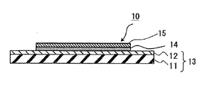
도 1은 본 발명의 실시 형태에 따른 반도체 가공용 테이프의 구조를 모식적으로 도시하는 단면도이다.
도 2는 본 발명의 실시 형태에 따른 반도체 가공용 테이프의 사용 방법을 설명하기 위한 단면도이다.
도 3은 반도체 가공용 테이프를 반도체 웨이퍼 및 링 프레임에 접합하는 장치·방법을 설명하기 위한 도면이다.1 is a cross-sectional view schematically showing the structure of a semiconductor processing tape according to an embodiment of the present invention.
2 is a cross-sectional view for explaining a method of using a semiconductor processing tape according to an embodiment of the present invention.
3 is a view for explaining an apparatus and a method for bonding a semiconductor processing tape to a semiconductor wafer and a ring frame.
이하에, 본 발명의 실시 형태에 대해서 상세하게 설명한다.Hereinafter, embodiments of the present invention will be described in detail.
도 1은, 본 발명의 실시 형태에 따른 반도체 가공용 테이프(10)를 도시하는 단면도이다. 이 반도체 가공용 테이프(10)는, 기재 필름(11)과 기재 필름(11) 상에 설치된 점착제층(12)을 포함하는 다이싱 테이프(13)를 갖고 있으며, 점착제층(12) 상에는, 반도체 칩(C)(도 2 참조)을 보호하기 위한 금속층(14)과, 금속층(14) 상에 설치된 접착제층(15)이 설치되어 있다.1 is a cross-sectional view showing a
접착제층(15)은, 금속층(14)에 접하는 면과는 반대측의 면이 세퍼레이터(박리 라이너)에 의해 보호되어 있는 것이 바람직하다(도시하지 않음). 세퍼레이터는, 실용에 제공될 때까지 접착제층(15)을 보호하는 보호재로서의 기능을 갖고 있다. 또한, 세퍼레이터는, 반도체 가공용 테이프(10)의 제조 과정에서, 다이싱 테이프(13)의 점착제층(12)에 금속층(14)을 접합할 때의 지지 기재로서 사용할 수 있다.It is preferable that the
다이싱 테이프(13), 금속층(14) 및 접착제층(15)은, 사용 공정이나 장치에 맞춰서 미리 소정 형상으로 절단(프리컷)되어 있어도 된다. 또한, 본 발명의 반도체 가공용 테이프(10)는, 반도체 웨이퍼(W) 1매분마다 절단된 형태이어도 되고, 반도체 웨이퍼(W) 1매분마다 절단된 것이 복수 형성된 긴 시트를, 롤 형상으로 권취한 형태이어도 된다. 이하에, 각 구성 요소에 대해서 설명한다.The dicing
<기재 필름(11)>≪ Base material film (11) >
기재 필름(11)으로서는, 다이싱 테이프(13)의 루프 스티프니스가 20mN 이상 200mN 미만으로 되는 것이라면, 종래 공지된 것을 특별히 제한하지 않고 사용할 수 있지만, 후술하는 점착제층(12)으로서 방사선 경화성의 재료를 사용하는 경우에는, 방사선 투과성을 갖는 것을 사용하는 것이 바람직하다.As the
예를 들어, 그 재료로서, 폴리에틸렌, 폴리프로필렌, 에틸렌-프로필렌 공중합체, 폴리부텐-1, 폴리-4-메틸펜텐-1, 에틸렌-아세트산비닐 공중합체, 에틸렌-아크릴산에틸 공중합체, 에틸렌-아크릴산메틸 공중합체, 에틸렌-아크릴산 공중합체, 아이오노머 등의 α-올레핀의 단독 중합체 또는 공중합체 또는 이들의 혼합물, 폴리우레탄, 스티렌-에틸렌-부텐 또는 펜텐계 공중합체, 폴리아미드-폴리올 공중합체 등의 열가소성 엘라스토머 및 이들의 혼합물을 열거할 수 있다. 또한, 기재 필름(11)은, 이들의 군에서 선택되는 2종 이상의 재료가 혼합된 것이어도 되고, 이들이 단층 또는 복층화된 것이어도 된다.Examples of the material include polyethylene, polypropylene, ethylene-propylene copolymer, polybutene-1, poly-4-methylpentene-1, ethylene-vinyl acetate copolymer, ethylene- Homopolymers or copolymers of? -Olefins such as methyl acrylate, methyl acrylate, ethyl acrylate, methyl acrylate, methyl acrylate, methyl acrylate, methyl acrylate, Thermoplastic elastomers, and mixtures thereof. The
기재 필름(11)의 두께는, 특별히 한정되는 것은 아니며, 적절하게 설정해도 되지만, 50 내지 200㎛가 바람직하다.The thickness of the
기재 필름(11)과 점착제층(12)과의 밀착성을 향상시키기 위해서, 기재 필름(11)의 표면에, 크롬산 처리, 오존 폭로, 화염 폭로, 고압 전격 폭로, 이온화 방사선 처리 등의 화학적 또는 물리적 표면 처리를 실시해도 된다.A chemical or physical surface such as chromic acid treatment, ozone exposure, flame exposure, high-voltage electric discharge exposure, and ionizing radiation treatment is applied to the surface of the
또한, 본 실시 형태에서는, 기재 필름(11) 상에 직접적으로 점착제층(12)을 설치했지만, 밀착성을 높이기 위한 프라이머층이나, 다이싱 시의 절삭성 향상을 위한 앵커층, 응력 완화층, 정전 방지층 등을 개재해서 간접적으로 설치해도 된다.Although the pressure sensitive
<점착제층(12)>≪ Pressure-sensitive adhesive layer (12) >
점착제층(12)에 사용되는 수지로서는, 특별히 한정되는 것은 아니며, 점착제에 사용되는 공지된 염소화 폴리프로필렌 수지, 아크릴 수지, 폴리에스테르 수지, 폴리우레탄 수지, 에폭시 수지 등을 사용할 수 있지만, 아크릴계 중합체를 베이스 중합체로 하는 아크릴계 점착제가 바람직하다.The resin used for the pressure-
아크릴계 중합체로서는, 예를 들어 (메트)아크릴산알킬에스테르(예를 들어, 메틸에스테르, 에틸에스테르, 프로필에스테르, 이소프로필에스테르, 부틸에스테르, 이소부틸에스테르, s-부틸에스테르, t-부틸에스테르, 펜틸에스테르, 이소펜틸에스테르, 헥실에스테르, 헵틸에스테르, 옥틸에스테르, 2-에틸헥실에스테르, 이소옥틸에스테르, 노닐에스테르, 데실에스테르, 이소데실에스테르, 운데실에스테르, 도데실에스테르, 트리데실에스테르, 테트라데실에스테르, 헥사데실에스테르, 옥타데실에스테르, 에이코실에스테르 등의 알킬기의 탄소수 1 내지 30, 특히 탄소수 4 내지 18의 직쇄상 또는 분지쇄상의 알킬에스테르 등) 및 (메트)아크릴산시클로알킬에스테르(예를 들어, 시클로펜틸에스테르, 시클로헥실에스테르 등)의 1종 또는 2종 이상을 단량체 성분으로서 사용한 아크릴계 중합체 등을 들 수 있다. 또한, (메트)아크릴산에스테르란, 아크릴산에스테르 및/또는 메타크릴산에스테르를 말하며, 본 발명의 (메트)란 모두 마찬가지의 의미이다.Examples of the acrylic polymer include (meth) acrylic acid alkyl ester (for example, methyl ester, ethyl ester, propyl ester, isopropyl ester, butyl ester, isobutyl ester, s-butyl ester, t-butyl ester, pentyl ester , Isopentyl ester, hexyl ester, heptyl ester, octyl ester, 2-ethylhexyl ester, isooctyl ester, nonyl ester, decyl ester, isodecyl ester, undecyl ester, dodecyl ester, tridecyl ester, Linear or branched alkyl esters having 1 to 30 carbon atoms, particularly 4 to 18 carbon atoms, of alkyl groups such as hexadecyl ester, octadecyl ester and eicosyl ester) and (meth) acrylic acid cycloalkyl esters (for example, Pentyl ester, cyclohexyl ester, etc.) as a monomer component Acrylic polymer used in the present invention. The (meth) acrylate ester refers to an acrylate ester and / or a methacrylate ester, and the (meth) acrylate of the present invention has the same meaning.
아크릴계 중합체는, 응집력, 내열성 등의 개질을 목적으로, 필요에 따라, 상기 (메트)아크릴산알킬에스테르 또는 시클로알킬에스테르와 공중합 가능한 다른 단량체 성분에 대응하는 단위를 포함하고 있어도 된다. 이와 같은 단량체 성분으로서, 예를 들어 아크릴산, 메타크릴산, 카르복시에틸(메트)아크릴레이트, 카르복시펜틸(메트)아크릴레이트, 이타콘산, 말레산, 푸마르산, 크로톤산 등의 카르복실기 함유 단량체; 무수 말레산, 무수 이타콘산 등의 산 무수물 단량체; (메트)아크릴산2-히드록시에틸, (메트)아크릴산2-히드록시프로필, (메트)아크릴산4-히드록시부틸, (메트)아크릴산6-히드록시헥실, (메트)아크릴산8-히드록시옥틸, (메트)아크릴산10-히드록시데실, (메트)아크릴산12-히드록시라우릴, (4-히드록시메틸시클로헥실)메틸(메트)아크릴레이트 등의 히드록실기 함유 단량체; 스티렌술폰산, 알릴술폰산, 2-(메트)아크릴아미드-2-메틸프로판술폰산, (메트)아크릴아미도프로판술폰산, 술포프로필(메트)아크릴레이트, (메트)아크릴로일옥시나프탈렌술폰산 등의 술폰산기 함유 단량체; 2-히드록시에틸아크릴로일포스페이트 등의 인산기 함유 단량체; 아크릴아미드, 아크릴로니트릴 등을 들 수 있다. 이들 공중합 가능한 단량체 성분은, 1종 또는 2종 이상 사용할 수 있다. 이들 공중합 가능한 단량체의 사용량은, 전체 단량체 성분의 40중량% 이하가 바람직하다.The acrylic polymer may contain units corresponding to other monomer components copolymerizable with the (meth) acrylic acid alkyl ester or the cycloalkyl ester, if necessary, for the purpose of modifying the cohesive force, heat resistance and the like. Examples of such monomer components include carboxyl group-containing monomers such as acrylic acid, methacrylic acid, carboxyethyl (meth) acrylate, carboxypentyl (meth) acrylate, itaconic acid, maleic acid, fumaric acid and crotonic acid; Acid anhydride monomers such as maleic anhydride and itaconic anhydride; Acrylate such as 2-hydroxyethyl (meth) acrylate, 2-hydroxypropyl (meth) acrylate, 4-hydroxybutyl (meth) acrylate, 6-hydroxyhexyl (meth) acrylate, Hydroxy group-containing monomers such as (meth) acrylic acid 10-hydroxydecyl, (meth) acrylic acid 12-hydroxylauryl and (4-hydroxymethylcyclohexyl) methyl (meth) acrylate; Sulfonic acid groups such as styrenesulfonic acid, allylsulfonic acid, 2- (meth) acrylamide-2-methylpropanesulfonic acid, (meth) acrylamidopropanesulfonic acid, sulfopropyl (meth) acrylate, and (meth) acryloyloxynaphthalenesulfonic acid Containing monomer; Phosphoric acid group-containing monomers such as 2-hydroxyethyl acryloyl phosphate; Acrylamide, acrylonitrile, and the like. These copolymerizable monomer components may be used alone or in combination of two or more. The amount of these copolymerizable monomers to be used is preferably 40% by weight or less based on the total monomer components.
또한, 아크릴계 중합체는, 가교되기 때문에, 다관능성 단량체 등도 필요에 따라서 공중합용 단량체 성분으로서 포함할 수 있다. 이와 같은 다관능성 단량체로서, 예를 들어 헥산디올디(메트)아크릴레이트, (폴리)에틸렌글리콜디(메트)아크릴레이트, (폴리)프로필렌글리콜디(메트)아크릴레이트, 네오펜틸글리콜디(메트)아크릴레이트, 펜타에리트리톨디(메트)아크릴레이트, 트리메틸올프로판트리(메트)아크릴레이트, 펜타에리트리톨트리(메트)아크릴레이트, 디펜타에리트리톨헥사(메트)아크릴레이트, 에폭시(메트)아크릴레이트, 폴리에스테르(메트)아크릴레이트, 우레탄(메트)아크릴레이트 등을 들 수 있다. 이들 다관능성 단량체도 1종 또는 2종 이상 사용할 수 있다. 다관능성 단량체의 사용량은, 점착 특성 등의 점에서, 전체 단량체 성분의 30중량% 이하가 바람직하다.Further, since the acrylic polymer is crosslinked, a polyfunctional monomer and the like can be included as a monomer component for copolymerization as needed. Examples of such polyfunctional monomers include hexanediol di (meth) acrylate, (poly) ethylene glycol di (meth) acrylate, (poly) propylene glycol di (meth) acrylate, neopentyl glycol di Acrylate, dipentaerythritol hexa (meth) acrylate, epoxy (meth) acrylate, pentaerythritol tri (meth) acrylate, pentaerythritol tri , Polyester (meth) acrylate, and urethane (meth) acrylate. These polyfunctional monomers may be used singly or in combination of two or more. The amount of the multifunctional monomer to be used is preferably 30% by weight or less based on the total amount of the monomer components from the viewpoint of adhesion properties and the like.
아크릴계 중합체의 제조는, 예를 들어 1종 또는 2종 이상의 성분 단량체의 혼합물에 용액 중합 방식이나 유화 중합 방식, 괴상 중합 방식이나 현탁 중합 방식 등의 적절한 방식을 적용해서 행할 수 있다. 점착제층(12)은, 웨이퍼의 오염 방지 등의 점에서, 저분자량 물질의 함유를 억제한 조성이 바람직하고, 이러한 점에서 중량 평균 분자량이 30만 이상, 특히 40만 내지 300만의 아크릴계 중합체를 주성분으로 하는 것이 바람직하므로, 점착제는, 내부 가교 방식이나 외부 가교 방식 등에 의한 적절한 가교 타입으로 할 수도 있다.The acrylic polymer can be produced, for example, by applying a suitable method such as a solution polymerization method, an emulsion polymerization method, a bulk polymerization method or a suspension polymerization method to a mixture of one kind or two or more kinds of component monomers. The pressure-
또한, 점착제층(12)의 가교 밀도의 제어를 위해서, 예를 들어 다관능 이소시아네이트계 화합물, 다관능 에폭시계 화합물, 멜라민계 화합물, 금속염계 화합물, 금속 킬레이트계 화합물, 아미노 수지계 화합물, 또는 과산화물 등의 적절한 외부 가교제를 사용해서 가교 처리하는 방식이나, 탄소-탄소 이중 결합을 2개 이상 갖는 저분자 화합물을 혼합해서 에너지선의 조사 등에 의해 가교 처리하는 방식 등의 적합한 방식을 채용할 수 있다. 외부 가교제를 사용하는 경우, 그 사용량은, 가교해야 할 베이스 중합체와의 밸런스에 따라, 나아가 점착제로서의 사용 용도에 따라 적절히 결정된다. 일반적으로는, 상기 베이스 중합체 100중량부에 대하여 5중량부 정도 이하, 또한 0.1중량부 내지 5중량부 배합하는 것이 바람직하다. 또한, 점착제에는, 필요에 따라, 상기 성분 외에, 각종 점착 부여제, 노화 방지제 등의 첨가제를 사용해도 된다.For controlling the crosslinking density of the pressure-
점착제층(12)을 구성하는 점착제로서는, 방사선 경화형 점착제가 적합하다. 방사선 경화형 점착제로서는, 상술한 점착제에, 방사선 경화성의 단량체 성분이나 방사선 경화성의 올리고머 성분을 배합한 첨가형의 방사선 경화형 점착제를 예시할 수 있다.As the pressure-sensitive adhesive constituting the pressure-
배합하는 방사선 경화성의 단량체 성분으로서는, 예를 들어 우레탄(메트)아크릴레이트, 트리메틸올프로판트리(메트)아크릴레이트, 테트라메틸올메탄테트라(메트)아크릴레이트, 펜타에리트리톨트리(메트)아크릴레이트, 펜타에리트리톨테트라(메트)아크릴레이트, 디펜타에리트리톨모노히드록시펜타(메트)아크릴레이트, 디펜타에리트리톨헥사(메트)아크릴레이트, 1,4-부탄디올디(메트)아크릴레이트 등을 들 수 있다. 이들 단량체 성분은, 1종 또는 2종 이상 병용할 수 있다.Examples of radiation curable monomer components to be blended include urethane (meth) acrylate, trimethylolpropane tri (meth) acrylate, tetramethylolmethane tetra (meth) acrylate, pentaerythritol tri (Meth) acrylate, pentaerythritol tetra (meth) acrylate, dipentaerythritol monohydroxypenta (meth) acrylate, dipentaerythritol hexa (meth) acrylate and 1,4-butanediol di have. These monomer components may be used alone or in combination of two or more.
또한, 방사선 경화성의 올리고머 성분은, 우레탄계, 폴리에테르계, 폴리에스테르계, 폴리카르보네이트계, 폴리부타디엔계 등 다양한 올리고머를 들 수 있으며, 그 분자량이 100 내지 30000 정도의 범위의 것이 적당하다. 방사선 경화성의 단량체 성분이나 올리고머 성분의 배합량은, 상기 점착제층의 종류에 따라, 점착제층의 점착력을 저하시킬 수 있는 양을, 적절하게 결정할 수 있다. 일반적으로는, 점착제를 구성하는 아크릴계 중합체 등의 베이스 중합체 100중량부에 대하여, 예를 들어 5중량부 내지 500중량부, 바람직하게는 70중량부 내지 150중량부 정도이다.Examples of the radiation-curable oligomer component include urethane-based, polyether-based, polyester-based, polycarbonate-based, and polybutadiene-based oligomers. The molecular weight of the oligomer is suitably in the range of about 100 to 30,000. The amount of the radiation-curable monomer component or the oligomer component can be appropriately determined depending on the type of the pressure-sensitive adhesive layer so as to lower the adhesive force of the pressure-sensitive adhesive layer. Generally, the amount is, for example, about 5 parts by weight to 500 parts by weight, and preferably about 70 parts by weight to 150 parts by weight, relative to 100 parts by weight of the base polymer such as acrylic polymer constituting the pressure-sensitive adhesive.
또한, 방사선 경화형 점착제로서는, 상기 첨가형의 방사선 경화형 점착제 이외에, 베이스 중합체로서 탄소-탄소 이중 결합을 중합체 측쇄 또는 주쇄 중 또는 주쇄 말단에 갖는 것을 사용한 내재형 방사선 경화형 점착제도 들 수 있다. 내재형 방사선 경화형 점착제는, 저분자 성분인 올리고머 성분 등을 함유할 필요가 없거나, 또는 많이 포함하지 않기 때문에, 경시적으로 올리고머 성분 등이 점착제 재중을 이동하지 않고, 안정된 층 구조의 점착제층을 형성할 수 있기 때문에 바람직하다.As the radiation curing type pressure-sensitive adhesive, in addition to the radiation curing type pressure-sensitive adhesive of the above-mentioned addition type, an internal type radiation curing type pressure-sensitive adhesive using a base polymer having a carbon-carbon double bond at the polymer side chain, main chain or main chain terminal thereof. Since the intrinsic type radiation-curable pressure-sensitive adhesive does not need to contain an oligomer component or the like, which is a low-molecular component, or the like, it does not contain a large amount of oligomer component or the like and therefore an oligomer component or the like does not migrate with time and forms a pressure- It is preferable.
탄소-탄소 이중 결합을 갖는 베이스 중합체는, 탄소-탄소 이중 결합을 갖고, 또한 점착성을 갖는 것을 특별히 제한 없이 사용할 수 있다. 이와 같은 베이스 중합체로서는, 아크릴계 중합체를 기본 골격으로 하는 것이 바람직하다. 아크릴계 중합체의 기본 골격으로서는, 상기 예시한 아크릴계 중합체를 들 수 있다.The base polymer having a carbon-carbon double bond may be a polymer having a carbon-carbon double bond and having a sticking property without particular limitation. As such a base polymer, an acrylic polymer is preferably used as a basic skeleton. As the basic skeleton of the acrylic polymer, there may be mentioned the acrylic polymer exemplified above.
아크릴계 중합체에의 탄소-탄소 이중 결합의 도입법은 특별히 제한되지 않고, 다양한 방법을 채용할 수 있지만, 탄소-탄소 이중 결합은, 중합체 측쇄에 도입하는 것이 분자 설계 상 용이하다. 예를 들어, 미리, 아크릴계 중합체에 관능기를 갖는 단량체를 공중합한 후, 이 관능기와 반응할 수 있는 관능기 및 탄소-탄소 이중 결합을 갖는 화합물을, 탄소-탄소 이중 결합의 방사선 경화성을 유지한 채 축합 또는 부가 반응시키는 방법을 들 수 있다.A method for introducing a carbon-carbon double bond to an acrylic polymer is not particularly limited, and various methods can be adopted. However, it is easy to introduce a carbon-carbon double bond into a side chain of a polymer in terms of molecular design. For example, after a monomer having a functional group is copolymerized with an acrylic polymer in advance, a compound having a functional group capable of reacting with the functional group and a carbon-carbon double bond is condensed Or an addition reaction is carried out.
이들 관능기의 조합의 예로서는, 카르복실산기와 에폭시기, 카르복실산기와 아지리딜기, 히드록실기와 이소시아네이트기 등을 들 수 있다. 이들 관능기의 조합 중에서도 반응 추적의 용이함 면에서, 히드록실기와 이소시아네이트기의 조합이 적합하다. 또한, 이들 관능기의 조합에 의해, 상기 탄소-탄소 이중 결합을 갖는 아크릴계 중합체를 생성하는 조합이라면, 관능기는 아크릴계 중합체와 상기 화합물의 어느 측에 있어도 되지만, 상기 바람직한 조합에서는, 아크릴계 중합체가 히드록실기를 갖고, 상기 화합물이 이소시아네이트기를 갖는 경우가 적합하다. 이 경우, 탄소-탄소 이중 결합을 갖는 이소시아네이트 화합물로서는, 예를 들어 메타크릴로일이소시아네이트, 2-메타크릴로일옥시에틸이소시아네이트, m-이소프로페닐-α,α-디메틸벤질이소시아네이트 등을 들 수 있다. 또한, 아크릴계 중합체로서는, 상기 예시한 히드록시기 함유 단량체나 2-히드록시에틸비닐에테르, 4-히드록시부틸비닐에테르, 디에틸렌글리콜모노비닐에테르의 에테르계 화합물 등을 공중합한 것이 사용된다.Examples of combinations of these functional groups include a carboxylic acid group and an epoxy group, a carboxylic acid group and an aziridyl group, and a hydroxyl group and an isocyanate group. Among these combinations of functional groups, a combination of a hydroxyl group and an isocyanate group is preferable in terms of ease of reaction tracking. In the combination of these functional groups, the functional group may be present on either side of the acrylic polymer and the compound, provided that the acrylic polymer having the carbon-carbon double bond is produced. In the preferred combination, the acrylic polymer is a hydroxyl group , And the compound has an isocyanate group. In this case, examples of the isocyanate compound having a carbon-carbon double bond include methacryloyl isocyanate, 2-methacryloyloxyethyl isocyanate, m-isopropenyl- ?,? -Dimethylbenzyl isocyanate and the like have. As the acrylic polymer, a copolymer obtained by copolymerizing the above-exemplified hydroxyl group-containing monomer, 2-hydroxyethyl vinyl ether, 4-hydroxybutyl vinyl ether, and ether compound of diethylene glycol monovinyl ether is used.
내재형 방사선 경화형 점착제는, 상기 탄소-탄소 이중 결합을 갖는 베이스 중합체(특히 아크릴계 중합체)를 단독으로 사용할 수 있지만, 특성을 악화시키지 않을 정도로 상기 방사선 경화성의 단량체 성분이나 올리고머 성분 등의 광중합성 화합물을 배합할 수도 있다. 당해 광중합성 화합물의 배합량은, 통상 베이스 중합체 100중량부에 대하여 30중량부 이하의 범위 내이며, 바람직하게는 0 내지 10중량부의 범위 내이다.The intrinsic type radiation-curable pressure-sensitive adhesive can use the above-mentioned base polymer (in particular acrylic polymer) having a carbon-carbon double bond alone, but it is also possible to use a photopolymerizable compound such as the above radiation curable monomer component or oligomer component It may be blended. The compounding amount of the photopolymerizable compound is usually within a range of 30 parts by weight or less, preferably from 0 to 10 parts by weight, based on 100 parts by weight of the base polymer.
방사선 경화형 점착제에는, 자외선 등에 의해 경화시킨 경우에는 광중합 개시제를 함유시키는 것이 바람직하다.When the radiation-curing pressure-sensitive adhesive is cured by ultraviolet rays or the like, it is preferable to include a photopolymerization initiator.
상술한 아크릴계 중합체 중에서도, 특히 CH2=CHCOOR(식 중, R은 탄소수가 4 내지 8인 알킬기임)로 표현되는 아크릴산에스테르와, 히드록실기 함유 단량체와, 분자 내에 라디칼 반응성 탄소-탄소 이중 결합을 갖는 이소시아네이트 화합물을 포함하는 아크릴계 중합체 A가 바람직하다.Among the above-mentioned acrylic polymers, acrylate esters represented by CH 2 CHCOOR (wherein R is an alkyl group having 4 to 8 carbon atoms), hydroxyl group-containing monomers and radical-reactive carbon-carbon double bonds Is preferably an acrylic polymer A containing an isocyanate compound.
아크릴산알킬에스테르의 알킬기의 탄소수가 4 미만이면, 박리력이 너무 커져서 픽업성이 저하되는 경우가 있다. 한편, 아크릴산알킬에스테르의 알킬기의 탄소수가 8을 초과하면, 금속층(15)과의 접착성 또는 밀착성이 저하되고, 그 결과, 다이싱 시에 금속층(15)의 박리가 발생하는 경우가 있다.If the number of carbon atoms in the alkyl group of the alkyl acrylate is less than 4, the peeling force becomes too large and the pick-up property may be lowered. On the other hand, when the number of carbon atoms in the alkyl group of the alkyl acrylate is more than 8, the adhesion or adhesiveness with the
상기 아크릴계 중합체 A는, 필요에 따라, 다른 단량체 성분에 대응하는 단위를 포함하고 있어도 된다.The acrylic polymer A may contain units corresponding to other monomer components, if necessary.
아크릴계 중합체 A에서는, 라디칼 반응성 탄소-탄소 이중 결합을 갖는 이소시아네이트 화합물이 사용된다. 즉, 아크릴 중합체는, 상기 아크릴산에스테르나 히드록실기 함유 단량체 등의 단량체 조성물에 의한 중합체에, 이중 결합 함유 이소시아네이트 화합물이 부가 반응된 구성을 갖고 있는 것이 바람직하다. 따라서, 아크릴계 중합체는, 그 분자 구조 내에, 라디칼 반응성 탄소-탄소 이중 결합을 갖고 있는 것이 바람직하다. 이에 의해, 활성 에너지선(자외선 등)의 조사에 의해 경화하는 활성 에너지선 경화형 점착제층(자외선 경화형 점착제층 등)으로 할 수 있어, 금속층(15)과 점착제층(12)과의 박리력을 저하시킬 수 있다.In the acrylic polymer A, an isocyanate compound having a radical reactive carbon-carbon double bond is used. That is, it is preferable that the acrylic polymer has a structure in which a double bond-containing isocyanate compound is additionally reacted with a polymer obtained by a monomer composition such as an acrylic acid ester or a hydroxyl group-containing monomer. Therefore, it is preferable that the acrylic polymer has a radical reactive carbon-carbon double bond in its molecular structure. This makes it possible to form an active energy ray-curable pressure-sensitive adhesive layer (ultraviolet-curable pressure-sensitive adhesive layer or the like) which is cured by irradiation of an active energy ray (ultraviolet ray or the like), thereby lowering the peeling force between the
이중 결합 함유 이소시아네이트 화합물로서는, 예를 들어 메타크릴로일이소시아네이트, 아크릴로일이소시아네이트, 2-메타크릴로일옥시에틸이소시아네이트, 2-아크릴로일옥시에틸이소시아네이트, m-이소프로페닐-α,α-디메틸벤질이소시아네이트 등을 들 수 있다. 이중 결합 함유 이소시아네이트 화합물은, 단독으로 또는 2종 이상을 조합해서 사용할 수 있다.Examples of the double bond-containing isocyanate compound include methacryloyl isocyanate, acryloyl isocyanate, 2-methacryloyloxyethyl isocyanate, 2-acryloyloxyethyl isocyanate, m- Dimethyl benzyl isocyanate and the like. The double bond-containing isocyanate compounds may be used alone or in combination of two or more.
또한, 활성 에너지선 경화형 점착제에는, 활성 에너지선 조사 전의 점착력이나, 활성 에너지선 조사 후의 점착력을 조정하기 위해서, 외부 가교제를 적절하게 사용할 수도 있다. 외부 가교 방법의 구체적 수단으로서는, 폴리이소시아네이트 화합물, 에폭시 화합물, 아지리딘 화합물, 멜라민계 가교제 등의 소위 가교제를 첨가해서 반응시키는 방법을 들 수 있다. 외부 가교제를 사용하는 경우, 그 사용량은, 가교해야 할 베이스 중합체와의 밸런스에 따라, 나아가 점착제로서의 사용 용도에 따라 적절히 결정된다. 외부 가교제의 사용량은, 일반적으로는, 상기 베이스 중합체 100중량부에 대하여 20중량부 이하(바람직하게는 0.1중량부 내지 10중량부)이다. 또한, 활성 에너지선 경화형 점착제에는, 필요에 따라, 상기 성분 외에, 종래 공지된 각종 점착 부여제, 노화 방지제, 발포제 등의 첨가제가 배합되어 있어도 된다.In addition, an external crosslinking agent may be suitably used in the active energy ray-curable pressure-sensitive adhesive in order to adjust the adhesive strength before irradiation with active energy rays or the adhesive force after irradiation with active energy rays. Specific examples of the external crosslinking method include a method in which a so-called crosslinking agent such as a polyisocyanate compound, an epoxy compound, an aziridine compound, or a melamine crosslinking agent is added and reacted. When an external crosslinking agent is used, the amount thereof to be used is appropriately determined according to the balance with the base polymer to be crosslinked, and furthermore, according to the intended use as an adhesive. The amount of the external crosslinking agent to be used is generally 20 parts by weight or less (preferably 0.1 part by weight to 10 parts by weight) based on 100 parts by weight of the base polymer. The active energy ray-curable pressure-sensitive adhesive may contain, if necessary, additives such as various known tackifiers, anti-aging agents, and foaming agents in addition to the above components.
점착제층(12)의 두께는, 특별히 제한되지 않고 적절하게 결정할 수 있지만, 일반적으로는 5 내지 200㎛ 정도이다. 또한, 점착제층(12)은 단층을 포함하고 있어도 복수층을 포함하고 있어도 된다.The thickness of the pressure-
다이싱 테이프(13)의 두께는, 취급성의 관점에서 55㎛ 이상이 바람직하고, 반도체 가공용 테이프의 강도를 높이는 관점에서 70㎛ 이상이 바람직하다. 또한, 다이싱 후에 익스팬드가 필요하므로 215㎛ 미만이 바람직하고, 픽업성이 우수한 관점에서 160㎛ 미만이 바람직하다.The thickness of the dicing
다이싱 테이프(13)는, 하기의 조건 하에서 측정한 루프 스티프니스가 20mN 이상 200mN 미만이고, 바람직하게는 26mN 이상, 보다 바람직하게는 33mN 이상이다.The dicing
루프 스티프니스 측정 조건:Loop Stiffness Measurement conditions:
장치; 루프 스티프니스 테스터 DA(도요 세끼 가부시끼가이샤 제조, 상품명)Device; Loop Stiffness Tester DA (trade name, manufactured by TOYO SEKI KABUSHIKI KAISHA)
루프(샘플) 형상; 길이 80mm, 폭 25mmLoop (sample) shape; Length 80mm, width 25mm
압자의 압입 속도; 3.3mm/secIndentation speed of indenter; 3.3mm / sec
측정 데이터; 폭 25mm로 잘라낸 다이싱 테이프의 시험편을 점착제층이 부착되어 있는 표면이 루프의 내측이 되도록 Ω자 형상의 루프형으로 구부린 다음, 그 길이 방향의 양단을 겹쳐서, 루프의 둘레 길이가 80mm가 되도록 그 겹친 부분을 척으로 파지하였다. 시험편을 루프가 환 형상이 되도록 고정하고, 그 루프를 압축 속도 3.3mm/sec으로, 압자가 루프와 접촉한 시점에서부터 10mm 압입했을 때 로드셀에 검출되는 부하 하중값을 구함으로써 측정한다.Measurement data; A test piece of a dicing tape cut into a width of 25 mm was bent into a loop shape having an Ω shape so that the surface with the adhesive layer on the inner side of the loop was overlapped and both ends in the longitudinal direction thereof were overlapped, The overlapped portion was gripped with a chuck. The test piece is fixed to the loop so that the loop is annular and the loop is measured at a compression rate of 3.3 mm / sec by calculating the load load value detected on the load cell when the indenter is pressed 10 mm from the point of contact with the loop.
다이싱 테이프(13)의 루프 스티프니스를 20mN 이상으로 함으로써, 반도체 가공용 테이프(10)를 반도체 웨이퍼(W)에 접합하는 가장 초기 단계에서, 다이싱 테이프(13)의 선단만이 링 프레임에 고정되고, 나머지 부분이 세퍼레이터와 함께, 도 3에서의 C 방향으로 인장되었다고 해도, 다이싱 테이프(10)가 변형되어 신장되는 것을 방지할 수 있다. 이 때문에, 다이싱 테이프(10) 및 그 위에 설치되어 있는 금속층(14), 접착제층(15)에 주름이 발생하는 것을 방지할 수 있다. 다이싱 테이프(13)의 루프 스티프니스를 200mN 이상으로 하면, 반도체 가공용 테이프(10)에 접합된 반도체 웨이퍼(W)를 칩 형상으로 개편화(다이싱)한 후, 개편화된 반도체 칩(C)을 픽업할 때, 밀어올림 핀에 의해 기재 필름(11)측으로부터 반도체 칩(C)을 밀어올렸을 때, 금속층(14)과 점착제층(12)과의 사이에 충분한 박리 계기가 생기지 않아, 반도체 칩(C)을 양호하게 픽업할 수 없다.The loop stiffness of the dicing
<금속층(14)>≪
금속층(14)을 구성하는 금속으로서는 특별히 한정되지 않고, 예를 들어, 알루미늄, 철, 티타늄, 주석, 니켈 및 구리로 이루어지는 군에서 선택되는 적어도 1종의 금속 및/또는 그들의 합금인 것이, 레이저 마킹성의 면에서 바람직하다. 이들 중에서도, 구리, 알루미늄 또는 그들의 합금은 열전도성이 높아, 금속층을 개재한 방열의 효과를 얻을 수 있다. 또한, 구리, 알루미늄, 철, 니켈 또는 그들의 합금은, 전자 디바이스 패키지의 휨 억제 효과도 얻을 수 있다.The metal constituting the
금속층(14)의 두께는, 반도체 웨이퍼(W) 또는 반도체 칩(C)의 취급성 및 가공성 등을 고려해서 적절히 결정할 수 있으며, 통상 2 내지 200㎛의 범위이며, 3 내지 100㎛인 것이 바람직하고, 4 내지 80㎛인 것이 보다 바람직하고, 5 내지 50㎛인 것이 특히 바람직하다. 금속층은 200㎛ 이상이 되면 권취가 곤란해지고, 50㎛ 이상이 되면 가공성의 문제로 생산성이 저하된다. 한편, 취급성의 관점에서 최저 2㎛ 이상이 필요하다.The thickness of the
<접착제층(15)>≪ Adhesive layer (15) >
접착제층(15)은, 접착제를 미리 필름화한 것이다.The adhesive layer (15) is a film obtained by previously laminating an adhesive.
접착제층(15)은, 적어도 열경화성 수지에 의해 형성되어 있고, 적어도 열경화성 수지와 열가소성 수지에 의해 형성되어 있는 것이 바람직하다.The
열가소성 수지로서는, 예를 들어 천연 고무, 부틸 고무, 이소프렌 고무, 클로로프렌 고무, 에틸렌-아세트산비닐 공중합체, 에틸렌-아크릴산 공중합체, 에틸렌-아크릴산에스테르 공중합체, 폴리부타디엔 수지, 폴리카르보네이트 수지, 열가소성 폴리이미드 수지, 6-나일론이나 6,6-나일론 등의 폴리아미드 수지, 페녹시 수지, 아크릴 수지, PET(폴리에틸렌테레프탈레이트)나 PBT(폴리부틸렌테레프탈레이트) 등의 포화 폴리에스테르 수지, 폴리아미드이미드 수지, 또는 불소 수지 등을 들 수 있다. 열가소성 수지는 단독으로 또는 2종 이상을 병용해서 사용할 수 있다. 이들 열가소성 수지 중, 이온성 불순물이 적고 내열성이 높아, 반도체 소자의 신뢰성을 확보할 수 있는 아크릴 수지가 특히 바람직하다.Examples of the thermoplastic resin include natural rubber, butyl rubber, isoprene rubber, chloroprene rubber, ethylene-vinyl acetate copolymer, ethylene-acrylic acid copolymer, ethylene-acrylic acid ester copolymer, polybutadiene resin, polycarbonate resin, A polyimide resin, a polyamide resin such as 6-nylon or 6,6-nylon, a phenoxy resin, an acrylic resin, a saturated polyester resin such as PET (polyethylene terephthalate) or PBT (polybutylene terephthalate) Amide resin, or a fluorine resin. The thermoplastic resin may be used alone or in combination of two or more. Of these thermoplastic resins, an acrylic resin which is low in ionic impurities and high in heat resistance and can ensure the reliability of a semiconductor element is particularly preferable.
아크릴 수지로서는, 특별히 한정되는 것은 아니며, 탄소수 30 이하(바람직하게는 탄소수 4 내지 18, 더욱 바람직하게는 탄소수 6 내지 10, 특히 바람직하게는 탄소수 8 또는 9)의 직쇄 또는 분지의 알킬기를 갖는 아크릴산 또는 메타크릴산의 에스테르의 1종 또는 2종 이상을 성분으로 하는 중합체 등을 들 수 있다. 즉, 본 발명에서는, 아크릴 수지란, 메타크릴 수지도 포함하는 광의의 의미이다. 상기 알킬기로서는, 예를 들어 메틸기, 에틸기, 프로필기, 이소프로필기, n-부틸기, t-부틸기, 이소부틸기, 펜틸기, 이소펜틸기, 헥실기, 헵틸기, 2-에틸헥실기, 옥틸기, 이소옥틸기, 노닐기, 이소노닐기, 데실기, 이소데실기, 운데실기, 도데실기(라우릴기), 트리데실기, 테트라데실기, 스테아릴기, 옥타데실기 등을 들 수 있다.The acrylic resin is not particularly limited and acrylic acid having a linear or branched alkyl group having 30 or less carbon atoms (preferably 4 to 18 carbon atoms, more preferably 6 to 10 carbon atoms, particularly preferably 8 or 9 carbon atoms) And polymers containing one or more kinds of esters of methacrylic acid as a component. That is, in the present invention, an acrylic resin means a broad sense including a methacrylic resin. Examples of the alkyl group include a methyl group, an ethyl group, a propyl group, an isopropyl group, an n-butyl group, a t-butyl group, an isobutyl group, a pentyl group, an isopentyl group, a hexyl group, (Lauryl group), a tridecyl group, a tetradecyl group, a stearyl group, an octadecyl group, and the like may be optionally substituted with one or more substituents selected from the group consisting of an alkyl group, an alkenyl group, an alkynyl group, .
또한, 아크릴 수지를 형성하기 위한 다른 단량체(알킬기의 탄소수가 30 이하인 아크릴산 또는 메타크릴산의 알킬에스테르 이외의 단량체)로서는, 특별히 한정되는 것은 아니며, 예를 들어 아크릴산, 메타크릴산, 카르복시에틸아크릴레이트, 카르복시펜틸아크릴레이트, 이타콘산, 말레산, 푸마르산 또는 크로톤산 등과 같은 카르복실기 함유 단량체, 무수 말레산 또는 무수 이타콘산 등과 같은 산 무수물 단량체, (메트)아크릴산2-히드록시에틸, (메트)아크릴산2-히드록시프로필, (메트)아크릴산4-히드록시부틸, (메트)아크릴산6-히드록시헥실, (메트)아크릴산8-히드록시옥틸, (메트)아크릴산10-히드록시데실, (메트)아크릴산12-히드록시라우릴 또는 (4-히드록시메틸시클로헥실)-메틸아크릴레이트 등과 같은 히드록실기 함유 단량체, 스티렌술폰산, 알릴술폰산, 2-(메트)아크릴아미드-2-메틸프로판술폰산, (메트)아크릴아미도프로판술폰산, 술포프로필(메트)아크릴레이트 또는 (메트)아크릴로일옥시나프탈렌술폰산 등과 같은 술폰산기 함유 단량체, 또는 2-히드록시에틸아크릴로일포스페이트 등과 같은 인산기 함유 단량체 등을 들 수 있다. 또한, (메트)아크릴산이란 아크릴산 및/또는 메타크릴산을 말하며, 본 발명의 (메트)란 모두 마찬가지의 의미이다.Further, other monomers (monomers other than acrylic acid or alkyl ester of methacrylic acid having an alkyl group of 30 or less in the alkyl group) for forming an acrylic resin are not particularly limited, and examples thereof include acrylic acid, methacrylic acid, carboxyethyl acrylate (Meth) acrylate, 2-hydroxyethyl (meth) acrylate, 2-hydroxyethyl (meth) acrylate, 2-hydroxypropyl (meth) acrylate and the like; acid anhydride monomers such as carboxypentyl acrylate, itaconic acid, maleic acid, fumaric acid or crotonic acid, (Meth) acrylate, 10-hydroxydecyl (meth) acrylate, 6-hydroxybutyl (meth) acrylate, - hydroxyl group-containing monomers such as hydroxylauryl or (4-hydroxymethylcyclohexyl) -methylacrylate, styrenesulfonic acid, allylsulfonic acid, Sulfonic acid group-containing monomers such as 2- (meth) acrylamide-2-methylpropanesulfonic acid, (meth) acrylamidopropanesulfonic acid, sulfopropyl (meth) acrylate or (meth) acryloyloxynaphthalenesulfonic acid, And phosphoric acid group-containing monomers such as hydroxyethyl acryloyl phosphate and the like. Further, (meth) acrylic acid refers to acrylic acid and / or methacrylic acid, and (meth) in the present invention means the same.
또한, 열경화성 수지로서는, 에폭시 수지, 페놀 수지 외에, 아미노 수지, 불포화 폴리에스테르 수지, 폴리우레탄 수지, 실리콘 수지, 열경화성 폴리이미드 수지 등을 들 수 있다. 열경화성 수지는, 단독으로 또는 2종 이상 병용해서 사용할 수 있다. 열경화성 수지로서는, 특히, 반도체 소자를 부식시키는 이온성 불순물 등 함유가 적은 에폭시 수지가 적합하다. 또한, 에폭시 수지의 경화제로서는 페놀 수지를 적합하게 사용할 수 있다.Examples of the thermosetting resin include an amino resin, an unsaturated polyester resin, a polyurethane resin, a silicone resin and a thermosetting polyimide resin in addition to an epoxy resin and a phenol resin. The thermosetting resins may be used alone or in combination of two or more. As the thermosetting resin, an epoxy resin having a small content of ionic impurities which corrodes semiconductor elements is particularly suitable. As the curing agent of the epoxy resin, a phenol resin can be suitably used.
에폭시 수지로서는, 특별히 한정은 없고, 예를 들어 비스페놀 A형 에폭시 수지, 비스페놀 F형 에폭시 수지, 비스페놀 S형 에폭시 수지, 브롬화비스페놀 A형 에폭시 수지, 수소 첨가 비스페놀 A형 에폭시 수지, 비스페놀 AF형 에폭시 수지, 비페닐형 에폭시 수지, 나프탈렌형 에폭시 수지, 플루올렌형 에폭시 수지, 페놀노볼락형 에폭시 수지, 오르토크레졸노볼락형 에폭시 수지, 트리스히드록시페닐메탄형 에폭시 수지, 테트라페닐올에탄형 에폭시 수지 등의 2관능 에폭시 수지나 다관능 에폭시 수지, 또는 히단토인형 에폭시 수지, 트리스글리시딜이소시아누레이트형 에폭시 수지 또는 글리시딜아민형 에폭시 수지 등의 에폭시 수지를 사용할 수 있다.Examples of the epoxy resin include, but not limited to, bisphenol A type epoxy resin, bisphenol F type epoxy resin, bisphenol S type epoxy resin, brominated bisphenol A type epoxy resin, hydrogenated bisphenol A type epoxy resin, bisphenol AF type epoxy resin , Biphenyl type epoxy resin, naphthalene type epoxy resin, fluorene type epoxy resin, phenol novolak type epoxy resin, orthocresol novolak type epoxy resin, trishydroxyphenyl methane type epoxy resin, tetraphenylol ethane type epoxy resin, etc. Epoxy resin such as bifunctional epoxy resin, polyfunctional epoxy resin, hydantoin type epoxy resin, trisglycidyl isocyanurate type epoxy resin or glycidylamine type epoxy resin can be used.
에폭시 수지로서는, 예시 중 노볼락형 에폭시 수지, 비페닐형 에폭시 수지, 트리스히드록시페닐메탄형 에폭시 수지, 테트라페닐올에탄형 에폭시 수지가 특히 바람직하다. 이들 에폭시 수지는, 경화제로서의 페놀 수지와의 반응성이 많고, 내열성 등이 우수하기 때문이다.As the epoxy resin, novolak type epoxy resin, biphenyl type epoxy resin, trishydroxyphenylmethane type epoxy resin and tetraphenylol ethane type epoxy resin are particularly preferable. These epoxy resins are excellent in reactivity with a phenol resin as a curing agent and excellent in heat resistance and the like.
또한, 페놀 수지는, 에폭시 수지의 경화제로서 작용하는 것이며, 예를 들어 페놀노볼락 수지, 페놀아르알킬 수지, 크레졸노볼락 수지, tert-부틸페놀노볼락 수지, 노닐페놀노볼락 수지 등의 노볼락형 페놀 수지, 레졸형 페놀 수지, 폴리파라옥시스티렌 등의 폴리옥시스티렌 등을 들 수 있다. 페놀 수지는 단독으로 또는 2종 이상을 병용해서 사용할 수 있다. 이들 페놀 수지 중 페놀노볼락 수지, 페놀아르알킬 수지가 특히 바람직하다. 반도체 장치의 접속 신뢰성을 향상시킬 수 있기 때문이다.The phenol resin acts as a curing agent for an epoxy resin. Examples thereof include phenol novolac resins, phenol aralkyl resins, cresol novolac resins, tert-butylphenol novolac resins, novolac phenol novolak resins, Type phenol resin, resole-type phenol resin, and polyoxystyrene such as polyparaxyxystyrene. The phenol resins may be used alone or in combination of two or more. Of these phenolic resins, phenol novolac resins and phenol aralkyl resins are particularly preferable. This is because connection reliability of the semiconductor device can be improved.
에폭시 수지와 페놀 수지의 배합 비율은, 예를 들어 에폭시 수지 성분 중의 에폭시기 1당량당 페놀 수지 중의 수산기가 0.5당량 내지 2.0당량이 되도록 배합하는 것이 적합하다. 보다 적합한 것은, 0.8당량 내지 1.2당량이다. 즉, 양자의 배합 비율이 상기 범위를 벗어나면, 충분한 경화 반응이 진행되지 않아, 에폭시 수지 경화물의 특성이 열화되기 쉬워지기 때문이다.The mixing ratio of the epoxy resin to the phenol resin is preferably such that the hydroxyl group in the phenol resin is equivalent to 0.5 to 2.0 equivalents per equivalent of the epoxy group in the epoxy resin component. More suitable is from 0.8 equivalents to 1.2 equivalents. That is, if the mixing ratio of the two is out of the above range, sufficient curing reaction does not proceed and the properties of the epoxy resin cured product tend to deteriorate.
또한, 에폭시 수지와 페놀 수지의 열경화 촉진 촉매가 사용되어도 된다. 열경화 촉진 촉매로서는, 특별히 제한되지 않고, 공지된 열경화 촉진 촉매 중에서 적절히 선택해서 사용할 수 있다. 열경화 촉진 촉매는 단독으로 또는 2종 이상을 조합해서 사용할 수 있다. 열경화 촉진 촉매로서는, 예를 들어 아민계 경화 촉진제, 인계 경화 촉진제, 이미다졸계 경화 촉진제, 붕소계 경화 촉진제, 인-붕소계 경화 촉진제 등을 사용할 수 있다.Further, a catalyst for accelerating thermal curing of an epoxy resin and a phenol resin may be used. The thermal curing accelerating catalyst is not particularly limited and may be appropriately selected from known thermal curing accelerating catalysts. The thermosetting promoting catalysts may be used alone or in combination of two or more. As the thermal curing accelerating catalyst, for example, amine-based curing accelerators, phosphorus-based curing accelerators, imidazole-based curing accelerators, boron-based curing accelerators, phosphorus-based curing accelerators and the like can be used.
에폭시 수지의 경화제로서는, 상술한 바와 같이 페놀 수지를 사용하는 것이 바람직하지만, 아민류, 산 무수물류 등의 공지된 경화제를 사용할 수도 있다.As the curing agent of the epoxy resin, it is preferable to use a phenol resin as described above, but known curing agents such as amines and acid anhydrides may also be used.
접착제층(15)은, 반도체 웨이퍼의 이면(회로 비형성면)에 대하여 접착성(밀착성)을 갖고 있는 것이 중요하다. 그래서, 접착제층(15)을 미리 어느 정도 가교시켜 두기 위해서, 중합체의 분자쇄 말단의 관능기 등과 반응하는 다관능성 화합물을 가교제로서 첨가시켜 두어도 된다. 이에 의해, 고온 하에서의 접착 특성을 향상시켜, 내열성의 개선을 도모할 수 있다.It is important that the
가교제로서는, 특별히 제한되지 않고, 공지된 가교제를 사용할 수 있다. 구체적으로는, 예를 들어 이소시아네이트계 가교제, 에폭시계 가교제, 멜라민계 가교제, 과산화물계 가교제 외에, 요소계 가교제, 금속 알콕시드계 가교제, 금속 킬레이트계 가교제, 금속염계 가교제, 카르보디이미드계 가교제, 옥사졸린계 가교제, 아지리딘계 가교제, 아민계 가교제 등을 들 수 있다. 가교제로서는, 이소시아네이트계 가교제나 에폭시계 가교제가 적합하다. 또한, 상기 가교제는 단독으로 또는 2종 이상 조합하여 사용할 수 있다.The crosslinking agent is not particularly limited, and a known crosslinking agent may be used. Specifically, in addition to an isocyanate crosslinking agent, an epoxy crosslinking agent, a melamine crosslinking agent, and a peroxide crosslinking agent, a urea crosslinking agent, a metal alkoxide crosslinking agent, a metal chelating crosslinking agent, a metal salt crosslinking agent, a carbodiimide crosslinking agent, Based crosslinking agents, aziridine-based crosslinking agents, and amine-based crosslinking agents. As the crosslinking agent, an isocyanate crosslinking agent and an epoxy crosslinking agent are suitable. The crosslinking agents may be used alone or in combination of two or more.
또한, 본 발명에서는, 가교제를 사용하는 대신에, 또는, 가교제를 사용함과 함께, 전자선이나 자외선 등의 조사에 의해 가교 처리를 실시하는 것도 가능하다.Further, in the present invention, it is also possible to carry out the crosslinking treatment by irradiation with an electron beam or ultraviolet rays, instead of using a crosslinking agent, or using a crosslinking agent.
접착제층(15)에는, 필요에 따라서 다른 첨가제를 적절하게 배합할 수 있다. 다른 첨가제로서는, 예를 들어 충전제(필러), 난연제, 실란 커플링제, 이온 트랩제 외에, 증량제, 노화 방지제, 산화 방지제, 계면 활성제 등을 들 수 있다.Other additives may be appropriately added to the
충전제로서는, 무기 충전제, 유기 충전제 중 어느 것이어도 되지만, 무기 충전제가 적합하다. 무기 충전제 등의 충전제의 배합에 의해, 접착제층(15)에 열전도성의 향상, 탄성률의 조절 등을 도모할 수 있다. 무기 충전제로서는, 예를 들어 실리카, 클레이, 석고, 탄산칼슘, 황산바륨, 알루미나, 산화베릴륨, 탄화규소, 질화규소 등의 세라믹류, 알루미늄, 구리, 은, 금, 니켈, 크롬, 납, 주석, 아연, 팔라듐, 땜납 등의 금속, 또는 합금류, 기타 카본 등을 포함하는 다양한 무기 분말 등을 들 수 있다. 충전제는 단독으로 또는 2종 이상을 병용해서 사용할 수 있다. 충전제로서는, 그 중에서도, 실리카 또는 알루미나가, 실리카로서는 특히 용융 실리카가 적합하다. 또한, 무기 충전제의 평균 입경은 0.01㎛ 내지 80㎛의 범위 내인 것이 바람직하다. 또한, 접착제층의 두께가 20㎛ 이하인 경우에는, 0.01㎛ 내지 5㎛의 범위 내인 것이 바람직하다. 상기 무기 충전제의 평균 입경을 소정 범위로 함으로써, 접착제층과 금속층이나 웨이퍼 등의 피 착체와의 부착성을 손상시키지 않고 접착성을 발휘할 수 있다. 무기 충전제의 평균 입경은, 예를 들어 레이저 회절형 입도 분포 측정 장치에 의해 측정할 수 있다.As the filler, any of an inorganic filler and an organic filler may be used, but an inorganic filler is suitable. By mixing a filler such as an inorganic filler, the
충전제(특히 무기 충전제)의 배합량은, 유기 수지 성분에 대하여 80중량% 이하(0중량% 내지 80중량%)인 것이 바람직하고, 특히 0중량% 내지 70중량%인 것이 적합하다.The blending amount of the filler (particularly, the inorganic filler) is preferably 80% by weight or less (0% by weight to 80% by weight), more preferably 0% by weight to 70% by weight with respect to the organic resin component.
또한, 난연제로서는, 예를 들어 삼산화안티몬, 오산화안티몬, 브롬화에폭시 수지 등을 들 수 있다. 난연제는, 단독으로, 또는 2종 이상을 병용해서 사용할 수 있다. 실란 커플링제로서는, 예를 들어 β-(3,4-에폭시시클로헥실)에틸트리메톡시실란, γ-글리시독시프로필트리메톡시실란, γ-글리시독시프로필메틸디에톡시실란 등을 들 수 있다. 실란 커플링제는, 단독으로 또는 2종 이상을 병용해서 사용할 수 있다. 이온 트랩제로서는, 예를 들어 히드로탈사이트류, 수산화비스무트 등을 들 수 있다. 이온 트랩제는, 단독으로 또는 2종 이상을 병용해서 사용할 수 있다.Examples of the flame retardant include antimony trioxide, antimony pentoxide, brominated epoxy resin, and the like. The flame retardant may be used alone or in combination of two or more. Examples of the silane coupling agent include? - (3,4-epoxycyclohexyl) ethyltrimethoxysilane,? -Glycidoxypropyltrimethoxysilane,? -Glycidoxypropylmethyldiethoxysilane, and the like. have. The silane coupling agents may be used alone or in combination of two or more. Examples of the ion trap agent include hydrotalcites and bismuth hydroxide. The ion trap agent may be used alone or in combination of two or more.
접착제층(15)은, 접착성과 신뢰성의 관점에서, 특히 (A) 에폭시 수지, (B) 경화제, (C) 페녹시 수지 및 (D) 표면 처리된 무기 충전재를 함유하고, (D)의 함유량이 (A) 내지 (D)의 합계에 대하여 40중량% 이상 65중량% 이하인 것이 바람직하다.The
(A) 에폭시 수지를 사용함으로써, 높은 접착성, 내수성, 내열성을 얻을 수 있다. 에폭시 수지로서는, 상술한 공지된 에폭시 수지를 사용할 수 있다. (B) 경화제는 상술한 공지된 경화제를 사용할 수 있다.By using the epoxy resin (A), high adhesiveness, water resistance and heat resistance can be obtained. As the epoxy resin, the above-mentioned known epoxy resin can be used. As the (B) curing agent, the above-mentioned known curing agents may be used.
(C) 페녹시 수지는, 분자쇄가 길어 에폭시 수지와 구조가 유사하며, 고가교 밀도의 조성물 중에서 가요성 재료로 해서 작용하여, 고인성을 부여하므로, 고강도이면서 터프니스한 조성물이 얻어진다. 바람직한 페녹시 수지는, 주골격이 비스페놀 A형인 것인데, 그 밖에 비스페놀 F형 페녹시 수지, 비스페놀 A/F 혼합형 페녹시 수지나 브롬화페녹시 수지 등 시판되는 페녹시 수지를 바람직한 것으로서 들 수 있다.(C) The phenoxy resin has a long molecular chain and has a structure similar to that of the epoxy resin. The phenoxy resin acts as a flexible material in a composition having a high bridge density and imparts high toughness, so that a composition having high strength and toughness can be obtained. Preferred phenoxy resins are bisphenol A type main skeletons, and other commercially available phenoxy resins such as bisphenol F type phenoxy resin, bisphenol A / F mixed phenoxy resin and brominated phenoxy resin are preferable.
(D) 표면 처리된 무기 충전재로서는, 실란 커플링제로 표면 처리된 무기 충전제를 들 수 있다. 무기 충전재로서는, 상술한 공지된 무기 충전제를 사용할 수 있지만, 바람직하게는 실리카, 알루미나이다. 실란 커플링제로 표면 처리되어 있음으로써, 무기 충전제의 분산성이 양호해진다. 이 때문에, 유동성이 우수하므로 금속층과의 접착력을 향상시킬 수 있다. 또한, 무기 충전제를 고충전시킬 수 있게 되므로, 흡수율을 낮추고 내습성을 향상시킬 수 있다.(D) Surface-treated inorganic fillers include inorganic fillers surface-treated with a silane coupling agent. As the inorganic filler, the above-mentioned known inorganic fillers can be used, but silica and alumina are preferable. By the surface treatment with a silane coupling agent, the dispersibility of the inorganic filler is improved. Therefore, since the fluidity is excellent, the adhesion to the metal layer can be improved. Further, since the inorganic filler can be highly charged, the water absorption rate can be lowered and the humidity resistance can be improved.
실란 커플링제에 의한 무기 충전재의 표면 처리는, 공지된 방법에 의해, 실란 커플링제 용액 중에 무기 충전재를 분산시킴으로써, 무기 충전제의 표면에 존재하는 수산기와 실란 커플링제의 알콕시기 등의 가수분해기가 가수분해된 실라놀기를 반응시켜 무기 충전제의 표면에 Si-O-Si 결합을 생성함으로써 행하여진다.The surface treatment of the inorganic filler by the silane coupling agent can be carried out by dispersing the inorganic filler in the silane coupling agent solution by a known method so that the hydrolytic group such as the hydroxyl group present on the surface of the inorganic filler and the alkoxy group of the silane coupling agent, And then reacting the decomposed silanol groups to form Si-O-Si bonds on the surface of the inorganic filler.
(D) 표면 처리된 무기 충전재의 함유량을, (A) 에폭시 수지, (B) 경화제, (C) 페녹시 수지 및 (D) 표면 처리된 무기 충전재의 합계에 대하여 40중량% 이상으로 함으로써, 흡수율, 포화 흡습률을 저하시킬 수 있고, 또한 접착제층의 열전도성이 향상되어 금속층을 개재해서 방열의 효과도 얻어지는 점에서 바람직하다. (D) 표면 처리된 무기 충전재의 함유량을, (A) 에폭시 수지, (B) 경화제, (C) 페녹시 수지 및 (D) 표면 처리된 무기 충전재의 합계에 대하여 65중량% 이하로 함으로써, 수지 성분에 의한 유동성도 확보할 수 있으므로, 금속층이나 웨이퍼와의 접착력이 우수한 점에서 바람직하다.(D) the content of the surface-treated inorganic filler is 40% by weight or more based on the total amount of the epoxy resin, (B) the curing agent, (C) the phenoxy resin and (D) , The saturated moisture absorptivity can be lowered, and the thermal conductivity of the adhesive layer is improved, and the effect of heat dissipation is also obtained through the metal layer. (D) the content of the surface-treated inorganic filler is 65% by weight or less based on the total amount of the epoxy resin, (B) the curing agent, (C) the phenoxy resin and (D) And it is preferable from the viewpoint of excellent adhesion to the metal layer and the wafer.
접착제층(15)의 두께는 특별히 제한되는 것은 아니지만, 통상 3 내지 100㎛가 바람직하고, 5 내지 20㎛가 보다 바람직하다. 또한, 접착제층(15)은 단층을 포함해도 복수층을 포함하고 있어도 된다.Although the thickness of the
접착제층(15)의 흡수율은, 1.5vol% 이하인 것이 바람직하다. 흡수율의 측정 방법은 다음과 같다. 즉, 50×50mm의 크기의 접착제층(15)(필름 형상 접착제)을 샘플로 하여, 샘플을 진공 건조기 내에서, 120℃, 3시간 건조시켜, 데시케이터 중에서 방냉한 후, 건조 질량을 측정해서 M1로 한다. 샘플을 증류수에 실온에서 24시간 침지하고 나서 취출하여, 샘플 표면을 여과지로 닦아내고, 신속하게 칭량해서 M2로 한다. 흡수율은, 다음 식 (1)에 의해 산출된다.The water absorption rate of the
흡수율(vol%)=[(M2-M1)/(M1/d)]×100 (1)Absorption rate (vol%) = [(M2-M1) / (M1 / d)] 100 (One)
여기서, d는 필름의 밀도이다.Where d is the density of the film.
흡수율이 1.5vol%를 초과하면, 흡수한 수분에 의해 땜납 리플로우 시에 패키지 크랙을 발생할 우려가 있다.If the water absorption rate is more than 1.5 vol%, there is a possibility that package cracks may occur at the time of solder reflow due to moisture absorbed.
접착제층(15)의 포화 흡습률은, 1.0vol% 이하인 것이 바람직하다. 포화 흡습률의 측정 방법은 다음과 같다. 즉, 직경 100mm의 원형의 접착제층(15)(필름 형상 접착제)을 샘플로 하여, 샘플을 진공 건조기 내에서 120℃, 3시간 건조시키고, 데시케이터 중에서 방냉한 후, 건조 질량을 측정해서 M1로 한다. 샘플을 85℃, 85% RH의 항온 항습조 중에서 168시간 흡습하고 나서 취출하여, 신속하게 칭량해서 M2로 한다. 포화 흡습률은, 다음 식 (2)에 의해 산출된다.The saturated moisture absorption rate of the
포화 흡습률(vol%)=[(M2-M1)/(M1/d)]×100 (2)Saturated moisture absorption rate (vol%) = [(M2-M1) / (M1 / d)] 100 (2)
여기서, d는 필름의 밀도이다.Where d is the density of the film.
포화 흡습률이 1.0vol%를 초과하면, 리플로우 시의 흡습에 의해 증기압의 값이 높아져, 양호한 리플로우 특성을 얻지 못할 우려가 있다.If the saturated moisture absorption rate exceeds 1.0 vol%, the value of the vapor pressure increases due to the moisture absorption upon reflow, which may result in failure to obtain good reflow characteristics.
접착제층(15)의 잔존 휘발분은, 3.0wt% 이하인 것이 바람직하다. 잔존 휘발 성분의 측정 방법은 다음과 같다. 즉, 50×50mm의 크기의 접착제층(15)(필름 형상 접착제)을 샘플로 하여, 샘플의 초기 질량을 측정해서 M1로 하고, 샘플을 열풍 순환 항온조 중에서 200℃, 2시간 가열한 후, 칭량해서 M2로 한다. 잔존 휘발분은, 다음 식 (3)에 의해 산출된다.The residual volatile content of the
잔존 휘발분(wt%)=[(M2-M1)/M1]×100 (3)Residual volatile matter (wt%) = [(M2-M1) / M1] 100 (3)
잔존 휘발분이 3.0wt%를 초과하면, 패키징 시의 가열에 의해 용매가 휘발하여, 접착제층(15)의 내부에 보이드가 발생하고, 패키지 크랙이 발생할 우려가 있다.If the residual volatile content exceeds 3.0 wt%, the solvent volatilizes due to heating during packaging, voids are generated in the
금속층(14)의 선팽창 계수의 접착제층(15)의 선팽창 계수에 대한 비(금속층(14)의 선팽창 계수/접착제층(15)의 선팽창 계수)는, 0.3 이상인 것이 바람직하다. 당해 비가 0.3 미만이면, 금속층(14)과 접착제층(15)과의 사이에서 박리가 발생하기 쉬워져, 패키징 시에 패키지 크랙이 발생하고, 신뢰성이 저하될 우려가 있다.The ratio of the linear expansion coefficient of the
(세퍼레이터)(Separator)
세퍼레이터는, 접착제층(15)의 취급성을 좋게 함과 함께 접착제층(15)을 보호하기 위한 것이다. 세퍼레이터로서는, 폴리에스테르(PET, PBT, PEN, PBN, PTT)계, 폴리올레핀(PP, PE)계, 공중합체(EVA, EEA, EBA)계, 또한 이들 재료를 일부 치환하여, 더욱 접착성이나 기계적 강도를 향상시킨 필름을 사용할 수 있다. 또한, 이들 필름의 적층체이어도 된다.The separator serves to improve the handling property of the
세퍼레이터의 두께는, 특별히 한정되는 것은 아니며, 적절하게 설정해도 되지만, 25 내지 100㎛가 바람직하다.The thickness of the separator is not particularly limited and may be set appropriately, but it is preferably 25 to 100 mu m.
본 실시 형태에서는, 점착제층(12) 상에 직접적으로 금속층(14)을 설치했지만, 본 발명에는, 픽업성을 향상시키기 위한 박리층이나, 반도체 칩(C), 금속층(14), 접착제층(15)과 함께 점착제층(12)으로부터 박리해서 반도체 칩(C)에 기능을 부여하기 위한 기능층(예를 들어, 방열층 등) 등을 개재해서 점착제층(12) 상에 간접적으로 금속층(14)을 설치하는 경우를 포함한다. 또한, 금속층(14) 상에 기능층을 개재하여 간접적으로 접착제층(15)을 설치하는 경우를 포함한다.In the present embodiment, the
(반도체 가공용 테이프(10)의 제조 방법)(Method of manufacturing the
본 실시 형태에 관한 반도체 가공용 테이프(10)의 제조 방법에 대해서 설명한다. 먼저, 접착제층(15)은, 수지 조성물을 제조하여, 필름 형상의 층으로 형성하는 관용의 방법을 이용해서 형성할 수 있다. 구체적으로는, 예를 들어 적당한 세퍼레이터(박리지 등) 상에 상기 수지 조성물을 도포해서 건조하여(열경화가 필요한 경우 등에서는, 필요에 따라 가열 처리를 실시해서 건조하여), 접착제층(15)을 형성하는 방법 등을 들 수 있다. 상기 수지 조성물은, 용액이어도 분산액이어도 된다. 계속해서, 얻어지는 접착제층(15)과 별도 준비한 금속층(14)을 접합한다. 금속층(14)으로서는, 시판하고 있는 금속박을 사용하면 된다. 그 후, 접착제층(15) 및 금속층(14)을 소정의 크기의 원형 라벨 형상으로 가압 절단 날을 사용해서 프리컷하고, 주변의 불필요 부분을 제거한다.A method of manufacturing the
이어서, 다이싱 테이프(13)를 제작한다. 기재 필름(11)은, 종래 공지된 제막 방법에 의해 제막할 수 있다. 당해 제막 방법으로서는, 예를 들어 캘린더 제막법, 유기 용매 중에서의 캐스팅법, 밀폐계에서의 인플레이션 압출법, T 다이 압출법, 공압출법, 드라이 라미네이트법 등을 예시할 수 있다. 이어서, 기재 필름(11) 상에 점착제 조성물을 도포하고, 건조시켜(필요에 따라 가열 가교시켜) 점착제층(12)을 형성한다. 도포 방식으로서는, 롤 도포 시공, 스크린 도포 시공, 그라비아 도포 시공 등을 들 수 있다. 또한, 점착제 조성물을 직접 기재 필름(11)에 도포하여, 기재 필름(11) 상에 점착제층(12)을 형성해도 되고, 또한 점착제 조성물을 표면에 박리 처리를 행한 박리지 등에 도포해서 점착제층(12)을 형성시킨 후, 해당 점착제층(12)을 기재 필름(11)에 전사시켜도 된다. 이에 의해, 기재 필름(11) 상에 점착제층(12)이 형성된 다이싱 테이프(13)가 제작된다.Subsequently, a dicing
그 후, 금속층(14)과 점착제층(12)이 접하도록, 원형의 금속층(14) 및 접착제층(15)이 설치된 세퍼레이터에 다이싱 테이프(13)를 라미네이트하고, 경우에 따라서는 다이싱 테이프(13)도 소정의 크기의 원형 라벨 형상 등으로 프리컷함으로써, 반도체 가공용 테이프(10)가 만들어진다.Thereafter, the dicing
<사용 방법><How to use>
이어서, 본 실시 형태의 반도체 가공용 테이프(10)를 사용해서 반도체 장치를 제조하는 방법에 대해, 도 2를 참조하면서 설명한다.Next, a method of manufacturing a semiconductor device using the
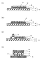
반도체 장치의 제조 방법은, 다이싱 테이프 일체형의 반도체 가공용 테이프(10) 상에 반도체 웨이퍼(W)를 접착하는 공정(마운트 공정)과, 반도체 웨이퍼(W)를 다이싱해서 반도체 칩(C)을 형성하는 공정(다이싱 공정)과, 반도체 칩(C)을 반도체 가공용 테이프(10)와 함께, 다이싱 테이프(13)의 점착제층(12)으로부터 박리하는 공정(픽업 공정)과, 반도체 칩(C)을 피 착체(16) 상에 플립 칩 접속하는 공정(플립 칩 접속 공정)을 적어도 구비한다.A method of manufacturing a semiconductor device includes a step of mounting a semiconductor wafer W on a
[마운트 공정][Mounting process]
우선, 다이싱 테이프 일체형의 반도체 가공용 테이프(10) 상에 임의로 설치된 세퍼레이터를 적절하게 박리하여, 도 2의 (A)에서 나타낸 바와 같이, 접착제층(15)에 반도체 웨이퍼(W)를 접착하고, 이것을 접착 유지시켜 고정한다(마운트 공정). 이때 접착제층(15)은, 미경화 상태(반경화 상태를 포함함)에 있다. 또한, 다이싱 테이프 일체형의 반도체 가공용 테이프(10)는, 반도체 웨이퍼(W)의 이면에 접착된다. 반도체 웨이퍼(W)의 이면이란, 회로면과는 반대측의 면(비회로면, 비전극 형성면 등으로도 불림)을 의미한다. 접착 방법은 특별히 한정되지 않지만, 가열 압착에 의한 방법이 바람직하다. 압착은, 통상 압착 롤 등의 가압 수단에 의해 가압하면서 행하여진다. 또한, 가열은 히트 스테이지를 접합 대로 하거나, 가열 압착 롤을 사용함으로써 행하여진다.A semiconductor wafer W is bonded to the
[다이싱 공정][Dicing process]
이어서, 도 2의 (B)에서 나타낸 바와 같이, 반도체 웨이퍼(W)의 다이싱을 행한다. 이에 의해, 반도체 웨이퍼(W)를 소정의 크기로 절단해서 개편화(소편화)하여, 반도체 칩(C)을 제조한다. 다이싱은, 예를 들어 반도체 웨이퍼(W)의 회로면측에서 통상법에 따라 행하여진다. 또한, 본 공정에서는, 예를 들어 반도체 가공용 테이프(10)까지 절입을 행하는 풀컷이라고 불리는 절단 방식 등을 채용할 수 있다. 본 공정에서 사용하는 다이싱 장치로서는 특별히 한정되지 않고, 종래 공지된 것을 사용할 수 있다. 또한, 반도체 웨이퍼(W)는, 반도체 가공용 테이프(10)에 의해 우수한 밀착성으로 접착 고정되어 있으므로, 칩 결함이나 칩 비산을 억제할 수 있음과 함께, 반도체 웨이퍼(W)의 파손도 억제할 수 있다. 또한, 다이싱 테이프 일체형의 반도체 가공용 테이프(10)의 익스팬드를 행하는 경우, 해당 익스팬드는 종래 공지된 익스팬드 장치를 사용해서 행할 수 있다.Subsequently, as shown in Fig. 2B, the semiconductor wafer W is diced. As a result, the semiconductor wafer W is cut to a predetermined size and fragmented to form a semiconductor chip (C). The dicing is performed, for example, in accordance with a conventional method on the circuit surface side of the semiconductor wafer W. Further, in this step, for example, a cutting method called a full cutting which infeeds up to the
[픽업 공정][Pick-up process]
도 2의 (C)에서 나타낸 바와 같이, 반도체 칩(C)의 픽업을 행하여, 반도체 칩(C)을 접착제층(15) 및 금속층(14)과 함께 다이싱 테이프(13)로부터 박리시킨다. 픽업의 방법으로서는 특별히 한정되지 않고, 종래 공지된 다양한 방법을 채용할 수 있다. 예를 들어, 개개의 반도체 칩(C)을 반도체 가공용 테이프(10)의 기재 필름(11)측으로부터 니들에 의해 밀어올리고, 밀어올려진 반도체 칩(C)을 픽업 장치에 의해 픽업하는 방법 등을 들 수 있다. 또한, 픽업된 반도체 칩(C)은, 그 이면이 금속층(14)에 의해 보호되어 있다.The semiconductor chip C is picked up and separated from the dicing
[플립 칩 접속 공정][Flip chip connecting step]
픽업한 반도체 칩(C)은, 도 2의 (D)에서 나타낸 바와 같이, 기판 등의 피 착체(16)에, 플립 칩 본딩 방식(플립 칩 실장 방식)에 의해 고정시킨다. 구체적으로는, 반도체 칩(C)을, 반도체 칩(C)의 회로면(표면, 회로 패턴 형성면, 전극 형성면 등으로도 불림)이 피 착체(16)와 대향하는 형태로, 피 착체(16)에 통상법에 따라 고정시킨다. 예를 들어, 먼저 반도체 칩(C)의 회로면측에 형성되어 있는 접속부로서의 범프(17)에 플럭스를 부착시킨다. 계속해서, 반도체 칩(C)의 범프(17)를 피 착체(16)의 접속 패드에 피착된 접합용 도전재(18)(땜납 등)에 접촉시켜 가압하면서 범프(17) 및 도전재(18)를 용융시킴으로써, 반도체 칩(C)과 피 착체(16)와의 전기적 도통을 확보하여, 반도체 칩(C)을 피 착체(16)에 고정시킬 수 있다(플립 칩 본딩 공정). 이때, 반도체 칩(C)과 피 착체(16)와의 사이에는 공극이 형성되어 있고, 그 공극간 거리는, 일반적으로 30㎛ 내지 300㎛ 정도이다. 또한, 반도체 칩(C)을 피 착체(16) 상에 플립 칩 본딩(플립 칩 접속)한 후에는, 반도체 칩(C)과 피 착체(16)와의 대향면이나 간극에 잔존하는 플럭스를 세정 제거하고, 해당 간극에 밀봉재(밀봉 수지 등)를 충전시켜서 밀봉한다.The picked up semiconductor chip C is fixed to an
피 착체(16)로서는, 리드 프레임이나 회로 기판(배선 회로 기판 등) 등의 각종 기판을 사용할 수 있다. 이러한 기판의 재질로서는, 특별히 한정되는 것은 아니지만, 세라믹 기판이나, 플라스틱 기판을 들 수 있다. 플라스틱 기판으로서는, 예를 들어 에폭시 기판, 비스말레이미드트리아진 기판, 폴리이미드 기판 등을 들 수 있다. 또한, 다른 반도체 칩을 피 착체(16)로 하고, 상기 반도체 칩(C)을 플립 칩 접속함으로써, 칩 온 칩 구조로 할 수도 있다.As the
<실시예><Examples>
이어서, 본 발명의 효과를 더욱 명확하게 하기 위해, 실시예 및 비교예에 대해서 상세하게 설명하는데, 본 발명은 이들 실시예에 한정되는 것은 아니다.Next, in order to further clarify the effects of the present invention, examples and comparative examples will be described in detail, but the present invention is not limited to these examples.
(1) 다이싱 테이프의 제작(1) Fabrication of dicing tape
(점착제층 조성물의 조정)(Adjustment of the pressure-sensitive adhesive layer composition)
관능기를 갖는 아크릴계 공중합체(A1)로서, 2-에틸헥실아크릴레이트, 2-히드록시에틸아크릴레이트 및 메타크릴산을 포함하고, 2-에틸헥실아크릴레이트의 비율이 60몰%, 질량 평균 분자량 70만의 공중합체를 제조하였다. 이어서, 요오드가가 20이 되도록, 2-이소시아네이토에틸메타크릴레이트를 첨가하고, 유리 전이 온도 -50℃, 수산기가 10mgKOH/g, 산가 5mgKOH/g의 아크릴계 공중합체(a-1)를 제조하였다.Ethylhexyl acrylate, 2-hydroxyethyl acrylate and methacrylic acid, wherein the ratio of 2-ethylhexyl acrylate is 60 mol%, the mass average molecular weight is 70 Were prepared. Then, 2-isocyanatoethyl methacrylate was added so that the iodine value was 20, and an acrylic copolymer (a-1) having a glass transition temperature of -50 ° C, a hydroxyl value of 10 mg KOH / g and an acid value of 5 mg KOH / .
아크릴계 공중합체(a-1) 100질량부에 대하여, 폴리이소시아네이트로서 코로네이트 L(상품명, 도소 가부시끼가이샤 제조)을 5질량부 첨가하고, 광중합 개시제로서 Esacure KIP 150(상품명, Lamberti사 제조)을 3질량부 첨가한 혼합물을, 아세트산에틸에 용해시키고, 교반해서 점착제 조성물을 제조하였다.5 parts by mass of Coronate L (trade name, manufactured by Toso Kabushiki Kaisha) as polyisocyanate was added to 100 parts by mass of the acrylic copolymer (a-1), Esacure KIP 150 (trade name, manufactured by Lamberti) was used as a photopolymerization initiator 3 parts by mass The resulting mixture was dissolved in ethyl acetate and stirred to prepare a pressure-sensitive adhesive composition.
기재 필름으로서 이하의 것을 제작하였다.The following were prepared as base films.
(기재 필름 1)(Base film 1)
폴리프로필렌 PP 및 열가소성 엘라스토머 HSBR의 혼합물(PP:HSBR=80:20)의 수지 비즈를 200℃에서 용융하고, 압출기를 사용해서 두께 100㎛의 긴 필름 형상으로 성형해서 기재 필름 1을 제작하였다. 폴리프로필렌 PP로서는, 이데미쯔 세끼유 가가꾸 가부시끼가이샤 제조의 F-300SP(상품명)를, 열가소성 엘라스토머 HSBR로서는, JSR가부시끼가이샤 제조의 다이나론 1320P(상품명)를 사용하였다.Resin beads of a mixture of polypropylene PP and thermoplastic elastomer HSBR (PP: HSBR = 80: 20) were melted at 200 占 폚 and molded into a long film of 100 占 퐉 thick using an extruder to prepare a
(기재 필름 2)(Base film 2)
에틸렌-아크릴산 공중합체 아이오노머의 수지 비즈를 200℃에서 용융하고, 압출기를 사용해서 두께 150㎛의 긴 필름 형상으로 성형해서 기재 필름 2를 제작하였다. 에틸렌-아크릴산 공중합체 아이오노머는, 미츠이 듀퐁 폴리케미컬 가부시끼가이샤 제조의 하이 밀란 1706(상품명)을 사용하였다.The resin beads of the ethylene-acrylic acid copolymer ionomer were melted at 200 占 폚 and molded into an elongated film having a thickness of 150 占 퐉 by using an extruder to prepare a base film 2. As the ethylene-acrylic acid copolymer ionomer, HYMILAN 1706 (trade name) manufactured by Mitsui DuPont Polychemicals Co., Ltd. was used.
(기재 필름 3)(Base film 3)
에틸렌-아크릴산 공중합체 아이오노머의 수지 비즈를 200℃에서 용융하고, 압출기를 사용해서 두께 100㎛의 긴 필름 형상으로 성형해서 기재 필름 3을 제작하였다. 에틸렌-아크릴산 공중합체 아이오노머는, 미츠이 듀퐁 폴리케미컬 가부시끼가이샤 제조의 하이 밀란 1601(상품명)을 사용하였다.The resin beads of the ethylene-acrylic acid copolymer ionomer were melted at 200 占 폚 and molded into an elongated film having a thickness of 100 占 퐉 by using an extruder to prepare a base film 3. As the ethylene-acrylic acid copolymer ionomer, HYMILLAN 1601 (trade name) manufactured by Mitsui DuPont Polychemicals Co., Ltd. was used.
(기재 필름 4)(Base film 4)
에틸렌-아크릴산 공중합체 아이오노머의 수지 비즈를 200℃에서 용융하고, 압출기를 사용해서 두께 100㎛의 긴 필름 형상으로 성형해서 기재 필름 4를 제작하였다. 에틸렌-아크릴산 공중합체 아이오노머는, 미츠이 듀퐁 폴리케미컬 가부시끼가이샤 제조의 하이 밀란 1855(상품명)를 사용하였다.The resin beads of the ethylene-acrylic acid copolymer ionomer were melted at 200 占 폚 and molded into a long film having a thickness of 100 占 퐉 by using an extruder to prepare a base film 4. As the ethylene-acrylic acid copolymer ionomer, HYMILAN 1855 (trade name) manufactured by Mitsui DuPont Polychemicals Co., Ltd. was used.
(기재 필름 5)(Base film 5)
에틸렌-메타크릴산 공중합체의 수지 비즈를 200℃에서 용융하고, 압출기를 사용해서 두께 100㎛의 긴 필름 형상으로 성형해서 기재 필름 5를 제작하였다. 에틸렌-메타크릴산 공중합체는, 미츠이 듀퐁 폴리케미컬 가부시끼가이샤 제조의 뉴크렐 NO35C(상품명)를 사용하였다.The resin beads of the ethylene-methacrylic acid copolymer were melted at 200 占 폚 and molded into a long film having a thickness of 100 占 퐉 by using an extruder to prepare a base film 5. As the ethylene-methacrylic acid copolymer, Newcrel NO35C (trade name) manufactured by Mitsui DuPont Polychemicals Co., Ltd. was used.
(기재 필름 6)(Base film 6)
폴리에틸렌테레프탈레이트의 수지 비즈를 280℃에서 용융하고, 압출기를 사용해서 두께 100㎛의 긴 필름 형상으로 성형해서 기재 필름 6을 제작하였다. 폴리에틸렌테레프탈레이트는, 도요 보세끼 가부시끼가이샤 제조의 코스모샤인 A4100(상품명)을 사용하였다.The resin beads of polyethylene terephthalate were melted at 280 占 폚 and molded into a long film having a thickness of 100 占 퐉 by using an extruder to prepare a base film 6. As the polyethylene terephthalate, COSMO SHINE A4100 (trade name) manufactured by Toyo Boseki Kabushiki Kaisha was used.
<다이싱 테이프(1)>≪ Dicing tape (1) >
이형 처리한 폴리에틸렌-테레프탈레이트 필름을 포함하는 박리 라이너에, 상기 점착제 조성물을, 건조 후의 두께가 10㎛가 되도록 도포 시공하고, 110℃에서 3분간 건조시킨 후, 상기 기재 필름 1과 접합하여, 다이싱 테이프(1)를 제작하였다.The pressure-sensitive adhesive composition was applied to a release liner including a release-treated polyethylene terephthalate film so that the thickness after drying was 10 占 퐉, dried at 110 占 폚 for 3 minutes and then bonded to the
<다이싱 테이프(2)>≪ Dicing tape (2) >
상기 기재 필름 2를 사용한 것 이외는 다이싱 테이프(1)와 마찬가지로 하여, 다이싱 테이프(2)를 제작하였다.A dicing tape 2 was produced in the same manner as the dicing
<다이싱 테이프(3)>≪ Dicing tape (3) >
상기 기재 필름 3을 사용한 것 이외는 다이싱 테이프(1)와 마찬가지로 하여, 다이싱 테이프(3)를 제작하였다.A dicing tape 3 was produced in the same manner as the dicing
<다이싱 테이프(4)>≪ Dicing tape (4) >
상기 기재 필름 4를 사용한 것 이외는 다이싱 테이프(1)와 마찬가지로 하여, 다이싱 테이프(4)를 제작하였다.A dicing tape 4 was produced in the same manner as the dicing
<다이싱 테이프(5)>≪ Dicing tape (5) >
상기 기재 필름 5를 사용한 것 이외는 다이싱 테이프(1)와 마찬가지로 하여, 다이싱 테이프(5)를 제작하였다.A dicing tape 5 was prepared in the same manner as the dicing
<다이싱 테이프(6)>≪ Dicing tape (6) >
상기 기재 필름 6을 사용한 것 이외는 다이싱 테이프(1)와 마찬가지로 하여, 다이싱 테이프(6)를 제작하였다.A dicing tape 6 was produced in the same manner as the dicing
(2) 접착제층의 제작(2) Production of adhesive layer
<접착제층(1)>≪ Adhesive Layer (1) >
에폭시 수지로서 「1002」(상품명, 미쯔비시 가가꾸 가부시끼가이샤 제조, 고형 비스페놀 A형 에폭시 수지, 에폭시 당량 600) 40질량부, 에폭시 수지로서 「806」(상품명, 미쯔비시 가가꾸 가부시끼가이샤 제조, 비스페놀 F형 에폭시 수지, 에폭시 당량 160, 비중 1.20) 100질량부, 경화제로서 「Dyhard100SF」(상품명, Degussa사, 디시안디아미드) 5질량부, 실리카 필러로서 「SO-C2」(상품명, 애드마파인 가부시끼가이샤 제조, 평균 입경 0.5㎛) 350질량부, 및 실리카 필러로서 「에어로실 R972」(상품명, 닛본에어로실 가부시끼가이샤 제조, 1차 입경의 평균 입경 0.016㎛) 3질량부를 포함하는 조성물에 메틸에틸케톤을 첨가하고, 교반 혼합하여, 균일한 조성물로 하였다., 40 parts by mass of epoxy resin "1002" (trade name, solid bisphenol A type epoxy resin, product of Mitsubishi Chemical Corporation, epoxy equivalent: 600), 806 parts by mass of epoxy resin (trade name: bisphenol, manufactured by Mitsubishi Chemical Corporation, 5 parts by mass of "Dyhard 100SF" (trade name, Degussa, dicyandiamide) as a curing agent, "SO-C2" as a silica filler (trade name, Admaffinity Appearance Ltd.) and 3 parts by mass of "Aerosil R972" (trade name, manufactured by Nippon Aerosil Co., Ltd., average particle diameter of primary particle size: 0.016 μm) as silica filler were added to a composition of methyl Ethyl ketone was added thereto, followed by stirring and mixing to obtain a homogeneous composition.
이것에, 페녹시 수지로서 「PKHH」(상품명, INCHEM사 제조, 질량 평균 분자량 52,000, 유리 전이 온도 92℃) 100질량부, 커플링제로서 「KBM-802」(상품명, 신에쓰 실리콘 가부시끼가이샤 제조, 머캅토프로필트리메톡시실란) 0.6질량부, 및 경화 촉진제로서 「큐어졸 2PHZ-PW」(상품명, 시꼬꾸 가세 가부시끼가이샤 제조, 2-페닐-4,5-디히드록시메틸이미다졸, 분해 온도 230℃) 0.5질량부를 첨가하여, 균일해질 때까지 교반 혼합하였다. 또한 이것을 100 메쉬의 필터로 여과하고, 진공 탈포함으로써, 접착제 조성물 b-1의 바니시를 얻었다.100 parts by mass of "PKHH" (trade name, manufactured by INCHEM, mass average molecular weight: 52,000, glass transition temperature: 92 ° C.) as a phenoxy resin, "KBM-802" (trade name, manufactured by Shinetsu Silicones Co., , 0.6 part by mass of mercaptopropyltrimethoxysilane), and 0.6 part by mass of "Curezol 2PHZ-PW" (trade name, available from Shikoku Chemical Industries, Ltd., 2-phenyl-4,5-dihydroxymethylimidazole , Decomposition temperature 230 deg. C), and the mixture was stirred and mixed until homogeneous. This was further filtered through a 100-mesh filter and vacuum degassed to obtain a varnish of the adhesive composition b-1.
이형 처리한 폴리에틸렌-테레프탈레이트 필름을 포함하는 세퍼레이터에, 접착제 조성물 b-1을, 건조 후의 두께가 8㎛가 되도록 도포 시공하고, 110℃에서 5분간 건조시켜, 세퍼레이터 상에 접착제층(1)이 형성된 접착 필름을 제작하였다.The adhesive composition b-1 was applied to a separator including a polyethylene terephthalate film subjected to releasing treatment so that the thickness after drying became 8 占 퐉 and dried at 110 占 폚 for 5 minutes to form an
(3) 금속층(3)
금속층으로서 이하의 것을 준비하였다.The following metal layers were prepared.
<금속층(1)>≪ Metal layer (1) >
1085(상품명, 도요알루미늄 가부시끼가이샤 제조, 알루미늄박, 두께 12㎛, 열전도율 221W/m·K)1085 (trade name, aluminum foil,
<금속층(2)>≪ Metal layer (2) >
압연 구리박(상품명, 가부시키가이샤 UACJ 제조, 터프 피치 구리박, 두께 18㎛, 열전도율 391W/m·K)Rolled copper foil (trade name, manufactured by UACJ, tough pitch copper foil,
<금속층(3)>≪ Metal layer (3) >
C18040(상품명, 가부시키가이샤 UACJ 제조, 구리 합금 박, 두께 18㎛, 열전도율 322W/m·K)C18040 (trade name, copper alloy foil,
<금속층(4)>≪ Metal layer (4) >
SUS304(상품명, 신닛테츠스미킨 머티리얼즈 가부시끼가이샤 제조, 스테인리스박, 두께 20㎛, 열전도율 16.3W/m·K)SUS304 (trade name, a stainless steel foil, thickness 20 占 퐉, thermal conductivity 16.3 W / m 占 K, manufactured by Shinnitetsu Semiconductor Materials Co., Ltd.)
(4) 반도체 가공용 테이프의 제작(4) Fabrication of tape for semiconductor processing
<실시예 1>≪ Example 1 >
이상과 같이 해서 얻어진 접착제층(1)과 금속층(1)을 접합해서 각도 120°, 압력 0.2MPa, 속도 10mm/s의 조건에서 접합 편면 접착 필름을 제작하였다. 다이싱 테이프(1)를 링 프레임에 접합할 수 있는 형상으로, 편면 접착 필름을 웨이퍼를 덮을 수 있는 형상으로 프리컷하고, 상기 다이싱 테이프(1)의 점착제층과 상기 편면 접착 필름의 금속층측을, 편면 접착 필름의 주위에 점착제층이 노출되도록 접합하여, 실시예 1의 반도체 가공용 테이프를 제작하였다.The
<실시예 2 내지 7, 비교예 1 내지 3>≪ Examples 2 to 7 and Comparative Examples 1 to 3 >
다이싱 테이프, 접착제 조성물, 금속층의 조합을 표 1에 기재된 조합으로 한 것 이외는, 실시예 1과 마찬가지의 방법에 의해, 실시예 2 내지 7, 비교예 1 내지 3의 반도체 가공용 테이프를 제작하였다.The tape for semiconductor processing of Examples 2 to 7 and Comparative Examples 1 to 3 was produced in the same manner as in Example 1 except that the combination of the dicing tape, the adhesive composition and the metal layer was used in combination as shown in Table 1 .
실시예 1 내지 7 및 비교예 1 내지 3에 관한 반도체 가공용 테이프에 대해서 이하의 측정 및 평가를 행하였다. 그 결과를 표 1에 나타내었다.The following measurements and evaluations were conducted on the semiconductor processing tapes according to Examples 1 to 7 and Comparative Examples 1 to 3. The results are shown in Table 1.
(루프 스티프니스의 측정)(Measurement of loop stiffness)
각 실시예, 비교예에 사용한 다이싱 테이프에 대해서, 이하의 조건에 의해 루프 스티프니스를 측정하였다. 측정 결과를 표 1에 나타내었다.For each of the dicing tapes used in the examples and comparative examples, the loop stiffness was measured under the following conditions. The measurement results are shown in Table 1.
루프 스티프니스 측정 조건:Loop Stiffness Measurement conditions:
장치; 루프 스티프니스 테스터 DA(도요 세끼 가부시끼가이샤 제조, 상품명)Device; Loop Stiffness Tester DA (trade name, manufactured by TOYO SEKI KABUSHIKI KAISHA)
루프(샘플)형상; 길이 80mm, 폭 25mmLoop (sample) shape; Length 80mm, width 25mm
압자의 압입 속도; 3.3mm/secIndentation speed of indenter; 3.3mm / sec
측정 데이터; 폭 25mm로 잘라낸 다이싱 테이프의 시험편을 점착제층이 부착되어 있는 표면이 루프의 내측이 되도록 Ω자 형상의 루프형으로 구부린 다음, 그 길이 방향의 양단을 겹쳐서, 루프의 둘레 길이가 80mm가 되도록 그 겹친 부분을 척으로 파지하였다. 시험편을 루프가 환 형상이 되도록 고정하고, 그 루프를 압축 속도 3.3mm/sec으로, 압자가 루프와 접촉한 시점에서부터 10mm 압입했을 때 로드셀에 검출되는 부하 하중값을 구함으로써 측정한다.Measurement data; A test piece of a dicing tape cut into a width of 25 mm was bent into a loop shape having an Ω shape so that the surface with the adhesive layer on the inner side of the loop was overlapped and both ends in the longitudinal direction thereof were overlapped, The overlapped portion was gripped with a chuck. The test piece is fixed to the loop so that the loop is annular and the loop is measured at a compression rate of 3.3 mm / sec by calculating the load load value detected on the load cell when the indenter is pressed 10 mm from the point of contact with the loop.
(라미네이트성의 평가)(Evaluation of lamination property)
각 실시예, 비교예에 관한 반도체 가공용 테이프를, 이하의 조건에 의해 반도체 웨이퍼 10매에 접합하였다. 반도체 웨이퍼에 접합된 반도체 가공용 테이프를 관찰하여, 조건 1, 2의 양쪽에서 1매도 금속층에 주름이 발생하지 않고 접합할 수 있었던 것을 우량품으로서 ◎, 조건 1에서는 금속층에 주름이 발생했지만, 조건 2에서는 1매도 금속층에 주름이 발생하지 않고 접합할 수 있었던 것을 양품으로서 ○, 조건 1, 2의 양쪽에서 1매라도 금속층에 주름이 발생한 것을 불량품으로서 ×로 평가하였다. 평가 결과를 표 1에 나타내었다.The semiconductor processing tapes according to each of the examples and comparative examples were bonded to 10 semiconductor wafers under the following conditions. The tape for semiconductor processing bonded to a semiconductor wafer was observed, and it was found that the metal layer could be joined without causing any wrinkles in both of the
<라미네이트 조건 1>≪
라미네이트 장치: 웨이퍼 마운터 DAM-812M(가부시키가이샤 타카토리 제조, 상품명)Lamination apparatus: wafer mounter DAM-812M (trade name, manufactured by Takatori Kogyo Co., Ltd.)
라미네이트 속도: 30mm/secLamination speed: 30mm / sec
라미네이트 압력: 0.1MPaLaminate pressure: 0.1 MPa
라미네이트 온도: 90℃Laminate temperature: 90 ° C
<라미네이트 조건 2>≪ Lamination condition 2 >
라미네이트 장치: 웨이퍼 마운터 DAM-812M(가부시키가이샤 타카토리 제조, 상품명)Lamination apparatus: wafer mounter DAM-812M (trade name, manufactured by Takatori Kogyo Co., Ltd.)
라미네이트 속도: 10mm/secLamination speed: 10mm / sec
라미네이트 압력: 0.1MPaLaminate pressure: 0.1 MPa
라미네이트 온도: 90℃Laminate temperature: 90 ° C
(픽업성의 평가)(Evaluation of pickupability)
각 실시예, 비교예에 관한 반도체 가공용 테이프에 접합한 반도체 웨이퍼를, 다이싱 장치로서 DAD340(가부시키가이샤 디스코 제조, 상품명)을 사용해서 설정한 분할 예정 라인을 따라 15×8mm 사각으로 풀컷하였다. 다이싱 테이프의 기재 필름측으로부터, 자외선을 200mJ/mm2 조사해서 점착제층을 경화시킨 후, 개편화한 반도체 칩을, 다이스 피커 장치로서 CAP-300II(캐논 머시너리 가부시끼가이샤 제조)를 사용해서 픽업하였다. 핀 하이트의 설정은 400㎛로 하였다. 100개의 반도체 칩을 픽업하여, 95개 이상 문제없이 픽업할 수 있었던 것을 양품으로서 ○, 95개 미만밖에 픽업할 수 없었던 것을 불량품으로서 ×로 평가하였다. 또한, 비교예 1 및 비교예 3은, 반도체 웨이퍼에 양호하게 접합할 수 없었기 때문에, 픽업 시험은 실시하지 않았다.The semiconductor wafer bonded to the semiconductor processing tape according to each of the examples and the comparative examples was cut in a 15 × 8 mm square along a line to be divided set using DAD 340 (trade name, manufactured by DISCO Corporation) as a dicing machine. After the pressure-sensitive adhesive layer was cured by irradiating ultraviolet rays of 200 mJ / mm 2 from the base film side of the dicing tape, individual semiconductor chips were dipped in a die picker apparatus using CAP-300II (manufactured by Canon Machinery Co., Ltd.) Picked up. The setting of the pin height was 400 mu m. 100 semiconductor chips were picked up, and those that could be picked up with no more than 95 problems were evaluated as good, and those that could not be picked up less than 95 were evaluated as poor. In addition, since Comparative Example 1 and Comparative Example 3 could not be satisfactorily bonded to a semiconductor wafer, no pick-up test was conducted.
<레이저 마크성의 평가><Evaluation of laser markability>
픽업성의 평가에서 얻어진 반도체 칩에 대해서, 이하의 조건에 의해 문자 가공을 행하였다. 이하의 평가 기준에 의해 평가하였다. 레이저 마킹에 의해 형성된 문자가 육안(육안 거리: 약 30cm)으로 시인할 수 있었던 것을 양품으로서 ○, 시인할 수 없었던 것을 불량품으로서 ×로 평가하였다.The semiconductor chip obtained in the evaluation of pickupability was subjected to character processing under the following conditions. And evaluated according to the following evaluation criteria. The characters formed by the laser marking were visually observed with naked eyes (visual distance: about 30 cm), and those which were not recognized as good were evaluated as poor.
<레이저 마킹 조건>≪ Laser Marking Condition >
레이저 마킹 장치: MD-X1000(가부시키가이샤 키엔스 제조, 상품명)Laser marking apparatus: MD-X1000 (trade name, manufactured by KABUSHIKI KAISHA)
파장: 1064nmWavelength: 1064 nm
강도: 13WStrength: 13W
스캔 스피드: 500mm/secScan speed: 500mm / sec
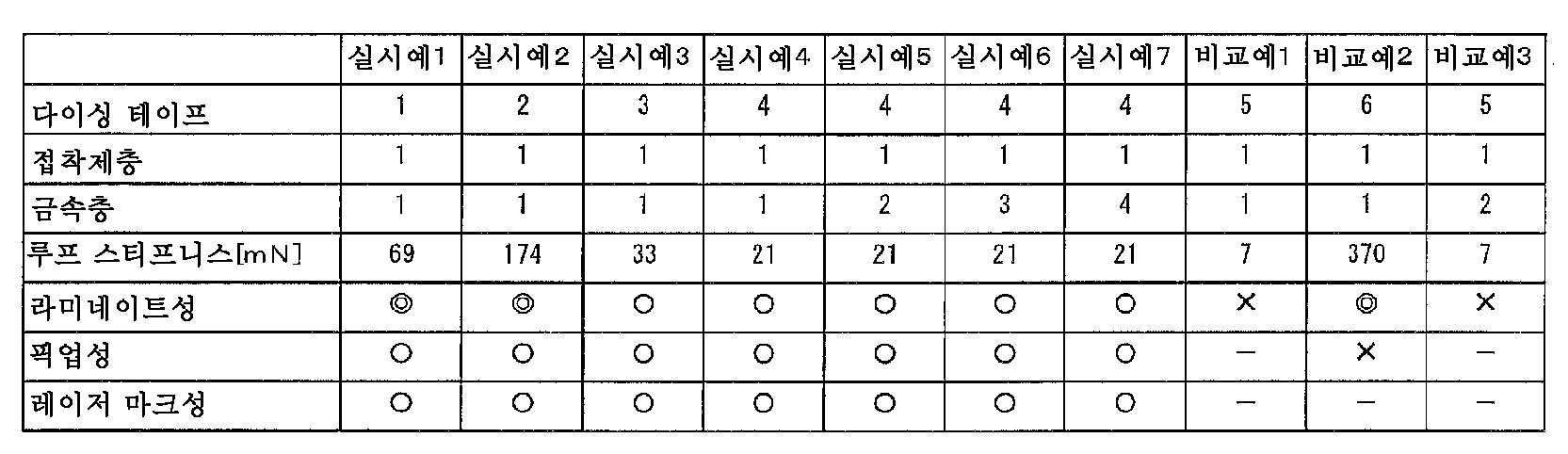
표 1에 나타낸 바와 같이, 실시예 1 내지 7에 관한 반도체 가공용 테이프는, 다이싱 테이프의 루프 스티프니스가 21mN 이상 174mN 이하로, 청구항에 규정하는 20mN 이상 200mN 미만이기 때문에, 라미네이트성, 픽업성 모두 양호한 결과가 되었다.As shown in Table 1, in the semiconductor processing tapes according to Examples 1 to 7, since the loop stiffness of the dicing tape is 21 mN or more and 174 mN or less and 20 mN or more and 200 mN or less as defined in the claims, Results.
이에 반해, 비교예 1 및 3에 관한 반도체 가공용 테이프는, 다이싱 테이프의 루프 스티프니스가 20mN 미만이기 때문에, 라미네이트성이 떨어지는 결과가 되었다. 또한, 비교예 2에 관한 반도체 가공용 테이프는, 다이싱 테이프의 루프 스티프니스가 200mN 이상이기 때문에, 픽업성이 떨어지는 결과가 되었다.On the contrary, in the semiconductor processing tapes according to Comparative Examples 1 and 3, since the loop stiffness of the dicing tape was less than 20 mN, the lamination property was deteriorated. In the semiconductor processing tape according to Comparative Example 2, since the loop stiffness of the dicing tape was 200 mN or more, the pickup property was deteriorated.
10: 반도체 가공용 테이프
11: 기재 필름
12: 점착제층
13: 다이싱 테이프
14: 금속층
15: 접착제층10: tape for semiconductor processing 11: substrate film
12: pressure-sensitive adhesive layer 13: dicing tape
14: metal layer 15: adhesive layer
Claims (3)
상기 점착제층 상에 설치된 금속층과,
상기 금속층 상에 설치되어 있고, 상기 금속층을 반도체 칩의 이면에 접착하기 위한 접착제층을 갖고,
상기 다이싱 테이프의 루프 스티프니스가 20mN 이상 200mN 미만인 것을 특징으로 하는 반도체 가공용 테이프.A dicing tape having a base film and a pressure-sensitive adhesive layer,
A metal layer provided on the pressure-sensitive adhesive layer,
An adhesive layer provided on the metal layer for adhering the metal layer to the back surface of the semiconductor chip,
Wherein the dicing tape has a loop stiffness of 20 mN or more and less than 200 mN.
상기 금속층이 알루미늄, 철, 티타늄, 주석, 니켈 및 구리로 이루어지는 군에서 선택되는 적어도 1종의 금속 및/또는 그들의 합금 중 어느 하나를 포함하는 것을 특징으로 하는, 반도체 가공용 테이프.The method according to claim 1,
Wherein the metal layer comprises any one of at least one metal selected from the group consisting of aluminum, iron, titanium, tin, nickel and copper and / or alloys thereof.
상기 다이싱 테이프의 두께가, 55㎛ 이상 215㎛ 미만인 것을 특징으로 하는, 반도체 가공용 테이프.3. The method according to claim 1 or 2,
Wherein the thickness of the dicing tape is not less than 55 占 퐉 and less than 215 占 퐉.
Applications Claiming Priority (3)
| Application Number | Priority Date | Filing Date | Title |
|---|---|---|---|
| JP2015255313 | 2015-12-25 | ||
| JPJP-P-2015-255313 | 2015-12-25 | ||
| PCT/JP2016/079627 WO2017110203A1 (en) | 2015-12-25 | 2016-10-05 | Tape for semiconductor processing |
Publications (2)
| Publication Number | Publication Date |
|---|---|
| KR20180098125A true KR20180098125A (en) | 2018-09-03 |
| KR102513252B1 KR102513252B1 (en) | 2023-03-24 |
Family
ID=59089994
Family Applications (1)
| Application Number | Title | Priority Date | Filing Date |
|---|---|---|---|
| KR1020177031446A Active KR102513252B1 (en) | 2015-12-25 | 2016-10-05 | Tape for semiconductor processing |
Country Status (7)
| Country | Link |
|---|---|
| JP (1) | JP6800167B2 (en) |
| KR (1) | KR102513252B1 (en) |
| CN (1) | CN107960133B (en) |
| MY (1) | MY192250A (en) |
| SG (1) | SG11201708735SA (en) |
| TW (1) | TWI696683B (en) |
| WO (1) | WO2017110203A1 (en) |
Families Citing this family (13)
| Publication number | Priority date | Publication date | Assignee | Title |
|---|---|---|---|---|
| TWI649398B (en) * | 2017-09-11 | 2019-02-01 | 達邁科技股份有限公司 | Thermal-curable adhesive composition and adhesive sheet |
| US10947417B2 (en) | 2017-09-29 | 2021-03-16 | Taimide Tech. Inc. | Thermal-curable adhesive composition and adhesive sheet |
| JP7154809B2 (en) * | 2018-04-20 | 2022-10-18 | 株式会社ディスコ | Wafer processing method |
| JP7111562B2 (en) * | 2018-08-31 | 2022-08-02 | 株式会社ディスコ | Processing method |
| US11541691B2 (en) | 2018-12-19 | 2023-01-03 | The Goodyear Tire & Rubber Company | Composite tread with targeted stiffness gradient and method of making |
| US11993110B2 (en) | 2018-12-19 | 2024-05-28 | The Goodyear Tire & Rubber Company | Reinforced tread and method of forming |
| US20200198414A1 (en) * | 2018-12-19 | 2020-06-25 | The Goodyear Tire & Rubber Company | Method and apparatus for forming a composite tread with microchimneys |
| JP7321639B2 (en) * | 2019-02-15 | 2023-08-07 | 株式会社ディスコ | Wafer processing method |
| JP7258421B2 (en) * | 2019-02-15 | 2023-04-17 | 株式会社ディスコ | Wafer processing method |
| JP7379829B2 (en) * | 2019-02-21 | 2023-11-15 | 味の素株式会社 | Manufacturing method of printed wiring board |
| CN114097073B (en) * | 2019-11-28 | 2025-12-23 | 积水化学工业株式会社 | Method for manufacturing semiconductor devices and laminates for semiconductor processing |
| TWI710288B (en) * | 2020-01-22 | 2020-11-11 | 頎邦科技股份有限公司 | Method and device for adhering heat sinks to a circuit board tape |
| TWI887672B (en) * | 2023-06-06 | 2025-06-21 | 萬潤科技股份有限公司 | Laminating method, laminating module, laminating device and laminating equipment |
Citations (5)
| Publication number | Priority date | Publication date | Assignee | Title |
|---|---|---|---|---|
| JPH1167699A (en) * | 1997-08-13 | 1999-03-09 | Texas Instr Japan Ltd | Method for manufacturing semiconductor device |
| JP2007158026A (en) | 2005-12-05 | 2007-06-21 | Furukawa Electric Co Ltd:The | Chip protection film forming sheet |
| JP2007235022A (en) | 2006-03-03 | 2007-09-13 | Mitsui Chemicals Inc | Adhesive film |
| JP2008235716A (en) * | 2007-03-22 | 2008-10-02 | Furukawa Electric Co Ltd:The | Adhesive tape for semiconductor device processing |
| JP2012033626A (en) | 2010-07-29 | 2012-02-16 | Nitto Denko Corp | Film for flip-chip type semiconductor rear face, and use thereof |
Family Cites Families (3)
| Publication number | Priority date | Publication date | Assignee | Title |
|---|---|---|---|---|
| JP4849993B2 (en) * | 2006-08-14 | 2012-01-11 | 日東電工株式会社 | Adhesive sheet, method for producing the same, and method for cutting laminated ceramic sheet |
| JP5534690B2 (en) * | 2009-03-23 | 2014-07-02 | 古河電気工業株式会社 | Dicing tape |
| JP5681374B2 (en) * | 2010-04-19 | 2015-03-04 | 日東電工株式会社 | Dicing tape integrated semiconductor backside film |
-
2016
- 2016-10-05 WO PCT/JP2016/079627 patent/WO2017110203A1/en not_active Ceased
- 2016-10-05 CN CN201680025557.8A patent/CN107960133B/en active Active
- 2016-10-05 KR KR1020177031446A patent/KR102513252B1/en active Active
- 2016-10-05 MY MYPI2017001596A patent/MY192250A/en unknown
- 2016-10-05 SG SG11201708735SA patent/SG11201708735SA/en unknown
- 2016-10-05 JP JP2017557751A patent/JP6800167B2/en active Active
- 2016-12-22 TW TW105142786A patent/TWI696683B/en active
Patent Citations (6)
| Publication number | Priority date | Publication date | Assignee | Title |
|---|---|---|---|---|
| JPH1167699A (en) * | 1997-08-13 | 1999-03-09 | Texas Instr Japan Ltd | Method for manufacturing semiconductor device |
| JP2007158026A (en) | 2005-12-05 | 2007-06-21 | Furukawa Electric Co Ltd:The | Chip protection film forming sheet |
| JP2007235022A (en) | 2006-03-03 | 2007-09-13 | Mitsui Chemicals Inc | Adhesive film |
| JP2008235716A (en) * | 2007-03-22 | 2008-10-02 | Furukawa Electric Co Ltd:The | Adhesive tape for semiconductor device processing |
| JP2012033626A (en) | 2010-07-29 | 2012-02-16 | Nitto Denko Corp | Film for flip-chip type semiconductor rear face, and use thereof |
| KR20150094581A (en) * | 2010-07-29 | 2015-08-19 | 닛토덴코 가부시키가이샤 | Film for flip chip type semiconductor back surface and its use |
Also Published As
| Publication number | Publication date |
|---|---|
| JP6800167B2 (en) | 2020-12-16 |
| JPWO2017110203A1 (en) | 2018-10-18 |
| KR102513252B1 (en) | 2023-03-24 |
| CN107960133A (en) | 2018-04-24 |
| TWI696683B (en) | 2020-06-21 |
| CN107960133B (en) | 2021-10-26 |
| TW201722711A (en) | 2017-07-01 |
| SG11201708735SA (en) | 2018-07-30 |
| MY192250A (en) | 2022-08-11 |
| WO2017110203A1 (en) | 2017-06-29 |
Similar Documents
| Publication | Publication Date | Title |
|---|---|---|
| KR102513252B1 (en) | Tape for semiconductor processing | |
| JP6422462B2 (en) | Electronic device packaging tape | |
| CN102399505B (en) | Dicing/die bonding film | |
| JP6310492B2 (en) | Electronic device packaging tape | |
| JP2009049400A (en) | Thermosetting die bond film | |
| CN104946150A (en) | Chip bonding film, chip bonding film with cutting sheet, semiconductor and making method thereof | |
| JP5696205B2 (en) | Die bond film, dicing die bond film and semiconductor device | |
| JP6852030B2 (en) | Electronic device packaging tape | |
| KR20180067522A (en) | Tape for electronic device package | |
| JP2011165716A (en) | Thermosetting die-bonding film, dicing die-bonding film, and semiconductor device | |
| KR20180064367A (en) | Electronic device package, method of manufacturing electronic device package, and tape for electronic device package | |
| JP2021185610A (en) | Tape for electronic device package | |
| KR102580602B1 (en) | Tape for semiconductor processing | |
| JP6339619B2 (en) | Electronic device packaging tape | |
| KR20180129789A (en) | Tape for electronic device package | |
| JP6655576B2 (en) | Electronic device packaging tape | |
| JP6440657B2 (en) | Tape for electronic devices | |
| JP2021072345A (en) | Electronic device package tape |
Legal Events
| Date | Code | Title | Description |
|---|---|---|---|
| PA0105 | International application |
St.27 status event code: A-0-1-A10-A15-nap-PA0105 |
|
| PG1501 | Laying open of application |
St.27 status event code: A-1-1-Q10-Q12-nap-PG1501 |
|
| P22-X000 | Classification modified |
St.27 status event code: A-2-2-P10-P22-nap-X000 |
|
| A201 | Request for examination | ||
| PA0201 | Request for examination |
St.27 status event code: A-1-2-D10-D11-exm-PA0201 |
|
| R18-X000 | Changes to party contact information recorded |
St.27 status event code: A-3-3-R10-R18-oth-X000 |
|
| E902 | Notification of reason for refusal | ||
| PE0902 | Notice of grounds for rejection |
St.27 status event code: A-1-2-D10-D21-exm-PE0902 |
|
| P11-X000 | Amendment of application requested |
St.27 status event code: A-2-2-P10-P11-nap-X000 |
|
| P13-X000 | Application amended |
St.27 status event code: A-2-2-P10-P13-nap-X000 |
|
| E90F | Notification of reason for final refusal | ||
| PE0902 | Notice of grounds for rejection |
St.27 status event code: A-1-2-D10-D21-exm-PE0902 |
|
| P11-X000 | Amendment of application requested |
St.27 status event code: A-2-2-P10-P11-nap-X000 |
|
| P13-X000 | Application amended |
St.27 status event code: A-2-2-P10-P13-nap-X000 |
|
| E701 | Decision to grant or registration of patent right | ||
| PE0701 | Decision of registration |
St.27 status event code: A-1-2-D10-D22-exm-PE0701 |
|
| GRNT | Written decision to grant | ||
| PR0701 | Registration of establishment |
St.27 status event code: A-2-4-F10-F11-exm-PR0701 |
|
| PR1002 | Payment of registration fee |
St.27 status event code: A-2-2-U10-U12-oth-PR1002 Fee payment year number: 1 |
|
| PG1601 | Publication of registration |
St.27 status event code: A-4-4-Q10-Q13-nap-PG1601 |
|
| P22-X000 | Classification modified |
St.27 status event code: A-4-4-P10-P22-nap-X000 |
|
| PR1001 | Payment of annual fee |
St.27 status event code: A-4-4-U10-U11-oth-PR1001 Fee payment year number: 4 |
|
| U11 | Full renewal or maintenance fee paid |
Free format text: ST27 STATUS EVENT CODE: A-4-4-U10-U11-OTH-PR1001 (AS PROVIDED BY THE NATIONAL OFFICE) Year of fee payment: 4 |