KR20180064509A - Optical ferrules with waveguide inaccessible space - Google Patents
Optical ferrules with waveguide inaccessible space Download PDFInfo
- Publication number
- KR20180064509A KR20180064509A KR1020187013156A KR20187013156A KR20180064509A KR 20180064509 A KR20180064509 A KR 20180064509A KR 1020187013156 A KR1020187013156 A KR 1020187013156A KR 20187013156 A KR20187013156 A KR 20187013156A KR 20180064509 A KR20180064509 A KR 20180064509A
- Authority
- KR
- South Korea
- Prior art keywords
- waveguide
- optical
- light
- groove
- input surface
- Prior art date
Links
Images


Classifications
-
- G—PHYSICS
- G02—OPTICS
- G02B—OPTICAL ELEMENTS, SYSTEMS OR APPARATUS
- G02B6/00—Light guides; Structural details of arrangements comprising light guides and other optical elements, e.g. couplings
- G02B6/24—Coupling light guides
- G02B6/36—Mechanical coupling means
- G02B6/38—Mechanical coupling means having fibre to fibre mating means
- G02B6/3807—Dismountable connectors, i.e. comprising plugs
- G02B6/3833—Details of mounting fibres in ferrules; Assembly methods; Manufacture
- G02B6/3834—Means for centering or aligning the light guide within the ferrule
- G02B6/3838—Means for centering or aligning the light guide within the ferrule using grooves for light guides
- G02B6/3839—Means for centering or aligning the light guide within the ferrule using grooves for light guides for a plurality of light guides
-
- G—PHYSICS
- G02—OPTICS
- G02B—OPTICAL ELEMENTS, SYSTEMS OR APPARATUS
- G02B6/00—Light guides; Structural details of arrangements comprising light guides and other optical elements, e.g. couplings
- G02B6/24—Coupling light guides
- G02B6/36—Mechanical coupling means
- G02B6/3628—Mechanical coupling means for mounting fibres to supporting carriers
- G02B6/3648—Supporting carriers of a microbench type, i.e. with micromachined additional mechanical structures
- G02B6/3652—Supporting carriers of a microbench type, i.e. with micromachined additional mechanical structures the additional structures being prepositioning mounting areas, allowing only movement in one dimension, e.g. grooves, trenches or vias in the microbench surface, i.e. self aligning supporting carriers
-
- G—PHYSICS
- G02—OPTICS
- G02B—OPTICAL ELEMENTS, SYSTEMS OR APPARATUS
- G02B6/00—Light guides; Structural details of arrangements comprising light guides and other optical elements, e.g. couplings
- G02B6/24—Coupling light guides
- G02B6/36—Mechanical coupling means
- G02B6/38—Mechanical coupling means having fibre to fibre mating means
- G02B6/3807—Dismountable connectors, i.e. comprising plugs
- G02B6/381—Dismountable connectors, i.e. comprising plugs of the ferrule type, e.g. fibre ends embedded in ferrules, connecting a pair of fibres
- G02B6/3818—Dismountable connectors, i.e. comprising plugs of the ferrule type, e.g. fibre ends embedded in ferrules, connecting a pair of fibres of a low-reflection-loss type
- G02B6/382—Dismountable connectors, i.e. comprising plugs of the ferrule type, e.g. fibre ends embedded in ferrules, connecting a pair of fibres of a low-reflection-loss type with index-matching medium between light guides
-
- G—PHYSICS
- G02—OPTICS
- G02B—OPTICAL ELEMENTS, SYSTEMS OR APPARATUS
- G02B6/00—Light guides; Structural details of arrangements comprising light guides and other optical elements, e.g. couplings
- G02B6/24—Coupling light guides
- G02B6/36—Mechanical coupling means
- G02B6/38—Mechanical coupling means having fibre to fibre mating means
- G02B6/3807—Dismountable connectors, i.e. comprising plugs
- G02B6/3833—Details of mounting fibres in ferrules; Assembly methods; Manufacture
- G02B6/3834—Means for centering or aligning the light guide within the ferrule
- G02B6/3838—Means for centering or aligning the light guide within the ferrule using grooves for light guides
-
- G—PHYSICS
- G02—OPTICS
- G02B—OPTICAL ELEMENTS, SYSTEMS OR APPARATUS
- G02B6/00—Light guides; Structural details of arrangements comprising light guides and other optical elements, e.g. couplings
- G02B6/24—Coupling light guides
- G02B6/36—Mechanical coupling means
- G02B6/38—Mechanical coupling means having fibre to fibre mating means
- G02B6/3807—Dismountable connectors, i.e. comprising plugs
- G02B6/3833—Details of mounting fibres in ferrules; Assembly methods; Manufacture
- G02B6/3853—Lens inside the ferrule
-
- G—PHYSICS
- G02—OPTICS
- G02B—OPTICAL ELEMENTS, SYSTEMS OR APPARATUS
- G02B6/00—Light guides; Structural details of arrangements comprising light guides and other optical elements, e.g. couplings
- G02B6/24—Coupling light guides
- G02B6/36—Mechanical coupling means
- G02B6/38—Mechanical coupling means having fibre to fibre mating means
- G02B6/3807—Dismountable connectors, i.e. comprising plugs
- G02B6/3833—Details of mounting fibres in ferrules; Assembly methods; Manufacture
- G02B6/3855—Details of mounting fibres in ferrules; Assembly methods; Manufacture characterised by the method of anchoring or fixing the fibre within the ferrule
- G02B6/3861—Adhesive bonding
-
- G—PHYSICS
- G02—OPTICS
- G02B—OPTICAL ELEMENTS, SYSTEMS OR APPARATUS
- G02B6/00—Light guides; Structural details of arrangements comprising light guides and other optical elements, e.g. couplings
- G02B6/24—Coupling light guides
- G02B6/36—Mechanical coupling means
- G02B6/38—Mechanical coupling means having fibre to fibre mating means
- G02B6/3807—Dismountable connectors, i.e. comprising plugs
- G02B6/3873—Connectors using guide surfaces for aligning ferrule ends, e.g. tubes, sleeves, V-grooves, rods, pins, balls
- G02B6/3885—Multicore or multichannel optical connectors, i.e. one single ferrule containing more than one fibre, e.g. ribbon type
Landscapes
- Physics & Mathematics (AREA)
- General Physics & Mathematics (AREA)
- Optics & Photonics (AREA)
- Chemical & Material Sciences (AREA)
- Crystallography & Structural Chemistry (AREA)
- Optical Couplings Of Light Guides (AREA)
- Mechanical Coupling Of Light Guides (AREA)
Abstract
광학 페룰은 광이 광학 페룰 내에서 전파될 때, 광 도파관으로부터의 광의 하나 이상의 특성들에 영향을 미치도록 구성된 적어도 하나의 광 영향 요소를 포함하며, 광 영향 요소는 입력 표면을 갖는다. 적어도 하나의 수용 요소는 도파관의 출력 표면이 광 영향 요소의 입력 표면에 광학적으로 결합되도록 광 도파관을 수용하고 그를 페룰에 고정한다. 도파관 정지부는 광 도파관이 수용 요소 내에 설치되는 경우에 광 영향 요소의 입력 표면을 향한 도파관의 이동을 제한한다. 광 도파관이 수용 요소 내에 설치되는 경우에, 광 도파관은 광 도파관의 출력 표면과 광 영향 요소의 입력 표면 사이의 공간에 접근불가능하다.The optical ferrule includes at least one light influencing element configured to affect one or more characteristics of light from the light pipe when the light propagates in the optical ferrule, the light influencing element having an input surface. At least one receiving element receives the optical waveguide and secures it to the ferrule such that the output surface of the waveguide is optically coupled to the input surface of the optical influencing element. The waveguide stop limits movement of the waveguide towards the input surface of the light influencing element when the optical waveguide is installed in the receiving element. When the optical waveguide is installed in the receiving element, the optical waveguide is inaccessible to the space between the output surface of the optical waveguide and the input surface of the light influencing element.
Description
본 명세서는 일반적으로 광학 페룰(optical ferrule)들과 같은 광 결합 디바이스들에 관한 것이다.BACKGROUND OF THE INVENTION [0002] The present disclosure relates generally to optical coupling devices such as optical ferrules.
광학 페룰들은 하나 이상의 도파관들로부터의 광이 제1 페룰을 통과하여 대응되는 세트의 도파관들 또는 정합되는 제2 페룰의 다른 디바이스들로 전달되게 한다. 광학 페룰들은 기계적으로 함께 결합하고 제1 디바이스의 광학 요소들을 정합 디바이스의 광학 요소들과 정렬시킬 수 있다. 광학 페룰들은 원격통신 네트워크들, 근거리 통신망들, 데이터 센터 링크들, 및 컴퓨터 디바이스들에서의 내부 링크들을 비롯한 다양한 응용들에서 광 통신에 사용될 수 있다.Optical ferrules allow light from one or more waveguides to pass through a first ferrule to be transmitted to a corresponding set of waveguides or other devices of a second ferrule to be matched. The optical ferrules may be mechanically coupled together and align the optical elements of the first device with the optical elements of the matching device. Optical ferrules can be used for optical communications in a variety of applications including telecommunications networks, local area networks, data center links, and internal links in computer devices.
일부 실시예들은 광이 광학 페룰 내에 전파될 때 광 도파관으로부터의 광의 하나 이상의 특성들에 영향을 미치도록 구성된, 적어도 하나의 광 영향 요소(light affecting element)를 포함하는 광학 페룰에 관련된 것으로, 광 영향 요소는 입력 표면을 갖는다. 도파관의 출력 표면이 광 영향 요소의 입력 표면에 광학적으로 결합되도록 적어도 하나의 수용 요소가 광 도파관을 수용하고 고정한다. 도파관 정지부는 광 도파관이 수용 요소 내에 설치되는 경우에 광 영향 요소의 입력 표면을 향한 도파관의 이동을 제한한다. 광 도파관이 수용 요소 내에 설치되는 경우에, 광 도파관은 광 도파관의 출력 표면과 광 영향 요소의 입력 표면 사이의 공간에 접근불가능하다.Some embodiments relate to an optical ferrule comprising at least one light affecting element configured to affect one or more characteristics of light from an optical waveguide when the light propagates in the optical ferrule, The element has an input surface. At least one receiving element accommodates and fixes the light pipe so that the output surface of the waveguide is optically coupled to the input surface of the light influencing element. The waveguide stop limits movement of the waveguide towards the input surface of the light influencing element when the optical waveguide is installed in the receiving element. When the optical waveguide is installed in the receiving element, the optical waveguide is inaccessible to the space between the output surface of the optical waveguide and the input surface of the light influencing element.
일부 실시예들은 광 도파관을 수용하고 고정하도록 구성된 적어도 하나의 홈을 포함하는 광학 페룰에 관한 것이다. 적어도 하나의 광 영향 요소는 광이 광학 페룰 내에서 전파될 때, 광 도파관으로부터의 광의 하나 이상의 특성들에 영향을 미치도록 구성되며, 광 영향 요소는 홈에 근접한 입력 표면을 갖는다. 광 영향 요소의 입력 표면에 근접한 홈 내에 배치된 도파관 정지부는 입력 표면을 향한 광 도파관의 이동을 제한한다. 광 도파관이 홈 내에 설치되는 경우에, 광 도파관은 광 영향 요소의 입력 표면과 광 도파관의 출력 표면 사이의 공간에 접근불가능하다.Some embodiments relate to an optical ferrule comprising at least one groove configured to receive and fix a light pipe. The at least one light influencing element is configured to affect one or more characteristics of the light from the light pipe when the light propagates in the optical ferrule and the light influencing element has an input surface proximate to the groove. A waveguide stop disposed in a groove adjacent to the input surface of the light influencing element limits movement of the optical waveguide toward the input surface. When the optical waveguide is installed in the groove, the optical waveguide is inaccessible to the space between the input surface of the optical influencing element and the output surface of the optical waveguide.
도 1a는 일부 실시예들에 따른 단일 섬유 광학 페룰의 단면도이다.
도 1b는 도 1a의 광학 페룰의 사시도이다.
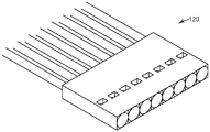
도 1c는 일부 실시예들에 따른 다중-도파관 광학 페룰의 사시도이다.
도 1d는 일부 실시예들에 따른, 도파관을 페룰에 고정하고 접근불가능 공간 내에 배치된 유연성 광학 접착제를 갖는 단일 도파관 광학 페룰의 단면도이다.
도 1e는 일부 실시예들에 따른, 도파관을 페룰에 고정하는 접착제 및 접근불가능 공간 내에 배치된 유연성 광학 재료를 갖는 단일 도파관 광학 페룰의 단면도이다.
도 1f 및 도 1g는 각각, 일부 실시예들에 따라 광학 페룰의 도파관 정지부와 연결된 도파관 특징부를 예시하는 광학 페룰의 단면도; 및
일부 실시예들에 따른 단일 도파관 광학 페룰의 단면도이다.
도 2a는 일부 실시예들에 따른 광학 페룰의 사시도이다.
도 2b는 도 2a의 광학 페룰의 평면도이다.
도 2c는 도 2a의 광학 페룰의 다른 사시도이다.
도 3a는 일부 실시예들에 따른 광학 페룰의 사시도이다.
도 3b는 도 3a의 광학 페룰의 평면도이다.
도 3c는 도 3a의 광학 페룰의 다른 사시도이다.
도 4는 다양한 실시예들에 따른, 센터링 배열을 갖는 복합 홈을 포함하는 광학 페룰의 일부분을 예시한다.
도 5는 광 도파관을 수용하도록 구성된 도 4에 도시된 복합 홈의 다양한 세부 사항들을 예시한다.
도 6은 도 4에 도시된 홈의 종방향 전이 섹션을 예시한다.
도 7은 다양한 실시예들에 따른, 전방 접착제 공동을 포함하는 광학 페룰 부착 영역의 평면도이다.
도 8은 도 7에 도시된 광학 페룰 부착 영역의 측면도이다.
도 9는 다양한 실시예들에 따른, 측방향 접착제 공동들을 포함하는 광학 페룰 부착 영역의 평면도이다.
도 10은 도 9에 도시된 광학 페룰 부착 영역의 측면도이다.
도 11은 다양한 실시예들에 따른, 공유된 전방 접착제 저장소를 포함하는 광학 페룰 부착 영역의 평면도이다.
도 12 내지 도 18은 다양한 실시예들에 따른, 광학 페룰 부착 영역의 복합 홈 내에 도파관을 설치하는 프로세스를 예시한다.
도 19는 복합 홈 내에 도파관을 설치하는 경우에 발생할 수 있는 정렬 오차를 예시한다.
도 20은 다양한 실시예들에 따른, 도 19에 예시된 정렬 오차의 감소를 용이하게 하는 리세스된 하부 표면 및 포치(porch) 구역을 갖는 홈을 도시한다.
도 21 내지 도 23은 다양한 실시예들에 따른, 센터링 표면들을 포함하는 각도 정렬 섹션 및 종방향 전이 섹션을 포함하는 두 개의 별개의 섹션들을 갖는 홈을 도시한다.
도 24는 다양한 실시예들에 따른 위치결정(positioning) 배열을 갖는 복합 홈을 포함하는 광학 페룰을 예시한다.
도면은 반드시 일정한 축척으로 작성된 것은 아니다. 도면에 사용되는 동일한 도면 부호는 동일한 컴포넌트를 지시한다. 그러나, 주어진 도면에서 소정 구성요소를 지시하기 위한 도면 부호의 사용은 동일한 도면 부호로 표지된 다른 도면의 그 구성요소를 제한하도록 의도되지 않음이 이해될 것이다.Figure 1a is a cross-sectional view of a single fiber optical ferrule according to some embodiments.
1B is a perspective view of the optical ferrule of FIG. 1A.
1C is a perspective view of a multi-waveguide optical ferrule according to some embodiments.
1D is a cross-sectional view of a single waveguide optical ferrule with a flexible optical adhesive disposed within the inaccessible space, securing the waveguide to the ferrule, in accordance with some embodiments.
FIG. IE is a cross-sectional view of a single waveguide optical ferrule with a flexible optical material disposed in an inaccessible space and an adhesive to secure the waveguide to the ferrule, in accordance with some embodiments.
1F and 1G are cross-sectional views of an optical ferrule, respectively, illustrating a waveguide feature connected with a waveguide stop of an optical ferrule, in accordance with some embodiments; And
Sectional view of a single waveguide optical ferrule according to some embodiments.
2A is a perspective view of an optical ferrule according to some embodiments.
Figure 2b is a top view of the optical ferrule of Figure 2a.
Figure 2c is another perspective view of the optical ferrule of Figure 2a.
3A is a perspective view of an optical ferrule according to some embodiments.
Figure 3b is a top view of the optical ferrule of Figure 3a.
Figure 3c is another perspective view of the optical ferrule of Figure 3a.
Figure 4 illustrates a portion of an optical ferrule including a composite groove with a centering arrangement, according to various embodiments.
Figure 5 illustrates various details of the composite groove shown in Figure 4 configured to accommodate the light pipe.
Figure 6 illustrates a longitudinal transition section of the groove shown in Figure 4;
7 is a plan view of an optical ferrule attachment region comprising a front adhesive cavity, in accordance with various embodiments.
8 is a side view of the optical ferrule attachment region shown in Fig.
9 is a top view of an optical ferrule attachment region comprising lateral adhesive cavities, in accordance with various embodiments.
10 is a side view of the optical ferrule attachment region shown in Fig.
11 is a top view of an optical ferrule attachment region comprising a shared front adhesive reservoir, in accordance with various embodiments.
Figures 12-18 illustrate a process for installing a waveguide in a composite groove in an optical ferrule attachment region, in accordance with various embodiments.
19 illustrates alignment errors that can occur when a wave guide is installed in a composite groove.
Figure 20 shows a groove with a recessed bottom surface and porch zone to facilitate reduction of the alignment error illustrated in Figure 19, in accordance with various embodiments.
Figures 21-23 illustrate grooves having two distinct sections, including an angular alignment section including centering surfaces and a longitudinal transition section, in accordance with various embodiments.
24 illustrates an optical ferrule including a composite groove having a positioning arrangement according to various embodiments.
The drawings are not necessarily drawn to scale. The same reference numerals used in the drawings indicate the same components. It is to be understood, however, that the use of reference numerals to designate certain elements in a given drawing is not intended to limit those elements of other drawings labeled with the same reference numerals.
유리 광섬유들이 인덱스-매칭된 접착제를 사용하여 중합체 광학 페룰들과 같은 광학 페룰들에 부착되는 경우에, 섬유의 팁으로부터 및/또는 페룰의 광 영향 요소의 광학 입력 표면으로부터 접착제의 탈층(delamination)의 문제들이 일어날 수 있다. 전형적으로 이들 시스템에서, 섬유는 광학 입력 표면과 접촉하도록 밀리고, 섬유 팁과 광 영향 요소의 광학 입력 표면 사이에 매우 얇은 층의 접착제를 남기게 된다. 상이한 열팽창, 접착제 수축, 및/또는 기계적 힘은 이러한 계면 상에 스트레스를 가하여 접착 실패를 야기할 수 있다.In the case where glass optical fibers are attached to optical ferrules such as polymeric optical ferrules using index-matched adhesives, the delamination of the adhesive from the tip of the fiber and / or from the optical input surface of the optical influencing element of the ferrule Problems can arise. Typically in these systems, the fibers are pushed into contact with the optical input surface, leaving a very thin layer of adhesive between the fiber tip and the optical input surface of the light influencing element. Different thermal expansions, adhesive shrinkage, and / or mechanical forces can stress this interface and cause adhesion failure.
본 명세서에 개시된 실시예들은 도파관의 단부와 광학 입력 표면 사이의 도파관 접근불가능 공간(waveguide inaccessible space)을 갖는 광학 페룰들(또한 광 결합 유닛들 또는 LCU들로도 지칭됨)에 관한 것이다. 개시된 접근법들은 도파관의 팁과 광학 입력 표면 사이의 도파관 접근불가능 공간에 비교적 유연성인 재료의 저장소를 제공함으로써 탈층의 문제를 완화한다. 일부 실시예들에서, 본 명세서에 개시된 접근법들은 y-홈 또는 종래의 v-홈, u-홈, 또는 원통형-구멍의 섬유 위치결정 시스템들과 함께 사용될 수 있다. 일부 실시예들에서, 본 명세서에 개시된 접근법들은 홈들 내의 도파관 위치를 제어하기 위해 센터링 측벽들을 갖는 홈들과 함께 사용될 수 있다.The embodiments disclosed herein relate to optical ferrules (also referred to as optical coupling units or LCUs) having a waveguide inaccessible space between the end of the waveguide and the optical input surface. The disclosed approaches mitigate the problem of delamination by providing a relatively flexible reservoir of material in the waveguide inaccessible space between the tip of the waveguide and the optical input surface. In some embodiments, the approaches disclosed herein may be used with fiber positioning systems of y-grooves or conventional v-grooves, u-grooves, or cylindrical-holes. In some embodiments, the approaches disclosed herein may be used with grooves having centering sidewalls to control waveguide locations within the grooves.
본 명세서에서 용어 "도파관" 또는 "광 도파관"은 신호 광을 전파하는 광학 요소를 지칭하는데 사용된다. 광 도파관은 클래딩을 갖는 적어도 하나의 코어를 포함하며, 코어 및 클래딩은 예컨대, 내부 전반사에 의해 코어 내에서 광을 전파하도록 구성된다. 광 도파관은 예를 들어 단일 또는 다중 모드 도파관, 단일 코어 섬유, 다중 코어 광섬유 또는 중합체 도파관일 수 있다. 도파관은 임의의 적절한 단면 형상, 예컨대, 원형, 정사각형, 직사각형 등을 가질 수 있다.The term "waveguide" or "optical waveguide" is used herein to refer to an optical element that propagates signal light. The optical waveguide comprises at least one core with cladding, the core and the cladding being configured to propagate light in the core, e.g., by total internal reflection. The light waveguide can be, for example, a single or multimode waveguide, a single core fiber, a multicore fiber or a polymeric waveguide. The waveguide may have any suitable cross-sectional shape, e.g., a circle, a square, a rectangle, and the like.
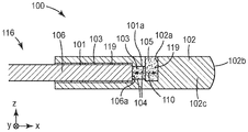
도 1a 및 도 1b는 일부 실시예들에 따른 광학 페룰(100)의 단면도와 사시도이다. 광학 페룰(100)은 광 도파관(106)을 수용하고 고정하도록 구성된 적어도 하나의 수용 요소(101)를 포함한다. 예를 들어, 도 1a에 도시된 바와 같이, 수용 요소(101)는 구멍, 예컨대, 도파관(106)의 직경보다 큰 직경을 갖는 실질적으로 원통형 구멍을 포함할 수 있다. 광학 페룰(100)은 적어도 하나의 광 영향 요소(102)를 포함한다. 도 1a 및 도 1b에 도시된 바와 같이, 광 영향 요소(102)는 입력 표면(102a), 렌즈(102b), 및 입력 표면(102a)과 렌즈(102b) 사이의 중간 섹션(102c)을 포함할 수 있다. 광 영향 요소(102)는 도파관(106)으로부터 광학 페룰(100) 내에 전파되는 광의 하나 이상의 특성들에 영향을 미친다. 예를 들어, 광 영향 요소에 의해 영향을 받는 광의 하나 이상의 특성들은 도파관(106)으로부터의 광의 방향 및/또는 발산을 포함할 수 있다.1A and 1B are a cross-sectional view and a perspective view of an
광섬유(116)는 코어, 예컨대, 유리 코어, 및 유리 클래딩을 갖는 도파관(106)을 포함하며, 코어 및 클래딩은 내부 전반사에 의해 코어 내에 광을 전파하도록 구성된다. 버퍼 코팅(도시되지 않음)은 광섬유(116)의 도파관(106)의 일부분들을 둘러쌀 수 있다. 일부 실시예들에서, 광섬유는 또한 재킷을 포함한다. 도 1a 내지 도 1c에 도시된 바와 같이, 광섬유(116)의 도파관(106) 만이 수용 요소(101) 내로 삽입되도록 버퍼 코팅 및 광섬유(116)의 재킷이 박리될 수 있다.The
도파관(106)이 수용 요소 내에 설치되는 경우에, 도파관의 출력 표면(106a)(또한, 본 명세서에서 "도파관의 말단 단부"로도 지칭됨)은 광 영향 요소(102)의 입력 표면(102a)에 광학적으로 결합된다. 도파관(106)은 도파관(106)의 출력 표면(106a)과 광 영향 요소(102)의 입력 표면(102a) 사이의 공간(103)에 접근불가능하다.The
도파관 정지부(104)는 수용 요소(101)와 광 영향 요소(102) 사이에 배치될 수 있다. 도파관 정지부(104)는 x축을 따른 광 영향 요소를 향한 도파관(106)의 이동을 제한한다. 도 1a에 도시된 바와 같이, 도파관 정지부(104)는, 구멍의 직경이 도파관(106)의 직경보다 작은, 구멍(101)을 따른 위치를 포함할 수 있다. 도파관 정지부(104)는 도파관(106)의 출력 표면(106a)의 x축을 따른 광 영향 요소(102)의 입력 표면(102a)을 향한 추가 이동을 제한한다. 도파관 정지부(104)는 도파관(106) 및/또는 페룰(100)에 대한 손상 없이 도파관(106)이 구멍(101) 내에서 더 밀릴 수 없도록 x축을 따른 도파관(106)의 추가 이동을 제한한다.The
일부 실시예들은 유연성 재료가 수용 요소(101) 내에 배치될 수 있도록 구성된 액세스 포트(105)를 포함한다.Some embodiments include an
일부 실시예들에서, 도파관 정지부(104)는 도파관(106)의 출력 표면(106a)과 광 영향 요소(102)의 입력 표면(102a) 사이의 x축을 따른 거리(110)가 약 10 μm 초과, 약 40 μm 초과, 약 80 μm 초과, 심지어 약 160 μm 초과가 되게 도파관(106)의 추가 이동을 정지시키도록 구성된다. 일부 실시예들에서, 도파관 정지부(104)와 광 영향 요소(102)의 입력 표면(102a) 사이의 거리는 약 10 μm 초과, 약 40 μm 초과, 약 80 μm 초과, 심지어 약 160 μm 초과이다.In some embodiments, the
일부 실시예들에서, 도파관 접근불가능 공간(103)의 적어도 일부분은 하나 이상의 유연성 재료들을 포함하는 저장소를 형성한다. 예를 들어, 저장소(103)는 광학 접착제, 광학 젤, 또는 광학 오일과 같은 유연성 광학 재료로 채워질 수 있다. 유연성 광학 재료는 도파관(106)으로부터의 광이 도파관(106)의 출력 표면(106a)과 광 영향 요소(102)의 입력 표면(102a) 사이의 접근불가능 공간(103)을 통해 전파되게 한다.In some embodiments, at least a portion of the waveguide
일부 실시예들에서, 유연성 광학 접착제(119)는 도파관(106)을 페룰(100)에 고정하는 데 사용될 수 있고, 유연성 광학 접착제(119)는 또한 도 1d에 예시된 바와 같이, 접근불가능 공간(103) 내에 배치될 수 있다. 일부 구현예들에서, 도 1e에 예시된 바와 같이, 광학 재료(118), 예컨대, 인덱스 오일 또는 젤과 같은 유연성 광학 재료는 접근불가능 공간(103) 내에 배치될 수 있으며, 광학 재료(118)는 도파관(106)을 페룰(100)에 본딩시키는 데 사용되는 접착제(117)와 상이하다. 도파관이 접근불가능 공간(103)을 채우는데 본딩 접착제(117)가 사용되지 않는 경우에, 본딩 접착제(117)는 광학 접착제일 수도 있지만, 반드시 광학 접착제일 필요는 없으며, 즉, 본딩 접착제(117)는 광 도파관(106)으로부터의 광에 대해 투명할 필요가 없다.In some embodiments, a flexible optical adhesive 119 may be used to secure the
도 1a 및 도 1b에 도시된 광학 페룰(100)은 단일 광섬유 페룰로서 예시되었지만, 도 1a 및 도 1b에 도시된 것과 유사한 구조가 도 1c에 도시된 바와 같은 다중-섬유 광학 페룰(120)을 형성하기 위해 복제될 수 있다.Although the
위의 도 1a에 예시된 바와 같이, 도파관 정지부는, 구멍의 직경이 도파관의 말단(출력) 단부의 직경보다 작은, 구멍을 따른 위치를 포함할 수 있다. 이 시나리오에서, 도파관 정지부의 위치는 도파관의 말단 단부의 위치와 같거나 실질적으로 같을 수 있다. 일부 실시예들에서, 도파관(또는 도파관 어레이)은 도파관의 말단 단부가 아닌 특징부를 포함할 수 있으며, 예컨대, 도파관 말단 단부로부터 이격되고, 도파관의 광 영향 요소의 입력 표면을 향한 추가 이동을 제한하기 위해 광학 페룰의 도파관 정지부와 연결된 돌출부를 포함할 수 있다. 예를 들어, 일부 실시예들에서, 도파관들은 광 영향 요소의 입력 표면을 향한 도파관의 출력 표면의 추가 이동을 제한하기 위해 광학 페룰 상의 도파관 정지 특징부들과 정합되는 도파관 어레이 상의 디봇(divot), 돌출부, 관통-구멍, 포스트, 또는 콜릿(collet)과 같은 특징부들을 포함하는 평면 도파관 어레이를 포함할 수 있다.As illustrated in FIG. 1A above, the waveguide stop may include a position along the hole where the diameter of the hole is smaller than the diameter of the end (output) end of the waveguide. In this scenario, the position of the waveguide stop may be the same as or substantially the same as the position of the distal end of the waveguide. In some embodiments, the waveguide (or waveguide array) may include features that are not the distal ends of the waveguide, and may, for example, be spaced from the waveguide distal end and may be configured to limit further movement of the optical effect elements of the waveguide toward the input surface And a protrusion connected to the waveguide stop of the weir optical ferrule. For example, in some embodiments, the waveguides include a divot on a waveguide array that is matched with waveguide stop features on the optical ferrule to limit further movement of the output surface of the waveguide toward the input surface of the light influencing element, , A through-hole, a post, or a collet.
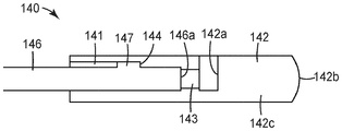
도 1f 및 도 1g는 일부 실시예들에 따른 광학 페룰들(130, 140)의 단면도들이다. 광학 페룰(130, 140)은 광 도파관(136, 146)을 수용하고 고정하도록 구성된 적어도 하나의 수용 요소, 예컨대, 구멍(131, 141)을 포함한다. 광학 페룰(130, 140)은 적어도 하나의 광 영향 요소(132, 132)를 포함한다. 광 영향 요소(132, 132)는 입력 표면(132a, 142a), 렌즈(132b, 142b), 및 입력 표면(132a, 142a)과 렌즈(132b, 142b) 사이의 중간 섹션(132c, 142c)을 포함할 수 있다. 광 영향 요소(132, 142)는 도파관(136, 146)으로부터 광학 페룰(130, 140) 내로 전파되는 광의 하나 이상의 특성들에 영향을 미친다.1F and 1G are cross-sectional views of
도파관(136, 146)이 수용 요소(131, 141) 내에 설치되는 경우에, 도파관의 출력 표면(136a, 146a)은 광 영향 요소(132, 142)의 입력 표면(132a, 142a)에 광학적으로 결합된다. 도파관(136, 146)은 도파관(136, 146)의 출력 표면(136a, 136a)과 광 영향 요소(132, 142)의 입력 표면(132a, 142a) 사이의 공간(133, 143)에 접근불가능하다.The
도파관 정지부(134, 144)는 수용 요소(131, 141)와 광 영향 요소(132, 142) 사이에 배치될 수 있다. 도파관 정지부(134, 144)는 x축을 따른 광 영향 요소(132, 142)를 향한 도파관(136, 146)의 이동을 제한한다. 도 1f 및 도 1g에 도시된 바와 같이, 도파관 정지부(134, 144)는, 구멍의 측면들이 도파관(136, 146)의 돌출 특징부(137, 147)에 연결되는, 구멍(131, 141)을 따른 위치를 포함할 수 있다. 도파관 정지부(134, 144)와의 돌출 특징부(137, 147)들의 연결은 도파관(136, 146)의 출력 표면(136a, 146a)의 x축을 따른 광 영향 요소(132, 142)의 입력 표면(132a, 142a)을 향한 추가 이동을 제한한다. 돌출 특징부(137)는 도 1f에 도시된 바와 같이, 광섬유의 대칭적 에치(etch)일 수 있다. 대안적으로, 돌출 특징부(147)는 도 1g에 도시된 바와 같이, 단일면일 수 있는데, 예컨대, 돌출 특징부는 평면 도파관의 단일면 에치에 의해 형성될 수 있다.The waveguide stops 134 and 144 may be disposed between the receiving
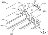
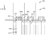
도 2a, 도 2b, 및 도 2c는 일부 실시예들에 따른 광학 페룰(200)의 사시도, 평면도 및 다른 사시도이다. 광학 페룰(200)은 광 도파관(206)을 수용하고 고정하도록 구성된 적어도 하나의 수용 요소(201)를 포함한다. 도 2a 내지 도 2c에서, 광학 페룰(200)의 수용 요소(201)는 V자형 홈으로 도시된다. 대안적으로, 홈은 U자형, Y자형 또는 임의의 다른 적합한 형상을 가질 수 있다.2A, 2B and 2C are a perspective view, a plan view and another perspective view of an
광학 페룰(200)은 적어도 하나의 광 영향 요소(202)를 포함한다. 도 2a 내지 도 2c에 도시된 바와 같이, 광 영향 요소(202)는 입력 표면(202a), 광 방향전환(redirecting) 요소(202b), 및 입력 표면(202a)과 광 방향전환 요소(202b) 사이의 중간 섹션(202c)을 포함할 수 있다. 광 도파관(206)이 수용 요소(201) 내에 설치되는 경우에, 광 도파관의 출력 표면(206a)은 광 영향 요소(202)의 입력 표면(202a)에 광학적으로 결합된다. 광 영향 요소(202)는 도파관(206)으로부터 광학 페룰(200) 내에 전파되는 광의 하나 이상의 특성들에 영향을 미친다.The
광섬유(216)는 코어, 예컨대, 유리 코어, 및 유리 클래딩을 갖는 도파관(206)을 포함하며, 코어 및 클래딩은 내부 전반사에 의해 코어 내에 광을 전파하도록 구성된다. 버퍼 코팅(206b)은 광섬유(216)의 도파관(206)을 둘러싼다. 일부 실시예들에서, 광섬유는 또한 재킷(206c)을 포함한다. 도 2a 내지 도 2c에 도시된 바와 같이, 광섬유(216)의 도파관(206) 만이 수용 요소(201) 내로 삽입되도록 버퍼 코팅(206b) 및 광섬유(216)의 재킷(206c)이 박리될 수 있다. 광섬유(216)의 도파관(206)은 공간(203)에 접근불가능하다.The
일부 실시예들에서, 페룰(200)은 도파관(206) 및/또는 페룰(200)에 대한 손상 없이 도파관(206)이 홈(201)을 따라 더 밀릴 수 없도록 x축을 따른 도파관(206)의 추가 이동을 제한하는 도파관 정지부(204)를 포함한다. 도 2a 내지 도 2c에 도시된 바와 같이, 도파관 정지부(204)는 접착제 또는 다른 유연성 재료를 위한 개구부(205)를 갖는 벽을 포함할 수 있다. 도파관(206)은 도파관(206)의 출력 표면(206a)과 광 영향 요소(202)의 입력 표면(202a) 사이의 공간(203)에 접근불가능하다. 일부 실시예들에서, 도파관 정지부(204)는 도파관(206)의 출력 표면(206a)과 광 영향 요소(202)의 입력 표면(202a) 사이의 x축을 따른 거리(210)가 약 10 μm 초과, 약 40 μm 초과, 약 80 μm 초과, 심지어 약 160 μm 초과가 되게 도파관(206)의 추가 이동을 정지시키도록 구성된다. 접근불가능 공간(203)은 광학 접착제, 광학 젤, 또는 광학 오일과 같은 유연성 광학 재료로 채워질 수 있다. 예를 들어, 광학 접착제가 사용되어 도파관(206)을 페룰(200)에 고정할 수 있다. 예를 들어, 유연성 재료는 도파관(206)으로부터의 광이 도파관(206)의 출력 표면(206a)과 광 영향 요소(202)의 입력 표면(202a) 사이의 접근불가능 공간(203)을 통해 실질적으로 방해 없이 전파되도록 선택될 수 있다.In some embodiments, the
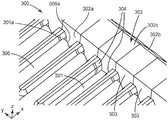
도 3a, 도 3b, 및 도 3c는 일부 실시예들에 따른 광학 페룰(300)의 사시도, 평면도 및 다른 사시도이다. 광학 페룰(300)은 광 도파관(306)을 수용하고 고정하도록 구성된 적어도 하나의 수용 요소(301)를 포함한다. 도 3a 내지 도 3c에서, 광학 페룰(300)의 수용 요소(301)는 센터링 측벽들(301a)을 갖는 Y자형 홈으로 도시된다. 센터링 측벽들(301)은 도파관(306)을 광 영향 요소(302)의 입력 표면(302a)에 대해 y축을 따라 중심설정하도록 각도를 갖는다.3A, 3B, and 3C are a perspective view, a top view, and another perspective view of an
광학 페룰(300)은 적어도 하나의 광 영향 요소(302)를 포함한다. 도 3a 내지 도 3c에 도시된 바와 같이, 광 영향 요소(302)는 입력 표면(302a), 광 방향전환 요소(302b), 및 입력 표면(302a)과 광 방향전환 요소(302b) 사이의 중간 섹션(302c)을 포함할 수 있다. 광 영향 요소(302)는 도파관(306)으로부터 광학 페룰(300) 내에 전파되는 광의 하나 이상의 특성들에 영향을 미친다.The
페룰(300)은 도파관(306)의 x축을 따른 광 영향 요소의 입력 측면(302a)을 향한 추가 이동을 방지하도록 구성되는 도파관 정지부(304)를 포함한다. 도파관 정지부(304)는 도파관(306)이 도파관(306) 및/또는 페룰(300)에 대한 손상 없이 홈(301) 내에서 광 영향 요소(302)의 입력 측면(302a)을 향해 추가로 밀리지 않게 방지한다. 도 3a 내지 도 3c에 도시된 바와 같이, 도파관 정지부(304)는, 도파관 정지부(304)에서의 홈(301)의 측벽들 사이의 거리가 도파관(306)의 직경보다 작아지는, 센터링 특징부들(301a)을 따른 위치를 포함할 수 있다. 도파관(306)은 도파관(306)의 출력 표면(306a)과 광 영향 요소(302)의 입력 표면(302a) 사이의 공간(303)(도 3b에 도시됨)에 접근불가능하다. 일부 실시예들에서, 도파관 정지부(304)는 도파관(306)의 출력 표면(306a)과 광 영향 요소(302)의 입력 표면(302a) 사이의 x축을 따른 거리(310)가 약 10 μm 초과, 약 40 μm 초과, 약 80 μm 초과, 심지어 약 160 μm 초과가 되게 도파관(306)의 추가 이동을 정지시키도록 구성된다.The
접근불가능 공간(303)(도 3b 참조)은 광학 접착제, 광학 젤, 또는 광학 오일과 같은 유연성 광학 재료로 채워질 수 있다. 예를 들어, 광학 접착제가 사용되어 도파관(306)을 페룰(300)에 고정할 수 있다. 유연성 광학 재료는 도파관(306)으로부터의 광이 도파관(306)의 출력 표면(306a)과 광 영향 요소(302)의 입력 표면(302a) 사이의 접근불가능 공간(303)(도 3b 참조)을 통해 실질적으로 방해 없이 전파되게 한다.The inaccessible space 303 (see FIG. 3B) may be filled with a flexible optical material, such as an optical adhesive, an optical gel, or an optical oil. For example, an optical adhesive may be used to secure the
광 도파관들 또는 섬유들을 광학 또는 광전자 디바이스들에 부착하는 것은 종종 V자형 홈들(예컨대, V-홈들)을 사용하여 수행된다. 도파관들은 클램핑 메커니즘을 사용하여 홈의 바닥(전형적으로 90° 각도 V-홈) 내로 억지로 끼워 맞춰진다. 전형적으로, V-홈 내에 도파관들을 영구적으로 유지하기 위해 인덱스 매칭 접착제가 이어서 도포된다. 이 스킴은 몇 가지 문제점들을 갖는다. 클램핑 메커니즘은 도파관들을 굴곡시켜 이들을 홈들에 안착시키고 따라서 이들을 홈들과 정렬시키기에 충분한 힘을 제공하는 반면, 도파관들의 리본의 각각의 도파관에 접촉하기에 충분한 유연성을 가지고 있어야 한다. 이는 또한 접착제 자체가 도파관들에 본딩되지 않고 도포되기 위한 접근을 허용해야 한다. V-홈들 위의 클램핑 메커니즘의 위치는 도파관들의 위치들을 관찰하거나 광 경화 접착제를 사용하는 것을 어렵게 만든다. 평평한 저부들 및 수직 측벽들을 갖는 U자형 홈들(즉, U-홈들)의 사용에는 몇 가지 문제점들이 있다. 도파관들의 용이한 포획 및 홈 폭에 요구되는 클리어런스와 연관된 위치 오차에 대한 문제점들은 이전에 언급되지 않았다.Attaching light waveguides or fibers to optical or optoelectronic devices is often accomplished using V-shaped grooves (e.g., V-grooves). The waveguides are forced into the bottom of the groove (typically 90 ° angle V-groove) using a clamping mechanism. Typically, an index matching adhesive is subsequently applied to permanently retain the waveguides in the V-groove. This scheme has several problems. The clamping mechanism must have sufficient flexibility to contact waveguides of each of the ribbons of the waveguides, while providing sufficient force to bend the waveguides and seat them in the grooves and thus align them with the grooves. It should also allow access for the adhesive itself to be applied without being bonded to the waveguides. The position of the clamping mechanism on the V-grooves makes it difficult to observe the positions of the waveguides or to use a light curing adhesive. There are several problems with the use of U-shaped grooves (i.e., U-grooves) with flat bottoms and vertical sidewalls. Problems with positional errors associated with clearance required for easy trapping and groove widths of waveguides have not been previously discussed.
실시예들은 하나 또는 다수의 광 도파관들을 수용하고 영구적으로 부착되도록 구성된 하나 또는 다수의 홈들을 갖는 광 결합 유닛에 관한 것이다. 일 실시예에서, 홈의 일부분은 광 도파관이 측방향으로 굴곡되어 올바른 위치 내로 들어가도록 허용하는 거의 수직인 측벽들을 제공한다. 홈은 상부에서 더 넓게 형성되어, 광 도파관을 홈 내로 포획하는 것을 용이하게 하는 실질적으로 Y자형 단면(즉, Y-홈)을 제공할 수 있다. 전술한 바와 같이, 광 도파관들은 단일 모드 광 도파관들, 다중 모드 광 도파관들 또는 단일 모드 또는 다중 모드 광 도파관들의 어레이일 수 있다. 일부 실시예들에서, 도파관들은 단일 모드 또는 다중 모드 중합체 광 도파관이다.Embodiments relate to an optical coupling unit having one or more grooves configured to receive and permanently attach one or more optical waveguides. In one embodiment, a portion of the groove provides substantially vertical sidewalls that allow the light waveguide to flex laterally into the correct position. The grooves may be formed wider at the top to provide a substantially Y-shaped cross-section (i.e., Y-groove) that facilitates capturing the optical waveguide into the grooves. As discussed above, optical waveguides may be single mode optical waveguides, multimode optical waveguides, or an array of single mode or multimode optical waveguides. In some embodiments, the waveguides are single mode or multimode polymer optical waveguides.
다른 실시예에서, 홈의 일부분은 광 도파관이 측방향으로 굴곡되어 올바른 위치 내로 들어가도록 허용하는 거의 수직인 측벽들을 제공한다. 홈의 이 부분은 광 도파관의 초기 포획을 위한 클리어런스를 제공하기 위해 광 도파관의 직경보다 약간 넓게 만들어질 수 있다. 일단 홈의 저부와 접촉하고 그와 대략 평행하게 되면, 광 도파관의 단부는 홈의 폭이 광 도파관의 직경 미만으로 점차 좁아지는 위치로 축방향으로 슬라이딩된다. 여기에서 광 도파관의 팁이 정지하고 올바르게 위치된다. 일부 실시예들에 따르면, 홈은 상부에서 더 넓게 형성되어, 광 도파관을 홈 내로 포획하는 것을 용이하게 하는 실질적으로 Y자형 단면을 제공할 수 있다.In another embodiment, a portion of the groove provides substantially vertical sidewalls that allow the light waveguide to flex laterally into the correct position. This portion of the groove can be made slightly wider than the diameter of the light pipe to provide a clearance for the initial capture of the light pipe. Once in contact with and approximately parallel to the bottom of the groove, the end of the optical waveguide slides in the axial direction to a position where the width of the groove gradually narrows below the diameter of the optical waveguide. Here the tip of the light pipe stops and is correctly positioned. According to some embodiments, the grooves may be formed wider at the top to provide a substantially Y-shaped cross-section that facilitates capturing the optical waveguide into the grooves.
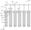
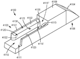
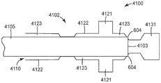
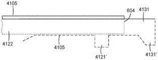
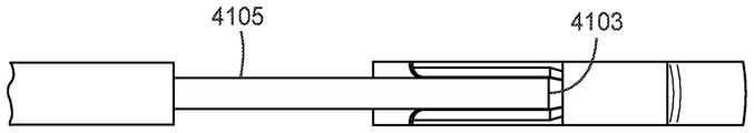
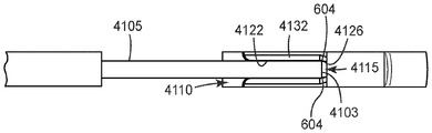
도 4는 다양한 실시예들에 따른 LCU(4100)의 일부분을 예시한다. 도 4에 도시된 LCU(4100)는 단일 LCU 부착 영역(4102)을 포함한다. 단일 LCU 부착 영역(4102)이 도 4에 도시되었지만, 다수의 광 도파관들을 수용하고 그에 영구적으로 부착되기 위해 다수의 부착 영역들(4102)이 LCU(4100) 상에 구비될 수 있음이 이해된다. LCU 부착 영역(4102)은 입구(4111), 말단 단부(4113) 및 입구(4111)와 말단 단부(4113) 사이에서 연장되는 중앙 평면(4112)(도 5 참조)을 갖는 Y-홈(4110)을 포함한다. 도 5에 도시된 바와 같이, 중앙 평면(4112)은 Y-홈(4110)의 하부 표면(4125)을 양분하고, 하부 표면(4125)으로부터 수직으로 연장된 평면이다. Y-홈(4110)은 도 5에 도시된 일반적으로 원통형인 도파관(4105)과 같은 광 도파관을 수용하도록 구성된다.4 illustrates a portion of an
LCU(4100)는 광 방향전환 부재(4104) 및 광 방향전환 부재(4104)와 말단 단부(4113) 사이의 중간 섹션(4108)을 포함한다. 일부 실시예들에서, 말단 단부(4113)는 렌즈와 같은 광학적으로 투명한(optically clear) 부재를 포함하거나 광학적으로 투명한(optically transparent) 재료로 형성된다. 중간 섹션(4108)은 광학적으로 투명한 재료로 형성된다. 광 방향전환 부재(4104)는 출력 측면(4106)을 포함하며, 이를 통해 광이 광 유도 부재(4104)로부터 방출(또는 그 내부로 진입)된다.The
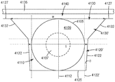
일부 실시예들에 따르면, 또한 도 4 및 도 5를 참조하면, Y-홈(4110)은 복합 홈으로서, 일반적으로 U자형 하부 부분(4120) 및 복합 홈을 일반적으로 Y자형으로 만드는 확장된 상부 부분에 의해 형성된다. 용어 "홈"을 수식하는 용어들 "U" 및 "Y"는 편리함을 목적으로 하여 이들 홈들의 대략적인 형상을 의미하는 기능을 하는 것이고 한정이 아님이 이해된다.4 and 5, the Y-
도 5에서 가장 잘 볼 수 있는 바와 같이, Y-홈(4110)은 제1 구역(4120'), 제2 구역(4130'), 개구부(4140) 및 하부 표면(4125)에 의해 정의된다. 제1 구역(4120')은 하부 표면(4125)과 제2 구역(4130') 사이에 정의된다. 제1 구역(4120')은 간격(S)만큼 분리된 실질적으로 평행한 측벽들(4122)을 포함한다. 측벽들(4122)은 수직 방향에서 1도 또는 몇 도(예컨대, < 약 10도)의 드래프트(draft)를 가질 수 있으며, 따라서 서로 실질적으로 평행한 것으로 간주될 수 있다. 예를 들어, 측벽들(4122)은 하부 표면(4125)에 대해 약 5도 이내로 수직일 수 있다. 측벽들(4122)은 제조 중에 측벽들(4122)의 이형을 용이하게 하기 위해 약간 외향인 경사 또는 드래프트를 가질 수 있다. 이 경우, 실질적으로 수직인 측벽들(4122)은 하부 표면(4125)으로부터 수직으로 연장되는 평면(4112)을 갖는 드래프트각(α)을 형성한다.As best seen in FIG. 5, the Y-
제2 구역(4130')은 제1 구역(4120')과 개구부(4140) 사이에 배치된다. 개구부(4140)는 Y-홈(4110)의 상부 표면들(4127) 사이에 정의된다. 개구부(4140)의 폭(W)은 측벽들(4122) 사이의 간격(S)보다 크다. 도 42에서 볼 수 있듯이, 제1 구역(4120')은 Y-홈(4110)의 U자형 하부 부분(4120)을 정의하고, 제2 구역(4130')은 확장된 상부 부분(4130)을 정의한다.The second zone 4130 'is disposed between the first zone 4120' and the
제2 구역(4130')은 Y-홈(4110)의 중앙 평면(4112)으로부터 외향으로 연장되는 측벽들(4132)을 포함한다. 도 42에서, 측벽들 (4132)은 선형 측벽들을 포함하고, 이들은 모따기된(chamfered) 측벽들로 간주될 수 있다. 다른 실시예들에서, 측벽들(4132)은 어느 정도의 곡률을 갖는 것과 같은 비선형일 수 있다. 측벽들(4132)은 제1 구역(4120')과 개구부(4140) 사이에서 연장되며, 측벽들(4132) 사이의 간격은 제1 구역(4120')으로부터 개구부(4140)로 점진적으로 증가한다.The second region 4130 'includes sidewalls 4132 that extend outwardly from the
일부 실시예들에 따르면, 개구부(4140)의 폭(W)은 제1 구역(4120')의 간격(S)보다 간격(S)의 약 절반과 동일한 거리만큼 더 크다. 다른 실시예들에서, 개구부(4140)의 폭(W)은 간격(S)보다 간격(S)의 절반보다 큰 거리만큼 크다. 제1 구역(4120')의 측벽들(4122)의 높이는 도파관(4105)의 높이의 약 50%보다 더 클 수 있다. 예를 들어, 제1 구역(4120')의 측벽들(4120)의 높이는 광 도파관(4105)의 높이의 약 50% 내지 75% 사이의 범위일 수 있다. 일부 실시예들에서, 제1 구역(4120')의 측벽들(4122)의 높이는 약 62.5 ㎛ 내지 65 ㎛ 초과이지만 광 도파관(4105)의 높이보다 낮을 수 있다. 다른 실시예들에서, 제1 구역(4120')의 측벽들(4122)의 높이는 약 75 ㎛ 초과이지만 광 도파관(4105)의 높이보다 낮을 수 있다. 도 5에 도시된 실시예에서, Y-홈(4110)의 전체 높이는 도파관(4105)의 높이(예컨대, 약 125 ㎛)와 대략 동일하다. 일부 실시예들에서, Y-홈(4110)의 전체 높이는 도파관(4105)의 높이보다 작거나 클 수 있다. 커버(4135)(옵션적임)는 LCU(4100)의 광 도파관들(4105) 및 홈들(4110)을 덮도록 구성될 수 있다.According to some embodiments, the width W of the
도 5에서 볼 수 있듯이, 광 도파관(4105)에 가장 근접하게 접근한 구역에서 제1 구역(4120')의 측벽들(4122) 사이의 간격은 도파관의 폭보다 미리 결정된 클리어런스만큼 크다. 일부 실시예들에서, 미리 결정된 클리어런스는 약 1 ㎛ 미만일 수 있다. 다른 실시예들에서, 미리 결정된 클리어런스는 약 1 ㎛ 내지 3 ㎛일 수 있다. 또 다른 실시예들에서, 미리 결정된 클리어런스는 약 1 ㎛ 내지 5 ㎛일 수 있다. 예를 들어, 광 도파관(4105)은 약 125 ㎛의 폭을 가질 수 있고, 제1 구역(4120')의 측벽들(4122)을 분리하는 간격은 약 1 ㎛ 내지 5 ㎛의 클리어런스를 포함할 수 있다.5, the spacing between the
다중 모드 섬유를 포함하는 도파관(4105)을 채용하는 실시예들에서, 미리 결정된 클리어런스는 약 1 ㎛ 내지 5 ㎛일 수 있다. 예를 들어, 미리 결정된 클리어런스는 다중 모드 섬유를 포함하는 광 도파관(4105)의 폭의 약 0.8% 내지 4%와 동일할 수 있다. 단일 모드 섬유를 포함하는 도파관(4105)을 채용하는 실시예들에서, 미리 결정된 클리어런스는 약 0 ㎛ 내지 2 ㎛일 수 있다. 예를 들어, 미리 결정된 클리어런스는 단일 모드 섬유를 포함하는 광 도파관(4105)의 폭의 약 0% 내지 1.6%와 동일할 수 있다. 일부 경우들에서, 클리어런스는 도파관(4105)이 Y-홈(4110) 내에 배치되는 경우에 Y-홈을 변형시키도록 0 미만일 수 있다.In
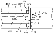
도 5 및 도 6에 도시된 도파관(4105)은 클래딩(4109)으로 둘러싸인 코어(4107)를 포함한다. 도파관(4105)이 광학적 (인덱스-매칭된) 본딩 재료를 사용하여 Y-홈(4110) 내의 제 위치에 영구적으로 본딩되는 경우에, 코어(4107)가 광 방향전환 부재(도 41의 4104 참조)와 광학적으로 정렬되는 것이 중요하다. 일부 실시예들에서, Y-홈(4110)은 센터링 배열을 포함하며, 이에 의해 도파관(4105)은 도파관(4105)이 Y-홈(4110) 내에 설치되는 경우에 Y-홈(4110)의 중심 평면(4112)을 향해 측방향으로 강제적으로 안내된다. Y-홈(4110)의 중심 평면(4112)을 따라 코어(4107)를 중심설정하는 것 이외에, 센터링 배열은 Y-홈(4110) 내에서 도파관(4105)의 축방향 변위를 제한하는 도파관 정지부를 제공한다. 따라서, 일부 실시예들에 따른 복합 Y-홈(4110)은 U-홈 단독 또는 Y-홈과 조합된 센터링 배열을 포함한다.The
도 4 및 도 6은 제1 단부(4115') 및 제2 단부(4115")를 포함하는 종방향 전이 섹션(4115)에 의해 정의된 센터링 배열을 포함하는 Y-홈(4110)을 도시한다. 제1 단부(4115')는 제1 구역(4120')의 측벽들(4122) 사이의 간격(S)과 동일한 폭을 갖는다. 제2 단부(4115")는 광 도파관(4105)의 폭보다 작은 폭을 갖는다. 측벽 간격은 예컨대 전이 섹션(4115) 내의 내향으로 각도를 갖는 측벽들에 의해 전이 섹션(4115) 내에서 점진적으로 감소한다. 전이 섹션(4115)은 측벽들(4122)의 말단 단부들로부터 시작하여 Y-홈(4110)의 중앙 평면을 향해 내향으로 돌출될 수 있는 센터링 측벽들(4126)을 포함한다. 센터링 측벽들(4126)은 Y-홈(4110)의 모따기된 측벽들로 간주될 수 있다. 전이 섹션(4115)의 측벽들(4122) 및 센터링 측벽들(4126)은 실질적으로 평면 측벽 표면들 또는 비-평면 측벽 표면들을 포함할 수 있다.Figures 4 and 6 illustrate a Y-
센터링 측벽들(4126)은 측벽들(4122)과 약 5도 내지 45도 범위일 수 있는 각도(β)를 형성한다. 종방향 전이 섹션(4115)은 Y-홈(4110)의 전체 길이에 비해 그다지 길 필요는 없다. 예를 들어, Y-홈(4110)의 길이는 200 ㎛ 내지 2000 ㎛일 수 있고, 센터링 측벽들(4126)은 측벽들(4122)로부터 약 2 ㎛ 내지 50 ㎛의 거리만큼 연장될 수 있다. 센터링 측벽들(4126)은 측벽들(4122)의 높이와 동일한 높이를 가질 수 있다.The centering sidewalls 4126 form an angle beta that may range from about 5 degrees to about 45 degrees with the
도파관(4105)이 Y-홈(4110) 내에서 광 방향전환 부재(4104)를 향해 축방향으로 변위됨에 따라, 도파관(4105)의 말단 단부(4103)는 센터링 측벽들(4126)과 접촉하고 Y-홈(4110)의 중심 평면을 향해 안내되어, 도파관(4105)의 중심 축이 Y-홈(4110) 내에서 중심설정된다. 갭(4129)은 센터링 측벽들(4126)의 말단 단부들 사이에 정의된다. 갭(4129)은 도파관(4105)의 코어(4107)로부터 나오는 광의 방해되지 않는 통로를 허용하기에 충분히 넓다. 센터링 측벽들(4126)의 길이 및 갭(4129)의 폭은 도파관(4105)의 코어 및 클래딩 치수들을 수용하는 크기로 하는 것이 바람직하다. 도파관(4105)의 말단 단부(4103)가 센터링 배열에 의해 Y-홈(4110) 내에서 적절히 중심설정되면, 클래딩(4109)은 도파관 정지부(604)의 위치에서 센터링 측벽들(4126)과 접촉되고, 코어(4107)는 갭(4129)의 중심과 정렬된다. 도 43에 도시된 센터링 배열은 U-홈 또는 Y-홈과 같은 복합 U-홈 내에 구현될 수 있음이 이해된다.As the
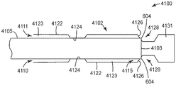
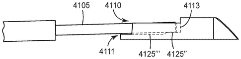
도 7은 다양한 실시예들에 따른 LCU(4100)의 LCU 부착 영역(4102)의 평면도를 도시한다. 도 7에 예시된 LCU 부착 영역(4102)은 Y-홈(4110) 내에 중심설정된 도파관(4105)의 말단 단부(4103)를 도시한다. 도 7에 예시된 Y-홈(4110)의 실시예는 Y-홈(4110)의 입구(4111)와 종방향 전이 섹션(4115) 사이의 정렬 특징부를 포함한다. 정렬 특징부는 홈 측벽들(4122)의 돌출 섹션(4124)을 포함한다. 대향하는 돌출 섹션들(4124) 사이의 공간은 도파관(4105)의 폭보다 약간 크고 대향 측벽들(4122) 사이의 간격보다 작다. 정렬 특징부의 돌출 섹션들(4124)은 도파관 단부(4103)가 Y-홈(4110)의 전이 섹션(4115) 내에 위치되는 경우에 Y-홈(4110)의 센트럴 평면에 대해 도파관(4105)의 각도 정렬을 제공하는 기능을 한다. 일부 실시예들에서, 돌출 섹션들(4124)에 의해 형성된 정렬 특징부는 홈 입구(4111)에, 또는 그 부근에 위치된다.Figure 7 shows a top view of an
도 7에 예시된 실시예에서, 도파관(4105)의 말단 단부(4103)의 에지들은 도파관 정지부(604)의 위치에서 전이 섹션(4115)의 센터링 벽들(4126)에 약간 매립된 것으로 도시되어 있다. 이 실시예에서, 도파관(4105)의 클래딩(4109)은 센터링 벽들(4126)을 형성하는데 사용되는 재료보다 경질인 재료(예컨대, 유리)로 형성된다. 도파관(4105)의 말단 단부(4103)가 그 중심 위치에서 센터링 벽들(4126)에 대향해 놓일 때 도파관(4105)에 축방향으로 지향된 힘을 가함으로써 센터링 벽들(4126)에 변형(4128)이 형성될 수 있다. 변형(4128)은 광학 본딩 재료가 도파관(4105)을 Y-홈(4110) 내에 영구적으로 본딩하도록 적용될 때 Y-홈(4110) 내에서 도파관(4105)이 적절한 중심설정된 위치결정을 유지하는 것을 돕는다.7, the edges of the
도 7에 도시된 Y-홈(4110)의 실시예는 Y-홈(4110)의 측벽들(4122)과 도파관(4105)의 외주 사이에 정의된 본딩 구역(4123)을 포함한다. 본딩 구역(4123)은, 경화되었을 때, Y-홈(4110) 내에 도파관(4105)을 영구적으로 본딩하는 본딩 재료(예컨대, 광학 본딩 재료)로 채워질 수 있다. 일부 실시예들에서, 본딩 구역(4123)은 도파관(4105), 평면 하부 표면(4125), 및 측벽들(4122) 사이의 체적으로 정의된다. 다른 실시예들에서, 하부 표면(4125)이 측벽들(4122)과 만나는 측벽들(4122)의 일부분을 따라 함몰부 또는 트러프(trough)가 형성되어 Y-홈(4110) 내에 포획된 본딩 재료의 체적을 증가시킬 수 있다.The embodiment of the Y-
도 7은 또한 광학 본딩 재료의 체적을 수용하도록 구성된 전방 접착제 공동(4131)을 도시하며, 광학 본딩 재료는 경화되었을 때, 도파관(4105)의 말단 단부(4103)와 LCU 부착 영역(4102) 사이의 본딩의 세기(예컨대, 완전성(integrity))를 증가시키는 기능을 한다. 일부 실시예들에서, 접착제 공동(4131)은 도파관(4105)의 단부로부터 광을 송신하도록 구성된다. 도 8에 도시된 바와 같이, 전방 접착제 공동(4131)은 LCU 부착 영역(4102)의 하부 표면(4125) 내로 형성된 함몰부(4131')를 포함할 수 있다. 함몰부(4131')는 광학 본딩 재료를 수용하기 위한 전방 접착제 공동(4131)의 총 체적을 증가시키는 기능을 하여 도파관(4105)의 말단 단부(4103)와 LCU 부착 영역(4102) 사이의 본딩의 세기/완전성을 향상시킨다. 도 9는 또한 홈(110)의 하부 표면(4125)이 경사에서 평탄역(plateau)으로 전이하는 위치(4133)에서의 Y-홈(4110)의 입구(4111)를 도시한다.Figure 7 also shows a front
도 9는 도 7에 예시된 본딩 구역들(4123) 및 전방 접착제 공동(4131)을 도시하고, 부가적으로, Y-홈(4110)의 각각의 측벽(4122)으로부터 측방향으로 연장되는 측방향 접착제 공동(4121)을 도시한다. 측방향 접착제 공동들(4121)은 본딩 구역들(4123)의 연장된 부분들일 수 있다. 측방향 접착제 공동들(4121)은 도파관(4105)의 말단 단부(103)의 측면들 근처에 부가적인 본딩 재료를 수용하기 위한 체적을 제공하며, 이는 Y-홈(4110)과 도파관(4105) 사이의 본딩의 세기/완전성을 증가시킨다. 도 10에 도시된 바와 같이, 측방향 접착제 공동(4121)은 LCU 부착 영역(4102)의 하부 표면(4125) 내로 형성된 함몰부(4121')를 포함할 수 있다. 함몰부(4121')는 광학 본딩 재료를 수용하기 위한 측방향 접착제 공동(4121)의 총 체적을 증가시킴으로써 도파관(4105)과 Y-홈(4110) 사이의 본딩의 세기/완전성을 향상시키는 기능을 한다.9 illustrates the
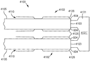
도 11은 각각 그 내부에 도파관(4105)이 배치된 다수의 홈들(4110)을 포함하는 LCU 부착 영역(4102)을 예시한다. 도 11에서, 두 개의 홈들(4110)이 예시되어 있으며, 각자의 도파관들(4105)은 도파관 정지부(604)의 위치에서 홈들(4110) 내의 중심설정된 위치에서 센터링 표면들(4126)과 접촉되어 있다. 도 11은 전방 접착제 공동들(4131)에 인접하여 위치된 접착제 저장소(4131")를 도시한다. 접착제 저장소(4131")는 전방 접착제 공동들(4131) 중 두 개 이상 사이에서 공유되는 LCU 부착 영역(4102)의 체적이다. 이와 관련하여, 접착제 저장소(4131")는 두 개 이상의 전방 접착제 공동들(4131)에 유체적으로 결합된다(fluidically coupled). 접착제 저장소(4131")는 도파관들(4105)의 말단 단부들(4103) 근처에 부가적인 본딩 재료를 수용하기 위한 체적을 제공하며, 이는 도파관(4105)과 LCU 부착 영역(4102) 사이의 본딩의 세기/완전성을 증가시킨다.Figure 11 illustrates an
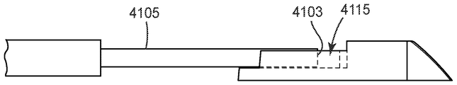
도 12 내지 도 17은 다양한 실시예들에 따른, LCU 부착 영역(4102)의 Y-홈(4110)에 도파관(4105)을 설치하기 위한 프로세스를 예시한다. 일부 실시예들에서, 설치 프로세스는 도 12 및 도 13에 도시된 것과 유사한 도면들(예컨대, 평면도, 측면도)을 제공하도록 디지털 카메라를 구비한 현미경을 사용하여 모니터링될 수 있다. Y-홈(4110) 내에 위치될 도파관(4105)이 도파관(4105)을 둘러싸는 버퍼(4116)로부터 연장되어 있는 것이 도시되어 있다. 버퍼(4106)는 전형적으로 도파관(4105)을 보호하는 기능을 하는 중합체 피복(sheath)이다.12-17 illustrate a process for installing
초기에 도파관(4105)은 Y-홈(4110)의 확장 구역(즉, 상부 구역) 위에 위치되며, 말단 단부(4103)가 작은 각도(예컨대, 5° 내지 20°)를 이루며 아래를 가리킨다. 또한, 도 12 및 도 13은 도파관(4105)이 초기에 Y-홈(4110) 내에서 오정렬되는 전형적인 예를 예시한다. Y-홈(4110)의 상부 확장 구역은 도파관(4105)을 포획하고 도파관(4105)을 Y-홈(4110)의 U-홈 구역(즉, 하부 구역) 내로 퍼넬링(funnel)하는 기능을 하는 각도를 갖는 측면 표면들(4132)을 포함한다. 도파관(4105)의 말단 단부(4103)가 하강됨에 따라, 말단 단부(4103)는 Y-홈 구역의 하나의 측면 상의 포획 측벽(4132)과 접촉하고 이는 말단 단부(4103)를 Y-홈(4110)의 저부 구역(즉, U-홈 구역) 내로 가이드하여 도파관(4105)이 측방향으로 굴곡되고/되거나 이동하도록 강제한다.Initially,
도파관(4105)이 Y-홈(4110) 내로 하강됨에 따라(도 14 참조), 말단 단부(4103)는 Y-홈(4110)의 하부 표면(4125)에 의해 상향 굴곡된다. 동시에, Y-홈(4110)은 도파관(4105)을 측방향으로 계속해서 굴곡 및/또는 이동시켜 도파관(4105)이 Y-홈(4110)의 U-홈 구역의 거의 수직인 측벽들(4122)에 의해 구속되게 한다(도 15 참조). 도파관(4105)이 대략적으로 수평일 때(즉, Y-홈(4110)의 하부 표면(4125)에 접함), 도 16에 도시된 바와 같이, 도파관(4105)은 말단 단부(4103)가 센터링 표면(4126)(도 18 참조)과 접촉할 때까지 Y-홈(4110)의 종방향 전이 섹션(4115)(도 17 참조) 내로 전방으로 밀린다. 도 18에 가장 잘 도시되어 있는 바와 같이, 센터링 표면(4126)은 도파관 정지부(604)의 위치에서 말단 단부(4103)가 Y-홈(4110)의 양 측면들 상의 센터링 표면들(4126)과 접촉할 때까지 도파관(4105)의 말단 단부(4103)를 필요에 따라 측방향으로 가압함으로써, 도파관(4105)의 말단 단부(4103)를 Y-홈(4110) 내에 정밀하게 중심설정한다.As the
센터링 표면들(4126)에 의해 중심설정된 상태의 도파관(4105)의 최종 각도는 전형적으로 수평이며, 임의의 적절한 기계적 수단에 의해 제어될 수 있고, 옵션적으로 도 16에 도시된 도면과 같은 측면도의 광학 검사에 의해 안내될 수 있다. 도 19는 도파관(4105)이 Y-홈(4110)의 하부 표면(4125)의 후방 에지(4125')와 접촉하도록 지나치게 하강되면 발생할 수 있는 정렬 오차를 예시한다. 이 시나리오에서, 도파관(4105)의 말단 단부(4103)는 Y-홈(4110) 밖으로 위로 당겨진다. 이러한 오정렬은 Y-홈(4110)의 말단 단부(4113)에 비교적 짧은 포치(porch) 구역(4125'')(도 20) 만을 남기고, Y-홈(4110)의 하부 표면(4125)의 대부분을 리세스함으로써 크게 감소된다.The final angle of the
도 20에서 볼 수 있듯이, 하부 표면(4125''')의 대부분은 Y-홈(4110)의 말단 단부(4113)에 인접한 포치 구역(4125''')에 대해 리세스된다. 일부 실시예들에서, Y-홈(4110)의 하부 표면(4125)의 리세스된 섹션(4125''')은 Y-홈(4110)의 입구(4111)로부터 말단 단부(4113)를 향해 연장될 수 있고, 하부 표면(4125)의 표면 영역의 약 절반 넘게 덮을 수 있다. 예를 들어, 리세스된 섹션(4125''')은 Y-홈(4110)의 입구(4111)로부터 말단 단부(4113)의 소정 거리 내에 연장될 수 있으며, 소정 거리는 Y-홈(4110)에 의해 수용된 도파관(4105)의 높이의 약 2배 미만이다. 전형적으로, 리세스된 섹션(4125''')의 적어도 일부분은 도파관(4105)이 잘 지지되도록 경화된 광학 접착제로 채워질 것이다.20, most of the lower surface 4125 '' 'is recessed relative to the porch area 4125' '' adjacent to the
하부 U-홈 및 확장된 상부 홈을 포함하는 복합 Y-홈(4110)은 열가소성 수지(예컨대, Ultem)의 사출 성형으로 제조될 수 있다. 이러한 재료는 유리 광섬유들보다 훨씬 더 큰 열 팽창 계수를 갖는다. 따라서 컴퓨터 섀시에서 동작하는 경우에 발생할 수 있는 열 편위(excursion)로 인한 응력에 대한 우려가 있다. 이러한 응력은 Y-홈(4110)을 포함하는 부분의 뒤틀림으로 인한, 또는 심지어 도파관(4105)을 본딩하는 데 사용되는 접착제의 파괴(failure)로 인한 광학 오정렬을 야기할 수 있다. 이러한 응력을 최소화하기 위해, 접착제로 채워지는 Y-홈(4110)의 길이를 최소화하는 것이 바람직하다. 그러나, 도파관(4105)의 각도를 제한하기 위해 충분한 홈 길이가 요구된다. Y-홈(4110)에 요구되는 길이는 광학 시스템의 각도 허용 오차 및 도파관(4105)을 위한 클리어런스를 제공하기 위해 포함된 Y-홈(4110)의 여분의 폭에 의존한다.The composite Y-
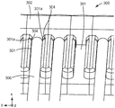
도 21 내지 도 23은 두 개의 별개의 섹션들(4110a 및 4110b)을 갖는 Y-홈(4110)을 도시한다. 도파관(4105)의 말단 단부(4103) 근처에서, 짧은 섹션에 종방향 전이 섹션(4115) 및 센터링 표면들(4126)이 포함된다. 도파관의 추가 축방향 이동은 도파관 정지부(604)에 의해 제한된다. 섹션(4110a)은 인덱스-매칭 접착제로 채워질 수 있다. 도파관(4105)의 정확한 각도 정렬을 제공하지만 접착제가 채워지지 않도록 섹션(4110b)으로부터 충분한 거리(예컨대, 0.5 mm)만큼 별개의 섹션(4110b)이 배치된다. 이 설계는 각도 정렬을 손상시키지 않도록 (본딩 길이를 최소화하여) 열팽창과 연관된 응력을 최소화한다.Figs. 21-23 illustrate a Y-
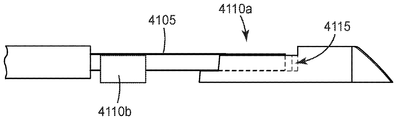
도 24는 다양한 실시예들에 따른 LCU(6100)의 일부분을 예시한다. 도 24에 도시된 LCU(6100)는 단일 LCU 부착 영역(6102)을 포함한다. 단일 LCU 부착 영역(6102)이 도 24에 도시되었지만, 다수의 광 도파관들을 수용하고 그에 영구적으로 부착되기 위해 다수의 부착 영역들(6102)이 LCU(6100) 상에 제공될 수 있음이 이해된다. LCU 부착 영역(6102)은 입구(6111) 및 말단 단부(6113)를 갖는 홈(6110)을 포함한다. 홈(6110)은 도 5에 도시된 일반적으로 원통형인 도파관(4105)과 같은 광 도파관을 수용하도록 구성된다.FIG. 24 illustrates a portion of an
LCU(6100)는 광 방향전환 부재(도 24에 도시되지 않았으나, 도 4의 4104 참조) 및 광 방향전환 부재와 말단 단부(6113) 사이의 중간 섹션(6108)을 포함한다. 일부 실시예들에서, 말단 단부(6113)는 렌즈와 같은 광학적으로 투명한 부재를 포함하거나 광학적으로 투명한 재료로 형성된다. 중간 섹션(6108)은 광학적으로 투명한 재료로 형성된다. 광 방향전환 부재는 출력 측면을 포함하며, 이를 통해 광이 광 유도 부재로부터 방출(또는 그 내부로 진입)된다.
일부 실시예들에 따라, 위에서 상세히 설명된 바와 같이, 홈(6110)은 일반적으로 U자형 하부 부분(6123) 및 확장된 상부 부분(6127, 6132)에 의해 형성된 복합 홈으로서 일반적으로 Y자형(Y-홈)인 복합 홈을 이룬다. 홈(6110)은 단일 센터링 측벽(6126)을 포함하는 종방향 전이 섹션(6115)을 포함한다. 종방향 전이 섹션(6115) 내에서, 측벽들(6122 및 6122') 사이의 간격은 광 도파관(6105)의 폭과 클리어런스의 합과 동일한 폭으로부터 광 도파관(6105)의 폭보다 작은 폭으로 감소한다. 도 24에 예시된 실시예에서, 측벽들(6122) 중 하나는 홈(6110)의 입구(6111)와 말단 단부(6113) 사이에서 실질적으로 평면이다. 대향 측벽(6122')은 측벽(6122)과 실질적으로 평행하고 전이 섹션(6115) 내에서 내향으로 각도를 이루는 센터링 측벽(6126)으로 전이하는 측벽 부분을 포함한다. 센터링 측벽(6126)은 홈(6110)의 모따기된 측벽으로 간주될 수 있다.According to some embodiments, as described in detail above, the
도 24에서, 홈(6110)은 홈(6110)의 일 측면 상에만 센터링 측벽(6126)을 포함한다. 이와 같이, 단일 센터링 측벽(6126)은 위치결정 측벽(6126)으로 간주될 수 있다. 조립 중에, 광 도파관(6105)은 도 24에 도시된 바와 같이, 위치결정 측벽(6126)이 광 도파관(6105)을 그의 홈(6110) 내의 도파관 정지부(604)의 위치에 핀고정(pin)할 때까지 평면 측벽(6122)을 따라 슬라이딩된다. 이 위치에서, 위치결정 측벽(6126)은 도파관 정지부(604)로서 기능하고, 홈(6110) 내에서 광 도파관(6105)의 말단 단부(6103)의 추가의 종방향 전진을 방지한다. 도 24에 도시된 실시예에 대한 하나의 이점은 조립 중에 광 도파관(6105)의 각도가 잘 제어될 수 있다는 것인데, 이는 그것이 측벽(6122)과 평행하게 절곡될 수 있기 때문이다. 일부 실시예들에서, 위치결정 측벽(6126)은 광 도파관(6105)을 핀치(pinch)할 필요가 없고, 대신 조립 중에 광 도파관(6105)이 측벽(6122)에 대해 절곡될 수 있는 한, 예컨대, 홈(6110)의 단부 또는 일부 다른 장벽을 정의함으로써 종래의 정지부로서 기능할 수 있다.In Fig. 24,
본 명세서에 기술된 접근법들과 함께 사용될 수 있는 페룰들, 정렬 프레임들 및 커넥터들에 관한 부가 정보는 본 명세서에 참고로 포함된 공동 소유이며 동시에 출원된 다음의 미국 특허 출원들에 제공된다: "Connector with Latching Mechanism"이라는 제목을 가지며, 대리인 사건 번호 제76663US002호로 식별된 미국 특허 출원 제62/239,998호; "Optical Ferrules"이라는 제목을 가지며 대리인 사건 번호 제76982US002호로 식별된 미국 특허 출원 제62/240,069호; "Ferrules, Alignment Frames and Connectors"라는 제목을 가지며 대리인 사건 번호 제75767US002호로 식별된 미국 특허 출원 제62/240,066호; "Optical Coupling Device with Waveguide Assisted Registration"라는 제목을 가지며 대리인 사건 번호 제76660US002호로 식별된 미국 특허 출원 제62/240,010호; "Optical Cable Assembly with Retainer"라는 제목을 가지며 대리인 사건 번호 제76662US002호로 식별된 미국 특허 출원 제62/240,008호; "Dust Mitigating Optical Connector"라는 제목을 가지며 대리인 사건 번호 제76664US002호로 식별된 미국 특허 출원 제62/240,000호; "Optical Waveguide Registration Feature"라는 제목을 가지며 대리인 사건 번호 제76661US002호로 식별된 미국 특허 출원 제62/240,009호; "Optical Ferrules and Optical Ferrule Molds"라는 제목을 가지며 대리인 사건 번호 제75985US002호로 식별된 미국 특허 출원 제62/239,996호; "Configurable Modular Connectors"라는 제목을 가지며 대리인 사건 번호 제76907US002호로 식별된 미국 특허 출원 제62/240,003호; "Hybrid Connectors"라는 제목을 가지며 대리인 사건 번호 제76908US002호로 식별된 미국 특허 출원 제62/240,005호.Additional information regarding ferrules, alignment frames, and connectors that may be used with the approaches described herein are provided in the following co-owned and co-pending U.S. patent applications, which are incorporated herein by reference: " Connector with Latching Mechanism ", U.S. Patent Application 62 / 239,998, identified as Attorney Docket No. 76663US002; U.S. Patent Application 62 / 240,069 entitled " Optical Ferrules " and identified as Attorney Docket No. 76982US002; U.S. Patent Application 62 / 240,066 entitled " Ferrules, Alignment Frames and Connectors "and identified as Attorney Docket No. 75767US002; U.S. Patent Application No. 62 / 240,010 entitled " Optical Coupling Device with Waveguide Assisted Registration "and identified as Attorney Docket No. 76660US002; U.S. Patent Application No. 62 / 240,008 entitled " Optical Cable Assembly with Retainer " and identified as Attorney Docket No. 76662US002; U.S. Patent Application 62 / 240,000 entitled " Dust Mitigating Optical Connector "and identified as Attorney Docket No. 76664US002; U.S. Patent Application No. 62 / 240,009 entitled " Optical Waveguide Registration Feature " and identified as Attorney Docket No. 76661US002; U.S. Patent Application No. 62 / 239,996 entitled " Optical Ferrules and Optical Ferrule Molds " and identified as Attorney Docket No. 75985US002; U.S. Patent Application No. 62 / 240,003 entitled " Configurable Modular Connectors " and identified as Attorney Docket No. 76907US002; U.S. Patent Application 62 / 240,005 entitled " Hybrid Connectors " and identified as Attorney Docket No. 76908US002.
본 발명에 설명된 항목들은 다음을 포함한다:The items described in the present invention include:
항목 1.
광학 페룰로서,
광이 광학 페룰 내에서 전파될 때, 광 도파관으로부터의 광의 하나 이상의 특성들에 영향을 미치도록 구성된 적어도 하나의 광 영향 요소 - 광 영향 요소는 입력 표면을 가짐 -;At least one optical influencing element configured to affect one or more characteristics of light from the optical waveguide when the light propagates in the optical ferrule, the optical affecting element having an input surface;
도파관의 출력 표면이 광 영향 요소의 입력 표면에 광학적으로 결합되도록 광 도파관을 수용하고 고정하도록 구성된 적어도 하나의 수용 요소;At least one receiving element configured to receive and fix the optical waveguide such that the output surface of the waveguide is optically coupled to the input surface of the optical influencing element;
광 도파관이 수용 요소 내에 설치되는 경우에, 광 영향 요소의 입력 표면을 향한 도파관의 이동을 제한하도록 구성된 도파관 정지부; 및A waveguide stop configured to limit movement of the waveguide toward the input surface of the light influencing element when the lightguide is installed in the receiving element; And
광 도파관의 출력 표면과 광 영향 요소의 입력 표면 사이의 공간 - 광 도파관이 수용 요소 내에 설치되는 경우에, 광 도파관은 공간에 접근불가능함- 을 포함하는, 광학 페룰.Wherein the optical waveguide is inaccessible to space when a space-light waveguide between the output surface of the optical waveguide and the input surface of the light influencing element is installed in the receiving element.
항목 2.
항목 1에 있어서, 수용 요소는 하나 이상의 홈들을 포함하는, 광학 페룰.Item 2.
The optical ferrule according to
항목 3.
항목 1에 있어서, 수용 요소는 하나 이상의 구멍들을 포함하는, 광학 페룰.Item 3.
The optical ferrule according to
항목 4.
항목 1에 있어서, 수용 요소는 적어도 하나의 원통형 구멍을 포함하는, 광학 페룰.Item 4.
The optical ferrule according to
항목 5.
항목 1 내지 항목 4 중 어느 한 항목에 있어서, 광학 페룰은 단일 광섬유 페룰인, 광학 페룰.Item 5.
4. The optical ferrule according to any one of
항목 6.
항목 1 내지 항목 4 중 어느 한 항목에 있어서, 광학 페룰은 다중 광섬유 페룰인, 광학 페룰.Item 6.
4. The optical ferrule according to any one of
항목 7.
항목 1에 있어서, 수용 요소는 U자형 홈인, 광학 페룰.Item 7.
항목 8. 항목 7에 있어서, 도파관 정지부는, U자형 홈의 폭이 도파관의 직경보다 작은 위치를 포함하는, 광학 페룰.Item 8. Item 7, wherein the waveguide stop includes a position where the width of the U-shaped groove is smaller than the diameter of the waveguide.
항목 9. 항목 7에 있어서, U자형 홈은 U자형 홈 내에 광 도파관을 중심설정하도록 구성된 센터링 측벽들을 포함하는, 광학 페룰.Item 9. Item 7. The optical ferrule according to item 7, wherein the U-shaped groove comprises centering sidewalls adapted to center the optical waveguide in the U-shaped groove.
항목 10. 항목 7에 있어서, U자형 홈은 U자형 홈 내에 광 도파관을 위치시키도록 구성된 적어도 하나의 센터링 측벽을 포함하는, 광학 페룰.Item 10. Item 7. The optical ferrule according to item 7, wherein the U-shaped groove includes at least one centering sidewall configured to position the optical waveguide in the U-shaped groove.
항목 11.
항목 1에 있어서, 수용 요소는 V자형 홈인, 광학 페룰.
항목 12.
항목 1에 있어서, 수용 요소는 Y자형 홈인, 광학 페룰.Item 12.
항목 13. 항목 12에 있어서, 도파관 정지부는, Y자형 홈의 폭이 도파관의 직경보다 작은 위치를 포함하는, 광학 페룰.Item 13. Item 12, wherein the waveguide stop includes a position where the width of the Y-shaped groove is smaller than the diameter of the waveguide.
항목 14. 항목 12에 있어서, Y자형 홈은 Y자형 홈 내에 광 도파관을 위치시키도록 구성된 하나 이상의 센터링 측벽들을 포함하는, 광학 페룰.Item 14. Item 12. The optical ferrule of Item 12, wherein the Y-shaped groove comprises one or more centering sidewalls configured to position the optical waveguide in the Y-shaped groove.
항목 15. 항목 12에 있어서, Y자형 홈은 Y자형 홈 내에 광 도파관을 위치시키도록 구성된 적어도 하나의 센터링 측벽을 포함하는, 광학 페룰.Item 15. Item 12. The optical ferrule of Item 12, wherein the Y-shaped groove includes at least one centering sidewall configured to position the optical waveguide in the Y-shaped groove.
항목 16. 항목 12에 있어서, 센터링 측벽들 사이의 폭은 입력 표면을 향한 방향으로 홈의 종축을 따라 점진적으로 좁아지는, 광학 페룰.Item 16. Item 12, wherein the width between the centering sidewalls progressively narrows along the longitudinal axis of the groove in the direction toward the input surface.
항목 17. 항목 16에 있어서, 도파관 정지부는, 센터링 측벽들 사이의 폭이 도파관의 직경보다 작은 위치를 포함하는, 광학 페룰.Item 17. Item 16, wherein the waveguide stop includes a position where the width between the centering sidewalls is smaller than the diameter of the waveguide.
항목 18.
항목 1 내지 항목 17 중 어느 한 항목에 있어서, 도파관 정지부는 벽을 포함하는, 광학 페룰.Item 18.
17. The optical ferrule according to any one of
항목 19.
항목 1 내지 항목 18 중 어느 한 항목에 있어서, 광 영향 요소는 렌즈를 포함하는, 광학 페룰.Item 19.
17. The optical ferrule according to any one of
항목 20.
항목 1 내지 항목 19 중 어느 한 항목에 있어서, 광 영향 요소는 광 도파관으로부터의 광을 방향전환하도록 구성된 요소를 포함하는, 광학 페룰.Item 20.
The optical ferrule as claimed in any of
항목 21.
항목 1 내지 항목 20 중 어느 한 항목에 있어서, 도파관 접근불가능 공간은 광이 도파관의 출력 표면과 광 영향 요소의 입력 표면 사이에서 방해 없이 전파되도록 구성되는, 광학 페룰.Item 21.
The optical ferrule as in any of
항목 22.
항목 1 내지 항목 21 중 어느 한 항목에 있어서, 도파관 접근불가능 공간은 접착제 저장소를 포함하는, 광학 페룰.Item 22.
The optical ferrule according to any one of
항목 23.
항목 1 내지 항목 22 중 어느 한 항목에 있어서, 도파관 접근불가능 공간은 유연성 재료를 포함하도록 구성되는, 광학 페룰.Item 23.
The optical ferrule according to any one of
항목 24. 항목 23에 있어서, 유연성 재료는 광학 접착제, 광학 젤, 및 광학 오일 중에 하나 이상인, 광학 페룰.Item 24. Item 23. The optical ferrule according to item 23, wherein the flexible material is at least one of an optical adhesive, an optical gel, and an optical oil.
항목 25.
항목 1 내지 항목 24 중 어느 한 항목에 있어서, 도파관의 출력 표면과 광 영향 요소의 입력 표면 사이의 거리는 약 10 μm 초과인, 광학 페룰.Item 25.
The optical ferrule as claimed in any of
항목 26.
항목 1 내지 항목 24 중 어느 한 항목에 있어서, 도파관의 출력 표면과 광 영향 요소의 입력 표면 사이의 거리는 약 40 μm 초과인, 광학 페룰.Item 26.
The optical ferrule as claimed in any of
항목 27. 항목 1 내지 항목 24 중 어느 한 항목에 있어서, 도파관 정지부는 도파관 정지부와 광 영향 요소의 입력 표면 사이의 거리가 약 10 μm 초과가 되도록 위치되는, 광학 페룰.Item 27. Item 24, wherein the waveguide stop is located such that the distance between the waveguide stop and the input surface of the light influencing element is greater than about 10 [mu] m.
항목 28. 항목 1 내지 항목 24 중 어느 한 항목에 있어서, 도파관 정지부는 도파관 정지부와 광 영향 요소의 입력 표면 사이의 거리가 약 40 μm 초과가 되도록 위치되는, 광학 페룰.Item 28. Item 24, wherein the waveguide stop is located such that the distance between the waveguide stop and the input surface of the light influencing element is greater than about 40 占 퐉.
항목 29.
항목 1 내지 항목 28 중 어느 한 항목에 있어서, 광 도파관은 접착제에 의해 수용 요소에 고정되는, 광학 페룰.Item 29.
The optical ferrule as described in any one of
항목 30.
항목 1 내지 항목 29 중 어느 한 항목에 있어서, 접착제는 광 도파관으로부터의 광에 대해 실질적으로 투명한, 광학 페룰.Item 30.
The optical ferrule as described in any one of
항목 31. 항목 29에 있어서, 접착제는 또한 접근불가능 공간 내에 배치되는, 광학 페룰.Item 31. Item 29. The optical ferrule according to item 29, wherein the adhesive is also disposed in the inaccessible space.
항목 32. 항목 29에 있어서, 광학적 투명 재료가 접근불가능 공간 내에 배치되는, 광학 페룰.Item 32. Item 29. The optical ferrule according to item 29, wherein the optical transparent material is disposed in the inaccessible space.
항목 33. 항목 32에 있어서, 광학적 투명 재료는 접착제와 상이한, 광학 페룰.Item 33. Item 32. The optical ferrule according to item 32, wherein the optical transparent material is different from the adhesive.
항목 34. 항목 29에 있어서, 접착제는 광 도파관으로부터의 광에 투명하지 않은, 광학 페룰.Item 34. Item 29. The optical ferrule according to item 29, wherein the adhesive is not transparent to light from the light pipe.
항목 35. 광학 페룰로서,Item 35. As the optical ferrule,
광 도파관을 수용하고 고정하도록 구성된 적어도 하나의 홈;At least one groove configured to receive and fix the light pipe;
광이 광학 페룰 내에서 전파될 때, 광 도파관으로부터의 광의 하나 이상의 특성들에 영향을 미치도록 구성된 적어도 하나의 광 영향 요소 - 광 영향 요소는 홈에 근접한 입력 표면을 가짐 -;At least one light influencing element configured to affect one or more properties of light from the light pipe when the light propagates in the optical ferrule, the light influencing element having an input surface proximate to the groove;
광 영향 요소의 입력 표면에 근접한 홈 내에 배치된 도파관 정지부 - 도파관 정지부는 입력 표면을 향한 광 도파관의 이동을 제한하도록 구성됨 -; 및A waveguide stop disposed in a groove proximate the input surface of the light influencing element, the waveguide stop being configured to limit movement of the optical waveguide towards the input surface; And
광 영향 요소의 입력 표면과 광 도파관의 출력 표면 사이의 공간 - 광 도파관이 홈 내에 설치되는 경우에, 광 도파관은 공간에 접근불가능함 - 을 포함하는, 광학 페룰.Wherein the optical waveguide is inaccessible to space when a space-light waveguide between the input surface of the light influencing element and the output surface of the optical waveguide is provided in the groove.
항목 36. 항목 35에 있어서, 홈은 U자형, V자형, 또는 Y자형 홈을 포함하는, 광학 페룰.Item 36. Item 35. The optical ferrule according to item 35, wherein the groove includes a U-shaped, V-shaped, or Y-shaped groove.
항목 37. 항목 35 또는 항목 36에 있어서, 홈은 홈 내에 광 도파관을 중심설정하도록 구성된 센터링 측벽들을 포함하는, 광학 페룰.Item 37. Item 35. The optical ferrule as in item 35 or 36, wherein the grooves include centering sidewalls configured to center the light pipe in the groove.
항목 38. 항목 37에 있어서, 도파관 정지부는, 센터링 측벽들 사이의 폭이 도파관의 직경보다 작은 위치를 포함하는, 광학 페룰.Item 38. Item 37. The optical ferrule according to item 37, wherein the waveguide stop includes a position where the width between the centering sidewalls is smaller than the diameter of the waveguide.
항목 39. 항목 35 내지 항목 38 중 어느 한 항목에 있어서, 광 영향 요소는 렌즈를 포함하는, 광학 페룰.Item 39. Item 35. The optical ferrule according to any one of items 35 to 38, wherein the light influencing element comprises a lens.
항목 40. 항목 35 내지 항목 39 중 어느 한 항목에 있어서, 광 영향 요소는 광 도파관으로부터의 광을 방향전환하도록 구성된 요소를 포함하는, 광학 페룰.Item 40. Item 35. The optical ferrule of any of items 35 to 39, wherein the light influencing element comprises an element configured to redirect light from the light pipe.
항목 41. 항목 35 내지 항목 40 중 어느 한 항목에 있어서, 도파관 접근불가능 공간은 유연성 재료를 포함하도록 구성된 저장소를 포함하는, 광학 페룰.Item 41. Item 35. The optical ferrule of any of items 35 to 40, wherein the waveguide inaccessible space comprises a reservoir configured to contain a flexible material.
항목 42. 항목 35 내지 항목 41 중 어느 한 항목에 있어서, 도파관 접근불가능 공간은, 접착제로 채워지는 경우에, 도파관의 출력 표면과 광 영향 요소의 입력 표면 사이에서 광이 실질적으로 방해 없이 전파되도록 구성되는, 광학 페룰.Item 42. Item 35. The method of any one of items 35 to 41, wherein the waveguide inaccessible space is configured such that, when filled with an adhesive, the light is transmitted between the output surface of the waveguide and the input surface of the light influencing element substantially without interference. Ferrules.
항목 43. 항목 35 내지 항목 42 중 어느 한 항목에 있어서, 도파관 정지부는 도파관의 출력 표면과 광 영향 요소의 입력 표면 사이의 거리가 약 10 μm 초과가 되도록 위치되는, 광학 페룰.Item 43. Item 35. The optical ferrule as claimed in any of items 35 to 42, wherein the waveguide stop is positioned such that the distance between the output surface of the waveguide and the input surface of the light influencing element is greater than about 10 占 퐉.
항목 44. 항목 35 내지 항목 42 중 어느 한 항목에 있어서, 도파관 정지부는 도파관의 출력 표면과 광 영향 요소의 입력 표면 사이의 거리가 약 40 μm 초과가 되도록 위치되는, 광학 페룰.Item 44. Item 35. The optical ferrule of any of items 35 to 42, wherein the waveguide stop is positioned such that the distance between the output surface of the waveguide and the input surface of the light influencing element is greater than about 40 占 퐉.
항목 45. 항목 35 내지 항목 42 중 어느 한 항목에 있어서, 도파관 정지부와 광 영향 요소의 입력 표면 사이의 거리는 약 10 μm 초과인, 광학 페룰.Item 45. Item 35. The optical ferrule as claimed in any of items 35 to 42, wherein the distance between the waveguide stop and the input surface of the light influencing element is greater than about 10 占 퐉.
항목 46. 항목 35 내지 항목 42 중 어느 한 항목에 있어서, 도파관 정지부와 광 영향 요소의 입력 표면 사이의 거리는 약 40 μm 초과인, 광학 페룰.Item 46. Item 35. The optical ferrule as claimed in any of items 35 to 42, wherein the distance between the waveguide stop and the input surface of the light influencing element is greater than about 40 占 퐉.
항목 47. 항목 35 내지 항목 46 중 어느 한 항목에 있어서, 홈은 측벽들을 포함하며, 전이 섹션의 측벽들 사이의 간격은 광 영향 요소의 입력 표면을 향해 홈을 따라 감소하는, 광학 페룰.Item 47. Item 35. The optical ferrule of any of items 35 to 46, wherein the grooves include sidewalls, the spacing between the sidewalls of the transition section decreasing along the grooves towards the input surface of the light influencing element.
항목 48. 항목 47에 있어서, 전이 섹션은 실질적으로 평면 측벽들을 포함하는, 광학 페룰.Item 48. Item 47. The optical ferrule of Item 47, wherein the transition section comprises substantially planar sidewalls.
항목 49. 항목 47에 있어서, 전이 섹션은 비-평면 측벽들을 포함하는, 광학 페룰.Item 49. Item 47. The optical ferrule of item 47, wherein the transition section comprises non-planar side walls.
항목 50. 항목 47에 있어서, 광 도파관의 출력 표면은 도파관 정지부에서 전이 섹션의 측벽들과 접촉하는, 광학 페룰.Item 50. Item 47. The optical ferrule of item 47, wherein the output surface of the optical waveguide contacts the sidewalls of the transition section at the waveguide stop.
항목 51. 항목 47에 있어서, 광 도파관의 클래딩과 전이 섹션의 측벽들 사이의 접촉은 광 도파관을 홈의 중심 평면으로 측방향으로 가이드하는, 광학 페룰.Item 51. Item 47, wherein the contact between the cladding of the optical waveguide and the side walls of the transition section guides the optical waveguide to the center plane of the groove in the lateral direction.
항목 52. 항목 35 내지 항목 51 중 어느 한 항목에 있어서, 도파관은 단일-모드 또는 다중-모드 광섬유인, 광학 페룰.Item 52. Item 35. The optical ferrule according to any one of items 35 to 51, wherein the waveguide is a single-mode or multi-mode optical fiber.
항목 53. 항목 35 내지 항목 52 중 어느 한 항목에 있어서, 각각의 홈의 저부 표면은 적어도 하나의 리세스된 섹션을 포함하는, 광학 페룰.Item 53. Item 35. The optical ferrule as in any of items 35 to 52, wherein the bottom surface of each groove comprises at least one recessed section.
항목 54. 항목 53에 있어서, 저부 표면의 대부분은 리세스된 섹션을 포함하는, 광학 페룰.Item 54. Item 53, wherein the majority of the bottom surface comprises a recessed section.
항목 55. 항목 35에 있어서, 도파관은 입력 표면을 향한 광 도파관의 이동을 제한하도록 도파관 정지부에 연결된 돌출 특징부를 포함하는, 광학 페룰.Item 55. Item 35. The optical ferrule according to item 35, wherein the waveguide comprises a protruding feature connected to the waveguide stop to limit movement of the optical waveguide towards the input surface.
달리 지시되지 않는 한, 본 명세서 및 청구범위에 사용되는 특징부 크기, 양, 및 물리적 특성을 표현하는 모든 수는 모든 경우에 용어 "약"에 의해 수식되는 것으로 이해되어야 한다. 따라서, 반대로 지시되지 않는 한, 전술한 명세서 및 첨부된 청구범위에 기재된 수치 파라미터는 본 명세서에 개시된 교시를 이용하는 당업자가 얻고자 하는 원하는 특성에 따라 달라질 수 있는 근사치이다. 종점(endpoint)에 의한 수치 범위의 사용은 그 범위 내의 모든 수(예컨대, 1 내지 5는 1, 1.5, 2, 2.75, 3, 3.80, 4 및 5를 포함함) 및 그 범위 내의 임의의 범위를 포함한다.Unless otherwise indicated, all numbers expressing feature sizes, amounts, and physical characteristics used in the present specification and claims are to be understood as being modified in all instances by the term "about ". Accordingly, unless indicated to the contrary, the numerical parameters set forth in the foregoing specification and attached claims are approximations that may vary depending upon the desired properties sought to be obtained by those skilled in the art using the teachings disclosed herein. The use of numerical ranges by endpoints means that any number within that range (e.g., 1 to 5 includes 1, 1.5, 2, 2.75, 3, 3.80, 4, and 5) .
위에서 논의된 일부 실시예들의 다양한 변형 및 변경은 당업자에게 명백할 것이고, 본 발명이 본 명세서에 기재된 예시적인 실시예들로 제한되지 않음이 이해되어야 한다. 독자는, 달리 지시되지 않는 한, 하나의 개시된 일부 실시예들의 특징부들은 또한 다른 모든 개시된 실시예에 적용될 수 있다고 생각하여야 한다. 또한, 본 명세서에서 언급된 모든 미국 특허, 특허 출원, 특허 출원 공보, 및 다른 특허와 비-특허 문헌이 전술한 개시 내용과 모순되지 않는 정도로 참고로 포함된다는 것을 이해하여야 한다.It should be understood that various changes and modifications to some of the embodiments discussed above will be apparent to those skilled in the art, and that the present invention is not limited to the exemplary embodiments described herein. The reader should be aware that, unless otherwise indicated, the features of some of the disclosed embodiments may also be applied to all other disclosed embodiments. It should also be understood that all US patents, patent applications, patent application publications, and other patents and non-patent documents referred to herein are incorporated by reference to the extent not inconsistent with the foregoing disclosure.
Claims (10)
광이 광학 페룰 내에서 전파될 때, 광 도파관으로부터의 광의 하나 이상의 특성들에 영향을 미치도록 구성된 적어도 하나의 광 영향 요소(light affecting element) - 광 영향 요소는 입력 표면을 가짐 -;
도파관의 출력 표면이 광 영향 요소의 입력 표면에 광학적으로 결합되도록 광 도파관을 수용하고 고정하도록 구성된 적어도 하나의 수용 요소;
광 도파관이 수용 요소 내에 설치되는 경우에, 광 영향 요소의 입력 표면을 향한 도파관의 이동을 제한하도록 구성된 도파관 정지부; 및
광 도파관의 출력 표면과 광 영향 요소의 입력 표면 사이의 공간 - 광 도파관이 수용 요소 내에 설치되는 경우에, 광 도파관은 공간에 접근불가능함- 을 포함하는, 광학 페룰.As an optical ferrule,
At least one light affecting element configured to affect one or more characteristics of light from the light pipe when the light propagates in the optical ferrule, the light affecting element having an input surface;
At least one receiving element configured to receive and fix the optical waveguide such that the output surface of the waveguide is optically coupled to the input surface of the optical influencing element;
A waveguide stop configured to limit movement of the waveguide toward the input surface of the light influencing element when the lightguide is installed in the receiving element; And
Wherein the optical waveguide is inaccessible to space when a space-light waveguide between the output surface of the optical waveguide and the input surface of the light influencing element is installed in the receiving element.
광 도파관을 수용하고 고정하도록 구성된 적어도 하나의 홈;
광이 광학 페룰 내에서 전파될 때, 광 도파관으로부터의 광의 하나 이상의 특성들에 영향을 미치도록 구성된 적어도 하나의 광 영향 요소 - 광 영향 요소는 홈에 근접한 입력 표면을 가짐 -;
광 영향 요소의 입력 표면에 근접한 홈 내에 배치된 도파관 정지부 - 도파관 정지부는 입력 표면을 향한 광 도파관의 이동을 제한하도록 구성됨 -; 및
광 영향 요소의 입력 표면과 광 도파관의 출력 표면 사이의 공간 - 광 도파관이 홈 내에 설치되는 경우에, 광 도파관은 공간에 접근불가능함 - 을 포함하는, 광학 페룰.As the optical ferrule,
At least one groove configured to receive and fix the light pipe;
At least one light influencing element configured to affect one or more properties of light from the light pipe when the light propagates in the optical ferrule, the light influencing element having an input surface proximate to the groove;
A waveguide stop disposed in a groove proximate the input surface of the light influencing element, the waveguide stop being configured to limit movement of the optical waveguide towards the input surface; And
Wherein the optical waveguide is inaccessible to space when a space-light waveguide between the input surface of the light influencing element and the output surface of the optical waveguide is provided in the groove.
Applications Claiming Priority (3)
| Application Number | Priority Date | Filing Date | Title |
|---|---|---|---|
| US201562240002P | 2015-10-12 | 2015-10-12 | |
| US62/240,002 | 2015-10-12 | ||
| PCT/US2016/055115 WO2017066018A1 (en) | 2015-10-12 | 2016-10-03 | Optical ferrules with waveguide inaccessible space |
Publications (1)
| Publication Number | Publication Date |
|---|---|
| KR20180064509A true KR20180064509A (en) | 2018-06-14 |
Family
ID=57138163
Family Applications (1)
| Application Number | Title | Priority Date | Filing Date |
|---|---|---|---|
| KR1020187013156A KR20180064509A (en) | 2015-10-12 | 2016-10-03 | Optical ferrules with waveguide inaccessible space |
Country Status (5)
| Country | Link |
|---|---|
| US (2) | US11307362B2 (en) |
| JP (2) | JP6952041B2 (en) |
| KR (1) | KR20180064509A (en) |
| CN (2) | CN108139549A (en) |
| WO (1) | WO2017066018A1 (en) |
Families Citing this family (12)
| Publication number | Priority date | Publication date | Assignee | Title |
|---|---|---|---|---|
| KR20180061365A (en) | 2015-10-12 | 2018-06-07 | 쓰리엠 이노베이티브 프로퍼티즈 컴파니 | Connector with latching mechanism |
| KR20180067578A (en) | 2015-10-12 | 2018-06-20 | 쓰리엠 이노베이티브 프로퍼티즈 컴파니 | Dust Reduction Fiber Connector |
| KR20180067580A (en) | 2015-10-12 | 2018-06-20 | 쓰리엠 이노베이티브 프로퍼티즈 컴파니 | Optical coupling device with waveguide auxiliary matching |
| CN108139547B (en) * | 2015-10-12 | 2020-09-08 | 3M创新有限公司 | Optical waveguide positioning features in a multi-waveguide connector |
| US11086083B2 (en) | 2015-12-30 | 2021-08-10 | 3M Innovative Properties Company | Optical connector with dust ingress mitigating cover |
| WO2020003124A1 (en) * | 2018-06-28 | 2020-01-02 | 3M Innovative Properties Company | Light coupling element and assembly |
| WO2020003245A1 (en) | 2018-06-29 | 2020-01-02 | 3M Innovative Properties Company | Optical ferrule |
| US11906793B2 (en) | 2019-03-26 | 2024-02-20 | 3M Innovative Properties Company | Optical connector assembly |
| US11726266B2 (en) | 2019-06-28 | 2023-08-15 | 3M Innovative Properties Company | Structured surface and optical ferrule including same |
| WO2021214575A1 (en) * | 2020-04-22 | 2021-10-28 | 3M Innovative Properties Company | Optical ferrules |
| WO2022172107A1 (en) * | 2021-02-11 | 2022-08-18 | 3M Innovative Properties Company | Optical connector and optical interconnect assembly |
| US11726268B1 (en) * | 2022-03-25 | 2023-08-15 | Enplas Corporation | Ferrule, optical connector, and optical connector module |
Family Cites Families (52)
| Publication number | Priority date | Publication date | Assignee | Title |
|---|---|---|---|---|
| US4718744A (en) * | 1985-08-16 | 1988-01-12 | Amp Incorporated | Collimating lens and holder for an optical fiber |
| US5257336A (en) * | 1992-08-21 | 1993-10-26 | At&T Bell Laboratories | Optical subassembly with passive optical alignment |
| JPH07120642A (en) * | 1993-10-21 | 1995-05-12 | Mitsubishi Rayon Co Ltd | Optical fiber type photoelectric switch attachment |
| US5706371A (en) | 1996-12-03 | 1998-01-06 | E-Tek Dynamics, Inc. | Optical isolator array device |
| JP2004157558A (en) * | 1997-06-25 | 2004-06-03 | Matsushita Electric Ind Co Ltd | Optical semiconductor module |
| US6332719B1 (en) | 1997-06-25 | 2001-12-25 | Matsushita Electric Industrial Co., Ltd. | Optical transmitter/receiver apparatus, method for fabricating the same and optical semiconductor module |
| JPH11211933A (en) * | 1998-01-23 | 1999-08-06 | Oki Electric Ind Co Ltd | Optical circuit/optical fiber connecting method |
| JP4019538B2 (en) * | 1998-03-16 | 2007-12-12 | 住友電気工業株式会社 | Optical module substrate and optical module |
| JP3775069B2 (en) * | 1998-09-18 | 2006-05-17 | 住友電気工業株式会社 | Optical receiver module |
| CA2282612A1 (en) | 1998-09-18 | 2000-03-18 | Sumitomo Electric Industries, Ltd. | Photodiode module |
| DE19934184A1 (en) * | 1999-07-21 | 2001-01-25 | Siemens Ag | Optical waveguide end-faces light coupling device e.g. for light-guide chip |
| DE19934178A1 (en) * | 1999-07-21 | 2001-01-25 | Siemens Ag | Optical coupler for coupling light from first optical fibre into second optical fibre guarantees improved guidance of variable-length element parallel to primary axis, preventing additional effort |
| US6168319B1 (en) * | 1999-08-05 | 2001-01-02 | Corning Incorporated | System and method for aligning optical fiber collimators |
| JP4096469B2 (en) * | 1999-09-09 | 2008-06-04 | 株式会社デンソー | Optical receiver module and method of manufacturing optical receiver module |
| JP2002357737A (en) * | 2001-05-31 | 2002-12-13 | Omron Corp | Optical communication component and method for manufacturing the same |
| JP4007118B2 (en) * | 2002-08-12 | 2007-11-14 | 住友電気工業株式会社 | Light emitting device, optical module, and grating chip |
| JP2004317627A (en) | 2003-04-14 | 2004-11-11 | Fujikura Ltd | Mount, optical module and transmitting and receiving module |
| DE112004000724B4 (en) | 2003-04-30 | 2021-08-05 | Fujikura Ltd. | Optical transceiver |
| CN1781043B (en) * | 2003-04-30 | 2011-05-11 | 株式会社藤仓 | Optical transceiver and optical connector |
| JP4515141B2 (en) * | 2003-04-30 | 2010-07-28 | 株式会社フジクラ | Optical transceiver |
| JP3865137B2 (en) * | 2003-04-30 | 2007-01-10 | 株式会社フジクラ | Optical connector |
| JP2005202229A (en) * | 2004-01-16 | 2005-07-28 | Fuji Xerox Co Ltd | Optical module |
| EP1866687A1 (en) * | 2005-04-04 | 2007-12-19 | Molex Incorporated | Multifiber mt-type connector and ferrule comprising v-groove lens array and method of manufacture |
| JP4116017B2 (en) | 2005-05-25 | 2008-07-09 | 株式会社フジクラ | Optical connector |
| JP2008151843A (en) * | 2006-12-14 | 2008-07-03 | Omron Corp | Optical component for optical transmission and method of manufacturing same |
| JP4903120B2 (en) | 2007-10-03 | 2012-03-28 | 株式会社フジクラ | Optical path changing member |
| US7726885B2 (en) | 2007-10-29 | 2010-06-01 | Fujikura Ltd. | Optical connector having a fitting protrusion or fitting recess used for positioning |
| JP2011095295A (en) * | 2009-10-27 | 2011-05-12 | Panasonic Electric Works Co Ltd | Optical fiber block of optical module and method of manufacturing the same |
| JP5564344B2 (en) | 2010-06-29 | 2014-07-30 | 株式会社フジクラ | Ferrule with optical fiber |
| JP2012047943A (en) * | 2010-08-26 | 2012-03-08 | Enplas Corp | Optical fiber holding member |
| JP2013057720A (en) * | 2011-09-07 | 2013-03-28 | Panasonic Corp | Optical module |
| WO2012176409A1 (en) * | 2011-06-22 | 2012-12-27 | パナソニック株式会社 | Optical module |
| JP5919573B2 (en) | 2011-09-07 | 2016-05-18 | パナソニックIpマネジメント株式会社 | Optical module |
| JP6011958B2 (en) * | 2012-03-28 | 2016-10-25 | 株式会社エンプラス | Optical receptacle and optical module having the same |
| JP2014026153A (en) * | 2012-07-27 | 2014-02-06 | Mitsubishi Pencil Co Ltd | Optical coupling member and optical connector using the same |
| FR2996011B1 (en) | 2012-09-21 | 2016-01-01 | Centre Nat Rech Scient | METHOD FOR CONNECTING OPTICAL FIBER AND CONNECTOR FOR OPTICAL FIBER |
| US10514512B2 (en) | 2012-10-05 | 2019-12-24 | 3M Innovative Properties Company | Optical connector |
| CN105026972B (en) | 2012-10-05 | 2017-07-07 | 3M创新有限公司 | Optical conenctor |
| TWI565989B (en) * | 2012-12-14 | 2017-01-11 | 鴻海精密工業股份有限公司 | Optical fiber connector |
| JP6034256B2 (en) * | 2013-07-04 | 2016-11-30 | 古河電気工業株式会社 | Optical fiber module and manufacturing method thereof |
| CN105556363B (en) | 2013-09-16 | 2017-06-30 | 3M创新有限公司 | Optical communication module |
| JP6410551B2 (en) | 2014-10-17 | 2018-10-24 | 古河電気工業株式会社 | Ferrule, optical fiber core wire with ferrule, manufacturing method of ferrule, and manufacturing method of optical fiber core wire with ferrule |
| WO2017066135A1 (en) | 2015-10-12 | 2017-04-20 | 3M Innovative Properties Company | Optical ferrules and optical ferrule molds |
| KR20180067580A (en) | 2015-10-12 | 2018-06-20 | 쓰리엠 이노베이티브 프로퍼티즈 컴파니 | Optical coupling device with waveguide auxiliary matching |
| KR20180061365A (en) | 2015-10-12 | 2018-06-07 | 쓰리엠 이노베이티브 프로퍼티즈 컴파니 | Connector with latching mechanism |
| CN108139551B (en) | 2015-10-12 | 2022-05-17 | 3M创新有限公司 | Hybrid connector |
| WO2017066037A1 (en) | 2015-10-12 | 2017-04-20 | 3M Innovative Properties Company | Optical ferrules |
| KR20180067578A (en) | 2015-10-12 | 2018-06-20 | 쓰리엠 이노베이티브 프로퍼티즈 컴파니 | Dust Reduction Fiber Connector |
| WO2017065999A2 (en) | 2015-10-12 | 2017-04-20 | 3M Innovative Properties Company | Ferrules, alignment frames and connectors |
| TW201728933A (en) | 2015-10-12 | 2017-08-16 | 3M新設資產公司 | Optical assembly with cable retainer |
| CN108139544B (en) | 2015-10-12 | 2020-08-07 | 3M创新有限公司 | Configurable modular connector |
| CN108139547B (en) | 2015-10-12 | 2020-09-08 | 3M创新有限公司 | Optical waveguide positioning features in a multi-waveguide connector |
-
2016
- 2016-10-03 US US15/763,526 patent/US11307362B2/en active Active
- 2016-10-03 CN CN201680059566.9A patent/CN108139549A/en active Pending
- 2016-10-03 KR KR1020187013156A patent/KR20180064509A/en unknown
- 2016-10-03 CN CN202210649429.8A patent/CN115079349A/en active Pending
- 2016-10-03 JP JP2018538045A patent/JP6952041B2/en active Active
- 2016-10-03 WO PCT/US2016/055115 patent/WO2017066018A1/en active Application Filing
-
2021
- 2021-06-23 JP JP2021103718A patent/JP7282128B2/en active Active
-
2022
- 2022-03-14 US US17/693,991 patent/US11880072B2/en active Active
Also Published As
| Publication number | Publication date |
|---|---|
| CN108139549A (en) | 2018-06-08 |
| JP2018530013A (en) | 2018-10-11 |
| US11307362B2 (en) | 2022-04-19 |
| JP2021157194A (en) | 2021-10-07 |
| WO2017066018A1 (en) | 2017-04-20 |
| US20190049671A1 (en) | 2019-02-14 |
| CN115079349A (en) | 2022-09-20 |
| US20220196925A1 (en) | 2022-06-23 |
| JP7282128B2 (en) | 2023-05-26 |
| US11880072B2 (en) | 2024-01-23 |
| JP6952041B2 (en) | 2021-10-20 |
Similar Documents
| Publication | Publication Date | Title |
|---|---|---|
| US11880072B2 (en) | Optical ferrules with waveguide inaccessible space | |
| US11874510B2 (en) | Optical assembly with cable retainer | |
| US11906789B2 (en) | Optical waveguide positioning feature in a multiple waveguides connector | |
| US11934019B2 (en) | Dust mitigating optical connector | |
| US7410303B2 (en) | Method and metal mold for manufacturing optical connector ferrule, optical connector ferrule manufactured by using the method, and optical connector and optical wiring system using the ferrule | |
| JP5734709B2 (en) | Optical connector and electronic information device | |
| TWI654456B (en) | Waveguide termination module and termination method | |
| EP3783408B1 (en) | Field installable rugged optical terminus | |
| JP2005309367A (en) | Optical fiber connector, optical fiber connecting body and connecting method | |
| WO2019077681A1 (en) | Ferrule, ferrule equipped with optical fibre, and method for producing ferrule |