JP6952041B2 - Optical ferrule with waveguide inaccessible space - Google Patents
Optical ferrule with waveguide inaccessible space Download PDFInfo
- Publication number
- JP6952041B2 JP6952041B2 JP2018538045A JP2018538045A JP6952041B2 JP 6952041 B2 JP6952041 B2 JP 6952041B2 JP 2018538045 A JP2018538045 A JP 2018538045A JP 2018538045 A JP2018538045 A JP 2018538045A JP 6952041 B2 JP6952041 B2 JP 6952041B2
- Authority
- JP
- Japan
- Prior art keywords
- waveguide
- optical
- groove
- light
- optical waveguide
- Prior art date
- Legal status (The legal status is an assumption and is not a legal conclusion. Google has not performed a legal analysis and makes no representation as to the accuracy of the status listed.)
- Active
Links
Images


Classifications
-
- G—PHYSICS
- G02—OPTICS
- G02B—OPTICAL ELEMENTS, SYSTEMS OR APPARATUS
- G02B6/00—Light guides; Structural details of arrangements comprising light guides and other optical elements, e.g. couplings
- G02B6/24—Coupling light guides
- G02B6/36—Mechanical coupling means
- G02B6/38—Mechanical coupling means having fibre to fibre mating means
- G02B6/3807—Dismountable connectors, i.e. comprising plugs
- G02B6/3833—Details of mounting fibres in ferrules; Assembly methods; Manufacture
- G02B6/3834—Means for centering or aligning the light guide within the ferrule
- G02B6/3838—Means for centering or aligning the light guide within the ferrule using grooves for light guides
- G02B6/3839—Means for centering or aligning the light guide within the ferrule using grooves for light guides for a plurality of light guides
-
- G—PHYSICS
- G02—OPTICS
- G02B—OPTICAL ELEMENTS, SYSTEMS OR APPARATUS
- G02B6/00—Light guides; Structural details of arrangements comprising light guides and other optical elements, e.g. couplings
- G02B6/24—Coupling light guides
- G02B6/36—Mechanical coupling means
- G02B6/38—Mechanical coupling means having fibre to fibre mating means
- G02B6/3807—Dismountable connectors, i.e. comprising plugs
- G02B6/381—Dismountable connectors, i.e. comprising plugs of the ferrule type, e.g. fibre ends embedded in ferrules, connecting a pair of fibres
- G02B6/3818—Dismountable connectors, i.e. comprising plugs of the ferrule type, e.g. fibre ends embedded in ferrules, connecting a pair of fibres of a low-reflection-loss type
- G02B6/382—Dismountable connectors, i.e. comprising plugs of the ferrule type, e.g. fibre ends embedded in ferrules, connecting a pair of fibres of a low-reflection-loss type with index-matching medium between light guides
-
- G—PHYSICS
- G02—OPTICS
- G02B—OPTICAL ELEMENTS, SYSTEMS OR APPARATUS
- G02B6/00—Light guides; Structural details of arrangements comprising light guides and other optical elements, e.g. couplings
- G02B6/24—Coupling light guides
- G02B6/36—Mechanical coupling means
- G02B6/38—Mechanical coupling means having fibre to fibre mating means
- G02B6/3807—Dismountable connectors, i.e. comprising plugs
- G02B6/3833—Details of mounting fibres in ferrules; Assembly methods; Manufacture
- G02B6/3834—Means for centering or aligning the light guide within the ferrule
- G02B6/3838—Means for centering or aligning the light guide within the ferrule using grooves for light guides
-
- G—PHYSICS
- G02—OPTICS
- G02B—OPTICAL ELEMENTS, SYSTEMS OR APPARATUS
- G02B6/00—Light guides; Structural details of arrangements comprising light guides and other optical elements, e.g. couplings
- G02B6/24—Coupling light guides
- G02B6/36—Mechanical coupling means
- G02B6/38—Mechanical coupling means having fibre to fibre mating means
- G02B6/3807—Dismountable connectors, i.e. comprising plugs
- G02B6/3833—Details of mounting fibres in ferrules; Assembly methods; Manufacture
- G02B6/3853—Lens inside the ferrule
-
- G—PHYSICS
- G02—OPTICS
- G02B—OPTICAL ELEMENTS, SYSTEMS OR APPARATUS
- G02B6/00—Light guides; Structural details of arrangements comprising light guides and other optical elements, e.g. couplings
- G02B6/24—Coupling light guides
- G02B6/36—Mechanical coupling means
- G02B6/38—Mechanical coupling means having fibre to fibre mating means
- G02B6/3807—Dismountable connectors, i.e. comprising plugs
- G02B6/3833—Details of mounting fibres in ferrules; Assembly methods; Manufacture
- G02B6/3855—Details of mounting fibres in ferrules; Assembly methods; Manufacture characterised by the method of anchoring or fixing the fibre within the ferrule
- G02B6/3861—Adhesive bonding
-
- G—PHYSICS
- G02—OPTICS
- G02B—OPTICAL ELEMENTS, SYSTEMS OR APPARATUS
- G02B6/00—Light guides; Structural details of arrangements comprising light guides and other optical elements, e.g. couplings
- G02B6/24—Coupling light guides
- G02B6/36—Mechanical coupling means
- G02B6/38—Mechanical coupling means having fibre to fibre mating means
- G02B6/3807—Dismountable connectors, i.e. comprising plugs
- G02B6/3873—Connectors using guide surfaces for aligning ferrule ends, e.g. tubes, sleeves, V-grooves, rods, pins, balls
- G02B6/3885—Multicore or multichannel optical connectors, i.e. one single ferrule containing more than one fibre, e.g. ribbon type
-
- G—PHYSICS
- G02—OPTICS
- G02B—OPTICAL ELEMENTS, SYSTEMS OR APPARATUS
- G02B6/00—Light guides; Structural details of arrangements comprising light guides and other optical elements, e.g. couplings
- G02B6/24—Coupling light guides
- G02B6/36—Mechanical coupling means
- G02B6/3628—Mechanical coupling means for mounting fibres to supporting carriers
- G02B6/3648—Supporting carriers of a microbench type, i.e. with micromachined additional mechanical structures
- G02B6/3652—Supporting carriers of a microbench type, i.e. with micromachined additional mechanical structures the additional structures being prepositioning mounting areas, allowing only movement in one dimension, e.g. grooves, trenches or vias in the microbench surface, i.e. self aligning supporting carriers
Description
本開示は、全般的に、光フェルールなどの光結合装置に関する。 The present disclosure generally relates to optical coupling devices such as optical ferrules.
光フェルールは、1つ以上の導波路からの光が、第1のフェルールを経て、接続相手の第2のフェルールの、対応する導波路又は他の装置のセットへと通過することを可能にする。それらの光フェルールは、機械的に一体に結合して、その第1の装置の光学素子と、接続相手の装置の光学素子とを、位置合わせすることができる。光フェルールは、電気通信ネットワーク、ローカルエリアネットワーク、データセンターリンク、及び、コンピュータ装置内の内部リンクを含めた、様々な用途における光通信のために使用される。 Optical ferrules allow light from one or more waveguides to pass through a first ferrule to a corresponding set of waveguides or other equipment of a second ferrule to connect to. .. These optical ferrules can be mechanically integrally coupled to align the optical element of the first device with the optical element of the device to be connected. Optical ferrules are used for optical communications in a variety of applications, including telecommunications networks, local area networks, data center links, and internal links within computer equipment.
一部の実施形態は、光フェルールに関与するものであり、この光フェルールは、光導波路からの光が光フェルール内で伝播する際に、その光の1つ以上の特性に影響を及ぼすように構成されている、少なくとも1つの光影響要素を含み、この光影響要素は、入力面を有する。少なくとも1つの受け入れ要素が、光導波路を受け入れて固定することにより、光影響要素の入力面に、その導波路の出力面が光学的に結合される。受け入れ要素内に光導波路が装着された際に、導波路停止部が、光影響要素の入力面に向けた、その導波路の移動を制限する。光導波路の出力面と光影響要素の入力面との間のスペースは、受け入れ要素内に光導波路が装着された際に、その光導波路にはアクセス不可能なものである。 Some embodiments involve an optical ferrule, such that the optical ferrule affects one or more properties of the light as it propagates within the optical waveguide. Containing at least one light-affected element that is constructed, this light-affected element has an input surface. By accepting and fixing the optical waveguide at least one receiving element, the output surface of the waveguide is optically coupled to the input surface of the optical waveguide. When the optical waveguide is mounted within the receiving element, the waveguide stop limits the movement of the waveguide towards the input surface of the light-affected element. The space between the output surface of the optical waveguide and the input surface of the optical waveguide is inaccessible to the optical waveguide when it is mounted within the receiving element.
一部の実施形態は、光導波路を受け入れて固定するように構成された、少なくとも1つの溝を含む、光フェルールを目的とする。少なくとも1つの光影響要素が、光導波路からの光が光フェルール内で伝播する際に、その光の1つ以上の特性に影響を及ぼすように構成されており、この光影響要素は、溝の近位に入力面を有する。光影響要素の入力面の近位で溝内に配設されている、導波路停止部が、その入力面に向けた光導波路の動きを制限する。光影響要素の入力面と光導波路の出力面との間のスペースは、溝内に光導波路が装着された際に、その光導波路にはアクセス不可能なものである。 Some embodiments are intended for optical ferrules that include at least one groove configured to receive and secure an optical waveguide. At least one light-influencing element is configured to affect one or more properties of the light as the light from the optical waveguide propagates within the optical waveguide, and the light-influencing element is a groove. It has an input surface proximal to it. A waveguide stop located in the groove proximal to the input surface of the light-affecting element limits the movement of the optical waveguide towards the input surface. The space between the input surface of the optical influence element and the output surface of the optical waveguide is inaccessible to the optical waveguide when the optical waveguide is mounted in the groove.
これらの図は、必ずしも一定の比率の縮尺ではない。図中で使用される同様の数字は、同様の構成要素を指す。しかしながら、所与の図中での、ある構成要素を指すある数字の使用は、同じ数字が付された別の図中の構成要素を限定することを意図するものではない点が理解されるであろう。 These figures are not necessarily at a constant scale. Similar numbers used in the figures refer to similar components. However, it is understood that the use of a number to refer to one component in a given figure is not intended to limit the component in another figure with the same number. There will be.
ポリマー光フェルールなどの光フェルールに、屈折率整合接着剤を使用して、ガラス光ファイバが取り付けられる場合、そのファイバの先端から、及び/又は、そのフェルールの光影響要素の光入力面から、接着剤が剥離するという問題が生じる恐れがある。これらのシステムにおいて典型的には、ファイバは、光入力面と接触するように押し込まれ、そのファイバ先端と光影響要素の入力面との間に、極めて薄い接着剤の層が残される。熱膨張差、接着剤の収縮、及び/又は機械的力が、この界面に応力を加えることにより、接着破壊が引き起こされる恐れがある。 When a glass optical fiber is attached to an optical ferrule such as a polymer optical ferrule using a refractive index matching adhesive, it is bonded from the tip of the fiber and / or from the optical input surface of the optical influence element of the ferrule. There is a risk of the agent peeling off. Typically in these systems, the fiber is pushed into contact with the optical input surface, leaving a very thin layer of adhesive between the fiber tip and the input surface of the light influencing element. Differences in thermal expansion, shrinkage of the adhesive, and / or mechanical forces can cause bond failure by stressing this interface.
本明細書で開示される実施形態は、導波路の端部と光入力面との間に、導波路アクセス不可能スペースを有する、光フェルール(光結合ユニット、又はLCUとも称される)に関する。開示される手法は、導波路の先端と光入力面との間の導波路アクセス不可能スペース内に、比較的柔順性の材料のリザーバを設けることによって、剥離の問題を軽減するものである。一部の実施形態では、本明細書で開示される手法は、y字溝、若しくは従来のv字溝、u字溝、又は円筒形の穴の、ファイバ位置決めシステムと併せて使用することができる。一部の実施形態では、本明細書で開示される手法は、溝内部での導波路の位置を制御するための、センタリング側壁部を有する溝と協働させて使用することができる。 The embodiments disclosed herein relate to optical ferrules (also referred to as optical coupling units, or LCUs) that have a waveguide inaccessible space between the end of the waveguide and the optical input surface. The disclosed approach alleviates the problem of peeling by providing a reservoir of relatively flexible material in a waveguide inaccessible space between the tip of the waveguide and the optical input surface. In some embodiments, the techniques disclosed herein can be used in conjunction with a fiber positioning system for y-grooves, or conventional v-grooves, u-grooves, or cylindrical holes. .. In some embodiments, the techniques disclosed herein can be used in conjunction with a groove having a centering sidewall to control the position of the waveguide within the groove.
導波路又は光導波路という用語は、本明細書では、信号光を伝播させる光学素子を指すために使用される。光導波路は、クラッドを有する少なくとも1つのコアを備え、それらコア及びクラッドは、例えば全内部反射によって、コア内部で光を伝播させるように構成されている。光導波路は、例えば、単一モード若しくはマルチモード導波路、単一コアファイバ、マルチコア光ファイバ、又はポリマー導波路とすることができる。導波路は、例えば、円形、正方形、矩形などの、任意の好適な断面形状を有し得る。 The term waveguide or optical waveguide is used herein to refer to an optical element that propagates signal light. The optical waveguide comprises at least one core having a clad, which core and clad are configured to propagate light inside the core, for example by total internal reflection. The optical waveguide can be, for example, a single-mode or multi-mode waveguide, a single-core fiber, a multi-core optical fiber, or a polymer waveguide. The waveguide can have any suitable cross-sectional shape, such as circular, square, rectangular, and the like.
図1Aは、一部の実施形態による光フェルール100の断面図であり、図1Bは、一部の実施形態による光フェルール100の斜視図である。光フェルール100は、光導波路106を受け入れて固定するように構成された、少なくとも1つの受け入れ要素101を含む。例えば、図1Aに示されるように、受け入れ要素101は、穴、例えば、導波路106の直径よりも大きい直径を有する、実質的に円筒形の穴を備え得る。光フェルール100は、少なくとも1つの光影響要素102を含む。図1A及び図1Bに示されるように、光影響要素102は、入力面102a、レンズ102b、及び、それら入力面102aとレンズ102bとの間の中間区画102cを備え得る。光影響要素102は、光フェルール100内で伝播する、導波路106からの光の、1つ以上の特性に影響を及ぼす。例えば、光影響要素によって影響を受ける、光の1つ以上の特性は、導波路106からの光の方向及び/又は発散を含み得る。
FIG. 1A is a cross-sectional view of the
光ファイバ116は、コア、例えばガラスコアと、ガラスクラッドとを有する、導波路106を含み、それらのコア及びクラッドは、全内部反射によって、コア内部で光を伝播させるように構成されている。この光ファイバ116の導波路106の諸部分を、緩衝コーティング(図示せず)で包囲することができる。一部の実施形態では、この光ファイバはまた、ジャケットも含む。図1A〜図1Cに示されるように、光ファイバ116の導波路106のみが、受け入れ要素101内に挿入されるように、光ファイバ116の緩衝コーティング及びジャケットを剥ぎ取ることができる。
The
導波路106が、受け入れ要素内に装着されると、導波路の出力面106a(本明細書では、「導波路の終端部」とも称される)は、光影響要素102の入力面102aに光学的に結合される。導波路106の出力面106aと光影響要素102の入力面102aとの間の、スペース103は、導波路106にはアクセス不可能なものである。
When the
受け入れ要素101と光影響要素102との間に、導波路停止部104を配設することができる。導波路停止部104は、光影響要素に向けた、x軸に沿った導波路106の移動を制限する。図1Aに示されるように、導波路停止部104は、導波路106の直径よりも穴の直径が小さい、穴101に沿った位置を含み得る。導波路停止部104は、光影響要素102の入力面102aに向けた、導波路106の出力面106aの、x軸に沿った更なる移動を制限する。導波路停止部104が、x軸に沿った導波路106の更なる移動を制限することにより、導波路106及び/又はフェルール100に損傷を与えることなく、穴101内部に、導波路106を更に押し込むことはできない。一部の実施形態は、受け入れ要素101内部に柔順性材料を配置することができるように構成された、アクセスポート105を含む。
The
一部の実施形態では、導波路停止部104は、導波路106の更なる移動を停止させるように構成されていることにより、導波路106の出力面106aと光影響要素102の入力面102aとの間の、x軸に沿った距離110は、約10μm超、約40μm超、約80μm超、又は更に約160μm超となる。一部の実施形態では、導波路停止部104と光影響要素102の入力面102aとの間の距離は、約10μm超、約40μm超、約80μm超、又は更に約160μm超である。
In some embodiments, the
一部の実施形態では、導波路アクセス不可能スペース103の少なくとも一部分は、1つ以上の柔順性材料を収容するための、リザーバを形成している。例えば、リザーバ103は、光学接着剤、光学ゲル、又は光学油などの、柔順性の光学材料で充填することができる。この柔順性の光学材料は、導波路106からの光が、導波路106の出力面106aと光影響要素102の入力面102aとの間の、アクセス不可能スペース103を通過して伝播することを可能にするものである。
In some embodiments, at least a portion of the waveguide
一部の実施形態では、柔順性の光学接着剤119を使用して、フェルール100に導波路106を固定することができ、柔順性の光学接着剤119はまた、図1Dによって示されるように、アクセス不可能スペース103内にも配設することができる。一部の実装形態では、図1Eに示されるように、光学材料118、例えば、屈折率ゲル又は屈折率油(index gel or oil)などの柔順性の光学材料を、アクセス不可能スペース103内に配設することができ、この光学材料118は、フェルール100に導波路106を結合するために使用されている接着剤117とは異なるものである。結合接着剤117が、導波路アクセス不可能スペース103を充填するために使用されない場合、結合接着剤117は、光学接着剤とすることもできるが、必ずしも光学接着剤である必要はなく、すなわち、結合接着剤117は、光導波路106からの光に対して透過性である必要はない。
In some embodiments, the flexible optical adhesive 119 can be used to secure the
図1A及び図1Bに示される光フェルール100は、単芯光ファイバフェルールとして示されているが、しかしながら、図1A及び図1Bに示されるものと同様の構成体を複製することにより、図1Cに示されるような、多芯ファイバ光フェルール120を形成することもできる。
The
上記の図1Aによって示されるように、導波路停止部は、導波路の終端部(出力端)の直径よりも穴の直径が小さい、その穴に沿った位置を含み得る。このシナリオでは、導波路停止部の位置は、導波路の終端部の位置と同じ、又は実質的に同じ位置とすることができる。一部の実施形態では、導波路(又は、導波路アレイ)は、その導波路の終端部以外の特徴部、例えば、導波路の終端部から離隔配置された突出部を含み得るものであり、この突出部が、光フェルールの導波路停止部と係合することにより、光影響要素の入力面に向けた、その導波路の更なる移動が制限される。例えば、一部の実施形態では、導波路は、その導波路アレイ上に、ディボット、突出部、貫通穴、ポスト、又はコレットなどの特徴部を含む、平坦な導波路アレイを含み得るものであり、その特徴部が、光フェルール上の導波路停止特徴部と位置合わせされることにより、光影響要素の入力面に向けた、その導波路の出力面の更なる移動が制限される。 As shown by FIG. 1A above, the waveguide stop may include a position along the hole where the diameter of the hole is smaller than the diameter of the end (output end) of the waveguide. In this scenario, the position of the waveguide stop can be the same as or substantially the same as the position of the waveguide termination. In some embodiments, the waveguide (or waveguide array) may include features other than the end of the waveguide, such as protrusions spaced apart from the end of the waveguide. The engagement of this protrusion with the waveguide stop of the optical ferrule limits further movement of the waveguide towards the input surface of the light influencing element. For example, in some embodiments, the waveguide may include a flat waveguide array on the waveguide array that includes features such as dibots, protrusions, through holes, posts, or collets. By aligning the feature with the waveguide stop feature on the optical ferrule, further movement of the output surface of the waveguide towards the input surface of the light influencing element is restricted.
図1F及び図1Gは、一部の実施形態による、光フェルール130、140の断面図である。光フェルール130、140は、光導波路136、146を受け入れて固定するように構成された、少なくとも1つの受け入れ要素、例えば穴131、141を含む。光フェルール130、140は、少なくとも1つの光影響要素132、132を含む。光影響要素132、132は、入力面132a、142a、レンズ132b、142b、及び、それら入力面132a、132aとレンズ132b、142bとの間の中間区画132c、142cを備え得る。光影響要素132、142は、光フェルール130、140内で伝播する、導波路136、146からの光の、1つ以上の特性に影響を及ぼす。
1F and 1G are cross-sectional views of
導波路136、146が、受け入れ要素131、141内に装着されると、導波路の出力面136a、146aは、光影響要素132、142の入力面132a、142aに光学的に結合される。導波路136、146の出力面136a、136aと光影響要素132、142の入力面132a、142aとの間の、スペース133、143は、導波路136、146にはアクセス不可能なものである。
When the
受け入れ要素131、141と光影響要素132、142との間に、導波路停止部134、144を配設することができる。導波路停止部134、144は、光影響要素132、142に向けた、x軸に沿った導波路136、146の移動を制限する。図1F及び図1Gに示されるように、導波路停止部134、144は、穴の側面が導波路136、146の突出特徴部137、147と係合する、穴131、141に沿った位置を含み得る。突出特徴部137、147と導波路停止部134、144との係合により、光影響要素132、142の入力面132a、142aに向けた、導波路136、146の出力面136a、146aの、x軸に沿った更なる移動が制限される。突出特徴部137は、図1Fに示されるように、対称的なもの、例えば、光ファイバの対称的エッチングとすることができる。代替的には、突出特徴部147は、図1Gに示されるように、片面のものとすることができ、例えば、平坦な導波路の片面エッチングによって、この突出特徴部を形成することができる。
The
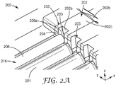
図2Aは、一部の実施形態による光フェルール200の斜視図であり、図2Bは、一部の実施形態による光フェルール200の平面図であり、図2Cは、一部の実施形態による光フェルール200の別の斜視図である。光フェルール200は、光導波路206を受け入れて固定するように構成された、少なくとも1つの受け入れ要素201を含む。図2A〜図2Cでは、光フェルール200の受け入れ要素201は、V字形状の溝として示されている。代替的には、この溝は、U字形状、Y字形状、又は任意の他の好適な形状を有し得る。
2A is a perspective view of the
光フェルール200は、少なくとも1つの光影響要素202を含む。図2A〜図2Cに示されるように、光影響要素202は、入力面202a、光方向転換素子202b、及び、それら入力面202aと光方向転換素子202bとの間の中間区画202cを備え得る。導波路206が、受け入れ要素201内に装着されると、その光導波路の出力面206aは、光影響要素202の入力面202aに光学的に結合される。光影響要素202は、光フェルール200内で伝播する、導波路206からの光の、1つ以上の特性に影響を及ぼす。
The
光ファイバ216は、コア、例えばガラスコアと、ガラスクラッドとを有する、導波路206を含み、それらのコア及びクラッドは、全内部反射によって、コア内部で光を伝播させるように構成されている。緩衝コーティング206bが、光ファイバ216の導波路206を包囲している。一部の実施形態では、この光ファイバはまた、ジャケット206cも含む。図2A〜図2Cに示されるように、光ファイバ216の導波路206のみが、受け入れ要素201内に挿入されるように、光ファイバ216の緩衝コーティング206b及びジャケット206cを剥ぎ取ることができる。スペース203は、光ファイバ216の導波路206にはアクセス不可能なものである。
The
一部の実施形態では、フェルール200は、導波路停止部204を含み、この導波路停止部204が、x軸に沿った導波路206の更なる移動を制限することにより、導波路206及び/又はフェルール200に損傷を与えることなく、溝201に沿って導波路206を更に押し込むことはできない。図2A〜図2Cに示されるように、導波路停止部204は、接着剤又は他の柔順性材料のための開口部205を有する、壁部を含み得る。導波路206の出力面206aと光影響要素202の入力面202aとの間の、スペース203は、導波路206にはアクセス不可能なものである。一部の実施形態では、導波路停止部204は、導波路206の更なる移動を停止させるように構成されていることにより、導波路206の出力面206aと光影響要素202の入力面202aとの間の、x軸に沿った距離210は、約10μm超、約40μm超、又は約80μm超、又は更に約160μm超となる。アクセス不可能スペース203は、光学接着剤、光学ゲル、又は光学油などの、柔順性の光学材料で充填することができる。例えば、フェルール200に導波路206を固定する、光学接着剤を使用することができる。例えば、この柔順性材料は、導波路206からの光が、導波路206の出力面206aと光影響要素202の入力面202aとの間のアクセス不可能スペース203を、実質的に妨げられずに通過して伝播することを可能にするように、選択することができる。
In some embodiments, the
図3Aは、一部の実施形態による光フェルール300の斜視図であり、図3Bは、一部の実施形態による光フェルール300の平面図であり、図3Cは、一部の実施形態による光フェルール300の別の斜視図である。光フェルール300は、光導波路306を受け入れて固定するように構成された、少なくとも1つの受け入れ要素301を含む。図3A〜図3Cでは、光フェルール300の受け入れ要素301は、センタリング側壁部301aを有する、Y字形状の溝として示されている。センタリング側壁部301aは、光影響要素302の入力面302aに対して、導波路306をy軸に沿って中心に配置するように、角度付けされている。
3A is a perspective view of the
光フェルール300は、少なくとも1つの光影響要素302を含む。図3A〜図3Cに示されるように、光影響要素302は、入力面302a、光方向転換素子302b、及び、それら入力面302aと光方向転換素子302bとの間の中間区画302cを備え得る。光影響要素302は、光フェルール300内で伝播する、導波路306からの光の、1つ以上の特性に影響を及ぼす。
The
フェルール300は、光影響要素の入力面302aに向けた、x軸に沿った導波路306の更なる動きを防ぐように構成されている、導波路停止部304を含む。導波路停止部304は、導波路306及び/又はフェルール300に損傷を与えることなく、導波路306が、光影響要素302の入力面302aに向けて、溝301内部で更に押し込まれることを防ぐ。図3A〜図3Cに示されるように、導波路停止部304は、導波路停止部304での溝301の側壁部間の距離が、導波路306の直径よりも小さくなる、センタリング特徴部301aに沿った位置を含み得る。導波路306の出力面306aと光影響要素302の入力面302aとの間の、スペース303(図3Bに示されるもの)は、導波路306にはアクセス不可能なものである。一部の実施形態では、導波路停止部304は、導波路306の更なる移動を停止させるように構成されていることにより、導波路306の出力面306aと光影響要素302の入力面302aとの間の、x軸に沿った距離310は、約10μm超、約40μm超、約80μm超、又は更に約160μm超となる。
The
アクセス不可能スペース303(図3Bを参照)は、光学接着剤、光学ゲル、又は光学油などの、柔順性の光学材料で充填することができる。例えば、フェルール300に導波路306を固定する、光学接着剤を使用することができる。この柔順性の光学材料は、導波路306からの光が、導波路306の出力面306aと光影響要素302の入力面302aとの間の、アクセス不可能スペース303(図3Bを参照)を、実質的に妨げられずに通過して伝播することを可能にするものである。
The inaccessible space 303 (see FIG. 3B) can be filled with a flexible optical material such as an optical adhesive, an optical gel, or an optical oil. For example, an optical adhesive that fixes the
光学装置又は光電子装置に対する、光導波路若しくは光ファイバの取り付けは、V字形状の溝(すなわち、V字溝)を使用して行われる場合が多い。導波路は、締め付け機構を使用して、その溝(典型的には、90°の角度のV字溝)の底部に押し込まれる。典型的には、次いで、屈折率整合接着剤を適用して、V字溝内に導波路を恒久的に保持する。この方策には、いくつかの課題がある。締め付け機構は、導波路を屈曲させて、それらの導波路を溝内に固定し、それにより、それらの導波路と溝とを位置合わせするために、十分な力を提供しなければならないが、導波路のリボンの各導波路に接触するためには、十分な柔順性も有さなければならない。締め付け機構はまた、それ自体が導波路に結合されることのない、接着剤を適用するためのアクセスも可能にしなければならない。V字溝の上に締め付け機構が位置することにより、導波路の位置を観察すること、又は、光硬化接着剤を使用することが困難となる。平坦な底部及び垂直な側壁部を備える、U字形状の溝(すなわち、U字溝)の使用には、いくつかの課題がある。導波路の捕捉の容易性に関する問題、及び、溝幅に必要とされる余裕空間に関連付けられた、位置誤差に関する問題は、これまでに対処されていない。 The attachment of the optical waveguide or optical fiber to the optical device or optoelectronic device is often performed using a V-shaped groove (that is, a V-shaped groove). The waveguide is pushed into the bottom of the groove (typically a V-groove at a 90 ° angle) using a tightening mechanism. Typically, a refractive index matching adhesive is then applied to permanently hold the waveguide in the V-groove. There are several challenges to this strategy. The tightening mechanism must provide sufficient force to bend the waveguides and secure them in the grooves, thereby aligning the waveguides with the grooves. There must also be sufficient flexibility to contact each waveguide on the waveguide ribbon. The tightening mechanism must also allow access for applying the adhesive, which itself is not coupled to the waveguide. The location of the tightening mechanism on the V-groove makes it difficult to observe the position of the waveguide or to use a photocurable adhesive. The use of U-shaped grooves (ie, U-grooves) with flat bottoms and vertical sidewalls presents several challenges. Problems related to the ease of capturing the waveguide and problems related to the positional error associated with the margin space required for the groove width have not been addressed so far.
実施形態は、1つ又は多数の光導波路を受け入れ、その光導波路に恒久的に取り付けられるように構成されている、1つ又は多数の溝を有する、光結合ユニットを目的とする。一実施形態では、溝の一部分には、光導波路を正しい位置へと横方向に屈曲させることを可能にする、略垂直な側壁部が設けられている。この溝は、上部をより広く形成することにより、その溝内に光導波路を捕捉することを容易にする、実質的にY字形状の断面(すなわち、Y字溝)をもたらすことができる。前述のように、光導波路は、単一モード光導波路、マルチモード光導波路、又は、単一モード若しくはマルチモード光導波路のアレイとすることができる。一部の実施形態では、導波路は、単一モード又はマルチモードのポリマー光導波路である。 An embodiment is intended for an optical coupling unit having one or more grooves that is configured to accept one or more optical waveguides and be permanently attached to the optical waveguide. In one embodiment, a portion of the groove is provided with a substantially vertical side wall that allows the optical waveguide to be laterally bent to the correct position. The groove can provide a substantially Y-shaped cross section (ie, a Y-groove) that facilitates capturing the optical waveguide within the groove by forming the top wider. As described above, the optical waveguide can be a single-mode optical waveguide, a multi-mode optical waveguide, or an array of single-mode or multi-mode optical waveguides. In some embodiments, the waveguide is a single-mode or multi-mode polymer optical waveguide.
別の実施形態では、溝の一部分には、光導波路を正しい位置へと横方向に屈曲させることを可能にする、略垂直な側壁部が設けられている。この溝の部分は、光導波路の直径よりも僅かに幅広に作製することにより、光導波路を最初に捕捉するための、余裕空間を提供することができる。溝の底部と接触して、その溝の底部に対して略平行になると、光導波路の端部は、溝の幅が徐々に狭くなり、その光導波路の直径よりも小さくなる場所へと、軸方向に摺動される。この場所で、光導波路の先端が停止して、正しく位置決めされる。この溝は、一部の実施形態によれば、上部をより広く形成することにより、その溝内に光導波路を捕捉することを容易にする、実質的にY字形状の断面をもたらすことができる。 In another embodiment, a portion of the groove is provided with a substantially vertical side wall that allows the optical waveguide to be laterally bent to the correct position. By making the groove portion slightly wider than the diameter of the optical waveguide, it is possible to provide a margin space for initially capturing the optical waveguide. When in contact with the bottom of the groove and approximately parallel to the bottom of the groove, the end of the optical waveguide shafts to a location where the width of the groove gradually narrows and becomes smaller than the diameter of the optical waveguide. Sliding in the direction. At this point, the tip of the optical waveguide stops and is properly positioned. This groove, according to some embodiments, can provide a substantially Y-shaped cross section that facilitates capturing the optical waveguide within the groove by forming the top wider. ..
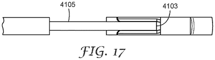
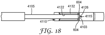
図4は、様々な実施形態による、LCU4100の一部分を示す。図4に示されるLCU4100は、単一のLCU取り付け区域4102を含む。図4では、単一のLCU取り付け区域4102が示されているが、多数の光導波路を受け入れ、それら光導波路に恒久的に取り付けるために、多数の取り付け区域4102を、LCU4100上に設けることができる点が理解されよう。LCU取り付け区域4102は、入口4111、終端部4113、及び、それら入口4111と終端部4113との間に延びる中心面4112(図5を参照)を有する、Y字溝4110を含む。中心面4112は、図5に示されるように、Y字溝4110の底面4125を二等分し、かつ底面4125から垂直に延びる、平面である。Y字溝4110は、図5に示される略円筒形の導波路4105などの、光導波路を受け入れるように構成されている。
FIG. 4 shows a portion of the LCU4100 according to various embodiments. The
LCU4100は、光方向転換部材4104、及び、その光方向転換部材4104と終端部4113との間の中間区画4108を含む。一部の実施形態では、終端部4113は、レンズなどの光学的透明部材を備えるものであり、又は、光透過性材料から形成されている。中間区画4108は、光透過性材料から形成されている。光方向転換部材4104は、出力側4106を含み、光は、この出力側4106を通って、その光方向転換部材4104から出射される(又は、光方向転換部材4104内に入射する)。
The
一部の実施形態によれば、図4及び図5を参照すると、Y字溝4110は、略U字形状の下側部分4120と、拡張された上側部分とによって形成された複合溝であり、この拡張された上側部分が、この複合溝を略Y字形状にしている。溝という用語を修飾している、U字及びY字という用語は、便宜上、これらの溝の近似的形状を暗示するために役立つものであり、限定するものではないことが理解されよう。
According to some embodiments, with reference to FIGS. 4 and 5, the Y-
図5で最も良好に示されるように、Y字溝4110は、第1領域4120’、第2領域4130’、開口部4140、及び底面4125によって画定されている。第1領域4120’は、底面4125と第2領域4130’との間に画定されている。第1領域4120’は、間隔Sによって隔てられた、実質的に平行な側壁部4122を含む。これら側壁部4122は、垂直から外れた方向で、1度又は数度(例えば、<約10度)の抜き勾配を有し得るものであり、それゆえ、互いに対して実質的に平行であると見なすことができる。例えば、側壁部4122は、底面4125に対して垂直〜約5度以内とすることができる。側壁部4122は、製造の間の側壁部4122の離型を容易にするために、僅かに外向きの傾斜又は抜き勾配を有し得る。この場合、それらの実質的に垂直な側壁部4122は、底面4125から垂直に延びる平面4112と、抜き勾配角度αを成している。
As best shown in FIG. 5, the Y-
第2領域4130’は、第1領域4120’と開口部4140との間に配設されている。開口部4140は、Y字溝4110の頂部表面4127間に画定されている。開口部4140の幅Wは、側壁部4122間の間隔Sよりも大きい。図42で見ることができるように、第1領域4120’は、Y字溝4110のU字形状の下側部分4120を画定し、第2領域4130’は、拡張された上側部分4130を画定している。
The second region 4130'is arranged between the first region 4120' and the
第2領域4130’は、Y字溝4110の中心面4112から外向きに延びる、側壁部4132を含む。図42では、側壁部4132は、面取り側壁部と見なすことが可能な、直線状の側壁部を備える。他の実施形態では、側壁部4132は、ある程度の湾曲を有することなどによって、非直線状とすることができる。側壁部4132は、第1領域4120’と開口部4140との間に延びており、それら側壁部4132間の間隔は、第1領域4120’から開口部4140まで、漸進的に増大している。
The second region 4130'includes a
一部の実施形態によれば、開口部4140の幅Wは、第1領域4120’の間隔Sよりも、その間隔Sの約半分に等しい距離分で大きい。他の実施形態では、開口部4140の幅Wは、間隔Sよりも、その間隔Sの約半分よりも大きい距離分で大きい。第1領域4120’の側壁部4122の高さは、導波路4105の高さの約50%よりも大きいものとすることができる。例えば、第1領域4120’の側壁部4120の高さは、光導波路4105の高さの約50%〜75%の範囲とすることができる。一部の実施形態では、第1領域4120’の側壁部4122の高さは、約62.5〜65μmよりも大きいが、光導波路4105の高さよりも小さくすることができる。他の実施形態では、第1領域4120’の側壁部4122の高さは、約75μmよりも大きいが、光導波路4105の高さよりも小さくすることができる。図5に示される実施形態では、Y字溝4110の全高は、導波路4105の高さ(例えば、約125μm)に略等しい。一部の実施形態では、Y字溝4110の全高は、導波路4105の高さより小さくすることも、又は大きくすることもできる。カバー4135(任意選択)は、光導波路4105、及びLCU4100の溝4110を覆うように構成することができる。
According to some embodiments, the width W of the
図5で見ることができるように、光導波路4105に最接近した領域での、第1領域4120’の側壁部4122間の間隔は、所定の余裕空間の分、導波路の幅よりも大きい。一部の実施形態では、この所定の余裕空間は、約1μm未満とすることができる。他の実施形態では、この所定の余裕空間は、約1〜3μmとすることができる。更なる実施形態では、この所定の余裕空間は、約1〜5μmとすることができる。例えば、光導波路4105は、約125μmの幅を有し得るものであり、第1領域4120’の側壁部4122を隔てる間隔は、約1〜5μmの余裕空間を含み得る。
As can be seen in FIG. 5, the distance between the
マルチモードファイバを備える導波路4105を採用する実施形態では、この所定の余裕空間は、約1〜5μmとすることができる。例えば、この所定の余裕空間は、マルチモードファイバを備える光導波路4105の幅の、約0.8〜4%に等しいものとすることができる。単一モードファイバを備える導波路4105を採用する実施形態では、この所定の余裕空間は、約0〜2μmとすることができる。例えば、この所定の余裕空間は、単一モードファイバを備える光導波路4105の幅の、約0〜1.6%に等しいものとすることができる。一部の場合には、この余裕空間を0未満にすることができ、それにより、導波路4105は、Y字溝4110内に配置された場合に、そのY字溝4110を変形させる。
In the embodiment in which the
図5及び図6に示される導波路4105は、クラッド4109によって包囲されたコア4107を含む。コア4107は、導波路4105が、光学的(屈折率整合)結合材料を使用して、Y字溝4110内部の適所に恒久的に結合される場合に、光方向転換部材(図41の4104を参照)と光学的に位置合わせされることが重要である。一部の実施形態では、Y字溝4110は、センタリング構成を含み、このセンタリング構成によって、導波路4105は、その導波路4105がY字溝4110内に装着された際に、Y字溝4110の中心面4112に向けて、横方向に強制的に誘導される。Y字溝4110の中心面4112に沿って、コア4107を中心に配置することに加えて、このセンタリング構成は、Y字溝4110内部での導波路4105の軸方向変位を制限する、導波路停止部を提供する。それゆえ、一部の実施形態による複合Y字溝4110は、U字溝のみと組み合わせた、又はY字溝と組み合わせた、センタリング構成を含む。
The
図4及び図6は、第1の端部4115’及び第2の端部4115’’を備える長手方向移行区画4115によって画定された、センタリング構成が組み込まれている、Y字溝4110を示す。第1の端部4115’は、第1領域4120’の側壁部4122間の間隔Sに等しい幅を有する。第2の端部4115’’は、光導波路4105の幅よりも小さい幅を有する。側壁部の間隔は、それらの側壁部が、移行区画4115内で内向きに角度付けされていることなどによって、その移行区画4115内部で漸進的に低減している。移行区画4115は、側壁部4122の終端部から開始して、Y字溝4110の中心面に向けて内向きに突出することが可能な、センタリング側壁部4126を備える。センタリング側壁部4126は、Y字溝4110の面取り側壁部と見なすこともできる。側壁部4122、及び移行区画4115のセンタリング側壁部4126は、実質的に平坦な側壁表面、又は非平坦な側壁表面を備え得る。
4 and 6 show a Y-
センタリング側壁部4126は、側壁部4122に対して、約5〜45度の範囲とすることが可能な、角度βを成している。この長手方向移行区画4115は、Y字溝4110の全長に対して、それほど長いものである必要はない。例えば、Y字溝4110の長さは、200μm〜2000μmとすることができ、センタリング側壁部4126は、側壁部4122から、約2μm〜50μmの距離で延びることができる。センタリング側壁部4126は、側壁部4122と同じ高さを有し得る。
The centering
導波路4105が、Y字溝4110内部で、光方向転換部材4104に向けて軸方向に変位されると、導波路4105の終端部4103が、センタリング側壁部4126に接触して、Y字溝4110の中心面に向けて誘導されることにより、導波路4105の中心軸が、Y字溝4110内部で中心に配置される。それらセンタリング側壁部4126の終端部間には、間隙4129が画定されている。この間隙4129は、導波路4105のコア4107から放射される光が、妨げられずに通過することを可能にするほど、十分に広いものである。センタリング側壁部4126の長さ、及び間隙4129の幅は、好ましくは、導波路4105のコア及びクラッドの寸法に適応するようにサイズ設定される。導波路4105の終端部4103が、このセンタリング構成によって、Y字溝4110内部で適切に中心に配置されている場合、クラッド4109は、導波路停止部604の位置で、センタリング側壁部4126と接触しており、コア4107は、間隙4129の中心と位置合わせされている。図43に示されるセンタリング構成は、U字溝内で、又は、Y字溝などの複合U字溝内で実装することができる点が理解されよう。
When the
図7は、様々な実施形態による、LCU4100のLCU取り付け区域4102の上面図を示す。図7に示されるLCU取り付け区域4102は、Y字溝4110内部で中心に配置されている、導波路4105の終端部4103を示す。図7に示されるY字溝4110の実施形態は、Y字溝4110の入口4111と長手方向移行区画4115との間に、位置合わせ特徴部を含む。この位置合わせ特徴部は、溝側壁部4122の突出区画4124を含む。対向する突出区画4124間の間隔は、導波路4105の幅よりも僅かに大きく、対向する側壁部4122間の間隔よりも僅かに小さい。この位置合わせ特徴部の突出区画4124は、導波路の端部4103が、Y字溝4110の移行区画4115内に位置決めされる際に、そのY字溝4110の中心面に対する導波路4105の角度合わせを提供するために役立つ。一部の実施形態では、突出区画4124によって形成されている、この位置合わせ特徴部は、溝入口4111に、又は溝入口4111付近に配置されている。
FIG. 7 shows a top view of the
図7に示される実施形態では、導波路4105の終端部4103の縁部は、導波路停止部604の位置で、移行区画4115のセンタリング壁部4126内に、僅かに埋め込まれて示されている。この実施形態では、導波路4105のクラッド4109は、センタリング壁部4126を形成するために使用された材料よりも硬い材料(例えば、ガラス)で形成されている。センタリング壁部4126内の変形4128は、導波路4105の終端部4103が、その中心に配置された位置で、センタリング壁部4126に当接する際に、その導波路4105に、軸方向に向けた力を加えることによって、形成することができる。この変形4128は、Y字溝4110内部に導波路4105を恒久的に結合するために、光学的結合材料が適用される場合に、Y字溝4110内部で、適切に中心に配置された導波路4105の位置決めを維持するために役立つ。
In the embodiment shown in FIG. 7, the edge of the
図7に示されるY字溝4110の実施形態には、Y字溝4110の側壁部4122と導波路4105の外周との間に画定された、結合領域4123が組み込まれている。結合領域4123は、結合材料(例えば、光学的結合材料)で充填することができ、この結合材料は、硬化すると、Y字溝4110内部に導波路4105を恒久的に結合する。一部の実施形態では、結合領域4123は、導波路4105と、平坦底面4125と、側壁部4122との間の容積として画定される。他の実施形態では、Y字溝4110内部に捕捉される結合材料の体積を増大させるために、底面4125が側壁部4122に接している、側壁部4122の一部分に沿って、凹付き部又は細長い窪みを形成することができる。
The embodiment of the Y-
図7はまた、硬化した場合に、導波路4105の終端部4103とLCU取り付け区域4102との結合の強度(例えば、完全性)を向上させるために役立つ、ある体積の光学的結合材料を受け入れるように構成された、前方接着剤空洞部4131も示す。一部の実施形態では、接着剤空洞部4131は、導波路4105の端部からの光を伝送するように構成されている。図8に示されているように、前方接着剤空洞部4131は、LCU取り付け区域4102の底面4125内に形成された、凹付き部4131’を含み得る。凹付き部4131’は、光学的結合材料を受け入れるための、前方接着剤空洞部4131の総容積を増大させるために役立ち、それにより、導波路4105の終端部4103とLCU取り付け区域4102との結合の強度/完全性が向上する。図9はまた、溝110の底面4125が傾斜から水平状態に移行する場所4133の、Y字溝4110の入口4111も示す。
FIG. 7 also accepts a volume of optical coupling material that, when cured, helps to improve the strength (eg, integrity) of the coupling between the
図9は、図7に示された結合領域4123及び前方接着剤空洞部4131を示し、更には、Y字溝4110の各側壁部4122から横方向に延びる、側方接着剤空洞部4121を示す。側方接着剤空洞部4121は、結合領域4123の延長部分とすることができる。側方接着剤空洞部4121は、導波路4105の終端部103の側部付近に、追加的な結合材料を受け入れるための容積を提供するものであり、これにより、Y字溝4110と導波路4105との結合の強度/完全性が向上する。図10に示されているように、側方接着剤空洞部4121は、LCU取り付け区域4102の底面4125内に形成された、凹付き部4121’を含み得る。凹付き部4121’は、光学的結合材料を受け入れるための、側方接着剤空洞部4121の総容積を増大させるために役立ち、それにより、導波路4105とY字溝4110との結合の強度/完全性が向上する。
FIG. 9 shows the
図11は、多数の溝4110を備える、LCU取り付け区域4102を示すものであり、各溝4110には、内部に導波路4105が配設されている。図11では、2つの溝4110が示され、それぞれの導波路4105は、導波路停止部604の位置での、溝4110内部の中心に配置された位置で、センタリング表面4126と接触している。図11は、前方接着剤空洞部4131に隣接して配置された、接着剤リザーバ4131’’を示す。接着剤リザーバ4131’’は、2つ以上の前方接着剤空洞部4131間で共有されている、LCU取り付け区域4102の容積である。この点に関して、接着剤リザーバ4131’’は、2つ以上の前方接着剤空洞部4131に流体結合されている。接着剤リザーバ4131’’は、導波路4105の終端部4103付近に、追加的な結合材料を受け入れるための容積を提供するものであり、これにより、導波路4105とLCU取り付け区域4102との結合の強度/完全性が向上する。
FIG. 11 shows an
図12〜図17は、様々な実施形態による、LCU取り付け区域4102のY字溝4110内に、導波路4105を装着するためのプロセスを示す。一部の実施形態では、この装着プロセスは、図12及び図13に示されるものと同様の図(例えば、上面図、側面図)を提供するために、デジタルカメラと共に顕微鏡を使用して監視することができる。Y字溝4110内部に位置決めされる導波路4105が示されており、この導波路4105は、その導波路4105を包囲する緩衝材4116から延びている。緩衝材4106は、典型的には、導波路4105を保護するために役立つ、ポリマーシースである。
12 to 17 show the process for mounting the
最初に、導波路4105を、終端部4103が小さい角度(例えば、5°〜20°)で下方を向く状態で、Y字溝4110の拡張領域(すなわち、上部領域)の上に位置決めする。図12及び図13は、導波路4105が、最初にY字溝4110内部で位置ずれしている、典型的実施例を示す。Y字溝4110の上部拡張領域は、導波路4105を捕捉して、Y字溝4110のU字溝領域(すなわち、下部領域)内に導波路4105を導くために役立つ、角度付けされた側面4132を含む。導波路4105の終端部4103を降下させると、その終端部4103は、Y字溝領域の一方の側の捕捉側壁部4132に接触し、この捕捉側壁部4132が、導波路4105を、強制的に横方向に屈曲及び/又は移動させて、Y字溝4110の底部領域(すなわち、U字溝領域)内に、終端部4103を誘導する。
First, the
導波路4105をY字溝4110内に降下させると(図14を参照)、終端部4103は、Y字溝4110の底面4125によって、上向きに屈曲される。同時に、Y字溝4110が、引き続き導波路4105を横方向に屈曲及び/又は移動させることにより、導波路4105は、Y字溝4110のU字溝領域の、略垂直な壁部4122によって拘束される(図15を参照)。導波路4105が、図16に示されているように、略水平になる(すなわち、Y字溝4110の底面4125に接する)と、終端部4103がセンタリング表面4126に接触するまで(図18を参照)、導波路4105を、Y字溝4110の長手方向移行区画4115内へと、前方に押し込む(図17を参照)。センタリング表面4126は、終端部4103が、導波路停止部604の位置で、Y字溝4110の両側のセンタリング表面4126と接触するまで、導波路4105の終端部4103を、必要に応じて横方向に押すことにより、図18で最も良好に示されるように、導波路4105の終端部4103を、Y字溝4110内の中心に正確に配置する。
When the
センタリング表面4126によって中心に配置された場合の、導波路4105の最終的な角度は、典型的には水平であり、その角度は、任意の好適な機械的手段によって制御することができ、図16に示される図などの側面図の光学検査によって、任意選択的に誘導することができる。図19は、導波路4105が過度に降下されることにより、Y字溝4110の底面4125の後縁部4125’と接触する場合に生じる恐れがある、位置合わせ誤差を示す。このシナリオでは、導波路4105の終端部4103は、てこの作用により、Y字溝4110から外に持ち上げられている。この位置ずれは、Y字溝4110の終端部4113の比較的短いポーチ領域4125’’(図20)のみを残して、Y字溝4110の底面4125の殆どを凹付きにさせることによって、大いに低減される。
The final angle of the
図20で見ることができるように、底面4125’’’の大部分は、Y字溝4110の終端部4113に隣接するポーチ領域4125’’に対して、凹付きにしている。一部の実施形態では、このY字溝4110の底面4125の凹付きの区画4125’’’は、Y字溝4110の入口4111から終端部4113に向けて延び、底面4125の表面積の約2分の1を超えて広がることができる。例えば、凹付きの区画4125’’’は、Y字溝4110の入口4111から延びて、終端部4113から、ある距離の範囲内に至ることができ、この距離は、Y字溝4110によって受け入れられる導波路4105高さの約2倍未満である。典型的には、凹付きの区画4125’’’の少なくとも一部分は、導波路4105が十分に支持されるように、硬化した光学接着剤で充填される。
As can be seen in FIG. 20, most of the
下部U字溝及び拡張上部溝を備える、複合Y字溝4110は、熱可塑性樹脂(例えば、Ultem)の射出成形で製造することができる。そのような材料は、ガラス光ファイバよりも遥かに大きい熱膨張係数を有する。それゆえ、コンピュータシャーシ内での動作時に生じ得るような、熱逸脱によって引き起こされる応力が懸念される。これらの応力は、Y字溝4110を含む部分の反りによる、光学的位置ずれをもたらす恐れがあり、又は更に、導波路4105を結合するために使用される、接着剤の損傷をもたらす恐れもある。そのような応力を最小限に抑えるために、接着剤で充填されるY字溝4110の長さを最小化することが望ましい。しかしながら、導波路4105の角度を拘束するためには、十分な溝の長さが必要とされる。必要とされるY字溝4110の長さは、その光学システムの角度公差に応じて、及び、導波路4105に余裕空間を提供するために含められる、そのY字溝4110の追加的な幅に応じて決定される。
The composite Y-
図21〜図23は、2つの別個の区画4110a及び区画4110bを有する、Y字溝4110を示す。導波路4105の終端部4103付近で、短い区画が、長手方向移行区画4115及びセンタリング表面4126を含む。導波路の更なる軸方向移動は、導波路停止部604によって制限される。この区画4110aは、屈折率整合接着剤で充填することができる。別個の区画4110bが、導波路4105の正確な角度合わせを実現するように、区画4110bから、ある程度の十分な距離(例えば、0.5mm)で配置されているが、この区画4110bは、接着剤で充填されていない。この設計により、角度合わせに支障を来すことなく、熱膨張に関連付けられる応力が、(結合長を最小限に抑えることによって)最小限に抑えられる。
21 to 23 show a Y-
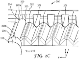
図24は、様々な実施形態による、LCU6100の一部分を示す。図24に示されるLCU6100は、単一のLCU取り付け区域6102を含む。図24では、単一のLCU取り付け区域6102が示されているが、多数の光導波路を受け入れ、それら光導波路に恒久的に取り付けるために、多数の取り付け区域6102を、LCU6100上に設けることができる点が理解されよう。LCU取り付け区域6102は、入口6111及び終端部6113を有する、溝6110を含む。溝6110は、図5に示される略円筒形の導波路4105などの、光導波路を受け入れるように構成されている。
FIG. 24 shows a portion of the
LCU6100は、光方向転換部材(図24には示されないが、図4の4104を参照)及び、その光方向転換部材と終端部6113との間の中間区画6108を含む。一部の実施形態では、終端部6113は、レンズなどの光学的透明部材を備えるものであり、又は、光透過性材料から形成されている。中間区画6108は、光透過性材料から形成されている。光方向転換部材は、出力側を含み、光は、この出力側を通って、その光方向転換部材から出射される(又は、光方向転換部材内に入射する)。
The
一部の実施形態によれば、上記で詳細に説明されているように、溝6110は、略U字形状の下側部分6123と、拡張された上側部分6127、6132とによって形成された複合溝であり、この拡張された上側部分が、この複合溝を略Y字形状(Y字溝)にしている。溝6110は、単一のセンタリング側壁部6126を含む、長手方向移行区画6115を含む。長手方向移行区画6115内部では、側壁部6122と側壁部6122’との間隔は、光導波路6105の幅に余裕空間を加えたものと等しい幅から、光導波路6105の幅よりも小さい幅へと低減している。図24に示される実施形態では、側壁部6122の一方は、溝6110の入口6111と終端部6113との間で、実質的に平坦である。対向する側壁部6122’は、側壁部6122に実質的に平行な側壁部分を含み、移行区画6115内で、内向きに角度付けされたセンタリング側壁部6126へと移行する。センタリング側壁部6126は、溝6110の面取り側壁部と見なすこともできる。
According to some embodiments, as described in detail above, the
図24では、溝6110は、溝6110の一方の側のみに、センタリング側壁部6126を含む。それゆえ、この単一のセンタリング側壁部6126を、位置決め側壁部6126と見なすことができる。組み立ての間に、光導波路6105は、図24に示されているように、位置決め側壁部6126が、光導波路6105を、溝6110内部の導波路停止部604の位置で押し留めるまで、平坦な側壁部6122に沿って摺動される。この場所で、位置決め側壁部6126は、導波路停止部604としての機能を果たし、溝6110内部での、光導波路6105の終端部6103の、更なる長手方向の前進を防ぐ。図24に示される実施形態の1つの利点は、組み立ての間に、光導波路6105の角度を良好に制御することができる点であるが、これは、光導波路6105が、側壁部6122に平行に屈曲することができるためである。一部の実施形態では、位置決め側壁部6126は、光導波路6105が、組み立ての間に側壁部6122に対して屈曲することができる限り、光導波路6105を挟み込む必要はなく、その代わりに、溝6110の端部、又は何らかの他の障壁を画定することなどによって、従来の停止部としての機能を果たすことができる。
In FIG. 24, the
本明細書で説明される手法と併せて使用することが可能な、フェルール、位置合わせフレーム、及びコネクタに関する更なる情報が、参照により本明細書に組み込まれる、同一出願人による同時出願の、以下の米国特許出願で提示されている:表題「Connector with Latching Mechanism」を有し、代理人整理番号76663US002によって識別される、米国特許出願第62/239,998号;表題「Optical Ferrules」を有し、代理人整理番号76982US002によって識別される、米国特許出願第62/240,069号;表題「Ferrules,Alignment Frames and Connectors」を有し、代理人整理番号75767US002によって識別される、米国特許出願第62/240,066号;表題「Optical Coupling Device with Waveguide Assisted Registration」を有し、代理人整理番号76660US002によって識別される、米国特許出願第62/240,010号;表題「Optical Cable Assembly with Retainer」を有し、代理人整理番号76662US002によって識別される、米国特許出願第62/240,008号;表題「Dust Mitigating Optical Connector」を有し、代理人整理番号76664US002によって識別される、米国特許出願第62/240,000号;表題「Optical Waveguide Registration Feature」を有し、代理人整理番号76661US002によって識別される、米国特許出願第62/240,009号;表題「Optical Ferrules and Optical Ferrule Molds」を有し、代理人整理番号75985US002によって識別される、米国特許出願第62/239,996号;表題「Configurable Modular Connectors」を有し、代理人整理番号76907US002によって識別される、米国特許出願第62/240,003号;及び、表題「Hybrid Connectors」を有し、代理人整理番号76908US002によって識別される、米国特許出願第62/240,005号。 Further information about ferrules, alignment frames, and connectors that can be used in conjunction with the techniques described herein is incorporated herein by reference in a simultaneous application by the same applicant, below. Presented in the US Patent Application of: US Patent Application No. 62 / 239,998, having the title "Connector with Latching Mechanism" and identified by agent reference number 76663US002; having the title "Optical Ferrules". US Pat. / 240,066; US Patent Application No. 62 / 240,010; title "Optical Cable US Pat. / 240,000; US Patent Application No. 62 / 240,009, having the title "Optical Waveguide Regency Feture" and identified by agent reference number 76661US002; having the title "Optical Ferrules and Optical Festival". US Pat. No. 003; and has the title "Hybrid Patentors" and has an agent reference number 76908US002. U.S. Patent Application No. 62 / 240,005, identified by.
本開示で説明される項目には、以下のものが含まれる:
項目1.光フェルールであって、
光導波路からの光が光フェルール内で伝播する際に、その光の1つ以上の特性に影響を及ぼすように構成されている、少なくとも1つの光影響要素であって、この光影響要素が、入力面を有する、少なくとも1つの光影響要素と、
光導波路を受け入れて固定することにより、光影響要素の入力面に、その導波路の出力面が光学的に結合されるように構成されている、少なくとも1つの受け入れ要素と、
受け入れ要素内に光導波路が装着された際に、光影響要素の入力面に向けた、その導波路の移動を制限するように構成されている、導波路停止部と、
受け入れ要素内に光導波路が装着された際に、その光導波路にはアクセス不可能な、光導波路の出力面と光影響要素の入力面との間のスペースとを備える、光フェルール。
The items described in this disclosure include:
Item 1. It ’s an optical ferrule,
At least one light-influencing element that is configured to affect one or more properties of the light as it propagates within the optical waveguide. With at least one optical waveguide having an input surface,
With at least one receiving element configured to optically couple the output surface of the waveguide to the input surface of the optical waveguide by accepting and fixing the optical waveguide.
A waveguide stop that is configured to limit the movement of the waveguide towards the input surface of the light-affecting element when the optical waveguide is mounted within the receiving element.
An optical ferrule that provides a space between the output surface of an optical waveguide and the input surface of a light-affecting element that is inaccessible to the optical waveguide when it is mounted within the receiving element.
項目2.受け入れ要素が、1つ以上の溝を含む、項目1の光フェルール。 Item 2. Item 1 optical ferrule, wherein the receiving element contains one or more grooves.
項目3.受け入れ要素が、1つ以上の穴を含む、項目1の光フェルール。 Item 3. Item 1 optical ferrule, wherein the receiving element contains one or more holes.
項目4.受け入れ要素が、少なくとも1つの円筒形の穴を含む、項目1の光フェルール。 Item 4. The optical ferrule of item 1, wherein the receiving element comprises at least one cylindrical hole.
項目5.光フェルールが、単芯光ファイバフェルールである、項目1〜項目4のうちのいずれかの光フェルール。 Item 5. The optical ferrule according to any one of items 1 to 4, wherein the optical ferrule is a single-core optical fiber ferrule.
項目6.光フェルールが、多芯光ファイバフェルールである、項目1〜項目4のうちのいずれかの光フェルール。 Item 6. The optical ferrule according to any one of items 1 to 4, wherein the optical ferrule is a multi-core optical fiber ferrule.
項目7.受け入れ要素が、U字形状の溝である、項目1の光フェルール。 Item 7. Item 1 optical ferrule in which the receiving element is a U-shaped groove.
項目8.導波路停止部が、導波路の直径よりもU字形状の溝の幅が小さい位置を含む、項目7の光フェルール。 Item 8. Item 7. The optical ferrule of item 7, wherein the waveguide stop includes a position where the width of the U-shaped groove is smaller than the diameter of the waveguide.
項目9.U字形状の溝が、そのU字形状の溝内部で光導波路を中心に配置するように構成された、センタリング側壁部を含む、項目7の光フェルール。 Item 9. Item 7. The optical ferrule of item 7, wherein the U-shaped groove is configured to center the optical waveguide inside the U-shaped groove, including a centering side wall.
項目10.U字形状の溝が、そのU字形状の溝内部で光導波路を位置決めするように構成された、少なくとも1つのセンタリング側壁部を含む、項目7の光フェルール。 Item 10. Item 7. The optical ferrule of item 7, wherein the U-shaped groove comprises at least one centering side wall portion configured to position the optical waveguide within the U-shaped groove.
項目11.受け入れ要素が、V字形状の溝である、項目1の光フェルール。
項目12.受け入れ要素が、Y字形状の溝である、項目1の光フェルール。 Item 12. Item 1 optical ferrule in which the receiving element is a Y-shaped groove.
項目13.導波路停止部が、導波路の直径よりもY字形状の溝の幅が小さい位置を含む、項目12の光フェルール。 Item 13. Item 12. The optical ferrule of item 12, wherein the waveguide stop includes a position where the width of the Y-shaped groove is smaller than the diameter of the waveguide.
項目14.Y字形状の溝が、そのY字形状の溝内部で光導波路を位置決めするように構成された、1つ以上のセンタリング側壁部を含む、項目12の光フェルール。 Item 14. Item 12. The optical ferrule of item 12, wherein the Y-shaped groove comprises one or more centering sidewalls configured to position the optical waveguide within the Y-shaped groove.
項目15.Y字形状の溝が、そのY字形状の溝内部で光導波路を位置決めするように構成された、少なくとも1つのセンタリング側壁部を含む、項目12の光フェルール。 Item 15. Item 12. The optical ferrule of item 12, wherein the Y-shaped groove comprises at least one centering side wall portion configured to position the optical waveguide within the Y-shaped groove.
項目16.センタリング側壁部間の幅が、溝の長手方向軸に沿って、入力面に向けた方向で漸進的に狭くなる、項目12の光フェルール。 Item 16. Item 12. The optical ferrule of item 12, wherein the width between the centering sidewalls gradually narrows in the direction toward the input surface along the longitudinal axis of the groove.
項目17.導波路停止部が、導波路の直径よりもセンタリング側壁部間の幅が小さい位置を含む、項目16の光フェルール。 Item 17. The optical ferrule of item 16, wherein the waveguide stop includes a position where the width between the centering sidewalls is smaller than the diameter of the waveguide.
項目18.導波路停止部が壁部を含む、項目1〜項目17のうちのいずれかの光フェルール。 Item 18. The optical ferrule according to any one of items 1 to 17, wherein the waveguide stop portion includes a wall portion.
項目19.光影響要素がレンズを含む、項目1〜項目18のうちのいずれかの光フェルール。 Item 19. A light ferrule according to any one of items 1 to 18, wherein the light influencing element includes a lens.
項目20.光影響要素が、光導波路からの光を方向転換させるように構成された要素を含む、項目1〜項目19のうちのいずれかの光フェルール。 Item 20. The optical ferrule according to any one of items 1 to 19, wherein the light influencing element comprises an element configured to divert light from an optical waveguide.
項目21.導波路アクセス不可能スペースが、導波路の出力面と光影響要素の入力面との間で、光が妨げられずに伝播することを可能にするように構成されている、項目1〜項目20のうちのいずれかの光フェルール。 Item 21. Items 1 to 20 the waveguide inaccessible space is configured to allow light to propagate unimpeded between the output surface of the waveguide and the input surface of the light-affecting element. One of the optical ferrules.
項目22.導波路アクセス不可能スペースが、接着剤リザーバを含む、項目1〜項目21のうちのいずれかの光フェルール。 Item 22. The optical ferrule of any of items 1 to 21, wherein the waveguide inaccessible space includes an adhesive reservoir.
項目23.導波路アクセス不可能スペースが、柔順性材料を収容するように構成されている、項目1〜項目22のうちのいずれかの光フェルール。 Item 23. The optical ferrule of any of items 1-22, wherein the waveguide inaccessible space is configured to accommodate the flexible material.
項目24.柔順性材料が、光学接着剤、光学ゲル、及び光学油のうちの1つ以上である、項目23の光フェルール。 Item 24. The optical ferrule of item 23, wherein the flexible material is one or more of an optical adhesive, an optical gel, and an optical oil.
項目25.導波路の出力面と光影響要素の入力面との間の距離が、約10μmよりも大きい、項目1〜項目24のうちのいずれかの光フェルール。 Item 25. The optical ferrule according to any one of items 1 to 24, wherein the distance between the output surface of the waveguide and the input surface of the optical influence element is larger than about 10 μm.
項目26.導波路の出力面と光影響要素の入力面との間の距離が、約40μmよりも大きい、項目1〜項目24のうちのいずれかの光フェルール。 Item 26. The optical ferrule according to any one of items 1 to 24, wherein the distance between the output surface of the waveguide and the input surface of the optical influence element is larger than about 40 μm.
項目27.導波路停止部と光影響要素の入力面との間の距離が、約10μmよりも大きくなるように、導波路停止部が位置決めされている、項目1〜項目24のうちのいずれかの光フェルール。 Item 27. The optical ferrule of any of items 1 to 24, wherein the waveguide stop is positioned so that the distance between the waveguide stop and the input surface of the optical influence element is greater than about 10 μm. ..
項目28.導波路停止部と光影響要素の入力面との間の距離が、約40μmよりも大きくなるように、導波路停止部が位置決めされている、項目1〜項目24のうちのいずれかの光フェルール。 Item 28. The optical ferrule of any of items 1 to 24, wherein the waveguide stop is positioned so that the distance between the waveguide stop and the input surface of the optical influence element is greater than about 40 μm. ..
項目29.光導波路が、接着剤によって受け入れ要素に固定されている、項目1〜項目28のうちのいずれかの光フェルール。 Item 29. The optical ferrule according to any one of items 1 to 28, wherein the optical waveguide is fixed to the receiving element by an adhesive.
項目30.接着剤が、光導波路からの光に対して実質的に透過性である、項目29の光フェルール。 Item 30. 29. The optical ferrule of item 29, wherein the adhesive is substantially transparent to light from the optical waveguide.
項目31.接着剤が、アクセス不可能スペース内にもまた配設されている、項目29の光フェルール。 Item 31. The optical ferrule of item 29, wherein the adhesive is also disposed in the inaccessible space.
項目32.光透過性材料が、アクセス不可能スペース内に配設されている、項目29の光フェルール。 Item 32. The optical ferrule of item 29, wherein the light transmissive material is disposed in an inaccessible space.
項目33.光透過性材料が、接着剤とは異なる、項目32の光フェルール。 Item 33. The light ferrule of item 32, wherein the light transmissive material is different from the adhesive.
項目34.接着剤が、光導波路からの光に対して透過性ではない、項目29の光フェルール。 Item 34. The optical ferrule of item 29, wherein the adhesive is not transparent to light from the optical waveguide.
項目35.光フェルールであって、
光導波路を受け入れて固定するように構成されている、少なくとも1つの溝と、
光導波路からの光が光フェルール内で伝播する際に、その光の1つ以上の特性に影響を及ぼすように構成されている、少なくとも1つの光影響要素であって、この光影響要素が、溝の近位に入力面を有する、少なくとも1つの光影響要素と、
光影響要素の入力面の近位で溝内に配設されている、導波路停止部であって、その入力面に向けた光導波路の動きを制限するように構成されている、導波路停止部と、
溝内に光導波路が装着された際に、その光導波路にはアクセス不可能な、光影響要素の入力面と光導波路の出力面との間のスペースとを備える、光フェルール。
Item 35. It ’s an optical ferrule,
With at least one groove configured to accept and secure the optical waveguide,
At least one light-influencing element that is configured to affect one or more properties of the light as it propagates within the optical waveguide. With at least one optical waveguide having an input surface proximal to the groove,
A waveguide stop located in the groove proximal to the input surface of the light-affecting element, which is configured to limit the movement of the optical waveguide towards the input surface. Department and
An optical ferrule that provides a space between the input surface of an optical waveguide and the output surface of an optical waveguide that is inaccessible to the optical waveguide when it is mounted in the groove.
項目36.溝が、U字、V字、又はY字形状の溝を含む、項目35の光フェルール。 Item 36. The optical ferrule of item 35, wherein the groove comprises a U-shaped, V-shaped, or Y-shaped groove.
項目37.溝が、その溝内部で光導波路を中心に配置するように構成された、センタリング側壁部を含む、項目35、項目36のいずれかの光フェルール。 Item 37. The optical ferrule of item 35, item 36, comprising a centering sidewall, wherein the groove is configured to center the optical waveguide within the groove.
項目38.導波路停止部が、導波路の直径よりもセンタリング側壁部間の幅が小さい位置を含む、項目37の光フェルール。 Item 38. 37. The optical ferrule of item 37, wherein the waveguide stop includes a position where the width between the centering sidewalls is smaller than the diameter of the waveguide.
項目39.光影響要素がレンズを含む、項目35〜項目38のうちのいずれかの光フェルール。 Item 39. A light ferrule according to any of items 35 to 38, wherein the light influencing element includes a lens.
項目40.光影響要素が、光導波路からの光を方向転換させるように構成された要素を含む、項目35〜項目39のうちのいずれかの光フェルール。 Item 40. The optical ferrule of any of items 35 to 39, wherein the light influencing element comprises an element configured to divert light from an optical waveguide.
項目41.導波路アクセス不可能スペースが、柔順性材料を収容するように構成されたリザーバを含む、項目35〜項目40のうちのいずれかの光フェルール。 Item 41. The optical ferrule of any of items 35 to 40, wherein the waveguide inaccessible space includes a reservoir configured to accommodate the flexible material.
項目42.導波路アクセス不可能スペースが、接着剤で充填されている場合に、導波路の出力面と光影響要素の入力面との間で、光が実質的に妨げられずに伝播することを可能にするように構成されている、項目35〜項目41のうちのいずれかの光フェルール。 Item 42. Allows light to propagate virtually unobstructed between the output surface of the waveguide and the input surface of the light-affecting element when the waveguide inaccessible space is filled with adhesive. An optical ferrule of any of items 35 to 41 configured to do so.
項目43.導波路の出力面と光影響要素の入力面との間の距離が、約10μmよりも大きくなるように、導波路停止部が位置決めされている、項目35〜項目42のうちのいずれかの光フェルール。 Item 43. The light of any of items 35 to 42, wherein the waveguide stop is positioned so that the distance between the output surface of the waveguide and the input surface of the light-affecting element is greater than about 10 μm. Ferrule.
項目44.導波路の出力面と光影響要素の入力面との間の距離が、約40μmよりも大きくなるように、導波路停止部が位置決めされている、項目35〜項目42のうちのいずれかの光フェルール。 Item 44. The light of any of items 35 to 42, wherein the waveguide stop is positioned so that the distance between the output surface of the waveguide and the input surface of the light-affecting element is greater than about 40 μm. Ferrule.
項目45.導波路停止部と光影響要素の入力面との間の距離が、約10μmよりも大きい、項目35〜項目42のうちのいずれかの光フェルール。 Item 45. The optical ferrule of any of items 35 to 42, wherein the distance between the waveguide stop and the input surface of the optical influence element is greater than about 10 μm.
項目46.導波路停止部と光影響要素の入力面との間の距離が、約40μmよりも大きい、項目35〜項目42のうちのいずれかの光フェルール。 Item 46. The optical ferrule of any of items 35 to 42, wherein the distance between the waveguide stop and the input surface of the optical influence element is greater than about 40 μm.
項目47.溝が側壁部を含み、移行区画内での、それら側壁部間の間隔が、光影響要素の入力面に向けて、その溝に沿って減少する、項目35〜項目46のうちのいずれかの光フェルール。 Item 47. One of items 35 to 46, wherein the groove comprises a side wall, and the distance between the side walls within the transition compartment decreases along the groove towards the input surface of the light influencing element. Light ferrule.
項目48.移行区画が、実質的に平坦な側壁部を備える、項目47の光フェルール。 Item 48. The optical ferrule of item 47, wherein the transition compartment comprises a substantially flat side wall.
項目49.移行区画が、非平坦な側壁部を備える、項目47の光フェルール。 Item 49. The optical ferrule of item 47, wherein the transition compartment comprises a non-flat side wall.
項目50.光導波路の出力面が、導波路停止部で、移行区画の側壁部と接触する、項目47の光フェルール。 Item 50. The optical ferrule of item 47, wherein the output surface of the optical waveguide contacts the side wall of the transition section at the waveguide stop.
項目51.光導波路のクラッドと移行区画の側壁部との接触が、その光導波路を、溝の中心面へと横方向に誘導する、項目47の光フェルール。 Item 51. The optical ferrule of item 47, wherein the contact between the cladding of the optical waveguide and the side wall of the transition compartment guides the optical waveguide laterally to the central surface of the groove.
項目52.導波路が、単一モード又はマルチモードの光ファイバである、項目35〜項目51のうちのいずれかの光フェルール。 Item 52. The optical ferrule according to any one of items 35 to 51, wherein the waveguide is a single-mode or multi-mode optical fiber.
項目53.各溝の底面が、少なくとも1つの凹付きの区画を備える、項目35〜項目52のうちのいずれかの光フェルール。 Item 53. An optical ferrule of any of items 35-5, wherein the bottom surface of each groove comprises at least one concave compartment.
項目54.底面の大部分が、凹付きの区画を含む、項目53の光フェルール。 Item 54. The optical ferrule of item 53, where most of the bottom surface contains a recessed compartment.
項目55.導波路が、導波路停止部と係合することにより、入力面に向けた光導波路の動きを制限する、突出特徴部を含む、項目35の光フェルール。 Item 55. 35. The optical ferrule of item 35, comprising a protruding feature that limits the movement of the optical waveguide towards the input surface by engaging the waveguide with a waveguide stop.
特に指示のない限り、本明細書及び特許請求の範囲で使用される、特徴部のサイズ、量、及び物理的特性を表す全ての数字は、全ての場合において、用語「約」によって修飾されているものとして理解されるべきである。したがって、特に反対の指示のない限り、上記明細書及び添付の特許請求の範囲に記載されている数値パラメータは、本明細書で開示される教示を利用して当業者が得ようとする所望の特性に応じて変動し得る、近似値である。端点による数値範囲の使用は、その範囲内の全ての数(例えば、1〜5は、1、1.5、2、2.75、3、3.80、4、及び5を含む)、及びその範囲内の任意の範囲を含む。 Unless otherwise indicated, all numbers used herein and in the claims to represent the size, quantity, and physical properties of features are in all cases modified by the term "about". It should be understood as being. Therefore, unless otherwise indicated, the numerical parameters described in the specification and the appended claims are desired to be obtained by those skilled in the art using the teachings disclosed herein. It is an approximate value that can vary depending on the characteristics. The use of numerical ranges by endpoints includes all numbers within that range (eg, 1-5 includes 1, 1.5, 2, 2.75, 3, 3.80, 4, and 5), and Includes any range within that range.
上述の実施形態の様々な修正及び変更が、当業者には明らかとなるものであり、本開示は、本明細書に記載されている例示的実施形態に限定されるものではないことを理解されたい。読者には、特に指示のない限り、開示されている1つの実施形態の特徴を、開示されている全ての他の実施形態にも適用することが可能である点を想定されたい。また、本明細書で参照される全ての米国特許、特許出願、特許出願公開、並びに他の特許文献及び非特許文献は、上記の開示に矛盾しない範囲内で、参照により本明細書に組み込まれることも理解されたい。 It will be appreciated that various modifications and modifications of the embodiments described above will be apparent to those skilled in the art and that the present disclosure is not limited to the exemplary embodiments described herein. sea bream. It is envisioned that the features of one disclosed embodiment can be applied to all other disclosed embodiments, unless otherwise instructed by the reader. In addition, all US patents, patent applications, patent application publications, and other patent and non-patent documents referred to herein are incorporated herein by reference to the extent consistent with the above disclosure. Please understand that.
Claims (4)
光導波路からの光が前記光フェルール内で伝播する際に、前記光の1つ以上の特性に影響を及ぼすように構成されている、少なくとも1つの光影響要素であって、前記光影響要素が、入力面を有する、少なくとも1つの光影響要素と、
前記光導波路を受け入れて固定することにより、前記光影響要素の前記入力面に、前記光導波路の出力面が光学的に結合されるように構成されている、少なくとも1つの受け入れ要素と、
前記受け入れ要素内に前記光導波路が装着された際に、前記光影響要素の前記入力面に向けた、前記光導波路の移動を制限するように構成されている、導波路停止部と、
前記受け入れ要素内に前記光導波路が装着された際に、前記光導波路にはアクセス不可能な、前記光導波路の前記出力面と前記光影響要素の前記入力面との間のスペースと、を備え、
前記受け入れ要素の各々は、第1領域、第2領域、開口部、及び、底面によって画定されるY字溝を有し、前記第1領域は、前記底面と前記第2領域との間に画定され、前記第1領域は、前記底面に対する法線から5度以内である対向する外向きに傾斜した側壁部を有し、前記対向する側壁部間の間隔は、少なくとも前記光導波路の直径よりも大きく、前記第2領域は、前記第1領域と前記開口部との間に配置され、前記Y字溝の中心面から外向きに延びる更なる側壁部を有する、光フェルール。 It ’s an optical ferrule,
The light-influencing element is at least one light-influencing element configured to affect one or more properties of the light as light from the optical waveguide propagates within the optical ferrule. , At least one optical waveguide having an input surface,
At least one receiving element configured to optically couple the output surface of the optical waveguide to the input surface of the optical waveguide by accepting and fixing the optical waveguide.
A waveguide stop that is configured to limit the movement of the optical waveguide towards the input surface of the light-affecting element when the optical waveguide is mounted within the receiving element.
When the optical waveguide is mounted in the receiving element, the optical waveguide is provided with a space between the output surface of the optical waveguide and the input surface of the optical influence element, which is inaccessible to the optical waveguide. ,
Each of the receiving elements has a first region, a second region, an opening, and a Y-groove defined by a bottom surface, the first region defined between the bottom surface and the second region. The first region has facing outwardly inclined side walls within 5 degrees of the normal to the bottom surface, and the distance between the facing side walls is at least greater than the diameter of the optical waveguide. Largely, the second region is an optical waveguide that is located between the first region and the opening and has an additional side wall that extends outward from the central surface of the Y-groove.
Priority Applications (1)
| Application Number | Priority Date | Filing Date | Title |
|---|---|---|---|
| JP2021103718A JP7282128B2 (en) | 2015-10-12 | 2021-06-23 | Optical ferrule with waveguide inaccessible space |
Applications Claiming Priority (3)
| Application Number | Priority Date | Filing Date | Title |
|---|---|---|---|
| US201562240002P | 2015-10-12 | 2015-10-12 | |
| US62/240,002 | 2015-10-12 | ||
| PCT/US2016/055115 WO2017066018A1 (en) | 2015-10-12 | 2016-10-03 | Optical ferrules with waveguide inaccessible space |
Related Child Applications (1)
| Application Number | Title | Priority Date | Filing Date |
|---|---|---|---|
| JP2021103718A Division JP7282128B2 (en) | 2015-10-12 | 2021-06-23 | Optical ferrule with waveguide inaccessible space |
Publications (3)
| Publication Number | Publication Date |
|---|---|
| JP2018530013A JP2018530013A (en) | 2018-10-11 |
| JP2018530013A5 JP2018530013A5 (en) | 2019-11-14 |
| JP6952041B2 true JP6952041B2 (en) | 2021-10-20 |
Family
ID=57138163
Family Applications (2)
| Application Number | Title | Priority Date | Filing Date |
|---|---|---|---|
| JP2018538045A Active JP6952041B2 (en) | 2015-10-12 | 2016-10-03 | Optical ferrule with waveguide inaccessible space |
| JP2021103718A Active JP7282128B2 (en) | 2015-10-12 | 2021-06-23 | Optical ferrule with waveguide inaccessible space |
Family Applications After (1)
| Application Number | Title | Priority Date | Filing Date |
|---|---|---|---|
| JP2021103718A Active JP7282128B2 (en) | 2015-10-12 | 2021-06-23 | Optical ferrule with waveguide inaccessible space |
Country Status (5)
| Country | Link |
|---|---|
| US (2) | US11307362B2 (en) |
| JP (2) | JP6952041B2 (en) |
| KR (1) | KR20180064509A (en) |
| CN (2) | CN108139549A (en) |
| WO (1) | WO2017066018A1 (en) |
Families Citing this family (12)
| Publication number | Priority date | Publication date | Assignee | Title |
|---|---|---|---|---|
| JP7056871B2 (en) | 2015-10-12 | 2022-04-19 | スリーエム イノベイティブ プロパティズ カンパニー | Optically coupled device with waveguide alignment |
| JP6829521B2 (en) | 2015-10-12 | 2021-02-10 | スリーエム イノベイティブ プロパティズ カンパニー | Connector with latch mechanism |
| US11573377B2 (en) * | 2015-10-12 | 2023-02-07 | 3M Innovative Properties Company | Optical waveguide positioning feature in a multiple waveguides connector |
| KR20180067578A (en) | 2015-10-12 | 2018-06-20 | 쓰리엠 이노베이티브 프로퍼티즈 컴파니 | Dust Reduction Fiber Connector |
| US11086083B2 (en) | 2015-12-30 | 2021-08-10 | 3M Innovative Properties Company | Optical connector with dust ingress mitigating cover |
| KR20210023881A (en) | 2018-06-28 | 2021-03-04 | 쓰리엠 이노베이티브 프로퍼티즈 컴파니 | Light coupling elements and assemblies |
| KR20210023974A (en) | 2018-06-29 | 2021-03-04 | 쓰리엠 이노베이티브 프로퍼티즈 컴파니 | Optical ferrule |
| US11906793B2 (en) | 2019-03-26 | 2024-02-20 | 3M Innovative Properties Company | Optical connector assembly |
| JP2022538175A (en) | 2019-06-28 | 2022-08-31 | スリーエム イノベイティブ プロパティズ カンパニー | Structured surface and optical ferrule containing same |
| WO2021214575A1 (en) * | 2020-04-22 | 2021-10-28 | 3M Innovative Properties Company | Optical ferrules |
| US20240085638A1 (en) * | 2021-02-11 | 2024-03-14 | 3M Innovative Properties Company | Optical connector and optical interconnect assembly |
| US11726268B1 (en) * | 2022-03-25 | 2023-08-15 | Enplas Corporation | Ferrule, optical connector, and optical connector module |
Family Cites Families (52)
| Publication number | Priority date | Publication date | Assignee | Title |
|---|---|---|---|---|
| US4718744A (en) | 1985-08-16 | 1988-01-12 | Amp Incorporated | Collimating lens and holder for an optical fiber |
| US5257336A (en) * | 1992-08-21 | 1993-10-26 | At&T Bell Laboratories | Optical subassembly with passive optical alignment |
| JPH07120642A (en) * | 1993-10-21 | 1995-05-12 | Mitsubishi Rayon Co Ltd | Optical fiber type photoelectric switch attachment |
| US5706371A (en) | 1996-12-03 | 1998-01-06 | E-Tek Dynamics, Inc. | Optical isolator array device |
| JP2004157558A (en) * | 1997-06-25 | 2004-06-03 | Matsushita Electric Ind Co Ltd | Optical semiconductor module |
| US6332719B1 (en) | 1997-06-25 | 2001-12-25 | Matsushita Electric Industrial Co., Ltd. | Optical transmitter/receiver apparatus, method for fabricating the same and optical semiconductor module |
| JPH11211933A (en) * | 1998-01-23 | 1999-08-06 | Oki Electric Ind Co Ltd | Optical circuit/optical fiber connecting method |
| JP4019538B2 (en) * | 1998-03-16 | 2007-12-12 | 住友電気工業株式会社 | Optical module substrate and optical module |
| CA2282612A1 (en) | 1998-09-18 | 2000-03-18 | Sumitomo Electric Industries, Ltd. | Photodiode module |
| JP3775069B2 (en) * | 1998-09-18 | 2006-05-17 | 住友電気工業株式会社 | Optical receiver module |
| DE19934184A1 (en) * | 1999-07-21 | 2001-01-25 | Siemens Ag | Optical waveguide end-faces light coupling device e.g. for light-guide chip |
| DE19934178A1 (en) * | 1999-07-21 | 2001-01-25 | Siemens Ag | Optical coupler for coupling light from first optical fibre into second optical fibre guarantees improved guidance of variable-length element parallel to primary axis, preventing additional effort |
| US6168319B1 (en) * | 1999-08-05 | 2001-01-02 | Corning Incorporated | System and method for aligning optical fiber collimators |
| JP4096469B2 (en) * | 1999-09-09 | 2008-06-04 | 株式会社デンソー | Optical receiver module and method of manufacturing optical receiver module |
| JP2002357737A (en) * | 2001-05-31 | 2002-12-13 | Omron Corp | Optical communication component and method for manufacturing the same |
| JP4007118B2 (en) * | 2002-08-12 | 2007-11-14 | 住友電気工業株式会社 | Light emitting device, optical module, and grating chip |
| JP2004317627A (en) | 2003-04-14 | 2004-11-11 | Fujikura Ltd | Mount, optical module and transmitting and receiving module |
| CN101398516B (en) * | 2003-04-30 | 2011-07-27 | 株式会社藤仓 | Optical transceiver and optical connector |
| JP4515141B2 (en) * | 2003-04-30 | 2010-07-28 | 株式会社フジクラ | Optical transceiver |
| DE112004000724B4 (en) | 2003-04-30 | 2021-08-05 | Fujikura Ltd. | Optical transceiver |
| JP3865137B2 (en) * | 2003-04-30 | 2007-01-10 | 株式会社フジクラ | Optical connector |
| JP2005202229A (en) | 2004-01-16 | 2005-07-28 | Fuji Xerox Co Ltd | Optical module |
| US20090154884A1 (en) * | 2005-04-04 | 2009-06-18 | Wenzong Chen | Multifiber MT-Type Connector and Ferrule Comprising V-Groove Lens Array and Method of Manufacture |
| JP4116017B2 (en) | 2005-05-25 | 2008-07-09 | 株式会社フジクラ | Optical connector |
| JP2008151843A (en) | 2006-12-14 | 2008-07-03 | Omron Corp | Optical component for optical transmission and method of manufacturing same |
| JP4903120B2 (en) | 2007-10-03 | 2012-03-28 | 株式会社フジクラ | Optical path changing member |
| US7726885B2 (en) | 2007-10-29 | 2010-06-01 | Fujikura Ltd. | Optical connector having a fitting protrusion or fitting recess used for positioning |
| JP2011095295A (en) | 2009-10-27 | 2011-05-12 | Panasonic Electric Works Co Ltd | Optical fiber block of optical module and method of manufacturing the same |
| JP5564344B2 (en) | 2010-06-29 | 2014-07-30 | 株式会社フジクラ | Ferrule with optical fiber |
| JP2012047943A (en) * | 2010-08-26 | 2012-03-08 | Enplas Corp | Optical fiber holding member |
| JP2013057720A (en) * | 2011-09-07 | 2013-03-28 | Panasonic Corp | Optical module |
| KR20140035943A (en) * | 2011-06-22 | 2014-03-24 | 파나소닉 주식회사 | Optical module |
| JP5919573B2 (en) | 2011-09-07 | 2016-05-18 | パナソニックIpマネジメント株式会社 | Optical module |
| JP6011958B2 (en) | 2012-03-28 | 2016-10-25 | 株式会社エンプラス | Optical receptacle and optical module having the same |
| JP2014026153A (en) * | 2012-07-27 | 2014-02-06 | Mitsubishi Pencil Co Ltd | Optical coupling member and optical connector using the same |
| FR2996011B1 (en) | 2012-09-21 | 2016-01-01 | Centre Nat Rech Scient | METHOD FOR CONNECTING OPTICAL FIBER AND CONNECTOR FOR OPTICAL FIBER |
| KR102066445B1 (en) | 2012-10-05 | 2020-01-16 | 쓰리엠 이노베이티브 프로퍼티즈 컴파니 | Optical connector |
| JP2015530628A (en) | 2012-10-05 | 2015-10-15 | スリーエム イノベイティブ プロパティズ カンパニー | Optical connector |
| TWI565989B (en) * | 2012-12-14 | 2017-01-11 | 鴻海精密工業股份有限公司 | Optical fiber connector |
| JP6034256B2 (en) * | 2013-07-04 | 2016-11-30 | 古河電気工業株式会社 | Optical fiber module and manufacturing method thereof |
| JP6502362B2 (en) | 2013-09-16 | 2019-04-17 | スリーエム イノベイティブ プロパティズ カンパニー | Optical communication assembly |
| JP6410551B2 (en) | 2014-10-17 | 2018-10-24 | 古河電気工業株式会社 | Ferrule, optical fiber core wire with ferrule, manufacturing method of ferrule, and manufacturing method of optical fiber core wire with ferrule |
| US11573377B2 (en) | 2015-10-12 | 2023-02-07 | 3M Innovative Properties Company | Optical waveguide positioning feature in a multiple waveguides connector |
| CN110618492B (en) | 2015-10-12 | 2021-12-03 | 3M创新有限公司 | Ferrule, alignment frame and connector |
| US10620383B2 (en) | 2015-10-12 | 2020-04-14 | 3M Innovative Properties Company | Configurable modular connectors |
| CN108139542B (en) | 2015-10-12 | 2021-06-15 | 3M创新有限公司 | Optical assembly with cable holder |
| US10520684B2 (en) | 2015-10-12 | 2019-12-31 | 3M Innovative Properties Company | Optical ferrules |
| JP6829521B2 (en) | 2015-10-12 | 2021-02-10 | スリーエム イノベイティブ プロパティズ カンパニー | Connector with latch mechanism |
| WO2017066019A1 (en) | 2015-10-12 | 2017-04-20 | 3M Innovative Properties Company | Hybrid connectors |
| JP7056871B2 (en) | 2015-10-12 | 2022-04-19 | スリーエム イノベイティブ プロパティズ カンパニー | Optically coupled device with waveguide alignment |
| KR20180067578A (en) | 2015-10-12 | 2018-06-20 | 쓰리엠 이노베이티브 프로퍼티즈 컴파니 | Dust Reduction Fiber Connector |
| CN108139546B (en) | 2015-10-12 | 2020-08-07 | 3M创新有限公司 | Optical ferrule and optical ferrule mold |
-
2016
- 2016-10-03 KR KR1020187013156A patent/KR20180064509A/en unknown
- 2016-10-03 WO PCT/US2016/055115 patent/WO2017066018A1/en active Application Filing
- 2016-10-03 US US15/763,526 patent/US11307362B2/en active Active
- 2016-10-03 CN CN201680059566.9A patent/CN108139549A/en active Pending
- 2016-10-03 CN CN202210649429.8A patent/CN115079349A/en active Pending
- 2016-10-03 JP JP2018538045A patent/JP6952041B2/en active Active
-
2021
- 2021-06-23 JP JP2021103718A patent/JP7282128B2/en active Active
-
2022
- 2022-03-14 US US17/693,991 patent/US11880072B2/en active Active
Also Published As
| Publication number | Publication date |
|---|---|
| WO2017066018A1 (en) | 2017-04-20 |
| US11880072B2 (en) | 2024-01-23 |
| US20190049671A1 (en) | 2019-02-14 |
| US11307362B2 (en) | 2022-04-19 |
| CN108139549A (en) | 2018-06-08 |
| JP2021157194A (en) | 2021-10-07 |
| KR20180064509A (en) | 2018-06-14 |
| CN115079349A (en) | 2022-09-20 |
| JP7282128B2 (en) | 2023-05-26 |
| JP2018530013A (en) | 2018-10-11 |
| US20220196925A1 (en) | 2022-06-23 |
Similar Documents
| Publication | Publication Date | Title |
|---|---|---|
| JP6952041B2 (en) | Optical ferrule with waveguide inaccessible space | |
| US11874510B2 (en) | Optical assembly with cable retainer | |
| US11906789B2 (en) | Optical waveguide positioning feature in a multiple waveguides connector | |
| US11934019B2 (en) | Dust mitigating optical connector | |
| US8920042B2 (en) | Optical connector, optical fiber incorporating method, and electronic information equipment | |
| JP6441804B2 (en) | Optical connector | |
| JP7056871B2 (en) | Optically coupled device with waveguide alignment | |
| US11105981B2 (en) | Optical connectors and detachable optical connector assemblies for optical chips | |
| TW201809768A (en) | Waveguide termination module and method of termination | |
| CN112105977B (en) | Optical connector portion and optical connection structure | |
| JP2020085949A (en) | Method for manufacturing optical connection structural body and optical connector part |
Legal Events
| Date | Code | Title | Description |
|---|---|---|---|
| A521 | Request for written amendment filed |
Free format text: JAPANESE INTERMEDIATE CODE: A523 Effective date: 20191002 |
|
| A621 | Written request for application examination |
Free format text: JAPANESE INTERMEDIATE CODE: A621 Effective date: 20191002 |
|
| A977 | Report on retrieval |
Free format text: JAPANESE INTERMEDIATE CODE: A971007 Effective date: 20200527 |
|
| A131 | Notification of reasons for refusal |
Free format text: JAPANESE INTERMEDIATE CODE: A131 Effective date: 20200609 |
|
| A521 | Request for written amendment filed |
Free format text: JAPANESE INTERMEDIATE CODE: A523 Effective date: 20200902 |
|
| A131 | Notification of reasons for refusal |
Free format text: JAPANESE INTERMEDIATE CODE: A131 Effective date: 20200929 |
|
| A521 | Request for written amendment filed |
Free format text: JAPANESE INTERMEDIATE CODE: A523 Effective date: 20201211 |
|
| A02 | Decision of refusal |
Free format text: JAPANESE INTERMEDIATE CODE: A02 Effective date: 20210224 |
|
| A521 | Request for written amendment filed |
Free format text: JAPANESE INTERMEDIATE CODE: A523 Effective date: 20210623 |
|
| C60 | Trial request (containing other claim documents, opposition documents) |
Free format text: JAPANESE INTERMEDIATE CODE: C60 Effective date: 20210623 |
|
| A911 | Transfer to examiner for re-examination before appeal (zenchi) |
Free format text: JAPANESE INTERMEDIATE CODE: A911 Effective date: 20210705 |
|
| C21 | Notice of transfer of a case for reconsideration by examiners before appeal proceedings |
Free format text: JAPANESE INTERMEDIATE CODE: C21 Effective date: 20210706 |
|
| TRDD | Decision of grant or rejection written | ||
| A01 | Written decision to grant a patent or to grant a registration (utility model) |
Free format text: JAPANESE INTERMEDIATE CODE: A01 Effective date: 20210831 |
|
| A61 | First payment of annual fees (during grant procedure) |
Free format text: JAPANESE INTERMEDIATE CODE: A61 Effective date: 20210927 |
|
| R150 | Certificate of patent or registration of utility model |
Ref document number: 6952041 Country of ref document: JP Free format text: JAPANESE INTERMEDIATE CODE: R150 |