WO2012176409A1 - Optical module - Google Patents
Optical module Download PDFInfo
- Publication number
- WO2012176409A1 WO2012176409A1 PCT/JP2012/003904 JP2012003904W WO2012176409A1 WO 2012176409 A1 WO2012176409 A1 WO 2012176409A1 JP 2012003904 W JP2012003904 W JP 2012003904W WO 2012176409 A1 WO2012176409 A1 WO 2012176409A1
- Authority
- WO
- WIPO (PCT)
- Prior art keywords
- substrate
- optical
- waveguide
- groove
- core portion
- Prior art date
Links
Images


Classifications
-
- G—PHYSICS
- G02—OPTICS
- G02B—OPTICAL ELEMENTS, SYSTEMS OR APPARATUS
- G02B6/00—Light guides; Structural details of arrangements comprising light guides and other optical elements, e.g. couplings
- G02B6/24—Coupling light guides
- G02B6/42—Coupling light guides with opto-electronic elements
- G02B6/43—Arrangements comprising a plurality of opto-electronic elements and associated optical interconnections
-
- G—PHYSICS
- G02—OPTICS
- G02B—OPTICAL ELEMENTS, SYSTEMS OR APPARATUS
- G02B6/00—Light guides; Structural details of arrangements comprising light guides and other optical elements, e.g. couplings
- G02B6/24—Coupling light guides
- G02B6/42—Coupling light guides with opto-electronic elements
- G02B6/4201—Packages, e.g. shape, construction, internal or external details
- G02B6/4204—Packages, e.g. shape, construction, internal or external details the coupling comprising intermediate optical elements, e.g. lenses, holograms
- G02B6/4214—Packages, e.g. shape, construction, internal or external details the coupling comprising intermediate optical elements, e.g. lenses, holograms the intermediate optical element having redirecting reflective means, e.g. mirrors, prisms for deflecting the radiation from horizontal to down- or upward direction toward a device
-
- G—PHYSICS
- G02—OPTICS
- G02B—OPTICAL ELEMENTS, SYSTEMS OR APPARATUS
- G02B6/00—Light guides; Structural details of arrangements comprising light guides and other optical elements, e.g. couplings
- G02B6/24—Coupling light guides
- G02B6/42—Coupling light guides with opto-electronic elements
- G02B6/4201—Packages, e.g. shape, construction, internal or external details
- G02B6/4219—Mechanical fixtures for holding or positioning the elements relative to each other in the couplings; Alignment methods for the elements, e.g. measuring or observing methods especially used therefor
- G02B6/4228—Passive alignment, i.e. without a detection of the degree of coupling or the position of the elements
- G02B6/423—Passive alignment, i.e. without a detection of the degree of coupling or the position of the elements using guiding surfaces for the alignment
-
- H—ELECTRICITY
- H01—ELECTRIC ELEMENTS
- H01S—DEVICES USING THE PROCESS OF LIGHT AMPLIFICATION BY STIMULATED EMISSION OF RADIATION [LASER] TO AMPLIFY OR GENERATE LIGHT; DEVICES USING STIMULATED EMISSION OF ELECTROMAGNETIC RADIATION IN WAVE RANGES OTHER THAN OPTICAL
- H01S5/00—Semiconductor lasers
- H01S5/02—Structural details or components not essential to laser action
- H01S5/022—Mountings; Housings
- H01S5/0225—Out-coupling of light
- H01S5/02251—Out-coupling of light using optical fibres
-
- H—ELECTRICITY
- H01—ELECTRIC ELEMENTS
- H01S—DEVICES USING THE PROCESS OF LIGHT AMPLIFICATION BY STIMULATED EMISSION OF RADIATION [LASER] TO AMPLIFY OR GENERATE LIGHT; DEVICES USING STIMULATED EMISSION OF ELECTROMAGNETIC RADIATION IN WAVE RANGES OTHER THAN OPTICAL
- H01S5/00—Semiconductor lasers
- H01S5/02—Structural details or components not essential to laser action
- H01S5/022—Mountings; Housings
- H01S5/023—Mount members, e.g. sub-mount members
- H01S5/02325—Mechanically integrated components on mount members or optical micro-benches
- H01S5/02326—Arrangements for relative positioning of laser diodes and optical components, e.g. grooves in the mount to fix optical fibres or lenses
-
- H—ELECTRICITY
- H01—ELECTRIC ELEMENTS
- H01S—DEVICES USING THE PROCESS OF LIGHT AMPLIFICATION BY STIMULATED EMISSION OF RADIATION [LASER] TO AMPLIFY OR GENERATE LIGHT; DEVICES USING STIMULATED EMISSION OF ELECTROMAGNETIC RADIATION IN WAVE RANGES OTHER THAN OPTICAL
- H01S5/00—Semiconductor lasers
- H01S5/02—Structural details or components not essential to laser action
- H01S5/026—Monolithically integrated components, e.g. waveguides, monitoring photo-detectors, drivers
-
- G—PHYSICS
- G02—OPTICS
- G02B—OPTICAL ELEMENTS, SYSTEMS OR APPARATUS
- G02B6/00—Light guides; Structural details of arrangements comprising light guides and other optical elements, e.g. couplings
- G02B6/24—Coupling light guides
- G02B6/36—Mechanical coupling means
- G02B6/3628—Mechanical coupling means for mounting fibres to supporting carriers
- G02B6/3632—Mechanical coupling means for mounting fibres to supporting carriers characterised by the cross-sectional shape of the mechanical coupling means
- G02B6/3636—Mechanical coupling means for mounting fibres to supporting carriers characterised by the cross-sectional shape of the mechanical coupling means the mechanical coupling means being grooves
-
- G—PHYSICS
- G02—OPTICS
- G02B—OPTICAL ELEMENTS, SYSTEMS OR APPARATUS
- G02B6/00—Light guides; Structural details of arrangements comprising light guides and other optical elements, e.g. couplings
- G02B6/24—Coupling light guides
- G02B6/42—Coupling light guides with opto-electronic elements
- G02B6/4201—Packages, e.g. shape, construction, internal or external details
- G02B6/4249—Packages, e.g. shape, construction, internal or external details comprising arrays of active devices and fibres
-
- H—ELECTRICITY
- H01—ELECTRIC ELEMENTS
- H01L—SEMICONDUCTOR DEVICES NOT COVERED BY CLASS H10
- H01L2224/00—Indexing scheme for arrangements for connecting or disconnecting semiconductor or solid-state bodies and methods related thereto as covered by H01L24/00
- H01L2224/73—Means for bonding being of different types provided for in two or more of groups H01L2224/10, H01L2224/18, H01L2224/26, H01L2224/34, H01L2224/42, H01L2224/50, H01L2224/63, H01L2224/71
- H01L2224/732—Location after the connecting process
- H01L2224/73201—Location after the connecting process on the same surface
- H01L2224/73203—Bump and layer connectors
- H01L2224/73204—Bump and layer connectors the bump connector being embedded into the layer connector
Definitions
- the present invention relates to an optical module including an optical element.
- an optical module including an internal waveguide, a mirror section for optical path conversion, an optical element, and an external waveguide.
- the internal waveguide is provided in a groove formed on the surface of the substrate.
- An optical path changing mirror is formed at the tip of the groove.
- the optical element is mounted on the surface of the substrate so as to face the mirror portion.
- the optical element emits an optical signal to the core part of the internal waveguide via the mirror part, or receives an optical signal from the core part of the internal waveguide via the mirror part.
- the external waveguide has a core portion that is optically coupled to the core portion of the internal waveguide.
- An object of the present invention is to have a small and low-profile structure so that leakage light from a plurality of optical elements on the same substrate hardly affects adjacent optical elements and the like so that crosstalk noise can be greatly reduced.
- An optical module is provided.
- the present invention provides a substrate having a plurality of first grooves formed on a surface thereof, an internal waveguide provided in each of the plurality of first grooves and having a core portion, and a front end portion of each of the plurality of first grooves.
- An optical element that receives an optical signal from the core portion of the internal waveguide through a mirror portion, and the plurality of first grooves of the substrate are formed in an independent state substantially parallel to each other, and the adjacent first grooves
- the lengths from the end face of the substrate in the substrate are different from each other, and the optical element is disposed on the surface of the substrate so as to face the mirror portion formed at the tip of the first groove having a different length. That each is implemented An optical module to butterflies.
- the plurality of optical elements include a light emitting element and a light receiving element, and the light emitting element has a shorter end than the internal waveguide optically coupled to the light receiving element. It can be set as the structure mounted in the said surface of the said board
- An external waveguide having a core portion optically coupled to the core portion of the internal waveguide is further provided, and a second groove connected to the first groove of the internal waveguide is formed on the surface of the substrate.
- the external waveguide is formed and fixed in the second groove so that the optical axis of the internal waveguide matches the optical axis of the external waveguide. .
- the partition wall portion may be formed between the adjacent second grooves so as not to be interrupted by the partition wall portion between the adjacent first grooves.
- An external waveguide having a core portion optically coupled to the core portion of the internal waveguide may be further provided, and the external waveguide may be a multi-channel optical fiber.
- the optical waveguide further includes an external waveguide having a core portion optically coupled to the core portion of the internal waveguide, and the external waveguide is a multi-channel film-shaped flexible waveguide, that is, a flexible waveguide film. There can be a certain configuration.
- a convex layer made of the same material as that of the clad portion of the internal waveguide can be formed on the surface of the substrate between the optical elements.
- An external waveguide having a core portion optically coupled to the core portion of the internal waveguide, and having a substantially V-shaped cross section deeper than the plurality of first grooves on the surface of the substrate;
- a plurality of second grooves are formed continuously with the first groove, and the external waveguide is a fiber clad part installed in the second groove, and a fiber core part which is the core part of the external waveguide It can be set as the structure provided with the optical fiber which has these.
- An external waveguide having a core portion optically coupled to the core portion of the internal waveguide; and a plurality of second grooves deeper than the plurality of first grooves on the surface of the substrate.
- the external waveguide is formed continuously with the first groove, and the external waveguide includes a fiber clad portion installed in the second groove, and an optical fiber having a fiber core portion that is the core portion of the external waveguide.
- the second groove includes a bottom surface formed with a predetermined width and an inclined surface that is connected to each of both ends of the bottom surface in the width direction and supports the outer periphery of the fiber clad portion. be able to.
- the width of the core portion gradually narrows from the mirror portion toward the connection end portion of the optical fiber with the fiber core portion. It can be set as the structure which has such a slope.
- the width of the core portion gradually narrows from the connection end portion of the optical fiber to the fiber core portion toward the mirror portion. It can be set as the structure which has such a slope.
- the width of the core portion of the internal waveguide may be narrower than the width of the upper end of the first groove.
- the first groove may have a substantially trapezoidal cross section, and the bottom surface of the first groove may be wider than the core portion of the internal waveguide.
- a third groove deeper than the second groove is formed on the surface of the substrate continuously to the second groove, and the third groove is bonded to the coating portion of the optical fiber. Can do.
- the substrate may be installed on another substrate having a size larger than that of the substrate, and the optical fiber coating may be fixed to the separate substrate.
- the substrate may be installed on another substrate having a size larger than the substrate, a covering body may be fixed to an outer periphery of the coating portion of the optical fiber, and the covering body may be fixed to the another substrate. it can.
- the lengths of the adjacent first grooves are different from each other, and the optical elements are respectively formed on the surface of the substrate so as to face the mirror portions formed at the tip portions of the first grooves having these lengths. Has been implemented. For this reason, it is possible to separate a large distance between adjacent optical elements that are different from each other in the relationship of positions different from each other in the length direction.
- the leakage light from the optical element or the reflected / scattered light from the mirror part and the internal waveguide is less likely to enter the mirror part and the internal waveguide of the adjacent optical element, so that crosstalk noise is hardly generated.
- the plurality of internal waveguides are provided in a plurality of first grooves formed in an independent state and substantially in parallel, the internal waveguides also do not interfere with each other by the partition wall portions of the adjacent first grooves. .
- a plurality of optical elements are mounted in the state of being close to the substrate in the width direction, and the internal waveguide and the mirror portion are formed at a narrow pitch in accordance with the distance between the optical elements.
- it is small and has a low height, and bidirectional or multi-channel transmission is possible.
- crosstalk noise can be greatly reduced by separating a large distance between adjacent optical elements and preventing interference between adjacent internal waveguides.
- FIG. 2A is a side sectional view of the first substrate of the light emitting side optical module of FIG. 1
- FIG. 2B is a sectional view taken along the line II of FIG. 2A
- FIG. 2C is FIG. It is the II-II sectional view taken on the line of (a).
- 3A is a perspective view of the first substrate of FIG. 2
- FIG. 3B is a perspective view of the first substrate of FIG. 2 in which an internal waveguide is formed.
- FIG. 4A is a perspective view of a first substrate on which a light emitting element is mounted
- FIG. 4B is a perspective view of the first substrate into which an optical fiber is inserted.
- FIG. 5A is a perspective view of the first substrate to which the holding block is fixed
- FIG. 5B is a perspective view of the optical fiber.
- 6A is a plan view of the multi-channel optical module according to the first embodiment of the present invention
- FIG. 6B is an enlarged plan view of the first groove and the internal waveguide.
- 7A is an enlarged sectional view taken along the line III-III in FIG. 6A
- FIG. 7B is an enlarged sectional view taken along the line IV-IV in FIG. 6A.
- FIG. 9 (a) is a plan view of a substrate
- FIG. 9 (b) is an enlarged sectional view taken along line VV of FIG. 9 (a), showing another modification of the first embodiment of the present invention.
- It is a schematic side view of the optical module which concerns on 2nd Embodiment of this invention.
- 11A and 11B are views showing a first substrate of the light-emitting side optical module of FIG. 10, in which FIG. 11A is a side cross-sectional view, FIG. 11B is a cross-sectional view taken along a line II in FIG.
- FIG. 11C is a sectional view taken along line II-II in FIG. 12A is a perspective view of the first substrate of FIG. 10, and FIG. 12B is a perspective view of the first substrate of FIG.
- FIG. 10 in which an internal waveguide is formed.
- 13A is a perspective view of the first substrate of FIG. 10 on which a light emitting element is mounted
- FIG. 13B is a perspective view of the first substrate of FIG. 10 with an optical fiber inserted therein.
- 14A is a perspective view of the first substrate of FIG. 10 to which the holding block is fixed
- FIG. 14B is a perspective view of the optical fiber of FIG. It is front sectional drawing which shows the relationship between the bottom face of the 1st groove
- Fig.16 (a) is a perspective view of a 1st board
- FIG.16 (b) is front sectional drawing of a 1st board
- FIG.18 (b) is front sectional drawing of the 1st board
- Fig.18 (a) is a perspective view of a 1st board
- FIG.18 (b) is side sectional drawing of a 1st board
- FIG.19 (a) is a top view of a core part
- FIG.19 (b) is FIG.19 (a).
- FIG. 19C is a plan view showing another modification of the core part
- FIG. 19D is a plan view showing still another modification of the core part.
- Fig.20 (a) is a top view of a core part
- FIG.20 (b) is FIG.
- FIG. 20C is a plan view showing another modification of the core part
- FIG. 20D is a plan view showing still another modification of the core part.
- FIG.23 (a) is a perspective view of a 1st board
- FIG.23 (b) is front sectional drawing of a 1st board
- FIG. 27A is a cross-sectional view of another modified example of the second groove according to the second embodiment of the present invention
- FIG. 27B is still another example of the second groove according to the second embodiment of the present invention.
- FIG. 28A is a cross-sectional view of an optical module in which a connector is disposed on the upper surface of a second substrate
- FIG. 2B is a modification of the optical module according to the second embodiment of the present invention
- FIG. 3 is a cross-sectional view of an optical module in which electrical terminals are disposed on the upper surface of a second substrate.
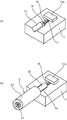
- (First embodiment) 1 to 5 show a single-channel optical module in which one internal waveguide 16 is formed in one first groove 1a of the first substrates 1 and 3.
- FIG. 1 to 5 an outline of a single-channel optical module will be described first, and then a multi-channel optical module according to the first embodiment of the present invention including the structure of the single-channel optical module will be described. This will be described in detail with reference to FIGS.
- FIG. 1 is a schematic side view of a single-channel optical module.
- 2A to 2C are views showing the first substrate 1 of the light emitting side optical module of FIG. 1
- FIG. 2A is a side sectional view of the first substrate 1
- FIG. 2A is a cross-sectional view taken along the line II in FIG. 2A
- FIG. 2C is a cross-sectional view taken along the line II-II in FIG. 3A and 3B are views showing the first substrate 1
- FIG. 3A is a perspective view of the first substrate 1
- FIG. 3B is a diagram in which an internal waveguide 16 is formed.
- 1 is a perspective view of one substrate 1.
- FIG. 4A and 4B are views showing the first substrate 1, FIG.
- FIG. 4A is a perspective view of the first substrate 1 on which the light emitting element 12a is mounted, and FIG. It is a perspective view of the 1st board
- FIG. 5A is a perspective view of the first substrate 1 to which the holding block 24 is fixed, and
- FIG. 5B is a perspective view of the optical fiber 2.
- an optical module includes a first substrate (mount substrate) 1 on a light emitting side, a first (mount) substrate 3 on a light receiving side, and an optical fiber 2 that optically couples the first substrates 1 and 3.
- the vertical direction (the direction of arrow Y) in FIG. 1 is the vertical direction (height direction)
- the direction orthogonal to the paper surface is the left-right direction (width direction)
- the left side in FIG. It is called the back.
- the first substrates 1 and 3 must have heat dissipation and rigidity in order to avoid the influence of heat during mounting and the influence of stress due to the usage environment.
- optical coupling efficiency of a predetermined ratio or more from the light emitting element 12a to the light receiving element 12b is required. Must be suppressed as much as possible.
- a silicon (Si) substrate is employed as the first substrates 1 and 3 in this single channel optical module.
- the first substrate 1 or 3 is a silicon substrate, it is possible to perform highly accurate etching groove processing on the surface using the crystal orientation of silicon. For example, it is possible to form a mirror section 15 and an internal waveguide 16 to be described later using this groove. Moreover, the etching surface of the silicon substrate is excellent in smoothness.
- the first substrates 1 and 3 are respectively installed on the surface (upper surface) of a second substrate (interposer substrate) 6 having a larger size than the first substrates 1 and 3.
- Connectors 7 for electrically connecting to other circuit devices are attached to the back surface (lower surface) of each second substrate 6.
- a light emitting element 12a for converting an electrical signal into an optical signal is flip-chip mounted with bumps 12c (see FIG. 2) with the light emitting surface facing downward.
- An IC substrate (signal processing unit) 4a for transmitting an electrical signal to the light emitting element 12a is mounted on the surface of the second substrate 6.
- a surface emitting laser [VCSEL (Vertical Cavity Surface Emitting Laser)] that is a semiconductor laser is employed as the light emitting element 12a.
- the light emitting element 12a may be an LED or the like.
- the IC substrate 4a is a driver IC that drives the VCSEL, and is disposed in the vicinity of the light emitting element 12a.
- the light emitting element 12a and the IC substrate 4a are connected to a metal circuit (patterning circuit by copper or gold sputtering) and a gold wire formed on the surface of the first substrate 1.
- Two grooves 1b are formed continuously in the front-rear direction.
- an optical path changing mirror 15 for bending the optical path by 90 degrees is formed at a position directly below the light emitting element 12a.
- an internal waveguide 16 that is optically coupled to the light emitting element 12a of the first substrate 1 is provided.
- the internal waveguide 16 extends from the mirror portion 15 in the direction of the second groove 1b, and the end surface of the internal waveguide 16 is flush with the rear end portion 1d of the first groove 1a or on the mirror portion 15 side. It is a little backward.
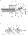
- the internal waveguide 16 includes a core portion 17 having a substantially square cross section with a high refractive index through which light propagates, and a cladding portion 18 having a refractive index lower than that. As shown in FIG. 2C, the left and right surfaces of the core portion 17 are covered with the cladding portion 18. Although not shown, the upper surface of the core portion 17 is also thinly covered with the cladding portion 18.
- a light emitting element 12a is mounted at a predetermined position on the surface of the first substrate 1 on which the internal waveguide 16 is provided.
- the space between the light emitting element 12a and the core portion 17 is filled with an adhesive optical transparent resin (underfill material) 13 as shown in FIG.
- a plurality of mounting substrates 1 are simultaneously formed using a silicon wafer (silicon substrate), and finally the silicon wafer is cut to separate the mounting substrates 1 shown in FIG. 3 one by one.
- a silicon wafer one having a selected crystal orientation is prepared for etching in the next process.
- a 45 ° inclined surface for forming the first groove (waveguide forming groove) 1a and the mirror portion 15 is formed on the silicon wafer. These are formed by anisotropic etching utilizing the difference in etching rate of silicon crystals. In order to form the 45 ° inclined surface, the etching mask shape, the etchant concentration, and the composition are adjusted. In addition to anisotropic etching, there is a dry etching forming method such as reactive ion etching as a method for forming the first groove 1a.
- the cross-sectional shape of the first groove 1a is substantially trapezoidal, and the groove width of the first groove 1a is increased. Since the first groove 1a is not a problem unless it is attached to the bonding pad for the light emitting element 12a to be formed in the next process, it is also possible to do this.
- the second groove 1b can be formed by the anisotropic etching, but the second groove 1b may be formed simultaneously with the formation of the first groove 1a or may be performed separately from the first groove 1a. .
- a wiring pattern (not shown) for mounting the light emitting element 12a is formed on the silicon wafer. Wiring is performed by depositing gold on a silicon wafer and patterning the gold. At this time, gold is also vapor-deposited on the 45 ° inclined surface to form the mirror portion 15. Although depending on the wavelength to be used, it is possible to use the 45 ° inclined surface as it is as the mirror part 15 without depositing gold on the 45 ° inclined surface. For example, when using a near infrared light source, If gold is vapor-deposited on a 45 ° inclined surface, the reflectance increases and the optical coupling efficiency increases.
- a multilayer structure such as titanium, nickel, gold, aluminum or chromium, nickel, gold or the like is formed on the mounting substrate as a wiring material from the viewpoint of ease of solder mounting in the subsequent process and connection reliability.
- the thickness when forming the multilayer structure is, for example, 0.5 ⁇ m, 1 ⁇ m, and 0.2 ⁇ m, respectively.
- an internal waveguide 16 is formed in the first groove 1a.
- the core material is applied on the first substrate 1, and the core material is flattened on the first substrate 1 using a flat mold. Thereafter, only the core portion is irradiated with ultraviolet rays using a mask to cure the core portion, and unnecessary portions other than the core portion are developed and removed.
- a clad material having a refractive index lower than that of the core material is applied to the first groove 1a in which the core portion is formed, and the clad material is flattened on the first substrate 1 like the core material.
- the clad material is hardened by using a mask to shield the first groove 1a from being irradiated with ultraviolet rays.
- the mask is adjusted so as to cure only the region covering the outer periphery of the core portion, and is designed so that the clad material does not cover the circuit of the mounting portion of the optical element 12a.
- the light emitting element 12a is mounted on the silicon wafer as shown in FIGS. 4 (a) and 4 (b). Bumps are formed on the light emitting element 12a by stud bump bonding, and the silicon wafer and the light emitting element 12a are heated to 200 ° C. to perform ultrasonic bonding.
- an underfill material is filled between the light emitting element 12a and the first substrate 1 to reinforce the bonding strength between the light emitting element 12a and the first substrate 1.
- the funder fill material also has an effect of eliminating the air layer between the optical element and the internal waveguide and increasing the optical coupling efficiency.
- the first substrate 1 on which the light emitting element 12 a is mounted is mounted on the surface (upper surface) of the second substrate 6, and the IC substrate 4 a is mounted.
- a connector 7 is attached to the lower surface.
- the light emitting element 12a is mounted on the upper surface of the first substrate 1 mounted on the upper surface of the second substrate 6, and the IC substrate 4a is mounted on the upper surface of the second substrate 6.
- the connector 7 is mounted on the lower surface thereof.
- the light emitting element 12a is mounted on the first substrate 1, not the second substrate 6 on which the IC substrate 4a is mounted, and the mirror portion 15 and the internal waveguide 16 are formed. As a result, the thermal influence from the IC substrate 4a hardly reaches the light emitting element 12a, and the light emission characteristics are stabilized.
- the basic structure of the first substrate 3 on the light receiving side is the same as that of the first substrate 1 on the light emitting side.
- the light receiving element 12b for converting an optical signal into an electrical signal is flip-chip mounted with bumps with the light receiving surface facing downward, so that the first substrate on the light receiving side. 3 is different from the first substrate 1 on the light emitting side.
- the second substrate 6 is different from the second substrate 6 on the light emitting side in that an IC substrate (signal processing unit) 4b that receives an electrical signal from the light receiving element 12b is mounted on the surface of the second substrate 6 on the light receiving side.
- PD Photo Diode
- the IC substrate 4b is an element such as a TIA (Trans-impedance Amplifier) that performs current / voltage conversion.
- the first substrate 1 on the light emitting side, the first substrate 3 on the light receiving side, and the IC substrates 4a and 4b are respectively shielded by a shield case 8 attached to the surface of the second substrate 6.
- the optical fiber 2 passes through the through hole 8 a of the shield case 8.
- the optical fiber 2 includes a core portion 17 of the internal waveguide 16 of the first substrate 1 on the light emitting side and a core portion 17 of the internal waveguide 16 of the first substrate 3 on the light receiving side.
- An optically connectable fiber core portion 21 is provided inside.
- it is a cord type comprised by the fiber cladding part 22 surrounding the outer periphery of this fiber core part 21, and the coating
- the fiber core portion 21, the fiber clad portion 22, and the covering portion 23 are arranged concentrically, and the optical fiber 2 constituted by these has a circular cross section.
- the optical fiber 2 functions as an external waveguide that transmits light outside the first substrate 1.
- the optical fiber 2 passes through the through hole 8a of the shield case 8 as shown in FIG. And the coating
- the fiber clad portion 22 of the optical fiber 2 is installed in the second groove 1b of the first substrate 1.
- FIG. The fiber clad part 22 is positioned by the rising slope part 10d (see FIG. 2A) at the boundary with the first groove 1a.
- the optical axis of the core portion 17 of the internal waveguide 16 of the first substrate 1 and the optical axis of the fiber core portion 21 of the optical fiber 2 are optically coupled in a positioned state.
- the gap between the end face of the core portion 17 of the internal waveguide 16 of the first substrate 1 and the end face of the fiber core portion 21 of the optical fiber 2 is in the range of 0 to 200 ⁇ m.
- the preferred range depends on the size of the cores 17 and 21, but in general, the gap is preferably 0 to 60 ⁇ m.
- a presser block 24 is arranged on the upper portion of the fiber cladding portion 22 of the optical fiber 2 as shown in FIGS. 2 (a) and 5.
- the space between the presser block 24 and the second groove 1b is filled with the adhesive 14.
- the portion of the optical fiber 2 on the distal end side of the fiber clad portion 22 is pressed against the second groove 1b by the press block 24.
- This tip side portion is fixed to the first substrate 1 by the adhesive 14 together with the presser block 24.
- the internal waveguide 16 including the core portion 17 and the clad portion 18 is provided in the first groove 1 a of the first substrate 1. Further, the fiber core portion 21 of the optical fiber 2 installed in the second groove 1 b of the first substrate 1 is optically connected to the core portion 17 of the internal waveguide 16. Then, in the first substrate 1 on the light emitting side in which the optical element is the light emitting element 12a, an optical signal is emitted to the core part 17 of the internal waveguide 16 through the mirror part 15, and the light receiving side in which the optical element is the light receiving element 12b. In the first substrate 3, the optical signal from the core portion 17 of the internal waveguide 16 is received via the mirror portion 15.
- the internal waveguide 16 is interposed between the tip of the fiber core portion 21 of the optical fiber 2 and the mirror portion 15, the light beam emitted from the light emitting element 12a does not spread, and the optical fiber 2 The luminous flux emitted from the fiber core portion 21 does not spread. Therefore, the optical signal transmission loss between the tip of the fiber core portion 21 of the optical fiber 2 and the mirror portion 15 is almost eliminated, and the optical coupling efficiency is improved.
- the core portion 17 has a width as shown in FIG.
- the core portion 17 of the internal waveguide 16 is patterned (photocured), unnecessary reflection on the bottom surface is eliminated. Therefore, in this case, a highly accurate core shape can be obtained.
- FIG. 6A is a plan view of the first substrate 1
- FIG. 6B is an enlarged plan view of the first grooves 1a-1 and 1a-2 and the internal waveguides 16-1 and 16-2 of the first substrate 1.
- FIG. It is.
- the clad portion 18 is hatched for easy understanding of the range of the clad portion 18.
- 7A is an enlarged sectional view taken along the line III-III in FIG. 6A
- FIG. 7B is an enlarged sectional view taken along the line IV-IV in FIG. 6A.
- the multi-channel optical module according to the first embodiment of the present invention shown in FIGS. 6 to 7 includes two single-channel optical modules shown in FIGS. 1 to 5 described above. Specifically, it is as follows.
- a plurality of substantially trapezoidal first grooves 1a-1 and 1a-2 are in an independent state (that is, separated from each other or In other words, the plurality of adjacent first grooves 1a-1 and 1a-2 are formed substantially in parallel with each other being partitioned by the partition wall portion 1e.
- the adjacent first grooves 1a-1 and 1a-2 have lengths L1 and L2 from the end face of the first substrate 1 (the rear end 1d of the first groove 1a in the examples shown in FIGS. 6 to 7). Is different.
- internal waveguides 16-1 and 16-2 are respectively provided as described above.
- the optical elements are placed on the surface of the first substrate 1 so as to face the mirror portions 15 formed at the tip portions of the first grooves 1a-1 and 1a-2 having different lengths.
- the mirror portion 15 disposed at the end of the long internal waveguide 16-1 having the length L1 and the light receiving element 12b face each other, and have a length L2 shorter than the length L1.
- the mirror portion 15 disposed at the end of the short internal waveguide 16-2 and the light emitting element 12a face each other.
- first grooves 1a-1 and 1a-2 are not limited to two, and three or more may be formed. In this case, the lengths of the three adjacent first grooves may be different, and the lengths of the first and third first grooves may be equal. Similarly, in the case of having four or more first grooves, the first grooves that are not adjacent to each other may have the same length.
- two second grooves 1b-1 and 1b-2 are formed on the surface of the first substrate 1.
- the second groove may be substantially trapezoidal or V-shaped if it does not contact the bottom surface of the optical fiber.
- the adjacent second grooves 1b-1 and 1b-2 are partitioned by a partition wall portion 1f.
- the partition wall portion 1f is formed between the first grooves 1a-1 and 1a-2 at an inclined portion 1h between the bottoms of the second grooves 1b-1 and 1b-2 and the bottoms of the first grooves 1a-1 and 1a-2. This is disconnected from the partition wall portion 1e.
- the optical fiber (external waveguide) 2 includes two parallel fiber core portions that can be optically coupled to the core portions 17 of the internal waveguides 16-1 and 16-2. 21 (multiple channels), and the outer periphery of each fiber core portion 21 is surrounded by a fiber cladding portion 22.
- a multi-channel film-like flexible waveguide that is, a flexible waveguide film (external waveguide) can be used.
- the optical axes of the core portions 17 of the internal waveguides 16-1 and 16-2 and the optical fiber 2 are set so as to coincide with each other.
- the lengths L1 and L2 of the adjacent first grooves 1a-1 and 1a-2 of the first substrate 1 are different.
- the optical elements (the light emitting element 12a and the light receiving element 12b) are arranged on the first substrate 1 so as to face the mirror portions 15 at the tips of the first grooves 1a-1 and 1a-2 having different lengths L1 and L2. Mounted on the surface. Thereby, a large distance (space) S (see FIG. 6A) can be separated between adjacent optical elements (light emitting element 12a and light receiving element 12b) that are in different positions in the length direction. .
- the optical element particularly the light leaked from the light emitting element 12a, or the reflected scattered light from the mirror part 15 or the internal waveguide 16-2 is adjacent to the optical element, particularly the mirror part 15 or the internal waveguide 16- of the light receiving element 12b. 1 is difficult to get into. Thereby, even if an optical path is formed with a narrow pitch, crosstalk noise is less likely to occur.
- the internal waveguides 16-1 and 16-2 are provided in a plurality of (two in this example) first grooves 1a-1 and 1a-2 that are formed in an independent state and substantially parallel to each other. Therefore, the internal waveguides 16-1 and 16-2 do not interfere with each other by the partition wall portion 1e of the adjacent first grooves 1a-1 and 1a-2.
- the plurality of optical elements (the light emitting element 12a and the light receiving element 12b) are mounted on the first substrate 1 so as to be close to each other in the width direction of the first substrate 1, and the optical element (the light emitting element 12a and the light receiving element) is mounted. 12b), the internal waveguides 16-1 and 16-2 are formed at a narrow pitch, and the mirror portions 15 at the ends of the internal waveguides 16-1 and 16-2 are formed at a narrow pitch.
- the internal waveguides 16-1 and 16-2 are formed at a narrow pitch
- the mirror portions 15 at the ends of the internal waveguides 16-1 and 16-2 are formed at a narrow pitch.
- the adjacent optical elements (the light emitting element 12a and the light receiving element 12b) are separated by a large distance S, and interference between the adjacent internal waveguides 16-1 and 16-2 is prevented by the partition wall portion 1e. As a result, crosstalk noise can be greatly reduced.
- the light emitting element 12a when both the light emitting element 12a and the light receiving element 12b are included as optical elements, the light emitting element 12a has a length in which the light receiving element 12b is optically coupled. It is mounted on the surface of the first substrate 1 so as to face the mirror portion 15 of the internal waveguide 16-2 having a shorter length L2 than the long internal waveguide 16-1 having L1.
- the light emitting element 12a is arranged on the end surface of the first substrate 1 (in this example, the rear end 1d of the first groove 1a) with respect to the light receiving element 12b.
- the reflected and scattered light of the mirror part 15 on the light emitting element 12a side hardly affects the light receiving element 12b side due to the orientation of the mirror part 15 on the light emitting element 12a side. Therefore, even if both the light emitting element 12a and the light receiving element 12b are mounted on the first substrate 1, the crosstalk noise can be greatly reduced.
- second grooves 1b-1 and 1b-2 are formed which are continuous with the first grooves 1a-1 and 1a-2 of the internal waveguides 16-1 and 16-2.
- the fiber clad portions 22 of the optical fiber 2 are fitted and fixed in the second grooves 1b-1 and 1b-2, respectively, so that the optical axes of the core portions 17 of the internal waveguides 16-1 and 16-2
- the optical axes of the fiber core portions 21 of the optical fiber 2 are matched.
- first grooves 1a-1 and 1a-2 and the second grooves 1b-1 and 1b-2 into which the fiber clad portions 22 of the optical fiber 2 are fitted in the first substrate 1
- Optical coupling between the internal waveguides 16-1 and 16-2 and the optical fiber 2 is facilitated.
- the optical assembly is further facilitated by matching the pitch of the internal waveguides 16-1 and 16-2 with the pitch of the off-the-shelf optical fiber 2.
- An optical module can be manufactured at low cost.
- the optical assembly can be performed by adjusting the pitch of the internal waveguides 16-1 and 16-2 to the pitch of the ready-made flexible waveguide film. It becomes easy and an optical module can be manufactured at low cost.
- the partition wall portion 1g between the adjacent second grooves 1b-1 and 1b-2 is adjacent to the adjacent first groove 1a-.
- the partition wall portion 1e between 1 and 1a-2 is formed so as not to be interrupted.
- the partition wall portion 1g is formed between the adjacent second grooves 1b-1 and 1b-2. Yes. According to this, since the leaked light does not interfere with the adjacent waveguide at the optical coupling portion between the internal waveguides 16-1 and 16-2 and the optical fiber 2, the crosstalk noise can be further reduced. .
- FIG. 9 (a) and FIG. 9 (b) show another modification of the first embodiment of the present invention.
- FIG. 9A is a plan view of the substrate 1 according to the modification
- FIG. 9B is an enlarged cross-sectional view taken along the line VV of FIG. 9A.
- a convex layer 26 containing the same material as the material of the clad portion 18 of the internal waveguide 16 is formed.
- a convex layer 26 containing the same material as the material of the clad portion 18 is formed on the surface of the first substrate 1 between the light emitting element 12a and the light receiving element 12b, whereby the space between the light emitting element 12a and the light receiving element 12b.
- the light leak can be trapped. Therefore, it is possible to further reduce crosstalk noise.
- the convex layer 26 can also be used as a flow stop for the underfill material, which is the optical transparent resin 13 filled between the light emitting element 12 a, the light receiving element 12 b, and the surface of the first substrate 1.
- the material of the convex layer 26 is not limited to the same material as that of the clad portion 18, but if it is the same material, it can be simultaneously formed in the formation process of the clad portion 18.
- an absorber that absorbs light is used as the material of the convex layer 26 instead of the material of the clad portion 18, leakage light between the light emitting element 12a and the light receiving element 12b can be absorbed. Can be reduced.
- the absorber there is a colored resin, for example, an opaque acrylic resin or epoxy resin.
- the optical module according to the first embodiment includes a substrate having a plurality of first grooves formed on the surface, an internal waveguide provided in each of the plurality of first grooves and having a core portion, Mounted on the surface of the substrate so as to be opposed to the mirror part, and a mirror part for optical path conversion formed at the tip part of each of the plurality of first grooves, and through the mirror part,
- An optical element that emits an optical signal to the core part or receives an optical signal from the core part of the internal waveguide through the mirror part, and the plurality of first grooves of the substrate are substantially in an independent state.
- the lengths from the end face of the substrate in the adjacent first grooves formed in parallel are different from each other.
- the optical elements are respectively mounted on the surface of the substrate so as to face the mirror portions formed at the tip portions of the first grooves having different lengths.
- the optical elements by mounting the optical elements on the surface of the substrate so that the lengths of the adjacent first grooves are different from each other and face the mirror part at the tip of the first groove having different lengths, respectively.
- the relationship between the positions different from each other in the length direction for example, a large distance can be provided between adjacent optical elements that are staggered.
- the plurality of internal waveguides are provided in the first grooves formed in an independent state and substantially in parallel, the internal waveguides do not interfere with each other at the partition wall portions of the adjacent first grooves.
- the plurality of optical elements are mounted on the substrate in the vicinity of the width direction of the substrate, and the internal waveguide and the mirror portion are narrowed so that the pitch of the internal waveguide and the pitch of the mirror portion is reduced according to the interval of the optical elements.
- the mirror portion By forming the mirror portion, it is possible to transmit in a bidirectional manner or a plurality of channels with a small size and a low height.
- crosstalk noise can be greatly reduced by separating a large distance between adjacent optical elements and preventing interference between adjacent internal waveguides.
- the plurality of optical elements include both a light emitting element and a light receiving element, and the light emitting element has a tip that is shorter than an internal waveguide optically coupled to the light receiving element. It can be set as the structure mounted in the said surface of the said board
- the reflected and scattered light of the mirror part on the light emitting element side is directed to the light receiving element side in relation to the orientation of the mirror part on the light emitting element side. It becomes difficult to influence. Therefore, even if both the light emitting element and the light receiving element are mounted on the substrate, the crosstalk noise can be greatly reduced.
- An optical module includes an external waveguide having a core portion optically coupled to the core portion of the internal waveguide, and a second groove connected to the first groove of the internal waveguide is formed on the surface of the substrate. Is formed, and the external waveguide is fitted and fixed in the second groove, whereby the optical axis of the internal waveguide and the optical axis of the external waveguide are set to coincide with each other.
- the optical coupling between the internal waveguide and the external waveguide becomes easy, and the cost is low and high.
- An accurate optical module can be manufactured.
- the partition wall portion may be formed between the adjacent second grooves so that the partition wall portion between the adjacent first grooves is not interrupted.
- the optical module may include an external waveguide having a core portion optically coupled to the core portion of the internal waveguide, and the external waveguide may be a multi-channel optical fiber.
- optical assembly becomes easy, and an optical module can be manufactured at low cost.
- the optical module includes an external waveguide having a core portion optically coupled to the core portion of the internal waveguide, and the external waveguide is a multi-channel flexible waveguide film. it can.
- the optical assembly becomes easy and an optical module can be manufactured at low cost.
- a convex layer containing the same material as the material of the cladding portion of the internal waveguide can be formed on the surface of the substrate between the optical elements.
- the convex layer containing the same material as the material of the clad portion having a high refractive index is formed on the surface of the substrate between the optical elements, the leakage light between the optical elements can be trapped. Can be further reduced.
- the convex layer can also be used as a flow stopper for the underfill material filled between the optical element and the surface of the substrate.
- the convex layer may be configured to be an absorber that absorbs light.
- the absorber is formed on the surface of the substrate between the optical elements, leakage light between the optical elements can be absorbed, so that crosstalk noise can be further reduced.
- a plurality of second grooves having a substantially V-shaped cross section deeper than the plurality of first grooves are formed continuously with the first groove, and the external waveguide is formed in the second groove.
- an optical fiber having a fiber core part which is the core part of the external waveguide and a fiber clad part installed in the external waveguide.
- a plurality of second grooves having a substantially V-shaped cross section deeper than the plurality of first grooves are formed continuously with the first grooves, and are installed in the second grooves of the substrate.
- the fiber core portion of the optical fiber is optically connected to the core portion of the internal waveguide.
- both of the light flux emitted from the light emitting element and the light flux emitted from the fiber core portion of the optical fiber Does not spread. Accordingly, optical signal transmission loss between the tip of the fiber core portion of the optical fiber and the mirror portion is almost eliminated, and the optical coupling efficiency is improved.
- a second groove having a V-shaped cross section into which the optical fiber 2 functioning as an external waveguide is fitted is formed on the surface of the substrate.
- the second groove having a trapezoidal cross-sectional shape that is, a second groove having a bottom surface having a predetermined width and two inclined surfaces at both ends of the bottom surface, as in the second embodiment described below. You may employ
- the configuration of the single-channel optical module shown in FIGS. 10 to 14 as the second embodiment includes the second groove 1b having a trapezoidal cross-sectional shape. Unlike the configuration of the optical module having the second groove 1b having the V-shaped cross section shown in FIG. 2, the configuration is the same in other respects, and thus the description of the common configuration is omitted.
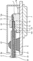
- the surface (upper surface) of the first substrate 1 has a substantially trapezoidal cross section as shown in FIG.
- One groove (waveguide forming groove) 1a and a substantially trapezoidal second groove 1b deeper than the first groove 1a are formed continuously in the front-rear direction.
- the second groove 1b includes a bottom surface 10f formed with a predetermined width, and an outer periphery of a fiber cladding portion 22 of the optical fiber 2 described later. And two inclined surfaces 10e that abut against and support the optical fiber 2. These inclined surfaces 10e are respectively connected to both ends of the bottom surface 10f in the width direction, and from each of the both ends, the distance from each other gradually increases toward the upper side of the first substrate 1 toward the upper side. It extends to the surface (ie, the top surface). When the outer periphery of the fiber clad portion 22 of the optical fiber 2 is in contact with these inclined surfaces 10e, the fiber clad portion 22 can be centered.
- the bottom surface 10f is formed so as not to be in contact with the outer periphery of the fiber clad portion 22 when the inclined surface 10e contacts the outer periphery of the fiber clad portion 22 of the optical fiber 2.
- an internal waveguide 16 composed of a core portion 17 and a cladding portion 18 is provided in the first groove 1a of the first substrate 1 as in the optical module of the first embodiment.
- the fiber core portion 21 of the optical fiber 2 installed in the second groove 1 b of the first substrate 1 is optically connected to the core portion 17 of the internal waveguide 16.
- an optical signal is emitted to the core part 17 of the internal waveguide 16 through the mirror part 15, and the light receiving side in which the optical element is the light receiving element 12b.
- the optical signal from the core portion 17 of the internal waveguide 16 is received via the mirror portion 15.
- the internal waveguide 16 is interposed between the tip of the fiber core portion 21 of the optical fiber 2 and the mirror portion 15, the light beam emitted from the light emitting element 12a does not spread, and the optical fiber 2 The luminous flux emitted from the fiber core portion 21 does not spread. Therefore, the optical signal transmission loss between the tip of the fiber core portion 21 of the optical fiber 2 and the mirror portion 15 is almost eliminated, and the optical coupling efficiency is improved.
- the core portion 17 of the internal waveguide 16 can be formed at the time of molding the core portion 17.
- patterning photocuring
- unnecessary reflection on the bottom surface is eliminated. Therefore, in this case, a highly accurate core shape can be obtained.
- the first groove 1a which is the waveguide forming groove of the first substrate 1
- the core portion 17 has a substantially square cross section.
- the left and right surfaces of the core portion 17 are covered with the clad portion 18.
- the internal waveguide 16 is not limited to this type.
- the first groove 1a of the first substrate 1 has a shallower cross-sectional shape than the second groove 1b and has a substantially V-shape.
- the core portion 17 may be formed in a substantially pentagonal cross-sectional shape adapted to the first groove 1a, and both the left and right sides of the core portion 17 may be covered with the clad portion 18.
- the core part 17 should just be formed in cross-sectional substantially pentagon shape so that it may have an upper surface, a pair of parallel side surface, and a V-shaped lower surface.
- the core portion 17 having a substantially inverted triangular cross section may be formed by filling the entire inside of the first groove 1 a where the silicon oxide film 40 functioning as the cladding portion 18 is formed with the core resin.
- the fiber core portion 21 may not be reached.
- the width W1 of the core portion 17 by making the width W1 of the core portion 17 substantially the same as the width W2 of the fiber core portion 21, almost all of the luminous flux is made to be the fiber core portion 21 of the optical fiber 2. As a result, the optical coupling efficiency is improved.
- the width W1 of the core portion 17 does not necessarily have to be substantially the same as the width W2 of the fiber core portion 21, and may be narrower than the width W3 of the upper end of the first groove 1a. These are the same even when the core portion 17 has a substantially square cross section as shown in FIG.
- the core portion 17 of the internal waveguide 16 is connected to the optical fiber 2 from the mirror portion 15 as shown in FIGS. 19 (a) and 19 (b). It is possible to form a sloped shape so that the width W of the core portion 17 (distance between both side surfaces 17a) gradually decreases linearly toward the connection end with the fiber core portion 21. Further, the both side surfaces 17a are formed as slopes composed of a plurality of planes having different inclination angles as shown in FIG. 19C, or curved surfaces as shown in FIG. 19D. It can also be formed in a slope shape.
- the core portion 17 of the internal waveguide 16 is a fiber of the optical fiber 2 as shown in FIGS. 20 (a) and 20 (b). It can be formed in a slope shape so that the width W of the core portion 17 (distance between both side surfaces 17a) gradually decreases linearly from the connecting end portion with the core portion 21 toward the mirror portion 15. Further, the both side surfaces 17a are formed as slopes composed of a plurality of planes with different inclination angles as shown in FIG. 20 (c), or curved surfaces as shown in FIG. 20 (d). It can also be formed in a slope shape.
- the core portion 17 of the internal waveguide 16 is tapered (that is, the shape becomes narrower toward the front), and is emitted from the light emitting element 12a.
- the luminous flux is converged.
- the core part 17 of the internal waveguide 16 is narrowed backward (that is, a shape that becomes narrower toward the rear) to be emitted from the fiber core part 21 of the optical fiber 2. Converged light flux. Accordingly, in any case, the optical coupling efficiency is further improved.
- the surface (upper surface) of the first substrate 1 has a substantially cross-sectional shape that is continuous with the second groove 1b and deeper than the second groove 1b.
- a third groove 1c having a shape is formed.
- the covering portion 23 of the optical fiber 2 can be installed in the third groove 1c.
- the third groove 1c of the second embodiment includes a bottom surface 10h formed with a predetermined width, and two inclined surfaces 10g that contact the outer periphery of the covering portion 23 of the optical fiber 2 and support the optical fiber 2. It has.
- the inclined surfaces 10g of the third grooves are respectively connected to both ends in the width direction of the bottom surface 10h of the third groove 1c so as to gradually increase from both ends as the distance from each other increases. It extends to the surface of the first substrate 1 toward the upper side.
- the bottom surface 10 h and the inclined surface 10 g of the third groove 1 c are formed so as to be out of contact with the outer periphery of the covering portion 23 of the optical fiber 2.
- the clad portion 22 of the optical fiber 2 can be installed in the second groove 1b of the first substrate 1, but also the covering portion 23 of the optical fiber 2 can be installed in the third groove 1c of the first substrate 1. Therefore, it is possible to prevent stress from the optical fiber 2 from being concentrated on the boundary portion between the fiber clad portion 22 and the coating portion 23.
- the covering part 23 is bonded and fixed to the third groove 1c with an adhesive, the fixing strength of the optical fiber 2 is improved. Even if a bending force or a pulling force is applied to the optical fiber 2 from the outside of the module, the optical coupling efficiency with the internal waveguide 16 is not affected, so that the optical coupling efficiency does not decrease.
- the covering portion 23 when the covering portion 23 is not bonded and fixed to the third groove 1c, as shown in FIG. 21, an adhesive that is built up on the surface of the second substrate 6 (that is, provided so as to protrude upward). 20, the covering portion 23 of the optical fiber 2 can be fixed to the second substrate 6.
- the covering portion 23 of the optical fiber 2 can be installed and fixed on the second substrate 6, so that the fixing strength of the optical fiber 2 is improved. Further, even if a bending force or a pulling force acts on the optical fiber 2 from the outside of the module, the optical coupling efficiency with the internal waveguide 16 is not affected, so that the optical coupling efficiency does not decrease. Furthermore, if a structure in which the covering portion 23 of the optical fiber 2 is installed and fixed in the third groove 1c of the first substrate 1 is used in combination, the fixing strength is further improved.
- the covering portion 23 and the covering body 25 of the optical fiber 2 are fixed to the second substrate 6 with the adhesive 20. can do.
- the covering 25 is not limited to the one fitted into the covering 23 as long as it covers the outer periphery of the covering 23.
- the covering 25 may be bonded at the third groove 1c portion of the first substrate 1 (not shown).
- the covering portion 23 is a layer having a thickness of about 5 to 100 ⁇ m formed of, for example, a UV curable resin, and the covering body 25 is made of, for example, PVC, nylon, or a thermoplastic polyester elastomer (for example, Hytrel (registered trademark)). It is formed.
- the outer diameter of the covering 25 is, for example, about 900 microns in the case of a single-core optical fiber.
- the covering 25 can be installed on the second substrate 6 and fixed to the second substrate 6 together with the covering portion 23 of the optical fiber 2.
- the fixing strength of the optical fiber 2 is improved.
- the optical coupling efficiency with the internal waveguide 16 is not affected, so that the optical coupling efficiency does not decrease.
- the fixing strength is further improved.
- the bending of the optical fiber 2 due to its own weight can be suppressed by the thickness of the covering 25, and an external force is hardly applied to the bonded portion between the optical fiber 2 and the substrate 1.
- stress is unlikely to occur in the optical coupling portion between the optical fiber 2 and the internal waveguide 16, so that the optical coupling efficiency is unlikely to decrease.
- the optical coupling efficiency is good when the inclination angle of the mirror portion 15 is 45 degrees.
- the first groove 1a and the second groove 1b can be formed by anisotropic etching of silicon. According to this, groove processing utilizing the crystal orientation of silicon is possible, the first groove 1a can form a highly accurate mirror shape, and the second groove 1b can reduce misalignment of the installation of the optical fiber 2. Can do.
- a photosensitive resin can be used as the material of the internal waveguide 16. According to this, compared with the inorganic internal waveguide formed repeatedly by ion doping or deposition, it is cheap and easy to form.
- a silicon oxide film can be formed on the surface of the first substrate 1 including the inside of the first groove 1a, so that the refractive index of the core portion 17 of the internal waveguide 16 can be made larger than that of the silicon oxide film. According to this, the internal waveguide 16 can be easily formed by filling the first groove 1 a with the material that becomes the core portion 17 of the internal waveguide 16.
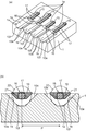
- a plurality of first grooves 1a and a plurality of second grooves 1b are formed.
- One groove 1a is arranged in parallel to each other, and a plurality of second grooves 1b are also arranged in parallel to each other.
- the surface of the first substrate 1 has a plurality of trapezoidal cross sections as shown in FIG. 23 (a).
- the first grooves (waveguide forming grooves) 1 a are arranged in parallel in a state where they are separated from each other by the material of the first substrate 1.
- the lengths of the plurality of first grooves 1a are set so that the lengths of the adjacent first grooves 1a are different as in the first embodiment.
- a plurality of second grooves 1b having a substantially trapezoidal cross-sectional shape deeper than the first groove 1a are formed on the surface of the first substrate 1 continuously in the front-rear direction from the end of each first groove 1a. ing.
- an optical path conversion mirror 15 is formed at the tip of each first groove 1a.
- an internal waveguide 16 that is optically coupled to the light emitting element 12a corresponding to each first groove 1a.
- the internal waveguide 16 includes a core portion 17 having a substantially square cross section with a high refractive index through which light propagates, and a cladding portion 18 having a refractive index lower than that. As shown in FIG. 23B, the left and right surfaces (both side surfaces) of the core portion 17 are covered with the cladding portion 18. Further, the clad portion 18 is thinly covered on the upper surface of the core portion 17.
- Each of the second grooves 1b shown in FIGS. 23 (a) and 23 (b) supports the bottom surface 10f formed with a predetermined width and the outer periphery of the fiber clad portion 22 of the optical fiber 2.
- Two inclined surfaces 10e These inclined surfaces 10e are respectively connected to both ends of the bottom surface 10f in the width direction, and from each of the both ends, the distance from each other gradually increases toward the upper side of the first substrate 1 toward the upper side. It extends to the surface (ie, the top surface).
- the bottom surface 10f is formed so as not to be in contact with the outer periphery of the fiber clad portion 22 when the inclined surface 10e contacts the outer periphery of the fiber clad portion 22 of the optical fiber 2.
- each of the first grooves 1a is formed. It is possible to suppress leakage (crosstalk) of the optical signal passing through to the adjacent first groove 1a.
- the interval P between the core portions 17 of the adjacent internal waveguides 16 is not particularly limited in the present invention, and can be arbitrarily set.
- the interval P between the core portions 17 may be set to about 250 ⁇ m.
- the size of the second groove 1b is not particularly limited in the present invention. Considering that the outer diameter of the most commonly used thin optical fiber is 125 ⁇ m, the size of the second groove 1 b is the size corresponding to the optical fiber having the outer diameter of the cladding portion 22 of about 125 ⁇ m. It may be set. In order to suppress crosstalk, it is desirable to separate the second groove 1b from the adjacent second groove 1b as shown in FIG.
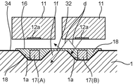
- the entire surface of the substrate 1 that is, the first grooves.
- An oxide film layer 34 is formed on the surface 1a and the entire surface of the partition wall portion 1f.
- the partition wall portion 1 f functioning as a shielding portion is a portion protruding upward between the first grooves 1 a in the substrate 1.
- the partition wall portion 1f shields the scattered component a of the reflected light of the mirror portion 15 between the first grooves 1a from leaking.
- the oxide film layer 34 can reflect the optical signal so as not to leak out of the first groove 1a, and can also suppress the leakage of the scattered component a of the reflected light of the mirror unit 15. According to this configuration, since the oxide film layer 34 becomes a reflection layer that reflects an optical signal, leakage (crosstalk) of the optical signal can be further suppressed. Strictly speaking, an optical signal composed of infrared light or the like has a property of passing through the substrate 1 composed of silicon while being attenuated, but the optical signal is reflected by the oxide film layer 34 as described above. As a result, the crosstalk suppression effect can be improved.
- the gap between the optical element 11 having the light emitting portion 12a and the substrate 1 is exaggerated and enlarged so that the light path can be easily seen. In practice, this gap is very small. And no large crosstalk occurs. The same applies to FIGS. 25 to 26.
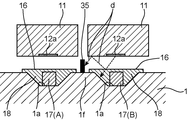
- the optical module shown in FIG. 25 has a structure in which an oxide film layer 34 is formed on the surface of the substrate 1 as shown in FIG.
- the removed portion 32 is formed by partially removing the oxide film layer 34 on the surface of the partition wall portion 1 f protruding in the first place.
- the surface of the partition wall portion 1 f protruding upward from the first substrate 1 is provided along the partition wall portion 1 f.
- a light absorber 35 is disposed.
- the light absorber 35 for example, opaque acrylic or epoxy resin is used. According to this configuration, when the leaked light d that is multiple-reflected between the optical element 11 having the light emitting part 12a and the clad part 18 is generated, the leaked light d is absorbed by the light absorber 35 and the light leakage is prevented. Can be blocked.
- optical element 11 shown in FIGS. 24 to 26 is one in which the light emitting element 12a is separated, but may be one in which the light emitting element 12a and the light receiving element 12b are mounted together.
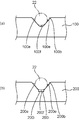
- the bottom surface of the second groove of the first substrate is formed in a planar shape, but the present invention is not limited to this and can be changed as appropriate.
- the bottom surface 100f of the second groove 100b of the first substrate 100 is curved, and the inclined surface 100e is formed from both ends of the curved bottom surface 100f in the width direction. May be formed obliquely upward.
- the bottom surface and the inclined surface of the second groove of the first substrate are directly connected to each other.
- the present invention is not limited to this configuration and can be changed as appropriate.
- the inclined surface 200e and the bottom surface 200f may be indirectly connected via a connecting portion 200i.
- the second groove 200b of the first substrate 200 is provided with connection portions 200i extending in the vertical direction from both ends in the width direction of the bottom surface 200f, and the inclined surfaces 200e are respectively It is assumed that each of the connecting portions 200i is formed obliquely upward.
- the third groove similarly to the second groove, the bottom surface may have a curved shape, and the bottom surface and the inclined surface may be indirectly connected via a connecting portion. Can change.
- the connector 7 is attached to the back surface (lower surface) of the second substrate 6.
- the present invention is not limited to this configuration.
- it can be disposed on the surface (upper surface) of the second substrate 6 and can be appropriately changed.
- the electrical terminal 207 may be disposed on the surface of the second substrate 6.
- another connector 207 a that is detachably fitted to the end of the second substrate 6 is provided with an electrical terminal 207 b that is connected to the electrical terminal 207, and the other connector 207 a is fitted to the second substrate 6.
- the electrical terminal 207 may be connected to the electrical terminal 207b of another connector 207a.
- the optical module according to the second embodiment of the present invention has a substrate in which a plurality of first grooves and a plurality of second grooves deeper than the first groove are continuously formed on the surface;
- An internal waveguide provided in the first groove of the substrate, an optical path conversion mirror provided at the tip of the first groove, and a mirror mounted on the surface of the substrate so as to face the mirror.
- An optical element that emits an optical signal to the core part of the internal waveguide through the part or receives an optical signal from the core part of the internal waveguide through the mirror part, and a clad disposed in the second groove And an optical fiber as an external waveguide having a fiber core portion optically connected to the core portion and the core portion of the internal waveguide, and the second groove has a bottom surface formed with a predetermined width, and a width direction of the bottom surface Connected to both ends of the fiber cladding And a sloped surface for supporting the periphery.
- an internal waveguide having a core portion is provided in the first groove of the substrate, and the fiber core portion of the optical fiber installed in the second groove of the substrate is optically connected to the core portion of the internal waveguide. ing.
- the optical element is a light emitting element
- an optical signal is emitted to the core part of the internal waveguide via the mirror part.
- the optical element is a light receiving element
- the optical element is output from the core part of the internal waveguide via the mirror part. The optical signal is received.
- both of the light flux emitted from the light emitting element and the light flux emitted from the fiber core portion of the optical fiber Does not spread. Therefore, the optical signal propagation loss between the tip of the fiber core portion of the optical fiber and the mirror portion is almost eliminated in any direction, so that the optical coupling efficiency is improved.
- the second groove is configured to have a bottom surface, it is not necessary to deepen the groove and lengthen the inclined surface like a V-shaped cross section. Therefore, for example, when the second groove is formed by etching, the second groove can be easily formed in a short time as compared with the V-shaped cross section.
- the core portion of the internal waveguide is such that when the optical element is a light emitting element, the width of the core portion gradually decreases from the mirror portion toward the connection end portion with the fiber core portion of the optical fiber. It can be set as the structure which has a slope.
- the optical element is a light emitting element
- the light beam emitted from the light emitting element is converged by tapering the core portion of the internal waveguide. Therefore, the optical coupling efficiency is further improved.
- the core portion of the internal waveguide is such that the width of the core portion gradually narrows from the connecting end portion of the optical fiber to the mirror portion when the optical element is a light receiving element. It can be set as the structure which has a slope.
- the optical element is a light receiving element
- the light beam emitted from the fiber core part of the optical fiber is converged by making the core part of the internal waveguide narrower. Therefore, the optical coupling efficiency is further improved.
- the width of the core portion of the internal waveguide may be narrower than the width of the upper end of the first groove.
- the width of the core portion of the internal waveguide is the same as the width of the upper end of the first groove
- the light beam from the optical element spreads in the width direction at the core portion, and a part of the light beam is transferred to the fiber core portion of the optical fiber. May not reach. Therefore, by making the width of the core portion narrower than the width of the upper end of the first groove, preferably substantially the same width as the width of the fiber core portion, almost all of the light beam can reach the fiber core portion of the optical fiber. As a result, the optical coupling efficiency is improved.
- the first groove may have a substantially trapezoidal cross section, and the bottom surface of the first groove may be wider than the core portion of the internal waveguide.
- a third groove deeper than the second groove is formed on the surface of the substrate continuously to the second groove, and the third groove is fixed to the coating portion of the optical fiber. it can.
- the coated portion of the optical fiber can also be installed in the third groove of the first substrate, it is possible to prevent the stress from the optical fiber from concentrating on the boundary portion with the coated portion of the fiber clad portion.
- the third groove has a bottom surface, it is not necessary to deepen the groove and lengthen the inclined surface like a V-shaped cross section.
- the third groove is formed by etching It can be easily formed in a short time as compared with the V-shaped cross section.
- the substrate may be installed on another substrate having a size larger than that of the substrate, and the coating portion of the optical fiber may be fixed to the other substrate.
- the coating portion of the optical fiber can be installed and fixed on another substrate, the fixing strength of the optical fiber is improved. Also, even if bending force or tensile force acts on the optical fiber from the outside of the module, the optical coupling efficiency with the internal waveguide is not lowered because the optical coupling portion with the internal waveguide is not affected.
- the substrate is installed on another substrate having a size larger than that of the substrate, a covering body is fixed to the outer periphery of the coating portion of the optical fiber, and the covering body is fixed to the separate substrate. be able to.
- the covering can be installed and fixed on another substrate, the fixing strength of the optical fiber is improved. Also, even if bending force or tensile force acts on the optical fiber from the outside of the module, the optical coupling efficiency with the internal waveguide is not lowered because the optical coupling portion with the internal waveguide is not affected. In addition, the bending of the optical fiber due to its own weight can be suppressed by the thickness of the covering, and an external force can be suppressed from being applied to the bonded portion of the optical fiber. As a result, stress is hardly generated in the optical coupling portion with the internal waveguide, so that the optical coupling efficiency is not easily lowered.
- each of the plurality of first grooves may be separated from each other and disposed on the substrate.
- the present invention is useful for an optical module including an optical element.
Abstract
Description
図1~図5には、1本の内部導波路16が第1基板1,3の1本の第1溝1a内に形成された単チャンネルの光モジュールが示されている。この図1~図5によって、先ず、単チャンネルの光モジュールの概要を説明し、その後、この単チャンネルの光モジュールの構造を含む本発明の第1実施形態に係る多チャンネルの光モジュールについて、図6~図9で詳細に説明する。 (First embodiment)
1 to 5 show a single-channel optical module in which one
上記第1の実施形態では、基板の表面には、外部導波路として機能する光ファイバー2が嵌め込まれるV字断面形状の第2溝が形成されている例が示されているが、本発明はこれに限定されるものではなく、以下の第2実施形態のように、台形断面形状の第2溝、すなわち、所定の幅を有する底面および当該底面両端の2つの傾斜面を有する形状の第2溝を備えた構造を採用してもよい。 (Second Embodiment)
In the first embodiment, an example in which a second groove having a V-shaped cross section into which the
1a、1a-1,1a-2 第1溝
1b、1b-1,1b-2 第2溝
1c 第3溝
1e,1f,1g 仕切り壁部分
2 光ファイバー(外部導波路)
6 第2基板(別基板)
10e、100e 第2溝の傾斜面
10f、100f 第2溝の底面
12a 発光素子(光素子)
12b 受光素子(光素子)
13 光学透明樹脂
15 ミラー部
16-1,16-2 内部導波路
17 コア部
18 クラッド部
21 ファイバーコア部
22 ファイバークラッド部
23 被覆部
25 被覆体
W1~W3 幅
26 凸形層(吸収体)
L1,L2 長さ 1
6 Second board (separate board)
10e, 100e
12b Light receiving element (optical element)
13 Optical
L1, L2 length
Claims (16)
- 表面に複数の第1溝が形成された基板と、
前記複数の第1溝内にそれぞれ設けられるとともにコア部を有する内部導波路と、
前記複数の第1溝の先端部にそれぞれ形成された光路変換用のミラー部と、
前記ミラー部と対向するように前記基板の前記表面に実装され、前記ミラー部を介して前記内部導波路のコア部に光信号を発光し、若しくは前記ミラー部を介して前記内部導波路のコア部からの光信号を受光する光素子と
を備え、
前記基板の前記複数の第1溝は独立状態で略平行に形成され、隣り合う前記第1溝における前記基板の端面からの長さは互いに異なり、
前記光素子は、この長さの異なる前記第1溝の先端部にそれぞれ形成された前記ミラー部と対向するように、前記基板の前記表面にそれぞれ実装されている、
ことを特徴とする光モジュール。 A substrate having a plurality of first grooves formed on the surface;
An internal waveguide provided in each of the plurality of first grooves and having a core portion;
An optical path changing mirror portion formed at each of the tip ends of the plurality of first grooves;
It is mounted on the surface of the substrate so as to face the mirror part, and emits an optical signal to the core part of the internal waveguide through the mirror part, or the core of the internal waveguide through the mirror part An optical element for receiving an optical signal from the unit,
The plurality of first grooves of the substrate are formed to be substantially parallel in an independent state, and the lengths of the adjacent first grooves from the end face of the substrate are different from each other,
The optical elements are respectively mounted on the surface of the substrate so as to face the mirror portions formed at the tip portions of the first grooves having different lengths.
An optical module characterized by that. - 前記複数個の光素子には、発光素子と受光素子が含まれており、
前記発光素子は、前記受光素子に光学的に結合された前記内部導波路より長さが短い前記内部導波路の先端部に形成されたミラー部と対向するように、前記基板の前記表面に実装されていることを特徴とする請求項1に記載の光モジュール。 The plurality of optical elements include a light emitting element and a light receiving element,
The light emitting element is mounted on the surface of the substrate so as to face a mirror portion formed at a tip portion of the internal waveguide that is shorter than the internal waveguide optically coupled to the light receiving element. The optical module according to claim 1, wherein the optical module is provided. - 前記内部導波路の前記コア部と光学的に結合されるコア部を有する外部導波路をさらに備えており、
前記基板の前記表面に、前記内部導波路の前記第1溝と連なる第2溝が形成され、
前記第2溝に前記外部導波路が嵌め込み固定されることによって、前記内部導波路の光軸と前記外部導波路の光軸が一致するように設定されていることを特徴とする請求項1または2に記載の光モジュール。 An external waveguide having a core portion optically coupled to the core portion of the internal waveguide;
A second groove connected to the first groove of the internal waveguide is formed on the surface of the substrate;
The optical waveguide of the internal waveguide and the optical axis of the external waveguide are set to coincide with each other by fitting and fixing the external waveguide in the second groove. 2. The optical module according to 2. - 前記隣り合う第1溝の間の仕切り壁部分と途切れないように、隣り合う前記第2溝の間に仕切り壁部分が形成されていることを特徴とする請求項3に記載の光モジュール。 The optical module according to claim 3, wherein a partition wall portion is formed between the adjacent second grooves so as not to be interrupted by the partition wall portion between the adjacent first grooves.
- 前記内部導波路の前記コア部と光学的に結合されるコア部を有する外部導波路をさらに備えており、
前記外部導波路は、複数チャンネルの光ファイバーであることを特徴とする請求項1~4のいずれか一項に記載の光モジュール。 An external waveguide having a core portion optically coupled to the core portion of the internal waveguide;
The optical module according to any one of claims 1 to 4, wherein the external waveguide is a multi-channel optical fiber. - 前記内部導波路の前記コア部と光学的に結合されるコア部を有する外部導波路をさらに備えており、
前記外部導波路は、複数チャンネルのフレキシブル導波路フィルムであることを特徴とする請求項1~4のいずれか一項に記載の光モジュール。 An external waveguide having a core portion optically coupled to the core portion of the internal waveguide;
The optical module according to claim 1, wherein the external waveguide is a multi-channel flexible waveguide film. - 前記各光素子の間の基板の表面に、前記内部導波路のクラッド部と同材料の凸形層が形成されていることを特徴とする請求項1~6のいずれか一項に記載の光モジュール。 The light according to any one of claims 1 to 6, wherein a convex layer of the same material as that of the clad portion of the internal waveguide is formed on the surface of the substrate between the optical elements. module.
- 前記内部導波路の前記コア部と光学的に結合されるコア部を有する外部導波路をさらに備えており、
前記基板の前記表面において、前記複数の第1溝よりも深い断面略V字形状の複数の第2溝が当該第1溝と連続して形成され、
前記外部導波路は、前記第2溝内に設置されたファイバークラッド部、および当該外部導波路の前記コア部であるファイバーコア部を有する光ファイバーを備えている、
請求項1に記載の光モジュール。 An external waveguide having a core portion optically coupled to the core portion of the internal waveguide;
On the surface of the substrate, a plurality of second grooves having a substantially V-shaped cross section deeper than the plurality of first grooves are continuously formed with the first grooves,
The external waveguide includes an optical fiber having a fiber clad portion installed in the second groove and a fiber core portion which is the core portion of the external waveguide.
The optical module according to claim 1. - 前記内部導波路の前記コア部と光学的に結合されるコア部を有する外部導波路をさらに備えており、
前記基板の前記表面において、前記複数の第1溝よりも深い複数の第2溝が当該第1溝と連続して形成され、
前記外部導波路は、前記第2溝内に設置されたファイバークラッド部、および当該外部導波路の前記コア部であるファイバーコア部を有する光ファイバーを備えており、
前記第2溝は、所定の幅で形成された底面と、前記底面の幅方向の両端のそれぞれに接続され、前記ファイバークラッド部の外周を支持する傾斜面とを備えていることを特徴とする請求項1に記載の光モジュール。 An external waveguide having a core portion optically coupled to the core portion of the internal waveguide;
On the surface of the substrate, a plurality of second grooves deeper than the plurality of first grooves are continuously formed with the first grooves,
The external waveguide includes an optical fiber having a fiber clad portion installed in the second groove, and a fiber core portion that is the core portion of the external waveguide,
The second groove includes a bottom surface formed with a predetermined width and inclined surfaces that are connected to both ends of the bottom surface in the width direction and support the outer periphery of the fiber clad portion. The optical module according to claim 1. - 前記内部導波路の前記コア部は、前記光素子が発光素子である場合において、前記ミラー部から前記光ファイバーの前記ファイバーコア部との接続端部に向かって、前記コア部の幅が徐々に細くなるような斜面を有することを特徴とする請求項9に記載の光モジュール。 In the core portion of the internal waveguide, when the optical element is a light emitting element, the width of the core portion gradually narrows from the mirror portion toward the connection end portion of the optical fiber with the fiber core portion. The optical module according to claim 9, further comprising an inclined surface.
- 前記内部導波路の前記コア部は、前記光素子が受光素子である場合において、前記光ファイバーの前記ファイバーコア部との接続端部から前記ミラー部に向かって、前記コア部の幅が徐々に細くなるような斜面を有することを特徴とする請求項9に記載の光モジュール。 In the core portion of the internal waveguide, when the optical element is a light receiving element, the width of the core portion gradually narrows from the connection end portion of the optical fiber to the fiber core portion toward the mirror portion. The optical module according to claim 9, further comprising an inclined surface.
- 前記内部導波路の前記コア部の幅は、前記第1溝の上端の幅よりも狭いことを特徴とする請求項9~11のいずれか一項に記載の光モジュール。 The optical module according to any one of claims 9 to 11, wherein a width of the core portion of the internal waveguide is narrower than a width of an upper end of the first groove.
- 前記第1溝は断面形状が略台形状であり、前記第1溝の底面は前記内部導波路の前記コア部よりも幅が広いことを特徴とする請求項9~12のいずれか一項に記載の光モジュール。 The first groove has a substantially trapezoidal cross-sectional shape, and a bottom surface of the first groove is wider than the core portion of the internal waveguide. The optical module as described.
- 前記基板の前記表面に、前記第2溝に連続して、前記第2溝よりも深い第3溝が形成され、
前記第3溝は、前記光ファイバーの被覆部と接着されている請求項9~13のいずれか一項に記載の光モジュール。 A third groove deeper than the second groove is formed on the surface of the substrate continuously to the second groove,
The optical module according to any one of claims 9 to 13, wherein the third groove is bonded to the coating portion of the optical fiber. - 前記基板は、前記基板よりもサイズが大きい別基板に設置され、前記別基板に、前記光ファイバーの被覆部が固定されていることを特徴とする請求項9~14のいずれか一項に記載の光モジュール。 The substrate according to any one of claims 9 to 14, wherein the substrate is installed on another substrate having a size larger than the substrate, and a covering portion of the optical fiber is fixed to the other substrate. Optical module.
- 前記基板は、前記基板よりもサイズが大きい別基板に設置され、前記光ファイバーの被覆部の外周に被覆体が固定されて、前記別基板に、前記被覆体が固定されていることを特徴とする請求項9~15のいずれか一項に記載の光モジュール。 The substrate is installed on another substrate having a size larger than that of the substrate, a covering body is fixed to an outer periphery of the coating portion of the optical fiber, and the covering body is fixed to the another substrate. The optical module according to any one of claims 9 to 15.
Priority Applications (4)
| Application Number | Priority Date | Filing Date | Title |
|---|---|---|---|
| DE112012002567.9T DE112012002567B4 (en) | 2011-06-22 | 2012-06-14 | optical module |
| US14/124,495 US9046668B2 (en) | 2011-06-22 | 2012-06-14 | Optical module |
| CN201280028624.3A CN103620893B (en) | 2011-06-22 | 2012-06-14 | Optical module |
| KR1020137033649A KR20140035943A (en) | 2011-06-22 | 2012-06-14 | Optical module |
Applications Claiming Priority (4)
| Application Number | Priority Date | Filing Date | Title |
|---|---|---|---|
| JP2011-137962 | 2011-06-22 | ||
| JP2011137962A JP5879541B2 (en) | 2011-06-22 | 2011-06-22 | Optical module |
| JP2011194766A JP2013057720A (en) | 2011-09-07 | 2011-09-07 | Optical module |
| JP2011-194766 | 2011-09-07 |
Publications (1)
| Publication Number | Publication Date |
|---|---|
| WO2012176409A1 true WO2012176409A1 (en) | 2012-12-27 |
Family
ID=47422267
Family Applications (1)
| Application Number | Title | Priority Date | Filing Date |
|---|---|---|---|
| PCT/JP2012/003904 WO2012176409A1 (en) | 2011-06-22 | 2012-06-14 | Optical module |
Country Status (6)
| Country | Link |
|---|---|
| US (1) | US9046668B2 (en) |
| KR (1) | KR20140035943A (en) |
| CN (1) | CN103620893B (en) |
| DE (1) | DE112012002567B4 (en) |
| TW (1) | TWI491944B (en) |
| WO (1) | WO2012176409A1 (en) |
Cited By (1)
| Publication number | Priority date | Publication date | Assignee | Title |
|---|---|---|---|---|
| WO2015144136A3 (en) * | 2014-03-22 | 2015-11-26 | Silicon Line Gmbh | Device for coupling and/or decoupling optical signals |
Families Citing this family (8)
| Publication number | Priority date | Publication date | Assignee | Title |
|---|---|---|---|---|
| US9435963B2 (en) * | 2012-03-30 | 2016-09-06 | Corning Cable Systems Llc | Misalignment-tolerant total-internal-reflection fiber optic interface modules and assemblies with high coupling efficiency |
| EP3033802B1 (en) | 2013-08-13 | 2019-10-23 | Keyssa, Inc. | Contactless communication unit connector assemblies |
| US9497570B2 (en) | 2014-02-06 | 2016-11-15 | Nimbelink Corp. | Embedded wireless modem |
| USD731491S1 (en) * | 2014-02-07 | 2015-06-09 | NimbeLink L.L.C. | Embedded cellular modem |
| US9318876B1 (en) * | 2015-01-22 | 2016-04-19 | Trumpf Photonics, Inc. | Arrangement of multiple diode laser module and method for operating the same |
| JP6952041B2 (en) * | 2015-10-12 | 2021-10-20 | スリーエム イノベイティブ プロパティズ カンパニー | Optical ferrule with waveguide inaccessible space |
| EP3367147A1 (en) * | 2017-02-23 | 2018-08-29 | Nokia Solutions and Networks Oy | Optical platform not transparent to photonic radiation and method for attaching optical components not transparent to photonic radiation to such a platform |
| CN114578486A (en) * | 2020-11-30 | 2022-06-03 | 深南电路股份有限公司 | Waveguide-optical fiber coupling device, manufacturing method thereof and optical transmission system |
Citations (7)
| Publication number | Priority date | Publication date | Assignee | Title |
|---|---|---|---|---|
| JPH08264748A (en) * | 1995-03-27 | 1996-10-11 | Furukawa Electric Co Ltd:The | Optical waveguide integrated circuit device and its manufacture |
| US5896481A (en) * | 1997-05-30 | 1999-04-20 | The Boeing Company | Optical subassembly with a groove for aligning an optical device with an optical fiber |
| JP2001094125A (en) * | 1999-09-22 | 2001-04-06 | Furukawa Electric Co Ltd:The | Optical device packaging board |
| JP2001100062A (en) * | 1999-09-28 | 2001-04-13 | Sumitomo Electric Ind Ltd | Optical communication device |
| JP2007003622A (en) * | 2005-06-21 | 2007-01-11 | Matsushita Electric Ind Co Ltd | Optical transmitter module, optical receiver module, and optical transceiver system |
| JP2007267358A (en) * | 2006-03-02 | 2007-10-11 | Sharp Corp | Portable telephone set and electronic apparatus |
| JP2011095295A (en) * | 2009-10-27 | 2011-05-12 | Panasonic Electric Works Co Ltd | Optical fiber block of optical module and method of manufacturing the same |
Family Cites Families (13)
| Publication number | Priority date | Publication date | Assignee | Title |
|---|---|---|---|---|
| US4897711A (en) | 1988-03-03 | 1990-01-30 | American Telephone And Telegraph Company | Subassembly for optoelectronic devices |
| JPH0954228A (en) * | 1995-08-16 | 1997-02-25 | Oki Electric Ind Co Ltd | Optical transmission module |
| JP4019538B2 (en) | 1998-03-16 | 2007-12-12 | 住友電気工業株式会社 | Optical module substrate and optical module |
| CA2282612A1 (en) | 1998-09-18 | 2000-03-18 | Sumitomo Electric Industries, Ltd. | Photodiode module |
| US20010026670A1 (en) * | 2000-03-28 | 2001-10-04 | Matsushita Electric Industrial Co., Ltd. | Optical waveguide and method for making the same |
| JP2002359426A (en) | 2001-06-01 | 2002-12-13 | Hitachi Ltd | Optical module and optical communication system |
| JP2003287636A (en) | 2002-03-28 | 2003-10-10 | Nec Corp | Optical function device and method for manufacturing the same |
| JP2003294964A (en) * | 2002-04-03 | 2003-10-15 | Sumitomo Electric Ind Ltd | Optical communication module |
| JP3947481B2 (en) * | 2003-02-19 | 2007-07-18 | 浜松ホトニクス株式会社 | Optical module and manufacturing method thereof |
| EP1610162B1 (en) | 2004-06-25 | 2010-12-22 | Andrea Pizzarulli | A method of assembling optoelectronic devices and an optoelectronic device assembled according to this method |
| KR20060093219A (en) | 2005-02-21 | 2006-08-24 | 삼성전자주식회사 | Planar lightwave circuit with optical protection layer and integrated optical circuit using the same |
| US20090067799A1 (en) * | 2006-04-26 | 2009-03-12 | Mitsumi Electric Co. Ltd. | Optical Device and Optical Device Manufacturing Method |
| JP2008091516A (en) | 2006-09-29 | 2008-04-17 | Matsushita Electric Works Ltd | Photoelectric converter |
-
2012
- 2012-06-14 DE DE112012002567.9T patent/DE112012002567B4/en active Active
- 2012-06-14 KR KR1020137033649A patent/KR20140035943A/en not_active Application Discontinuation
- 2012-06-14 CN CN201280028624.3A patent/CN103620893B/en active Active
- 2012-06-14 US US14/124,495 patent/US9046668B2/en active Active
- 2012-06-14 WO PCT/JP2012/003904 patent/WO2012176409A1/en active Application Filing
- 2012-06-20 TW TW101122048A patent/TWI491944B/en active
Patent Citations (7)
| Publication number | Priority date | Publication date | Assignee | Title |
|---|---|---|---|---|
| JPH08264748A (en) * | 1995-03-27 | 1996-10-11 | Furukawa Electric Co Ltd:The | Optical waveguide integrated circuit device and its manufacture |
| US5896481A (en) * | 1997-05-30 | 1999-04-20 | The Boeing Company | Optical subassembly with a groove for aligning an optical device with an optical fiber |
| JP2001094125A (en) * | 1999-09-22 | 2001-04-06 | Furukawa Electric Co Ltd:The | Optical device packaging board |
| JP2001100062A (en) * | 1999-09-28 | 2001-04-13 | Sumitomo Electric Ind Ltd | Optical communication device |
| JP2007003622A (en) * | 2005-06-21 | 2007-01-11 | Matsushita Electric Ind Co Ltd | Optical transmitter module, optical receiver module, and optical transceiver system |
| JP2007267358A (en) * | 2006-03-02 | 2007-10-11 | Sharp Corp | Portable telephone set and electronic apparatus |
| JP2011095295A (en) * | 2009-10-27 | 2011-05-12 | Panasonic Electric Works Co Ltd | Optical fiber block of optical module and method of manufacturing the same |
Cited By (2)
| Publication number | Priority date | Publication date | Assignee | Title |
|---|---|---|---|---|
| WO2015144136A3 (en) * | 2014-03-22 | 2015-11-26 | Silicon Line Gmbh | Device for coupling and/or decoupling optical signals |
| US10338327B2 (en) | 2014-03-22 | 2019-07-02 | Silicon Line Gmbh | Device for incoupling and/or outcoupling optical signals |
Also Published As
| Publication number | Publication date |
|---|---|
| DE112012002567B4 (en) | 2022-11-03 |
| US9046668B2 (en) | 2015-06-02 |
| TWI491944B (en) | 2015-07-11 |
| TW201307933A (en) | 2013-02-16 |
| CN103620893B (en) | 2016-02-24 |
| KR20140035943A (en) | 2014-03-24 |
| US20140119690A1 (en) | 2014-05-01 |
| CN103620893A (en) | 2014-03-05 |
| DE112012002567T5 (en) | 2014-03-06 |
Similar Documents
| Publication | Publication Date | Title |
|---|---|---|
| WO2012176409A1 (en) | Optical module | |
| JP5690324B2 (en) | Optical module | |
| TWI579611B (en) | Photoelectric conversion assembly | |
| JP3750649B2 (en) | Optical communication device | |
| JP5281075B2 (en) | Composite optical transmission board and optical module | |
| JP5919573B2 (en) | Optical module | |
| US9110256B2 (en) | Lens array and manufacturing method thereof | |
| TWI437300B (en) | Optical-electrical transmission connector, optical-electrical transmission device and electronic device | |
| WO2011083812A1 (en) | Optical coupling structure and optical transreceiver module | |
| JP3885602B2 (en) | Optical element and optical transceiver and other optical apparatus using the optical element | |
| WO2004081630A1 (en) | Optical transceiver module and method of manufacturing the module | |
| WO2009107671A1 (en) | Photoelectric conversion device | |
| JP2010237642A (en) | Optical coupling structure and optical transmission and reception module | |
| JP2013057720A (en) | Optical module | |
| JP2008191397A (en) | Optical module, optical transmitter, and method of manufacturing optical module | |
| JP5256082B2 (en) | Optical coupling structure and optical transceiver module | |
| JP6728639B2 (en) | Optical wiring connection structure and optical wiring connection method | |
| JP4343737B2 (en) | Integrated light receiving circuit, manufacturing method thereof, and array light receiving component | |
| JP5879541B2 (en) | Optical module | |
| JP5647485B2 (en) | Optical module | |
| JP2008185601A (en) | Optical module, optical transmission apparatus, and manufacturing method of the optical module | |
| US9122023B2 (en) | Optical waveguide device and method of manufacturing the same | |
| JP5654316B2 (en) | Optical module | |
| JP2011095294A (en) | Optical module | |
| JP2013003549A (en) | Optical module |
Legal Events
| Date | Code | Title | Description |
|---|---|---|---|
| WWE | Wipo information: entry into national phase |
Ref document number: 201280028624.3 Country of ref document: CN |
|
| 121 | Ep: the epo has been informed by wipo that ep was designated in this application |
Ref document number: 12802074 Country of ref document: EP Kind code of ref document: A1 |
|
| WWE | Wipo information: entry into national phase |
Ref document number: 14124495 Country of ref document: US |
|
| ENP | Entry into the national phase |
Ref document number: 20137033649 Country of ref document: KR Kind code of ref document: A |
|
| WWE | Wipo information: entry into national phase |
Ref document number: 112012002567 Country of ref document: DE Ref document number: 1120120025679 Country of ref document: DE |
|
| 122 | Ep: pct application non-entry in european phase |
Ref document number: 12802074 Country of ref document: EP Kind code of ref document: A1 |