KR20170112991A - Near-field electromagnetic wave absorbing film - Google Patents
Near-field electromagnetic wave absorbing film Download PDFInfo
- Publication number
- KR20170112991A KR20170112991A KR1020160182492A KR20160182492A KR20170112991A KR 20170112991 A KR20170112991 A KR 20170112991A KR 1020160182492 A KR1020160182492 A KR 1020160182492A KR 20160182492 A KR20160182492 A KR 20160182492A KR 20170112991 A KR20170112991 A KR 20170112991A
- Authority
- KR
- South Korea
- Prior art keywords
- electromagnetic wave
- film
- thin metal
- wave absorbing
- metal film
- Prior art date
Links
- 229910052751 metal Inorganic materials 0.000 claims abstract description 87
- 239000002184 metal Substances 0.000 claims abstract description 87
- 239000002985 plastic film Substances 0.000 claims abstract description 25
- 229920006255 plastic film Polymers 0.000 claims abstract description 24
- 230000005540 biological transmission Effects 0.000 claims abstract description 23
- 239000002356 single layer Substances 0.000 claims abstract description 6
- PXHVJJICTQNCMI-UHFFFAOYSA-N Nickel Chemical compound [Ni] PXHVJJICTQNCMI-UHFFFAOYSA-N 0.000 claims description 15
- 238000000034 method Methods 0.000 claims description 14
- 229910052782 aluminium Inorganic materials 0.000 claims description 10
- XAGFODPZIPBFFR-UHFFFAOYSA-N aluminium Chemical compound [Al] XAGFODPZIPBFFR-UHFFFAOYSA-N 0.000 claims description 10
- 229910052759 nickel Inorganic materials 0.000 claims description 6
- RYGMFSIKBFXOCR-UHFFFAOYSA-N Copper Chemical compound [Cu] RYGMFSIKBFXOCR-UHFFFAOYSA-N 0.000 claims description 5
- 229910045601 alloy Inorganic materials 0.000 claims description 5
- 239000000956 alloy Substances 0.000 claims description 5
- 229910052802 copper Inorganic materials 0.000 claims description 5
- 239000010949 copper Substances 0.000 claims description 5
- BQCADISMDOOEFD-UHFFFAOYSA-N Silver Chemical compound [Ag] BQCADISMDOOEFD-UHFFFAOYSA-N 0.000 claims description 4
- ATJFFYVFTNAWJD-UHFFFAOYSA-N Tin Chemical compound [Sn] ATJFFYVFTNAWJD-UHFFFAOYSA-N 0.000 claims description 4
- 229910017052 cobalt Inorganic materials 0.000 claims description 4
- 239000010941 cobalt Substances 0.000 claims description 4
- GUTLYIVDDKVIGB-UHFFFAOYSA-N cobalt atom Chemical compound [Co] GUTLYIVDDKVIGB-UHFFFAOYSA-N 0.000 claims description 4
- 229910052709 silver Inorganic materials 0.000 claims description 4
- 239000004332 silver Substances 0.000 claims description 4
- 239000011135 tin Substances 0.000 claims description 4
- 229910052718 tin Inorganic materials 0.000 claims description 4
- VYZAMTAEIAYCRO-UHFFFAOYSA-N Chromium Chemical compound [Cr] VYZAMTAEIAYCRO-UHFFFAOYSA-N 0.000 claims description 3
- 229910052804 chromium Inorganic materials 0.000 claims description 3
- 239000011651 chromium Substances 0.000 claims description 3
- 230000005672 electromagnetic field Effects 0.000 claims 1
- 238000010521 absorption reaction Methods 0.000 description 29
- 239000002131 composite material Substances 0.000 description 20
- 239000010410 layer Substances 0.000 description 11
- 230000015572 biosynthetic process Effects 0.000 description 10
- 230000000052 comparative effect Effects 0.000 description 9
- 230000001681 protective effect Effects 0.000 description 7
- -1 polyethylene terephthalate Polymers 0.000 description 5
- 239000004033 plastic Substances 0.000 description 4
- 229920003023 plastic Polymers 0.000 description 4
- 238000007740 vapor deposition Methods 0.000 description 4
- 229920002799 BoPET Polymers 0.000 description 3
- NIXOWILDQLNWCW-UHFFFAOYSA-N acrylic acid group Chemical group C(C=C)(=O)O NIXOWILDQLNWCW-UHFFFAOYSA-N 0.000 description 3
- 229920000139 polyethylene terephthalate Polymers 0.000 description 3
- 239000005020 polyethylene terephthalate Substances 0.000 description 3
- 239000011241 protective layer Substances 0.000 description 3
- 238000005260 corrosion Methods 0.000 description 2
- 230000007797 corrosion Effects 0.000 description 2
- 230000001788 irregular Effects 0.000 description 2
- 239000003550 marker Substances 0.000 description 2
- 238000005259 measurement Methods 0.000 description 2
- 238000001000 micrograph Methods 0.000 description 2
- 238000011160 research Methods 0.000 description 2
- QNRATNLHPGXHMA-XZHTYLCXSA-N (r)-(6-ethoxyquinolin-4-yl)-[(2s,4s,5r)-5-ethyl-1-azabicyclo[2.2.2]octan-2-yl]methanol;hydrochloride Chemical compound Cl.C([C@H]([C@H](C1)CC)C2)CN1[C@@H]2[C@H](O)C1=CC=NC2=CC=C(OCC)C=C21 QNRATNLHPGXHMA-XZHTYLCXSA-N 0.000 description 1
- 229920000178 Acrylic resin Polymers 0.000 description 1
- 239000004925 Acrylic resin Substances 0.000 description 1
- 239000004696 Poly ether ether ketone Substances 0.000 description 1
- 239000004952 Polyamide Substances 0.000 description 1
- 239000004962 Polyamide-imide Substances 0.000 description 1
- 239000004695 Polyether sulfone Substances 0.000 description 1
- 239000004698 Polyethylene Substances 0.000 description 1
- 239000004642 Polyimide Substances 0.000 description 1
- 239000004743 Polypropylene Substances 0.000 description 1
- 239000004793 Polystyrene Substances 0.000 description 1
- UCKMPCXJQFINFW-UHFFFAOYSA-N Sulphide Chemical compound [S-2] UCKMPCXJQFINFW-UHFFFAOYSA-N 0.000 description 1
- 230000008033 biological extinction Effects 0.000 description 1
- 239000002238 carbon nanotube film Substances 0.000 description 1
- 238000005229 chemical vapour deposition Methods 0.000 description 1
- 238000004891 communication Methods 0.000 description 1
- 238000013016 damping Methods 0.000 description 1
- 230000008034 disappearance Effects 0.000 description 1
- 238000001704 evaporation Methods 0.000 description 1
- 239000011888 foil Substances 0.000 description 1
- 238000009413 insulation Methods 0.000 description 1
- 238000007733 ion plating Methods 0.000 description 1
- 230000001678 irradiating effect Effects 0.000 description 1
- 238000010030 laminating Methods 0.000 description 1
- 238000004519 manufacturing process Methods 0.000 description 1
- 150000002739 metals Chemical class 0.000 description 1
- 238000012986 modification Methods 0.000 description 1
- 230000004048 modification Effects 0.000 description 1
- 230000035515 penetration Effects 0.000 description 1
- 238000000206 photolithography Methods 0.000 description 1
- 238000005240 physical vapour deposition Methods 0.000 description 1
- 238000005268 plasma chemical vapour deposition Methods 0.000 description 1
- 238000007747 plating Methods 0.000 description 1
- 229920002647 polyamide Polymers 0.000 description 1
- 229920002312 polyamide-imide Polymers 0.000 description 1
- 229920000412 polyarylene Polymers 0.000 description 1
- 239000004417 polycarbonate Substances 0.000 description 1
- 229920000515 polycarbonate Polymers 0.000 description 1
- 229920000728 polyester Polymers 0.000 description 1
- 229920006393 polyether sulfone Polymers 0.000 description 1
- 229920002530 polyetherether ketone Polymers 0.000 description 1
- 229920000573 polyethylene Polymers 0.000 description 1
- 229920001721 polyimide Polymers 0.000 description 1
- 229920000098 polyolefin Polymers 0.000 description 1
- 229920001155 polypropylene Polymers 0.000 description 1
- 229920002223 polystyrene Polymers 0.000 description 1
- 239000011347 resin Substances 0.000 description 1
- 229920005989 resin Polymers 0.000 description 1
- 238000000926 separation method Methods 0.000 description 1
- 238000004544 sputter deposition Methods 0.000 description 1
- 239000000758 substrate Substances 0.000 description 1
- 238000002230 thermal chemical vapour deposition Methods 0.000 description 1
- 238000009823 thermal lamination Methods 0.000 description 1
- 238000001771 vacuum deposition Methods 0.000 description 1
Images


Classifications
-
- H—ELECTRICITY
- H01—ELECTRIC ELEMENTS
- H01Q—ANTENNAS, i.e. RADIO AERIALS
- H01Q17/00—Devices for absorbing waves radiated from an antenna; Combinations of such devices with active antenna elements or systems
- H01Q17/007—Devices for absorbing waves radiated from an antenna; Combinations of such devices with active antenna elements or systems with means for controlling the absorption
-
- H—ELECTRICITY
- H05—ELECTRIC TECHNIQUES NOT OTHERWISE PROVIDED FOR
- H05K—PRINTED CIRCUITS; CASINGS OR CONSTRUCTIONAL DETAILS OF ELECTRIC APPARATUS; MANUFACTURE OF ASSEMBLAGES OF ELECTRICAL COMPONENTS
- H05K9/00—Screening of apparatus or components against electric or magnetic fields
- H05K9/0073—Shielding materials
- H05K9/0081—Electromagnetic shielding materials, e.g. EMI, RFI shielding
- H05K9/0084—Electromagnetic shielding materials, e.g. EMI, RFI shielding comprising a single continuous metallic layer on an electrically insulating supporting structure, e.g. metal foil, film, plating coating, electro-deposition, vapour-deposition
-
- B—PERFORMING OPERATIONS; TRANSPORTING
- B32—LAYERED PRODUCTS
- B32B—LAYERED PRODUCTS, i.e. PRODUCTS BUILT-UP OF STRATA OF FLAT OR NON-FLAT, e.g. CELLULAR OR HONEYCOMB, FORM
- B32B15/00—Layered products comprising a layer of metal
- B32B15/04—Layered products comprising a layer of metal comprising metal as the main or only constituent of a layer, which is next to another layer of the same or of a different material
- B32B15/08—Layered products comprising a layer of metal comprising metal as the main or only constituent of a layer, which is next to another layer of the same or of a different material of synthetic resin
-
- B—PERFORMING OPERATIONS; TRANSPORTING
- B32—LAYERED PRODUCTS
- B32B—LAYERED PRODUCTS, i.e. PRODUCTS BUILT-UP OF STRATA OF FLAT OR NON-FLAT, e.g. CELLULAR OR HONEYCOMB, FORM
- B32B3/00—Layered products comprising a layer with external or internal discontinuities or unevennesses, or a layer of non-planar shape; Layered products comprising a layer having particular features of form
- B32B3/26—Layered products comprising a layer with external or internal discontinuities or unevennesses, or a layer of non-planar shape; Layered products comprising a layer having particular features of form characterised by a particular shape of the outline of the cross-section of a continuous layer; characterised by a layer with cavities or internal voids ; characterised by an apertured layer
- B32B3/266—Layered products comprising a layer with external or internal discontinuities or unevennesses, or a layer of non-planar shape; Layered products comprising a layer having particular features of form characterised by a particular shape of the outline of the cross-section of a continuous layer; characterised by a layer with cavities or internal voids ; characterised by an apertured layer characterised by an apertured layer, the apertures going through the whole thickness of the layer, e.g. expanded metal, perforated layer, slit layer regular cells B32B3/12
-
- B—PERFORMING OPERATIONS; TRANSPORTING
- B32—LAYERED PRODUCTS
- B32B—LAYERED PRODUCTS, i.e. PRODUCTS BUILT-UP OF STRATA OF FLAT OR NON-FLAT, e.g. CELLULAR OR HONEYCOMB, FORM
- B32B33/00—Layered products characterised by particular properties or particular surface features, e.g. particular surface coatings; Layered products designed for particular purposes not covered by another single class
-
- H—ELECTRICITY
- H01—ELECTRIC ELEMENTS
- H01Q—ANTENNAS, i.e. RADIO AERIALS
- H01Q17/00—Devices for absorbing waves radiated from an antenna; Combinations of such devices with active antenna elements or systems
-
- H—ELECTRICITY
- H05—ELECTRIC TECHNIQUES NOT OTHERWISE PROVIDED FOR
- H05K—PRINTED CIRCUITS; CASINGS OR CONSTRUCTIONAL DETAILS OF ELECTRIC APPARATUS; MANUFACTURE OF ASSEMBLAGES OF ELECTRICAL COMPONENTS
- H05K9/00—Screening of apparatus or components against electric or magnetic fields
- H05K9/0073—Shielding materials
- H05K9/0081—Electromagnetic shielding materials, e.g. EMI, RFI shielding
- H05K9/0086—Electromagnetic shielding materials, e.g. EMI, RFI shielding comprising a single discontinuous metallic layer on an electrically insulating supporting structure, e.g. metal grid, perforated metal foil, film, aggregated flakes, sintering
-
- H—ELECTRICITY
- H05—ELECTRIC TECHNIQUES NOT OTHERWISE PROVIDED FOR
- H05K—PRINTED CIRCUITS; CASINGS OR CONSTRUCTIONAL DETAILS OF ELECTRIC APPARATUS; MANUFACTURE OF ASSEMBLAGES OF ELECTRICAL COMPONENTS
- H05K9/00—Screening of apparatus or components against electric or magnetic fields
- H05K9/0073—Shielding materials
- H05K9/0094—Shielding materials being light-transmitting, e.g. transparent, translucent
- H05K9/0096—Shielding materials being light-transmitting, e.g. transparent, translucent for television displays, e.g. plasma display panel
-
- B—PERFORMING OPERATIONS; TRANSPORTING
- B32—LAYERED PRODUCTS
- B32B—LAYERED PRODUCTS, i.e. PRODUCTS BUILT-UP OF STRATA OF FLAT OR NON-FLAT, e.g. CELLULAR OR HONEYCOMB, FORM
- B32B2307/00—Properties of the layers or laminate
- B32B2307/20—Properties of the layers or laminate having particular electrical or magnetic properties, e.g. piezoelectric
- B32B2307/212—Electromagnetic interference shielding
Landscapes
- Engineering & Computer Science (AREA)
- Physics & Mathematics (AREA)
- Microelectronics & Electronic Packaging (AREA)
- Electromagnetism (AREA)
- Plasma & Fusion (AREA)
- Shielding Devices Or Components To Electric Or Magnetic Fields (AREA)
- Laminated Bodies (AREA)
Abstract
플라스틱 필름, 그리고 그의 표면에 형성되는 단일 층, 또는 다중 층의 얇은 금속 필름을 포함하는 근거리 전자기파 흡수 필름으로서,
얇은 금속 필름은 표면 전체에 50 ㎛ 이하의 간격들로 200 ㎛ 이하의 직경의 레이저 빔 보어 가공된 홀들, 그리고 표면에 부분적으로 투과 가시성을 주는 크기의 복수의 개구들을 갖는다. A near field electromagnetic wave absorbing film comprising a plastic film, and a single layer formed on the surface thereof, or a multilayered thin metal film,
The thin metal film has laser beam bore-processed holes with diameters of less than 200 占 퐉 at intervals of not more than 50 占 퐉 all over the surface, and a plurality of apertures of a size to give partial transmission visibility to the surface.
Description
본 발명은 우수한 전자기파 흡수 능력 및 투과 가시성을 갖는 근거리 전자기파 흡수 필름(near-field electromagnetic wave absorbing film)에 관한 것이다. The present invention relates to a near-field electromagnetic wave absorbing film having excellent electromagnetic wave absorption ability and transmission visibility.
전자기파들의 누수 및 침투를 방지하기 위한 전자기파 흡수 시트(sheet)들은 통신 장비들, 이를테면 휴대 전화기들, 스마트폰들, 무선 LAN 들 등, 그리고 전자 기기들, 이를테면 컴퓨터들 등에 사용된다. 현재 널리 사용되는 전자기파 흡수 시트들은 금속 시트들 또는 네트(net)들로 형성되고, 플라스틱 시트들에 형성된 증기 증착된 금속 필름을 포함하는 전자기파 흡수 시트들이 최근에 제안된다. 예컨대, JP 9-148782 A 는 플라스틱 필름 그리고 플라스틱 필름의 양쪽 표면들에 형성되는 제 1 및 제 2 증기 증착 알루미늄 필름들을 포함하는 전자기파 흡수 시트를 제안하며, 제 1 증기 증착 알루미늄 필름은 비전도성 선형 패턴(non-conductive linear pattern)으로 에칭되고, 제 2 증기 증착 알루미늄 필름은 전도성 네트워크 형상(network-shaped) 패턴으로 에칭된다. Electromagnetic wave absorbing sheets to prevent leakage and penetration of electromagnetic waves are used in communication equipments such as mobile phones, smart phones, wireless LANs, and the like, and electronic devices such as computers. Currently widely used electromagnetic wave absorbing sheets are formed of metal sheets or nets, and electromagnetic wave absorbing sheets comprising a vapor deposited metal film formed on plastic sheets are recently proposed. For example, JP 9-148782 A proposes an electromagnetic wave absorbing sheet comprising a plastic film and first and second vapor deposited aluminum films formed on both surfaces of the plastic film, wherein the first vapor deposited aluminum film has a non- the first vapor deposited aluminum film is etched in a non-conductive linear pattern, and the second vapor deposited aluminum film is etched in a conductive network-shaped pattern.
WO 2010/093027 은 플라스틱 필름의 적어도 하나의 표면에 형성하는 단일 층 또는 다중 층의, 얇은 금속 필름을 포함하는 복합 필름을 개시하고, 얇은 금속 필름에는 복수의 방향들로 불규칙한 폭들 및 간격들을 갖는 많은 수의 실질적으로 평행한, 간헐적인 선형 스크래치(scratch)들이 제공되고, 이에 의해 전자기파 흡수 능력의 감소된 비등방성(anisotropy)을 갖는다. WO 2010/093027 discloses a composite film comprising a single layer or multiple layers of a thin metal film formed on at least one surface of a plastic film, wherein the thin metal film has a plurality of layers with irregular widths and gaps in a plurality of directions Numerous substantially parallel, intermittent linear scratches are provided, thereby having a reduced anisotropy of electromagnetic wave absorption capability.
선형 스크래치형 얇은 금속 필름을 갖는 JP 9-148782 A 의 전자기파 흡수 시트 그리고 WO 2010/093027 의 복합 필름에서, 전자기파 흡수 능력은 선형 패턴 또는 선형 스크래치들에 의해 얻어진다. 하지만, 패턴에 레이저 빔 보어 가공된(laser-beam-bored) 홀들을 형성함으로써 우수한 전자기파 흡수 능력을 갖는 전자기파 흡수 필름을 효율적으로 얻는 것이 또한 바람직하다. In the electromagnetic wave absorbing sheet of JP 9-148782 A having a linear scratch type thin metal film and the composite film of WO 2010/093027, the electromagnetic wave absorbing ability is obtained by linear patterns or linear scratches. However, it is also preferable to efficiently obtain an electromagnetic wave absorbing film having excellent electromagnetic wave absorbing capability by forming laser-beam-bored holes in the pattern.
또한, 투명한 전자기파 흡수 필름들의 요구로 인해, 얇은 ITO 필름들 또는 얇은 CNT 필름들을 갖는 전자기파 흡수 필름들이 제안되고 ETC 들 등에 사용된다. 하지만, ETC 들에 사용되는 전자기파 흡수 필름들은 원거리(far-field) 전자기파 흡수 필름들이며, 근거리 전자기파 흡수 필름들로서 사용되지 않는데 이는 근거리 전자기파들에 대한 임피던스(impedance) 제어의 어려움 때문이다. 따라서, 아이템들이 보여질 수 있는, 전자기파 흡수 능력을 갖는 불투명한 층을 포함하는 근거리 전자기파 흡수 필름이 바람직하다. 이러한 특징은 "투과 가시성(transmission viewability)" 이라고 불린다. In addition, due to the demand of transparent electromagnetic wave absorbing films, electromagnetic wave absorbing films having thin ITO films or thin CNT films are proposed and used for ETCs and the like. However, the electromagnetic wave absorbing films used in the ETCs are far-field electromagnetic wave absorbing films and are not used as the near electromagnetic wave absorbing films because of the difficulty in controlling the impedance for the near-field electromagnetic waves. Accordingly, a near-field electromagnetic wave absorbing film including an opaque layer having electromagnetic wave absorbing ability, in which items can be seen, is preferable. This feature is called "transmission viewability ".
따라서, 본 발명의 목적은 우수한 전자기파 흡수 능력 그리고 투과 가시성을 갖는 근거리 전자기파 흡수 필름을 제공하는 것이다. Accordingly, an object of the present invention is to provide a near-field electromagnetic wave absorbing film having excellent electromagnetic wave absorption ability and transmission visibility.
상기 목적의 관점에서의 집중적인 연구의 결과로서, 발명자는 플라스틱 필름의 얇은 금속 필름의 표면 전체에, (a) 50 ㎛ 이하의 간격들로 형성되는 200 ㎛ 이하의 직경의 레이저 빔 보어 가공된 홀들, 그리고 (b) 부분적으로 형성된 투과 가시성을 주는 크기의 복수의 개구들을 갖는, 우수한 전자기파 흡수 능력 및 투과 가시성을 갖는 근거리 전자기파 흡수 필름이 얻어질 수 있다는 것을 발견하였다. 본 발명은 이러한 발견을 기초로 완성되었다. As a result of intensive research from the above point of view, the inventors have found that (a) laser beam bored holes of a diameter of 200 [mu] m or less formed at intervals of 50 [ , And (b) a near-field electromagnetic wave absorbing film having excellent electromagnetic wave absorption ability and transmission visibility, having a plurality of apertures of a size giving a partially formed transmission visible. The present invention has been completed on the basis of this finding.
따라서, 본 발명의 근거리 전자기파 흡수 필름은 플라스틱 필름, 그리고 플라스틱 필름의 적어도 하나의 표면에 형성되는 단일 층 또는 다중 층의 얇은 금속 필름을 포함하고,Therefore, the near-field electromagnetic wave absorbing film of the present invention comprises a plastic film, and a single layer or a multilayer thin metal film formed on at least one surface of the plastic film,
얇은 금속 필름은 표면 전체에 50 ㎛ 이하의 간격들로 200 ㎛ 이하의 직경의 레이저 빔 보어 가공된 홀들, 그리고 표면에 부분적으로 투과 가시성을 주는 크기의 복수의 개구들을 갖는다. The thin metal film has laser beam bore-processed holes with diameters of less than 200 占 퐉 at intervals of not more than 50 占 퐉 all over the surface, and a plurality of apertures of a size to give partial transmission visibility to the surface.
레이저 빔 보어 가공된 홀들의 직경들은 바람직하게는 100 ㎛ 이하, 더 바람직하게는 20 내지 100 ㎛ 이다. The diameters of the laser beam bored holes are preferably 100 mu m or less, more preferably 20 to 100 mu m.
레이저 빔 보어 가공된 홀들은 바람직하게는 20 ㎛ 이하의 간격들로 배열된다. The laser beam bored holes are preferably arranged at intervals of 20 mu m or less.
얇은 금속 필름에 형성되는 개구는 바람직하게는 적어도 2 개의 방향들로 배열된다. The apertures formed in the thin metal film are preferably arranged in at least two directions.
얇은 금속 필름의 개구들의 면적비(area ratio)는 바람직하게는 15 내지 60 % 이다. The area ratio of the openings of the thin metal film is preferably 15 to 60%.
얇은 금속 필름의 두께는 바람직하게는 10 내지 300 ㎚ 이다. The thickness of the thin metal film is preferably 10 to 300 nm.
얇은 금속 필름은 바람직하게는 알루미늄, 구리, 은, 주석, 니켈, 코발트, 크롬 및 이들의 합금들로 이루어지는 그룹으로부터 선택되는 하나 이상의 금속이다. The thin metal film is preferably at least one metal selected from the group consisting of aluminum, copper, silver, tin, nickel, cobalt, chromium and alloys thereof.
본 발명의 근거리 전자기파 흡수 필름이 표면 전체에 형성되는 많은 수의 미세한 레이저 빔 보어 가공된 홀들, 그리고 투과 가시성을 주는 크기의 복수의 개구들을 갖기 때문에, 본 발명의 근거리 전자기파 흡수 필름은 우수한 전자기파 흡수 능력 뿐만 아니라 좋은 투과 가시성을 갖는다. 이러한 특징들을 갖는 본 발명의 근거리 전자기파 흡수 필름은 내측이 보여질 수 있는, 이를테면 휴대폰들, 스마트폰들, 로봇들, 게임 기계들 등의 소위 스켈레톤(skeleton) 구조들을 갖는 전자 기기들에 적절하다. Since the near-field electromagnetic wave absorbing film of the present invention has a large number of fine laser beam bore-machined holes formed on the entire surface and a plurality of openings of a size allowing transmission visibility, the near field electromagnetic wave absorbing film of the present invention has excellent electromagnetic wave absorbing ability As well as good transmission visibility. The near field electromagnetic wave absorbing film of the present invention having these characteristics is suitable for electronic devices having so-called skeleton structures such as mobile phones, smart phones, robots, game machines, etc., which can be seen inside.
도 1a는 본 발명의 근거리 전자기파 흡수 필름을 형성하기 위한 미세한 레이저 빔 보어 가공된 홀들의 배열들의 실시예를 도시하는 부분 확대 평면도이다.
도 1b는 도 1a의 라인 A-A 을 따라 취해진 횡단면도이다.
도 1c는 도 1a의 부분 확대도이다.
도 2는 본 발명의 근거리 전자기파 흡수 필름을 형성하기 위한 미세한 레이저 빔 보어 가공된 홀들의 배열들의 다른 실시예를 도시하는 부분 확대 평면도이다.
도 3은 본 발명의 근거리 전자기파 흡수 필름을 형성하기 위한 개구들의 배열들의 실시예를 도시하는 평면도이다.
도 4는 본 발명의 근거리 전자기파 흡수 필름을 형성하기 위한 개구의 배열들의 다른 실시예를 도시하는 평면도이다.
도 5는 본 발명의 근거리 전자기파 흡수 필름을 형성하기 위한 개구들의 배열들의 다른 실시예를 도시하는 평면도이다.
도 6은 본 발명의 근거리 전자기파 흡수 필름을 형성하기 위한 개구들의 배열들의 또 다른 실시예를 도시하는 평면도이다.
도 7은 본 발명의 근거리 전자기파 흡수 필름을 형성하기 위한 개구들의 배열들의 또 다른 실시예를 도시하는 평면도이다.
도 8은 본 발명의 근거리 전자기파 흡수 필름을 형성하기 위한 개구들의 배열들의 또 다른 실시예를 도시하는 평면도이다.
도 9는 본 발명의 근거리 전자기파 흡수 필름을 형성하기 위한 개구들의 배열들의 또 다른 실시예를 도시하는 평면도이다.
도 10a는 근거리 전자기파 흡수 필름의 전기 저항을 측정하기 위한 기기를 도시하는 사시도이다.
도 10b는 도 10a의 기기에 의한 근거리 전자기파 흡수 필름의 전기 저항의 측정을 도시하는 평면도이다.
도 10c는 도 10b의 라인 B-B 을 따라 취해진 횡단면도이다.
도 11a는 근거리 전자기파 흡수 필름의 전자기파 흡수 능력을 평가하기 위한 시스템을 도시하는 평면도이다.
도 11b는 근거리 전자기파 흡수 필름의 전자기파 흡수 능력을 평가하기 위한 시스템을 도시하는 부분 횡단 정면도이다.
도 12는 기준예(Reference Example) 1 의 보어 가공된 복합 필름을 도시하는 현미경 사진(photomicrograph)이다.
도 13은 비교예 1 의 보어 가공된 복합 필름을 도시하는 현미경 사진이다.
도 14는 비교예 2 의 보어 가공된 복합 필름을 도시하는 현미경 사진이다.
도 15는 기준예 1 그리고 비교예 1 및 2 의 보어 가공된 복합 필름들의 입사(incident) 전자기파들의 주파수와 S11 사이의 관계들을 도시하는 그래프이다.
도 16은 기준예 1 그리고 비교예 1 및 2 의 보어 가공된 복합 필름들의 입사 전자기파들의 주파수와 투과 감쇠 파워 비(Rtp) 사이의 관계들을 도시하는 그래프이다.
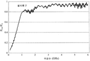
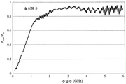
도 17은 0.1 내지 6 ㎓ 에서 기준예 1 의 근거리 전자기파 흡수 필름의 Ploss/Pin 을 도시하는 그래프이다.
도 18은 기준예 2 의 보어 가공된 복합 필름을 도시하는 현미경 사진이다.
도 19는 0.1 내지 6 ㎓ 에서 기준예 2 의 보어 가공된 복합 필름의 Ploss/Pin 을 도시하는 그래프이다.
도 20은 0.1 내지 6 ㎓ 에서 실시예 1 의 근거리 전자기파 흡수 필름의 S11, S21 및 Rtp 를 도시하는 그래프이다.
도 21은 0.1 내지 6 ㎓ 에서 실시예 1 의 근거리 전자기파 흡수 필름의 Ploss/Pin 을 도시하는 그래프이다.
도 22는 0.1 내지 6 ㎓ 에서 실시예 2 의 근거리 전자기파 흡수 필름의 S11, S21 및 Rtp 를 도시하는 그래프이다.
도 23은 0.1 내지 6 ㎓ 에서 실시예 2 의 근거리 전자기파 흡수 필름의 Ploss/Pin 을 도시하는 그래프이다.
도 24는 0.1 내지 6 ㎓ 에서 실시예 3 의 근거리 전자기파 흡수 필름의 S11, S21 및 Rtp 를 도시하는 그래프이다.
도 25는 0.1 내지 6 ㎓ 에서 실시예 3 의 근거리 전자기파 흡수 필름의 Ploss/Pin 을 도시하는 그래프이다.
도 26은 0.1 내지 6 ㎓ 에서 실시예 4 의 근거리 전자기파 흡수 필름의 S11, S21 및 Rtp 를 도시하는 그래프이다.
도 27은 0.1 내지 6 ㎓ 에서 실시예 4 의 근거리 전자기파 흡수 필름의 Ploss/Pin 을 도시하는 그래프이다.
도 28은 0.1 내지 6 ㎓ 에서 실시예 5 의 근거리 전자기파 흡수 필름의 S11, S21 및 Rtp 를 도시하는 그래프이다.
도 29는 0.1 내지 6 ㎓ 에서 실시예 5 의 근거리 전자기파 흡수 필름의 Ploss/Pin 을 도시하는 그래프이다. 1A is a partially enlarged plan view showing an embodiment of arrangements of fine laser beam bore-processed holes for forming a near-field electromagnetic wave absorbing film of the present invention.
1B is a cross-sectional view taken along line AA of FIG. 1A.
Fig. 1C is a partial enlarged view of Fig. 1A. Fig.
2 is a partially enlarged plan view showing another embodiment of arrangements of fine laser beam bore-processed holes for forming a near-field electromagnetic wave absorbing film of the present invention.
3 is a plan view showing an embodiment of arrangements of openings for forming the near-field electromagnetic wave absorbing film of the present invention.
4 is a plan view showing another embodiment of arrangements of openings for forming the near-field electromagnetic wave absorbing film of the present invention.
5 is a plan view showing another embodiment of arrangements of openings for forming the near-field electromagnetic wave absorbing film of the present invention.
6 is a plan view showing another embodiment of arrangements of openings for forming the near-field electromagnetic wave absorbing film of the present invention.
7 is a plan view showing another embodiment of arrangements of openings for forming the near-field electromagnetic wave absorbing film of the present invention.
8 is a plan view showing still another embodiment of arrangements of openings for forming the near-field electromagnetic wave absorbing film of the present invention.
Fig. 9 is a plan view showing another embodiment of arrangements of openings for forming the near-field electromagnetic wave absorbing film of the present invention.
10A is a perspective view showing an apparatus for measuring electrical resistance of a near-field electromagnetic wave absorbing film.
10B is a plan view showing the measurement of the electrical resistance of the near-field electromagnetic wave absorbing film by the apparatus of FIG. 10A.
Figure 10C is a cross-sectional view taken along line BB of Figure 10B.
11A is a plan view showing a system for evaluating the electromagnetic wave absorption ability of the near-field electromagnetic wave absorption film.
11B is a partial transverse front view showing a system for evaluating the electromagnetic wave absorption capability of the near-field electromagnetic wave absorbing film.
12 is a photomicrograph showing the bore-processed composite film of Reference Example 1. Fig.
13 is a photomicrograph showing the bore-processed composite film of Comparative Example 1. Fig.
14 is a micrograph showing the bore-processed composite film of Comparative Example 2. Fig.
15 is a graph showing the relationships between the frequencies of incident electromagnetic waves of the bore-processed composite films of Reference Example 1 and Comparative Examples 1 and 2 and S 11 .
16 is a graph showing the relationship between the frequency of the incident electromagnetic waves of the bore-processed composite films of Reference Example 1 and Comparative Examples 1 and 2 and the transmission attenuation power ratio (Rtp).
17 is a graph showing the P loss / P in of the near-field electromagnetic wave-absorbing film of Reference Example 1 at 0.1 to 6 GHz.
18 is a micrograph showing the bore-processed composite film of Reference Example 2. Fig.
19 is a graph showing P loss / P in of the bore-processed composite film of Reference Example 2 at 0.1 to 6 GHz.
20 is a graph showing S 11 , S 21 and Rtp of the near-field electromagnetic wave absorbing film of Example 1 at 0.1 to 6 GHz.
21 is a graph showing P loss / P in of the near field electromagnetic wave absorbing film of Example 1 at 0.1 to 6 GHz.
22 is a graph showing S 11 , S 21 and Rtp of the near-field electromagnetic wave-absorbing film of Example 2 at 0.1 to 6 GHz.
23 is a graph showing P loss / P in of the near-field electromagnetic wave-absorbing film of Example 2 at 0.1 to 6 GHz.
24 is a graph showing S 11 , S 21 and Rtp of the near-field electromagnetic wave absorbing film of Example 3 at 0.1 to 6 GHz.
25 is a graph showing P loss / P in of the near field electromagnetic wave absorbing film of Example 3 at 0.1 to 6 GHz.
26 is a graph showing S 11 , S 21 and Rtp of the near field electromagnetic wave absorbing film of Example 4 at 0.1 to 6 GHz.
27 is a graph showing the P loss / P in of the near field electromagnetic wave absorbing film of Example 4 at 0.1 to 6 GHz.
28 is a graph showing S 11 , S 21 and Rtp of the near-field electromagnetic wave-absorbing film of Example 5 at 0.1 to 6 GHz.
29 is a graph showing P loss / P in of the near field electromagnetic wave absorbing film of Example 5 at 0.1 to 6 GHz.
본 발명의 실시예들은 첨부된 도면들을 참조하여 설명될 것이며, 일 실시예에 관한 설명은 달리 언급되지 않는다면 다른 실시예들에도 적용 가능한 것에 주의해야 한다. 또한, 이후의 설명은 제한적인 것이 아니며, 오히려 다양한 수정들이 본 발명의 범주 내에서 이루어질 수 있다. It should be noted that the embodiments of the present invention will be described with reference to the accompanying drawings, and explanations of one embodiment are applicable to other embodiments unless otherwise mentioned. Furthermore, the following description is not meant to be limiting, but various modifications may be made within the scope of the present invention.
[1] 보어 가공된 얇은 금속 필름[1] bore-processed thin metal film
도 1a 내지 도 1c는 본 발명의 근거리 전자기파 흡수 필름을 형성하기 위한 미세한 레이저 빔 보어 가공된 홀들의 배열들의 실시예를 도시한다. 많은 수의 미세한 레이저 빔 보어 가공된 홀들이 제공되는 얇은 금속 필름은 이후에 "보어 가공된 얇은 금속 필름" 으로 지칭된다. 이러한 보어 가공된 얇은 금속 필름(1)은 플라스틱 필름(10)의 표면에 형성되는 단일 층 또는 다중 층의 얇은 금속 필름(11)에 레이저 빔들에 의해 2 개의 교차하는 라인들에 홀(12)들을 형성함으로써 얻어진다. Figs. 1A to 1C illustrate an embodiment of arrangements of fine laser beam bore-processed holes for forming a near-field electromagnetic wave absorbing film of the present invention. The thin metal film provided with a large number of fine laser beam bore machined holes is hereinafter referred to as "bore machined thin metal film ". The bore-processed
(1) 플라스틱 필름(1) Plastic films
플라스틱 필름(10)을 형성하는 수지들은 이들이 절연성 외에 충분한 강도, 가변성 및 작업성을 갖는 한 특별히 제한적이지 않고, 이들은, 예컨대 폴리에스테르(폴리에틸렌 테레프탈레이트 등), 폴리아릴렌 설파이드(폴리페닐렌 설파이드 등), 폴리아미드, 폴리이미드, 폴리아미드이미드, 폴리에테르 설폰, 폴리에테르에테르케톤, 폴리카보네이트, 아크릴 수지, 폴리스티렌, 폴리올레핀(폴리에틸렌, 폴리프로필렌 등) 등일 수 있다. 강도 및 비용의 측면에서, 폴리에틸렌 테레프탈레이트(PET)가 바람직하다. 플라스틱 필름(10)의 두께는 약 10 내지 100 ㎛ 일 수 있다.The resins forming the
(2) 얇은 금속 필름(2) Thin metal film
얇은 금속 필름(11)을 형성하는 금속들은 이들이 전도성을 갖는 한 특별히 제한적이지 않고, 내부식성 및 비용의 양태로부터, 이들은 바람직하게는 알루미늄, 구리, 은, 주석, 니켈, 코발트, 크롬 및 이들의 합금들, 특히 알루미늄, 구리, 니켈 및 이들의 합금들이다. 얇은 금속 필름의 두께는 바람직하게는 10 내지 300 ㎚, 더 바람직하게는 20 내지 200 ㎚, 가장 바람직하게는 30 내지 150 ㎚ 이다. 얇은 금속 필름(11)은 증기 증착(진공 증기 증착, 스퍼터링(sputtering) 또는 이온 도금과 같은 물리적 증기 증착, 또는 플라즈마 CVD, 열 CVD 또는 광 CVD 와 같은 화학적 증기 증착), 도금 또는 포일 본딩(foil bonding)에 의해 형성될 수 있다. The metals forming the
얇은 금속 필름(11)이 단일 층일 때, 얇은 금속 필름(11)은 전도성, 내부식성 및 비용의 양태로부터 바람직하게는 알루미늄 또는 니켈로 만들어진다. 얇은 금속 필름(11)이 복합 층일 때, 하나의 층은 비자기 금속으로 형성될 수 있고, 다른 층은 자기 금속에 의해 형성될 수 있다. 비자기 금속은 알루미늄, 구리, 은, 주석 또는 이들의 합금들일 수 있고, 자기 금속은 니켈, 코발트, 크롬 또는 이들의 합금들일 수 있다. 비자기 금속 층의 두께 및 자기 금속 층의 두께는 이들의 총 두께가 상기 범위 내에 있는 한 제한적이지 않다. When the
(3) 레이저 빔 보어 가공된 홀들(3) laser beam bore machined holes
도 1a 내지 도 1c에 도시된 바와 같이, 각각의 레이저 빔 보어 가공된 홀(12)은 플라스틱 필름(10)의 개방 없이, 얇은 금속 필름(11)에 대한 레이저 빔의 조사(irradiation)에 의해 금속을 소멸시킴으로써(evaporating) 형성되는 실질적으로 원형 홀이다. 각각의 레이저 빔 보어 가공된 홀(12)의 직경(D)은 200 ㎛ 이하이다. 직경(D)이 200 ㎛ 초과일 때, 단위 면적에 형성되는 레이저 빔 보어 가공된 홀(12)들의 수는 너무 적고, 레이저 빔 보어 가공된 홀(12)들 사이에 남아있는 얇은 금속 필름(11)의 너무 큰 부분들을 초래하며, 이는 반사 필름의 역할을 하고, 따라서 충분한 전자기파 흡수 능력을 얻는 것에 실패한다. 각각의 레이저 빔 보어 가공된 홀(12)의 직경(D)은 바람직하게는 100 ㎛ 이하, 더 바람직하게는 20 내지 100 ㎛ 이다. As shown in Figs. 1A to 1C, each laser beam bore-machined
묘사된 실시예에서, 레이저 빔 보어 가공된 홀(12)들은 얇은 금속 필름(11)의 2 개의 교차하는 라인들에 배열된다. 얇은 금속 필름(11)은 레이저 빔 보어 가공된 홀들의 교차하는 라인(12a, 12b)들에 의해 개별적인 주요 나머지 부분(13)들로 구획된다. 레이저 빔 보어 가공된 홀(12)들이 적어도 부분적인 간격들을 갖고 배열되기 때문에, 얇은 금속 필름(11)의 간격 부분들은 좁은 브리지형(bridge-like) 부분(14)들로서 남아있는다. 따라서, "남아있는 얇은 금속 필름 부분들" 이라고 불리는, 레이저 빔 보어 가공된 홀(12)들을 형성한 후에 남아있는 얇은 금속 필름 부분(11a)들은 주요 나머지 부분(13)들 그리고 좁은 브리지형 부분(14)들로 이루어진다.In the depicted embodiment, the laser beam bore machined
레이저 빔 보어 가공된 홀(12)들은 바람직하게는 양쪽의 라인(12a, 12b)들에 간격들을 갖고 배열된다. 인접한 레이저 빔 보어 가공된 홀(12)들의 간격(W)들(브리지형 부분(14)들의 폭들)은 50 ㎛ 이하이다. 간격(W)들이 50 ㎛ 초과일 때, 보어 가공된 얇은 금속 필름(1)은 바람직한 전기 저항을 갖지 않는다. 인접한 레이저 빔 보어 가공된 홀(12)들의 간격(W)들(브리지형 부분(14)들의 폭들)은 바람직하게는 20 ㎛ 이하, 더 바람직하게는 1 내지 15 ㎛ 이다. 따라서, 브리지형 부분(14)들의 최대 폭(Wmax)은 50 ㎛, 바람직하게는 20 ㎛ 이다. 브리지형 부분(14)들의 평균 폭(Wav)은 3 내지 30 ㎛, 바람직하게는 5 내지 20 ㎛ 이다. The laser beam
레이저 빔 스폿들 자체가 원형이지만, 레이저 빔들에 의해 소멸되는 얇은 금속 필름(1)의 영역들은 완전한 원형이 아니며, 인접한 레이저 빔 보어 가공된 홀(12)들 사이의 간섭으로 인해 오히려 약간 불규칙한 외형들을 가지려는 경향이 있다. 예컨대, 인접한 레이저 빔 보어 가공된 홀(12)들 사이에 공간이 없을 때, 양쪽의 레이저 빔 보어 가공된 홀(12)들은 접촉하지 않지만, 작은 폭들을 갖는 브리지형 부분(14)들을 가질 수 있다. 이는 소멸된 금속이 인접한 레이저 빔 스폿들 사이에서 고형화되고, 좁은 브리지형 부분(14)들을 초래한다는 사실로 인한 것으로 보인다. 따라서, 동일한 간격으로 배열된 레이저 빔 스폿들에 의해서라도, 얇은 금속 필름(11)의 소멸에 의해 사실상 형성되는 레이저 빔 보어 가공된 홀(12)들은 동일한 간격을 갖지 않으며, 브리지형 부분(14)들은 50 ㎛ 이하의 범위 내의 상이한 폭(W)들을 갖는다. 따라서, 본 발명의 근거리 전자기파 흡수 필름은 넓은 범위의 주파수에서 우수한 전자기파 흡수 능력을 갖는다. Although the laser beam spots themselves are circular, the areas of the
레이저 빔 보어 가공된 홀들의 라인(12a, 12b)들은 45 내지 90°의 각도(θ)로 교차하고, 이에 의해 낮은 비등방성을 갖는 높은 전자기파 흡수 능력을 제공한다. 교차 각도(θ)가 45° 미만일 때, 충분한 전자기파 흡수 능력이 얻어질 수 없다. 90°의 교차 각도(θ)는 최대 전자기파 흡수 능력을 제공한다. 바람직한 교차 각도(θ)는 60 내지 90°이다. The lines of laser beam
주요 나머지 부분(13)들의 크기는 주로 인접한 레이저 빔 보어 가공된 홀들의 라인(12a, 12b)들 사이의 중심선 거리(T)에 의존한다. 주요 나머지 부분(13)들의 크기가 근거리 전자기파 흡수 필름(20)의 전기 저항(따라서, 전자기파 흡수 능력)에 영향을 미치기 때문에, 레이저 빔 보어 가공된 홀들의 인접한 라인(12a, 12b)들 사이의 중심선 거리(T)는 바람직한 전기 저항을 갖도록 설정되어야 한다. 구체적으로, 레이저 빔 보어 가공된 홀들의 인접한 라인(12a, 12b)들 사이의 중심선 거리(T)는 바람직하게는 100 내지 400 ㎛, 더 바람직하게는 150 내지 300 ㎛ 이다. The size of the major remaining
도 2는 본 발명의 근거리 전자기파 흡수 필름을 형성하기 위한 미세한 레이저 빔 보어 가공된 홀들의 배열들의 다른 실시예를 도시한다. 이러한 보어 가공된 얇은 금속 필름(1')에서, 복수의 레이저 빔 보어 가공된 홀(12)들이 양쪽 수직 방향들로 실질적으로 동일한 간격(W)을 갖고 배열된다. 상기 실시예에서와 같이, 간격(W)은 50 ㎛ 이하, 바람직하게는 20 ㎛ 이하, 더 바람직하게는 1 내지 15 ㎛ 이다. Figure 2 shows another embodiment of arrangements of fine laser beam bore machined holes for forming a near field electromagnetic wave absorbing film of the present invention. In this bore-processed thin metal film 1 ', a plurality of laser beam bore-processed
(4) 개구들(4)
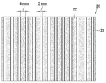
투과 가시성을 주는 크기의 복수의 개구들은, 근거리 전자기파 흡수 필름을 제조하기 위해, 보어 가공된 얇은 금속 필름에 부분적으로 형성된다. 개구들의 형상들 및 배열들은, 충분한 전자기파 흡수 능력을 확보하면서 필요한 투과 가시성이 얻어지는 한 제한적이지 않다. 개구들의 크기들은, 충분한 전자기파 흡수 능력을 확보하면서 필요한 투과 가시성이 얻어지는 한 제한적이지 않지만, 예컨대, 이들이 도 2에 도시된 바와 같이 원형일 때, 이들은 바람직하게는 수 밀리미터 내지 수십 밀리미터의 직경들을 갖는다. 일반적으로, 개구들은 바람직하게는 직경 또는 폭이 2 내지 20 ㎜ 정도 크기이다. 도 3 내지 도 9는 개구들의 형상들, 크기들 및 배열들의 실시예들을 도시한다. 개구들이 하나의 방향으로 배열될 수 있지만, 이들은 바람직하게는 적어도 2 개의 방향들로 배열된다. A plurality of apertures of a size giving transmission visibility are partially formed in the bore-processed thin metal film to produce a near-field electromagnetic wave absorbing film. The shapes and arrangements of the openings are not limited as long as necessary transparency visibility is obtained while ensuring sufficient electromagnetic wave absorption capability. The sizes of the openings are not limited as long as the required transmission visibility is obtained while ensuring sufficient electromagnetic wave absorption capability, but when they are circular, for example, as shown in Fig. 2, they preferably have diameters of several millimeters to several tens of millimeters. Generally, the openings are preferably about 2 to 20 mm in diameter or width. Figures 3-9 illustrate embodiments of shapes, sizes, and arrangements of openings. Although the openings can be arranged in one direction, they are preferably arranged in at least two directions.
도 3에 도시된 근거리 전자기파 흡수 필름(20)에서, 복수의 평행한 슬릿형(slit-like) 개구(21)들이 보어 가공된 얇은 금속 필름(1)에 형성된다. 개구 후(post-opening) 남아있는 부분들이라고 불릴 수 있는, 슬릿형 개구(21)들 형성 후에 남아있는 얇은 금속 필름 부분(22)들은 리본(ribbon) 형상이다. In the near-field electromagnetic
도 4에 도시된 근거리 전자기파 흡수 필름(20)에서, 복수의 사각형 개구(21)들이 보어 가공된 얇은 금속 필름(1)에 평행하게 길이방향으로 그리고 횡방향으로 형성된다. 개구 후 남아있는 부분들이라고 불릴 수 있는, 사각형 개구(21)들 형성 후에 남아있는 얇은 금속 필름 부분(22)들은 격자(lattice) 형상이다. In the near-field electromagnetic
도 5에 도시된 근거리 전자기파 흡수 필름(20)에서, 복수의 정사각형 개구(21)들이 보어 가공된 얇은 금속 필름(1)에 평행하게 길이방향으로 그리고 횡방향으로 형성된다. 개구 후 남아있는 부분들이라고 불릴 수 있는, 정사각형 개구(21)들 형성 후에 남아있는 얇은 금속 필름 부분(22)들은 격자 형상이다. In the near-field electromagnetic
도 6에 도시된 근거리 전자기파 흡수 필름(20)에서, 복수의 원형 개구(21)들이 보어 가공된 얇은 금속 필름(1)에 평행하게 길이방향으로 그리고 횡방향으로 형성된다. 개구 후 남아있는 부분들이라고 불릴 수 있는, 원형 개구(21)들 형성 후에 남아있는 얇은 금속 필름 부분(22)들은 격자 형상이다. In the near-field electromagnetic
도 7에 도시된 근거리 전자기파 흡수 필름(20)에서, 복수의 삼각형 개구(21)들이 보어 가공된 얇은 금속 필름(1)에 평행하게 길이방향으로 그리고 횡방향으로 형성된다. 개구 후 남아있는 부분들이라고 불릴 수 있는, 삼각형 개구(21)들 형성 후에 남아있는 얇은 금속 필름 부분(22)들은 변형된 격자 형상이다. In the near-field electromagnetic
도 8에 도시된 근거리 전자기파 흡수 필름(20)에서, 복수의 마름모(rhombic) 개구(21)들이 보어 가공된 얇은 금속 필름(1)에 평행하게 길이방향으로 그리고 횡방향으로 형성된다. 개구 후 남아있는 부분들이라고 불릴 수 있는, 마름모(기울어진 정사각형) 개구(21)들 형성 후에 남아있는 얇은 금속 필름 부분(22)들은 변형된 격자 형상이다.In the near-field electromagnetic
도 9에 도시된 근거리 전자기파 흡수 필름(20)에서, 복수의 쌍들의 삼각형 개구(21)들이 보어 가공된 얇은 금속 필름(1)에 평행하게 길이방향으로 그리고 횡방향으로 형성된다. 개구 후 남아있는 부분들이라고 불릴 수 있는, 삼각형 개구(21)들 형성 후에 남아있는 얇은 금속 필름 부분(22)들은 변형된 격자 형상이다.In the near-field electromagnetic
도 3 내지 도 9에 도시된 바와 같이, 개구 후 남아있는 부분(22)들은 적어도 하나의 방향으로, 바람직하게는 적어도 2 개의 방향들로 연결되어야 한다. 보어 가공된 얇은 금속 필름(1)에 대한 개구(21)들의 면적비([100 x 개구(21)들의 총 면적/(개구(21)들의 총 면적 + 개구 후 남아있는 부분(22)들의 총 면적)]는 바람직하게는 15 내지 60 %, 더 바람직하게는 20 내지 50 % 이다. 개구(21)들의 면적비가 15 % 미만일 때, 충분한 투과 가시성이 얻어질 수 없다. 다른 한편, 개구(21)들의 면적비가 60 % 초과일 때, 충분한 전자기파 흡수 능력이 확보될 수 없다.As shown in Figures 3-9, the remaining
(5) 전기 저항(5) Electrical resistance
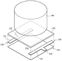
근거리 전자기파 흡수 필름(20)의 전자기파 흡수 능력은 기본적으로 보어 가공된 얇은 금속 필름(1)의 전자기파 흡수 능력에 의존한다. 집중적인 연구는 보어 가공된 얇은 금속 필름(1)의 전자기파 흡수 능력이 레이저 빔 보어 가공된 홀(12)들 형성 후에 남아있는 보어 가공된 얇은 금속 필름 부분(11a)들(남아있는 보어 가공된 얇은 금속 필름 부분(11a)들 = 보어 가공된 주요 나머지 부분(13)들 + 보어 가공된 브리지형 부분(14)들)의 크기들 및 전기 저항에 의존한다는 것을 밝혀냈다. 50 내지 300 Ω/㎠ 의 전기 저항을 갖는 보어 가공된 얇은 금속 필름(1)은 넓은 범위의 주파수에서 우수한 전자기파 흡수 능력을 갖는다.The electromagnetic wave absorbing capability of the near-field electromagnetic
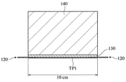
보어 가공된 얇은 금속 필름(1)의 전기 저항은, 도 10a 내지 도 10c 에 도시된 기기를 사용하여, 압력 하에서 DC 2-단자 방법(간단하게 "압력 하 2-단자 방법" 이라고 불림)에 의해, 플라스틱 필름(10)의 표면에 보어 가공된 얇은 금속 필름(1)을 포함하는 복합 필름의 시편(TP1)에 대해 측정된다. 구체적으로, 10 ㎝ x 10 ㎝ 의 정사각형 시편(TP1)이 편평하고 경질의 절연 표면 위에 그의 보어 가공된 얇은 금속 필름(1)이 있도록 놓이고, 길이가 10 ㎝, 폭이 1 ㎝ 그리고 두께가 0.5 ㎜ 인 전극 본체 부분(121), 그리고 전극 본체 부분(121)의 중심 측으로부터 연장하는 폭 1㎝ 그리고 두께가 0.5 ㎜ 인 전극 연장부(122)를 각각 포함하는 한 쌍의 전극(120, 120)들이 정사각형 시편(TP1)의 대향 측 부분들에 부착된다. 10 ㎝ x 10 ㎝ x 5 ㎜ 의 투명 아크릴 플레이트(130)가 시편(TP1)과 양쪽 전극(120, 120)들에, 이들을 완전히 커버하도록 놓이고, 직경이 10 ㎝ 인 원통형 추(140)(3.85 ㎏)가, 전기 저항을 판정하기 위해 양쪽 전극 연장부(222, 222)들 사이에서 유동하는 전류를 측정하기 위해, 투명 아크릴 플레이트(130)에 놓인다. 상기 조건들 하에서 측정된 전기 저항은 "Ω/100 ㎠" 에 의해 표현된다. The electrical resistance of the bore-processed
보어 가공된 얇은 금속 필름(1)(근거리 전자기파 흡수 필름(20))은 50 내지 300 Ω/100 ㎠ 범위의 전기 저항을 가져야 한다. 전기 저항이 50 Ω/100 ㎠ 미만이거나 300 Ω/100 ㎠ 초과일 때, 근거리 전자기파 흡수 필름(20)은 충분한 전자기파 흡수 능력을 갖지 않는다. 근거리 전자기파 흡수 필름(20)의 전기 저항은 바람직하게는 60 내지 250 Ω/100 ㎠, 더 바람직하게는 80 내지 200 Ω/100 ㎠ 이다.The bore-processed thin metal film 1 (near-electromagnetic wave absorbing film 20) should have an electric resistance in the range of 50 to 300? / 100 cm2. When the electric resistance is less than 50 Ω / 100
(6) 보호층 (6) Protective layer
보어 가공된 얇은 금속 필름(1)을 보호하기 위해, 보호 플라스틱 층(도시되지 않음)이 바람직하게는 그 위에 형성된다. 보호 플라스틱 층을 위한 플라스틱 필름은 플라스틱 필름(10)과 동일할 수 있다. 보호 플라스틱 층의 두께는 약 10 내지 100 ㎛ 이다. 분리를 방지하기 위해, 플라스틱 필름은 바람직하게는 보호층으로서 근거리 전자기파 흡수 필름(20)에 열 적층된다(heat-laminated). 보호 플라스틱 층이 PET 필름에 의해 형성될 때, 열 적층 온도는 110 내지 150 ℃ 일 수 있다. In order to protect the bored
보호층을 위한 플라스틱 필름이 보통 레이저 빔 보어 가공된 홀들 및 개구들이 플라스틱 필름(10) 상의 얇은 금속 필름(11)에 형성된 후에 근거리 전자기파 흡수 필름(20)에 부착되지만, 레이저 빔 보어 가공된 홀들 및 개구들은, 보호 플라스틱 필름에 미리 많은 미세한 구멍들이 제공되는 한, 보호 플라스틱 필름이 얇은 금속 필름(11)에 부착된 후에 형성될 수 있다. 보호 플라스틱 필름의 미세한 구멍들의 형성은 일본 특허 2063411 에 설명된 방법에 의해 실시될 수 있다. Although the plastic film for the protective layer is usually attached to the near-field electromagnetic
[2] 근거리 전자기파 흡수 필름의 전자기파 흡수 능력[2] Electromagnetic wave absorption ability of a near-field electromagnetic wave absorbing film
(1) 투과 감쇠 파워 비(1) Transmission damping power ratio
도 11a 및 도 11b에 도시된 바와 같이 50-Ω 마이크로스트립라인(microstripline; MSL)(64.4 ㎜ x 4.4 ㎜), 마이크로스트립라인(MSL)을 지지하는 절연 기재(220), 절연 기재(220)의 하부 표면에 부착되는 접지된(grounded) 전극(221), 마이크로스트립라인(MSL)의 양단부들에 연결되는 전도성 핀(222, 222)들, 네트워크 분석기(NA) 및 네트워크 분석기(NA)를 전도성 핀(222, 222)들에 연결하는 동축 케이블(223, 223)들을 포함하는 시스템을 사용하여, 각각의 근거리 전자기파 흡수 필름(20)의 시편(TP2)이 0.1 내지 6 ㎓ 의 입력 전자기파에 대한 그의 반사된 파장의 파워(S11) 및 투과된 파장의 파워(S21)를 측정하기 위해 마이크로스트립라인(MSL)에 부착되며, 이에 의해 이하의 공식(1)에 의해 그의 투과 감쇠 파워 비(Rtp)를 판정한다 :As shown in Figs. 11A and 11B, a 50-Ω microstripline (MSL) (64.4 mm x 4.4 mm), an insulating
Rtp = -10 x log [10S21 /10/(1-10S11 /10)] … (1). Rtp = -10 x log [10 S21 / 10 / (1-10 S11 / 10 )] ... (One).
(2) 노이즈 흡수 비(2) Noise absorption ratio
도 11a 및 도 11b에 도시된 시스템에서, 입력된 파워(Pin) = 반사된 파장의 파워(S11) + 투과된 파장의 파워(S21) + 흡수된 파워(파워 손실)(Ploss) 이다. 따라서, 소읍 흡수 비(Ploss/Pin)는 입력된 파워(Pin)로부터 반사된 파장의 파워(S11) 및 투과된 파장의 파워(S21)를 빼고, 결과인 파워 손실(Ploss)을 입력된 파워(Pin)로 나눔으로써 판정된다.In the system shown in Figs. 11A and 11B, the input power P in = the power of reflected light S 11 + the power of transmitted light S 21 + the absorbed power P loss , to be. Therefore, the absorption factor (P loss / P in ) of the far field is obtained by subtracting the power S 11 of the reflected wave and the power S 21 of the transmitted wave from the input power P in , and the resulting power loss P loss ) Is divided by the input power (P in ).
[3] 근거리 전자기파 흡수 필름의 제조 방법[3] Manufacturing method of a near-field electromagnetic wave absorbing film
직경이 200 ㎛ 이하인 레이저 빔 보어 가공된 홀(12)들은 먼저, 예컨대 증기 증착에 의해, 플라스틱 필름(10)에 형성된 얇은 금속 필름(11)의 표면 전체에 50 ㎛ 이하의 간격들로 형성된다. 보어 가공된 얇은 금속 필름(1)은 그 후 투과 가시성을 주는 크기의 복수의 개구(21)들이 부분적으로 제공된다. 개구(21)들은 레이저 빔들을 조사함으로써 형성될 수 있다. 이러한 경우, 레이저 빔 보어 가공된 홀(12)들 및 개구(21)들은 레이저 빔들의 한 번의 조사 작업에 의해 형성될 수 있지만, 2 단계들에 의한 레이저 빔 보어 가공된 홀(12)들 및 개구(21)들의 별개의 형성은 더 높은 효율로 근거리 전자기파 흡수 필름(20)을 제조할 수 있다. 부차적으로, 개구(21)들은 포토리소그래피(photolithography)에 의해 형성될 수 있다. The laser beam bore-processed
본 발명은 제한의 의도 없이 이하의 실시예들을 참조하여 더 상세하게 설명될 것이다.The present invention will be described in more detail with reference to the following embodiments without any intention of limitation.
기준예 1, 및 비교예 1 및 2Reference Example 1, and Comparative Examples 1 and 2
16 ㎛ 만큼 두꺼운 각각의 PET 필름(10)에 진공 증기 증착된, 50 ㎚ 만큼 두꺼운 얇은 Ni 필름(11)에, 도 12 내지 도 14에 도시된 보어 가공된 얇은 Ni 필름(1)을 갖는 복합 필름을 제조하기 위해, 3-축 하이브리드 레이저 마커(Keyence Corporation 으로부터 이용 가능한 MD-X1000)에 의해 2 개의 교차하는 라인들에 직경 60 ㎛ 의 레이저 빔 보어 가공된 홀(12)들이 제공되었다. 각각의 복합 필름에서 절단된 정사각형 시편(TP1)(10 ㎝ x 10 ㎝)의 전기 저항은 섹션 [1] (5) 에 설명된 방법에 의해 측정되었다. 결과들은 표 1에 도시된다.A composite film having a bore-processed thin Ni film (1) shown in Figs. 12 to 14 was attached to a thin Ni film (11) thicker by 50 nm vacuum-vapor-deposited on each PET film (10) Laser beam bore machined
주의 : (1) 레이저 빔 보어 가공된 홀들의 2 개의 라인들의 교차 각도(θ) Note: (1) the angle of intersection (θ) of the two lines of laser beam bored holes,
(2) 브리지형 부분들의 폭(W) (2) The width (W) of the bridge-
각각의 복합 필름으로부터 절단된 시편(TP2)(55.2 ㎝ x 4.7 ㎜)은, 섹션 [2], (1) 및 (2) 에 설명된 방법에 의해 0.1 내지 6 ㎓ 의 주파수 범위의 입력 파워(Pin)에 대한 반사된 파장의 파워(S11) 및 투과된 파장의 파워(S21)를 측정하기 위해, 도 11a 및 도 11b에 도시된 시스템의 마이크로스트립라인(MSL)에 부착되었고, 이에 의해 0.1 내지 6 ㎓ 의 주파수 범위의 투과 감쇠 파워 비(Rtp) 및 노이즈 흡수 비(Ploss/Pin)를 판정한다. 0.1 내지 6 ㎓ 의 주파수 범위의 S11, 투과 감쇠 파워 비(Rtp) 및 노이즈 흡수 비(Ploss/Pin)는 도 15, 도 16 및 도 17에 각각 도시된다. 도 15로부터 명백한 바와 같이, 너무 적은 레이저 빔 보어 가공된 홀(12)들(너무 낮은 전기 저항)을 갖는 비교예 1 에서 큰 반사된 파장 파워(S11)가 있었다. 또한, 도 16으로부터 명백한 바와 같이, 과도한 레이저 빔 보어 가공된 홀(12)들(너무 높은 전기 저항)을 갖는 비교예 2 에서 낮은 투과 감쇠 파워 비(Rtp)가 있었다. 또한, 도 17로부터 명백한 바와 같이, 기준예 1 의 복합 필름은 우수한 노이즈 흡수 비(Ploss/Pin)를 가졌다.The specimen TP2 (55.2 cm x 4.7 mm) cut from the respective composite films was subjected to a measurement of the input power P (P) of 0.1 to 6 GHz by the method described in sections [2], (1) (MSL) of the system shown in Figs. 11A and 11B to measure the power (S 11 ) of the reflected wavelength and the power (S 21 ) of the transmitted wavelength with respect to the in- The transmission attenuation power ratio (Rtp) and the noise absorption ratio (P loss / P in ) in the frequency range of 0.1 to 6 GHz are determined. S 11 , the transmission attenuation power ratio (Rtp) and the noise absorption ratio (P loss / P in ) in the frequency range of 0.1 to 6 GHz are shown in Figs. 15, 16 and 17, respectively. As is apparent from Fig. 15, there was a large reflected wavelength power S 11 in Comparative Example 1 having too few laser beam bore machined holes 12 (too low electrical resistance). 16, there was a low transmission attenuation power ratio Rtp in Comparative Example 2 having excessive laser beam bore machined holes 12 (too high electrical resistance). Further, as apparent from Fig. 17, the composite film of Reference Example 1 had an excellent noise absorption ratio (P loss / P in ).
기준예 2Reference Example 2
16 ㎛ 만큼 두꺼운 각각의 PET 필름(10)에 진공 증기 증착된, 80 ㎚ 만큼 두꺼운 얇은 Al 필름(11)에, 도 18에 도시된 보어 가공된 얇은 Al 필름(1)을 갖는 복합 필름을 제조하기 위해, 3-축 하이브리드 레이저 마커(Keyence Corporation 으로부터 이용 가능한 MD-X1000)에 의해 2 개의 교차하는 라인들에 직경 80 ㎛ 의 레이저 빔 보어 가공된 홀(12)들이 제공되었다. 레이저 빔 보어 가공된 홀(12)들의 간격(W)들은 약 20 ㎛ 였다. 기준예 1 에서와 동일한 방법에 의해 측정된 각각의 복합 필름의 전기 저항은 60 내지 80 Ω/100 ㎠ 였다. A composite film having the bore-processed
0.1 내지 6 ㎓ 의 주파수 범위의 복합 필름의 반사된 파장의 파워(S11) 및 투과된 파장의 파워(S21)가, 노이즈 흡수 비(Ploss/Pin)를 판정하기 위해, 기준예 1 에서와 동일한 방식으로 측정되었다. 0.1 내지 6 ㎓ 의 주파수 범위의 노이즈 흡수 비(Ploss/Pin)가 도 19에 도시된다. 도 19로부터 명백한 바와 같이, 레이저 빔 보어 가공된 홀(12)들 및 전기 저항이 본 발명의 요건들을 충족하는, 기준예 2 의 복합 필름은 높은 노이즈 흡수 비(Ploss/Pin)를 가졌다. The power (S 11 ) of the reflected wavelength and the power (S 21 ) of the transmitted wavelength of the composite film in the frequency range of 0.1 to 6 GHz were measured in the same manner as in Reference Example 1 (1) to determine the noise absorption ratio (P loss / P in ) Was measured in the same manner as in FIG. The noise absorption ratio (P loss / P in ) in the frequency range of 0.1 to 6 GHz is shown in Fig. As is apparent from Fig. 19, the composite film of Reference Example 2, in which laser beam bore-processed
실시예 1 내지 5Examples 1 to 5
이하의 표 2에 도시된 바와 같이, 도 3 내지 도 6 그리고 도 9 중 임의의 하나에 도시된 개구(21)들은, 근거리 전자기파 흡수 필름을 제조하기 위해 기준예 1 및 2의 각각의 복합 필름에 형성되었다. 0.1 내지 6 ㎓ 의 주파수 범위의 입력 파워(Pin)에 대한 각각의 근거리 전자기파 흡수 필름의 시편(TP2)의 반사된 파장의 파워(S11) 및 투과된 파장의 파워(S21)는, 0.1 내지 6 ㎓ 의 주파수 범위의 투과 감쇠 파워 비(Rtp) 및 노이즈 흡수 비(Ploss/Pin)를 판정하기 위해 기준예 1 에서와 동일한 방식으로 측정되었다. 실시예 1 내지 5를 참조하면, 도 20, 도 22, 도 24, 도 26 및 도 28은 0.1 내지 6 ㎓ 의 주파수 범위의 S11, S21 및 Rtp 를 도시하고, 도 21, 도 23, 도 25, 도 27 및 도 29는 0.1 내지 6 ㎓ 의 주파수 범위의 Ploss/Pin 을 도시한다. As shown in the following Table 2, the
금속(두께 : ㎚)Thin metal film
Metal (thickness: nm)
Ni(50)Reference Example 1
Ni (50)
Al(80)Reference Example 2
Al (80)
Al(80)Reference Example 2
Al (80)
Al(80)Reference Example 2
Al (80)
Al(80)Reference Example 2
Al (80)
도 20 내지 도 29로부터 명백한 바와 같이, 실시예 1 내지 5 의 임의의 근거리 전자기파 흡수 필름들은 작은 반사된 파장의 파워(S11), 그리고 높은 투과 감쇠 파워 비(Rtp)들 및 노이즈 흡수 비(Ploss/Pin)들을 가졌다. 또한, 실시예 1 내지 5 의 근거리 전자기파 흡수 필름들은, 양호한 투과 가시성을 제공하는, 15 내지 60 % 의 개구 면적비들을 가졌다. As apparent from Figs. 20 to 29, any of the short-range electromagnetic wave absorbing films of Examples 1 to 5 has a small reflected wavelength power S 11 and a high transmission attenuation power ratio Rtp and a noise absorption ratio P loss / P in ). In addition, the near-field electromagnetic wave absorbing films of Examples 1 to 5 had aperture area ratios of 15 to 60%, which provided good transmission visibility.
1 : 보어 가공된 얇은 금속 필름
10 : 플라스틱 필름
11 : 얇은 금속 필름
11a : 남아있는 얇은 금속 필름 부분
12 : 레이저 빔 보어 가공된 홀
12a, 12b : 레이저 빔 보어 가공된 홀들의 라인
13 : 주요 나머지 부분
14 : 브리지형 부분
20 : 근거리 전자기파 흡수 필름
21 : 개구
22 : 개구 후 남아있는 부분
120 : 전극
121 : 전극 본체 부분
122 : 전극 연장부
130 : 투명 아크릴 플레이트
140 : 원통형 추
220 : 절연 기재
221 : 접지된 전극
222 : 전도성 핀
223 : 동축 케이블
D : 레이저 빔 보어 가공된 홀의 직경
W : 브리지형 부분의 폭
T : 인접한 레이저 빔 보어 가공된 홀들의 라인들 사이의 중심선 거리
TP1, TP2 : 근거리 전자기파 흡수 필름의 시편
MSL : 마이크로스트립라인
NA : 네트워크 분석기1: Thin metal film processed by bore
10: Plastic film
11: Thin metal film
11a: Remaining thin metal film portion
12: laser beam bore machined hole
12a, 12b: lines of laser beam bore machined holes
13: Major rest
14: Bridge type portion
20: Near-field electromagnetic wave absorption film
21: opening
22: Portion remaining after opening
120: Electrode
121: Electrode body portion
122: electrode extension part
130: Clear acrylic plate
140: Cylindrical weight
220: Insulation board
221: grounded electrode
222: Conductive pin
223: Coaxial cable
D: Diameter of laser beam bore machined hole
W: Width of the bridge portion
T: Centerline distance between lines of adjacent laser beam bore machined holes
TP1, TP2: Specimen of short-range electromagnetic wave absorption film
MSL: Microstrip line
NA: Network analyzer
Claims (8)
상기 얇은 금속 필름은 상기 표면 전체에 50 ㎛ 이하의 간격들로 200 ㎛ 이하의 직경의 레이저 빔 보어 가공된 홀(laser-beam-bored hole)들, 및 상기 표면에 부분적으로 투과 가시성(transmission viewability)을 주는 크기의 복수의 개구들을 갖는, 근거리 전자기파 흡수 필름. A near-field electromagnetic wave absorbing film comprising a plastic film and a single layer or a multilayer thin metal film formed on one surface of the plastic film,
The thin metal film has laser-beam-bored holes of a diameter of 200 mu m or less at intervals of 50 mu m or less on the entire surface, and transmission viewability partially on the surface. Having a plurality of apertures of a size to provide a desired electromagnetic field.
상기 레이저 빔 보어 가공된 홀들은 100 ㎛ 이하의 직경들을 갖는, 근거리 전자기파 흡수 필름. The method according to claim 1,
Wherein the laser beam bore machined holes have diameters of less than or equal to 100 micrometers.
상기 레이저 빔 보어 가공된 홀들은 20 내지 100 ㎛ 의 직경들을 갖는, 근거리 전자기파 흡수 필름. 3. The method of claim 2,
Wherein the laser beam bore-processed holes have diameters of 20 to 100 mu m.
상기 레이저 빔 보어 가공된 홀들은 20 ㎛ 이하의 간격들로 배열되는, 근거리 전자기파 흡수 필름. The method according to claim 1,
Wherein the laser beam bore-processed holes are arranged at intervals of 20 占 퐉 or less.
상기 얇은 금속 필름에 형성되는 상기 개구들은 적어도 2 개의 방향들로 배열되는, 근거리 전자기파 흡수 필름. The method according to claim 1,
Wherein the openings formed in the thin metal film are arranged in at least two directions.
상기 개구들의 면적비(area ratio)는 15 내지 60 % 인, 근거리 전자기파 흡수 필름.The method according to claim 1,
And the area ratio of the openings is 15 to 60%.
상기 얇은 금속 필름의 두께는 10 내지 300 ㎚ 인, 근거리 전자기파 흡수 필름. The method according to claim 1,
Wherein the thin metal film has a thickness of 10 to 300 nm.
상기 얇은 금속 필름은 알루미늄, 구리, 은, 주석, 니켈, 코발트, 크롬 및 이들의 합금들로 이루어지는 그룹으로부터 선택되는 적어도 하나의 금속으로 만들어지는, 근거리 전자기파 흡수 필름.8. The method according to any one of claims 1 to 7,
Wherein the thin metal film is made of at least one metal selected from the group consisting of aluminum, copper, silver, tin, nickel, cobalt, chromium and alloys thereof.
Applications Claiming Priority (2)
| Application Number | Priority Date | Filing Date | Title |
|---|---|---|---|
| JP2016074369A JP6027281B1 (en) | 2016-04-01 | 2016-04-01 | Near-field electromagnetic wave absorbing film |
| JPJP-P-2016-074369 | 2016-04-01 |
Publications (1)
| Publication Number | Publication Date |
|---|---|
| KR20170112991A true KR20170112991A (en) | 2017-10-12 |
Family
ID=57326668
Family Applications (1)
| Application Number | Title | Priority Date | Filing Date |
|---|---|---|---|
| KR1020160182492A KR20170112991A (en) | 2016-04-01 | 2016-12-29 | Near-field electromagnetic wave absorbing film |
Country Status (6)
| Country | Link |
|---|---|
| US (1) | US10056697B2 (en) |
| EP (1) | EP3226668B1 (en) |
| JP (1) | JP6027281B1 (en) |
| KR (1) | KR20170112991A (en) |
| CN (1) | CN107263936B (en) |
| TW (1) | TWI706713B (en) |
Families Citing this family (5)
| Publication number | Priority date | Publication date | Assignee | Title |
|---|---|---|---|---|
| DE102016101756A1 (en) * | 2016-02-01 | 2017-08-03 | Vega Grieshaber Kg | Method for determining and displaying the optimum material thickness in level measurement with radar sensors |
| JP6461414B1 (en) * | 2018-08-02 | 2019-01-30 | 加川 清二 | Electromagnetic wave absorbing composite sheet |
| US11281340B2 (en) * | 2019-01-18 | 2022-03-22 | Cirque Corporation | Radio frequency transparent capacitive touch systems and methods |
| JP7363103B2 (en) * | 2019-05-30 | 2023-10-18 | 東洋インキScホールディングス株式会社 | Electromagnetic shielding sheets and printed wiring boards |
| WO2023027305A1 (en) * | 2021-08-27 | 2023-03-02 | 삼성전자주식회사 | Exterior material for cooking device and preparation method therefor |
Family Cites Families (16)
| Publication number | Priority date | Publication date | Assignee | Title |
|---|---|---|---|---|
| IT214086Z2 (en) | 1988-03-03 | 1990-04-02 | Salvarani Ind Spa | MODULAR KITCHEN MODULE |
| EP0776063A1 (en) | 1995-11-27 | 1997-05-28 | Nippon Paint Co., Ltd. | Electromagnetic wave absorbing and shielding |
| JPH09148782A (en) | 1995-11-27 | 1997-06-06 | Nippon Paint Co Ltd | Transparent electromagnetic wave absorbing/shielding material |
| JP2002313140A (en) * | 2001-04-13 | 2002-10-25 | Mitsui Chemicals Inc | Transparent conductive film, optical filter and its manufacturing method |
| JP2002317280A (en) * | 2001-04-18 | 2002-10-31 | Toyo Metallizing Co Ltd | Metallized plastic film |
| US7214282B2 (en) * | 2001-05-16 | 2007-05-08 | Bridgeston Corporation | Electromagnetic-wave shielding and light transmitting plate, manufacturing method thereof and display panel |
| KR20080100447A (en) * | 2006-03-09 | 2008-11-18 | 가부시키가이샤 브리지스톤 | Process for producing translucent electromagnetic wave shielding material, translucent electromagnetic wave shielding material and display filter |
| KR20090108781A (en) * | 2008-04-14 | 2009-10-19 | 주식회사 동진쎄미켐 | Black paste composition having conductivity property, filter for shielding electromagnetic interference and display device comprising the same |
| RU2519942C2 (en) * | 2009-02-13 | 2014-06-20 | Сейдзи КАГАВА | Composite film of linearly scratched thin metal film and plastic film and apparatus for producing same |
| US9012044B2 (en) * | 2009-08-03 | 2015-04-21 | 3M Innovative Properties Company | Process for forming optically clear conductive metal or metal alloy thin films and films made therefrom |
| JP2011142198A (en) * | 2010-01-07 | 2011-07-21 | Mitsubishi Rayon Co Ltd | Radiowave absorber |
| TWI435205B (en) * | 2011-05-12 | 2014-04-21 | Subtron Technology Co Ltd | Cover structure and manufacturing method thereof |
| JP5069365B1 (en) * | 2011-06-30 | 2012-11-07 | 清二 加川 | Near-field noise suppression film |
| KR101790684B1 (en) * | 2011-11-30 | 2017-10-26 | 세이지 까가와 | Electromagnetic wave absorbing composite sheet |
| WO2014126394A1 (en) * | 2013-02-15 | 2014-08-21 | 주식회사 아모텍 | Electromagnetic wave absorbing sheet and antenna module having same |
| CN105075417B (en) * | 2013-03-21 | 2018-07-10 | 株式会社则武 | Electromagnetic wave shielding plate |
-
2016
- 2016-04-01 JP JP2016074369A patent/JP6027281B1/en active Active
- 2016-11-24 EP EP16200503.7A patent/EP3226668B1/en active Active
- 2016-11-28 TW TW105139019A patent/TWI706713B/en active
- 2016-11-29 US US15/363,793 patent/US10056697B2/en active Active
- 2016-12-29 KR KR1020160182492A patent/KR20170112991A/en active IP Right Grant
-
2017
- 2017-01-18 CN CN201710040228.7A patent/CN107263936B/en active Active
Also Published As
| Publication number | Publication date |
|---|---|
| EP3226668A1 (en) | 2017-10-04 |
| TWI706713B (en) | 2020-10-01 |
| EP3226668B1 (en) | 2021-05-05 |
| JP6027281B1 (en) | 2016-11-16 |
| CN107263936B (en) | 2021-04-09 |
| US10056697B2 (en) | 2018-08-21 |
| JP2017188506A (en) | 2017-10-12 |
| TW201811157A (en) | 2018-03-16 |
| US20170288314A1 (en) | 2017-10-05 |
| CN107263936A (en) | 2017-10-20 |
Similar Documents
| Publication | Publication Date | Title |
|---|---|---|
| KR20170112991A (en) | Near-field electromagnetic wave absorbing film | |
| JP4685977B2 (en) | Metal film with thin line-plastic composite film and manufacturing apparatus thereof | |
| US9326433B2 (en) | Composite electromagnetic-wave-absorbing film | |
| TW201338692A (en) | Composite electromagnetic wave absorbing sheet | |
| JP5302287B2 (en) | Electromagnetic wave absorber | |
| JP5214541B2 (en) | Visible light transmitting electromagnetic wave absorbing film and visible light transmitting electromagnetic wave absorber using the same | |
| US20240061474A1 (en) | Near-field electromagnetic wave absorber | |
| JP2010278090A (en) | Electromagnetic wave-absorbing film | |
| KR102168863B1 (en) | Electromagnetic-wave-absorbing composite sheet | |
| KR102482857B1 (en) | Near-field electromagnetic wave absorbing film | |
| JP2012015381A (en) | Electromagnetic wave absorber and interior material using the same | |
| JP5186535B2 (en) | Transparent electromagnetic wave absorbing film | |
| JP2010165845A (en) | Printed board for high-frequency circuit |
Legal Events
| Date | Code | Title | Description |
|---|---|---|---|
| A201 | Request for examination | ||
| E902 | Notification of reason for refusal | ||
| E701 | Decision to grant or registration of patent right |