JP5214541B2 - Visible light transmitting electromagnetic wave absorbing film and visible light transmitting electromagnetic wave absorber using the same - Google Patents
Visible light transmitting electromagnetic wave absorbing film and visible light transmitting electromagnetic wave absorber using the same Download PDFInfo
- Publication number
- JP5214541B2 JP5214541B2 JP2009135336A JP2009135336A JP5214541B2 JP 5214541 B2 JP5214541 B2 JP 5214541B2 JP 2009135336 A JP2009135336 A JP 2009135336A JP 2009135336 A JP2009135336 A JP 2009135336A JP 5214541 B2 JP5214541 B2 JP 5214541B2
- Authority
- JP
- Japan
- Prior art keywords
- electromagnetic wave
- film
- visible light
- linear
- metal thin
- Prior art date
- Legal status (The legal status is an assumption and is not a legal conclusion. Google has not performed a legal analysis and makes no representation as to the accuracy of the status listed.)
- Expired - Fee Related
Links
Images


Description
本発明は、電磁波ノイズの吸収能に優れた安価な可視光透過性電磁波吸収フィルム及びそれを用いた可視光透過性電磁波吸収体に関する。 The present invention relates to an inexpensive visible light transmissive electromagnetic wave absorbing film excellent in electromagnetic wave noise absorbing ability and a visible light transmissive electromagnetic wave absorber using the same.
携帯電話、パーソナルコンピュータ、テレビ等の電子機器や通信機器;ICタグ、非接触ICカード等を用いるRFID(Radio Frequency Identification)システム;無線LANシステム等における電磁波ノイズの漏洩及び進入の防止や情報の漏洩防止の目的でシールド材が使用されているが、建築物の窓、透明パーティション等に用いるシールド材にはシールド性のみならず可視光透過性も要求される。 Electronic devices and communication devices such as mobile phones, personal computers and televisions; RFID (Radio Frequency Identification) systems using IC tags, contactless IC cards, etc .; Leakage of electromagnetic noise and intrusion prevention and information leakage in wireless LAN systems, etc. Shielding materials are used for the purpose of prevention, but shielding materials used for building windows, transparent partitions, and the like are required not only to have shielding properties but also to transmit visible light.
そこで特開平9-148782号(特許文献1)は、プラスチックフィルムの両面にアルミニウム蒸着膜を形成し、一方のアルミニウム蒸着膜をエッチングして多数の幅100μm以下の線状パターンを非導通状態で形成するとともに、他方のアルミニウム蒸着膜をエッチングして各目の径が500μm以下の網目状パターンを形成してなる透明な電磁波吸収シ−ルド材を提案している。線状パターンは複数の異なる方向に配列されている。これは、電磁波吸収能の異方性を低減するためであると考えられる。しかし具体的に例示されている線パターン及び網目パターンは規則的であり、規則的なパターンでは種々の周波数を有する電磁波ノイズを十分に吸収することができない。その上、このような微細なパターンをエッチングで形成するのは高コストであり、実用的ではない。 Japanese Patent Laid-Open No. 9-148782 (Patent Document 1) forms an aluminum vapor deposition film on both surfaces of a plastic film and etches one aluminum vapor deposition film to form a large number of linear patterns with a width of 100 μm or less in a non-conductive state. In addition, a transparent electromagnetic wave absorbing shield material is proposed in which the other aluminum vapor deposition film is etched to form a mesh pattern with a diameter of 500 μm or less for each eye. The linear pattern is arranged in a plurality of different directions. This is considered to reduce the anisotropy of electromagnetic wave absorption ability. However, the line pattern and the mesh pattern specifically exemplified are regular, and the regular pattern cannot sufficiently absorb electromagnetic noise having various frequencies. In addition, forming such a fine pattern by etching is expensive and impractical.
従って、本発明の目的は、電磁波ノイズの吸収能に優れた安価な可視光透過性電磁波吸収フィルム及びそれを用いた可視光透過性電磁波吸収体を提供することである。 Accordingly, an object of the present invention is to provide an inexpensive visible light transmitting electromagnetic wave absorbing film excellent in electromagnetic wave noise absorbing ability and a visible light transmitting electromagnetic wave absorber using the same.
上記目的に鑑み鋭意研究の結果、本発明者は、プラスチックフィルムに形成した可視光透過性を有する金属薄膜に多数の平行で断続的な線状痕を不規則に形成すると、種々の周波数を有する電磁波ノイズを十分に吸収することができる可視光透過性電磁波吸収フィルムが得られることを見出し、本発明に想到した。 As a result of diligent research in view of the above object, the present inventor has various frequencies when irregularly forming a large number of parallel and intermittent linear marks on a metal thin film having visible light permeability formed on a plastic film. The inventors have found that a visible light-transmitting electromagnetic wave absorbing film capable of sufficiently absorbing electromagnetic noise can be obtained, and have arrived at the present invention.
すなわち、本発明の第一の可視光透過性電磁波吸収フィルムは、プラスチックフィルムと、その少なくとも一面に互いに絶縁した状態で多数配置した実質的に矩形状又は正方形状の可視光透過性金属薄膜とを有し、前記金属薄膜に多数の実質的に平行で断続的な線状痕が不規則な長さ、幅及び間隔で少なくとも一方向に形成されており、前記線状痕は1〜100μmの平均幅及び1〜100μmの平均間隔を有し、前記線状痕の90%以上が0.1〜1,000μmの範囲内の幅を有し、かつ前記線状痕を有する前記金属薄膜の少なくとも一方の辺方向における電気抵抗が377±250Ωであることを特徴とする。前記金属薄膜はアルミニウム、ニッケル又はこれらの合金からなるのが好ましい。
That is, the first visible light transmitting electromagnetic wave absorbing film of the present invention comprises a plastic film and a substantially rectangular or square visible light transmitting metal thin film arranged in a large number in a state insulated from each other on at least one surface thereof. A plurality of substantially parallel and intermittent linear traces are formed in at least one direction with irregular length, width and interval on the metal thin film, and the linear traces have an average of 1 to 100 μm. At least one side direction of the metal thin film having a width and an average interval of 1 to 100 μm, 90% or more of the linear traces having a width in a range of 0.1 to 1,000 μm , and having the linear traces The electrical resistance at is 377 ± 250Ω. The metal thin film is preferably made of aluminum, nickel or an alloy thereof.
本発明の第二の可視光透過性電磁波吸収フィルムは、プラスチックフィルムと、その少なくとも一面に設けた、多数の透光用開口部を有する可視光透過性金属薄膜とを有し、前記金属薄膜に多数の実質的に平行で断続的な線状痕が不規則な長さ、幅及び間隔で少なくとも一方向に形成されており、前記線状痕は1〜100μmの平均幅及び1〜100μmの平均間隔を有し、前記線状痕の90%以上が0.1〜1,000μmの範囲内の幅を有し、かつ前記線状痕を有する前記金属薄膜の少なくとも一方の辺方向における電気抵抗が377±250Ωであることを特徴とする。前記金属薄膜はアルミニウム、ニッケル又はこれらの合金からなるのが好ましい。
The second visible light transmissive electromagnetic wave absorbing film of the present invention comprises a plastic film and a visible light transmissive metal thin film having a large number of light transmitting openings provided on at least one surface thereof. A number of substantially parallel and intermittent linear traces are formed in at least one direction with irregular length, width and spacing, the linear traces having an average width of 1 to 100 μm and an average of 1 to 100 μm An electrical resistance in the direction of at least one side of the metal thin film having an interval, 90% or more of the linear traces having a width in the range of 0.1 to 1,000 μm, and the linear traces is 377 ± 250Ω It is characterized by being. The metal thin film is preferably made of aluminum, nickel or an alloy thereof.
本発明の第三の可視光透過性電磁波吸収フィルムは、(1) プラスチックフィルムと、(2) 前記プラスチックフィルムの少なくとも一面に設けた、多数の透光用開口部を有する可視光透過性金属薄膜と、(3) 前記プラスチックフィルムの少なくとも一面において各透光用開口部内に絶縁状態となるように配置された実質的に矩形状又は正方形状の可視光透過性金属薄膜とを有し、前記透光用開口部を有する金属薄膜及び前記矩形状又は正方形状の金属薄膜の少なくとも一方に多数の実質的に平行で断続的な線状痕が不規則な長さ、幅及び間隔で少なくとも一方向に形成されており、前記線状痕は1〜100μmの平均幅及び1〜100μmの平均間隔を有し、前記線状痕の90%以上が0.1〜1,000μmの範囲内の幅を有し、かつ前記線状痕を有する前記矩形状又は正方形状の金属薄膜の少なくとも一方の辺方向における電気抵抗が377±250Ωであることを特徴とする。前記開口部を有する金属薄膜及び前記矩形状又は正方形状の金属薄膜は、それぞれ独立にアルミニウム、ニッケル又はこれらの合金からなるのが好ましい。
Third visible light transmissive electromagnetic wave absorption film of the present invention, (1) and the plastic film, (2) provided on at least one surface of the plastic film, a visible light-transmissive metal thin film having a large number of Toruhikariyo opening If, (3) the and a substantially visible light-transmissive metal thin rectangular or square shape which are arranged so as to be insulated to KakuToru light within the opening in at least one surface of the plastic film, the magnetic At least one of the metal thin film having an opening for light and the rectangular or square metal thin film has a number of substantially parallel and intermittent linear traces at least in one direction with an irregular length, width and interval. The linear traces have an average width of 1-100 μm and an average interval of 1-100 μm, 90% or more of the linear traces have a width in the range of 0.1-1,000 μm, and The rectangular or square shape having the linear marks The electrical resistance in at least one side direction of the metal thin film is 377 ± 250Ω. The metal thin film having the opening and the rectangular or square metal thin film are preferably independently made of aluminum, nickel, or an alloy thereof.
本発明の第一の可視光透過性電磁波吸収体は、複数枚の上記可視光透過性電磁波吸収フィルムを間に空間を設けて又は設けないで積層してなることを特徴とする。この可視光透過性電磁波吸収体は、少なくとも一枚の第一の可視光透過性電磁波吸収フィルム(a)と、少なくとも一枚の第二の可視光透過性電磁波吸収フィルム(b)とからなるのが好ましい。第一の電磁波吸収フィルム(a)の金属薄膜は磁性金属からなり、かつ第二の電磁波吸収フィルム(b)の金属薄膜は非磁性金属からなるのがより好ましい。前記磁性金属がニッケルであり、前記非磁性金属がアルミニウムであるのが好ましい。 The first visible light transmissive electromagnetic wave absorber of the present invention is characterized in that a plurality of the visible light transmissive electromagnetic wave absorbing films are laminated with or without a space therebetween. The visible light transmitting electromagnetic wave absorber comprises at least one first visible light transmitting electromagnetic wave absorbing film (a) and at least one second visible light transmitting electromagnetic wave absorbing film (b). Is preferred. More preferably, the metal thin film of the first electromagnetic wave absorbing film (a) is made of a magnetic metal, and the metal thin film of the second electromagnetic wave absorbing film (b) is made of a nonmagnetic metal. Preferably, the magnetic metal is nickel and the non-magnetic metal is aluminum.
本発明の第二の可視光透過性電磁波吸収体は、(1) 上記第一〜第三の可視光透過性電磁波吸収フィルムからなる群から選ばれた少なくとも一種と、(2) (i) 前記金属薄膜に前記線状痕を形成していない以外第一の可視光透過性電磁波吸収フィルムと同じである第一の線状痕非形成可視光透過性電磁波吸収フィルム、(ii) 前記金属薄膜に線状痕を形成していない以外第二の可視光透過性電磁波吸収フィルムと同じである第二の線状痕非形成可視光透過性電磁波吸収フィルム、並びに(iii) 前記開口部を有する金属薄膜及び前記矩形状又は正方形状の金属薄膜に線状痕を形成していない以外第三の可視光透過性電磁波吸収フィルムと同じである第三の線状痕非形成可視光透過性電磁波吸収フィルムからなる群から選ばれた少なくとも一種とを、間に空間を設けて又は設けないで積層してなることを特徴とする。 The second visible light transmitting electromagnetic wave absorber of the present invention is (1) at least one selected from the group consisting of the first to third visible light transmitting electromagnetic wave absorbing films, and (2) (i) the above A first linear mark non-forming visible light transmitting electromagnetic wave absorbing film that is the same as the first visible light transmitting electromagnetic wave absorbing film except that the linear film is not formed on the metal thin film, (ii) A second linear mark non-visible visible light transmitting electromagnetic wave absorbing film which is the same as the second visible light transmitting electromagnetic wave absorbing film except that no linear marks are formed, and (iii) a metal thin film having the opening. And from the third linear-light-transmitting electromagnetic wave-absorbing film that is the same as the third visible-light-transmitting electromagnetic wave-absorbing film except that no linear traces are formed on the rectangular or square-shaped metal thin film. A space between at least one selected from the group Characterized in that formed by laminating not be or provided provided.
第二の可視光透過性電磁波吸収体は、少なくとも一枚の第二の可視光透過性電磁波吸収フィルム(b)と、少なくとも一枚の前記第一の線状痕非形成可視光透過性電磁波吸収フィルム(c)とからなるのが好ましい。第二の可視光透過性電磁波吸収フィルム(b)の金属薄膜は非磁性金属からなり、かつ第一の線状痕非形成可視光透過性電磁波吸収フィルム(c)の金属薄膜は磁性金属からなるのがより好ましい。前記磁性金属がニッケルであり、前記非磁性金属がアルミニウムであるのが好ましい。 The second visible light transmissive electromagnetic wave absorber comprises at least one second visible light transmissive electromagnetic wave absorbing film (b) and at least one first linear mark-free visible light transmissive electromagnetic wave absorber. The film (c) is preferred. The metal thin film of the second visible light transmitting electromagnetic wave absorbing film (b) is made of a nonmagnetic metal, and the metal thin film of the first linear mark non-forming visible light transmitting electromagnetic wave absorbing film (c) is made of a magnetic metal. Is more preferable. Preferably, the magnetic metal is nickel and the non-magnetic metal is aluminum.
本発明の可視光透過性電磁波吸収フィルムは、可視光透過性を有する金属薄膜に多数の平行で断続的な線状痕が不規則に形成されているので、種々の周波数を有する電磁波ノイズの吸収能に優れている。従って、可視光透過性電磁波吸収フィルムを、建築物の窓、透明パーティション等に配置すると、可視光を遮断せずに、高周波数で作動する電子機器や通信機器;RFIDシステム、無線LANシステム等の通信システムに対して、電磁波ノイズや情報の漏洩を防止したり、電磁波ノイズの進入を防止したりすることができる。複数の可視光透過性電磁波吸収フィルムを積層してなる本発明の第一及び第二の可視光透過性電磁波吸収体は、各電磁波吸収フィルムの電磁波ノイズの吸収能を加算したよりはるかに高い吸収能(相乗効果)を有する。 The visible light transmitting electromagnetic wave absorbing film of the present invention absorbs electromagnetic noise having various frequencies because a large number of parallel and intermittent linear marks are irregularly formed on a metal thin film having visible light transmittance. Excellent performance. Therefore, when a visible light transmitting electromagnetic wave absorbing film is placed on a building window, transparent partition, etc., electronic devices and communication devices that operate at high frequencies without blocking visible light; RFID systems, wireless LAN systems, etc. With respect to the communication system, it is possible to prevent electromagnetic noise and information leakage, or prevent electromagnetic noise from entering. The first and second visible light transmissive electromagnetic wave absorbers of the present invention, which are formed by laminating a plurality of visible light transmissive electromagnetic wave absorbing films, absorb much higher than the electromagnetic wave noise absorbing ability of each electromagnetic wave absorbing film. Has a synergistic effect.
[1] 可視光透過性電磁波吸収フィルム
(1) 第一の可視光透過性電磁波吸収フィルム
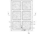
図1(a)〜図1(e)は、第一の可視光透過性電磁波吸収フィルムの一例を示す。この電磁波吸収フィルムでは、プラスチックフィルム10b上に可視光透過性金属薄膜11aが設けられた実質的に正方形状の導電複合フィルム片1aが、互いに絶縁された状態で、プラスチックフィルム10aの一面に多数配置されており、各導電複合フィルム片1aの金属薄膜11aの全面に多数の実質的に平行で断続的な線状痕12が直交するように形成されている。なお説明のために、図1(a)では、線状痕12の長さ、幅及び間隔を実際より誇張している。プラスチックフィルム10aと、導電複合フィルム片1aのプラスチックフィルム10bとの間に透明接着層14が設けられている。プラスチックフィルム10a及び10bは融着されていてもよい。導電複合フィルム片1aの金属薄膜11a側がプラスチックフィルム10aに接着されていてもよい。導電複合フィルム片1aの配列及び各導電複合フィルム片1aの向きは図示の例に限定されず、例えばランダムであってもよい。
[1] Visible light transmissive electromagnetic wave absorbing film
(1) First Visible Light Transmitting Electromagnetic Wave Absorbing Film FIGS. 1 (a) to 1 (e) show an example of the first visible light transmitting electromagnetic wave absorbing film. In this electromagnetic wave absorbing film, a plurality of substantially square conductive composite film pieces 1a each having a visible light transmissive metal
図2は第一の可視光透過性電磁波吸収フィルムの別の例を示す。この電磁波吸収フィルムでは、導電複合フィルム片1aの代わりに、プラスチックフィルム10aの一面に、多数の実質的に正方形状の可視光透過性金属薄膜11aが直接設けられており、透明接着層14を有さない以外図1に示すものと同じである。
FIG. 2 shows another example of the first visible light transmitting electromagnetic wave absorbing film. In this electromagnetic wave absorbing film, instead of the conductive composite film piece 1a, a large number of substantially square-shaped visible light transmissive metal
線状痕12を有する正方形状金属薄膜11aは、少なくとも一方、好ましくは両方の辺方向X,Y(図1(a)参照)において、自由空間の特性インピーダンス(377Ω)に近い377±250Ωの電気抵抗を有するように形成される。そのため第一の電磁波吸収フィルムは、優れた電磁波吸収能を有する。この電気抵抗は377±200Ωが好ましい。ただし金属薄膜11aは正方形状に限定されず、少なくとも一方の辺方向において377±250Ωの電気抵抗を有する限り、矩形状でもよい。金属薄膜11aの電気抵抗は、金属薄膜11aの材料、厚さ、線状痕12の幅、間隔及び長さ等を選択することにより調整することができる。
The square-shaped metal
電気抵抗は直流二端子法で測定する。正方形状の金属薄膜11aの辺方向X,Yにおける電気抵抗RX(Ω),RY(Ω)は、各々辺方向X,Yにおけるシート抵抗RsX(Ω/□),RsY(Ω/□)と等しい。矩形状の金属薄膜11aの電気抵抗RX(Ω),RY(Ω)は、各々式:RX=RsX×LX/LY[ただしLX,LYはそれぞれ金属薄膜11aの辺方向X,Yにおける長さを表す]、及び式:RY=RsY×LY/LXで表される。
Electrical resistance is measured by the DC two-terminal method. The electric resistances R X (Ω) and R Y (Ω) in the side directions X and Y of the square metal
(a) プラスチックフィルム
プラスチックフィルム10a及び10bを形成する樹脂は、絶縁性とともに十分な強度、可撓性及び加工性を有する限り特に制限されず、例えばポリエステル(ポリエチレンテレフタレート等)、ポリアリーレンサルファイド(ポリフェニレンサルファイド等)、ポリアミド、ポリイミド、ポリアミドイミド、ポリエーテルサルフォン、ポリエーテルエーテルケトン、ポリカーボネート、アクリル樹脂、ポリスチレン、ポリオレフィン(ポリエチレン、ポリプロピレン等)等が挙げられる。プラスチックフィルム10a及び10bの厚さは各々10〜100μm程度で良い。
(a) Plastic film The resin forming the
(b) 可視光透過性金属薄膜
可視光透過性金属薄膜11aを形成する金属は導電性を有する限り特に限定されないが、耐食性及びコストの観点からアルミニウム、銅、ニッケル、コバルト、銀及びこれらの合金が好ましく、特にアルミニウム、ニッケル及びこれらの合金が好ましい。金属薄膜11aの厚さは10〜100 nmが好ましい。この厚さが10 nm未満だと、膜の均一性が悪く、電磁波吸収能が低い。一方100 nm超だと、可視光透過性が悪い。ニッケル膜の場合、その厚さは20〜70 nmがより好ましい。アルミニウム膜の場合、その厚さは30〜100 nmがより好ましい。可視光透過性金属薄膜11aは蒸着膜であるのが好ましい。優れた電磁波吸収能を得るために、金属薄膜11aの合計面積率は70%以上が好ましく、80%以上がより好ましい。
(b) Visible light transmissive metal thin film The metal forming the visible light transmissive metal
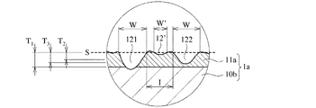
(c) 線状痕
顕微鏡写真を図式化した図1(c)及び図1(d)から明らかなように、金属薄膜11aに多数の実質的に平行な線状痕12が直交するように形成されている。なお説明のために、図1(d)では、一方向の線状痕12について、その配向方向に対して直角に切った切り口のみを示し、線状痕12の深さを実際より誇張している。線状痕12の長さ、幅及び間隔は不規則であり、非常に細い線状痕から非常に太い線状痕まで、種々の間隔で不規則に配列している。図1(d)及び図1(e)に示すように、線状痕12には、金属薄膜11aを貫通して非導通部121を形成しているものと、貫通していないが比較的深く設けられて高抵抗部122を形成しているものとがある。図1(e)に示すように、線状高抵抗部122の底部は、金属薄膜11の厚さT1の少なくとも約50%に相当する深さT2に達しているのが好ましく、約70%に相当する深さT3に達しているのがより好ましい。この例では線状非導通部121及び線状高抵抗部122の両方が形成されているが、これらのうちの一方のみが形成されていてもよい。すなわち、線状非導通部121及び/又は線状高抵抗部122により隔てられた不定形導体が不規則に接続していると見ることができる。図1(c)は不定形導体の接続部の一例(G)を示す。このような不定形導体の不規則な接続により、種々の周波数の電磁波ノイズを効率良く吸収することができる。
(c) Linear traces As can be seen from FIGS. 1 (c) and 1 (d), the micrographs are formed so that a number of substantially parallel
後述するように線状痕12は、プラスチックフィルム上の金属薄膜を、高硬度微粒子をランダムに有するパターンロールで摺接することにより形成される。従って、図1(c)〜図1(e)に示すように線状痕12は不規則に分布しているだけでなく、線状痕12の形成の際に金属薄膜は一部塑性変形し、線状痕12はテーパ状の断面を有するだけでなく、その両側が盛り上がっているので、線状痕12の幅及び間隔は厚さ方向の位置により異なる。客観的な比較を可能にするために、線状痕12の幅Wは元の表面Sと交差する位置で求め、隣接する線状痕12の間隔Iは元の表面Sと交差する位置で求める。
As will be described later, the
図1(e)に示すように、比較的浅い線状痕12’もあるが、その幅W’は幅Wより著しく小さい。また稀に並外れて幅広い線状痕が形成されることがある。金属薄膜11aの断面観察の結果、このように著しく狭い線状痕12’や並外れて幅広い線状痕は線状痕の全数の10%未満であることが分った。従って、線状痕の90%以上について幅Wの範囲を求めれば良い。その結果、線状痕12の90%以上が0.1〜1,000μmの範囲内の幅Wを有するのが好ましいことが分った。0.1μm未満又は1,000μm超の幅の線状痕12は、電磁波ノイズの吸収にほとんど寄与しない。線状痕12の90%以上の幅Wは0.1〜100μmの範囲内にあるのがより好ましく、0.1〜20μmの範囲内にあるのが最も好ましい。また線状痕12の90%以上の間隔Iも0.1〜1,000μmの範囲内にあるのが好ましく、0.1〜100μmの範囲内にあるのがより好ましく、0.1〜20μmの範囲内にあるのが最も好ましい。
As shown in FIG. 1 (e), there is a relatively shallow linear mark 12 ', but its width W' is significantly smaller than the width W. In addition, unusually wide linear traces may be formed. As a result of cross-sectional observation of the metal
線状痕12の平均幅Wav及び平均間隔Iavは、それぞれ0.1〜1,000μmの上記範囲内の幅及び間隔を平均した値である。線状痕12の平均幅Wavは1〜100μmが好ましく、1〜20μmがより好ましく、1〜10μmが最も好ましい。線状痕12の平均間隔Iavは1〜100μmが好ましく、1〜20μmがより好ましく、1〜10μmが最も好ましい。平均幅Wav及び平均間隔Iavがそれぞれ1μm未満又は10μm超であると、十分な電磁波ノイズの吸収能が得られない。
The average width Wav and the average interval Iav of the
線状痕12の長さLは、摺接条件(主としてパターンロール及びフィルムの相対的な周速、及びフィルムのパターンロールへの巻回角度)により決まるので、摺接条件を変えない限り大部分がほぼ同じである(ほぼ平均長さに等しい)。線状痕12の平均長さLavは特に限定的でなく、実用的には1〜100 mm程度で良い。
Since the length L of the
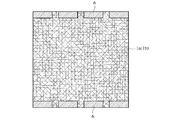
図3(a)〜図3(d)は線状痕12のパターンの別の例をそれぞれ示す。線状痕12の形成は、通常長尺の複合フィルム(少なくとも一面に金属薄膜を形成したプラスチックフィルム)に対して行うが、パターンロールの数や軸線方向を適宜設定することにより、図3(a)〜図3(d)に示すように、配向の方向及び数が異なる種々のパターンの線状痕12が得られる。特に図1(c)及び図3(a)〜図3(c)に示すように、複数方向に線状痕12を形成すると、電磁波吸収能に異方性が実質的にない電磁波吸収フィルムが得られる。
3 (a) to 3 (d) show other examples of the pattern of the
(d) 微細穴
図4(a)及び図4(b)は第一の可視光透過性電磁波吸収フィルムのさらに別の例を示す。この例では、金属薄膜11aに線状痕12の他に、多数の微細穴13がランダムに設けられている。図示の例では微細穴13は金属薄膜11aを貫通しているが、微細穴13は必ずしも金属薄膜11aを貫通していなくてもよい。微細穴13は、線状痕12の場合と同様に表面に高硬度微粒子を有するパターンロールを金属薄膜に押圧することにより形成される。貫通穴を形成するためには、高硬度微粒子の平均直径は金属薄膜の厚さの約2倍以上ある必要があり、実用的には高硬度微粒子の平均直径は金属薄膜の厚さより十分に大きい。
(d) Fine hole FIGS. 4 (a) and 4 (b) show still another example of the first visible light-transmitting electromagnetic wave absorbing film. In this example, a large number of
微細穴13の開口径Dは元の表面Sと交差する位置で求める。金属薄膜11aの厚さによるが、一般に微細穴13の開口径Dは90%以上が0.1〜1,000μmの範囲内にあるのが好ましく、0.1〜500μmの範囲内にあるのがより好ましい。また微細穴13の平均開口径Davは0.5〜100μmの範囲内にあるのが好ましく、1〜50μmの範囲内にあるのがより好ましい。平均開口径Davの上限は20μmがさらに好ましく、10μmが最も好ましい。微細穴13の平均密度は500個/cm2以上であるのが好ましく、1×104〜3×105個/cm2であるのがより好ましく、1×104〜2×105個/cm2であるのが最も好ましい。
The opening diameter D of the
(e) 保護層
図5に示すように、電磁波吸収フィルムの可視光透過性金属薄膜11aを有する面を覆うようにプラスチック保護層10cを形成しても良い。プラスチック保護層10cは、電磁波吸収フィルムの可視光透過性金属薄膜11aを有する面に、プラスチックフィルムを熱ラミネート法等で接着することにより形成できる。プラスチック保護層10cの厚さは10〜100μmが好ましい。
(e) Protective Layer As shown in FIG. 5, a plastic
(f) エンボス
電磁波ノイズの吸収能をさらに向上するために、可視光透過性電磁波吸収フィルムに円錐状、球面状等の多数のエンボスを施しても良い。エンボスの直径及び深さはそれぞれ100μm以上が好ましく、150〜250μmがより好ましい。エンボスの面積率は20〜60%が好ましい。
(f) Embossing In order to further improve the ability to absorb electromagnetic wave noise, the visible light-transmitting electromagnetic wave absorbing film may be subjected to a number of embossments such as a conical shape and a spherical shape. The emboss diameter and depth are each preferably 100 μm or more, more preferably 150 to 250 μm. The area ratio of embossing is preferably 20 to 60%.
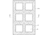
(2) 第二の可視光透過性電磁波吸収フィルム
図6(a)及び図6(b)は、本発明の第二の可視光透過性電磁波吸収フィルムの一例を示す。この電磁波吸収フィルムは、プラスチックフィルム10d上に可視光透過性金属薄膜11bが設けられ、かつ多数の透光用開口部15を有する格子状の導電複合フィルム1bが、導電複合フィルム片1aの代わりに、プラスチックフィルム10aの一面に設けられており、金属薄膜11bの全面に線状痕12が形成されている以外、図1(a)〜図1(e)に示す電磁波吸収フィルムと同じである。
(2) Second Visible Light Transmitting Electromagnetic Wave Absorbing Film FIGS. 6 (a) and 6 (b) show an example of the second visible light transmitting electromagnetic wave absorbing film of the present invention. In this electromagnetic wave absorbing film, a lattice-shaped conductive composite film 1b having a visible light-transmitting metal
図7は第二の可視光透過性電磁波吸収フィルムの別の例を示す。この電磁波吸収フィルムでは、導電複合フィルム1bの代わりに、プラスチックフィルム10aの一面に、格子状の可視光透過性金属薄膜11bが直接設けられており、透明接着層14を有さない以外、図6(a)及び図6(b)に示す電磁波吸収フィルムと同じである。
FIG. 7 shows another example of the second visible light transmitting electromagnetic wave absorbing film. In this electromagnetic wave absorbing film, instead of the conductive composite film 1b, a lattice-like visible light transmissive metal
優れた可視光透過性と電磁波吸収能とを両立するために、可視光透過性金属薄膜11bの面積率は40〜80%とするのが好ましい。可視光透過性金属薄膜11bは格子状に限定されず、多数の透光用開口部15を有する限り任意の形状とすることができる。線状痕12は第一の可視光透過性電磁波吸収フィルムと同じでよい。第二の可視光透過性電磁波吸収フィルムも、微細穴13、プラスチック保護層10c及びエンボスを有してもよい。これらは第一の可視光透過性電磁波吸収フィルムについて説明したものと同じで良い。
In order to achieve both excellent visible light transparency and electromagnetic wave absorption capability, the area ratio of the visible light transmissive metal
金属薄膜11bのシート抵抗(金属薄膜11bが正方形状となるように電磁波吸収フィルムを任意のサイズで切り取ったサンプルの両方の辺方向における電気抵抗。直流二端子法で測定。)は377±250Ω/□が好ましく、377±200Ω/□がより好ましい。
Sheet resistance of the metal
(3) 第三の可視光透過性電磁波吸収フィルム
図8(a)及び図8(b)は、本発明の第三の可視光透過性電磁波吸収フィルムの一例を示す。この電磁波吸収フィルムは、多数の導電複合フィルム片1aと、導電複合フィルム1bとを有し、各導電複合フィルム片1aが導電複合フィルム1bの各開口部15の中に位置し、かつ絶縁した状態で配置されている以外、図1(a)〜図1(e)に示す電磁波吸収フィルムと同じである。図示の例では、導電複合フィルム片1a及び導電複合フィルム1b(以下両者を纏めて「導電複合フィルム1a,1b」とよぶ)の両方に線状痕12が形成されているが、線状痕12は、導電複合フィルム1a,1bの一方のみに形成されていてもよい。
(3) Third Visible Light Transmitting Electromagnetic Wave Absorbing Film FIGS. 8 (a) and 8 (b) show an example of the third visible light transmitting electromagnetic wave absorbing film of the present invention. This electromagnetic wave absorbing film has a large number of conductive composite film pieces 1a and conductive composite films 1b, and each conductive composite film piece 1a is located in each opening 15 of the conductive composite film 1b and insulated. 1 is the same as the electromagnetic wave absorbing film shown in FIGS. 1 (a) to 1 (e). In the illustrated example, the
図9は第三の可視光透過性電磁波吸収フィルムの別の例を示す。この電磁波吸収フィルムでは、導電複合フィルム1a,1bの代わりに、プラスチックフィルム10aの一面に、正方形状又は矩形状の可視光透過性金属薄膜11a、及び開口部15を有する可視光透過性金属薄膜11bが各々直接設けられており、透明接着層14を有さない以外図8(a)及び図8(b)に示すものと同じである。
FIG. 9 shows another example of the third visible light transmitting electromagnetic wave absorbing film. In this electromagnetic wave absorbing film, instead of the conductive composite films 1a and 1b, a visible light transmissive metal
電磁波ノイズを効率良く吸収するため、金属薄膜11a,11bの一方を上記磁性金属で形成し、他方を上記非磁性金属で形成してもよい。好ましい組合せはニッケルとアルミニウムである。優れた電磁波吸収能を得るために、金属薄膜11a,11bの合計面積率は70%以上が好ましく、80%以上がより好ましい。線状痕12は第一の可視光透過性電磁波吸収フィルムと同じでよい。
In order to efficiently absorb electromagnetic wave noise, one of the metal
第三の可視光透過性電磁波吸収フィルムも、微細穴13、プラスチック保護層10c及びエンボスを有してもよい。これらは第一の可視光透過性電磁波吸収フィルムについて説明したものと同じで良い。
The third visible light transmitting electromagnetic wave absorbing film may also have the fine holes 13, the plastic
[2] 可視光透過性電磁波吸収フィルムの製造方法
(1) 間接法
図1(a)〜図1(e)に示すような、導電複合フィルム片1aを有する第一の可視光透過性電磁波吸収フィルムは、可視光透過性金属薄膜11Aとプラスチックフィルム10Bとからなる導電複合フィルム1Aを形成し、導電複合フィルム1Aに線状痕を形成し、線状痕付き導電複合フィルム1A'をカットして正方形状又は矩形状の導電複合フィルム片1aを形成し、導電複合フィルム片1aをプラスチックフィルム10aの少なくとも一面に配置し、積層する間接法により製造することができる。
[2] Manufacturing method of visible light transmitting electromagnetic wave absorbing film
(1) Indirect method As shown in FIGS. 1 (a) to 1 (e), the first visible light transmitting electromagnetic wave absorbing film having the conductive composite film piece 1a includes a visible light transmitting metal
図6(a)及び図6(b)に示すような、導電複合フィルム1bを有する第二の可視光透過性電磁波吸収フィルムは、可視光透過性金属薄膜11Bとプラスチックフィルム10Dとからなる導電複合フィルム1Bを形成し、導電複合フィルム1Bに線状痕を形成し、線状痕付き導電複合フィルム1B'をカットして開口部15を有する導電複合フィルム1bを形成し、導電複合フィルム1bをプラスチックフィルム10aの少なくとも一面に配置し、積層する間接法により製造することができる。
6 (a) and 6 (b), the second visible light transmissive electromagnetic wave absorbing film having the conductive composite film 1b is a conductive composite made of a visible light transmissive metal
図8(a)及び図8(b)に示すような、導電複合フィルム片1a及び導電複合フィルム1bを有する第三の可視光透過性電磁波吸収フィルムは、上記の第一及び第二の可視光透過性電磁波吸収フィルムの製造方法を組合せることにより、製造することができる。 The third visible light transmitting electromagnetic wave absorbing film having the conductive composite film piece 1a and the conductive composite film 1b as shown in FIG. It can manufacture by combining the manufacturing method of a transparent electromagnetic wave absorption film.
(a) 導電複合フィルムの形成
(i) 金属薄膜の形成
金属の蒸着は、例えば真空蒸着法、スパッタリング法、イオンプレーティング法等の物理蒸着法、プラズマCVD法、熱CVD法、光CVD法等の化学気相蒸着法等により行うことができる。
(a) Formation of conductive composite film
(i) Formation of metal thin film Metal deposition is performed by, for example, physical vapor deposition such as vacuum vapor deposition, sputtering, or ion plating, chemical vapor deposition such as plasma CVD, thermal CVD, or photo-CVD. It can be carried out.
(ii) 線状痕の形成
(ii-1) 線状痕形成装置
図1(c)及び図3(a)〜図3(c)に示すような複数方向に配向する線状痕12は、プラスチックフィルム10B(10D)に形成した金属薄膜11A(11B)に、多数の高硬度の微粒子を表面に有し、軸線方向が異なる複数のパターンロールを摺接させる装置を用いて形成することができる。
(ii) Formation of linear marks
(ii-1) Linear trace forming apparatus Linear traces 12 oriented in a plurality of directions as shown in FIGS. 1 (c) and 3 (a) to 3 (c) are formed on a
図10(a)〜図10(e)は、図1(c)及び図3(c)に示すような直交する線状痕を形成する装置の例を示す。この線状痕形成装置は上流側から順に、(1) プラスチックフィルム10B(10D)の一面に金属薄膜11A(11B)が形成された複合フィルム1A(1B)を巻き出すリール21と、(2) 複数のガイドロール22と、(3) 多数の高硬度の微粒子を表面に有し、複合フィルム1A(1B)の幅方向と異なる方向で金属薄膜11A(11B)の側に配置された第一のパターンロール2aと、(4) 第一のパターンロール2aの上流側で、金属薄膜11A(11B)の反対側に配置された第一の押えロール3aと、(5) 多数の高硬度の微粒子を表面に有し、複合フィルム1A(1B)の幅方向に関して第一のパターンロール2aと逆方向に、かつ金属薄膜11A(11B)の側に配置された第二のパターンロール2bと、(6) 第二のパターンロール2bの下流側で、金属薄膜11A(11B)の反対側に配置された第二の押えロール3bと、(7) 第一及び第二のパターンロール2a,2bの間で、金属薄膜11A(11B)の側に配置された電気抵抗測定手段4aと、(8) 第二のパターンロール2bの下流側で、金属薄膜11A(11B)の側に配置された電気抵抗測定手段4bと、(9) 複数のガイドロール23と、(10) 線状痕を形成した複合フィルム1A'(1B')を巻き取るリール24とを有する。各パターンロール2a,2bは、微小な撓みを防止するためにバックアップロール5a,5bで支持されている。バックアップロール5a,5bは、パターンロール2a,2bに悪影響を与えないようにゴムロールが好ましい。
FIG. 10 (a) to FIG. 10 (e) show an example of an apparatus for forming orthogonal linear marks as shown in FIG. 1 (c) and FIG. 3 (c). This linear mark forming apparatus is, in order from the upstream side, (1) a
図10(c)に示すように、複合フィルム1A(1B)の金属薄膜11A(11B)が押圧された状態で各パターンロール2a,2bと摺接するように、各押えロール3a,3bの縦方向位置は複合フィルム1A(1B)と各パターンロール2a,2bとの摺接位置より低い。この条件を満たしたまま各押えロール3a,3bの縦方向位置を調整することにより、金属薄膜11A(11B)の各パターンロール2a,2bへの押圧力を調整するとともに、中心角θ1により表される摺接距離を調整することができる。
As shown in FIG. 10 (c), the vertical direction of each
図10(d)は線状痕12aが複合フィルム1A(1B)の進行方向に対して斜めに形成される原理を示す。複合フィルム1A(1B)の進行方向に対してパターンロール2aは傾斜しているので、パターンロール2a上の硬質微粒子の移動方向(回転方向)aと複合フィルム1A(1B)の進行方向bとは異なる。そこで三角形Xで示すように、任意の時点においてパターンロール2a上の点Aにおける硬質微粒子が複合フィルム1A(1B)の金属薄膜と接触して痕Bが形成されたとすると、所定の時間後に硬質微粒子は点A’まで移動し、痕Bは点B’まで移動する。点Aから点A’まで硬質微粒子が移動する間、痕は連続的に形成されるので、点B’から点A’まで延在する線状痕12aが形成されたことになる。
FIG. 10 (d) shows the principle that the
第一及び第二のパターンロール2a,2bで形成される第一及び第二の線状痕群12A,12Bの方向及びそれらの交差角は、各パターンロール2a,2bの複合フィルム1A(1B)に対する角度、及び/又は複合フィルム1A(1B)の走行速度に対する各パターンロール2a,2bの周速度を調整することにより調整することができる。例えば、複合フィルム1A(1B)の走行速度bに対するパターンロール2aの周速度aを増大させると、図10(d)の三角形Yで示すように線状痕12aを線分C’D’のように複合フィルム1A(1B)の進行方向に対して45°にすることができる。同様に、複合フィルム1A(1B)の幅方向に対するパターンロール2aの傾斜角θ2を変えると、パターンロール2aの周速度aを変えることができる。これはパターンロール2bについても同様である。従って、両パターンロール2a,2bの調整により、線状痕12a,12bの方向を図1(c)及び図3(c)に例示するように変更することができる。
The directions of the first and second
各パターンロール2a,2bは複合フィルム1A(1B)に対して傾斜しているので、各パターンロール2a,2bとの摺接により複合フィルム1A(1B)は幅方向の力を受け、蛇行するおそれがある。複合フィルム1A(1B)の蛇行を防止するために、各パターンロール2a,2bに対する各押えロール3a,3bの縦方向位置及び/又は角度を調整するのが好ましい。例えば、パターンロール2aの軸線と押えロール3aの軸線との交差角θ3を適宜調節すると、幅方向の力をキャンセルするように押圧力の幅方向分布が得られ、もって蛇行を防止することができる。またパターンロール2aと押えロール3aとの間隔の調整も蛇行の防止に寄与する。
Since each
複合フィルム1A(1B)の蛇行及び破断を防止するために、第一及び第二のパターンロール2a,2bの回転方向は複合フィルム1A(1B)の進行方向と同じであるのが好ましい。
In order to prevent meandering and breakage of the
図10(b)に示すように、各電気抵抗測定手段(ロール)4a,4bは絶縁部40を介して両端部に一対の電極41,41を有し、電極41,41間において線状痕12a,12bを有する金属薄膜11A(11B)の電気抵抗を測定する。電気抵抗測定ロール4a,4bで測定した電気抵抗値を目標の電気抵抗値と比較し、それらの差に応じて運転条件を調整する。調整される運転条件は、複合フィルム1A(1B)の走行速度、パターンロール2a,2bの回転速度及び傾斜角θ2、押えロール3a,3bの縦方向位置、パターンロール2a,2bからの距離、及びパターンロール2a,2bからの傾斜角θ3等である。
As shown in FIG. 10 (b), each electrical resistance measuring means (roll) 4a, 4b has a pair of
図11に示すようにパターンロール2a,2bの間に第三の押えロール3cを設けると、複合フィルム1A(1B)の金属薄膜11A(11B)がパターンロール2a,2bに押圧される力が増大するだけでなく、中心角θ1により表される金属薄膜11A(11B)の摺接距離が増大し、線状痕12a,12bの深さ及び幅が大きくなる。その上、複合フィルム1A(1B)の蛇行の防止にも寄与する。
As shown in FIG. 11, when the
図12は、図3(a)に示すような三方向に配向する線状痕を形成する装置の例を示す。この装置は、第二のパターンロール2bの下流側に複合フィルム1A(1B)の幅方向に配置された第三のパターンロール2cを設けた以外、図10(a)〜図10(e)に示す装置と同じである。第三のパターンロール2cの回転方向は複合フィルム1A(1B)の進行方向と同じでも逆でも良い。幅方向に配置された第三のパターンロール2cは複合フィルム1A(1B)の進行方向に延在する線状痕12cを形成する。第三の押えロール30bは第三のパターンロール2cの上流側でも下流側でも良い。勿論、第三のパターンロール2cの下流側に電気抵抗測定ロール4cを設けても良い。
FIG. 12 shows an example of an apparatus for forming linear traces oriented in three directions as shown in FIG. 3 (a). This apparatus is shown in FIGS. 10 (a) to 10 (e) except that a
図13は、図3(b)に示すような四方向に配向する線状痕を形成する装置の例を示す。この装置は、第二のパターンロール2bと第三のパターンロール2cとの間に第四のパターンロール2dを設け、第四のパターンロール2dの上流側に第四の押えロール3dを設けた以外、図12に示す装置と同じである。第四のパターンロール2dの回転速度を遅くすることにより、図10(d)における三角形Zで示すように、線状痕12a'の方向(線分E’F’)を複合フィルム1A(1B)の幅方向にすることができる。
FIG. 13 shows an example of an apparatus for forming linear traces oriented in four directions as shown in FIG. 3 (b). This apparatus is provided with a
図14は、図3(c)に示すような直交する線状痕を形成する装置の別の例を示す。この線状痕形成装置は、基本的に第二のパターンロール32bが複合フィルム1A(1B)の幅方向に配置されている点で図10(a)〜図10(e)に示す装置と異なる。従って、図10(a)〜図10(e)に示す装置と異なる部分のみ以下説明する。第二のパターンロール32bの回転方向は複合フィルム1A(1B)の進行方向と同じでも逆でも良い。また第二の押えロール33bは第二のパターンロール32cの上流側でも下流側でも良い。この装置は、図10(d)における三角形Zで示すように、線状痕12a'の方向(線分E’F’)を複合フィルム1A(1B)の幅方向にし、図3(c)に示す線状痕を形成するのに適している。
FIG. 14 shows another example of an apparatus for forming orthogonal linear marks as shown in FIG. 3 (c). This linear scar forming apparatus is basically different from the apparatus shown in FIGS. 10 (a) to 10 (e) in that the
図15は、図3(d)に示すような一方向に配向する線状痕を形成する装置の例を示す。この線状痕形成装置は、複合フィルム1A(1B)の幅方向に配置されたパターンロール42のみを有する以外、図14に示す装置と同じである。パターンロール42は複合フィルム1A(1B)の進行方向に延在する線状痕12b'を形成する。押えロール43はパターンロール42の上流側でも下流側でも良い。パターンロール42の上流側及び下流側に電気抵抗測定ロール44a及び44bを設けても良い。
FIG. 15 shows an example of an apparatus for forming linear traces oriented in one direction as shown in FIG. 3 (d). This linear trace forming apparatus is the same as the apparatus shown in FIG. 14 except that it has only the pattern roll 42 arranged in the width direction of the
(ii-2) 運転条件
線状痕の傾斜角及び交差角だけでなく、それらの深さ、幅、長さ及び間隔を決める運転条件としては、複合フィルムの走行速度、パターンロールの回転速度及び傾斜角θ2、複合フィルムの張力(押えロールの縦方向位置、パターンロールからの距離、及びパターンロールからの傾斜角θ3等により決まる。)等である。複合フィルムの走行速度は5〜200 m/分が好ましく、パターンロールの回転速度(周速)は10〜2,000 m/分が好ましい。傾斜角θ2は20°〜60°が好ましく、特に約45°が好ましい。複合フィルムの張力は0.05〜5kgf/cm幅が好ましい。
(ii-2) Operating conditions As well as the inclination angle and crossing angle of the linear traces, the operating conditions for determining the depth, width, length and interval of these are the traveling speed of the composite film, the rotational speed of the pattern roll, and The inclination angle θ 2 , the tension of the composite film (determined by the longitudinal position of the press roll, the distance from the pattern roll, the inclination angle θ 3 from the pattern roll, etc.) and the like. The traveling speed of the composite film is preferably 5 to 200 m / min, and the rotational speed (peripheral speed) of the pattern roll is preferably 10 to 2,000 m / min. The inclination angle θ 2 is preferably 20 ° to 60 °, and particularly preferably about 45 °. The tension of the composite film is preferably 0.05 to 5 kgf / cm width.
(ii-3) パターンロール
線状痕形成装置に使用するパターンロールは、特開2002-59487号に記載されているダイヤモンドロールが好ましい。線状痕の幅は微粒子の粒径により決まるので、ダイヤモンド微粒子の90%以上は1〜1,000μmの範囲内の粒径を有するのが好ましく、10〜200μmの範囲内の粒径がより好ましい。ダイヤモンド微粒子はロール面に50%以上の面積率で付着しているのが好ましい。
(ii-3) Pattern roll The pattern roll used in the linear trace forming apparatus is preferably a diamond roll described in JP-A-2002-59487. Since the width of the linear mark is determined by the particle size of the fine particles, 90% or more of the diamond fine particles preferably have a particle size in the range of 1 to 1,000 μm, and more preferably in the range of 10 to 200 μm. The diamond fine particles are preferably attached to the roll surface at an area ratio of 50% or more.
(iii) 微細穴の形成
特許第2063411号等に記載の方法により金属薄膜11A(11B)に多数の微細穴13を形成することができる。例えば、鋭い角部を有するモース硬度5以上の多数の微粒子が表面に付着した第一ロール(上記線状痕形成用ロールと同じで良い)と、第一ロールに押圧された平滑な第二ロールとの間隙に、金属薄膜11A(11B)を第一ロールの側にして、複合フィルム1A(1B)を通過させる。微細穴13の平均開口径、平均面積率及び深さは、第一ロールの微粒子の粒径及び面積率並びに押圧力等により調整できる。
(iii) Formation of fine holes A large number of
(b) 線状痕付き導電複合フィルムのカット
線状痕付き導電複合フィルム1A'(1B')を、打ち抜き等によりカットし、実質的に正方形状又は矩形状の導電複合フィルム片1a、及び/又は開口部15を有する導電複合フィルム1bを形成する。
(b) Cut of conductive composite film with linear traces Cut conductive
(c) 積層
透明接着層14を用いるか、融着することにより、導電複合フィルム片1a及び/又は導電複合フィルム1bを、プラスチックフィルム10aに積層する。
(c) Lamination The conductive composite film piece 1a and / or the conductive composite film 1b are laminated on the
(d) 保護層の形成
プラスチックフィルムを熱ラミネート法等で導電複合フィルム片1a及び/又は導電複合フィルム1bに接着することにより、プラスチック保護層10cを形成することができる。
(d) Formation of Protective Layer The plastic
(e) エンボス加工
上記積層工程を行い、必要に応じて保護層10cを設けた後、円錐状、球面状等の多数の突起を有するロール等を用いてエンボス加工する。
(e) Embossing After the above lamination process is performed and a
(2) 直接法
図2、7及び9に示すような、可視光透過性金属薄膜11a及び/又は11bがプラスチックフィルム10a上に直接設けられた可視光透過性電磁波吸収フィルムは、(a) プラスチックフィルム10aの少なくとも一面に、蒸着法により一様に金属薄膜11A(11B)を形成し、意図する金属薄膜11aの形状(正方形状もしくは矩形状)、及び/又は意図する金属薄膜11bの形状(例えば格子状)となるようにフォトレジストを塗布し、露光後エッチングした後、線状痕12を形成するか、(b) プラスチックフィルム10aにおいて金属薄膜11aを形成しない部分、及び/又は金属薄膜11bを形成しない部分(透光用開口部15を形成する部分)に、あらかじめフォトレジストを塗布し、露光後、蒸着法により金属薄膜11a及び/又は11bを形成し、フォトレジスト層を除去した後、線状痕12を形成する直接法により、形成できる。線状痕、微細穴、保護層の形成及びエンボス加工はいずれも上記と同じでよい。
(2) Direct method As shown in FIGS. 2, 7 and 9, the visible light transmitting electromagnetic wave absorbing film in which the visible light transmitting metal
[3] 可視光透過性電磁波吸収フィルムの特性
本発明の可視光透過性を有する第一〜第三の電磁波吸収フィルムは、多数の断続的で不規則な線状痕により、種々の周波数を有する電磁波ノイズを吸収することができる。特に複数方向に(好ましくは直交するように)線状痕12が形成された電磁波吸収フィルムは、電磁波ノイズの吸収能に異方性が少なく、優れた電磁波ノイズの吸収能を有する。
[3] Properties of Visible Light Transmitting Electromagnetic Wave Absorbing Film The first to third electromagnetic wave absorbing films having visible light transmissivity of the present invention have various frequencies due to a large number of intermittent irregular traces. Electromagnetic noise can be absorbed. In particular, the electromagnetic wave absorbing film in which the
[4] 可視光透過性電磁波吸収体
(1) 構造
(a) 第一の可視光透過性電磁波吸収体
本発明の第一の可視光透過性電磁波吸収体は、複数枚の可視光透過性電磁波吸収フィルムを間に空間を設けて又は設けないで積層してなる。空間を設けないで積層する場合、必要に応じて接着してもよい。複数枚の可視光透過性電磁波吸収フィルムの組合せには、複数枚の第一の電磁波吸収フィルムからなる場合と、複数枚の第二の電磁波吸収フィルムからなる場合と、複数枚の第三の電磁波吸収フィルムからなる場合と、少なくとも1枚の第一の電磁波吸収フィルムと少なくとも1枚の第二の電磁波吸収フィルムの組合せからなる場合と、少なくとも1枚の第一の電磁波吸収フィルムと少なくとも1枚の第三の電磁波吸収フィルムの組合せからなる場合と、少なくとも1枚の第二の電磁波吸収フィルムと少なくとも1枚の第三の電磁波吸収フィルムの組合せからなる場合と、少なくとも1枚の第一の電磁波吸収フィルムと少なくとも1枚の第二の電磁波吸収フィルムと少なくとも1枚の第三の電磁波吸収フィルムの組合せからなる場合等がある。
[4] visible light transmissive electromagnetic wave absorber
(1) Structure
(a) First visible light transmissive electromagnetic wave absorber The first visible light transmissive electromagnetic wave absorber of the present invention is laminated with or without a plurality of visible light transmissive electromagnetic wave absorber films. Do it. When laminating without providing a space, it may be adhered as necessary. The combination of a plurality of visible light-transmitting electromagnetic wave absorbing films includes a plurality of first electromagnetic wave absorbing films, a plurality of second electromagnetic wave absorbing films, and a plurality of third electromagnetic waves. A case comprising an absorption film, a case comprising a combination of at least one first electromagnetic wave absorption film and at least one second electromagnetic wave absorption film, and at least one first electromagnetic wave absorption film and at least one sheet. A combination of a third electromagnetic wave absorbing film, a case of a combination of at least one second electromagnetic wave absorbing film and at least one third electromagnetic wave absorbing film, and at least one first electromagnetic wave absorbing film. It may be a combination of a film, at least one second electromagnetic wave absorbing film, and at least one third electromagnetic wave absorbing film.
第一の電磁波吸収体は、少なくとも1枚の第一の電磁波吸収フィルムと、少なくとも1枚の第二の電磁波吸収フィルムとの組合せからなるのが好ましい。電磁波ノイズを効率良く吸収するため、第一の電磁波吸収フィルムの金属薄膜11a及び第二の電磁波吸収フィルムの金属薄膜11bの一方を磁性金属で形成し、他方を非磁性金属で形成するのが好ましく、金属薄膜11aを磁性金属で形成し、かつ金属薄膜11bを非磁性金属で形成するのがより好ましい。磁性金属及び非磁性金属は各々上記と同じでよい。好ましい組合せはニッケルとアルミニウムである。
The first electromagnetic wave absorber is preferably composed of a combination of at least one first electromagnetic wave absorbing film and at least one second electromagnetic wave absorbing film. In order to efficiently absorb electromagnetic wave noise, it is preferable that one of the metal
複数枚の電磁波吸収フィルムを平行に配置した電磁波吸収体の場合、優れた電磁波ノイズの吸収能を得るために、電磁波吸収フィルムの間隔は0.2〜10 mmが好ましく、1〜8mmがより好ましい。 In the case of an electromagnetic wave absorber in which a plurality of electromagnetic wave absorbing films are arranged in parallel, the distance between the electromagnetic wave absorbing films is preferably 0.2 to 10 mm, and more preferably 1 to 8 mm, in order to obtain excellent electromagnetic wave noise absorbing ability.
(b) 第二の可視光透過性電磁波吸収体
本発明の第二の可視光透過性電磁波吸収体は、(i) 第一〜第三の電磁波吸収フィルムからなる群から選ばれた少なくとも一種と、(ii) 金属薄膜11aに線状痕を形成していない以外第一の電磁波吸収フィルムと同じである第一の線状痕非形成可視光透過性電磁波吸収フィルム、金属薄膜1bに線状痕を形成していない以外第二の電磁波吸収フィルムと同じである第二の線状痕非形成可視光透過性電磁波吸収フィルム、並びに金属薄膜11a及び11bに線状痕を形成していない以外第三の電磁波吸収フィルムと同じである第三の線状痕非形成可視光透過性電磁波吸収フィルムからなる群から選ばれた少なくとも一種とを、間に空間を設けて又は設けないで積層してなる。第一〜第三の線状痕非形成可視光透過性電磁波吸収フィルムの金属薄膜のシート抵抗は特に制限されない。
(b) Second visible light transmissive electromagnetic wave absorber The second visible light transmissive electromagnetic wave absorber of the present invention is (i) at least one selected from the group consisting of first to third electromagnetic wave absorbing films. (Ii) a first linear scar non-visible visible light transmitting electromagnetic wave absorbing film that is the same as the first electromagnetic wave absorbing film except that the metal
第二の電磁波吸収体は、少なくとも1枚の第二の電磁波吸収フィルムと、少なくとも1枚の第一の線状痕非形成電磁波吸収フィルムとの組合せからなるのが好ましい。電磁波ノイズを効率良く吸収するため、第二の電磁波吸収フィルムの金属薄膜11bを非磁性金属で形成し、かつ第一の線状痕非形成電磁波吸収フィルムの金属薄膜11aを磁性金属で形成するのがより好ましい。磁性金属及び非磁性金属は各々上記と同じでよい。好ましい組合せはニッケルとアルミニウムである。複数枚の電磁波吸収フィルムを平行に配置した場合の電磁波吸収フィルムの間隔は上記と同じでよい。
The second electromagnetic wave absorber is preferably composed of a combination of at least one second electromagnetic wave absorbing film and at least one first linear mark non-forming electromagnetic wave absorbing film. In order to efficiently absorb electromagnetic wave noise, the metal
(2) 特性
可視光透過性電磁波吸収フィルムは僅かながら電磁波ノイズを反射及び透過するが、反射及び透過した電磁波ノイズは別の可視光透過性電磁波吸収フィルム又は線状痕非形成可視光透過性電磁波吸収フィルムにより吸収されるので、本発明の第一及び第二の可視光透過性磁波吸収体は、極めて高い電磁波ノイズの吸収能を有する。
(2) Characteristics The visible light transmitting electromagnetic wave absorbing film slightly reflects and transmits electromagnetic noise, but the reflected and transmitted electromagnetic noise is different from the visible light transmitting electromagnetic wave absorbing film or the visible light transmitting electromagnetic wave that does not form a linear mark. Since it is absorbed by the absorbing film, the first and second visible light transmissive magnetic wave absorbers of the present invention have an extremely high electromagnetic noise absorption capability.
[5] 用途
本発明の可視光透過性を有する第一〜第三の電磁波吸収フィルム並びに第一及び第二の電磁波吸収体は、携帯電話、パーソナルコンピュータ、テレビ等の電子機器や通信機器;RFIDシステム、無線LANシステム等の通信システムにおける電磁波ノイズの漏洩及び進入の防止や、情報の漏洩防止等に適しており、電子・通信機器の筺体、建築物の壁及び窓、透明パーティション等に配置することができる。特に建築物の窓、透明パーティション等に配置すると、可視光を遮断せずに電磁波吸収能を得ることができる。
[5] Applications The first to third electromagnetic wave absorbing films and the first and second electromagnetic wave absorbers having visible light transmittance according to the present invention are electronic devices and communication devices such as mobile phones, personal computers, and televisions; RFID Suitable for prevention of leakage and intrusion of electromagnetic wave noise and information leakage in communication systems such as systems, wireless LAN systems, etc., and placed in electronic / communication equipment housings, building walls and windows, transparent partitions, etc. be able to. In particular, when it is arranged in a building window, a transparent partition or the like, it is possible to obtain electromagnetic wave absorption ability without blocking visible light.
本発明を以下の実施例によりさらに詳細に説明するが、本発明はこれらの例に限定されるものではない。 The present invention will be described in more detail with reference to the following examples, but the present invention is not limited to these examples.
実施例1
(1) 複合フィルムの作製
厚さ12μmの二軸延伸PETフィルムの一面に、真空蒸着法により厚さ50 nmのアルミニウム層を形成し、複合フィルムを作製した。
Example 1
(1) Production of
(2) 線状痕の形成
図13に示す装置を用い、粒径の分布が50〜80μmのダイヤモンド微粒子を電着したパターンロール2a〜2dに、アルミニウム層をパターンロール2a〜2dの側にして複合フィルム1Bを摺接させ、運転条件(複合フィルムの走行速度、パターンロール2a〜2dの回転速度及び傾斜角θ2、フィルムの巻回角度θ1及び複合フィルムの張力)を適宜設定することにより、図3(b)に示す四方向に配向する線状痕を形成した。得られたフィルムの線状痕の幅は0.5〜5μmの範囲であり、線状痕の平均幅は2μmであり、線状痕の間隔は2〜10μmの範囲であり、線状痕の平均間隔は5μmであり、線状痕の平均長さは5mmであった。
(2) Formation of linear traces Using the apparatus shown in FIG. 13, pattern rolls 2a to 2d electrodeposited with diamond fine particles having a particle size distribution of 50 to 80 μm and an aluminum layer on the pattern rolls 2a to 2d side By sliding the
(3) 表面抵抗の測定
表面抵抗を直流二端子法で測定した。図16に示すように、線状痕を形成した複合フィルムを15 cm×15 cmにカットした試験片の両端部に、4個ずつ銅電極(長さ3cm×幅1cm)6を配置し、対向する四対の電極6,6間の抵抗値を測定し、平均することにより、表面抵抗を求めた結果、377Ω/□であった。
(3) Measurement of surface resistance The surface resistance was measured by the DC two-terminal method. As shown in Fig. 16, four copper electrodes (length 3cm x width 1cm) 6 are arranged on both ends of the test piece obtained by cutting the composite film formed with linear marks into 15cm x 15cm. The resistance value between the four pairs of electrodes 6 and 6 was measured and averaged to obtain the surface resistance. As a result, it was 377Ω / □.
(4) 電磁波吸収フィルムの作製
線状痕を形成した複合フィルムを打ち抜き加工し、正方形状の開口部(一辺5cm)を多数有する導電複合フィルムを形成した。導電複合フィルムの両面に、二軸延伸PETフィルム(厚さ16μm)を融着させて、プラスチック保護層を有する以外図6(a)及び図6(b)に示すものと同じ第二の電磁波吸収フィルムを作製した。この電磁波吸収フィルムの金属薄膜の面積率は50%であった。
(4) Production of electromagnetic wave absorbing film A composite film having linear traces was punched out to form a conductive composite film having a large number of square openings (5 cm on a side). A second electromagnetic wave absorption similar to that shown in FIGS. 6 (a) and 6 (b) except that a biaxially stretched PET film (thickness 16 μm) is fused on both sides of the conductive composite film and a plastic protective layer is provided. A film was prepared. The area ratio of the metal thin film of this electromagnetic wave absorbing film was 50%.
(5) 電磁波ノイズの吸収能の評価
電磁波吸収フィルムの電磁波ノイズの吸収能を以下の方法により評価した。図17に示すように、発泡スチロール製サンプル台7と、送信アンテナ81と、受信アンテナ82と、アンテナ81,82を接続したネットワークアナライザ8とを有する装置を用い、ブランクとして、サンプル台7に載置したアルミニウム板(縦60 cm×横60 cm×厚さ5mm)に、3m離れたアンテナ81から、7度の入射角度θで1〜6GHzの電磁波を0.25 GHz間隔で照射し、アンテナ82で反射波を受信し、ネットワークアナライザ8により反射電力を測定した。サンプル台7に上記電磁波吸収フィルムの試験片S(縦60 cm×横60 cm)を載置し、ブランクと同様にして反射電力を測定した。ブランクの反射電力が入射電力と等しいと仮定し、反射係数RC(電磁波吸収フィルムについて測定した反射電力と入射電力との比)を求め、式:R(dB)=−20log(1/RC)に従い、反射減衰量R(dB)を求めた。結果を図18に示す。
(5) Evaluation of electromagnetic wave noise absorbing ability The electromagnetic wave absorbing ability of the electromagnetic wave absorbing film was evaluated by the following method. As shown in FIG. 17, a device having a sample table 7 made of polystyrene foam, a transmitting
実施例2
厚さ16μmの二軸延伸PETフィルムの一面に、真空蒸着法により厚さ30 nmのニッケル層を形成し、複合フィルムを作製した。複合フィルムを打ち抜き加工し、正方形状の複合フィルム片(一辺12.5 cm。図1(a)〜図1(e)に示す複合フィルム片1a。)を多数形成した。複合フィルム片のシート抵抗は、両方の辺方向とも15Ω/□であった。各複合フィルム片が互いに絶縁した状態で配置されるように、各複合フィルム片を二枚の二軸延伸PETフィルム(厚さ16μm)で挟み、融着させて、線状痕を有さない以外図1(a)及び図5に示すものと同じである第一の線状痕非形成可視光透過性電磁波吸収フィルム(金属薄膜の合計面積率90%)を作製した。
Example 2
A 30 nm thick nickel layer was formed on one side of a 16 μm thick biaxially stretched PET film by a vacuum deposition method to produce a composite film. The composite film was punched to form a large number of square-shaped composite film pieces (12.5 cm on a side. Composite film pieces 1a shown in FIGS. 1 (a) to 1 (e)). The sheet resistance of the composite film piece was 15Ω / □ in both side directions. Each composite film piece is sandwiched between two biaxially stretched PET films (thickness 16μm) and fused so that each composite film piece is placed in a state of being insulated from each other. A first linear mark non-formed visible light transmitting electromagnetic wave absorbing film (total area ratio of metal thin film 90%) which is the same as that shown in FIGS. 1 (a) and 5 was produced.
上記第一の線状痕非形成可視光透過性電磁波吸収フィルムの試験片(縦60 cm×横60 cm)と、実施例1と同じ第二の電磁波吸収フィルムの試験片(縦60 cm×横60 cm)との積層体について、電磁波ノイズの吸収能を評価した。結果を図18に示す。 A test piece (60 cm long x 60 cm wide) of the first linear mark-free visible light transmitting electromagnetic wave absorbing film and a second electromagnetic wave absorbing film test piece (60 cm long x horizontal) as in Example 1 60 cm) was evaluated for electromagnetic wave noise absorption ability. The results are shown in FIG.
実施例3
厚さ16μmの二軸延伸PETフィルムの一面に、真空蒸着法により厚さ50 nmのニッケル層を形成し、複合フィルムを作製した。この複合フィルム(シート抵抗:10Ω/□)を用いた以外実施例2と同様にして第一の線状痕非形成可視光透過性電磁波吸収フィルム(金属薄膜の合計面積率90%)を作製した。
Example 3
A 50 nm thick nickel layer was formed on one side of a 16 μm thick biaxially stretched PET film by a vacuum deposition method to produce a composite film. Except for using this composite film (sheet resistance: 10Ω / □), a first linear scar-free visible light transmitting electromagnetic wave absorbing film (total area ratio of metal thin film 90%) was prepared in the same manner as in Example 2. .
図12に示す装置を用い、粒径の分布が50〜80μmのダイヤモンド微粒子を電着したパターンロール2a〜2cに、アルミニウム層をパターンロール2a〜2cの側にして複合フィルムを摺接させ、運転条件を適宜設定することにより、図3(a)に示す三方向に配向する線状痕を形成した。得られたフィルムの線状痕の幅は0.5〜5μmの範囲であり、線状痕の平均幅は2μmであり、線状痕の間隔は2〜10μmの範囲であり、線状痕の平均間隔は5μmであり、線状痕の平均長さは5mmであった。この線状痕を有する複合フィルムのシート抵抗は200Ω/□であった。この線状痕形成複合フィルムを用いた以外実施例1と同様にして、第二の電磁波吸収フィルム(金属薄膜の面積率70%)を作製した。 Using the apparatus shown in FIG. 12, the composite film is slid in contact with the pattern rolls 2a to 2c electrodeposited with diamond fine particles having a particle size distribution of 50 to 80 μm, with the aluminum layer facing the pattern rolls 2a to 2c. By appropriately setting the conditions, linear traces oriented in the three directions shown in FIG. 3 (a) were formed. The width of the linear trace of the obtained film is in the range of 0.5 to 5 μm, the average width of the linear trace is 2 μm, the interval of the linear trace is in the range of 2 to 10 μm, and the average interval of the linear trace Was 5 μm, and the average length of the line marks was 5 mm. The sheet resistance of the composite film having the linear marks was 200Ω / □. A second electromagnetic wave absorbing film (metal thin film area ratio 70%) was produced in the same manner as in Example 1 except that this linear scar-forming composite film was used.
上記第一の線状痕非形成可視光透過性電磁波吸収フィルムの試験片(縦60 cm×横60 cm)と、第二の電磁波吸収フィルムの試験片(縦60 cm×横60 cm)との積層体について、電磁波ノイズの吸収能を評価した。結果を図18に示す。 A test piece (60 cm long x 60 cm wide) of the first linear scar-free visible light transmitting electromagnetic wave absorbing film and a test piece (60 cm long x 60 cm wide) of the second electromagnetic wave absorbing film. The laminate was evaluated for the ability to absorb electromagnetic noise. The results are shown in FIG.
図18から明らかなように、実施例1の電磁波吸収フィルム及び実施例2及び3の電磁波吸収体はいずれも、1〜6GHzの電磁波に対して5dB以上の吸収能を有していた。特に実施例2及び3の電磁波吸収体は、1〜6GHzの電磁波に対して10 dB以上の吸収能を有していた。また実施例1の電磁波吸収フィルムは、周波数3.75 GHzにおいて43 dBの最大吸収量を有し、実施例2の電磁波吸収体は、周波数3.75 GHzにおいて36dBの最大吸収量を有し、実施例3の電磁波吸収体は、周波数4.0 GHzにおいて28 dBの最大吸収量を有していた。 As is clear from FIG. 18, both the electromagnetic wave absorbing film of Example 1 and the electromagnetic wave absorbers of Examples 2 and 3 had an absorption capacity of 5 dB or more with respect to electromagnetic waves of 1 to 6 GHz. In particular, the electromagnetic wave absorbers of Examples 2 and 3 had an absorption capacity of 10 dB or more for electromagnetic waves of 1 to 6 GHz. The electromagnetic wave absorbing film of Example 1 has a maximum absorption amount of 43 dB at a frequency of 3.75 GHz, and the electromagnetic wave absorber of Example 2 has a maximum absorption amount of 36 dB at a frequency of 3.75 GHz. The electromagnetic wave absorber had a maximum absorption of 28 dB at a frequency of 4.0 GHz.
本発明を添付図面を参照して説明したが、本発明はこれに限定されず、本発明の技術的思想の範囲内で種々の変更をしても良い。 Although the present invention has been described with reference to the accompanying drawings, the present invention is not limited thereto, and various modifications may be made within the scope of the technical idea of the present invention.
1a,1b・・・カットした線状痕付きの導電複合フィルム
10a,10b,10c,10d・・・プラスチックフィルム
11a,11b・・・金属薄膜
12,12a,12a',12b,12b',12c,12’・・・線状痕
121・・・非導通部
122・・・高抵抗部
12A,12B・・・線状痕群
13・・・微細穴
14・・・透明接着層
15・・・透光用開口部
1A,1B・・・導電複合フィルム
1A',1B'・・・線状痕付きの導電複合フィルム
11A,11B・・・金属薄膜
10B,10D・・・プラスチックフィルム
2a,2b,2c,2d,32b,32c,33b,42・・・パターンロール
3a,3b,3c,3d,30b,43・・・押えロール
4a,4b,4c,4d,44a,44b・・・電気抵抗測定手段(ロール)
40・・・絶縁部
41・・・電極
5a,5b,35a・・・バックアップロール
21,24・・・リール
22,23・・・ガイドロール
1a, 1b ... Cut conductive composite film with linear marks
10a, 10b, 10c, 10d ... Plastic film
11a, 11b ・ ・ ・ Metal thin film
12, 12a, 12a ', 12b, 12b', 12c, 12 '... linear marks
121 ・ ・ ・ Non-conductive part
122 ・ ・ ・ High resistance part
12A, 12B ... Linear traces
13 ... Micro hole
14 ... Transparent adhesive layer
15 ... Translucent opening
1A, 1B ... Conductive composite film
1A ', 1B' ... Conductive composite film with linear marks
11A, 11B ... Metal thin film
10B, 10D ... Plastic film
2a, 2b, 2c, 2d, 32b, 32c, 33b, 42 ... Pattern roll
3a, 3b, 3c, 3d, 30b, 43 ... Presser roll
4a, 4b, 4c, 4d, 44a, 44b ... Electric resistance measurement means (roll)
40 ・ ・ ・ Insulation part
41 ... Electrodes
5a, 5b, 35a ... Backup roll
21, 24 ... reel
22, 23 ... Guide roll
Claims (5)
The visible light transmissive electromagnetic wave absorber according to claim 4, which is the same as the visible light transmissive electromagnetic wave absorber film according to claim 1 , except that (i) the linear scar is not formed on the metal thin film. A visible light transmissive electromagnetic wave absorbing film without a first linear mark, (ii) The same as the visible light transmissive electromagnetic wave absorbing film according to claim 2 , except that no linear mark is formed on the metal thin film. Non-linear trace non-visible visible light-transmitting electromagnetic wave absorbing film, and (iii) A metal thin film having the transparent opening and a rectangular or square metal thin film except that no linear trace is formed at least one selected from the third linear scratches non-forming group consisting of visible light transmissive electromagnetic wave absorbing film which is the same as the visible light transmissive electromagnetic wave absorption film according to claim 3, provided or a space is provided between It is characterized by being laminated without That the visible light transmissive electromagnetic wave absorber.
Priority Applications (1)
| Application Number | Priority Date | Filing Date | Title |
|---|---|---|---|
| JP2009135336A JP5214541B2 (en) | 2009-06-04 | 2009-06-04 | Visible light transmitting electromagnetic wave absorbing film and visible light transmitting electromagnetic wave absorber using the same |
Applications Claiming Priority (1)
| Application Number | Priority Date | Filing Date | Title |
|---|---|---|---|
| JP2009135336A JP5214541B2 (en) | 2009-06-04 | 2009-06-04 | Visible light transmitting electromagnetic wave absorbing film and visible light transmitting electromagnetic wave absorber using the same |
Publications (2)
| Publication Number | Publication Date |
|---|---|
| JP2010283154A JP2010283154A (en) | 2010-12-16 |
| JP5214541B2 true JP5214541B2 (en) | 2013-06-19 |
Family
ID=43539646
Family Applications (1)
| Application Number | Title | Priority Date | Filing Date |
|---|---|---|---|
| JP2009135336A Expired - Fee Related JP5214541B2 (en) | 2009-06-04 | 2009-06-04 | Visible light transmitting electromagnetic wave absorbing film and visible light transmitting electromagnetic wave absorber using the same |
Country Status (1)
| Country | Link |
|---|---|
| JP (1) | JP5214541B2 (en) |
Families Citing this family (6)
| Publication number | Priority date | Publication date | Assignee | Title |
|---|---|---|---|---|
| JP2013084864A (en) * | 2011-10-12 | 2013-05-09 | Seiji Kagawa | Electromagnetic wave absorption flexible circuit board and electromagnetic wave absorption flexible substrate sheet used in the same |
| WO2013081043A1 (en) * | 2011-11-30 | 2013-06-06 | Kagawa Seiji | Electromagnetic wave absorbing composite sheet |
| JP2013175691A (en) * | 2012-02-27 | 2013-09-05 | Seiji Kagawa | Electromagnetic wave absorption housing |
| CN106413363B (en) * | 2015-07-28 | 2021-03-26 | 哈尔滨工业大学 | Double-layer grid strong electromagnetic shielding optical window with graphene interlayer and double outer absorption layers |
| JP6208394B1 (en) * | 2017-05-23 | 2017-10-04 | 加川 清二 | Electromagnetic wave absorption filter |
| CN114142246B (en) * | 2021-11-24 | 2023-06-23 | 中国人民解放军空军工程大学 | Broadband wide-angle metamaterial wave absorber based on gradual change impedance and preparation method |
Family Cites Families (6)
| Publication number | Priority date | Publication date | Assignee | Title |
|---|---|---|---|---|
| JPH02198200A (en) * | 1989-01-27 | 1990-08-06 | Taisei Corp | Electromagnetic shielding material |
| JPH09148782A (en) * | 1995-11-27 | 1997-06-06 | Nippon Paint Co Ltd | Transparent electromagnetic wave absorbing/shielding material |
| JP2002033592A (en) * | 2000-07-14 | 2002-01-31 | Murata Mfg Co Ltd | Electromagnetic-wave cutoff structure |
| JP4857501B2 (en) * | 2001-08-30 | 2012-01-18 | 凸版印刷株式会社 | Radio wave absorber |
| JP2008004797A (en) * | 2006-06-23 | 2008-01-10 | Konica Minolta Holdings Inc | Electromagnetic wave shielding material, its manufacturing method, plasma display panel, and frequency selectivity electromagnetic wave shield material |
| JP2009302331A (en) * | 2008-06-13 | 2009-12-24 | Asahi Glass Co Ltd | Electromagnetic wave absorber |
-
2009
- 2009-06-04 JP JP2009135336A patent/JP5214541B2/en not_active Expired - Fee Related
Also Published As
| Publication number | Publication date |
|---|---|
| JP2010283154A (en) | 2010-12-16 |
Similar Documents
| Publication | Publication Date | Title |
|---|---|---|
| JP4685977B2 (en) | Metal film with thin line-plastic composite film and manufacturing apparatus thereof | |
| JP5542139B2 (en) | Composite electromagnetic wave absorbing film | |
| TWI439224B (en) | Electromagnetic wave absorption film and electromagnetic wave absorption body using the same | |
| JP5214541B2 (en) | Visible light transmitting electromagnetic wave absorbing film and visible light transmitting electromagnetic wave absorber using the same | |
| JP5302287B2 (en) | Electromagnetic wave absorber | |
| JP5203295B2 (en) | Electromagnetic wave absorbing film | |
| JP5107394B2 (en) | Electromagnetic wave absorber and interior material using the same | |
| CN117596854A (en) | Near-field electromagnetic wave absorber | |
| JP5559668B2 (en) | Electromagnetic wave absorber | |
| JP5186535B2 (en) | Transparent electromagnetic wave absorbing film | |
| TW202410554A (en) | Near-field electromagnetic wave absorber |
Legal Events
| Date | Code | Title | Description |
|---|---|---|---|
| A621 | Written request for application examination |
Free format text: JAPANESE INTERMEDIATE CODE: A621 Effective date: 20111212 |
|
| A977 | Report on retrieval |
Free format text: JAPANESE INTERMEDIATE CODE: A971007 Effective date: 20121207 |
|
| A131 | Notification of reasons for refusal |
Free format text: JAPANESE INTERMEDIATE CODE: A131 Effective date: 20130115 |
|
| A521 | Request for written amendment filed |
Free format text: JAPANESE INTERMEDIATE CODE: A523 Effective date: 20130128 |
|
| TRDD | Decision of grant or rejection written | ||
| A01 | Written decision to grant a patent or to grant a registration (utility model) |
Free format text: JAPANESE INTERMEDIATE CODE: A01 Effective date: 20130226 |
|
| A61 | First payment of annual fees (during grant procedure) |
Free format text: JAPANESE INTERMEDIATE CODE: A61 Effective date: 20130227 |
|
| R150 | Certificate of patent or registration of utility model |
Ref document number: 5214541 Country of ref document: JP Free format text: JAPANESE INTERMEDIATE CODE: R150 Free format text: JAPANESE INTERMEDIATE CODE: R150 |
|
| FPAY | Renewal fee payment (event date is renewal date of database) |
Free format text: PAYMENT UNTIL: 20160308 Year of fee payment: 3 |
|
| R250 | Receipt of annual fees |
Free format text: JAPANESE INTERMEDIATE CODE: R250 |
|
| S111 | Request for change of ownership or part of ownership |
Free format text: JAPANESE INTERMEDIATE CODE: R313114 |
|
| R350 | Written notification of registration of transfer |
Free format text: JAPANESE INTERMEDIATE CODE: R350 |
|
| R250 | Receipt of annual fees |
Free format text: JAPANESE INTERMEDIATE CODE: R250 |
|
| R250 | Receipt of annual fees |
Free format text: JAPANESE INTERMEDIATE CODE: R250 |
|
| R250 | Receipt of annual fees |
Free format text: JAPANESE INTERMEDIATE CODE: R250 |
|
| R250 | Receipt of annual fees |
Free format text: JAPANESE INTERMEDIATE CODE: R250 |
|
| R250 | Receipt of annual fees |
Free format text: JAPANESE INTERMEDIATE CODE: R250 |
|
| LAPS | Cancellation because of no payment of annual fees |