EP3226668A1 - Near-field electromagnetic wave absorbing film - Google Patents
Near-field electromagnetic wave absorbing film Download PDFInfo
- Publication number
- EP3226668A1 EP3226668A1 EP16200503.7A EP16200503A EP3226668A1 EP 3226668 A1 EP3226668 A1 EP 3226668A1 EP 16200503 A EP16200503 A EP 16200503A EP 3226668 A1 EP3226668 A1 EP 3226668A1
- Authority
- EP
- European Patent Office
- Prior art keywords
- electromagnetic wave
- wave absorbing
- film
- thin metal
- field electromagnetic
- Prior art date
- Legal status (The legal status is an assumption and is not a legal conclusion. Google has not performed a legal analysis and makes no representation as to the accuracy of the status listed.)
- Granted
Links
- 229910052751 metal Inorganic materials 0.000 claims abstract description 89
- 239000002184 metal Substances 0.000 claims abstract description 89
- 239000002985 plastic film Substances 0.000 claims abstract description 26
- 229920006255 plastic film Polymers 0.000 claims abstract description 25
- 230000005540 biological transmission Effects 0.000 claims abstract description 24
- PXHVJJICTQNCMI-UHFFFAOYSA-N Nickel Chemical compound [Ni] PXHVJJICTQNCMI-UHFFFAOYSA-N 0.000 claims description 15
- 229910052782 aluminium Inorganic materials 0.000 claims description 9
- XAGFODPZIPBFFR-UHFFFAOYSA-N aluminium Chemical compound [Al] XAGFODPZIPBFFR-UHFFFAOYSA-N 0.000 claims description 9
- 229910045601 alloy Inorganic materials 0.000 claims description 6
- 239000000956 alloy Substances 0.000 claims description 6
- 229910052759 nickel Inorganic materials 0.000 claims description 6
- RYGMFSIKBFXOCR-UHFFFAOYSA-N Copper Chemical compound [Cu] RYGMFSIKBFXOCR-UHFFFAOYSA-N 0.000 claims description 5
- 229910052802 copper Inorganic materials 0.000 claims description 5
- 239000010949 copper Substances 0.000 claims description 5
- VYZAMTAEIAYCRO-UHFFFAOYSA-N Chromium Chemical compound [Cr] VYZAMTAEIAYCRO-UHFFFAOYSA-N 0.000 claims description 4
- BQCADISMDOOEFD-UHFFFAOYSA-N Silver Chemical compound [Ag] BQCADISMDOOEFD-UHFFFAOYSA-N 0.000 claims description 4
- ATJFFYVFTNAWJD-UHFFFAOYSA-N Tin Chemical compound [Sn] ATJFFYVFTNAWJD-UHFFFAOYSA-N 0.000 claims description 4
- 229910052804 chromium Inorganic materials 0.000 claims description 4
- 239000011651 chromium Substances 0.000 claims description 4
- 229910017052 cobalt Inorganic materials 0.000 claims description 4
- 239000010941 cobalt Substances 0.000 claims description 4
- GUTLYIVDDKVIGB-UHFFFAOYSA-N cobalt atom Chemical compound [Co] GUTLYIVDDKVIGB-UHFFFAOYSA-N 0.000 claims description 4
- 229910052709 silver Inorganic materials 0.000 claims description 4
- 239000004332 silver Substances 0.000 claims description 4
- 229910052718 tin Inorganic materials 0.000 claims description 4
- 239000011135 tin Substances 0.000 claims description 4
- 239000002131 composite material Substances 0.000 description 20
- 239000010410 layer Substances 0.000 description 13
- 238000010521 absorption reaction Methods 0.000 description 10
- 238000012360 testing method Methods 0.000 description 9
- 230000000052 comparative effect Effects 0.000 description 7
- 230000001681 protective effect Effects 0.000 description 7
- 238000000034 method Methods 0.000 description 6
- -1 polyethylene terephthalate Polymers 0.000 description 5
- 239000004033 plastic Substances 0.000 description 4
- 229920003023 plastic Polymers 0.000 description 4
- 229920002799 BoPET Polymers 0.000 description 3
- NIXOWILDQLNWCW-UHFFFAOYSA-N acrylic acid group Chemical group C(C=C)(=O)O NIXOWILDQLNWCW-UHFFFAOYSA-N 0.000 description 3
- 229920000139 polyethylene terephthalate Polymers 0.000 description 3
- 239000005020 polyethylene terephthalate Substances 0.000 description 3
- 239000011241 protective layer Substances 0.000 description 3
- 239000000758 substrate Substances 0.000 description 3
- 238000007740 vapor deposition Methods 0.000 description 3
- QNRATNLHPGXHMA-XZHTYLCXSA-N (r)-(6-ethoxyquinolin-4-yl)-[(2s,4s,5r)-5-ethyl-1-azabicyclo[2.2.2]octan-2-yl]methanol;hydrochloride Chemical compound Cl.C([C@H]([C@H](C1)CC)C2)CN1[C@@H]2[C@H](O)C1=CC=NC2=CC=C(OCC)C=C21 QNRATNLHPGXHMA-XZHTYLCXSA-N 0.000 description 2
- 230000015572 biosynthetic process Effects 0.000 description 2
- 238000005260 corrosion Methods 0.000 description 2
- 230000007797 corrosion Effects 0.000 description 2
- 238000001704 evaporation Methods 0.000 description 2
- 238000009413 insulation Methods 0.000 description 2
- 230000001788 irregular Effects 0.000 description 2
- 239000003550 marker Substances 0.000 description 2
- 239000011148 porous material Substances 0.000 description 2
- 238000011160 research Methods 0.000 description 2
- 239000004925 Acrylic resin Substances 0.000 description 1
- 229920000178 Acrylic resin Polymers 0.000 description 1
- 239000004696 Poly ether ether ketone Substances 0.000 description 1
- 239000004952 Polyamide Substances 0.000 description 1
- 239000004962 Polyamide-imide Substances 0.000 description 1
- 239000004695 Polyether sulfone Substances 0.000 description 1
- 239000004698 Polyethylene Substances 0.000 description 1
- 239000004642 Polyimide Substances 0.000 description 1
- 239000004734 Polyphenylene sulfide Substances 0.000 description 1
- 239000004743 Polypropylene Substances 0.000 description 1
- 239000004793 Polystyrene Substances 0.000 description 1
- UCKMPCXJQFINFW-UHFFFAOYSA-N Sulphide Chemical compound [S-2] UCKMPCXJQFINFW-UHFFFAOYSA-N 0.000 description 1
- 239000002238 carbon nanotube film Substances 0.000 description 1
- 238000005229 chemical vapour deposition Methods 0.000 description 1
- 230000000694 effects Effects 0.000 description 1
- 230000008020 evaporation Effects 0.000 description 1
- 239000011888 foil Substances 0.000 description 1
- 238000007733 ion plating Methods 0.000 description 1
- 230000001678 irradiating effect Effects 0.000 description 1
- 238000003475 lamination Methods 0.000 description 1
- 238000004519 manufacturing process Methods 0.000 description 1
- 238000005259 measurement Methods 0.000 description 1
- 150000002739 metals Chemical class 0.000 description 1
- 238000012986 modification Methods 0.000 description 1
- 230000004048 modification Effects 0.000 description 1
- 238000000206 photolithography Methods 0.000 description 1
- 238000005240 physical vapour deposition Methods 0.000 description 1
- 238000005268 plasma chemical vapour deposition Methods 0.000 description 1
- 238000007747 plating Methods 0.000 description 1
- 229920002647 polyamide Polymers 0.000 description 1
- 229920002312 polyamide-imide Polymers 0.000 description 1
- 229920000412 polyarylene Polymers 0.000 description 1
- 239000004417 polycarbonate Substances 0.000 description 1
- 229920000515 polycarbonate Polymers 0.000 description 1
- 229920000728 polyester Polymers 0.000 description 1
- 229920006393 polyether sulfone Polymers 0.000 description 1
- 229920002530 polyetherether ketone Polymers 0.000 description 1
- 229920000573 polyethylene Polymers 0.000 description 1
- 229920001721 polyimide Polymers 0.000 description 1
- 229920000098 polyolefin Polymers 0.000 description 1
- 229920000069 polyphenylene sulfide Polymers 0.000 description 1
- 229920001155 polypropylene Polymers 0.000 description 1
- 229920002223 polystyrene Polymers 0.000 description 1
- 239000011347 resin Substances 0.000 description 1
- 229920005989 resin Polymers 0.000 description 1
- 239000002356 single layer Substances 0.000 description 1
- 238000004544 sputter deposition Methods 0.000 description 1
- 238000002230 thermal chemical vapour deposition Methods 0.000 description 1
Images


Classifications
-
- H—ELECTRICITY
- H01—ELECTRIC ELEMENTS
- H01Q—ANTENNAS, i.e. RADIO AERIALS
- H01Q17/00—Devices for absorbing waves radiated from an antenna; Combinations of such devices with active antenna elements or systems
- H01Q17/007—Devices for absorbing waves radiated from an antenna; Combinations of such devices with active antenna elements or systems with means for controlling the absorption
-
- H—ELECTRICITY
- H05—ELECTRIC TECHNIQUES NOT OTHERWISE PROVIDED FOR
- H05K—PRINTED CIRCUITS; CASINGS OR CONSTRUCTIONAL DETAILS OF ELECTRIC APPARATUS; MANUFACTURE OF ASSEMBLAGES OF ELECTRICAL COMPONENTS
- H05K9/00—Screening of apparatus or components against electric or magnetic fields
- H05K9/0073—Shielding materials
- H05K9/0081—Electromagnetic shielding materials, e.g. EMI, RFI shielding
- H05K9/0084—Electromagnetic shielding materials, e.g. EMI, RFI shielding comprising a single continuous metallic layer on an electrically insulating supporting structure, e.g. metal foil, film, plating coating, electro-deposition, vapour-deposition
-
- B—PERFORMING OPERATIONS; TRANSPORTING
- B32—LAYERED PRODUCTS
- B32B—LAYERED PRODUCTS, i.e. PRODUCTS BUILT-UP OF STRATA OF FLAT OR NON-FLAT, e.g. CELLULAR OR HONEYCOMB, FORM
- B32B15/00—Layered products comprising a layer of metal
- B32B15/04—Layered products comprising a layer of metal comprising metal as the main or only constituent of a layer, which is next to another layer of the same or of a different material
- B32B15/08—Layered products comprising a layer of metal comprising metal as the main or only constituent of a layer, which is next to another layer of the same or of a different material of synthetic resin
-
- B—PERFORMING OPERATIONS; TRANSPORTING
- B32—LAYERED PRODUCTS
- B32B—LAYERED PRODUCTS, i.e. PRODUCTS BUILT-UP OF STRATA OF FLAT OR NON-FLAT, e.g. CELLULAR OR HONEYCOMB, FORM
- B32B3/00—Layered products comprising a layer with external or internal discontinuities or unevennesses, or a layer of non-planar form; Layered products having particular features of form
- B32B3/26—Layered products comprising a layer with external or internal discontinuities or unevennesses, or a layer of non-planar form; Layered products having particular features of form characterised by a particular shape of the outline of the cross-section of a continuous layer; characterised by a layer with cavities or internal voids ; characterised by an apertured layer
- B32B3/266—Layered products comprising a layer with external or internal discontinuities or unevennesses, or a layer of non-planar form; Layered products having particular features of form characterised by a particular shape of the outline of the cross-section of a continuous layer; characterised by a layer with cavities or internal voids ; characterised by an apertured layer characterised by an apertured layer, the apertures going through the whole thickness of the layer, e.g. expanded metal, perforated layer, slit layer regular cells B32B3/12
-
- B—PERFORMING OPERATIONS; TRANSPORTING
- B32—LAYERED PRODUCTS
- B32B—LAYERED PRODUCTS, i.e. PRODUCTS BUILT-UP OF STRATA OF FLAT OR NON-FLAT, e.g. CELLULAR OR HONEYCOMB, FORM
- B32B33/00—Layered products characterised by particular properties or particular surface features, e.g. particular surface coatings; Layered products designed for particular purposes not covered by another single class
-
- H—ELECTRICITY
- H01—ELECTRIC ELEMENTS
- H01Q—ANTENNAS, i.e. RADIO AERIALS
- H01Q17/00—Devices for absorbing waves radiated from an antenna; Combinations of such devices with active antenna elements or systems
-
- H—ELECTRICITY
- H05—ELECTRIC TECHNIQUES NOT OTHERWISE PROVIDED FOR
- H05K—PRINTED CIRCUITS; CASINGS OR CONSTRUCTIONAL DETAILS OF ELECTRIC APPARATUS; MANUFACTURE OF ASSEMBLAGES OF ELECTRICAL COMPONENTS
- H05K9/00—Screening of apparatus or components against electric or magnetic fields
- H05K9/0073—Shielding materials
- H05K9/0081—Electromagnetic shielding materials, e.g. EMI, RFI shielding
- H05K9/0086—Electromagnetic shielding materials, e.g. EMI, RFI shielding comprising a single discontinuous metallic layer on an electrically insulating supporting structure, e.g. metal grid, perforated metal foil, film, aggregated flakes, sintering
-
- H—ELECTRICITY
- H05—ELECTRIC TECHNIQUES NOT OTHERWISE PROVIDED FOR
- H05K—PRINTED CIRCUITS; CASINGS OR CONSTRUCTIONAL DETAILS OF ELECTRIC APPARATUS; MANUFACTURE OF ASSEMBLAGES OF ELECTRICAL COMPONENTS
- H05K9/00—Screening of apparatus or components against electric or magnetic fields
- H05K9/0073—Shielding materials
- H05K9/0094—Shielding materials being light-transmitting, e.g. transparent, translucent
- H05K9/0096—Shielding materials being light-transmitting, e.g. transparent, translucent for television displays, e.g. plasma display panel
-
- B—PERFORMING OPERATIONS; TRANSPORTING
- B32—LAYERED PRODUCTS
- B32B—LAYERED PRODUCTS, i.e. PRODUCTS BUILT-UP OF STRATA OF FLAT OR NON-FLAT, e.g. CELLULAR OR HONEYCOMB, FORM
- B32B2307/00—Properties of the layers or laminate
- B32B2307/20—Properties of the layers or laminate having particular electrical or magnetic properties, e.g. piezoelectric
- B32B2307/212—Electromagnetic interference shielding
Definitions
- the present invention relates to a near-field electromagnetic wave absorbing film having excellent electromagnetic wave absorbability and transmission viewability.
- Electromagnetic wave absorbing sheets for preventing the leak and intrusion of electromagnetic waves are used in communications equipments such as cell phones, smartphones, wireless LANs, etc., and electronic appliances such as computers, etc. Electromagnetic wave absorbing sheets widely used at present are formed by metal sheets or nets, and electromagnetic wave absorbing sheets comprising vapor-deposited metal films formed on plastic sheets are recently proposed.
- JP 9-148782 A proposes an electromagnetic wave absorbing sheet comprising a plastic film, and first and second vapor-deposited aluminum films formed on both surfaces of the plastic film, the first vapor-deposited aluminum film being etched in a non-conductive linear pattern, and the second vapor-deposited aluminum film being etched in a conductive network-shaped pattern.
- WO 2010/093027 discloses a composite film comprising a single- or multi-layer, thin metal film formed on at least one surface of a plastic film, the thin metal film being provided with large numbers of substantially parallel, intermittent linear scratches with irregular widths and intervals in plural directions, thereby having reduced anisotropy of electromagnetic wave absorbability.
- the electromagnetic wave absorbability is obtained by linear pattern or linear scratches.
- electromagnetic wave absorbing films having thin ITO films or thin CNT films are proposed, and used for ETCs, etc.
- electromagnetic wave absorbing films used for ETCs are far-field electromagnetic wave absorbing films, which are not used as near-field electromagnetic wave absorbing films because of difficulty in impedance control for near-field electromagnetic waves.
- a near-field electromagnetic wave absorbing film comprising an opaque layer having electromagnetic wave absorbability, through which items can be viewed. Such characteristic is called "transmission viewability.”
- an object of the present invention is to provide a near-field electromagnetic wave absorbing film having excellent electromagnetic wave absorbability and transmission viewability.
- the inventor has found that with (a) laser-beam-bored holes of 200 ⁇ m or less in diameter formed with intervals of 50 ⁇ m or less, and (b) pluralities of openings as large as giving transmission viewability formed partially, on an entire surface of a thin metal film on a plastic film, a near-field electromagnetic wave absorbing film having excellent electromagnetic wave absorbability and transmission viewability can be obtained.
- the present invention has been completed based on such finding.
- the near-field electromagnetic wave absorbing film of the present invention comprises a plastic film, and a single- or multi-layer, thin metal film formed on at least one surface of the plastic film; the thin metal film having laser-beam-bored holes of 200 ⁇ m or less in diameter with intervals of 50 ⁇ m or less on the entire surface, and pluralities of openings as large as giving transmission viewability partially on the surface.
- the diameters of the laser-beam-bored holes are preferably 100 ⁇ m or less, more preferably 20-100 ⁇ m.
- the laser-beam-bored holes are arranged preferably with intervals of 20 ⁇ m or less.
- the openings formed in the thin metal film are arranged preferably in at least two directions.
- the area ratio of the openings in the thin metal film is preferably 15-60%.
- the thickness of the thin metal film is preferably 10-300 nm.
- the thin metal film is preferably at least one metal selected from the group consisting of aluminum, copper, silver, tin, nickel, cobalt, chromium and their alloys.
- Figs. 1(a) to 1(c) show an example of arrangements of fine laser-beam-bored holes for forming the near-field electromagnetic wave absorbing film of the present invention.
- a thin metal film provided with large numbers of fine laser-beam-bored holes is hereinafter called “bored thin metal film.”
- This bored thin metal film 1 is obtained by forming holes 12 in two crossing lines by laser beams in the single- or multi-layer, thin metal film 11 formed on a surface of the plastic film 10.
- Resins forming the plastic film 10 are not particularly restrictive as long as they have sufficient strength, flexibility and workability in addition to insulation, and they may be, for instance, polyesters (polyethylene terephthalate, etc.), polyarylene sulfide (polyphenylene sulfide, etc.), polyamides, polyimides, polyamideimides, polyether sulfone, polyetheretherketone, polycarbonates, acrylic resins, polystyrenes, polyolefins (polyethylene, polypropylene, etc.), etc. From the aspect of strength and cost, polyethylene terephthalate (PET) is preferable.
- the thickness of the plastic film 10 may be about 10-100 ⁇ m.
- Metals forming the thin metal film 11 are not particularly restrictive as long as they have conductivity, and they are preferably aluminum, copper, silver, tin, nickel, cobalt, chromium and their alloys, particularly aluminum, copper, nickel and their alloys, from the aspect of corrosion resistance and cost.
- the thickness of the thin metal film is preferably 10-300 nm, more preferably 20-200 nm, most preferably 30-150 nm.
- the thin metal film 11 can be formed by vapor deposition (physical vapor deposition such as vacuum vapor deposition, sputtering or ion plating, or chemical vapor deposition such as plasma CVD, thermal CVD or photo-CVD), plating, or foil bonding.
- thin metal film 11 is preferably made of aluminum or nickel from the aspect of conductivity, corrosion resistance and cost.
- thin metal film 11 is a composite layer, one layer may be formed by a non-magnetic metal, and the other layer may be formed by a magnetic metal.
- the non-magnetic metal may be aluminum, copper, silver, tin or their alloys, and the magnetic metal may be nickel, cobalt, chromium or their alloys.
- the thickness of the non-magnetic metal layer and the thickness of the magnetic metal layer are not restrictive as long as their total thickness is within the above range.
- each laser-beam-bored hole 12 is a substantially circular hole formed by evaporating a metal by the irradiation of a laser beam to the thin metal film 11, without opening the plastic film 10.
- the diameter D of each laser-beam-bored hole 12 is 200 ⁇ m or less. When the diameter D is more than 200 ⁇ m, the number of laser-beam-bored holes 12 formed in a unit area is too small, resulting in too large portions of the thin metal film 11 remaining between the laser-beam-bored holes 12, which act as a reflecting film, and thus failing to obtain sufficient electromagnetic wave absorbability.
- the diameter D of each laser-beam-bored hole 12 is preferably 100 ⁇ m or less, more preferably 20-100 ⁇ m.
- the laser-beam-bored holes 12 are arranged in two crossing lines in the thin metal film 11.
- the thin metal film 11 is partitioned to individual main remaining portions 13 by crossing lines 12a, 12b of laser-beam-bored holes. Because the laser-beam-bored holes 12 are arranged with at least partial intervals, interval portions of the thin metal film 11 remain as narrow bridge-like portions 14. Accordingly, thin metal film portions 11a remaining after forming the laser-beam-bored holes 12, which are called “remaining thin metal film portions,” consist of the main remaining portions 13 and the narrow bridge-like portions 14.
- the laser-beam-bored holes 12 are preferably arranged with intervals in both lines 12a, 12b.
- the intervals W of adjacent laser-beam-bored holes 12 are 50 ⁇ m or less. When the intervals W are more than 50 ⁇ m, the bored thin metal film 1 does not have desired electric resistance.
- the intervals W of adjacent laser-beam-bored holes 12 are preferably 20 ⁇ m or less, more preferably 1-15 ⁇ m. Accordingly, the maximum width Wmax of bridge-like portions 14 is 50 ⁇ m, preferably 20 ⁇ m.
- the average width Wav of bridge-like portions 14 is 3-30 ⁇ m, preferably 5-20 ⁇ m.
- the near-field electromagnetic wave absorbing film of the present invention has excellent electromagnetic wave absorbability in a wide range of frequency.
- the lines 12a, 12b of laser-beam-bored holes are crossing at an angle ⁇ of 45-90°, thereby providing high electromagnetic wave absorbability with low anisotropy.
- the crossing angle ⁇ is less than 45°, sufficient electromagnetic wave absorbability cannot be obtained.
- the crossing angle ⁇ of 90° provides the maximum electromagnetic wave absorbability.
- the preferred crossing angle ⁇ is 60-90°.
- the size of main remaining portions 13 largely depends on the centerline distance T between adjacent laser-beam-bored holes lines 12a, 12b. Because the size of main remaining portions 13 affects the electric resistance (thus, electromagnetic wave absorbability) of the near-field electromagnetic wave absorbing film 20, the centerline distance T between adjacent lines 12a, 12b of laser-beam-bored holes should be set to have desired electric resistance. Specifically, the centerline distance T between adjacent lines 12a, 12b of laser-beam-bored holes is preferably 100-400 ⁇ m, more preferably 150-300 ⁇ m.
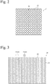
- Fig. 2 shows another example of arrangements of fine laser-beam-bored holes for forming the near-field electromagnetic wave absorbing film of the present invention.
- pluralities of laser-beam-bored holes 12 are arranged with substantially the same interval W in both vertical directions.
- the interval W is 50 ⁇ m or less, preferably 20 ⁇ m or less, more preferably 1-15 ⁇ m.
- Pluralities of openings as large as giving transmission viewability are partially formed in the bored thin metal film, to produce a near-field electromagnetic wave absorbing film.
- the shapes and arrangements of openings are not restrictive, as long as necessary transmission viewability is obtained while securing sufficient electromagnetic wave absorbability.
- the sizes of openings are also not restrictive, as long as necessary transmission viewability is obtained while securing sufficient electromagnetic wave absorbability, though they preferably have diameters of several millimeters to several tens of millimeters, for example, when they are circular as shown in Fig. 2 .
- the openings are preferably as large as 2-20 mm in diameter or width.
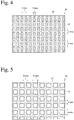
- Figs. 3-9 show examples of the shapes, sizes and arrangements of openings. Though the openings may be arranged in one direction, they are arranged preferably in at least two directions.
- pluralities of rectangular openings 21 are formed in parallel longitudinally and transversely in the bored thin metal film 1.
- Thin metal film portions remaining 22 after forming the rectangular openings 21, which may be called post-opening remaining portions, are in a lattice shape.
- pluralities of square openings 21 are formed in parallel longitudinally and transversely in the bored thin metal film 1.
- Thin metal film portions remaining 22 after forming the square openings 21, which may be called post-opening remaining portions, are in a lattice shape.
- pluralities of circular openings 21 are formed in parallel longitudinally and transversely in the bored thin metal film 1.
- Thin metal film portions remaining 22 after forming the circular openings 21, which may be called post-opening remaining portions, are in a lattice shape.
- pluralities of triangular openings 21 are formed in parallel longitudinally and transversely in the bored thin metal film 1.
- Thin metal film portions remaining 22 after forming the triangular openings 21, which may be called post-opening remaining portions, are in a deformed lattice shape.
- pluralities of rhombic openings 21 are formed in parallel longitudinally and transversely in the bored thin metal film 1.
- Thin metal film portions remaining 22 after forming the rhombic (inclined square) openings 21, which may be called post-opening remaining portions, are in a deformed lattice shape.
- the post-opening remaining portions 22 should be connected in at least one direction, preferably in at least two directions.
- the area ratio of openings 21 to the bored thin metal film 1 [100 x total area of openings 21/(total area of openings 21 + total area of post-opening remaining portions 22)] is preferably 15-60%, more preferably 20-50%.
- the area ratio of openings 21 is less than 15%, sufficient transmission viewability cannot be obtained.
- the area ratio of openings 21 is more than 60%, sufficient electromagnetic wave absorbability cannot be secured.
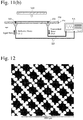
- the electric resistance of the bored thin metal film 1 is measured by a DC two-terminal method under pressure (simply called "under-pressure two-terminal method"), using an apparatus shown in Figs. 10(a) to 10(c) , to which a test piece TP1 of a composite film comprising a bored thin metal film 1 on a surface of a plastic film 10.
- a square test piece TP1 of 10 cm x 10 cm is placed with its bored thin metal film 1 above on a flat, hard insulation surface, a pair of electrodes 120, 120 each comprising an electrode body portion 121 of 10 cm in length, 1 cm in width and 0.5 mm in thickness, and an electrode extension 122 of 1 cm in width and 0.5 mm in thickness extending from a center side of the electrode body portion 121 are attached to opposing side portions of the square test piece TP1.
- a transparent acrylic plate 130 of 10 cm x 10 cm x 5 mm is placed on the test piece TP1 and both electrodes 120, 120, such that it completely covers them, and a cylindrical weight 140 (3.85 kg) of 10 cm in diameter is placed on the transparent acrylic plate 130, to measure current flowing between both electrode extensions 222, 222 to determine the electric resistance.
- the electric resistance measured under the above conditions is expressed by " ⁇ /100 cm 2 .”
- the bored thin metal film 1 should have electric resistance in a range of 50-300 ⁇ /100 cm 2 .
- the electric resistance is less than 50 ⁇ /100 cm 2 or more than 300 ⁇ /100 cm 2 , the near-field electromagnetic wave absorbing film 20 does not have sufficient electromagnetic wave absorbability.
- the electric resistance of the near-field electromagnetic wave absorbing film 20 is preferably 60-250 ⁇ /100 cm 2 , more preferably 80-200 ⁇ /100 cm 2 .
- a protective plastic layer (not shown) is preferably formed thereon.
- a plastic film for the protective plastic layer may be the same as the plastic film 10.
- the thickness of the protective plastic layer is preferably about 10-100 ⁇ m.
- a plastic film is preferably heat-laminated to the near-field electromagnetic wave absorbing film 20 as a protective layer.
- the heat lamination temperature may be 110-150°C.
- a plastic film for the protective layer is usually attached to the near-field electromagnetic wave absorbing film 20 after laser-beam-bored holes and openings are formed in the thin metal film 11 on the plastic film 10, the laser-beam-bored holes and the openings may be formed after the protective plastic film is attached to the thin metal film 11, as long as the protective plastic film is provided with a lot of fine pores in advance.
- the formation of fine pores in the protective plastic film can be conducted by the method described in Japanese Patent 2063411 .
- a system comprising a 50- ⁇ microstripline MSL (64.4 mm x 4.4 mm), an insulating substrate 220 supporting the microstripline MSL, a grounded electrode 221 attached to a lower surface of the insulating substrate 220, conductive pins 222, 222 connected to both ends of the microstripline MSL, a network analyzer NA, and coaxial cables 223, 223 connecting the network analyzer NA to the conductive pins 222, 222 as shown in Figs.
- Laser-beam-bored holes 12 of 200 ⁇ m or less in diameter are first formed with intervals of 50 ⁇ m or less on an entire surface of a thin metal film 11 formed on a plastic film 10 by, for example, vapor deposition.
- the bored thin metal film 1 is then partially provided with pluralities of openings 21 as large as giving transmission viewability.
- the openings 21 may be formed by irradiating laser beams.
- the laser-beam-bored holes 12 and the openings 21 can be formed by one irradiation operation of laser beams, the separate formation of laser-beam-bored holes 12 and openings 21 by two steps can produce the near-field electromagnetic wave absorbing film 20 with higher efficiency.
- the openings 21 may be formed by photolithography.
- the electric resistance of a square test piece TP1 (10 cm x 10 cm) cut out of each composite film was measured by the method described in Section [1] (4). The results are shown in Table 1. Table 1 No. Ref. Ex. 1 Com. Ex. 1 Com. Ex. 2 Corresponding Figure Fig. 12 Fig. 13 Fig.
- a test piece TP2 (55.2 mm x 4.7 mm) cut out of each composite film was adhered to a microstripline MSL in the system shown in Figs. 11(a) and 11(b) , to measure reflected wave power S 11 and transmitted wave power S 21 relative to input power P in in a frequency range of 0.1-6 GHz by the method described in Section [2], (1) and (2), thereby determining a transmission attenuation power ratio Rtp and a noise absorption ratio P loss /P in in a frequency range of 0.1-6 GHz.
- the S 11 , transmission attenuation power ratio Rtp and noise absorption ratio P loss /P in in a frequency range of 0.1-6 GHz are shown in Figs. 15, 16 and 17 , respectively.
- the intervals W of the laser-beam-bored holes 12 were about 20 ⁇ m.
- the electric resistance of each composite film measured by the same method as in Reference Example 1 was 60-80 ⁇ /100 cm 2 .
- the reflected wave power S 11 and transmitted wave power S 21 of the composite film in a frequency range of 0.1-6 GHz were measured in the same manner as in Reference Example 1, to determine the noise absorption ratio P loss /P in .
- the noise absorption ratio P loss /P in in a frequency range of 0.1-6 GHz is shown in Fig. 19 .
- the composite film of Reference Example 2 whose laser-beam-bored holes 12 and electric resistance met the requirements of the present invention, had a high noise absorption ratio P loss /P in .
- openings 21 shown in any one of Figs. 3-6 and 9 were formed in each composite film of Reference Examples 1 and 2, to produce a near-field electromagnetic wave absorbing film.
- the reflected wave power S 11 and transmitted wave power S 21 of a test piece TP2 of each near-field electromagnetic wave absorbing film to input power P in in a frequency range of 0.1-6 GHz were measured in the same manner as in Reference Example 1, to determine a transmission attenuation power ratio Rtp and a noise absorption ratio P loss /P in in a frequency range of 0.1-6 GHz.
- any near-field electromagnetic wave absorbing films of Examples 1-5 had small reflected wave power S 11 , and high transmission attenuation power ratios Rtp and noise absorption ratios P loss /P in . Also, the near-field electromagnetic wave absorbing films of Examples 1-5 had opening area ratios of 15-60%, providing good transmission viewability.
- the near-field electromagnetic wave absorbing film of the present invention has large numbers of fine laser-beam-bored holes formed on the entire surface, and pluralities of openings as large as giving transmission viewability, it has excellent electromagnetic wave absorbability as well as good transmission viewability.
- the near-field electromagnetic wave absorbing film of the present invention having such features is suitable for electronic appliances having so-called skeleton structures whose inside can be viewed, such as cell phones, smartphones, robots, game machines, etc.
Landscapes
- Engineering & Computer Science (AREA)
- Physics & Mathematics (AREA)
- Microelectronics & Electronic Packaging (AREA)
- Electromagnetism (AREA)
- Plasma & Fusion (AREA)
- Shielding Devices Or Components To Electric Or Magnetic Fields (AREA)
- Laminated Bodies (AREA)
Abstract
the thin metal film having laser-beam-bored holes of 200 µm or less in diameter with intervals of 50 µm or less on the entire surface, and pluralities of openings as large as giving transmission viewability partially on the surface.
Description
- The present invention relates to a near-field electromagnetic wave absorbing film having excellent electromagnetic wave absorbability and transmission viewability.
- Electromagnetic wave absorbing sheets for preventing the leak and intrusion of electromagnetic waves are used in communications equipments such as cell phones, smartphones, wireless LANs, etc., and electronic appliances such as computers, etc. Electromagnetic wave absorbing sheets widely used at present are formed by metal sheets or nets, and electromagnetic wave absorbing sheets comprising vapor-deposited metal films formed on plastic sheets are recently proposed. For example,
JP 9-148782 A -
WO 2010/093027 discloses a composite film comprising a single- or multi-layer, thin metal film formed on at least one surface of a plastic film, the thin metal film being provided with large numbers of substantially parallel, intermittent linear scratches with irregular widths and intervals in plural directions, thereby having reduced anisotropy of electromagnetic wave absorbability. - In the electromagnetic wave absorbing sheet of
JP 9-148782 A WO 2010/093027 having a linear-scratched thin metal film, the electromagnetic wave absorbability is obtained by linear pattern or linear scratches. However, it is also desired to efficiently obtain an electromagnetic wave absorbing film having excellent electromagnetic wave absorbability by forming laser-beam-bored holes in a pattern. - Further, due to the demand of transparent electromagnetic wave absorbing films, electromagnetic wave absorbing films having thin ITO films or thin CNT films are proposed, and used for ETCs, etc. However, electromagnetic wave absorbing films used for ETCs are far-field electromagnetic wave absorbing films, which are not used as near-field electromagnetic wave absorbing films because of difficulty in impedance control for near-field electromagnetic waves. Thus desired is a near-field electromagnetic wave absorbing film comprising an opaque layer having electromagnetic wave absorbability, through which items can be viewed. Such characteristic is called "transmission viewability."
- Accordingly, an object of the present invention is to provide a near-field electromagnetic wave absorbing film having excellent electromagnetic wave absorbability and transmission viewability.
- As a result of intensive research in view of the above object, the inventor has found that with (a) laser-beam-bored holes of 200 µm or less in diameter formed with intervals of 50 µm or less, and (b) pluralities of openings as large as giving transmission viewability formed partially, on an entire surface of a thin metal film on a plastic film, a near-field electromagnetic wave absorbing film having excellent electromagnetic wave absorbability and transmission viewability can be obtained. The present invention has been completed based on such finding.
- Thus, the near-field electromagnetic wave absorbing film of the present invention comprises a plastic film, and a single- or multi-layer, thin metal film formed on at least one surface of the plastic film;
the thin metal film having laser-beam-bored holes of 200 µm or less in diameter with intervals of 50 µm or less on the entire surface, and pluralities of openings as large as giving transmission viewability partially on the surface. - The diameters of the laser-beam-bored holes are preferably 100 µm or less, more preferably 20-100 µm.
- The laser-beam-bored holes are arranged preferably with intervals of 20 µm or less.
- The openings formed in the thin metal film are arranged preferably in at least two directions.
- The area ratio of the openings in the thin metal film is preferably 15-60%.
- The thickness of the thin metal film is preferably 10-300 nm.
- The thin metal film is preferably at least one metal selected from the group consisting of aluminum, copper, silver, tin, nickel, cobalt, chromium and their alloys.
-
-
Fig. 1(a) is a partial, enlarged plan view showing an example of arrangements of fine laser-beam-bored holes for forming the near-field electromagnetic wave absorbing film of the present invention. -
Fig. 1(b) is a cross-sectional view taken along the line A-A inFig. 1 . -
Fig. 1(c) is a partial, enlarged view ofFig. 1 . -
Fig. 2 is a partial, enlarged plan view showing another example of arrangements of fine laser-beam-bored holes for forming the near-field electromagnetic wave absorbing film of the present invention. -
Fig. 3 is a plan view showing an example of arrangements of openings for forming the near-field electromagnetic wave absorbing film of the present invention. -
Fig. 4 is a plan view showing another example of arrangements of openings for forming the near-field electromagnetic wave absorbing film of the present invention. -
Fig. 5 is a plan view showing a further example of arrangements of openings for forming the near-field electromagnetic wave absorbing film of the present invention. -
Fig. 6 is a plan view showing a still further example of arrangements of openings for forming the near-field electromagnetic wave absorbing film of the present invention. -
Fig. 7 is a plan view showing a still further example of arrangements of openings for forming the near-field electromagnetic wave absorbing film of the present invention. -
Fig. 8 is a plan view showing a still further example of arrangements of openings for forming the near-field electromagnetic wave absorbing film of the present invention. -
Fig. 9 is a plan view showing a still further example of arrangements of openings for forming the near-field electromagnetic wave absorbing film of the present invention. -
Fig. 10(a) is a perspective view showing an apparatus for measuring the electric resistance of a near-field electromagnetic wave absorbing film. -
Fig. 10(b) is a plan view showing the measurement of the electric resistance of a near-field electromagnetic wave absorbing film by the apparatus ofFig. 10(a) . -
Fig. 10(c) is a cross-sectional view taken along the line B-B inFig. 10(b) . -
Fig. 11(a) is a plan view showing a system for evaluating the electromagnetic wave absorbability of a near-field electromagnetic wave absorbing film. -
Fig. 11(b) is a partially cross-sectional front view showing a system for evaluating the electromagnetic wave absorbability of a near-field electromagnetic wave absorbing film. -
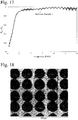
Fig. 12 is a photomicrograph showing the bored composite film of Reference Example 1. -
Fig. 13 is a photomicrograph showing the bored composite film of Comparative Example 1. -
Fig. 14 is a photomicrograph showing the bored composite film of Comparative Example 2. -
Fig. 15 is a graph showing the relations between S11 and the frequency of incident electromagnetic waves in the bored composite films of Reference Example 1 and Comparative Examples 1 and 2. -
Fig. 16 is a graph showing the relations between transmission attenuation power ratio Rtp and the frequency of incident electromagnetic waves in the bored composite films of Reference Example 1 and Comparative Examples 1 and 2. -
Fig. 17 is a graph showing the Ploss/Pin of the near-field electromagnetic wave absorbing film of Reference Example 1 at 0.1-6 GHz. -
Fig. 18 is a photomicrograph showing the bored composite film of Reference Example 2. -
Fig. 19 is a graph showing the Ploss/Pin of the bored composite film of Reference Example 2 at 0.1-6 GHz. -
Fig. 20 is a graph showing the S11, S21 and Rtp of the near-field electromagnetic wave absorbing film of Example 1 at 0.1-6 GHz. -
Fig. 21 is a graph showing the Ploss/Pin of the near-field electromagnetic wave absorbing film of Example 1 at 0.1-6 GHz. -
Fig. 22 is a graph showing the S11, S21 and Rtp of the near-field electromagnetic wave absorbing film of Example 2 at 0.1-6 GHz. -
Fig. 23 is a graph showing the Ploss/Pin of the near-field electromagnetic wave absorbing film of Example 2 at 0.1-6 GHz. -
Fig. 24 is a graph showing the S11, S21 and Rtp of the near-field electromagnetic wave absorbing film of Example 3 at 0.1-6 GHz. -
Fig. 25 is a graph showing the Ploss/Pin of the near-field electromagnetic wave absorbing film of Example 3 at 0.1-6 GHz. -
Fig. 26 is a graph showing the S11, S21 and Rtp of the near-field electromagnetic wave absorbing film of Example 4 at 0.1-6 GHz. -
Fig. 27 is a graph showing the Ploss/Pin of the near-field electromagnetic wave absorbing film of Example 4 at 0.1-6 GHz. -
Fig. 28 is a graph showing the S11, S21 and Rtp of the near-field electromagnetic wave absorbing film of Example 5 at 0.1-6 GHz. -
Fig. 29 is a graph showing the Ploss/Pin of the near-field electromagnetic wave absorbing film of Example 5 at 0.1-6 GHz. - The embodiments of the present invention will be explained referring to the attached drawings, and it should be noted that explanation concerning one embodiment is applicable to other embodiments unless otherwise mentioned. Also, the following explanations are not restrictive, but various modifications may be made within the scope of the present invention.
-
Figs. 1(a) to 1(c) show an example of arrangements of fine laser-beam-bored holes for forming the near-field electromagnetic wave absorbing film of the present invention. A thin metal film provided with large numbers of fine laser-beam-bored holes is hereinafter called "bored thin metal film." This boredthin metal film 1 is obtained by formingholes 12 in two crossing lines by laser beams in the single- or multi-layer,thin metal film 11 formed on a surface of theplastic film 10. - Resins forming the
plastic film 10 are not particularly restrictive as long as they have sufficient strength, flexibility and workability in addition to insulation, and they may be, for instance, polyesters (polyethylene terephthalate, etc.), polyarylene sulfide (polyphenylene sulfide, etc.), polyamides, polyimides, polyamideimides, polyether sulfone, polyetheretherketone, polycarbonates, acrylic resins, polystyrenes, polyolefins (polyethylene, polypropylene, etc.), etc. From the aspect of strength and cost, polyethylene terephthalate (PET) is preferable. The thickness of theplastic film 10 may be about 10-100 µm. - Metals forming the
thin metal film 11 are not particularly restrictive as long as they have conductivity, and they are preferably aluminum, copper, silver, tin, nickel, cobalt, chromium and their alloys, particularly aluminum, copper, nickel and their alloys, from the aspect of corrosion resistance and cost. The thickness of the thin metal film is preferably 10-300 nm, more preferably 20-200 nm, most preferably 30-150 nm. Thethin metal film 11 can be formed by vapor deposition (physical vapor deposition such as vacuum vapor deposition, sputtering or ion plating, or chemical vapor deposition such as plasma CVD, thermal CVD or photo-CVD), plating, or foil bonding. - When the
thin metal film 11 is a single layer,thin metal film 11 is preferably made of aluminum or nickel from the aspect of conductivity, corrosion resistance and cost. When thethin metal film 11 is a composite layer, one layer may be formed by a non-magnetic metal, and the other layer may be formed by a magnetic metal. The non-magnetic metal may be aluminum, copper, silver, tin or their alloys, and the magnetic metal may be nickel, cobalt, chromium or their alloys. The thickness of the non-magnetic metal layer and the thickness of the magnetic metal layer are not restrictive as long as their total thickness is within the above range. - As shown in
Figs. 1(a) to 1(c) , each laser-beam-bored hole 12 is a substantially circular hole formed by evaporating a metal by the irradiation of a laser beam to thethin metal film 11, without opening theplastic film 10. The diameter D of each laser-beam-bored hole 12 is 200 µm or less. When the diameter D is more than 200 µm, the number of laser-beam-boredholes 12 formed in a unit area is too small, resulting in too large portions of thethin metal film 11 remaining between the laser-beam-boredholes 12, which act as a reflecting film, and thus failing to obtain sufficient electromagnetic wave absorbability. The diameter D of each laser-beam-bored hole 12 is preferably 100 µm or less, more preferably 20-100 µm. - In the depicted example, the laser-beam-bored
holes 12 are arranged in two crossing lines in thethin metal film 11. Thethin metal film 11 is partitioned to individual main remainingportions 13 by crossinglines holes 12 are arranged with at least partial intervals, interval portions of thethin metal film 11 remain as narrow bridge-like portions 14. Accordingly, thinmetal film portions 11a remaining after forming the laser-beam-boredholes 12, which are called "remaining thin metal film portions," consist of the main remainingportions 13 and the narrow bridge-like portions 14. - The laser-beam-bored
holes 12 are preferably arranged with intervals in bothlines thin metal film 1 does not have desired electric resistance. The intervals W of adjacent laser-beam-bored holes 12 (widths of bridge-like portions 14) are preferably 20 µm or less, more preferably 1-15 µm. Accordingly, the maximum width Wmax of bridge-like portions 14 is 50 µm, preferably 20 µm. The average width Wav of bridge-like portions 14 is 3-30 µm, preferably 5-20 µm. - Though laser beam spots per se are circular, regions of the
thin metal film 1 evaporated by laser beams are not completely circular, but tend to have slightly irregular contours due to interference between adjacent laser-beam-boredholes 12. For example, when there is no space between adjacent laser-beam-boredholes 12, both laser-beam-boredholes like portions 14 with small widths. This seems to be due to the fact that an evaporated metal is solidified between adjacent laser beam spots, resulting in narrow bridge-like portions 14. Thus, even with laser beam spots arranged with the same interval, laser-beam-boredholes 12 actually formed by the evaporation of thethin metal film 11 do not have the same interval, but the bridge-like portions 14 have different widths W within a range of 50 µm or less. Accordingly, the near-field electromagnetic wave absorbing film of the present invention has excellent electromagnetic wave absorbability in a wide range of frequency. - The
lines - The size of main remaining
portions 13 largely depends on the centerline distance T between adjacent laser-beam-boredholes lines portions 13 affects the electric resistance (thus, electromagnetic wave absorbability) of the near-field electromagneticwave absorbing film 20, the centerline distance T betweenadjacent lines adjacent lines -
Fig. 2 shows another example of arrangements of fine laser-beam-bored holes for forming the near-field electromagnetic wave absorbing film of the present invention. In this bored thin metal film 1', pluralities of laser-beam-boredholes 12 are arranged with substantially the same interval W in both vertical directions. As in the above example, the interval W is 50 µm or less, preferably 20 µm or less, more preferably 1-15 µm. - Pluralities of openings as large as giving transmission viewability are partially formed in the bored thin metal film, to produce a near-field electromagnetic wave absorbing film. The shapes and arrangements of openings are not restrictive, as long as necessary transmission viewability is obtained while securing sufficient electromagnetic wave absorbability. The sizes of openings are also not restrictive, as long as necessary transmission viewability is obtained while securing sufficient electromagnetic wave absorbability, though they preferably have diameters of several millimeters to several tens of millimeters, for example, when they are circular as shown in
Fig. 2 . In general, the openings are preferably as large as 2-20 mm in diameter or width.Figs. 3-9 show examples of the shapes, sizes and arrangements of openings. Though the openings may be arranged in one direction, they are arranged preferably in at least two directions. - In the near-field electromagnetic
wave absorbing film 20 shown inFig. 3 , pluralities of parallel slit-like openings 21 are formed in the boredthin metal film 1. Thin metal film portions remaining 22 after forming the slit-like openings 21, which may be called post-opening remaining portions, are in a ribbon shape. - In the near-field electromagnetic
wave absorbing film 20 shown inFig. 4 , pluralities ofrectangular openings 21 are formed in parallel longitudinally and transversely in the boredthin metal film 1. Thin metal film portions remaining 22 after forming therectangular openings 21, which may be called post-opening remaining portions, are in a lattice shape. - In the near-field electromagnetic
wave absorbing film 20 shown inFig. 5 , pluralities ofsquare openings 21 are formed in parallel longitudinally and transversely in the boredthin metal film 1. Thin metal film portions remaining 22 after forming thesquare openings 21, which may be called post-opening remaining portions, are in a lattice shape. - In the near-field electromagnetic
wave absorbing film 20 shown inFig. 6 , pluralities ofcircular openings 21 are formed in parallel longitudinally and transversely in the boredthin metal film 1. Thin metal film portions remaining 22 after forming thecircular openings 21, which may be called post-opening remaining portions, are in a lattice shape. - In the near-field electromagnetic
wave absorbing film 20 shown inFig. 7 , pluralities oftriangular openings 21 are formed in parallel longitudinally and transversely in the boredthin metal film 1. Thin metal film portions remaining 22 after forming thetriangular openings 21, which may be called post-opening remaining portions, are in a deformed lattice shape. - In the near-field electromagnetic
wave absorbing film 20 shown inFig. 8 , pluralities ofrhombic openings 21 are formed in parallel longitudinally and transversely in the boredthin metal film 1. Thin metal film portions remaining 22 after forming the rhombic (inclined square)openings 21, which may be called post-opening remaining portions, are in a deformed lattice shape. - In the near-field electromagnetic
wave absorbing film 20 shown inFig. 9 , plural pairs oftriangular openings 21 are formed in parallel longitudinally and transversely in the boredthin metal film 1. Thin metal film portions remaining 22 after forming thetriangular openings 21, which may be called post-opening remaining portions, are in a deformed lattice shape. - As shown in
Figs. 3-9 , thepost-opening remaining portions 22 should be connected in at least one direction, preferably in at least two directions. The area ratio ofopenings 21 to the bored thin metal film 1 [100 x total area ofopenings 21/(total area ofopenings 21 + total area of post-opening remaining portions 22)] is preferably 15-60%, more preferably 20-50%. When the area ratio ofopenings 21 is less than 15%, sufficient transmission viewability cannot be obtained. On the other hand, when the area ratio ofopenings 21 is more than 60%, sufficient electromagnetic wave absorbability cannot be secured. - The electromagnetic wave absorbability of the near-field electromagnetic
wave absorbing film 20 basically depends on the electromagnetic wave absorbability of the boredthin metal film 1. Intensive research has revealed that the electromagnetic wave absorbability of the boredthin metal film 1 depends on the sizes and electric resistance of bored thinmetal film portions 11a remaining after forming the laser-beam-bored holes 12 (remaining bored thinmetal film portions 11a = bored main remainingportions 13 + bored bridge-like portions 14). The boredthin metal film 1 having electric resistance of 50-300 Ω/100 cm2 has excellent electromagnetic wave absorbability in a wide range of frequency. - The electric resistance of the bored
thin metal film 1 is measured by a DC two-terminal method under pressure (simply called "under-pressure two-terminal method"), using an apparatus shown inFigs. 10(a) to 10(c) , to which a test piece TP1 of a composite film comprising a boredthin metal film 1 on a surface of aplastic film 10. Specifically, a square test piece TP1 of 10 cm x 10 cm is placed with its boredthin metal film 1 above on a flat, hard insulation surface, a pair ofelectrodes electrode body portion 121 of 10 cm in length, 1 cm in width and 0.5 mm in thickness, and anelectrode extension 122 of 1 cm in width and 0.5 mm in thickness extending from a center side of theelectrode body portion 121 are attached to opposing side portions of the square test piece TP1. A transparentacrylic plate 130 of 10 cm x 10 cm x 5 mm is placed on the test piece TP1 and bothelectrodes acrylic plate 130, to measure current flowing between bothelectrode extensions - The bored thin metal film 1 (near-field electromagnetic wave absorbing film 20) should have electric resistance in a range of 50-300 Ω/100 cm2. When the electric resistance is less than 50 Ω/100 cm2 or more than 300 Ω/100 cm2, the near-field electromagnetic
wave absorbing film 20 does not have sufficient electromagnetic wave absorbability. The electric resistance of the near-field electromagneticwave absorbing film 20 is preferably 60-250 Ω/100 cm2, more preferably 80-200 Ω/100 cm2. - To protect the bored
thin metal film 1, a protective plastic layer (not shown) is preferably formed thereon. A plastic film for the protective plastic layer may be the same as theplastic film 10. The thickness of the protective plastic layer is preferably about 10-100 µm. To prevent detachment, a plastic film is preferably heat-laminated to the near-field electromagneticwave absorbing film 20 as a protective layer. When the protective plastic layer is formed by a PET film, the heat lamination temperature may be 110-150°C. - Though a plastic film for the protective layer is usually attached to the near-field electromagnetic
wave absorbing film 20 after laser-beam-bored holes and openings are formed in thethin metal film 11 on theplastic film 10, the laser-beam-bored holes and the openings may be formed after the protective plastic film is attached to thethin metal film 11, as long as the protective plastic film is provided with a lot of fine pores in advance. The formation of fine pores in the protective plastic film can be conducted by the method described inJapanese Patent 2063411 - Using a system comprising a 50-Ω microstripline MSL (64.4 mm x 4.4 mm), an insulating
substrate 220 supporting the microstripline MSL, a groundedelectrode 221 attached to a lower surface of the insulatingsubstrate 220,conductive pins coaxial cables conductive pins Figs. 11(a) and11(b) , a test piece TP2 of each near-field electromagneticwave absorbing film 20 is adhered to the microstripline MSL to measure its reflected wave power S11 and transmitted wave power S21 to an input electromagnetic wave of 0.1-6 GHz, thereby determining its transmission attenuation power ratio Rtp by the following formula (1):
- In the system shown in
Figs. 11(a) and11(b) , input power Pin = reflected wave power S11 + transmitted wave power S21 + absorbed power (power loss) Ploss. Accordingly, the noise absorption ratio Ploss/Pin is determined by subtracting the reflected wave power S11 and the transmitted wave power S21 from the input power Pin, and dividing the resultant power loss Ploss by the input power Pin. - Laser-beam-bored
holes 12 of 200 µm or less in diameter are first formed with intervals of 50 µm or less on an entire surface of athin metal film 11 formed on aplastic film 10 by, for example, vapor deposition. The boredthin metal film 1 is then partially provided with pluralities ofopenings 21 as large as giving transmission viewability. Theopenings 21 may be formed by irradiating laser beams. In this case, though the laser-beam-boredholes 12 and theopenings 21 can be formed by one irradiation operation of laser beams, the separate formation of laser-beam-boredholes 12 andopenings 21 by two steps can produce the near-field electromagneticwave absorbing film 20 with higher efficiency. Incidentally, theopenings 21 may be formed by photolithography. - The present invention will be explained in more detail referring to Examples below without intention of restriction.
- A
thin Ni film 11 as thick as 50 nm, which was vacuum-vapor-deposited on eachPET film 10 as thick as 16 µm, was provided with laser-beam-boredholes 12 of 60 µm in diameter in two crossing lines by a 3-Axis hybrid laser marker (MD-X1000 available from Keyence Corporation), to produce a composite film having a boredthin Ni film 1 shown inFigs. 12-14 . The electric resistance of a square test piece TP1 (10 cm x 10 cm) cut out of each composite film was measured by the method described in Section [1] (4). The results are shown in Table 1.Table 1 No. Ref. Ex. 1 Com. Ex. 1 Com. Ex. 2 Corresponding Figure Fig. 12 Fig. 13 Fig. 14 Crossing Angle θ(1) (°) 90 90 90 Maximum Width Wmax (µm) 15 60 0 Average Width Wav (µm) 7 50 0 Electric Resistance (Ω/100 cm2) 60 6 ∞ Note: (1) The crossing angle θ of two lines of laser-beam-bored holes. - A test piece TP2 (55.2 mm x 4.7 mm) cut out of each composite film was adhered to a microstripline MSL in the system shown in
Figs. 11(a) and11(b) , to measure reflected wave power S11 and transmitted wave power S21 relative to input power Pin in a frequency range of 0.1-6 GHz by the method described in Section [2], (1) and (2), thereby determining a transmission attenuation power ratio Rtp and a noise absorption ratio Ploss/Pin in a frequency range of 0.1-6 GHz. The S11, transmission attenuation power ratio Rtp and noise absorption ratio Ploss/Pin in a frequency range of 0.1-6 GHz are shown inFigs. 15, 16 and17 , respectively. As is clear fromFig. 15 , there was a large reflected wave power S11 in Comparative Example 1 having too few laser-beam-bored holes 12 (too low electric resistance). Also, as is clear fromFig. 16 , there was a low transmission attenuation power ratio Rtp in Comparative Example 2 having excessive laser-beam-bored holes 12 (too high electric resistance). Further, as is clear fromFig. 17 , the composite film of Reference Example 1 had an excellent noise absorption ratio Ploss/Pin. - A
thin A1 film 11 as thick as 80 nm, which was vacuum-vapor-deposited on eachPET film 10 as thick as 16 µm, was provided with laser-beam-boredholes 12 of 80 µm in diameter in two crossing lines by a 3-Axis hybrid laser marker (MD-X1000 available from Keyence Corporation), to produce a composite film having a boredthin A1 film 1 shown inFig. 18 . The intervals W of the laser-beam-boredholes 12 were about 20 µm. The electric resistance of each composite film measured by the same method as in Reference Example 1 was 60-80 Ω/100 cm2. - The reflected wave power S11 and transmitted wave power S21 of the composite film in a frequency range of 0.1-6 GHz were measured in the same manner as in Reference Example 1, to determine the noise absorption ratio Ploss/Pin. The noise absorption ratio Ploss/Pin in a frequency range of 0.1-6 GHz is shown in
Fig. 19 . As is clear fromFig. 19 , the composite film of Reference Example 2, whose laser-beam-boredholes 12 and electric resistance met the requirements of the present invention, had a high noise absorption ratio Ploss/Pin. - As shown in Table 2 below,
openings 21 shown in any one ofFigs. 3-6 and9 were formed in each composite film of Reference Examples 1 and 2, to produce a near-field electromagnetic wave absorbing film. The reflected wave power S11 and transmitted wave power S21 of a test piece TP2 of each near-field electromagnetic wave absorbing film to input power Pin in a frequency range of 0.1-6 GHz were measured in the same manner as in Reference Example 1, to determine a transmission attenuation power ratio Rtp and a noise absorption ratio Ploss/Pin in a frequency range of 0.1-6 GHz. With respect to Examples 1-5,Figs. 20 ,22 ,24 ,26 and28 show S11, S21 and Rtp in a frequency range of 0.1-6 GHz, andFigs. 21 ,23 ,25 ,27 and29 show Ploss/Pin in a frequency range of 0.1-6 GHz.Table 2 No. Example 1 Example 2 Example 3 Example 4 Example 5 Thin Metal Film Metal (Thickness: nm) Ref. Ex. 1 Ni (50) Ref. Ex. 2 Al (80) Ref. Ex. 2 Al (80) Ref. Ex. 2 Al (80) Ref. Ex. 2 Al (80) Bored Thin Metal Film Fig. 12 Fig. 18 Fig. 18 Fig. 18 Fig. 18 Openings Fig. 3 Fig. 4 Fig. 5 Fig. 6 Fig. 9 Area Ratio of Openings (%) 33 24 36 40 44 - As is clear from
Figs. 20-29 , any near-field electromagnetic wave absorbing films of Examples 1-5 had small reflected wave power S11, and high transmission attenuation power ratios Rtp and noise absorption ratios Ploss/Pin. Also, the near-field electromagnetic wave absorbing films of Examples 1-5 had opening area ratios of 15-60%, providing good transmission viewability. - Because the near-field electromagnetic wave absorbing film of the present invention has large numbers of fine laser-beam-bored holes formed on the entire surface, and pluralities of openings as large as giving transmission viewability, it has excellent electromagnetic wave absorbability as well as good transmission viewability. The near-field electromagnetic wave absorbing film of the present invention having such features is suitable for electronic appliances having so-called skeleton structures whose inside can be viewed, such as cell phones, smartphones, robots, game machines, etc.
-
- 1: Bored thin metal film
- 10: Plastic film
- 11: Thin metal film
- 11 a: Remaining thin metal film portion
- 12: Laser-beam-bored hole
- 12a, 12b: Line of laser-beam-bored holes
- 13: Main remaining portion
- 14: Bridge-like portion
- 20: Near-field electromagnetic wave absorbing film
- 21: Opening
- 22: Post-opening remaining portion
- 120: Electrode
- 121: Electrode body portion
- 122: Electrode extension
- 130: Transparent acrylic plate
- 140: Cylindrical weight
- 220: Insulating substrate
- 221: Grounded electrode
- 222: Conductive pin
- 223: Coaxial cable
- D: Diameter of laser-beam-bored hole
- W: Width of bridge-like portion
- T: Centerline distance between adjacent laser-beam-bored holes lines
- TP1, TP2: Test piece of near-field electromagnetic wave absorbing film
- MSL: Microstripline
- NA: Network analyzer
Claims (8)
- A near-field electromagnetic wave absorbing film comprising a plastic film, and a single- or multi-layer, thin metal film formed on one surface of said plastic film;
said thin metal film having laser-beam-bored holes of 200 µm or less in diameter with intervals of 50 µm or less on the entire surface, and pluralities of openings as large as giving transmission viewability partially on the surface. - The near-field electromagnetic wave absorbing film according to claim 1, wherein said laser-beam-bored holes have diameters of 100 µm or less.
- The near-field electromagnetic wave absorbing film according to claim 2, wherein said laser-beam-bored holes have diameters of 20-100 µm.
- The near-field electromagnetic wave absorbing film according to any one of claims 1-3, wherein said laser-beam-bored holes are arranged with intervals of 20 µm or less.
- The near-field electromagnetic wave absorbing film according to any one of claims 1-4, wherein said openings formed in said thin metal film are arranged in at least two directions.
- The near-field electromagnetic wave absorbing film according to any one of claims 1-5, wherein the area ratio of said openings is 15-60%.
- The near-field electromagnetic wave absorbing film according to any one of claims 1-6, wherein the thickness of said thin metal film is 10-300 nm.
- The near-field electromagnetic wave absorbing film according to any one of claims 1-7, wherein said thin metal film is made of at least one metal selected from the group consisting of aluminum, copper, silver, tin, nickel, cobalt, chromium and their alloys.
Applications Claiming Priority (1)
| Application Number | Priority Date | Filing Date | Title |
|---|---|---|---|
| JP2016074369A JP6027281B1 (en) | 2016-04-01 | 2016-04-01 | Near-field electromagnetic wave absorbing film |
Publications (2)
| Publication Number | Publication Date |
|---|---|
| EP3226668A1 true EP3226668A1 (en) | 2017-10-04 |
| EP3226668B1 EP3226668B1 (en) | 2021-05-05 |
Family
ID=57326668
Family Applications (1)
| Application Number | Title | Priority Date | Filing Date |
|---|---|---|---|
| EP16200503.7A Active EP3226668B1 (en) | 2016-04-01 | 2016-11-24 | Near-field electromagnetic wave absorbing film |
Country Status (6)
| Country | Link |
|---|---|
| US (1) | US10056697B2 (en) |
| EP (1) | EP3226668B1 (en) |
| JP (1) | JP6027281B1 (en) |
| KR (1) | KR20170112991A (en) |
| CN (1) | CN107263936B (en) |
| TW (1) | TWI706713B (en) |
Families Citing this family (5)
| Publication number | Priority date | Publication date | Assignee | Title |
|---|---|---|---|---|
| DE102016101756A1 (en) * | 2016-02-01 | 2017-08-03 | Vega Grieshaber Kg | Method for determining and displaying the optimum material thickness in level measurement with radar sensors |
| JP6461414B1 (en) * | 2018-08-02 | 2019-01-30 | 加川 清二 | Electromagnetic wave absorbing composite sheet |
| US11281340B2 (en) * | 2019-01-18 | 2022-03-22 | Cirque Corporation | Radio frequency transparent capacitive touch systems and methods |
| JP7363103B2 (en) * | 2019-05-30 | 2023-10-18 | 東洋インキScホールディングス株式会社 | Electromagnetic shielding sheets and printed wiring boards |
| WO2023027305A1 (en) * | 2021-08-27 | 2023-03-02 | 삼성전자주식회사 | Exterior material for cooking device and preparation method therefor |
Citations (7)
| Publication number | Priority date | Publication date | Assignee | Title |
|---|---|---|---|---|
| JPH0263411A (en) | 1988-03-03 | 1990-03-02 | Salvarani Ind Spa | Module-type kitchen unit |
| JPH09148782A (en) | 1995-11-27 | 1997-06-06 | Nippon Paint Co Ltd | Transparent electromagnetic wave absorbing/shielding material |
| EP1993338A1 (en) * | 2006-03-09 | 2008-11-19 | Bridgestone Corporation | Process for producing translucent electromagnetic wave shielding material, translucent electromagnetic wave shielding material and display filter |
| WO2010093027A1 (en) | 2009-02-13 | 2010-08-19 | Kagawa Seiji | Metal thin film-plastic film composite film with linear streaks and apparatus for producing same |
| WO2011017037A2 (en) * | 2009-08-03 | 2011-02-10 | 3M Innovative Properties Company | Process for forming optically clear conductive metal or metal alloy thin films and films made therefrom |
| US20140224411A1 (en) * | 2011-05-12 | 2014-08-14 | Subtron Technology Co., Ltd. | Manufacturing method of cover structure |
| WO2014148589A1 (en) * | 2013-03-21 | 2014-09-25 | 株式会社ノリタケカンパニーリミテド | Electromagnetic shield |
Family Cites Families (9)
| Publication number | Priority date | Publication date | Assignee | Title |
|---|---|---|---|---|
| US5855988A (en) | 1995-11-27 | 1999-01-05 | Nippon Paint Co., Ltd. | Electromagnetic wave absorbing shielding material |
| JP2002313140A (en) * | 2001-04-13 | 2002-10-25 | Mitsui Chemicals Inc | Transparent conductive film, optical filter and its manufacturing method |
| JP2002317280A (en) * | 2001-04-18 | 2002-10-31 | Toyo Metallizing Co Ltd | Metallized plastic film |
| KR100939747B1 (en) * | 2001-05-16 | 2010-02-04 | 가부시키가이샤 브리지스톤 | Electromagnetic wave shielding light-transmitting window member, its manufacturing method, and display panel |
| KR20090108781A (en) * | 2008-04-14 | 2009-10-19 | 주식회사 동진쎄미켐 | Black paste composition having conductivity property, filter for shielding electromagnetic interference and display device comprising the same |
| JP2011142198A (en) * | 2010-01-07 | 2011-07-21 | Mitsubishi Rayon Co Ltd | Radiowave absorber |
| JP5069365B1 (en) * | 2011-06-30 | 2012-11-07 | 清二 加川 | Near-field noise suppression film |
| CN103959927B (en) * | 2011-11-30 | 2017-07-18 | 加川清二 | Composite electromagnetic absorbing sheet |
| WO2014126394A1 (en) * | 2013-02-15 | 2014-08-21 | 주식회사 아모텍 | Electromagnetic wave absorbing sheet and antenna module having same |
-
2016
- 2016-04-01 JP JP2016074369A patent/JP6027281B1/en active Active
- 2016-11-24 EP EP16200503.7A patent/EP3226668B1/en active Active
- 2016-11-28 TW TW105139019A patent/TWI706713B/en active
- 2016-11-29 US US15/363,793 patent/US10056697B2/en active Active
- 2016-12-29 KR KR1020160182492A patent/KR20170112991A/en active IP Right Grant
-
2017
- 2017-01-18 CN CN201710040228.7A patent/CN107263936B/en active Active
Patent Citations (8)
| Publication number | Priority date | Publication date | Assignee | Title |
|---|---|---|---|---|
| JPH0263411A (en) | 1988-03-03 | 1990-03-02 | Salvarani Ind Spa | Module-type kitchen unit |
| JPH09148782A (en) | 1995-11-27 | 1997-06-06 | Nippon Paint Co Ltd | Transparent electromagnetic wave absorbing/shielding material |
| EP1993338A1 (en) * | 2006-03-09 | 2008-11-19 | Bridgestone Corporation | Process for producing translucent electromagnetic wave shielding material, translucent electromagnetic wave shielding material and display filter |
| WO2010093027A1 (en) | 2009-02-13 | 2010-08-19 | Kagawa Seiji | Metal thin film-plastic film composite film with linear streaks and apparatus for producing same |
| WO2011017037A2 (en) * | 2009-08-03 | 2011-02-10 | 3M Innovative Properties Company | Process for forming optically clear conductive metal or metal alloy thin films and films made therefrom |
| US20140224411A1 (en) * | 2011-05-12 | 2014-08-14 | Subtron Technology Co., Ltd. | Manufacturing method of cover structure |
| WO2014148589A1 (en) * | 2013-03-21 | 2014-09-25 | 株式会社ノリタケカンパニーリミテド | Electromagnetic shield |
| US20160289816A1 (en) * | 2013-03-21 | 2016-10-06 | Noritake Co., Limited | Electromagnetic shield |
Also Published As
| Publication number | Publication date |
|---|---|
| US20170288314A1 (en) | 2017-10-05 |
| TWI706713B (en) | 2020-10-01 |
| CN107263936B (en) | 2021-04-09 |
| TW201811157A (en) | 2018-03-16 |
| KR20170112991A (en) | 2017-10-12 |
| JP2017188506A (en) | 2017-10-12 |
| EP3226668B1 (en) | 2021-05-05 |
| US10056697B2 (en) | 2018-08-21 |
| CN107263936A (en) | 2017-10-20 |
| JP6027281B1 (en) | 2016-11-16 |
Similar Documents
| Publication | Publication Date | Title |
|---|---|---|
| EP3226668A1 (en) | Near-field electromagnetic wave absorbing film | |
| JP4685977B2 (en) | Metal film with thin line-plastic composite film and manufacturing apparatus thereof | |
| TWI613955B (en) | Composite electromagnetic wave absorbing sheet | |
| KR101953599B1 (en) | Electromagnetic wave absorption film having high heat dissipation properties | |
| US9326433B2 (en) | Composite electromagnetic-wave-absorbing film | |
| TWI569713B (en) | Near-field electromagnetic wave absorber | |
| EP3735119A1 (en) | Electromagnetic wave absorbing body, article with electromagnetic wave absorbing body, and electromagnetic wave absorbing body manufacturing method | |
| TW201901703A (en) | Electromagnetic wave absorption filter | |
| US20240061474A1 (en) | Near-field electromagnetic wave absorber | |
| JP2013084864A (en) | Electromagnetic wave absorption flexible circuit board and electromagnetic wave absorption flexible substrate sheet used in the same | |
| KR102168863B1 (en) | Electromagnetic-wave-absorbing composite sheet | |
| JP5107394B2 (en) | Electromagnetic wave absorber and interior material using the same | |
| EP3211982B1 (en) | Near-field electromagnetic wave absorbing film | |
| JP2011258715A (en) | Transparent electromagnetic wave absorption film |
Legal Events
| Date | Code | Title | Description |
|---|---|---|---|
| PUAI | Public reference made under article 153(3) epc to a published international application that has entered the european phase |
Free format text: ORIGINAL CODE: 0009012 |
|
| STAA | Information on the status of an ep patent application or granted ep patent |
Free format text: STATUS: THE APPLICATION HAS BEEN PUBLISHED |
|
| AK | Designated contracting states |
Kind code of ref document: A1 Designated state(s): AL AT BE BG CH CY CZ DE DK EE ES FI FR GB GR HR HU IE IS IT LI LT LU LV MC MK MT NL NO PL PT RO RS SE SI SK SM TR |
|
| AX | Request for extension of the european patent |
Extension state: BA ME |
|
| STAA | Information on the status of an ep patent application or granted ep patent |
Free format text: STATUS: REQUEST FOR EXAMINATION WAS MADE |
|
| 17P | Request for examination filed |
Effective date: 20180320 |
|
| RBV | Designated contracting states (corrected) |
Designated state(s): AL AT BE BG CH CY CZ DE DK EE ES FI FR GB GR HR HU IE IS IT LI LT LU LV MC MK MT NL NO PL PT RO RS SE SI SK SM TR |
|
| GRAP | Despatch of communication of intention to grant a patent |
Free format text: ORIGINAL CODE: EPIDOSNIGR1 |
|
| STAA | Information on the status of an ep patent application or granted ep patent |
Free format text: STATUS: GRANT OF PATENT IS INTENDED |
|
| INTG | Intention to grant announced |
Effective date: 20201221 |
|
| GRAS | Grant fee paid |
Free format text: ORIGINAL CODE: EPIDOSNIGR3 |
|
| GRAA | (expected) grant |
Free format text: ORIGINAL CODE: 0009210 |
|
| STAA | Information on the status of an ep patent application or granted ep patent |
Free format text: STATUS: THE PATENT HAS BEEN GRANTED |
|
| AK | Designated contracting states |
Kind code of ref document: B1 Designated state(s): AL AT BE BG CH CY CZ DE DK EE ES FI FR GB GR HR HU IE IS IT LI LT LU LV MC MK MT NL NO PL PT RO RS SE SI SK SM TR |
|
| REG | Reference to a national code |
Ref country code: GB Ref legal event code: FG4D |
|
| REG | Reference to a national code |
Ref country code: CH Ref legal event code: EP |
|
| REG | Reference to a national code |
Ref country code: AT Ref legal event code: REF Ref document number: 1391525 Country of ref document: AT Kind code of ref document: T Effective date: 20210515 |
|
| REG | Reference to a national code |
Ref country code: IE Ref legal event code: FG4D |
|
| REG | Reference to a national code |
Ref country code: DE Ref legal event code: R096 Ref document number: 602016057278 Country of ref document: DE |
|
| REG | Reference to a national code |
Ref country code: LT Ref legal event code: MG9D |
|
| REG | Reference to a national code |
Ref country code: AT Ref legal event code: MK05 Ref document number: 1391525 Country of ref document: AT Kind code of ref document: T Effective date: 20210505 |
|
| PG25 | Lapsed in a contracting state [announced via postgrant information from national office to epo] |
Ref country code: FI Free format text: LAPSE BECAUSE OF FAILURE TO SUBMIT A TRANSLATION OF THE DESCRIPTION OR TO PAY THE FEE WITHIN THE PRESCRIBED TIME-LIMIT Effective date: 20210505 Ref country code: LT Free format text: LAPSE BECAUSE OF FAILURE TO SUBMIT A TRANSLATION OF THE DESCRIPTION OR TO PAY THE FEE WITHIN THE PRESCRIBED TIME-LIMIT Effective date: 20210505 Ref country code: AT Free format text: LAPSE BECAUSE OF FAILURE TO SUBMIT A TRANSLATION OF THE DESCRIPTION OR TO PAY THE FEE WITHIN THE PRESCRIBED TIME-LIMIT Effective date: 20210505 Ref country code: BG Free format text: LAPSE BECAUSE OF FAILURE TO SUBMIT A TRANSLATION OF THE DESCRIPTION OR TO PAY THE FEE WITHIN THE PRESCRIBED TIME-LIMIT Effective date: 20210805 Ref country code: HR Free format text: LAPSE BECAUSE OF FAILURE TO SUBMIT A TRANSLATION OF THE DESCRIPTION OR TO PAY THE FEE WITHIN THE PRESCRIBED TIME-LIMIT Effective date: 20210505 |
|
| PG25 | Lapsed in a contracting state [announced via postgrant information from national office to epo] |
Ref country code: SE Free format text: LAPSE BECAUSE OF FAILURE TO SUBMIT A TRANSLATION OF THE DESCRIPTION OR TO PAY THE FEE WITHIN THE PRESCRIBED TIME-LIMIT Effective date: 20210505 Ref country code: RS Free format text: LAPSE BECAUSE OF FAILURE TO SUBMIT A TRANSLATION OF THE DESCRIPTION OR TO PAY THE FEE WITHIN THE PRESCRIBED TIME-LIMIT Effective date: 20210505 Ref country code: PL Free format text: LAPSE BECAUSE OF FAILURE TO SUBMIT A TRANSLATION OF THE DESCRIPTION OR TO PAY THE FEE WITHIN THE PRESCRIBED TIME-LIMIT Effective date: 20210505 Ref country code: PT Free format text: LAPSE BECAUSE OF FAILURE TO SUBMIT A TRANSLATION OF THE DESCRIPTION OR TO PAY THE FEE WITHIN THE PRESCRIBED TIME-LIMIT Effective date: 20210906 Ref country code: NO Free format text: LAPSE BECAUSE OF FAILURE TO SUBMIT A TRANSLATION OF THE DESCRIPTION OR TO PAY THE FEE WITHIN THE PRESCRIBED TIME-LIMIT Effective date: 20210805 Ref country code: IS Free format text: LAPSE BECAUSE OF FAILURE TO SUBMIT A TRANSLATION OF THE DESCRIPTION OR TO PAY THE FEE WITHIN THE PRESCRIBED TIME-LIMIT Effective date: 20210905 Ref country code: GR Free format text: LAPSE BECAUSE OF FAILURE TO SUBMIT A TRANSLATION OF THE DESCRIPTION OR TO PAY THE FEE WITHIN THE PRESCRIBED TIME-LIMIT Effective date: 20210806 Ref country code: LV Free format text: LAPSE BECAUSE OF FAILURE TO SUBMIT A TRANSLATION OF THE DESCRIPTION OR TO PAY THE FEE WITHIN THE PRESCRIBED TIME-LIMIT Effective date: 20210505 |
|
| REG | Reference to a national code |
Ref country code: NL Ref legal event code: MP Effective date: 20210505 |
|
| PG25 | Lapsed in a contracting state [announced via postgrant information from national office to epo] |
Ref country code: NL Free format text: LAPSE BECAUSE OF FAILURE TO SUBMIT A TRANSLATION OF THE DESCRIPTION OR TO PAY THE FEE WITHIN THE PRESCRIBED TIME-LIMIT Effective date: 20210505 |
|
| PG25 | Lapsed in a contracting state [announced via postgrant information from national office to epo] |
Ref country code: RO Free format text: LAPSE BECAUSE OF FAILURE TO SUBMIT A TRANSLATION OF THE DESCRIPTION OR TO PAY THE FEE WITHIN THE PRESCRIBED TIME-LIMIT Effective date: 20210505 Ref country code: ES Free format text: LAPSE BECAUSE OF FAILURE TO SUBMIT A TRANSLATION OF THE DESCRIPTION OR TO PAY THE FEE WITHIN THE PRESCRIBED TIME-LIMIT Effective date: 20210505 Ref country code: CZ Free format text: LAPSE BECAUSE OF FAILURE TO SUBMIT A TRANSLATION OF THE DESCRIPTION OR TO PAY THE FEE WITHIN THE PRESCRIBED TIME-LIMIT Effective date: 20210505 Ref country code: EE Free format text: LAPSE BECAUSE OF FAILURE TO SUBMIT A TRANSLATION OF THE DESCRIPTION OR TO PAY THE FEE WITHIN THE PRESCRIBED TIME-LIMIT Effective date: 20210505 Ref country code: DK Free format text: LAPSE BECAUSE OF FAILURE TO SUBMIT A TRANSLATION OF THE DESCRIPTION OR TO PAY THE FEE WITHIN THE PRESCRIBED TIME-LIMIT Effective date: 20210505 Ref country code: SK Free format text: LAPSE BECAUSE OF FAILURE TO SUBMIT A TRANSLATION OF THE DESCRIPTION OR TO PAY THE FEE WITHIN THE PRESCRIBED TIME-LIMIT Effective date: 20210505 Ref country code: SM Free format text: LAPSE BECAUSE OF FAILURE TO SUBMIT A TRANSLATION OF THE DESCRIPTION OR TO PAY THE FEE WITHIN THE PRESCRIBED TIME-LIMIT Effective date: 20210505 |
|
| REG | Reference to a national code |
Ref country code: DE Ref legal event code: R097 Ref document number: 602016057278 Country of ref document: DE |
|
| PLBE | No opposition filed within time limit |
Free format text: ORIGINAL CODE: 0009261 |
|
| STAA | Information on the status of an ep patent application or granted ep patent |
Free format text: STATUS: NO OPPOSITION FILED WITHIN TIME LIMIT |
|
| 26N | No opposition filed |
Effective date: 20220208 |
|
| PG25 | Lapsed in a contracting state [announced via postgrant information from national office to epo] |
Ref country code: IS Free format text: LAPSE BECAUSE OF FAILURE TO SUBMIT A TRANSLATION OF THE DESCRIPTION OR TO PAY THE FEE WITHIN THE PRESCRIBED TIME-LIMIT Effective date: 20210905 Ref country code: AL Free format text: LAPSE BECAUSE OF FAILURE TO SUBMIT A TRANSLATION OF THE DESCRIPTION OR TO PAY THE FEE WITHIN THE PRESCRIBED TIME-LIMIT Effective date: 20210505 |
|
| REG | Reference to a national code |
Ref country code: DE Ref legal event code: R119 Ref document number: 602016057278 Country of ref document: DE |
|
| PG25 | Lapsed in a contracting state [announced via postgrant information from national office to epo] |
Ref country code: MC Free format text: LAPSE BECAUSE OF FAILURE TO SUBMIT A TRANSLATION OF THE DESCRIPTION OR TO PAY THE FEE WITHIN THE PRESCRIBED TIME-LIMIT Effective date: 20210505 |
|
| REG | Reference to a national code |
Ref country code: CH Ref legal event code: PL |
|
| GBPC | Gb: european patent ceased through non-payment of renewal fee |
Effective date: 20211124 |
|
| PG25 | Lapsed in a contracting state [announced via postgrant information from national office to epo] |
Ref country code: LU Free format text: LAPSE BECAUSE OF NON-PAYMENT OF DUE FEES Effective date: 20211124 Ref country code: IT Free format text: LAPSE BECAUSE OF FAILURE TO SUBMIT A TRANSLATION OF THE DESCRIPTION OR TO PAY THE FEE WITHIN THE PRESCRIBED TIME-LIMIT Effective date: 20210505 Ref country code: BE Free format text: LAPSE BECAUSE OF NON-PAYMENT OF DUE FEES Effective date: 20211130 |
|
| REG | Reference to a national code |
Ref country code: BE Ref legal event code: MM Effective date: 20211130 |
|
| PG25 | Lapsed in a contracting state [announced via postgrant information from national office to epo] |
Ref country code: LI Free format text: LAPSE BECAUSE OF NON-PAYMENT OF DUE FEES Effective date: 20211130 Ref country code: CH Free format text: LAPSE BECAUSE OF NON-PAYMENT OF DUE FEES Effective date: 20211130 |
|
| PG25 | Lapsed in a contracting state [announced via postgrant information from national office to epo] |
Ref country code: IE Free format text: LAPSE BECAUSE OF NON-PAYMENT OF DUE FEES Effective date: 20211124 Ref country code: GB Free format text: LAPSE BECAUSE OF NON-PAYMENT OF DUE FEES Effective date: 20211124 Ref country code: DE Free format text: LAPSE BECAUSE OF NON-PAYMENT OF DUE FEES Effective date: 20220601 |
|
| PG25 | Lapsed in a contracting state [announced via postgrant information from national office to epo] |
Ref country code: FR Free format text: LAPSE BECAUSE OF NON-PAYMENT OF DUE FEES Effective date: 20211130 |
|
| PG25 | Lapsed in a contracting state [announced via postgrant information from national office to epo] |
Ref country code: HU Free format text: LAPSE BECAUSE OF FAILURE TO SUBMIT A TRANSLATION OF THE DESCRIPTION OR TO PAY THE FEE WITHIN THE PRESCRIBED TIME-LIMIT; INVALID AB INITIO Effective date: 20161124 |
|
| PG25 | Lapsed in a contracting state [announced via postgrant information from national office to epo] |
Ref country code: CY Free format text: LAPSE BECAUSE OF FAILURE TO SUBMIT A TRANSLATION OF THE DESCRIPTION OR TO PAY THE FEE WITHIN THE PRESCRIBED TIME-LIMIT Effective date: 20210505 |
|
| PG25 | Lapsed in a contracting state [announced via postgrant information from national office to epo] |
Ref country code: MK Free format text: LAPSE BECAUSE OF FAILURE TO SUBMIT A TRANSLATION OF THE DESCRIPTION OR TO PAY THE FEE WITHIN THE PRESCRIBED TIME-LIMIT Effective date: 20210505 |