KR20170110103A - Electronic integrator for Rogowski coil sensor - Google Patents
Electronic integrator for Rogowski coil sensor Download PDFInfo
- Publication number
- KR20170110103A KR20170110103A KR1020177023853A KR20177023853A KR20170110103A KR 20170110103 A KR20170110103 A KR 20170110103A KR 1020177023853 A KR1020177023853 A KR 1020177023853A KR 20177023853 A KR20177023853 A KR 20177023853A KR 20170110103 A KR20170110103 A KR 20170110103A
- Authority
- KR
- South Korea
- Prior art keywords
- integrator
- output
- signal
- input
- coupled
- Prior art date
Links
Images


Classifications
-
- G—PHYSICS
- G01—MEASURING; TESTING
- G01R—MEASURING ELECTRIC VARIABLES; MEASURING MAGNETIC VARIABLES
- G01R19/00—Arrangements for measuring currents or voltages or for indicating presence or sign thereof
- G01R19/25—Arrangements for measuring currents or voltages or for indicating presence or sign thereof using digital measurement techniques
- G01R19/2506—Arrangements for conditioning or analysing measured signals, e.g. for indicating peak values ; Details concerning sampling, digitizing or waveform capturing
-
- G—PHYSICS
- G01—MEASURING; TESTING
- G01R—MEASURING ELECTRIC VARIABLES; MEASURING MAGNETIC VARIABLES
- G01R15/00—Details of measuring arrangements of the types provided for in groups G01R17/00 - G01R29/00, G01R33/00 - G01R33/26 or G01R35/00
- G01R15/14—Adaptations providing voltage or current isolation, e.g. for high-voltage or high-current networks
- G01R15/18—Adaptations providing voltage or current isolation, e.g. for high-voltage or high-current networks using inductive devices, e.g. transformers
- G01R15/181—Adaptations providing voltage or current isolation, e.g. for high-voltage or high-current networks using inductive devices, e.g. transformers using coils without a magnetic core, e.g. Rogowski coils
Abstract
로고스키 코일(Rogowski coil)과 같은 전류 센서를 위한 적분기 회로가 제공된다. 적분기 회로는, 전류 센서로부터의 신호를 수신하기 위한 입력을 가지며 전압 신호를 제공하는 출력을 갖는 적분기를 포함한다. 고역 통과 필터는 적분기의 출력에 결합된 입력을 가지며, 전압 신호로부터 DC 콘텐츠를 실질적으로 제거한다. 피드백 루프는 적분기의 출력 및 고역 통과 필터에 결합된 입력을 가지며, 전압 신호의 DC 콘텐츠를 다시 적분기의 입력에 제공하는 출력을 갖는다. 적분기 회로는 모니터링되는 라인 전도체에서의 큰 전류 스텝들을 검출할 수 있고, 라인 결함 검출을 위해 사용될 수 있다.An integrator circuit for a current sensor, such as a Rogowski coil, is provided. The integrator circuit includes an integrator having an input for receiving a signal from the current sensor and having an output providing a voltage signal. The high pass filter has an input coupled to the output of the integrator and substantially removes the DC content from the voltage signal. The feedback loop has an output coupled to the output of the integrator and an input coupled to the high pass filter and having an output providing the DC content of the voltage signal back to the integrator's input. The integrator circuit can detect large current steps in the monitored line conductor and can be used for line fault detection.
Description
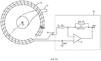
로고스키 코일(Rogowski coil) 센서(12)가 도 1에 도시되어 있다. 가요성 코일(12)은 전류 운반 전도체(10) 주위에서 전도체 회로를 방해하지 않고서 클램핑될 수 있고, 모든 실제 전류 범위들에 걸쳐 선형이고, 이에 따라 AC 전력 산업에서 매력적인 전류 센서 솔루션(solution)을 형성한다. 코일(12) 내에서 중심에 위치된 AC 라인에 의해, 생성된 전압(V)은 하기와 같고:A Rogowski

이때 μ 0는 자유 공간의 투자율이고, n은 코일의 권회수이고, A는 코일 단면적이고, r은 도 1에 도시된 바와 같은 반경이고, I 는 라인 전류이다. 전압(V)은 미분된 라인 전류에 비례하고, 따라서 신호들(V, I)은 90도 위상 차이를 보일 것이다. 전류(I)와 동위상인 신호(V)가 적분을 필요로 할 것이다. 적분은 또한 더 높은 고조파들이 수반되는 경우 정확한 전류 프로파일로 이어질 것이다.Wherein μ 0 is the permeability of free space, n is the turns of the coil, A is the cross-section and the coil, r is the radius as shown in Figure 1, I is the current line. The voltage V is proportional to the differentiated line current, so that the signals V and I will show a 90 degree phase difference. A signal ( V ) that is in phase with the current ( I ) will require integration. The integration will also lead to a correct current profile if higher harmonics are involved.
도 1은 하기의 기본 고조파 전달 함수를 갖는, 단자(16)에서 코일(12)에 결합된 적분기(14)의 일례를 도시한다:1 shows an example of an

도시된 성분 값들을 갖는 적분기(14)는 정확한 위상 정보가 필요할 때 부적절한 솔루션이다. 60 ㎐에서의 RC 곱은 단지 약 1.2이어서, 적분기(14)가 라인 주파수에서 실질적으로 바람직하지 않은 위상 시프트를 갖게 한다. 90도의 원하는 위상 시프트는 R 1을 제거하는 것에 의해 얻어지므로, 전달 함수는 하기의 순수 적분기 형태를 얻는다:The

이러한 전달 함수의 실제 문제는 DC에서의 증폭이 무한대가 된다는 것이다. 그 결과, 출력은 미정의된 DC 레벨을 포함할 수 있는데, 이는 본질적으로 피드백 커패시터(C 1)를 DC 충전된 상태로 남기는 적분 상수를 나타낸다. 스콜라적(Scholastic) 부정 적분법(indefinite integral calculus) 수행들은 적분 상수를 무시하는데, 즉, 그것을 0으로 하는데, 과제는 이제 이러한 편의를 현재의 실제 경우로 확장하는 것이다. 하나의 처리 방안은 피드백 커패시터(C 1)를 가로질러 트랜지스터(MOSFET)를 배치하여 때때로 그것을 방전하여, OPAMP(15) DC 출력이 재정의되도록 하는 것이다. 이러한 접근법은, 드물게 그러나 여전히 규칙적으로 바람직한 순간에 방전하기 위해 타이밍 회로를 필요로 한다. 거의 완벽한 MOSFET들로 잘 구현될 때, 이러한 접근법은 처리 방안을 제공할 수 있다.The real problem with these transfer functions is that the amplification in DC is infinite. As a result, the output may include an undefined DC level, which essentially represents the integral constant that leaves the feedback capacitor C 1 in a DC-charged state. Scholastic indefinite integral calculus runs ignore the integral constant, that is, it is zero, the task is now to extend this convenience to the current real case. One approach is to place a transistor (MOSFET) across the feedback capacitor C 1 to discharge it from time to time, so that the OPAMP 15 DC output is redefined. This approach rarely but still requires a timing circuit to discharge at regularly desired moments. When implemented with nearly perfect MOSFETs, this approach can provide a solution.
따라서, 로고스키 코일들 또는 다른 전류 센서들을 위한 개선된 적분기에 대한 필요성이 존재한다.Thus, there is a need for improved integrators for Rogowski coils or other current sensors.
본 발명에 부합하는, 전류 센서를 위한 적분기 회로는, 전류 센서로부터의 신호를 수신하기 위한 입력을 가지며 전압 신호를 제공하는 출력을 갖는 적분기를 포함한다. 고역 통과 필터는 적분기의 출력에 결합된 입력을 가지며 출력을 갖고, 고역 통과 필터는 전압 신호로부터 DC 콘텐츠를 실질적으로 제거한다. 피드백 루프는 적분기의 출력 및 고역 통과 필터의 출력에 결합된 입력을 가지며, 전압 신호의 DC 콘텐츠를 적분기의 입력에 제공하는 출력을 갖는다.In accordance with the present invention, an integrator circuit for a current sensor includes an integrator having an input for receiving a signal from a current sensor and having an output providing a voltage signal. The high pass filter has an input coupled to the output of the integrator and has an output, and the high pass filter substantially removes the DC content from the voltage signal. The feedback loop has an input coupled to the output of the integrator and an output of the high pass filter and has an output that provides the DC content of the voltage signal to the input of the integrator.
첨부 도면은 본 명세서에 포함되어 그의 일부를 구성하며, 발명의 상세한 설명과 함께 본 발명의 이점 및 원리를 설명한다. 도면에서,
도 1은 로고스키 코일 센서를 위한 종래 기술의 적분 전치증폭기(integrating preamplifier)의 도면이다.
도 2는 로고스키 코일 센서를 위한 적분기 회로의 도면이다.
도 3은 변류기(current transformer) 및 도 2의 적분기 회로에 의해 측정된 라인 전류를 비교하는 그래프이다.
도 4는 도 2의 적분기 회로의 진폭 응답의 그래프이다.
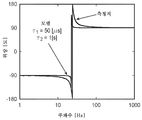
도 5는 도 2의 적분기 회로의 위상 응답의 그래프이다.
도 6은 라인 스텝 전류 및 도 2의 적분기 회로의 임펄스 응답의 그래프이다.BRIEF DESCRIPTION OF THE DRAWINGS The accompanying drawings, which are incorporated in and constitute a part of this specification, illustrate the advantages and principles of the present invention in conjunction with the detailed description of the invention. In the drawings,
Figure 1 is a diagram of a prior art integrating preamplifier for a Rogowski coil sensor.
Figure 2 is a diagram of an integrator circuit for a Rogowski coil sensor.
Figure 3 is a graph comparing the line current measured by the current transformer and the integrator circuit of Figure 2;
Figure 4 is a graph of the amplitude response of the integrator circuit of Figure 2;
Figure 5 is a graph of the phase response of the integrator circuit of Figure 2;
Figure 6 is a graph of the line step current and the impulse response of the integrator circuit of Figure 2;
로고스키 코일 센서 또는 다른 전류 센서들을 위한 개선된 적분기가 개시된다. 로고스키 코일 센서들은 일상적으로 AC 전력 그리드에서 60 ㎐ 라인 전류들을 모니터링 또는 측정하는 데 사용된다. 스마트 그리드 기반시설에서의 발전은 이러한 센서들의 방대한 배치를 필요로 할 것이다. 로고스키 센서들은 구매가능하고, 코일 진폭을 허용가능한 레벨로 끌어올리기 위해 전치증폭기를 필요로 한다. 일반적으로, 로고스키 코일은 대략 라인 전류의 암페어(ampere)당 25 ㎶를 생성하여, 약 1 ㎷/A의 증폭을 선호하는 전자기기를 처리하는 데 직접적으로 사용하기에는 너무 약하다. 상업적인 전치증폭기 또는 트랜스듀서가 이용가능하지만, 이들은 종종 DC 신호를 생성하여, AC 위상 정보의 손실을 초래한다. 라인 전류의 위상 정확한 60 ㎐ 증폭된 복제본을 얻기 위해, 새로운 적분기 설계가 개시된다. 이러한 적분기 설계는 전술된 처리 방안에 대한 개선된 솔루션이고, 피드백 커패시터를 가로질러 어떠한 구성요소의 배치도 필요로 하지 않고, DC 레벨의 연속 모니터링을 이용하지 않고, 안정한 피드백을 통해 그것을 0으로 강제하지 않고서, 순수 적분기 형태에 대한 상기 제2 전달 함수의 고수(adherence)를 수반한다.An improved integrator for a Rogowski coil sensor or other current sensors is disclosed. Rogowski coil sensors are routinely used to monitor or measure 60 Hz line currents in an AC power grid. Evolution in the Smart Grid infrastructure will require extensive deployment of these sensors. Rogowski sensors are available and require a preamplifier to raise the coil amplitude to an acceptable level. In general, Rogowski coils are about too weak to be used directly for processing electronic devices that prefer amplification of about 1 ㎷ / A, producing about 25 당 per ampere of line current. Commercial preamplifiers or transducers are available, but they often generate DC signals, resulting in loss of AC phase information. To obtain a precise 60 Hz amplified replica of the line current, a new integrator design is disclosed. This integrator design is an improved solution to the above-described processing approach, and does not require the placement of any components across the feedback capacitor, without using continuous monitoring of the DC level, , Adherence of the second transfer function to the pure integrator form.
도 2는 3개의 OPAMP들(연산 증폭기들)(21, 22, 23)을 포함하는 적분기 회로(20) 솔루션의 도면이다. 제1 OPAMP(21)는 단자(16)에서 로고스키 코일 센서로부터의 신호를 수신하는 입력을 가지며 신호(V a)를 제공하는 출력(25)을 갖는 순수 적분기이다. OPAMP(21)의 반전 입력은, 예를 들어 1 MΩ의, 접지에 대한 풀다운(pull-down) 저항기를 가질 수 있다. OPAMP(21) 이후에 수동 1차 고역 통과 필터가 뒤따르고, 수동 1차 고역 통과 필터는 커패시터(C 2) 및 저항기(R 2)에 의해 형성되고 신호(V a)를 수신하는 입력을 가지며 적분된 신호의 DC 미포함 버전을 제2 OPAMP(22)의 + 입력으로 전달하는 출력을 갖는데, 제2 OPAMP는 전압 팔로워(voltage follower)로서의 역할을 하고 신호(V b)를 제공하는 출력(26)을 갖는다. 고역 통과 필터는 신호(V a)의 DC 콘텐츠를 제거하거나 또는 회로(20)의 동작을 위해 허용가능한 양만큼 DC 콘텐츠를 실질적으로 제거할 수 있다. 전압 팔로워(OPAMP(22))는 고역 통과 필터 출력에 의해 형성되는 높은 임피던스 지점 상의 부하를 최소화하는 데 사용된다. 제3 OPAMP(23)는 제1 OPAMP(21) 출력의 DC 콘텐츠의 복사본을 생성하는 출력(27)을 갖는 차동 증폭기(이러한 경우에는 증폭하지 않음)이다. 이어서, OPAMP(23)의 출력(V c)으로부터 OPAMP(21)의 + 입력(V +)으로의 DC 피드백 루프를 닫는 것은, 제1 OPAMP(21)의 적분기 출력이 DC 미포함을 유지하는 것을 보장한다.2 is a diagram of an
적분기 회로(20)는 단자(16)에서 로고스키 코일 센서 또는 다른 전류 센서로부터의 신호를 수신하고, 단자(24)에서 출력 신호(V out)를 제공한다. 회로(20)는 단자(24)에서, 전류 센서로부터의 신호에 관련되는 신호, 예를 들어, 전류 센서에 의해 모니터링되는 라인 전도체에서의 큰 전류 스텝에 응답하여 감쇠하는 링잉 신호(ringing signal)를 출력한다. 회로(20)는 출력 단자(24)에서 아날로그-디지털 변환기에 결합되어, 대응하는 디지털 신호를, 예를 들어, 라인 결함 분석과 같은 스마트 그리드 기반시설 모니터링에서 사용하기 위해 프로세서에 제공할 수 있다. 회로(20)는 또한 3상 케이블들에서의 라인 결함을 모니터링 및 검출하는 데 사용될 수 있다.The
회로(20)의 성능은, 변류기(Hammond CT500A)에 의해 그리고 도 2의 적분기 회로(20)에 의해 측정된 라인 전류를 비교하는 도 3에 도시되어 있다. 1 ㎷/A 증폭으로 조정되는 회로(20) 내의 전위차계(R 1)(가변 저항기)에 의해, 도 3에서의 자취들은 극히 작고 일반적으로 허용가능한 위상 차이를 갖는 거의 완벽한 대응을 보여준다.The performance of the
하기는 회로(20)의 동작의 고조파 분석을 제공한다. 비반전 입력 전압(V+)이 접지 전위에 있는 경우, 제1 OPAMP(21) 적분기의 전달 함수는 하기와 같다:The following provides a harmonic analysis of the operation of the
![]()
![]()
수학식 1에서의 함수는 극도로 높은 증폭을 갖는 DC 또는 더 현실적으로는 매우 낮은 주파수에서 소정의 폴(pole)을 갖는 이상적인 적분기의 함수이다. 이러한 예시적인 경우에서와 같이, 주요 응용이 60 ㎐ 신호에 대한 적분기를 형성하는 경우, 저주파수 잡음의 적분은 큰 진폭을 갖는 느리게 변하는 드리프트(drift)를 초래하는데, 이는 성가신 존재(nuisance)가 된다. 이러한 성가신 존재는 적분기 DC 상태를 때때로 재설정함으로써 또는 관심 대상이 아닌 저주파수들에서의 증폭을 제한함으로써 회피될 수 있다.The function in Equation (1) is a function of an ideal integrator having a pole at a very high amplification DC or, more practically, at a very low frequency. If, as in this exemplary case, the main application forms an integrator for a 60 Hz signal, the integration of the low frequency noise results in a slowly varying drift with a large amplitude, which becomes a nuisance. This annoying presence can be avoided by resetting the integrator DC state from time to time or by restricting amplification at low frequencies not of interest.
따라서, 하나의 처리 방안은, 효과적이긴 하지만 가장 명쾌한 솔루션은 아닌, MOSFET를 통해 커패시터(C 1)를 단락시킴으로써 그것을 때때로 방전시키는 것을 수반한다. 저주파수들에서의 증폭을 제한하기 위한 다른 통상의 처리 방안은, 커패시터(C 1)를 가로질러 큰 피드백 저항기(R f)를 배치하여, DC에서의 증폭이 저항기들(R f, R 1)의 비(R f/R 1)와 최대한 동일하게 하는 것이다. 실제로, 이러한 비는 1보다 여전히 훨씬 더 커서, 느린 드리프트의 성가신 존재는 감소되지만 제거되지는 않게 된다. 증폭이 DC에서 0에 근접하는 경향이 있는 경우에 추가의 개선이 얻어질 수 있다. 그러한 것은 하기의 고조파 분석이 증명하는 바와 같이 도 2의 회로(20)를 갖는 경우이다.Thus, one approach involves discharging it occasionally by shorting the capacitor C 1 through the MOSFET, but not the most clever solution. The other conventional treatment methods for limiting the amplification in the low frequency, the capacitor by placing a large feedback resistor (R f) across a (C 1), the amplification of the DC resistor (R f, R 1) Ratio ( R f / R 1 ). In practice, this ratio is still much larger than 1, so that the annoying presence of slow drift is reduced, but not eliminated. A further improvement can be obtained if the amplification tends to approach zero at DC. This is the case with the
도 2에 나타낸 전압들은 모두 접지를 기준으로 한다. 각주파수(ω)에 의해, 2개의 기본 전달 함수들이 하기에 의해 제공되고:The voltages shown in Fig. 2 are all based on the ground. By the angular frequency [omega], two basic transfer functions are provided by:

이때 모든 저항기들(R들)은 동일한 값을 갖는다:Where all resistors ( R ) have the same value:
![]()
![]()
임의의 V + 입력 전압을 고려하면, 제1 OPAMP(21) 적분기 전달 함수의 유도는 하기의 2개의 수학식들을 필요로 한다:Taking into account any V + input voltage, the derivation of the first OPAMP (21) integrator transfer function requires the following two equations:

수학식 4 및 수학식 5로부터 전류(i)를 제거하면 하기와 같다:The current ( i ) is removed from Equations (4) and (5) as follows:

회로(20)에 도시된 바와 같이, 직접 피드백을 통해 전압(V +)을 전압(V c)과 같게 하고, 수학식 2, 수학식 3 및 수학식 6을 조합하면 하기와 같다:As shown in the

명백하게, 수학식 7은 τ 2 >> τ 1인 경우 이상적인 적분기에 근접하고, 결과 자체는 전체 적분기 전달 함수가 하기와 같이 유도되는 경우 나타난다:Obviously, equation (7) approximates an ideal integrator in the case of τ 2 >> τ 1 , and the result itself appears when the overall integrator transfer function is derived as:

수학식 8에서의 전체 전달 함수는 하기 2개의 조건들이 둘 모두 충족될 때 우수한 적분기가 된다:The overall transfer function in equation (8) becomes an excellent integrator when both of the following two conditions are met:

바람직한 이점은 ω가 DC에 근접할 때 명백해지는데, 이는 그때 출력이 ωτ 2 항에 관련되는 미분의 결과로서 제거되기 때문이다. 이것은 DC에서의 증폭이 무한대인 경향이 있는 수학식 1에서의 순수 적분기와는 다르다.A preferred advantage is apparent when ? Is close to DC because the output is then removed as a result of the derivative associated with ? 2 . This is different from the pure integrator in equation (1) where the amplification at DC tends to be infinite.
특성들은, 도 4 및 도 5에 예시된 바와 같이, 수학식 8에서의 전달 함수의 진폭 응답 및 위상 응답을 플로팅함으로써 추가로 증명된다. 도 4에서의 회로(20)의 진폭 응답은 적분 목적을 위한 사용가능한 주파수 범위의 절대 하한을 표시하는 공진 피크를 명백하게 보여준다. 진폭이 최대치 τ 2/(2τ 1)인 상태에서 수학식 8의 위상을 0으로 설정함으로써 공진 주파수(f res)가 하기와 같이 얻어진다:The properties are further verified by plotting the amplitude response and the phase response of the transfer function in equation (8), as illustrated in Figures 4 and 5. The amplitude response of the

60 ㎐ AC 라인 전류 적분기의 경우, 설계 고려사항은 f res가 약 10 ㎐를 초과하지 않게 하는 것일 수 있다. 회로(20)는 저잡음 환경, 특히 f res 근처를 필요로 하는데, 이는 단색성 60 ㎐ 라인 신호의 경우 편안하게 가정될 수 있다.For 60 ㎐ AC line current integrator, design considerations may be to the f res does not exceed about 10
추가 예시 목적을 위해, 회로(20)의 동작은 커패시터(C 1)를 가로질러 저항기(R f)를 배치함으로써 형성된 1차 필터 회로와 비교될 수 있다. 그러한 비교는 단지 수 헤르츠(hertz) 대역폭에만 걸쳐 연장되는 미분으로부터 적분으로의 극도로 예리한 전이로 회로(20)의 이점들을 증명할 것이다.For further illustrative purposes, the operation of
하기는 회로(20)의 임펄스 응답의 과도상태 분석을 제공한다. 회로(20)의 라플라스(Laplace) 변환된 전달 함수는 하기와 같이 유도되고:The following provides an analysis of the transient state of the impulse response of the

수학식 10에 또한 나타난 바와 같이, 루트(r)를 정의하면 하기와 같다:As also shown in equation (10), root ( r ) is defined as follows:

주파수들(ω 1, ω 2)은 복소 공액들로서 하기와 같이 평가된다:The frequencies ω 1 , ω 2 are evaluated as complex conjugates as follows:

맥스웰 방정식(Maxwell's equation)들에 기초하여, 저항으로 종단되는 로고스키 코일 인덕턴스가 1차 미분 방정식에 의해 적절히 설명된다. 그때 임펄스 응답들은 시간의 지수 표현 형태를 갖는다. 유사하게, 10 nF 커패시터 및 50 Ω 저항 분배기에 걸쳐 광대역 함수 발생기로부터의 느린 100 m㎐ 구형파를 미분함으로써 지수 형태의 임펄스 응답이 얻어질 수 있다. 그러한 임펄스는 하기에 의해 설명된다:Based on Maxwell's equations, the Rogowski coil inductance terminated by a resistor is suitably described by a first-order differential equation. The impulse responses then have the exponential representation of time. Similarly, an impulse response in exponential form can be obtained by differentiating a slow 100 mHz square wave from a broadband function generator over a 10 nF capacitor and a 50 Ω resistor divider. Such an impulse is described by:

이때 ω 0는 실수이며 양의 값이고, 라플라스 변환하면 하기와 같다:Where ω 0 is a real number and a positive value, and the Laplace transform is:

수학식 10에 수학식 15를 대입하면, 임펄스 응답 스펙트럼은 하기와 같이 된다:Substituting Equation (15) into Equation (10), the impulse response spectrum is:

회로(20)의 역라플라스 변환된 임펄스 응답은 V 0 τ 0 = M I ac의 입력 임펄스 콘텐츠를 이용하여 하기의 수학식 17에서 제공되는데, 이때 M은 상호 인덕턴스의 로고스키 코일 계수이고 I ac는 도 6에 도시된 전류 스텝 진폭이다.The inverse Laplace transformed impulse response of

수학식 17은 |ω 0| >> |ω 1|, |ω 2|일 때 매우 양호한 근사치이고, 항상 감쇠하는 임펄스 응답 솔루션들로 적분기 회로 안정성을 증명한다. 수학식 17에 의해, 적분기를 60 ㎐ 라인 주파수 훨씬 미만의 공진 주파수를 갖는 전자 소리굽쇠(tuning fork)로서 생각할 수 있다.Equation (17) ω 0 | >> | ω 1 |, | It is a very good approximation when ω 2 │ and demonstrates the integrator circuit stability with constantly attenuating impulse response solutions. By means of Equation (17), the integrator can be thought of as an electronic tuning fork with a resonance frequency well below the 60 Hz line frequency.
도 6은 250 A의 실제 라인 전류 스텝 및 결과적인 적분기 회로(20) 링잉 응답을 도시하는, 회로(20)의 라인 전류 스텝 응답의 그래프이다.6 is a graph of the line current step response of the
회로(20) 내의 저항기들 및 커패시터들에 대해 제공된 예시적인 구성요소 값들은 옴(ohm) 및 패럿(farad) 단위이다. 예를 들어, 회로(20)의 특정 응용에 따라 다른 구성요소 값들이 사용될 수 있다. 구성요소가 다른 구성요소에 결합된 것으로 기술될 때, 구성요소들은 직접 결합되거나 또는 그들 사이의 전기 통신을 위한 다른 구성요소들을 통해 결합될 수 있다. 구성요소에 대한 입력이라는 용어는 단일 입력 또는 다수의 입력들을 포함할 수 있다. 구성요소로부터의 출력이라는 용어는 단일 출력 또는 다수의 출력들을 포함할 수 있다.Exemplary component values provided for the resistors and capacitors in
Claims (19)
전류 센서로부터의 신호를 수신하기 위한 입력을 가지며 전압 신호를 제공하는 출력을 갖는 적분기;
적분기의 출력에 결합된 입력을 가지며 출력을 갖고, 전압 신호로부터 DC 콘텐츠를 실질적으로 제거하는 고역 통과 필터; 및
적분기의 출력 및 고역 통과 필터의 출력에 결합된 입력을 가지며 전압 신호의 DC 콘텐츠를 적분기의 입력에 제공하는 출력을 갖는 피드백 루프를 포함하는 적분기 회로.An integrator circuit for a current sensor,
An integrator having an input for receiving a signal from the current sensor and having an output providing a voltage signal;
A high pass filter having an input coupled to the output of the integrator and having an output, the filter substantially removing DC content from the voltage signal; And
A feedback loop having an output coupled to the output of the integrator and an output coupled to the output of the high pass filter and having an output providing the DC content of the voltage signal to the input of the integrator.
전류 센서로부터의 신호를 수신하기 위한 입력을 가지며 전압 신호를 제공하는 출력을 갖는 적분기;
적분기의 출력에 결합된 입력을 가지며 출력을 갖고, 전압 신호로부터 DC 콘텐츠를 실질적으로 제거하는 고역 통과 필터;
고역 통과 필터의 출력에 결합된 입력을 가지며 출력을 갖는 전압 팔로워; 및
적분기의 출력에 결합된 제1 입력, 전압 팔로워의 출력에 결합된 제2 입력, 및 전압 신호의 DC 콘텐츠를 적분기의 입력에 제공하는 출력을 갖는 차동 증폭기를 포함하고,
전압 팔로워의 출력은 전류 센서로부터의 신호에 관련되는 신호를 제공하는 적분기 회로.An integrator circuit for a current sensor,
An integrator having an input for receiving a signal from the current sensor and having an output providing a voltage signal;
A high pass filter having an input coupled to the output of the integrator and having an output, the filter substantially removing DC content from the voltage signal;
A voltage follower having an input coupled to an output of the high pass filter and having an output; And
A differential amplifier having a first input coupled to the output of the integrator, a second input coupled to the output of the voltage follower, and an output providing the DC content of the voltage signal to the input of the integrator,
The output of the voltage follower provides a signal related to the signal from the current sensor.
전류 전도체에 근접하게 위치되어 전도체에서의 전류를 검출하기 위한 전류 센서; 및
전류 센서에 결합된 적분기 회로를 포함하고, 적분기 회로는,
전류 센서로부터의 신호를 수신하기 위한 입력을 가지며 전압 신호를 제공하는 출력을 갖는 적분기;
적분기의 출력에 결합된 입력을 가지며 출력을 갖고, 전압 신호로부터 DC 콘텐츠를 실질적으로 제거하는 고역 통과 필터; 및
적분기의 출력 및 고역 통과 필터의 출력에 결합된 입력을 가지며 전압 신호의 DC 콘텐츠를 적분기의 입력에 제공하는 출력을 갖는 피드백 루프를 포함하는 시스템.A system for monitoring current, comprising:
A current sensor positioned proximate to the current conductor to detect current in the conductor; And
And an integrator circuit coupled to the current sensor,
An integrator having an input for receiving a signal from the current sensor and having an output providing a voltage signal;
A high pass filter having an input coupled to the output of the integrator and having an output, the filter substantially removing DC content from the voltage signal; And
A feedback loop having an output coupled to the output of the integrator and an output of the high pass filter and having an output providing the DC content of the voltage signal to an input of an integrator.
Applications Claiming Priority (3)
| Application Number | Priority Date | Filing Date | Title |
|---|---|---|---|
| US14/613,589 | 2015-02-04 | ||
| US14/613,589 US9588147B2 (en) | 2015-02-04 | 2015-02-04 | Electronic integrator for Rogowski coil sensors |
| PCT/US2016/013783 WO2016126406A1 (en) | 2015-02-04 | 2016-01-18 | Electronic integrator for rogowski coil sensors |
Publications (1)
| Publication Number | Publication Date |
|---|---|
| KR20170110103A true KR20170110103A (en) | 2017-10-10 |
Family
ID=56554090
Family Applications (1)
| Application Number | Title | Priority Date | Filing Date |
|---|---|---|---|
| KR1020177023853A KR20170110103A (en) | 2015-02-04 | 2016-01-18 | Electronic integrator for Rogowski coil sensor |
Country Status (7)
| Country | Link |
|---|---|
| US (1) | US9588147B2 (en) |
| EP (1) | EP3254123A4 (en) |
| JP (1) | JP2018504605A (en) |
| KR (1) | KR20170110103A (en) |
| CN (1) | CN107209211B (en) |
| CA (1) | CA2975688A1 (en) |
| WO (1) | WO2016126406A1 (en) |
Cited By (1)
| Publication number | Priority date | Publication date | Assignee | Title |
|---|---|---|---|---|
| KR101984073B1 (en) * | 2018-06-15 | 2019-05-31 | 주식회사 엘피에스코리아 | Impulse current measurement device using rogowski coil |
Families Citing this family (10)
| Publication number | Priority date | Publication date | Assignee | Title |
|---|---|---|---|---|
| US10690699B2 (en) | 2016-06-21 | 2020-06-23 | 3M Innovative Properties Company | Holder with self-aligning feature for holding current sensor around line conductor |
| TWI629486B (en) * | 2016-09-14 | 2018-07-11 | 台達電子工業股份有限公司 | Current sensing apparatus and method of operating the same |
| EP3296752B1 (en) * | 2016-09-15 | 2024-01-10 | General Electric Technology GmbH | Improvements in or relating to the measurement of current within a conductor |
| US11026068B2 (en) | 2017-01-05 | 2021-06-01 | 3M Innovative Properties Company | Wireless sensor communication system for enclosures |
| CN110619175B (en) * | 2019-09-17 | 2020-12-01 | 贵州电网有限责任公司 | Dynamic attenuation integral reduction method for acquisition unit of electronic transformer |
| CN110798157A (en) * | 2019-11-15 | 2020-02-14 | 广州供电局有限公司 | Rogowski coil integrator |
| IT202000019285A1 (en) * | 2020-08-05 | 2022-02-05 | Areti S P A | CONDITIONER CIRCUIT, GROUP AND SYSTEM FOR THE MEASUREMENT OF AN ELECTRIC SIGNAL |
| US11740265B1 (en) * | 2022-06-09 | 2023-08-29 | Accuenergy (Canada) Inc. | Signal conditioning circuit |
| US20230402832A1 (en) * | 2022-06-09 | 2023-12-14 | Accuenergy (Canada) Inc. | Integrator for protective relay |
| DE102022117871B4 (en) | 2022-07-18 | 2024-03-14 | Infineon Technologies Ag | CURRENT SENSOR, SYSTEM WITH A CURRENT SENSOR AND METHOD FOR MEASURING A CURRENT TO BE MEASURED |
Family Cites Families (25)
| Publication number | Priority date | Publication date | Assignee | Title |
|---|---|---|---|---|
| US2969183A (en) | 1958-05-06 | 1961-01-24 | Jr Herbert B Voelcker | Positive feedback electronic integrator and differentiator circuits |
| US3610908A (en) | 1970-02-09 | 1971-10-05 | Cutler Hammer Inc | Electronic integrator system |
| US4035809A (en) | 1975-12-29 | 1977-07-12 | John Kenneth Jacobsen | Electronic integrator for chart recorder |
| DD126867A1 (en) | 1976-08-13 | 1977-08-17 | ||
| JPS5547729A (en) * | 1978-10-02 | 1980-04-04 | Tamagawa Seiki Kk | Variable time constant unit |
| US5539354A (en) * | 1993-08-18 | 1996-07-23 | Carsten; Bruce W. | Integrator for inductive current sensor |
| JP2001521629A (en) * | 1997-04-21 | 2001-11-06 | リエゾン,エレクトロニク−メカニク,エルウエム,ソシエテ,アノニム | Apparatus for measuring conductor current intensity with wide passband |
| JPH1133744A (en) | 1997-07-17 | 1999-02-09 | Dengensha Mfg Co Ltd | Method and device to control current for resistance welding |
| JPH11281678A (en) | 1998-03-30 | 1999-10-15 | Shimadzu Corp | Current sensor |
| ATE262682T1 (en) | 1998-04-22 | 2004-04-15 | Power Electronic Measurements | CURRENT MEASUREMENT DEVICE |
| US6919835B2 (en) | 2002-12-16 | 2005-07-19 | General Electric Company | Infinite electronic integrator |
| JP4156412B2 (en) * | 2003-03-13 | 2008-09-24 | 三菱電機株式会社 | Current sensor |
| CN100394199C (en) * | 2004-05-18 | 2008-06-11 | 华中科技大学 | Direct current sensor |
| JP2007044813A (en) | 2005-08-10 | 2007-02-22 | Fanuc Ltd | Electric discharge machining device |
| JP2007081845A (en) * | 2005-09-14 | 2007-03-29 | Fujitsu Ten Ltd | Sinusoidal signal generator |
| US7679162B2 (en) * | 2005-12-19 | 2010-03-16 | Silicon Laboratories Inc. | Integrated current sensor package |
| CN100439926C (en) * | 2006-03-31 | 2008-12-03 | 北京万工科技有限公司 | Integrator for Rogowski coil and its realizing method |
| US7532000B2 (en) * | 2006-08-03 | 2009-05-12 | The Boeing Company | Method and system for measurement of current flows in fastener arrays |
| BRPI0910971A2 (en) | 2008-04-04 | 2015-10-06 | Schweitzer Engineering Lab Inc | Failed Circuit Indicator, Method for Installing a Failed Three-Phase Circuit Indicator on a Three-Phase Power Cable, and System for Detecting a Failed Current on a Multi-Conductor Power Cable |
| JP5423413B2 (en) * | 2009-05-29 | 2014-02-19 | ソニー株式会社 | Angular velocity sensor, angular velocity signal amplification circuit, electronic device, camera shake correction device, angular velocity signal amplification method, and camera shake correction method |
| CN102128966B (en) * | 2011-01-11 | 2012-07-11 | 沈阳互感器有限责任公司 | Rogowski coil-based integrator circuit for electronic current transformer |
| US8761853B2 (en) * | 2011-01-20 | 2014-06-24 | Nitto Denko Corporation | Devices and methods for non-invasive optical physiological measurements |
| EP2672282A1 (en) * | 2012-06-07 | 2013-12-11 | ABB Oy | Earth fault detection in frequency converter |
| US9921243B2 (en) | 2012-12-17 | 2018-03-20 | Covidien Lp | System and method for voltage and current sensing |
| CN203231777U (en) * | 2013-04-01 | 2013-10-09 | 燕山大学 | Drive circuit of electromagnetic flowmeter |
-
2015
- 2015-02-04 US US14/613,589 patent/US9588147B2/en active Active
-
2016
- 2016-01-18 CN CN201680008654.6A patent/CN107209211B/en not_active Expired - Fee Related
- 2016-01-18 CA CA2975688A patent/CA2975688A1/en not_active Abandoned
- 2016-01-18 EP EP16746949.3A patent/EP3254123A4/en not_active Withdrawn
- 2016-01-18 JP JP2017541065A patent/JP2018504605A/en not_active Ceased
- 2016-01-18 WO PCT/US2016/013783 patent/WO2016126406A1/en active Application Filing
- 2016-01-18 KR KR1020177023853A patent/KR20170110103A/en unknown
Cited By (1)
| Publication number | Priority date | Publication date | Assignee | Title |
|---|---|---|---|---|
| KR101984073B1 (en) * | 2018-06-15 | 2019-05-31 | 주식회사 엘피에스코리아 | Impulse current measurement device using rogowski coil |
Also Published As
| Publication number | Publication date |
|---|---|
| JP2018504605A (en) | 2018-02-15 |
| WO2016126406A1 (en) | 2016-08-11 |
| CN107209211B (en) | 2019-12-06 |
| CA2975688A1 (en) | 2016-08-11 |
| CN107209211A (en) | 2017-09-26 |
| EP3254123A4 (en) | 2018-11-21 |
| US20160223592A1 (en) | 2016-08-04 |
| EP3254123A1 (en) | 2017-12-13 |
| US9588147B2 (en) | 2017-03-07 |
Similar Documents
| Publication | Publication Date | Title |
|---|---|---|
| KR20170110103A (en) | Electronic integrator for Rogowski coil sensor | |
| US9459291B2 (en) | Voltage detection device | |
| CN107003340B (en) | Current sensor and measuring device | |
| KR101735776B1 (en) | Power line monitoring methodology and its device for detection of certain harmonic frequency based on contactless pick-up coil including signal mixing and resonance circuit | |
| US20180164347A1 (en) | Apparatus and method for measuring an electric current in an electrical conductor | |
| US9645193B2 (en) | Impedance source ranging apparatus and method | |
| CN104515931B (en) | A kind of DC leakage flow sensor based on magnetic modulation | |
| Bak-Jenson et al. | Parametric identification in potential transformer modelling | |
| CN106685376B (en) | Fractional order inductance circuit | |
| AU2020319634A1 (en) | Current sensors employing Rogowski coils and methods of using same | |
| US9264028B2 (en) | Zero crossing detector using current mode approach | |
| JP2017083379A (en) | Impedance measuring device and impedance measuring method | |
| CN110261668A (en) | Current detection circuit and detection method | |
| WO2018050741A1 (en) | Improvements in or relating to the measurement of current within a conductor | |
| JP2013029349A (en) | Impulse current detection device | |
| US6777959B2 (en) | Method of determining a resistive current | |
| US10782324B2 (en) | Device and method for measuring electrical current in an electrical conductor | |
| JP5312905B2 (en) | Resistance measuring device | |
| JP5758229B2 (en) | Magnetic field detector | |
| JP3034651B2 (en) | Diagnosis method for insulation of CV cable | |
| JP5274920B2 (en) | Resistance measuring device | |
| JPS596137Y2 (en) | Insulation monitoring device for rotating machine windings | |
| JPH10246740A (en) | Method and device for measuring harmonic by capacitor type potential transformer | |
| RU2388000C2 (en) | Method for measuring bridge signal processing and device for its implementation | |
| CN116436283A (en) | Active common mode electromagnetic interference filter |