KR20170093949A - Detection of lost wafer from spinning chuck - Google Patents
Detection of lost wafer from spinning chuck Download PDFInfo
- Publication number
- KR20170093949A KR20170093949A KR1020177019065A KR20177019065A KR20170093949A KR 20170093949 A KR20170093949 A KR 20170093949A KR 1020177019065 A KR1020177019065 A KR 1020177019065A KR 20177019065 A KR20177019065 A KR 20177019065A KR 20170093949 A KR20170093949 A KR 20170093949A
- Authority
- KR
- South Korea
- Prior art keywords
- detection
- microelectronic substrate
- component
- position indicator
- rotating chuck
- Prior art date
Links
Images


Classifications
-
- H—ELECTRICITY
- H01—ELECTRIC ELEMENTS
- H01L—SEMICONDUCTOR DEVICES NOT COVERED BY CLASS H10
- H01L21/00—Processes or apparatus adapted for the manufacture or treatment of semiconductor or solid state devices or of parts thereof
- H01L21/67—Apparatus specially adapted for handling semiconductor or electric solid state devices during manufacture or treatment thereof; Apparatus specially adapted for handling wafers during manufacture or treatment of semiconductor or electric solid state devices or components ; Apparatus not specifically provided for elsewhere
- H01L21/67005—Apparatus not specifically provided for elsewhere
- H01L21/67242—Apparatus for monitoring, sorting or marking
- H01L21/67288—Monitoring of warpage, curvature, damage, defects or the like
-
- H—ELECTRICITY
- H01—ELECTRIC ELEMENTS
- H01L—SEMICONDUCTOR DEVICES NOT COVERED BY CLASS H10
- H01L21/00—Processes or apparatus adapted for the manufacture or treatment of semiconductor or solid state devices or of parts thereof
- H01L21/67—Apparatus specially adapted for handling semiconductor or electric solid state devices during manufacture or treatment thereof; Apparatus specially adapted for handling wafers during manufacture or treatment of semiconductor or electric solid state devices or components ; Apparatus not specifically provided for elsewhere
- H01L21/683—Apparatus specially adapted for handling semiconductor or electric solid state devices during manufacture or treatment thereof; Apparatus specially adapted for handling wafers during manufacture or treatment of semiconductor or electric solid state devices or components ; Apparatus not specifically provided for elsewhere for supporting or gripping
- H01L21/687—Apparatus specially adapted for handling semiconductor or electric solid state devices during manufacture or treatment thereof; Apparatus specially adapted for handling wafers during manufacture or treatment of semiconductor or electric solid state devices or components ; Apparatus not specifically provided for elsewhere for supporting or gripping using mechanical means, e.g. chucks, clamps or pinches
- H01L21/68714—Apparatus specially adapted for handling semiconductor or electric solid state devices during manufacture or treatment thereof; Apparatus specially adapted for handling wafers during manufacture or treatment of semiconductor or electric solid state devices or components ; Apparatus not specifically provided for elsewhere for supporting or gripping using mechanical means, e.g. chucks, clamps or pinches the wafers being placed on a susceptor, stage or support
- H01L21/68728—Apparatus specially adapted for handling semiconductor or electric solid state devices during manufacture or treatment thereof; Apparatus specially adapted for handling wafers during manufacture or treatment of semiconductor or electric solid state devices or components ; Apparatus not specifically provided for elsewhere for supporting or gripping using mechanical means, e.g. chucks, clamps or pinches the wafers being placed on a susceptor, stage or support characterised by a plurality of separate clamping members, e.g. clamping fingers
-
- H—ELECTRICITY
- H01—ELECTRIC ELEMENTS
- H01L—SEMICONDUCTOR DEVICES NOT COVERED BY CLASS H10
- H01L21/00—Processes or apparatus adapted for the manufacture or treatment of semiconductor or solid state devices or of parts thereof
- H01L21/67—Apparatus specially adapted for handling semiconductor or electric solid state devices during manufacture or treatment thereof; Apparatus specially adapted for handling wafers during manufacture or treatment of semiconductor or electric solid state devices or components ; Apparatus not specifically provided for elsewhere
- H01L21/683—Apparatus specially adapted for handling semiconductor or electric solid state devices during manufacture or treatment thereof; Apparatus specially adapted for handling wafers during manufacture or treatment of semiconductor or electric solid state devices or components ; Apparatus not specifically provided for elsewhere for supporting or gripping
- H01L21/687—Apparatus specially adapted for handling semiconductor or electric solid state devices during manufacture or treatment thereof; Apparatus specially adapted for handling wafers during manufacture or treatment of semiconductor or electric solid state devices or components ; Apparatus not specifically provided for elsewhere for supporting or gripping using mechanical means, e.g. chucks, clamps or pinches
- H01L21/68714—Apparatus specially adapted for handling semiconductor or electric solid state devices during manufacture or treatment thereof; Apparatus specially adapted for handling wafers during manufacture or treatment of semiconductor or electric solid state devices or components ; Apparatus not specifically provided for elsewhere for supporting or gripping using mechanical means, e.g. chucks, clamps or pinches the wafers being placed on a susceptor, stage or support
- H01L21/68764—Apparatus specially adapted for handling semiconductor or electric solid state devices during manufacture or treatment thereof; Apparatus specially adapted for handling wafers during manufacture or treatment of semiconductor or electric solid state devices or components ; Apparatus not specifically provided for elsewhere for supporting or gripping using mechanical means, e.g. chucks, clamps or pinches the wafers being placed on a susceptor, stage or support characterised by a movable susceptor, stage or support, others than those only rotating on their own vertical axis, e.g. susceptors on a rotating caroussel
Abstract
본 개시는 마이크로 전자 기판이 회전 척으로부터 더 이상 제대로 고정되지 않거나 손실되었을 때를 검출하기 위한 시스템 및 방법에 관한 것이다. 마이크로 전자 기판은 프로세스 챔버에서의 처리 동안 기판을 화학 물질에 노출시킬 때 기판을 회전시킬 수 있는 회전 척에 고정될 수 있다. 회전 척은 마이크로 전자 기판을 고정하는 그립핑 메커니즘의 위치를 검출하기 위해 하나 이상의 검출기들을 포함할 수 있다. 검출기들은 마이크로 전자 기판의 위치와 관련되는 전기 신호를 생성할 수 있다. 전기 신호(들)이 문턱값을 초과하면, 시스템이 척의 회전을 정지시켜 프로세스 챔버에 대한 추가 손상을 방지할 수 있다.The present disclosure relates to a system and method for detecting when a microelectronic substrate is no longer properly secured or lost from a rotating chuck. The microelectronic substrate may be secured to a rotating chuck capable of rotating the substrate when exposing the substrate to chemicals during processing in the process chamber. The rotating chuck may include one or more detectors to detect the position of the gripping mechanism that holds the microelectronic substrate. The detectors may generate an electrical signal associated with the position of the microelectronic substrate. If the electrical signal (s) exceeds the threshold, the system can stop the rotation of the chuck to prevent further damage to the process chamber.
Description
본 발명은 마이크로 전자 기판의 표면을 처리하기 위한 장치 및 방법에 관한 것으로, 특히, 마이크로 전자 기판이 처리 중에 제 위치에 고정되었는지 여부를 결정하기 위한 장치 및 방법에 관한 것이다.The present invention relates to an apparatus and method for treating a surface of a microelectronic substrate, and more particularly, to an apparatus and method for determining whether a microelectronic substrate is held in place during processing.
계속 증가하는 능동 컴포넌트의 밀도를 갖는 집적 회로(IC)가 반도체 기판과 같은 마이크로 전자 기판 상에 형성될 수 있다. IC는 필요에 따라 전기적 기능을 수행하는 구조물을 형성하는 연속적인 프로세스 처리를 통해 형성될 수 있다. 마이크로 전자 기판의 프로세싱은, 마이크로 전자 기판을 제어된 방식으로 고정 및 처리하기 위해 자동화될 수 있다. 일 양태는 처리 또는 프로세싱 중에 마이크로 전자 기판을 회전시키는 것을 포함할 수 있다. 회전은 마이크로 전자 기판에 걸쳐 보다 균일한 프로세싱을 가능하게 할 수 있다. 그러나, 회전 속도가 비교적 높을 수 있어, 마이크로 전자 기판이 고정되지 않게 되는 경우, 기판은 파손될 수 있고 프로세싱 장비는 손상될 수 있다. 따라서, 마이크로 전자 기판이 고정되지 않게 되는 때를 결정하고, 회전 메커니즘을 디스에이블시켜 기판 파손의 가능성을 줄이고, 느슨한 마이크로 전자 기판에 의해 야기되는 장비의 손상을 방지하거나 최소화하는 것이 바람직할 수 있다.An integrated circuit (IC) having an ever increasing density of active components can be formed on a microelectronic substrate such as a semiconductor substrate. The IC may be formed through a continuous process process that forms a structure that performs an electrical function as needed. The processing of the microelectronic substrate can be automated to fix and process the microelectronic substrate in a controlled manner. One aspect may include rotating the microelectronic substrate during processing or processing. The rotation can enable more uniform processing across the microelectronic substrate. However, the rotational speed can be relatively high, and if the microelectronic substrate is not fixed, the substrate can be broken and the processing equipment can be damaged. Thus, it may be desirable to determine when the microelectronic substrate becomes unstable, to disable the rotation mechanism to reduce the possibility of substrate breakage, and to prevent or minimize damage to equipment caused by loose microelectronic substrates.
마이크로 전자 디바이스 제조 산업에서, 디바이스들이 반도체 프로세싱 장비에 의해 전달되고, 취급되며, 처리되는 마이크로 전자 기판(예를 들어, 반도체 웨이퍼) 상에 제조된다. 마이크로 전자 기판의 직경은 150mm보다 클 수 있으며, 프로세스 장비에 의한 여러 타입의 기계적 핸들링의 대상이 될 수 있다. 기계적 핸들링의 일 양태는, 처리 동안 마이크로 전자 기판을 회전시키는 것을 포함할 수 있지만, 이에 제한되는 것은 아니다. 기계적 핸들링은 적어도 50rpm의 속도로 회전시킬 수 있는 회전 메커니즘에 마이크로 전자 디바이스를 고정하는 것을 포함할 수 있다. 대부분의 경우, 고정된 마이크로 전자 디바이스는 성공적으로 처리되고 사고 없이 프로세스 장비로부터 제거된다. 그러나, 어떤 경우에는, 마이크로 전자 기판이 회전 메커니즘으로부터 고정되지 않게 될 수 있다. 이것은 기판의 파손 및 프로세스 챔버의 손상을 야기할 수 있으며, 이는 회전 메커니즘이 계속 회전하고 챔버 전체에 걸쳐 파손된 마이크로 전자 기판의 부분이 돌출되는 경우, 증가될 수 있다.In the microelectronic device manufacturing industry, devices are fabricated on microelectronic substrates (e.g., semiconductor wafers) that are delivered, handled, and processed by semiconductor processing equipment. The diameter of the microelectronic substrate can be greater than 150 mm and can be subject to several types of mechanical handling by process equipment. One aspect of mechanical handling can include, but is not limited to, rotating the microelectronic substrate during processing. The mechanical handling may include securing the microelectronic device to a rotating mechanism capable of rotating at a speed of at least 50 rpm. In most cases, fixed microelectronic devices are successfully processed and removed from process equipment without incident. However, in some cases, the microelectronic substrate may become unfixed from the rotation mechanism. This can cause breakage of the substrate and damage to the process chamber, which can be increased if the rotating mechanism continues to rotate and a portion of the broken microelectronic substrate over the entire chamber is projected.
프로세스 장비의 손상을 방지하거나 최소화하기 위한 하나의 방식은, 마이크로 전자 기판이 마이크로 전자 기판의 회전 이전에 그리고 회전 동안에 고정되었는지 여부를 결정하는 마이크로 전자 기판 검출 시스템을 포함할 수 있다. 일 실시예에서, 마이크로 전자 기판을 회전시키는 것을 포함할 수 있는 후속 처리를 위해 원하는 위치에 마이크로 전자 기판을 고정시키는 임의의 기계적 수단(예를 들어, 클램프)을 사용하여, 마이크로 전자 기판은 그립핑(gripping)될 수 있다. 그립핑 메커니즘의 위치 결정(positioning)은, 검출 시스템에 의해 모니터링될 수 있어, 메커니즘이 바람직하지 않은 방식으로 위치를 변경하면, 검출 시스템은 프로세스 챔버 손상을 최소화하기 위해 회전을 셧 다운(shut down)시킬 수 있다.One way to prevent or minimize damage to the process equipment may include a microelectronic substrate detection system that determines whether the microelectronic substrate is fixed before and during rotation of the microelectronic substrate. In one embodiment, using any mechanical means (e.g., a clamp) to secure the microelectronic substrate to a desired location for subsequent processing, which may involve rotating the microelectronic substrate, the microelectronic substrate may be gripped and can be gripped. The positioning of the gripping mechanism can be monitored by the detection system so that when the mechanism changes position in an undesirable manner the detection system will shut down the rotation to minimize process chamber damage, .
일 실시예에서, 회전 메커니즘은 마이크로 전자 기판을 회전 메커니즘에 고정시킬 수 있는 적어도 두 개의 그립핑 컴포넌트들을 포함할 수 있다. 그립핑 컴포넌트는 마이크로 전자 기판에 접촉하여 압력을 가하도록 기계적으로 작동(actuate)할 수 있어, 마이크로 전자 기판이 회전 중에 수평 또는 수직으로 움직이지 않을 수 있다. 그러나, 마이크로 전자 기판이 고정되지 않게 되면, 그립핑 컴포넌트에 의해 인가된 기계적 장력이 또한 위치 또는 방향을 변하게 할 수 있다. 따라서, 검출 시스템은 그립핑 컴포넌트(들)의 위치를 모니터링할 수 있고, 위치의 변화가 문턱값을 초과할 때, 그립핑 컴포넌트(들)의 위치에 적어도 부분적으로 기초하여 회전 메커니즘을 셧 다운시킬 수 있다. 검출 시스템은 그립핑 컴포넌트(들)의 위치 및 마이크로 전자 기판이 고정되었는지 여부를 결정하기 위해 결합하여 사용되는 자석 및 자성 검출기를 포함할 수 있다.In one embodiment, the rotating mechanism may include at least two gripping components capable of securing the microelectronic substrate to the rotating mechanism. The gripping component may mechanically actuate to contact and apply pressure to the microelectronic substrate such that the microelectronic substrate may not move horizontally or vertically during rotation. However, if the microelectronic substrate is not fixed, the mechanical tension applied by the gripping component can also change the position or direction. Thus, the detection system can monitor the position of the gripping component (s) and, when the change in position exceeds a threshold, to shut down the rotation mechanism based at least in part on the position of the gripping component (s) . The detection system may include a magnet and a magnetic detector used in conjunction to determine the position of the gripping component (s) and whether the microelectronic substrate is fixed.
일 실시예에서, 검출 시스템은 회전 메커니즘의 회전 부분에 결합되는 하나 이상의 자석들, 및 프로세스 장비의 비교적 고정 부분에 결합되는 검출 센서들을 포함할 수 있다. 검출 센서(예를 들어, 홀 효과(Hall Effect) 센서)는 마이크로 전자 기판 처리 동안 자석이 검출 센서 주위를 회전할 때 자석의 전계 강도를 모니터링할 수 있다. 검출 시스템은 마이크로 전자 기판이 제대로 고정되었음을 나타내는 것으로 특정한 전계 강도 판독치를 식별하도록 교시될 수 있다. 마찬가지로, 검출 시스템은 또한 마이크로 전자 기판이 제대로 고정되지 않았음을 나타내기 위해 특정한 전계 강도 판독치를 해석하도록 교시될 수 있다. 예를 들어, 트리거값 또는 문턱값이 설정될 수 있어, 전계 강도가 트리거값을 초과하거나 그 트리거값 아래로 가는 경우, 처리 또는 프로세스가 완료되었는지 여부에 관계없이 회전 메커니즘은 회전하는 것을 정지(stop)시킬 수 있다.In one embodiment, the detection system can include one or more magnets coupled to the rotating portion of the rotation mechanism, and detection sensors coupled to a relatively fixed portion of the process equipment. A detection sensor (e.g., a Hall Effect sensor) can monitor the field strength of the magnet as the magnet rotates around the detection sensor during microelectronic substrate processing. The detection system may be taught to identify a particular field strength reading as indicating that the microelectronic substrate is properly secured. Likewise, the detection system can also be taught to interpret specific field strength readings to indicate that the microelectronic substrate is not properly secured. For example, a trigger value or a threshold value can be set such that, if the field strength exceeds the trigger value or goes below the trigger value, the rotation mechanism will stop ).
일 실시예에서, 세 개 이상의 자석들이 그립핑 컴포넌트에 인접하게 배치될 수 있어, 그립핑 컴포넌트의 움지임 또는 방향은 검출 센서들에 관련된 자석들의 위치 및/또는 방향을 변화시킨다. 검출 시스템은 전계 강도 크기 및/또는 전계 강도의 변화에 적어도 부분적으로 기초하여, 자석들의 위치 또는 방향을 식별할 수 있다. 이 실시예에서, 그립핑 컴포넌트의 위치는 안전한 마이크로 전자 기판을 나타내는 전계 강도와 상관될 수 있다. 그러나, 전계 강도가 트리거값의 문턱값을 초과하거나 그 아래로 가면, 이는 마이크로 전자 기판이 더 이상 회전 메커니즘에 고정되지 않을 수 있음을 나타낼 수 있다. 따라서, 회전 메커니즘은 고정되지 않은 마이크로 전자 기판에 의해 야기된 프로세스 챔버에 대한 추가의 손상을 최소화하기 위해 느려지기 시작하거나 멈추게 될 수 있다.In one embodiment, three or more magnets may be disposed adjacent the gripping component such that the orientation or orientation of the gripping component changes the position and / or orientation of the magnets associated with the detection sensors. The detection system can identify the position or orientation of the magnets based at least in part on changes in the field strength magnitude and / or field strength. In this embodiment, the position of the gripping component may be correlated with the field strength representing a secure microelectronic substrate. However, if the field strength exceeds or falls below the threshold value of the trigger value, this may indicate that the microelectronic substrate may no longer be fixed to the rotation mechanism. Thus, the rotation mechanism may be slowed or stopped to minimize further damage to the process chamber caused by the non-fixed microelectronic substrate.
다른 실시예에서, 자석은 상이한 극성을 포함할 수 있어, 전계 강도 시그니처(signature)가 양극화될 수 있고, 검출 시스템에 의해 모니터링될 수 있는 듀얼 시그니처 능력을 제공할 수 있다. 자석들 간의 극성 차이는 마이크로 전자 기판이 회전 메커니즘에 제대로 고정되었는지 여부를 결정하기 위해 사용될 수 있는 상이한 전계 강도 시그니처를 초래할 수 있다. 따라서, 마이크로 전자 기판이 회전 메커니즘에 제대로 고정되었는지 여부를 결정하기 위해 모니터링될 수 있는 두 가지 타입의 신호들이 있을 수 있다. 두 개의 신호들은 회전 메커니즘을 셧 다운시키기 위해, 단독으로 또는 조합하여 사용될 수 있다. 따라서, 검출 시스템은 각각의 신호에 대한 문턱값을 사용하여 회전 메커니즘의 셧 다운을 트리거할 수 있다.In another embodiment, the magnets may include different polarities so that the field intensity signature can be polarized and provide dual signature capability that can be monitored by the detection system. The difference in polarity between the magnets may result in different field strength signatures that can be used to determine whether the microelectronic substrate is properly secured to the rotation mechanism. Thus, there can be two types of signals that can be monitored to determine whether the microelectronic substrate is properly secured to the rotation mechanism. The two signals may be used alone or in combination to shut down the rotation mechanism. Thus, the detection system may use a threshold for each signal to trigger a shutdown of the rotation mechanism.
다른 실시예에서, 프로세스 장비는 전술한 검출 시스템을 구현하기 위한 컴퓨터 실행 가능 명령어들을 저장하고 실행할 수 있는 컴퓨터 프로세서 및 메모리 컴포넌트를 포함할 수 있는 제어기를 포함할 수 있다. 예를 들어, 메모리는 프로세스 챔버 내의 처리 프로세스를 관리하거나 제어하는 프로세스 컴포넌트를 포함할 수 있다. 메모리에 또한 저장될 수 있는 (그러나 필수 사항은 아님) 검출 컴포넌트가, 처리 프로세스에서 마이크로 전자 기판이 제대로 고정되었는지 여부를 결정할 수 있다. 일 방법의 실시예에서, 제어기는 프로세스 장비에게 마이크로 전자 기판을 프로세스 챔버 내의 회전 척에 결합시키도록 지시한다. 마이크로 전자 기판은 개방 및 폐쇄 위치 사이에서 작동하는 그립핑 메커니즘에 의해 기계적으로 고정될 수 있다. 그립핑 메커니즘이 폐쇄 위치에 있다고 제어기가 결정할 때, 회전 척은 회전할 수 있다. 검출 컴포넌트는 그립핑 메커니즘이 자석에 근접할 수 있는 검출 센서(예를 들어, 홀 효과 센서)에 의해 검출된 자석으로부터의 전계 강도에 적어도 부분적으로 기초하여 폐쇄 위치에 있는지를 결정할 수 있다. 제어기는 마이크로 전자 기판을 회전시키기 시작할 수 있어서, 검출 센서는 자석이 검출 센서를 지나감에 따라 자석의 전계 강도를 검출할 수 있다. 전술한 바와 같이, 전계 강도는 그립핑 메커니즘의 위치에 따라 변할 수 있다. 검출 컴포넌트는, 그립핑 메커니즘이 동일하거나 유사한 위치에 있을 수 있는지 여부를 결정하기 위해 전계 강도 신호를 문턱값과 비교할 수 있다. 일 실시예에서, 전계 강도 신호가 문턱값 아래에 있을 때, 마이크로 전자 기판은 그립핑 메커니즘에 의해 고정된 것으로 간주될 수 있다. 그러나, 전계 강도 신호가 문턱값을 넘어서는 경우, 마이크로 전자 기판은 그립핑 메커니즘에 의해 손실되거나 고정되지 않게 된 것으로 간주될 수 있다. 따라서, 제어기는 회전 척의 회전을 정지시킬 수 있다.In another embodiment, the process equipment may include a controller, which may include a computer processor and a memory component capable of storing and executing computer-executable instructions for implementing the detection system described above. For example, the memory may include a process component that manages or controls a process process within the process chamber. A sensing component that may also be stored (but not required) in the memory may determine whether the microelectronic substrate is properly secured in the processing process. In an embodiment of the method, the controller instructs the process equipment to couple the microelectronic substrate to a rotating chuck in the process chamber. The microelectronic substrate may be mechanically fixed by a gripping mechanism that operates between open and closed positions. When the controller determines that the gripping mechanism is in the closed position, the rotating chuck can rotate. The sensing component can determine whether the gripping mechanism is in the closed position based at least in part on the field strength from the magnet detected by a sensing sensor (e. G., A Hall effect sensor) that may be proximate to the magnet. The controller can start to rotate the microelectronic substrate so that the detection sensor can detect the electric field intensity of the magnet as the magnet passes the detection sensor. As described above, the electric field strength may vary depending on the position of the gripping mechanism. The detection component may compare the field strength signal to a threshold value to determine whether the gripping mechanism may be in the same or similar position. In one embodiment, when the field strength signal is below a threshold, the microelectronic substrate may be regarded as fixed by a gripping mechanism. However, if the field strength signal exceeds a threshold, the microelectronic substrate may be regarded as lost or not fixed by the gripping mechanism. Therefore, the controller can stop the rotation of the rotary chuck.
본 명세서의 일부를 구성하고 본 명세서에 통합된 첨부 도면은 본 발명의 실시예들을 나타내고, 상기 제공된 본 발명의 일반적인 설명 및 아래에 제공되는 상세한 설명과 함께 본 발명을 설명하는 역할을 한다. 부가적으로, 참조 번호의 제일 왼쪽의 숫자(들)은 참조 번호가 처음 나타나는 도면을 식별한다.
도 1은 회전 메커니즘 및 마이크로 전자 기판 위치 검출 시스템을 포함할 수 있는 프로세스 시스템의 개략도를 도시한다.
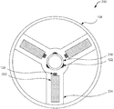
도 2는 그립핑 컴포넌트, 자석, 및 검출 센서를 포함하는 회전 메커니즘의 일 실시예의 저면도를 도시한다.
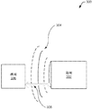
도 3은 마이크로 전자 기판의 위치를 검출하기 위해 프로세스 시스템에 의해 사용되는 검출 센서 및 자성 컴포넌트의 개략도를 도시한다.
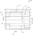
도 4는 회전 메커니즘이 풀릴 수 있는 때를 결정하는 방법의 일 실시예를 도시하는 그래프를 도시한다.
도 5는 마이크로 전자 기판이 회전 메커니즘에 고정되는지 여부를 검출하는 하나의 방법에 대한 흐름도를 도시한다.BRIEF DESCRIPTION OF THE DRAWINGS The accompanying drawings, which are incorporated in and constitute a part of this specification, illustrate embodiments of the invention and, together with the general description given above and the detailed description given below, serve to explain the invention. Additionally, the number (s) to the left of the reference number identifies the drawing in which the reference number first appears.
Figure 1 shows a schematic diagram of a process system that may include a rotation mechanism and a microelectronic substrate position detection system.
Figure 2 shows a bottom view of one embodiment of a rotating mechanism including a gripping component, a magnet, and a detection sensor.
Figure 3 shows a schematic diagram of a detection sensor and a magnetic component used by a process system to detect the position of a microelectronic substrate.
Figure 4 shows a graph illustrating one embodiment of a method for determining when a rotation mechanism can be released.
Figure 5 shows a flow diagram of one method for detecting whether a microelectronic substrate is secured to a rotation mechanism.
기판으로부터 물질을 선택적으로 제거하기 위한 방법이 다양한 실시예들에서 설명되어 있다. 당업자는 다양한 실시예들이 특정한 세부 사항들 중 하나 이상 없이 실시되거나, 또는 다른 대체 및/또는 추가적인 방법, 물질, 또는 컴포넌트로 실시될 수 있다는 것을 인식할 것이다. 다른 경우에, 잘 공지된 구조물들, 물질들, 또는 동작들은 본 발명의 다양한 실시예들의 양태들을 모호하게 하는 것을 피하기 위해서 상세하게 도시되거나 기술되지 않는다. 유사하게, 설명을 위해, 특정 번호, 물질들, 및 구성들이 본 발명의 철저한 이해를 제공하기 위해 기재되어 있다. 그럼에도 불구하고, 본 발명은 특정한 세부 사항 없이 실시될 수 있다. 더욱이, 도면들에 도시된 다양한 실시예들은 예시적인 표현이며, 반드시 실척도로 도시되는 것은 아님을 이해한다.A method for selectively removing material from a substrate is described in various embodiments. Those skilled in the art will recognize that the various embodiments may be practiced without one or more of the specific details, or may be practiced with other alternative and / or additional methods, materials, or components. In other instances, well-known structures, materials, or operations are not shown or described in detail in order to avoid obscuring aspects of various embodiments of the present invention. Similarly, for purposes of explanation, certain numbers, materials, and configurations are set forth in order to provide a thorough understanding of the present invention. Nevertheless, the present invention may be practiced without specific details. Moreover, it is understood that the various embodiments shown in the figures are exemplary representations and are not necessarily drawn to scale.
본 명세서 전반에 걸쳐, "일 실시예" 또는 "실시예"에 대한 참조는 실시예와 관련되어 설명된 특정한 특징, 구조물, 물질, 또는 특성이 본 발명의 적어도 하나의 실시예에 포함되지만, 이들이 모든 실시예에 존재한다는 것을 나타내는 것이 아님을 의미한다. 따라서, 본 명세서 전반에 걸쳐 다양한 장소에서 "일 실시예에서" 또는 "실시예에서" 구절의 출현은 반드시 본 발명의 동일한 실시예를 나타내는 것은 아니다. 더욱이, 특정한 특징, 구조물, 물질, 또는 특성은 하나 이상의 실시예들에서 임의의 적합한 방식으로 결합될 수 있다. 다양한 부가적인 층들 및/또는 구조물들이 포함될 수 있고 및/또는 설명된 피처들은 다른 실시예들에서 생략될 수 있다.Reference throughout this specification to "one embodiment" or "an embodiment" means that a particular feature, structure, material, or characteristic described in connection with the embodiment is included in at least one embodiment of the invention, But does not indicate that it is present in all embodiments. Thus, the appearances of the phrase " in one embodiment "or" in an embodiment "in various places throughout this specification are not necessarily indicative of the same embodiment of the present invention. Moreover, a particular feature, structure, material, or characteristic may be combined in any suitable manner in one or more embodiments. Various additional layers and / or structures may be included and / or the described features may be omitted in other embodiments.
본 명세서에서 사용되는 "마이크로 전자 기판"은 일반적으로 본 발명에 따라 처리되는 대상을 지칭한다. 마이크로 전자 기판은 디바이스, 특히 반도체 또는 다른 전자 디바이스의 임의의 물질 부분 또는 구조물을 포함할 수 있으며, 예를 들어, 반도체 기판과 같은 베이스 기판 구조물 또는 박막과 같은 베이스 기판 구조물 상의 또는 그 위의 층일 수 있다. 따라서, 기판은 임의의 특정한 베이스 구조물, 밑에 있는 층 또는 위에 있는 층, 패턴화 또는 비패턴화로 제한되지 않고, 오히려 이러한 층 또는 베이스 구조물, 및 층 및/또는 베이스 구조물의 임의의 조합을 포함하는 것으로 고려된다. 이하의 설명은 특정 타입의 기판을 참조할 수 있지만, 이것은 단지 예시를 위한 것으로 제한하기 위한 것이 아니다. 마이크로 전자 기판 이외에, 본 명세서에 기재된 기술은 또한 포토 리소그래피 기술을 사용하여 마이크로 전자 기판의 패턴화에 사용될 수 있는 레티클 기판을 세정하기 위해 사용될 수 있다.As used herein, a "microelectronic substrate" generally refers to an object to be processed in accordance with the present invention. A microelectronic substrate may comprise any material or portion of a device, particularly a semiconductor or other electronic device, and may be a base substrate structure, such as, for example, a semiconductor substrate, or a layer on or above a base substrate structure, have. Thus, the substrate is not limited to any particular base structure, underlying or overlying layer, patterned or unpatterned, but rather includes any such combination of layers or base structures and layers and / or base structures . The following description may refer to a particular type of substrate, but is not intended to be limiting for the sake of illustration only. In addition to microelectronic substrates, the techniques described herein can also be used to clean a reticle substrate that can be used for patterning microelectronic substrates using photolithographic techniques.
이제 도면을 참조하면, 도 1은 마이크로 전자 기판(도시되지 않음)을 처리하기 위해 사용될 수 있는 대표적인 시스템(100)의 개략도, 및 프로세스 챔버(106)에서의 처리 동안 마이크로 전자 기판을 고정하기 위해 사용되는 회전 척(104)의 일 실시예의 단면도(102)를 제공한다. 일 실시예에서, 프로세스 챔버(106) 처리는 마이크로 전자 기판의 처리를 가능하게 하거나 향상시키기 위해서 마이크로 전자 기판의 회전을 포함할 수 있다. 처리는 프로세스 챔버(106)에서 마이크로 전자 기판에 노출되는 가스 및/또는 화학 물질(chemical)을 포함할 수 있지만, 이에 제한되는 것은 아니다. 처리를 가능하게 하기 위해, 시스템(100)은 다양한 조건(예를 들어, 온도, 압력, 시간 등) 하에 마이크로 전자 기판에 노출될 수 있는 다양한 화학적 유체(예를 들어, 기상, 액상, 또는 이들의 조합)를 제공할 수 있는 하나 이상의 유체 전달 시스템들(108)을 포함할 수 있지만, 이에 제한되는 것은 아니다. 화학적 프로세싱 분야의 당업자에 의해 이해되는 바와 같이, 유체 전달 시스템(108)은 프로세스 챔버(106)에 전달되는 화학적 유체의 흐름, 농도 및/또는 온도를 제어할 수 있는 파이핑 및 다양한 제어 메커니즘을 포함할 수 있다. 또한, 시스템(100)은 화학적 유체 또는 처리 부산물을 프로세스 챔버(106)로부터 제거할 수 있는 배기 시스템(110)을 포함할 수 있다. 당업자에 의해 이해되는 바와 같이, 배기 시스템은 특정 방향으로 가스 또는 액체의 흐름을 가능하게 하는 압력차 시스템을 사용하여 가스 및/또는 액체를 제거하는 다양한 기술을 포함할 수 있다. 배기 시스템(110)은 또한 당업계에 공지된 기술을 사용하여 프로세스 챔버(106)로부터의 화학 물질 제거율을 제어할 수 있다.Referring now to the drawings, FIG. 1 is a schematic diagram of an
시스템(100)은 또한 마이크로 전자 기판을 프로세스 챔버(106) 안팎으로 이동시키는 동작, 및 처리에 사용되는 화학 물질의 전달 및 제거를 제어 또는 관리할 수 있는 제어기(112)를 포함할 수 있다. 제어기(112)의 일 양태는 처리 이전에, 처리 동안에 및/또는 처리 이후에 마이크로 전자 기판의 움직임을 모니터링하는 것이다. 예를 들어, 하나의 처리 조건은 화학 물질이 프로세스 챔버(106)에 존재할 때 마이크로 전자 기판을 회전시키는 것을 포함할 수 있다. 그러나, 처리 이전에, 처리 동안에 및/또는 처리 이후에 마이크로 전자 기판이 회전 척(104)에 고정되어 있다는 것을 확인하는 것이 바람직할 수 있다. 제어기(112)는 메모리(116)에 저장될 수 있는 검출 컴포넌트(114)에 전기 신호를 제공할 수 있는 회전 척(104)에 통합된 검출 시스템과 상호 작용할 수 있다. 도 1에 도시된 바와 같이, 제어기(112)는 통신 네트워크(120)(예를 들어, 점선)를 통해 시스템(100)의 컴포넌트들과 전기적으로 통신할 수 있다.The
이 실시예에서, 검출 컴포넌트(114)는 마이크로 전자 기판이 회전 척(104)에 제대로 고정되었음을 전기 신호가 나타내는지 여부를 결정하기 위해 컴퓨터 프로세서(118) 상에서 실행될 수 있는 컴퓨터 실행 가능 명령어들을 포함할 수 있다. 유사한 방식으로, 프로세스 컴포넌트(120)는 유체 전달 시스템(108) 및 배기 시스템(110)을 제어 또는 동작시키는 컴퓨터 실행 가능 명령어들을 포함할 수 있다.In this embodiment, the detection component 114 includes computer-executable instructions that may be executed on the
마이크로 전자 기판이 제대로 고정되었음을 나타내는, 검출 컴포넌트(114)에 제공된 전기 신호(도시되지 않음)는 회전 척(104)의 일부 양태를 모니터링할 수 있는 검출 센서(122)에 의해 제공될 수 있다. 도 1의 실시예에서, 마이크로 전자 기판은 마이크로 전자 기판을 회전 척(104)에 고정시키는 압력을 가하기 위해 피봇 조인트(128)를 사용하여 기계적 디바이스(126)(예를 들어, 스프링)에 의해 작동될 수 있는 그립핑 메커니즘(124)을 포함할 수 있다. 이 경우, 그립핑 메커니즘(124)은 양방향 화살표로 표시된 바와 같이 측 방향으로 움직일 수 있다. 마이크로 전자 기판이 제대로 고정되었음을 나타내는 하나의 표시는 그립핑 메커니즘(124)의 위치이다. 위치는 그립핑 메커니즘(124)과 함께 움직일 수 있는 위치 지시기(128)(예를 들어, 자석)를 사용함으로써 모니터링될 수 있다. 예를 들어, 마이크로 전자 기판이 회전 척(104)으로부터 손실되거나 제거될 때, 그립핑 메커니즘(124)은 기계적 디바이스(126)에 대한 반대 저항의 손실로 인해 움직일 수 있다. 검출 센서(122)는 그 움직임을 검출하고, 검출 컴포넌트(114)에 의해 해석될 수 있는 전기 신호를 생성하여, 마이크로 전자 기판이 제대로 고정되지 않았음을 결정할 수 있다. 따라서, 제어기(112)는 느슨한 마이크로 전자 기판에 의해 야기되는 프로세스 챔버(102)에 대한 추가적인 손상을 방지하기 위해 회전 척(104)에게 회전을 정지시키도록 지시할 수 있다.An electrical signal (not shown) provided to the sensing component 114, which indicates that the microelectronic substrate is properly secured, may be provided by a
위치 지시기(128)는 검출 센서(122)에 의해 관측 가능하고, 그립핑 메커니즘(124)이 움직였다는 표시 또는 마이크로 전자 기판이 더 이상 회전 척(104)에 고정되어 있지 않다는 표시를 제공할 수 있는 임의의 컴포넌트를 포함할 수 있다. 일 실시예에서, 위치 지시기(128)는 자석일 수 있으며, 이 자석은 자석에 걸쳐 크기가 변하거나 자석으로부터 멀리 떨어져 있을 수 있는 자기장을 방출할 수 있다. 검출 센서(122)는 자기장 강도의 변화를 검출할 수 있고, 자기장 강도를 나타낼 수 있는 전기 신호를 생성할 수 있다. 일 예에서, 검출 센서(122)는 자기장 검출에 응답하여 전압을 생성할 수 있는 홀 효과 센서를 포함할 수 있다. 전압 크기는 자기장 강도의 크기에 따라 변할 수 있다. 예를 들어, 자석 타입에 따라, 더 높은 전계 강도는 더 높은 전압을 생성할 수 있고, 더 낮은 전계 강도는 더 낮은 전압을 생성할 수 있다. 따라서, 위치 지시기(128)의 위치는 홀 효과 센서에 의해 검출된 전계 강도로 어림잡거나, 전계 강도와 상관될 수 있다. 최소한, 자기장 강도의 변화는 위치 지시기(128)의 위치가 움직였다는 것을 나타낼 수 있고, 이는 그립핑 메커니즘(124)이 움직였다는 것을 나타낸다. 움직임은 마이크로 전자 기판이 더 이상 회전 척(104)에 제대로 고정되지 않아서 일 수 있다.The
자석과 자성 센서 사이의 상호 작용은 도 3의 설명에서 보다 상세히 기술될 것이다. 검출 컴포넌트(114) 및 검출 센서(122)의 동작을 설명하는 일 실시예가 도 4 및 도 5의 설명에서 보다 상세히 기술될 것이다.The interaction between the magnet and the magnetic sensor will be described in more detail in the description of FIG. One embodiment for explaining the operation of the detection component 114 and the
도 2는 검출 센서(122)와 위치 지시기(128)의 조합을 포함할 수 있는 저면도(200)로부터 회전 척(104)의 일 실시예를 도시한다. 검출 센서(122)와 위치 지시기(128)의 세 개의 쌍이 있지만, 쌍의 총수는 변할 수 있고, 검출 센서(122)와 위치 지시기(128) 간의 페어링(pairing)은 필요하지 않다. 예를 들어, 다수의 위치 지시기(128)가 단일 위치 검출기(122)와 함께 사용될 수 있고, 그 반대도 가능하다.Figure 2 illustrates one embodiment of a
도 2 실시예에서, 회전 척(104)은 마이크로 전자 기판(도시되지 않음)을 고정하기 위해 압력을 가할 수 있는 각각의 작동 메커니즘(202)에 결합된 세 개의 그립핑 메커니즘(도시되지 않음)을 포함할 수 있다. 작동 메커니즘(202)은 지지 또는 레버리지를 제공할 수 있는 각각의 장착 암(204)에 고정될 수 있어, 위치 지시기(128)는 장착 암에 대해 수직 방향, 수평 방향, 또는 이 둘의 조합으로 움직일 수 있다. 예를 들어, 장착 암(202)이 마이크로 전자 기판을 고정하도록 배치될 수 있기 때문에, 위치 지시기(128)는 검출 센서(122)의 알려진 거리 내에 배치될 수 있다. 이러한 방식으로, 검출 센서(122)는 검출 컴포넌트(114)를 사용하여 위치를 식별하기 위해 사용될 수 있는 전기 신호를 검출하고 생성할 수 있다. 위치 지시기(128)가 중심 어셈블리(206) 주위를 회전함에 따라, 고정 검출 센서(128)는 위치 지시기(128) 옆을 지나면서 위치 지시기(128) 각각에 대한 전기 신호를 생성하여, 그 위치를 나타내는 관측 가능 신호를 제공할 수 있다. 자석 실시예에서, 관측 가능 신호는 홀 효과 센서(예를 들어, 검출 센서(122))에 의해 검출될 수 있는 자기장일 수 있다. 그러나, 다른 실시예들에서, 관측 가능 신호는 광, 전압, 전력, 전류, 열, 또는 이들의 조합을 포함할 수 있다. 검출 센서(122) 및 위치 지시기(128)는 제어기(112)에 제공될 수 있는 관측 가능 신호를 생성 및/또는 검출하도록 적절하게 구성될 수 있다.2 embodiment, the
도 3은 회전 척(104)(도시되지 않음)에 대하여 마이크로 전자 기판(도시되지 않음)의 위치를 검출하기 위해 프로세스 시스템(100)에 의해 사용되는 검출 센서(122)(예를 들어, 홀 효과 센서) 및 위치 지시기(128)(예컨대, 자석)의 개략도를 도시한다.Figure 3 illustrates a
이 실시예에서, 자석(302)은 홀 효과 센서(306)에 의해 검출될 수 있는 자기장(304)을 방출할 수 있다. 자기장(304)의 전계 강도는 거리에 따라 변할 수 있어서, 자석(302)과 홀 효과 센서(306) 사이의 상대 위치(308)는 전계 강도의 크기와 상관될 수 있다. 홀 효과 센서(306)는 상대 위치(308)를 나타낼 수 있는 전압 또는 전기 신호를 생성할 수 있다. 상대 위치(308)가 수평 거리로 도시되어 있지만, 상대 위치는 x, y, 및 z 방향 내에서 변경될 수 있다. 홀 효과 센서(306)가 자석(302)으로부터 방출된 자기장(예를 들어, 관측 가능 신호)을 검출할 수 있게 하는 임의의 방식에서 위치는 변경될 수 있다. 검출 컴포넌트(114)는 자기장의 임의의 부분을 마이크로 전자 기판이 회전 척(104)에 의해 안전하게 유지되었다는 것을 나타내는 크기와 상관시키도록 구성될 수 있다.In this embodiment, the magnet 302 is capable of emitting a
일 실시예에서, 자석(302)은 극성이 변할 수 있어, 홀 효과 센서(306)에 의해 검출된 자기장은 두 가지 상이한 타입의 전기 신호들이 생성되어 검출 컴포넌트(114)에 제공될 수 있도록 할 수 있다. 이 실시예의 일례가 도 4의 설명에서 설명될 것이다.In one embodiment, the magnet 302 can be polarized so that the magnetic field detected by the Hall effect sensor 306 can be generated so that two different types of electrical signals can be generated and provided to the detection component 114 have. An example of this embodiment will be explained in the description of Fig.
다른 실시예들에서, 관측 가능 신호는 자기장이 아닐 수 있다. 예를 들어, 광이 위치 지시기(128)에 의해 발산되거나 이로부터 압력이 가해질 수 있고, 적절한 검출 센서(122)에 의해 검출될 수 있다. 예를 들어, 광의 세기는 광 센서(도시되지 않음)에 의해 검출될 수 있고, 압력 변환기(도시되지 않음)가 압력의 변화를 검출하기 위해 사용될 수 있다. 그러나, 검출 컴포넌트(114)는 관측 가능 신호를 그립핑 메커니즘(124)의 위치와 상관시키고, 마이크로 전자 기판이 회전 척(104)에 의해 제대로 고정되었는지 여부를 결정하도록 구성될 수 있다.In other embodiments, the observable signal may not be a magnetic field. For example, light may be diverted or exerted by the
도 4는 검출 센서(122)로부터 검출 컴포넌트(114)에 의해 수신된 신호에 적어도 부분적으로 기초하여 회전 척(104)이 회전을 정지시킬 때를 결정하는 방법의 일 실시예를 나타내는 그래프(400)를 포함한다. 대체로, 검출 컴포넌트(122)는 검출 센서(들)(122)로부터의 신호를 모니터링할 수 있고, 이들을 하나 이상의 문턱값 레벨들(예를 들어, 남극 극성 문턱값(402), 북극 극성 문턱값(404))과 비교할 수 있다.4 is a
상이한 문턱값 레벨들은 상이한 극성을 갖는 자석들과 연관될 수 있다. 일 실시예에서, 회전 척(104)은 상이한 관측 가능 특성들을 포함할 수 있는 복수의 위치 지시기들(128)을 포함할 수 있다. 예를 들어, 위치 지시기들(128)은 그립핑 메커니즘(124)의 동일한 위치에 상관될 수 있는 상이한 전기 신호들을 초래할 수 있는 상이한 극성들(예를 들어, 북극 또는 남극)을 갖는 자석들을 포함할 수 있지만, 이에 제한되는 것은 아니다. 전기 신호는 회전 척(104)을 정지시킬지 여부를 결정하기 위해 검출 컴포넌트(114)에 의해 단독으로 또는 조합하여 사용될 수 있다.The different threshold levels may be associated with magnets having different polarities. In one embodiment, the
그래프(400)는 신호 강도(예를 들어, 신호 축(406)), 회전 척(104)의 분당 회전 수(예를 들어, rpm 축(408)), 및 시간(예를 들어, 시간 축(410))과 관련된 정보의 조합을 포함한다. 시간은 시간 축(410)을 따라 좌측에서부터 우측으로 증가하고, 그래프(400)는 회전 척(104)이 rpm 플롯 당 1000rpm으로 회전하는 중간 처리 중에 시작된다(412). 남극 자석(414)에 대한 신호 강도(예를 들어, 검출 센서(122))는 180 바로 아래에서 시작하고, 북극 자석(416)에 대한 신호 강도(예를 들어, 검출 센서(122))는 약 80에서 시작한다. 전술한 바와 같이, 신호 강도는 자석(302)으로부터의 관측 가능 신호(예를 들어, 자기장(304))와 상관되는 전압을 생성하는 홀 효과 센서(306)에 의해 생성될 수 있다. 그래프(400)에 도시된 크기는 설명을 위한 것으로, 신호 축(406), rpm 축(408), 또는 시간 축(410) 상의 값으로 청구항의 범위를 제한하려는 것은 아니다.The
도 4의 실시예에서, 검출 컴포넌트(114)는 남극 자석(414) 신호 및 북극 자석(416) 신호를 모니터링할 수 있다. 검출 컴포넌트(114)는 신호들을, 신호들 각각의 문턱값들과 비교할 수 있다. 예를 들어, 남극 자석 신호가 약 240으로 증가하고 남극 극성 문턱값(402)을 교차할 때, 검출 컴포넌트(114)는 마이크로 전자 기판이 고정되지 않은 것으로 결정하고, 회전 척(104)이 회전을 정지시키도록 지시할 수 있다. 램프 다운으로의 전이는 0rpm으로 끝나는 램프다운 포인트(412)에 도시되어 있다. 다른 실시예에서, 검출 컴포넌트(114)는 마이크로 전자 기판이 고정되지 않았음을 결정하기 위해 북극 자석(416) 신호를 사용할 수 있다. 도 4에 도시된 바와 같이, 북극 자석(416) 신호는 북극 극성 문턱값 레벨(404)을 교차할 수 있고, 검출 컴포넌트(114)는 회전 척(104)이 회전을 정지시키도록 지시할 수 있다. 또 다른 실시예에서, 검출 컴포넌트(114)는 마이크로 전자 기판이 제대로 고정되지 않았음을 결정하기 위해 남극 자석(414) 신호와 북극 자석(416) 신호 모두를 조합하여 사용할 수 있다. 이 경우, 남극 자석(414) 신호 및 북극 자석(416) 신호 모두는 검출 컴포넌트(114)가 회전 척(104)을 정지시키기 전에 각각의 문턱값 레벨을 교차해야 한다.In the embodiment of FIG. 4, the detection component 114 may monitor the
문턱값 레벨들(예를 들어, 남극 극성 문턱값(402) 등)은 그립핑 메커니즘(124)의 실험 또는 교시를 통해 결정될 수 있다. 이러한 방식으로, 문턱값 레벨들은 마이크로 전자 기판을 회전 척(104)으로 그립핑하고, 검출 컴포넌트에 그립 설정 포인트를 설정함으로써 결정될 수 있다. 그 다음, 마이크로 전자 기판이 느슨해질 때까지 마이크로 전자 기판을 천천히 풀고, 검출 컴포넌트(114)에서 홀 효과 센서(306)로부터의 전압을 도 4에 도시된 바와 같이 처리 동안 회전 척(104)의 정지를 트리거하는 문턱값 레벨로서 설정한다.Threshold levels (e.g.,
다른 실시예에서, 문턱값 레벨들은 입력 자석 신호들의 백분율 변화와 같은 설정 편차량에 기초할 수 있다. 예를 들어, 신호의 크기가 10% 또는 20% 이상 벗어나면, 검출 컴포넌트(114)는 마이크로 전자 기판이 제대로 고정되지 않았음을 결정할 수 있고, 회전 척(104)을 정지시킬 수 있다. 다른 실시예들에서, 신호는 이상치 이벤트(outlier event)(예를 들어, 예상하지 못한 신호 피크)의 영향을 줄이기 위해, 그리고 오정지(false shutdown)를 방지함으로써 회전 척(104)의 더욱 양호한 제어를 제공하기 위해 정규화될 수 있다.In another embodiment, the threshold levels may be based on a setting deviation vehicle such as a percentage change in the input magnet signals. For example, if the magnitude of the signal deviates by more than 10% or 20%, the detection component 114 can determine that the microelectronic substrate is not properly secured and can stop the
도 5는 마이크로 전자 기판이 회전 척(104)에 고정되었는지 여부를 검출하고 마이크로 전자 기판이 손실되거나 고정되지 않은 것으로 결정될 때 회전을 정지시키는 한 방법에 대한 흐름도(500)를 도시한다. 전술한 바와 같이, 제어기(112)는 회전 척(104) 및 이의 그립핑 메커니즘(124)을 제어하기 위해 사용될 수 있다. 제어기(112)는 또한 마이크로 전자 기판이 회전 척(104)에 제대로 고정되었는지 여부를 결정할 수 있다. 이 실시예를 구현하는 한 방법이 흐름도(500)에서 설명된다.Figure 5 shows a flow diagram 500 of a method for detecting whether a microelectronic substrate is fixed to a
블록(502)에서, 시스템(100)은 마이크로 전자 기판을 운송 카세트로부터 프로세스 챔버(106)로 이송할 수 있는 핸들링 메커니즘을 포함할 수 있다. 핸들링 메커니즘은 마이크로 전자 기판을 회전 척(104) 상에 배치할 수 있고, 제어기(112)는 마이크로 전자 기판을 처리하기 전에 그립핑 메커니즘(124)을 작동시킬 수 있다.At
일 실시예에서, 회전 척(104)은 그립핑 메커니즘(124)에 결합될 수 있는 위치 지시기(128)를 포함할 수 있다. 위치 지시기(128)는 마이크로 전자 기판이 회전 척(104)에 고정되었음을 나타내는 특정 방식으로 배치될 수 있다. 예를 들어, 그립핑 메커니즘(124)은 개방 위치로부터 폐쇄 위치로 이동할 수 있다. 개방 위치와 폐쇄 위치 간의 이동은 또한 검출 센서(122)에 관련된 위치 지시기(128)를 이동시킬 수 있다. 제어기(112)는 마이크로 전자 기판이 제대로 고정되었는지 여부를 나타내는 것으로 해석될 수 있는 신호를 검출 센서로부터 수신할 수 있다.In one embodiment, the
블록(504)에서, 제어기(112)는 마이크로 전자 기판이 그립핑 메커니즘(124)에 의해 제대로 고정된 것으로 검출 컴포넌트(114)가 결정할 때 회전 척이 회전하도록 지시할 수 있다. 전술한 바와 같이, 검출 컴포넌트(114)는 검출 센서(122)로부터의 신호를 메모리(116)에 저장된 값 또는 시그니처와 비교할 수 있다.At block 504, the controller 112 may direct the rotating chuck to rotate when the detecting component 114 determines that the microelectronic substrate is properly secured by the
블록(506)에서, 검출 센서(122)는 마이크로 전자 기판의 처리 중에 회전 척(124)이 회전할 때 위치 지시기(128)의 위치 또는 위치 지시기(128)로부터의 신호를 계속 검출할 수 있다.At
일 실시예에서, 위치 지시기(128)는 그립핑 메커니즘(124)이 작동되어 마이크로 전자 기판을 고정할 때, 움직이거나 배치될 수 있는 하나 이상의 자석들을 포함할 수 있다. 자석(들)은 자화된 강자성 물질(예를 들어, 철, 니켈)로 구성될 수 있으며, 자석으로부터 방출된 자기장의 방향을 나타낼 수 있는 남극 또는 북극의 극성을 가질 수 있다. 자기장은 검출 센서(122)에 관련된 자석의 위치를 나타낼 수 있는 거리 또는 위치 의존 시그니처를 가질 수 있다. 예를 들어, 자기장은 환경에 미치는 영향을 기반으로 하여 특징지어질 수 있다. 일 실시예에서, 자기장은 이동하는 하전 입자 상에 가해지는 힘으로서 특징지어질 수 있어서, 자기장은 전자의 움직임을 유도하고 다른 비접촉 대상 내에서 전류 흐름을 생성할 수 있다. 전류 흐름의 크기는 자기장의 강도를 나타낼 수 있고, 이는 비접촉 대상으로부터의 거리를 결정하기 위해 사용될 수 있다. 이러한 방식으로, 전류 흐름은 자석의 위치를 어림잡기 위해 사용될 수 있다. 예를 들어, 그립핑 메커니즘(124) 위치는 근접한 자기장에 의해 검출 센서(122)에서 생성된 전류에 기초하여 추론될 수 있다.In one embodiment, the
블록(508)에서, 제어기(112)는 회전 척(104)이 회전하는 동안, 위치 지시기(128)에 근접할 수 있는 적어도 하나의 검출 컴포넌트(122)로부터 신호를 수신할 수 있다. 신호는 자석(들)으로부터의 자기장 강도를 반영할 수 있어, 그립핑 메커니즘(124)의 위치를 어림잡을 수 있다. 근사는 마이크로 전자 기판이 회전 척(104)에 단단히 연결되었는지 여부를 추론할 수 있어, 마이크로 전자 기판이 회전 척(104)과 거의 동일한 속도로 회전하고 및/또는 유체 전달 시스템(108) 포트 또는 유입구에 대해 안정한 x-y-z 위치를 유지한다.At
이 실시예에서, 신호는 제대로 고정된 마이크로 전자 기판과 연관될 수 있는 제 1 시그니처를 가질 수 있다. 제어기(112)는 이 제 1 시그니처 신호가 검출 컴포넌트(114)에 의해 검출되거나 분석될 때 회전 척(104)을 계속 회전시킬 수 있다. 그러나, 제어기(112)는 제 1 시그니처 신호가 제 2 시그니처 신호로 대체될 때 대응하거나 조치를 취할 수 있다. In this embodiment, the signal may have a first signature that may be associated with a properly fixed microelectronic substrate. The controller 112 may continue to rotate the
블럭(510)에서, 제어기(112)는 제 2 시그니처 신호가 검출될 때 회전 척(104)의 회전 속도를 감소시킬 수 있다. 일 실시예에서, 제 2 시그니처 신호는 마이크로 전자 기판이 회전 척(104)에 의해 더 이상 제대로 고정되지 않을 수 있다는 것을 나타내는 문턱값을 초과하거나 그보다 낮은 임의의 값일 수 있다. 문턱값들과 신호(들) 사이의 상호 작용은 도 4의 설명에서 상술되어 있다.At
비록 본 발명의 특정 실시예들만이 상세하게 상술되었지만, 당업자는 본 발명의 신규한 교지 및 이점으로부터 실질적으로 벗어나지 않고 실시예들에서 많은 변형이 가능하다는 것을 용이하게게 인식할 것이다. 따라서, 이와 같은 모든 변형은 본 발명의 범위 내에 포함되는 것으로 의도된다.Although only certain embodiments of the invention have been described in detail, those skilled in the art will readily appreciate that many modifications are possible in the embodiments without materially departing from the novel teachings and advantages of this invention. Accordingly, all such modifications are intended to be included within the scope of the present invention.
Claims (20)
화학적 프로세싱 시스템에서 적어도 하나의 위치 지시기 컴포넌트 및 적어도 하나의 검출 컴포넌트를 포함하는 회전 척에 상기 마이크로 전자 기판을 결합시키는 단계;
상기 회전 척을 사용하여 상기 마이크로 전자 기판을 회전시키는 단계;
상기 검출 컴포넌트를 사용하여, 상기 검출 컴포넌트에 관련된 상기 적어도 하나의 위치 지시기 컴포넌트의 위치를 검출하는 단계;
상기 적어도 하나의 검출 컴포넌트로부터 신호를 수신하는 단계; 및
상기 신호가 문턱값을 초과하거나 문턱값보다 낮은 경우, 상기 회전 척의 회전 속도를 감소시키는 단계
를 포함하는 마이크로 전자 기판을 처리하기 위한 방법.A method for processing a microelectronic substrate,
Coupling the microelectronic substrate to a rotating chuck comprising at least one position indicator component and at least one sensing component in a chemical processing system;
Rotating the microelectronic substrate using the rotating chuck;
Using the detection component, detecting a position of the at least one position indicator component associated with the detection component;
Receiving a signal from the at least one detection component; And
Decreasing a rotational speed of the rotary chuck when the signal exceeds a threshold or is lower than a threshold,
≪ / RTI >
마이크로 전자 기판을 처리하기 위한 프로세스 챔버;
상기 프로세스 챔버 내의 회전 척으로서, 상기 회전 척은 위치 지시기 컴포넌트들 및 검출 컴포넌트들을 포함하는 것인, 상기 회전 척; 및
상기 검출 컴포넌트들로부터 신호들을 수신할 수 있고, 상기 신호들이 문턱값을 초과하면 상기 회전 척을 정지시킬 수 있는 제어기
를 포함하는 시스템.In the system,
A process chamber for processing a microelectronic substrate;
A rotating chuck in the process chamber, wherein the rotating chuck comprises position indicator components and detection components; And
A controller able to receive signals from the detection components and to stop the rotary chuck when the signals exceed a threshold,
/ RTI >
상기 프로세스 챔버에 적어도 하나의 화학 물질(chemical)을 제공하는 유체 전달 시스템; 및
상기 프로세스 챔버로부터 상기 적어도 하나의 화학 물질을 제거할 수 있는 배기 시스템
을 더 포함하는 시스템.11. The method of claim 10,
A fluid delivery system for providing at least one chemical to the process chamber; And
An exhaust system capable of removing said at least one chemical from said process chamber
≪ / RTI >
회전 척을 사용하여 마이크로 전자 기판을 회전시키는 단계;
검출 컴포넌트를 사용하여, 상기 검출 컴포넌트에 관련된 적어도 하나의 위치 지시기 컴포넌트의 위치를 검출하는 단계;
적어도 하나의 상기 검출 컴포넌트로부터 신호를 수신하는 단계; 및
상기 신호가 문턱값을 초과하거나 문턱값보다 낮은 경우, 상기 회전 척의 회전 속도를 감소시키는 단계
를 포함하는 방법을 구현할 수 있는 것인, 하나 이상의 텐저블 비일시적 컴퓨터 판독 가능 매체.Readable medium having computer executable instructions that, when executed by a computer processor, cause the processor to perform the steps of:
Rotating the microelectronic substrate using a rotating chuck;
Using the detection component, detecting a position of at least one position indicator component associated with the detection component;
Receiving a signal from at least one said sensing component; And
Decreasing a rotational speed of the rotary chuck when the signal exceeds a threshold or is lower than a threshold,
Wherein the computer program product is capable of implementing a method comprising:
Applications Claiming Priority (1)
| Application Number | Priority Date | Filing Date | Title |
|---|---|---|---|
| PCT/US2014/069557 WO2016093824A1 (en) | 2014-12-10 | 2014-12-10 | Detection of lost wafer from spinning chuck |
Publications (1)
| Publication Number | Publication Date |
|---|---|
| KR20170093949A true KR20170093949A (en) | 2017-08-16 |
Family
ID=56107842
Family Applications (1)
| Application Number | Title | Priority Date | Filing Date |
|---|---|---|---|
| KR1020177019065A KR20170093949A (en) | 2014-12-10 | 2014-12-10 | Detection of lost wafer from spinning chuck |
Country Status (4)
| Country | Link |
|---|---|
| JP (1) | JP2018501654A (en) |
| KR (1) | KR20170093949A (en) |
| CN (1) | CN107112257A (en) |
| WO (1) | WO2016093824A1 (en) |
Family Cites Families (10)
| Publication number | Priority date | Publication date | Assignee | Title |
|---|---|---|---|---|
| US3538883A (en) * | 1967-12-12 | 1970-11-10 | Alco Standard Corp | Vacuum chuck with safety device |
| JP2529637Y2 (en) * | 1991-08-30 | 1997-03-19 | 大日本スクリーン製造株式会社 | Substrate rotation holding device |
| DE4237928C2 (en) * | 1992-07-09 | 1995-01-19 | Siemens Ag | Microswitch with a magnetic field sensor |
| US6459382B1 (en) * | 2001-04-26 | 2002-10-01 | Applied Materials, Inc. | Over clamp sensor |
| US6670807B2 (en) * | 2002-01-16 | 2003-12-30 | Applied Materials, Inc. | Proximity sensor detecting loss of magnetic field complete |
| KR100460807B1 (en) * | 2002-07-08 | 2004-12-09 | 삼성전자주식회사 | wafer shape inspection equipment of semiconductor devise manufacturing equipment, cleaning equipment the using and inspection method there of |
| JP5379533B2 (en) * | 2009-03-27 | 2013-12-25 | 大日本スクリーン製造株式会社 | Substrate holding mechanism and substrate processing apparatus provided with the substrate holding mechanism |
| JP5646528B2 (en) * | 2012-03-09 | 2014-12-24 | 東京エレクトロン株式会社 | Liquid processing equipment |
| CN102867771B (en) * | 2012-09-18 | 2015-08-05 | 北京七星华创电子股份有限公司 | There is clamping device and the method for monitoring semiconductor wafer status function |
| US9255894B2 (en) * | 2012-11-09 | 2016-02-09 | Kla-Tencor Corporation | System and method for detecting cracks in a wafer |
-
2014
- 2014-12-10 KR KR1020177019065A patent/KR20170093949A/en not_active Application Discontinuation
- 2014-12-10 JP JP2017531335A patent/JP2018501654A/en not_active Ceased
- 2014-12-10 CN CN201480084511.4A patent/CN107112257A/en active Pending
- 2014-12-10 WO PCT/US2014/069557 patent/WO2016093824A1/en active Application Filing
Also Published As
| Publication number | Publication date |
|---|---|
| WO2016093824A1 (en) | 2016-06-16 |
| JP2018501654A (en) | 2018-01-18 |
| CN107112257A (en) | 2017-08-29 |
Similar Documents
| Publication | Publication Date | Title |
|---|---|---|
| US9564378B2 (en) | Detection of lost wafer from spinning chuck | |
| JP5387921B2 (en) | Electrostatic chuck device and method for determining adsorption state of substrate | |
| CN101479611B (en) | Methods and apparatus for sensing unconfinement in a plasma processing chamber | |
| US20150270146A1 (en) | Substrate processing apparatus and substrate processing method | |
| TWI259548B (en) | Proximity sensor | |
| JP2006237456A (en) | Substrate processor and method for preventing scatter of substrate | |
| JP2015115467A (en) | Substrate holding device, semiconductor production apparatus, and substrate attraction discrimination device | |
| WO2019213533A1 (en) | Wafer chuck assembly | |
| JP2007220868A (en) | Substrate carrying/treating equipment | |
| KR20170093949A (en) | Detection of lost wafer from spinning chuck | |
| JP5379533B2 (en) | Substrate holding mechanism and substrate processing apparatus provided with the substrate holding mechanism | |
| KR100626389B1 (en) | Wafer transfer having wafer detect sensor for prventing wafer broken | |
| JP2011155162A (en) | Power supply circuit for electrostatic chuck, and electrostatic chuck device | |
| JP6690995B2 (en) | Wafer holding mechanism and method for rotary table and wafer rotary holding device | |
| CN107504103A (en) | A kind of permanent magnet brake for electricity losing and its detection method | |
| JP2009182094A (en) | Manufacturing method and apparatus for semiconductor device | |
| JP6917864B2 (en) | Liquid supply device and leak detection method | |
| CN106702353A (en) | Reaction cavity | |
| KR20070047174A (en) | The wafer align apparatus having sensor perceiving particle | |
| TWI573664B (en) | Polish machine and detector | |
| Shankar et al. | Study of Thin Film Tin Oxide for Reliability as Gas Sensing Material | |
| JP2018501654A5 (en) | ||
| KR100857006B1 (en) | Wafer transfer apparatus having wafer sliding detector | |
| KR100807033B1 (en) | Apparatus of procesing error in semi-conductor production device | |
| KR20080004738A (en) | Apparatus for transporting a substrate |
Legal Events
| Date | Code | Title | Description |
|---|---|---|---|
| WITN | Withdrawal due to no request for examination |