KR20170076237A - Wafer cleaning apparatus - Google Patents
Wafer cleaning apparatus Download PDFInfo
- Publication number
- KR20170076237A KR20170076237A KR1020150186264A KR20150186264A KR20170076237A KR 20170076237 A KR20170076237 A KR 20170076237A KR 1020150186264 A KR1020150186264 A KR 1020150186264A KR 20150186264 A KR20150186264 A KR 20150186264A KR 20170076237 A KR20170076237 A KR 20170076237A
- Authority
- KR
- South Korea
- Prior art keywords
- filter
- wafer
- chemical solution
- bath
- line
- Prior art date
Links
Images


Classifications
-
- H—ELECTRICITY
- H01—ELECTRIC ELEMENTS
- H01L—SEMICONDUCTOR DEVICES NOT COVERED BY CLASS H10
- H01L21/00—Processes or apparatus adapted for the manufacture or treatment of semiconductor or solid state devices or of parts thereof
- H01L21/02—Manufacture or treatment of semiconductor devices or of parts thereof
- H01L21/02041—Cleaning
- H01L21/02043—Cleaning before device manufacture, i.e. Begin-Of-Line process
- H01L21/02052—Wet cleaning only
-
- H—ELECTRICITY
- H01—ELECTRIC ELEMENTS
- H01L—SEMICONDUCTOR DEVICES NOT COVERED BY CLASS H10
- H01L21/00—Processes or apparatus adapted for the manufacture or treatment of semiconductor or solid state devices or of parts thereof
- H01L21/02—Manufacture or treatment of semiconductor devices or of parts thereof
- H01L21/02041—Cleaning
- H01L21/02057—Cleaning during device manufacture
-
- H—ELECTRICITY
- H01—ELECTRIC ELEMENTS
- H01L—SEMICONDUCTOR DEVICES NOT COVERED BY CLASS H10
- H01L21/00—Processes or apparatus adapted for the manufacture or treatment of semiconductor or solid state devices or of parts thereof
- H01L21/02—Manufacture or treatment of semiconductor devices or of parts thereof
- H01L21/04—Manufacture or treatment of semiconductor devices or of parts thereof the devices having at least one potential-jump barrier or surface barrier, e.g. PN junction, depletion layer or carrier concentration layer
- H01L21/18—Manufacture or treatment of semiconductor devices or of parts thereof the devices having at least one potential-jump barrier or surface barrier, e.g. PN junction, depletion layer or carrier concentration layer the devices having semiconductor bodies comprising elements of Group IV of the Periodic System or AIIIBV compounds with or without impurities, e.g. doping materials
- H01L21/30—Treatment of semiconductor bodies using processes or apparatus not provided for in groups H01L21/20 - H01L21/26
- H01L21/302—Treatment of semiconductor bodies using processes or apparatus not provided for in groups H01L21/20 - H01L21/26 to change their surface-physical characteristics or shape, e.g. etching, polishing, cutting
- H01L21/304—Mechanical treatment, e.g. grinding, polishing, cutting
-
- H—ELECTRICITY
- H01—ELECTRIC ELEMENTS
- H01L—SEMICONDUCTOR DEVICES NOT COVERED BY CLASS H10
- H01L21/00—Processes or apparatus adapted for the manufacture or treatment of semiconductor or solid state devices or of parts thereof
- H01L21/67—Apparatus specially adapted for handling semiconductor or electric solid state devices during manufacture or treatment thereof; Apparatus specially adapted for handling wafers during manufacture or treatment of semiconductor or electric solid state devices or components ; Apparatus not specifically provided for elsewhere
- H01L21/67005—Apparatus not specifically provided for elsewhere
- H01L21/67011—Apparatus for manufacture or treatment
- H01L21/67017—Apparatus for fluid treatment
- H01L21/67028—Apparatus for fluid treatment for cleaning followed by drying, rinsing, stripping, blasting or the like
- H01L21/6704—Apparatus for fluid treatment for cleaning followed by drying, rinsing, stripping, blasting or the like for wet cleaning or washing
- H01L21/67057—Apparatus for fluid treatment for cleaning followed by drying, rinsing, stripping, blasting or the like for wet cleaning or washing with the semiconductor substrates being dipped in baths or vessels
Abstract
One embodiment of the wafer cleaning apparatus includes a first filter for removing impurities contained in a chemical solution for wafer cleaning; A bath on which the wafer is placed and to which the chemical solution having passed through the first filter is supplied; A first vent line disposed above the first filter and venting at least a portion of micro bubbles present in the first filter; A first connection line connecting the first filter and the bass, and flowing the chemical solution from the first filter to the bass; And a circulation line connecting the bath and the first filter and flowing the chemical solution from the bath to the first filter.
Description
The embodiment relates to a wafer cleaning apparatus capable of preventing or significantly suppressing the inflow of fine bubbles having a high concentration of a cleaning substance into a bath.
The contents described in this section merely provide background information on the embodiment and do not constitute the prior art.
Recently, with the high integration of semiconductors, the processing and storage capacity of information per unit area has been increased. This has demanded a large diameter of a semiconductor wafer, a miniaturization of a circuit line width, and a multilayer wiring.
In order to form a multi-layered wiring on a semiconductor wafer, high-level trajectory of the wafer is required, and a wafer planarization process is required for such high-level trajectory.
The wafer planarization process may include a wafer polishing process and a wafer cleaning process. The wafer polishing step is a step of polishing both surfaces of the wafer with a polishing apparatus.
The wafer cleaning process is a process for removing various impurities adhering to the wafer on which the wafer polishing process is completed. Such a wafer cleaning process can be carried out using a chemical solution which is a cleaning liquid in a wafer cleaning apparatus.
Fig. 6 is a schematic view for explaining a general wafer W stretching apparatus. Fig. The wafer W cleaning apparatus includes a
The wafer W cleaning process is carried out in such a manner that the chemical solution as the cleaning liquid is contained in the
When the chemical solution flows into the
However, referring to the enlarged view shown in Fig. 6, a part of the fine bubbles B may be adsorbed to the
The fine bubbles (B) adsorbed on the depressed portion can remain in the depressed portion during the cleaning process. The fine bubbles (B) can be removed from the cleaning solution containing hydrogen fluoride (HF), hydrochloric acid ) Is relatively higher than the chemical solution in the form of not the fine bubble (B).
Accordingly, the fine bubbles B are adsorbed on the depressed portion, and the wafer W is locally etched during the cleaning process to form a pattern on the wafer W by etching. Such a pattern may cause wafer W defects.
It is therefore necessary to develop a technique capable of preventing or significantly suppressing the inflow of the fine bubbles B into the
Therefore, the embodiment relates to a wafer cleaning apparatus capable of preventing or significantly suppressing the inflow of fine bubbles having a high concentration of the cleaning substance into the bath.
It is to be understood that both the foregoing general description and the following detailed description are exemplary and explanatory and are intended to provide further explanation of the invention as claimed.
One embodiment of the wafer cleaning apparatus includes a first filter for removing impurities contained in a chemical solution for wafer cleaning; A bath on which the wafer is placed and to which the chemical solution having passed through the first filter is supplied; A first vent line disposed above the first filter and venting at least a portion of micro bubbles present in the first filter; A first connection line connecting the first filter and the bass, and flowing the chemical solution from the first filter to the bass; And a circulation line connecting the bath and the first filter and flowing the chemical solution from the bath to the first filter.
Wherein the bath comprises a first cleaning bath in which the wafer is placed and a second cleaning bath in which the chemical solution overflows from the first cleaning bath, It may be connected with Joe.
The circulation line may have one side connected to the second cleaning bath.
The first connection line may have one side connected to a lower portion of the first filter.
The circulation line may include a pump for pumping the chemical solution and a damper for stabilizing the flow of the chemical solution.
Wherein the first vent line is connected to an upper side of the first filter and is provided in plurality; And a head to which the branch pipes are joined.
One embodiment of the wafer cleaner may further comprise a second filter connected to the circulation line.
One embodiment of the wafer cleaner comprises: a second vent line disposed above the first filter; And a second connection line connecting the second filter and the bass.
The circulation line may be branched and connected to the first filter and the second filter, respectively.
The wafer may be placed on a wafer guide provided on the bath and cleaned by the chemical solution.
Another embodiment of the wafer cleaning apparatus includes a first filter for removing impurities contained in the chemical cleaning chemical solution; A bath on which the wafer is placed and to which the chemical solution having passed through the first filter is supplied; A first vent line disposed above the first filter and venting at least a portion of micro bubbles present in the first filter; A first connection line connecting the first filter and the bass, and flowing the chemical solution from the first filter to the bass; A circulation line connecting the bath and the first filter, from which the chemical solution flows from the bath to the first filter; A second filter connected to the circulation line; A second vent line disposed above the second filter and venting at least a portion of the fine bubbles present in the second filter; And a second connection line connecting the second filter and the bath and flowing the chemical solution from the second filter to the bath.
The first filter and the second filter may each have a drain line at the bottom and a valve at the drain line.
The first filter and / or the second filter may further include a collection net disposed in an inclined manner along the width direction inside, and collecting the fine bubbles.
In the embodiment, since at least a part of the fine bubbles present in the first filter is not introduced into the first cleaning bath, the effect of reducing the occurrence frequency of the pattern on the wafer due to the fine bubbles flowing into the first cleaning bath have.
In addition, since the frequency of occurrence of the pattern due to fine bubbles on the wafer is reduced, there is an effect that the rate of failure occurrence of the wafer due to pattern generation can be reduced.
In the embodiment, when a plurality of filters and a plurality of vent lines are used, it is possible to more effectively suppress the inflow of fine bubbles into the first cleaning tank. Accordingly, the generation of the wafer pattern due to the fine bubbles can be suppressed more effectively, and the defect occurrence rate of the wafer can be further reduced.
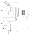
1 shows a wafer cleaning apparatus according to one embodiment.
2 is a view showing a wafer cleaning apparatus according to another embodiment.
3 is a graph showing experimental results of the wafer cleaning apparatus according to the embodiment.
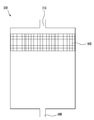
4 is a schematic side cross-sectional view of a first filter according to one embodiment.
5 is a schematic front cross-sectional view of a first filter according to one embodiment.
6 is a schematic view for explaining a general wafer lengthwise apparatus.
Hereinafter, embodiments will be described in detail with reference to the accompanying drawings. The embodiments are to be considered in all aspects as illustrative and not restrictive, and the invention is not limited thereto. It is to be understood, however, that the embodiments are not intended to be limited to the particular forms disclosed, but are to include all modifications, equivalents, and alternatives falling within the spirit and scope of the embodiments. The sizes and shapes of the components shown in the drawings may be exaggerated for clarity and convenience.
The terms "first "," second ", and the like can be used to describe various components, but the components should not be limited by the terms. The terms are used only for the purpose of distinguishing one component from another. In addition, terms specifically defined in consideration of the constitution and operation of the embodiment are only intended to illustrate the embodiments and do not limit the scope of the embodiments.
In the description of the embodiments, when it is described as being formed on the "upper" or "on or under" of each element, the upper or lower (on or under Quot; includes both that the two elements are in direct contact with each other or that one or more other elements are indirectly formed between the two elements. Also, when expressed as "on" or "on or under", it may include not only an upward direction but also a downward direction with respect to one element.
It is also to be understood that the terms "top / top / top" and "bottom / bottom / bottom", as used below, do not necessarily imply nor imply any physical or logical relationship or order between such entities or elements, But may be used only to distinguish one entity or element from another entity or element.
1 is a view showing a wafer W cleaning apparatus according to an embodiment. 1, the wafer W cleaning apparatus of the embodiment includes a
Further, although not shown, a solution replenishing line for replenishing the chemical solution circulated in the wafer W cleaning apparatus may be provided so as to be connected to the
The
The wafer W disposed in the
The wafer W may be polished on both sides through a polishing process. Impurities such as particles generated in the polishing process and foreign substances contained in a slurry used as an abrasive can be adhered to the surface of the wafer W. [ The impurities such as the particles and the foreign substances adhering to the wafer W can be removed by the chemical solution.
The chemical solution flowing into the first filter (100) from the first washing bath (210) may contain the impurities removed from the wafer (W).
Therefore, in order to repeatedly clean the wafer W placed in the
Therefore, the impurities contained in the chemical solution circulating through the
The
The wafer W may be disposed in the
That is, in the
The chemical solution may be temporarily stored in the
The
At this time, impurities removed from the wafer W may be contained in the chemical solution flowing out to the outside through the
1, the
The
The
The
Referring again to FIG. 6, the
The
The
Accordingly, the fine bubbles vented through the
The fine bubbles present in the
Alternatively, the fine bubbles may occur at various locations in the wafer W scrubber. Therefore, in order to prevent the fine bubbles from generating a pattern on the wafer W by etching the wafer W, the fine bubbles are transferred to the wafer W via the
The
Therefore, the fine bubbles mainly present on the upper portion of the
Due to such a structure, at least a part of the fine bubbles existing in the
In addition, since the frequency of occurrence of the pattern due to fine bubbles in the wafer W is reduced, the defect occurrence rate of the wafer W due to pattern generation can be reduced.
Meanwhile, a part of the chemical solution not containing the fine bubbles may be partially introduced into the
The
Due to such a structure, the plurality of
Sectional area and the number of disposing positions of the
The
Therefore, the
The
The chemical solution filtered from the
As shown in FIG. 1, the
Since the density of the fine bubbles is smaller than that of the chemical solution containing no fine bubbles, the fine bubbles may exist mainly on the upper portion of the
Therefore, when the first line is connected to the lower portion of the
The
The
Meanwhile, the
The damper D may be installed in the
This is because when the pump P pumps the chemical solution, the pump P may not constantly pump the chemical solution, and thus the flow rate and flow rate of the chemical solution passing through the pump P It can change irregularly.
Therefore, in order to stabilize the irregular flow of the chemical solution, the damper D may suitably be provided behind the pump P. In another embodiment, the pump P and the damper D may be integrally provided in the
The drain in-
A valve V may be installed in the
Of course, when the liquid inside the filter is drained, the valve (V) can be opened to perform drain operation.
2 is a view showing a wafer W cleaning apparatus according to another embodiment. In the embodiment, the second filter 100-1 is provided to filter the chemical solution containing the impurities together with the
The second filter 100-1, the second vent line 300-1, and the second connection line 400-1 may further include the second filter 100-1, the second vent line 300-1, and the second connection line 400-1. The
The second filter 100-1 may be connected to the
Therefore, the fine bubbles and the chemical solution discharged into the
The second vent line 300-1 may be installed on the
The second connection line 400-1 may connect the second filter 100-1 and the
Similar to the
The wafer W cleaning apparatus using the dual vent system shown in FIG. 2 uses two filters and two vent lines in comparison with the wafer W cleaning apparatus of the embodiment shown in FIG.
Therefore, the wafer W cleaning apparatus of FIG. 2 can more effectively suppress the inflow of fine bubbles into the
In another embodiment, the filter and the vent line may be provided with a wafer W cleaning apparatus having three or more, respectively. The number of filters and vent lines can be appropriately selected in consideration of the overall structure of the wafer (W) cleaning apparatus, manufacturing cost, and the like.
3 is a graph showing experimental results of the wafer W cleaning apparatus according to the embodiment. A cleaning experiment was conducted on a total of 225 pieces of wafers W in the test of the wafer W cleaning apparatus.
In the graph, the vertical axis represents the percentage (%) of the patterns of the 225 wafers W used in the experiment, which are etched by the fine bubbles.
The alphabetic characters on the horizontal axis in the graph are as follows. And X represents a case where the cleaning experiment is carried out in a general wafer (W) cleaning apparatus not provided with the filter and the vent line of the embodiment. At this time, in the case of X, the repeated experiment was performed 9 times in total, and the average value of the pattern occurrence rate due to the fine bubbles of the wafer W was obtained.
Y shows a case where the cleaning experiment is performed in the wafer W cleaning apparatus of the embodiment having the
Z shows the wafer W in the embodiment having the
As a result of the experiment, as shown in FIG. 3, in the case of X, the pattern generation rate is about 15%. However, in the case of Y, the pattern generation ratio is about 10%, which is lower than that of X.
On the other hand, in the case of Z, the pattern occurrence ratio is close to 0%. That is, in the case of Z, it can be seen that a pattern due to fine bubbles is hardly generated in the wafer W.
From the above experimental results, it can be seen that the rate of pattern generation due to fine bubbles is reduced in a wafer W cleaning apparatus having a filter and a vent line, rather than a general wafer W cleaning apparatus.
Further, when a plurality of filters and a plurality of vent lines are used in comparison with the wafer W cleaning apparatus using one filter and one vent line, the pattern generation ratio due to the fine bubbles is remarkably reduced.
In addition, it can be seen that the vent line of the embodiment can very effectively block the inflow of fine bubbles present in the filter into the
4 is a schematic side cross-sectional view of a
Also, the
As shown in FIGS. 4 and 5, the
The
The
Due to such a structure, the fine bubbles flowing into the
Therefore, the collection net 800 blocks the fine bubbles flowing into the
While only a few have been described above with respect to the embodiments, various other forms of implementation are possible. The technical contents of the embodiments described above may be combined in various forms other than the mutually incompatible technologies, and may be implemented in a new embodiment through the same.
11: Wafer guide
100: first filter
100-1: second filter
200: Baths
210: The first taxation
220: Second-tier construction
300: First vent line
300-1: Second vent line
310: Branch engine
320: Head
400: first connection line
400-1: second connection line
500: circulation line
600: drain inline
800: Collection network
P: Pump
D: Damper
V: Valve
W: Wafer
Claims (13)
A bath on which the wafer is placed and to which the chemical solution having passed through the first filter is supplied;
A first vent line disposed above the first filter and venting at least a portion of micro bubbles present in the first filter;
A first connection line connecting the first filter and the bass, and flowing the chemical solution from the first filter to the bass;
Connecting the bath and the first filter, circulating the chemical solution from the bath to the first filter,
And a wafer cleaning apparatus.
Wherein the bath comprises a first cleaning bath in which the wafer is placed and a second cleaning bath in which the chemical solution overflows from the first cleaning bath,
Wherein the first vent line is connected to the second cleaning bath.
The circulation line may include:
And one side is connected to the second cleaning tank.
Wherein the first connection line includes:
And one side is connected to a lower portion of the first filter.
The circulation line may include:
A pump for pumping the chemical solution, and a damper for stabilizing the flow of the chemical solution.
The first vent line
A branch pipe connected to the upper side of the first filter and provided in plurality; And
And a head to which the branch pipes are joined.
And a second filter connected to the circulation line.
A second vent line disposed above the first filter; And
A second connection line connecting the second filter and the bath,
The wafer cleaning apparatus further comprising:
Wherein the circulation line is branched and connected to the first filter and the second filter, respectively.
Wherein,
Wherein the wafer cleaning device is mounted on a wafer guide provided on the bath and is cleaned by the chemical solution.
A bath on which the wafer is placed and to which the chemical solution having passed through the first filter is supplied;
A first vent line disposed above the first filter and venting at least a portion of micro bubbles present in the first filter;
A first connection line connecting the first filter and the bass, and flowing the chemical solution from the first filter to the bass;
A circulation line connecting the bath and the first filter, from which the chemical solution flows from the bath to the first filter;
A second filter connected to the circulation line;
A second vent line disposed above the second filter and venting at least a portion of the fine bubbles present in the second filter; And
A second connection line connecting the second filter and the bath, and a second connection line through which the chemical solution flows from the second filter to the bath,
And a wafer cleaning apparatus.
Wherein the first filter and the second filter include:
Wherein a drain in-line is provided at a lower portion thereof, and a valve is provided at the drain in-line.
The first filter and / or the second filter may comprise:
Further comprising a collecting net disposed at an inner side of the bottom wall and inclined along the width direction to collect the micro bubbles.
Priority Applications (1)
| Application Number | Priority Date | Filing Date | Title |
|---|---|---|---|
| KR1020150186264A KR20170076237A (en) | 2015-12-24 | 2015-12-24 | Wafer cleaning apparatus |
Applications Claiming Priority (1)
| Application Number | Priority Date | Filing Date | Title |
|---|---|---|---|
| KR1020150186264A KR20170076237A (en) | 2015-12-24 | 2015-12-24 | Wafer cleaning apparatus |
Publications (1)
| Publication Number | Publication Date |
|---|---|
| KR20170076237A true KR20170076237A (en) | 2017-07-04 |
Family
ID=59357298
Family Applications (1)
| Application Number | Title | Priority Date | Filing Date |
|---|---|---|---|
| KR1020150186264A KR20170076237A (en) | 2015-12-24 | 2015-12-24 | Wafer cleaning apparatus |
Country Status (1)
| Country | Link |
|---|---|
| KR (1) | KR20170076237A (en) |
-
2015
- 2015-12-24 KR KR1020150186264A patent/KR20170076237A/en not_active Application Discontinuation
Similar Documents
| Publication | Publication Date | Title |
|---|---|---|
| KR20170076237A (en) | Wafer cleaning apparatus | |
| JP2011529395A (en) | Workpiece cleaning device | |
| JP5116628B2 (en) | Cleaning method | |
| JP2006013015A (en) | Cleaning device and cleaning method | |
| JP2008306104A (en) | Device and method of wet treatment | |
| JP2835546B2 (en) | Processing tank for etching etc. | |
| KR101915358B1 (en) | Semiconductor cleaning device and cleaning method by it | |
| KR101000404B1 (en) | Apparatus and method for cleaning wafer | |
| CN210187878U (en) | Storage device for polished wafers | |
| JP3898257B2 (en) | Wafer cleaning apparatus and wafer cleaning method | |
| KR100598914B1 (en) | System and method for recycling chemical, and apparatus for treating a substrate using the system | |
| JP4381944B2 (en) | Particle removal method and substrate processing apparatus | |
| CN109509696B (en) | Water channel device for pre-cleaning machine, pre-cleaning machine and pre-cleaning method | |
| JPH0731810A (en) | Purification of filter in washing process | |
| KR20050003896A (en) | Cleaning solution circulation apparatus in semiconductor manufacturing equipment | |
| KR101392820B1 (en) | Drying apparatus using deionized hot water | |
| JP3099907B2 (en) | Semiconductor processing equipment | |
| KR20030037899A (en) | A bath for semiconductor fabrication | |
| JP2018022714A (en) | Cleaning method of wafer | |
| KR100871824B1 (en) | Treating liquid supply unit and apparatus for treating substrate with the same | |
| JP4487626B2 (en) | Substrate processing apparatus and substrate processing method using the same | |
| KR20060030689A (en) | Substrate cleaning apparatus | |
| JP2007105626A (en) | Substrate treatment apparatus | |
| KR200177330Y1 (en) | Apparatus for cleansing semiconductor wafer | |
| CN115532721A (en) | Method for cleaning surface and air holes of silicon part |
Legal Events
| Date | Code | Title | Description |
|---|---|---|---|
| A201 | Request for examination | ||
| E902 | Notification of reason for refusal | ||
| E601 | Decision to refuse application |