KR20160114627A - Abrasive material having a structured surface - Google Patents
Abrasive material having a structured surface Download PDFInfo
- Publication number
- KR20160114627A KR20160114627A KR1020167022667A KR20167022667A KR20160114627A KR 20160114627 A KR20160114627 A KR 20160114627A KR 1020167022667 A KR1020167022667 A KR 1020167022667A KR 20167022667 A KR20167022667 A KR 20167022667A KR 20160114627 A KR20160114627 A KR 20160114627A
- Authority
- KR
- South Korea
- Prior art keywords
- less
- abrasive
- treatment
- structured surface
- layer
- Prior art date
Links
Images


Classifications
-
- B—PERFORMING OPERATIONS; TRANSPORTING
- B24—GRINDING; POLISHING
- B24B—MACHINES, DEVICES, OR PROCESSES FOR GRINDING OR POLISHING; DRESSING OR CONDITIONING OF ABRADING SURFACES; FEEDING OF GRINDING, POLISHING, OR LAPPING AGENTS
- B24B37/00—Lapping machines or devices; Accessories
- B24B37/11—Lapping tools
- B24B37/20—Lapping pads for working plane surfaces
- B24B37/26—Lapping pads for working plane surfaces characterised by the shape of the lapping pad surface, e.g. grooved
-
- B—PERFORMING OPERATIONS; TRANSPORTING
- B24—GRINDING; POLISHING
- B24B—MACHINES, DEVICES, OR PROCESSES FOR GRINDING OR POLISHING; DRESSING OR CONDITIONING OF ABRADING SURFACES; FEEDING OF GRINDING, POLISHING, OR LAPPING AGENTS
- B24B1/00—Processes of grinding or polishing; Use of auxiliary equipment in connection with such processes
-
- C—CHEMISTRY; METALLURGY
- C23—COATING METALLIC MATERIAL; COATING MATERIAL WITH METALLIC MATERIAL; CHEMICAL SURFACE TREATMENT; DIFFUSION TREATMENT OF METALLIC MATERIAL; COATING BY VACUUM EVAPORATION, BY SPUTTERING, BY ION IMPLANTATION OR BY CHEMICAL VAPOUR DEPOSITION, IN GENERAL; INHIBITING CORROSION OF METALLIC MATERIAL OR INCRUSTATION IN GENERAL
- C23C—COATING METALLIC MATERIAL; COATING MATERIAL WITH METALLIC MATERIAL; SURFACE TREATMENT OF METALLIC MATERIAL BY DIFFUSION INTO THE SURFACE, BY CHEMICAL CONVERSION OR SUBSTITUTION; COATING BY VACUUM EVAPORATION, BY SPUTTERING, BY ION IMPLANTATION OR BY CHEMICAL VAPOUR DEPOSITION, IN GENERAL
- C23C14/00—Coating by vacuum evaporation, by sputtering or by ion implantation of the coating forming material
- C23C14/06—Coating by vacuum evaporation, by sputtering or by ion implantation of the coating forming material characterised by the coating material
- C23C14/0605—Carbon
-
- C—CHEMISTRY; METALLURGY
- C23—COATING METALLIC MATERIAL; COATING MATERIAL WITH METALLIC MATERIAL; CHEMICAL SURFACE TREATMENT; DIFFUSION TREATMENT OF METALLIC MATERIAL; COATING BY VACUUM EVAPORATION, BY SPUTTERING, BY ION IMPLANTATION OR BY CHEMICAL VAPOUR DEPOSITION, IN GENERAL; INHIBITING CORROSION OF METALLIC MATERIAL OR INCRUSTATION IN GENERAL
- C23C—COATING METALLIC MATERIAL; COATING MATERIAL WITH METALLIC MATERIAL; SURFACE TREATMENT OF METALLIC MATERIAL BY DIFFUSION INTO THE SURFACE, BY CHEMICAL CONVERSION OR SUBSTITUTION; COATING BY VACUUM EVAPORATION, BY SPUTTERING, BY ION IMPLANTATION OR BY CHEMICAL VAPOUR DEPOSITION, IN GENERAL
- C23C14/00—Coating by vacuum evaporation, by sputtering or by ion implantation of the coating forming material
- C23C14/06—Coating by vacuum evaporation, by sputtering or by ion implantation of the coating forming material characterised by the coating material
- C23C14/0635—Carbides
-
- C—CHEMISTRY; METALLURGY
- C23—COATING METALLIC MATERIAL; COATING MATERIAL WITH METALLIC MATERIAL; CHEMICAL SURFACE TREATMENT; DIFFUSION TREATMENT OF METALLIC MATERIAL; COATING BY VACUUM EVAPORATION, BY SPUTTERING, BY ION IMPLANTATION OR BY CHEMICAL VAPOUR DEPOSITION, IN GENERAL; INHIBITING CORROSION OF METALLIC MATERIAL OR INCRUSTATION IN GENERAL
- C23C—COATING METALLIC MATERIAL; COATING MATERIAL WITH METALLIC MATERIAL; SURFACE TREATMENT OF METALLIC MATERIAL BY DIFFUSION INTO THE SURFACE, BY CHEMICAL CONVERSION OR SUBSTITUTION; COATING BY VACUUM EVAPORATION, BY SPUTTERING, BY ION IMPLANTATION OR BY CHEMICAL VAPOUR DEPOSITION, IN GENERAL
- C23C16/00—Chemical coating by decomposition of gaseous compounds, without leaving reaction products of surface material in the coating, i.e. chemical vapour deposition [CVD] processes
- C23C16/22—Chemical coating by decomposition of gaseous compounds, without leaving reaction products of surface material in the coating, i.e. chemical vapour deposition [CVD] processes characterised by the deposition of inorganic material, other than metallic material
- C23C16/26—Deposition of carbon only
-
- C—CHEMISTRY; METALLURGY
- C23—COATING METALLIC MATERIAL; COATING MATERIAL WITH METALLIC MATERIAL; CHEMICAL SURFACE TREATMENT; DIFFUSION TREATMENT OF METALLIC MATERIAL; COATING BY VACUUM EVAPORATION, BY SPUTTERING, BY ION IMPLANTATION OR BY CHEMICAL VAPOUR DEPOSITION, IN GENERAL; INHIBITING CORROSION OF METALLIC MATERIAL OR INCRUSTATION IN GENERAL
- C23C—COATING METALLIC MATERIAL; COATING MATERIAL WITH METALLIC MATERIAL; SURFACE TREATMENT OF METALLIC MATERIAL BY DIFFUSION INTO THE SURFACE, BY CHEMICAL CONVERSION OR SUBSTITUTION; COATING BY VACUUM EVAPORATION, BY SPUTTERING, BY ION IMPLANTATION OR BY CHEMICAL VAPOUR DEPOSITION, IN GENERAL
- C23C16/00—Chemical coating by decomposition of gaseous compounds, without leaving reaction products of surface material in the coating, i.e. chemical vapour deposition [CVD] processes
- C23C16/22—Chemical coating by decomposition of gaseous compounds, without leaving reaction products of surface material in the coating, i.e. chemical vapour deposition [CVD] processes characterised by the deposition of inorganic material, other than metallic material
- C23C16/30—Deposition of compounds, mixtures or solid solutions, e.g. borides, carbides, nitrides
- C23C16/32—Carbides
- C23C16/325—Silicon carbide
-
- C—CHEMISTRY; METALLURGY
- C23—COATING METALLIC MATERIAL; COATING MATERIAL WITH METALLIC MATERIAL; CHEMICAL SURFACE TREATMENT; DIFFUSION TREATMENT OF METALLIC MATERIAL; COATING BY VACUUM EVAPORATION, BY SPUTTERING, BY ION IMPLANTATION OR BY CHEMICAL VAPOUR DEPOSITION, IN GENERAL; INHIBITING CORROSION OF METALLIC MATERIAL OR INCRUSTATION IN GENERAL
- C23C—COATING METALLIC MATERIAL; COATING MATERIAL WITH METALLIC MATERIAL; SURFACE TREATMENT OF METALLIC MATERIAL BY DIFFUSION INTO THE SURFACE, BY CHEMICAL CONVERSION OR SUBSTITUTION; COATING BY VACUUM EVAPORATION, BY SPUTTERING, BY ION IMPLANTATION OR BY CHEMICAL VAPOUR DEPOSITION, IN GENERAL
- C23C16/00—Chemical coating by decomposition of gaseous compounds, without leaving reaction products of surface material in the coating, i.e. chemical vapour deposition [CVD] processes
- C23C16/44—Chemical coating by decomposition of gaseous compounds, without leaving reaction products of surface material in the coating, i.e. chemical vapour deposition [CVD] processes characterised by the method of coating
- C23C16/455—Chemical coating by decomposition of gaseous compounds, without leaving reaction products of surface material in the coating, i.e. chemical vapour deposition [CVD] processes characterised by the method of coating characterised by the method used for introducing gases into reaction chamber or for modifying gas flows in reaction chamber
- C23C16/45523—Pulsed gas flow or change of composition over time
- C23C16/45525—Atomic layer deposition [ALD]
Abstract
이물질의 접착 및 축적을 방지하는 데 뛰어난 구조화된 표면을 갖는 연마 재료, 및 이의 제조 방법을 제공함.
본 발명의 실시 형태의 연마 재료는 상부에 배열된 복수의 3차원 요소를 갖는 구조화된 표면을 가진 연마 층을 갖는 연마 재료로서, 불소 처리 및 규소 처리로 이루어진 군으로부터 선택되는 표면 처리가 구조화된 표면의 적어도 일부에 대해 수행되며, 불소 처리는 플라즈마 처리, 화학 증착, 물리 증착, 및 불소 기체 처리로 이루어진 군으로부터 선택되는, 연마 재료이다.A polishing material having an excellent structured surface for preventing adhesion and accumulation of foreign matter, and a method for manufacturing the same.
An abrasive material of an embodiment of the present invention is an abrasive material having an abrasive layer having a structured surface having a plurality of three-dimensional elements arranged thereon, wherein a surface treatment selected from the group consisting of fluorine treatment and silicon treatment is applied to the structured surface Wherein the fluorine treatment is selected from the group consisting of plasma treatment, chemical vapor deposition, physical vapor deposition, and fluorine gas treatment.
Description
본 발명은 구조화된 표면(structured surface)을 갖는 연마 재료에 관한 것이다. 특히, 본 발명은 표면 처리된 구조화된 표면을 갖는 연마 층을 포함하는 연마 재료에 관한 것이다.The present invention relates to an abrasive material having a structured surface. In particular, the present invention relates to a polishing material comprising an abrasive layer having a surface-treated structured surface.
연마 재료는 반도체 웨이퍼, 자기 기록 매체, 유리 판, 렌즈, 프리즘, 자동차 도장된 표면, 광섬유 커넥터 단부 표면 등과 같은 다양한 표면의 거친 폴리싱(rough polishing), 챔퍼링(chamfering), 마무리 폴리싱(final polishing) 등에서 널리 사용된다.The abrasive material may be used for rough polishing, chamfering, final polishing of various surfaces such as semiconductor wafers, magnetic recording media, glass plates, lenses, prisms, automotive painted surfaces, fiber optic connector end surfaces, And so on.
예를 들어, 반도체 웨이퍼의 화학 기계적 폴리싱(chemical mechanical polishing, CMP) 공정에서, 사각뿔 형상, 반구 형상 등을 갖는 3차원 요소와 같은 복수의 3차원 요소를 체계적으로 배치한 구조화된 표면을 갖는 연마 층을 포함하는 연마 재료 (컨디셔너(conditioner) 또는 드레서 디스크(dresser disk)로 또한 지칭됨)가 폴리싱 패드의 거친 폴리싱 (드레싱 또는 컨디셔닝으로 또한 지칭됨)을 위해 사용된다. CMP 공정은 폴리싱 패드와 반도체 웨이퍼 사이에 연마 입자를 포함하는 슬러리(slurry)를 제공함으로써 CMP를 수행하는 단계를 포함한다. 컨디셔너는 연마 층으로서 모놀리식(monolithic) 다이아몬드 층으로 코팅된 탄화규소 층을 포함하고, 예를 들어 지지 디스크 또는 링에 부착된다. 연마 재료는 폴리싱 패드의 표면을 조면화하고, 폴리싱 패드 표면의 막힘(clogging)을 제거한다. CMP 공정은 이러한 방식으로 안정화된다. 구조화된 표면을 갖는 연마 층을 포함하는 이러한 종류의 컨디셔너는, 니켈 도금, 납땜, 소결 등에 의해 베이스 재료(base material) 상에 접착된 응집 다이아몬드 입자와 같은 연마 입자를 갖는 다른 종래의 컨디셔너에 비해, 탈락된(dislodged) 연마 입자에 의해 유발되는 대형 스크래치가 반도체 웨이퍼 표면 상에서 발생하지 않는다는 점에서 유리하다.For example, in a chemical mechanical polishing (CMP) process of a semiconductor wafer, an abrasive layer having a structured surface in which a plurality of three-dimensional elements such as a three-dimensional element having a quadrangular pyramid shape, (Also referred to as a conditioner or a dresser disk) is used for rough polishing (also referred to as dressing or conditioning) of the polishing pad. The CMP process includes performing CMP by providing a slurry containing abrasive particles between the polishing pad and the semiconductor wafer. The conditioner comprises a layer of silicon carbide coated with a monolithic diamond layer as an abrasive layer, for example, attached to a support disk or ring. The polishing material roughenes the surface of the polishing pad and removes clogging of the polishing pad surface. The CMP process is stabilized in this way. This type of conditioner comprising an abrasive layer having a structured surface is superior to other conventional conditioners having abrasive particles such as cohesive diamond particles adhered on a base material by nickel plating, brazing, sintering, It is advantageous in that large scratches caused by dislodged abrasive particles do not occur on the semiconductor wafer surface.
구조화된 표면을 갖는 연마 재료는 또한 액정 디스플레이 제조 등에서 사용되는 대형 유리 판의 표면 폴리싱에서, 광섬유 커넥터 단부 표면, 자동차 도장된 표면 등의 거친 폴리싱 및 마무리 폴리싱에서 사용된다. 예를 들어, 연마 층이 응집 다이아몬드 입자, 알루미나, 탄화규소, 산화세륨 등과 같은 연마 입자, 및 경화된 우레탄 아크릴레이트, 에폭시 수지 등과 같은 결합제를 포함하는 연마 재료가 사용된다. 폴리싱될 물체와 접촉하는 연마 층의 부분은 폴리싱될 물체의 경도에 따라 거친 폴리싱 또는 마무리 폴리싱 동안에 마모되고, 새로운 연마 입자가 구조화된 표면 상에서 노출된다. 예를 들어, 유리 판 등의 경도를 갖는 폴리싱될 물체가 폴리싱되는 경우, 연마 층은 보통 폴리싱 동안 마모된다. 반면에, 최외측 층에서 아크릴 수지, 우레탄 수지 등을 사용하는 자동차 도장된 표면과 같은 저 경도를 갖는 표면이 폴리싱되는 경우, 연마 층은 유의하게 마모되지 않을 수 있다.Abrasive materials having structured surfaces are also used in the surface polishing of large glass plates used in the manufacture of liquid crystal displays and the like, in rough polishing and finishing polishing of optical fiber connector end surfaces, automotive painted surfaces and the like. For example, an abrasive material is used in which the abrasive layer comprises abrasive grains such as agglomerated diamond particles, alumina, silicon carbide, cerium oxide, and the like, and a binder such as hardened urethane acrylate, epoxy resin and the like. The portion of the abrasive layer that is in contact with the object to be polished is abraded during coarse polishing or finish polishing depending on the hardness of the object to be polished and new abrasive particles are exposed on the structured surface. For example, when an object to be polished having a hardness such as a glass plate is polished, the polishing layer is usually worn during polishing. On the other hand, when a surface having a low hardness such as an automotive painted surface using an acrylic resin, a urethane resin or the like is polished in the outermost layer, the abrasive layer may not be significantly worn.
특허문헌 1 (국제 공개 WO 2005-012592호)은 (a) (1) 적어도 하나의 유형의 세라믹 재료를 함유하는 제1 상(phase), 및 (2) 적어도 하나의 유형의 탄화물 형성 재료를 포함하는 제2 상을 포함하는 표면을 갖는 베이스 재료; 및 (b) 베이스 재료의 표면의 적어도 일부 상에 배치된 화학 증착 다이아몬드 코팅을 포함하는 CVD 다이아몬드 코팅 복합 재료를 기술하고 있다.Patent Document 1 (International Publication No. WO 2005-012592) discloses a method of manufacturing a ceramic material which comprises (a) (1) a first phase containing at least one type of ceramic material, and (2) at least one type of carbide- A base material having a surface comprising a second phase; And (b) a CVD diamond coating disposed on at least a portion of the surface of the base material.
특허문헌 2 (공개된 PCT 출원 제2002-542057호의 일본어 번역문)는 "배킹 재료(backing material) 및 배킹 재료의 표면 상에 결합된 적어도 하나의 3차원 연마 코팅을 포함하며, 연마 코팅은 복수의 다이아몬드 비드 연마 입자를 분산시킨 경화된 결합제 전구체로부터 형성된 결합제 및 연마 코팅의 대략 40 내지 대략 60 중량%를 구성하는 충전제를 포함하는, 유리 또는 유리 세라믹 작업물(work piece)을 폴리싱하는 데 이상적인 연마 물품"을 기술하고 있다.Patent Document 2 (published in Japanese translation of PCT Application No. 2002-542057) discloses "a backing material and at least one three-dimensional abrasive coating bonded on the surface of the backing material, the abrasive coating comprising a plurality of diamonds An abrasive article that is ideal for polishing a glass or glass ceramic work piece comprising a binder formed from a cured binder precursor in which bead abrasive particles are dispersed and a filler that constitutes about 40 to about 60 weight percent of the abrasive coating, .
특허문헌 3 (일본 특허 출원 공개 제2001-179640호)은 "광섬유 커넥터 단부 표면을 미리 결정된 형상으로 폴리싱하는 데 사용되는 연마 재료로서, 연마 재료는 베이스 재료 및 베이스 재료 상에 제공된 연마 층을 포함하며, 연마 층은 구성요소로서 연마 입자 및 결합제를 포함하는 연마 복합재를 갖고, 연마 층은 미리 결정된 형상의 복수의 체계적으로 배치된 입체 요소에 의해 구성된 공간적 구조를 갖는, 연마 재료"를 기술한다.Patent Document 3 (Japanese Patent Application Laid-Open No. 2001-179640) discloses an abrasive material used for polishing an optical fiber connector end surface in a predetermined shape, the abrasive material including a base material and an abrasive layer provided on the base material , The abrasive layer having abrasive composites comprising abrasive particles and a binder as constituent elements and the abrasive layer having a spatial structure constituted by a plurality of systematically arranged three-dimensional elements of a predetermined shape ".
특허문헌 1: 국제 공개 WO 2005/012592호Patent Document 1: International Publication No. WO 2005/012592
특허문헌 2: 공개된 PCT 출원 제2002-542057호의 일본어 번역문Patent Document 2: Japanese translation of Published PCT Application No. 2002-542057
특허문헌 3: 일본 특허 출원 공개 제2001-179640호Patent Document 3: Japanese Patent Application Laid-Open No. 2001-179640
원인은 불명확하지만, 구조화된 표면을 갖는 연마 층을 포함하는 연마 재료를 사용하는 CMP 공정 동안 우레탄 폼 패드 컨디셔닝이 수행될 때, 반도체 웨이퍼 표면의 결함 밀도가 컨디셔닝 주기의 증가와 함께 증가할 수 있다. 더욱이, CMP 슬러리에 포함된 연마 입자, 우레탄 폼 패드로부터 떨어진 폴리우레탄 입자 등과 같은 이물질(foreign object)의 축적이 연마 층의 구조화된 표면의 밸리 부분(valley part) (오목 부분)에서 관찰될 수 있다. 이물질의 축적은 연마 재료와 우레탄 폼 패드 사이에서의 CMP 슬러리의 매끄러운 유동을 방해하는 것으로 여겨진다.The cause is unclear, but when the urethane foam pad conditioning is performed during a CMP process using an abrasive material comprising an abrasive layer having a structured surface, the defect density of the semiconductor wafer surface may increase with increasing the conditioning period. Moreover, the accumulation of foreign objects such as abrasive particles contained in the CMP slurry, polyurethane particles away from the urethane foam pad, etc. can be observed in the valley part (concave portion) of the structured surface of the abrasive layer . Accumulation of foreign matter is believed to interfere with the smooth flow of the CMP slurry between the abrasive material and the urethane foam pad.
구조화된 표면의 밸리 부분에서의 유리 판의 표면 폴리싱에 의해 떨어진 유리 분말 (폴리싱 분말)의 축적, 및 자동차 도장된 표면을 거친 폴리싱 및 마무리 폴리싱할 때 아크릴 수지, 우레탄 수지 등과 같은 구조화된 표면에의 접착 (이 경우, 연마 층은 유의하게 마모되지 않고, 접착은 구조화된 표면의 돌출 부분 또는 팁(tip)에서 발생함)은 바람직하게는 방지되거나 억제되는데, 왜냐하면 생산 효율이 감소될 수 있고, 이에 따라 제품 품질에 영향을 미칠 수 있기 때문이다.The accumulation of glass powder (polishing powder) dropped by the surface polishing of the glass plate in the valley portion of the structured surface, and the accumulation of glass powder (polishing powder) on the structured surface such as acrylic resin, urethane resin and the like The adhesion (in this case, the abrasive layer is not significantly worn, adhesion occurs at the protruding portion or tip of the structured surface) is preferably prevented or inhibited because the production efficiency can be reduced, This can affect product quality.
본 발명의 목적은 이물질의 접착 및 축적을 방지하는 데 뛰어난 구조화된 표면을 갖는 연마 재료, 및 이의 제조 방법을 제공하는 것이다.An object of the present invention is to provide an abrasive material having an excellent structured surface for preventing adhesion and accumulation of foreign matter, and a method of manufacturing the same.
본 발명의 실시 형태는 상부에 배열된 복수의 3차원 요소를 갖는 구조화된 표면을 가진 연마 층을 갖는 연마 재료로서, 불소 처리 및 규소 처리로 이루어진 군으로부터 선택되는 표면 처리가 구조화된 표면의 적어도 일부에 대해 수행되며, 불소 처리는 플라즈마 처리, 화학 증착, 물리 증착, 및 불소 기체 처리로 이루어진 군으로부터 선택되는, 연마 재료를 제공한다.An embodiment of the present invention is an abrasive material having an abrasive layer having a structured surface having a plurality of three-dimensional elements arranged thereon, the abrasive material having a surface treatment selected from the group consisting of fluorine treatment and silicon treatment, Wherein the fluorine treatment is selected from the group consisting of plasma treatment, chemical vapor deposition, physical vapor deposition, and fluorine gas treatment.
본 발명의 다른 실시 형태는 상부에 배열된 복수의 3차원 요소를 갖는 구조화된 표면을 가진 연마 층을 포함하는 연마 재료를 제공하는 단계; 및 불소 처리 및 규소 처리로 이루어진 군으로부터 선택되는 표면 처리를 연마 재료의 구조화된 표면의 적어도 일부에 대해 수행하는 단계를 포함하며, 불소 처리는 플라즈마 처리, 화학 증착, 물리 증착, 및 불소 기체 처리로 이루어진 군으로부터 선택되는, 연마 재료의 제조 방법을 제공한다.Another embodiment of the present invention provides a method of polishing a substrate, comprising: providing an abrasive material comprising an abrasive layer having a structured surface having a plurality of three-dimensional elements arranged thereon; And performing a surface treatment selected from the group consisting of fluorine treatment and silicon treatment on at least a portion of the structured surface of the abrasive material, wherein the fluorine treatment is performed by plasma treatment, chemical vapor deposition, physical vapor deposition, and fluorine gas treatment Wherein the polishing agent is selected from the group consisting of
본 발명의 또 다른 실시 형태는 상부에 배열된 복수의 3차원 요소를 갖도록 구성된 구조화된 표면을 가진 연마 층을 갖는 연마 재료로서, 구조화된 표면의 적어도 일부는, (a) 고밀화 플루오로카본, 옥시탄화규소, 및 산화규소로 이루어진 군으로부터 선택되는 재료를 포함하는 필름; (b) 불소 종결된 표면; 또는 (c) 이들의 조합을 포함하는, 연마 재료를 제공한다.Yet another embodiment of the present invention is an abrasive material having an abrasive layer having a structured surface configured to have a plurality of three-dimensional elements arranged thereon, wherein at least a portion of the structured surface comprises: (a) densified fluorocarbon, A film comprising a material selected from the group consisting of silicon carbide, and silicon oxide; (b) a fluorine terminated surface; Or (c) a combination thereof.
본 발명에 따르면, 구조화된 표면, 특히 구조화된 표면의 밸리 부분 (오목 부분)에서 이물질이 접착되거나 축적됨이 없이 방출될 수 있는 연마 재료가 제공될 수 있다.According to the present invention, it is possible to provide an abrasive material which can be released without any foreign matter adhering or accumulating on the structured surface, especially in the valley portion (concave portion) of the structured surface.
상기의 설명은 본 발명의 모든 실시 형태 또는 본 발명에 관련된 이점의 완전한 개시로서 간주되어서는 안 된다는 것에 유의한다.It should be noted that the above description should not be construed as a complete disclosure of all embodiments of the invention or the advantages associated with the invention.
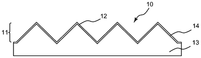
도 1은 본 발명의 실시 형태의 연마 재료의 단면도이다.
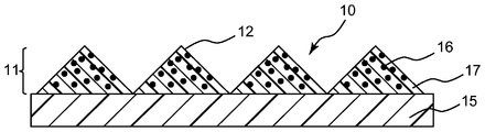
도 2는 본 발명의 다른 실시 형태의 연마 재료의 단면도이다.
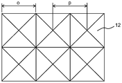
도 3a는 삼각뿔 형상을 갖는 복수의 3차원 요소가 배치된 구조화된 표면의 상부 표면 개략도이다.
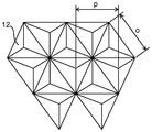
도 3b는 사각뿔 형상을 갖는 복수의 3차원 요소가 배치된 구조화된 표면의 상부 표면 개략도이다.
도 3c는 절두형 각뿔 형상(truncated pyramid shape)을 갖는 복수의 3차원 요소가 배치된 구조화된 표면의 상부 표면 개략도이다.
도 3d는 반구 형상을 갖는 복수의 3차원 요소가 배치된 구조화된 표면의 상부 표면 개략도이다.
도 3e는 3차원 요소가 측방향으로 배향 및 정렬된 삼각형 프리즘인 구조화된 표면의 단면도이다.
도 3f는 모임 지붕 형상(hipped roof shape)을 갖는 복수의 3차원 요소가 배치된 구조화된 표면의 상부 표면 개략도이다.
도 3g는 다양한 형상의 복수의 3차원 요소의 조합이 배치된 구조화된 표면의 상부 표면 개략도이다.
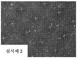
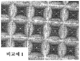
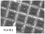
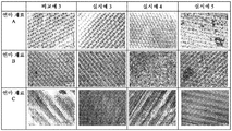
도 4a 내지 도 4d는 CMP 드레싱 시험을 수행한 후의, 각각, 실시예 1 및 실시예 2와 비교예 1 및 비교예 2의 연마 재료의 구조화된 표면의 광학 현미경 사진이다.
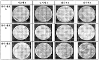
도 5a는 자동차 코팅 폴리싱 시험을 수행한 후의, 실시예 3 내지 실시예 5와 비교예 3의 연마 재료 A 내지 연마 재료 C의 전체 사진이다.
도 5b는 자동차 코팅 폴리싱 시험을 수행한 후의, 실시예 3 내지 실시예 5와 비교예 3의 연마 재료 A 내지 연마 재료 C의 구조화된 표면의 광학 현미경 사진이다.
도 5c는 자동차 코팅 폴리싱 시험을 수행하고 이어서 물로 세정한 후의, 실시예 3 내지 실시예 5와 비교예 3의 연마 재료 A 내지 연마 재료 C의 구조화된 표면의 광학 현미경 사진이다.1 is a cross-sectional view of an abrasive material according to an embodiment of the present invention.
2 is a cross-sectional view of an abrasive material according to another embodiment of the present invention.
3A is a top surface schematic view of a structured surface in which a plurality of three-dimensional elements having a triangular pyramid shape are disposed.
3B is a top surface schematic view of a structured surface in which a plurality of three-dimensional elements having a quadrangular pyramidal shape are disposed.
3C is a top surface schematic view of a structured surface in which a plurality of three-dimensional elements having a truncated pyramid shape are disposed.
FIG. 3D is a top surface schematic view of a structured surface in which a plurality of three-dimensional elements having a hemispherical shape are disposed.
Figure 3e is a cross-sectional view of a structured surface in which the three-dimensional element is a laterally oriented and aligned triangular prism.
Figure 3f is a top surface schematic view of a structured surface having a plurality of three-dimensional elements disposed thereon with a hipped roof shape.
Figure 3g is a top surface schematic view of a structured surface in which a combination of a plurality of three-dimensional elements of various shapes is disposed.
4A to 4D are optical micrographs of structured surfaces of the abrasive materials of Examples 1 and 2 and Comparative Example 1 and Comparative Example 2, respectively, after performing the CMP dressing test.
5A is an overall photograph of polishing materials A to C of Examples 3 to 5 and Comparative Example 3 after car-coating polishing test.
5B is an optical microscope photograph of the structured surfaces of the polishing materials A to C of Examples 3 to 5 and Comparative Example 3 after performing the automotive coating polishing test.
5C is an optical microscope picture of the structured surfaces of polishing materials A to C of Examples 3 to 5 and Comparative Example 3 after car coating polishing test is performed and then with water.
본 발명의 대표적인 실시 형태의 예시를 목적으로 하는 상세한 설명이 하기에 주어지지만, 이들 실시 형태는 본 발명을 제한하는 것으로 해석되어서는 안 된다.DETAILED DESCRIPTION OF THE PREFERRED EMBODIMENTS The following detailed description is given for the purpose of illustrating exemplary embodiments of the present invention, but these embodiments are not to be construed as limiting the present invention.
본 개시에서 "연마 표면"은 폴리싱될 물체와의 접촉 표면, 다시 말하면, 연마 재료가 폴리싱될 평평한 물체와 접촉할 때 폴리싱될 물체의 표면에 평행한 수평면을 지칭한다.Refers to a contact surface with an object to be polished, i. E., A horizontal plane parallel to the surface of the object to be polished when the polishing material is contacted with a flat object to be polished.
본 개시에서 3차원 요소의 "높이"는 연마 표면의 수직 선을 따른, 3차원 요소의 하단부 표면으로부터 3차원 요소의 상단부 지점 또는 상단부 표면까지의 거리를 지칭한다.The term "height" of a three-dimensional element in the present disclosure refers to the distance from the lower end surface of the three-dimensional element along the vertical line of the polishing surface to the upper end point or top surface of the three-dimensional element.
본 발명의 실시 형태의 연마 재료는 구조화된 표면을 갖는 연마 층을 포함하고, 복수의 3차원 요소가 구조화된 표면 상에 배치된다. 불소 처리 또는 규소 처리로 이루어진 군으로부터 선택되는 표면 처리가 구조화된 표면의 적어도 일부에 대해 수행된다. 본 개시에서 "불소 처리"는 불소를 함유하는 재료를 사용하는 표면 처리를 지칭하고, "규소 처리"는 규소를 함유하는 재료를 사용하는 표면 처리를 지칭한다. 불소 및 규소 이외의 다른 원자, 예컨대 수소, 산소, 탄소, 질소 등이 표면 처리에서 기여할 수 있고, 이러한 다른 원자는 불소를 함유하는 재료 또는 규소를 함유하는 재료로부터 유래될 수 있거나, 다른 공급원으로부터 유래될 수 있다.An abrasive material of an embodiment of the present invention comprises an abrasive layer having a structured surface and a plurality of three-dimensional elements are disposed on the structured surface. A surface treatment selected from the group consisting of fluorine treatment or silicon treatment is performed on at least a part of the structured surface. In the present disclosure, "fluorine treatment" refers to surface treatment using a fluorine-containing material, and "silicon treatment" refers to surface treatment using a material containing silicon. Fluorine and other atoms other than silicon, such as hydrogen, oxygen, carbon, nitrogen, etc., can contribute to the surface treatment, and these other atoms can be derived from materials containing fluorine or silicon, .
연마 층은 다양한 재료를 사용하여 형성될 수 있다. 도 1은 본 발명의 실시 형태의 연마 재료의 단면도를 예시한다. 도 1에 예시된 연마 재료(10)는 연마 층(11)을 포함하고, 연마 층(11)은 벌크 층(bulk layer)(13) 및 벌크 층(13)의 적어도 일부 상에 배치된 표면 코팅 층(14)을 포함한다. 표면 코팅 층(14)은 복수의 3차원 요소(12)가 배치된 구조화된 표면에 적용된다. 도 1에 예시된 실시 형태에서, 벌크 층(13)은 3차원 요소(12)의 형상을 결정할 뿐만 아니라, 연마 재료(10)를 다른 도구 등에 부착하기 위한 베이스 재료로서 기능한다. 다른 베이스 재료가 구조화된 표면과는 반대편에 있는 측에서 벌크 층(13)의 표면에 부착될 수 있다.The abrasive layer can be formed using various materials. 1 illustrates a cross-sectional view of an abrasive material of an embodiment of the present invention. The
벌크 층은 3차원 요소의 형상을 결정한다. 벌크 층은, 폴리싱될 물체의 재료 특성 및 경도 등을 고려하여, 예를 들어 소결된 세라믹과 같은 무기 재료와 같은 다양한 경질 재료에 의해 형성될 수 있다. 소결된 세라믹에는, 예를 들어 탄화규소, 질화규소, 알루미나, 지르코니아, 탄화텅스텐 등이 포함될 수 있다. 이들 중에서, 탄화규소 및 질화규소, 그리고 특히 탄화규소가 강도, 경도, 내마모성 등의 관점에서 유리하게 사용될 수 있다.The bulk layer determines the shape of the three-dimensional element. The bulk layer may be formed of various hard materials such as an inorganic material such as sintered ceramics in consideration of the material properties and hardness of the object to be polished. The sintered ceramics may include, for example, silicon carbide, silicon nitride, alumina, zirconia, tungsten carbide, and the like. Of these, silicon carbide and silicon nitride, and particularly silicon carbide, can be advantageously used in terms of strength, hardness, abrasion resistance, and the like.
벌크 층은 탄화규소 등과 같은 세라믹 입자, 결합제, 및 필요에 따라 다른 재료를 혼합하고, 구조화된 표면의 네거티브 패턴(negative pattern)을 갖는 금속 다이(die) 내로 가압 사출하고, 이어서 소결함으로써 형성될 수 있다.The bulk layer may be formed by mixing ceramic particles such as silicon carbide, a binder, and other materials as needed, and extruding them into a metal die having a negative pattern of the structured surface followed by sintering have.
표면 코팅 층은 일반적으로 벌크 층보다 더 경질인 재료에 의해 형성되고, 폴리싱 동안 폴리싱될 물체와 접촉함으로써 폴리싱될 물체를 폴리싱하는 데 기여한다. 사용될 수 있는 표면 코팅 층의 예에는 다이아몬드-유사 탄소(diamond-like carbon) (DLC로 약칭됨), 및 다른 다이아몬드 재료, 탄화텅스텐 (WC), 질화티탄 (TiN), 탄화티탄 (TiC) 등이 포함된다. 표면 코팅 층의 두께는 일반적으로 대략 0.5 μm 이상 또는 대략 1 μm 이상, 및 대략 30 μm 이하 또는 대략 20 μm 이하이다. 표면 코팅 층의 두께를 대략 1 μm 이상으로 설정함으로써, 단지 표면 코팅 층만이 폴리싱 동안 폴리싱될 물체와 접촉하고, 이에 따라 폴리싱될 물체는 벌크 층과의 접촉으로부터 보호될 수 있다. 반면에, 표면 코팅 층과 벌크 층의 접착력이 낮은 경우, 표면 코팅 층의 두께는 바람직하게는 비교적 얇게 만들어진다.The surface coating layer is generally formed of a material that is harder than the bulk layer and contributes to polishing the object to be polished by contacting the object to be polished during polishing. Examples of surface coating layers that can be used include diamond-like carbon (abbreviated as DLC) and other diamond materials, tungsten carbide (WC), titanium nitride (TiN), titanium carbide . The thickness of the surface coating layer is generally greater than about 0.5 占 퐉 or about 1 占 퐉 or more, and about 30 占 퐉 or less or about 20 占 퐉 or less. By setting the thickness of the surface coating layer to approximately 1 占 퐉 or more, only the surface coating layer is contacted with the object to be polished during polishing, so that the object to be polished can be protected from contact with the bulk layer. On the other hand, when the adhesion between the surface coating layer and the bulk layer is low, the thickness of the surface coating layer is preferably made relatively thin.
다이아몬드 재료를 함유한 필름이 표면 코팅 층으로서 유리하게 사용될 수 있다. 필름은 예를 들어 다이아몬드-유사 탄소를 포함할 수 있다. 다이아몬드-유사 탄소는 비정질이고, 수소에 의해 안정화된 다량의 sp3을 포함한다 (예를 들어, 탄소 원자는 대략 40 원자% 이상 또는 대략 50 원자% 이상, 및 대략 99 원자% 이하 또는 대략 98 원자% 이하이다). 다이아몬드 필름은 기체 탄소 공급원, 예컨대 메탄 등 또는 고체 탄소 공급원, 예컨대 흑연 등, 및 필요에 따라 수소를 사용하여, 플라즈마 강화 화학 증착 (PECVD) 방법, 핫 와이어 화학 증착 (HWCVD) 방법, 이온 빔, 레이저 어블레이션, RF 플라즈마, 초음파, 아크 방전, 캐소드 아크 플라즈마 침착 등과 같은 종래의 기술에 의해 벌크 층 상에 침착될 수 있다. 일부 실시 형태에서, 고 결정도를 갖는 필름이 안정화되고 생성될 수 있으며, 이에 따라 HWCVD 방법이 두꺼운 다이아몬드 필름을 침착하는 데 유리하게 사용될 수 있다.A film containing a diamond material can be advantageously used as a surface coating layer. The film may comprise, for example, diamond-like carbon. The diamond-like carbon is amorphous and comprises a large amount of sp 3 stabilized by hydrogen (for example, carbon atoms can be at least about 40 atomic percent, or at least about 50 atomic percent, and about 99 atomic percent or about 98 atoms %). The diamond film can be formed by a plasma enhanced chemical vapor deposition (PECVD) method, a hot wire chemical vapor deposition (HWCVD) method, an ion beam, a laser, or the like, using a gaseous carbon source such as methane or the like or a solid carbon source such as graphite, Can be deposited on the bulk layer by conventional techniques such as sputtering, ablation, RF plasma, ultrasonic, arc discharge, cathode arc plasma deposition, and the like. In some embodiments, a film having a high degree of crystallinity can be stabilized and produced, and thus the HWCVD method can be advantageously used to deposit a thick diamond film.
도 2는 본 발명의 다른 실시 형태의 연마 재료의 단면도를 예시한다. 도 2에 예시된 연마 재료(10)는 배킹 재료(15) 상에 연마 입자(16) 및 결합제(17)를 포함하는 연마 층(11)을 포함하고, 연마 층(11)은 복수의 3차원 요소(12)가 배치된 구조화된 표면을 갖는다. 배킹 재료(15)는 연마 재료(10)의 베이스 재료로서의 역할을 한다. 연마 입자(16)는 결합제(17) 전체를 걸쳐 균일하게 또는 비균일하게 분포된다. 이러한 실시 형태에서, 폴리싱될 물체의 표면이 연마 재료(10)를 사용하여 폴리싱될 때, 폴리싱될 물체와 접촉하는 부분이, 폴리싱될 물체의 경도에 따라, 점차적으로 파괴됨으로써, 미사용된 연마 입자(16)를 노출시킨다.Figure 2 illustrates a cross-sectional view of an abrasive material of another embodiment of the present invention. The
이러한 실시 형태에서, 연마 입자, 결합제 전구체, 및 개시제를 포함하는 경화성 조성물이 구조화된 표면의 네거티브 패턴을 갖는 금속 다이 내로 충전되고, 조성물은 열 또는 방사선을 사용하여 경화되며, 이에 따라 연마 입자 및 결합제를 포함하는 연마 층이 형성될 수 있다.In this embodiment, a curable composition comprising abrasive particles, a binder precursor, and an initiator is filled into a metal die having a negative pattern of the structured surface, and the composition is cured using heat or radiation, May be formed.
사용될 수 있는 연마 입자의 예에는 다이아몬드, 입방정 질화붕소, 산화세륨, 용융 산화알루미늄, 열처리된 산화알루미늄, 졸-겔(sol-gel) 공정에 의해 제조된 산화알루미늄, 탄화규소, 산화크롬, 실리카, 지르코니아, 알루미나 지르코니아, 산화철, 가닛(garnet) 및 이들의 혼합물이 포함된다. 연마 입자의 모스 경도(Mohs' hardness)는 바람직하게는 8 이상 또는 9 이상이다. 연마 입자의 유형은 의도된 폴리싱에 기초해 선택될 수 있고, 다이아몬드, 입방정 질화붕소, 산화알루미늄 및 탄화규소가 디버링(deburring) 등과 같은 거친 폴리싱에, 그리고 만곡된 표면 형성 등과 같은 챔퍼링에 유리하게 사용될 수 있고, 실리카 및 산화알루미늄이 마무리 폴리싱에 유리하게 사용될 수 있다.Examples of abrasive particles that can be used include diamond, cubic boron nitride, cerium oxide, molten aluminum oxide, heat-treated aluminum oxide, aluminum oxide made by a sol-gel process, silicon carbide, chromium oxide, silica, Zirconia, alumina zirconia, iron oxide, garnet, and mixtures thereof. The Mohs' hardness of the abrasive grains is preferably 8 or more or 9 or more. The type of abrasive particles can be selected based on the intended polishing and the diamond, cubic boron nitride, aluminum oxide and silicon carbide are advantageously used for rough polishing such as deburring and the like and for chamfering such as forming a curved surface And silica and aluminum oxide can be advantageously used for finish polishing.
연마 입자의 평균 입자 크기는 연마 입자의 유형, 연마 재료의 응용 등에 기초해 다양한 범위 내에 있을 수 있고, 일반적으로 대략 10 nm 이상, 대략 1 μm 이상, 또는 대략 5 μm 이상, 및 대략 500 μm 이하, 대략 200 μm 이하, 또는 대략 80 μm 이하이다. 예를 들어, 평균 입자 크기가 대략 0.5 μm 이상 및 대략 20 μm 이하, 또는 대략 10 μm 이하인 연마 입자는 디버링 등과 같은 거친 폴리싱에, 그리고 만곡된 형상 형성 등과 같은 챔퍼링에 유리하게 사용될 수 있고, 평균 입자 크기가 대략 10 nm 이상 및 대략 1 μm 이하, 대략 0.5 μm 이하, 또는 대략 0.1 μm 이하인 연마 입자는 마무리 폴리싱에 유리하게 사용될 수 있다.The average particle size of the abrasive particles can vary within a wide range based on the type of abrasive particles, the application of abrasive materials, and the like, and is generally greater than or equal to about 10 nm, greater than or equal to about 1 탆, or greater than or equal to about 5 탆, About 200 μm or less, or about 80 μm or less. For example, abrasive grains having an average grain size of greater than about 0.5 占 퐉 and about 20 占 퐉 or less, or about 10 占 퐉 or less can be advantageously used for rough polishing such as deburring and the like, and for chamfering such as forming a curved shape, Abrasive particles having a particle size of about 10 nm or more and about 1 μm or less, about 0.5 μm or less, or about 0.1 μm or less can be advantageously used for finish polishing.
입자 크기가 대략 1 μm 내지 대략 100 μm인 다이아몬드 입자를 유리, 세라믹, 금속, 금속 산화물, 유기 수지 등과 같은 매트릭스에 분산시킨 응집 다이아몬드가 사용될 수 있다. 15 μm 초과의 입자 크기를 갖는 다이아몬드 입자를 포함하는 응집 다이아몬드의 평균 입자 크기는 일반적으로 대략 100 μm 이상 또는 대략 250 μm 이상, 및 대략 1000 μm 이하 또는 대략 400 μm 이하이다. 15 μm 이하의 입자 크기를 갖는 다이아몬드 입자를 포함하는 응집 다이아몬드의 평균 입자 크기는 일반적으로 대략 20 μm 이상, 대략 40 μm 이상, 또는 대략 70 μm 이상, 및 대략 450 μm 이하, 대략 400 μm 이하, 또는 대략 300 μm 이하이다.Coarse diamonds in which diamond particles having a particle size of about 1 μm to about 100 μm are dispersed in a matrix such as glass, ceramic, metal, metal oxide, organic resin, or the like can be used. The average particle size of the agglomerated diamond comprising diamond particles having a particle size of greater than 15 [mu] m is generally greater than about 100 [mu] m or greater than about 250 [mu] m and not greater than about 1000 [mu] m or not greater than about 400 [mu] m. The average particle size of the aggregated diamond comprising diamond particles having a particle size of less than or equal to 15 microns is generally greater than or equal to about 20 microns, greater than or equal to about 40 microns, or greater than or equal to about 70 microns, and less than or equal to about 450 microns, It is approximately 300 μm or less.
열 또는 방사선에 의해 경화되는 경화성 수지가 결합제 전구체로서 사용될 수 있다. 경화성 수지는 일반적으로 라디칼 중합 또는 양이온 중합에 의해 경화된다. 결합제 전구체의 예에는 페놀 수지, 레졸-페놀 수지, 아미노플라스트 수지, 우레탄 수지, 에폭시 수지, 아크릴 수지, 폴리에스테르 수지, 비닐 수지, 멜라민 수지, 아이소시아누레이트 아크릴레이트 수지, 우레아-포름알데히드 수지, 아이소시아누레이트 수지, 우레탄 아크릴레이트 수지, 에폭시 아크릴레이트 수지 및 이들의 혼합물이 포함된다. 결합제 전구체에 대해 사용되는 용어 "아크릴레이트"는 아크릴레이트 및 메타크릴레이트를 포함한다.A curable resin that is cured by heat or radiation may be used as the binder precursor. The curable resin is generally cured by radical polymerization or cationic polymerization. Examples of binder precursors include phenol resins, resole-phenolic resins, aminoplast resins, urethane resins, epoxy resins, acrylic resins, polyester resins, vinyl resins, melamine resins, isocyanurate acrylate resins, urea-formaldehyde resins , Isocyanurate resin, urethane acrylate resin, epoxy acrylate resin, and mixtures thereof. The term "acrylate" used for the binder precursor includes acrylate and methacrylate.
종래의 열 개시제 또는 광개시제가 개시제로서 사용될 수 있다. 개시제의 예에는 유기 과산화물, 아조 화합물, 퀴논, 벤조페논, 니트록소 화합물, 할로겐화 아크릴, 하이드라존, 메르캅토 화합물, 피릴리움 화합물, 트라이아크릴이미다졸, 비스이미다졸, 클로로알킬 트라이아진, 벤조인 에테르, 벤질 케탈, 티옥산톤, 아세토페논, 요오도늄 염, 설포늄 염 및 이들의 유도체가 포함된다.Conventional thermal initiators or photoinitiators may be used as initiators. Examples of initiators include organic peroxides, azo compounds, quinones, benzophenones, nitroxo compounds, halogenated acrylics, hydrazones, mercapto compounds, pyrylium compounds, triacryl imidazole, bisimidazole, chloroalkyltriazine, Benzoin ethers, benzyl ketals, thioxanthones, acetophenones, iodonium salts, sulfonium salts, and derivatives thereof.
연마 입자는 일반적으로 결합제 전구체 100 질량부에 대해 대략 150 질량부 이상 또는 대략 200 질량부 이상, 및 대략 1000 질량부 이하 또는 대략 700 질량부 이하의 양으로 경화성 조성물에 포함된다. 개시제는 일반적으로 결합제 전구체 100 질량부에 대해 대략 0.1 질량부 이상 또는 대략 0.5 질량부 이상, 및 대략 10 질량부 이하 또는 대략 2 질량부 이하의 양으로 경화성 조성물에 포함된다.The abrasive particles are generally included in the curable composition in an amount of at least about 150 parts by weight, or at least about 200 parts by weight, and at most about 1000 parts by weight, or at most about 700 parts by weight, based on 100 parts by weight of the binder precursor. The initiator is generally included in the curable composition in an amount of at least about 0.1 parts by weight, or at least about 0.5 parts by weight, and at most about 10 parts by weight, or at most about 2 parts by weight, based on 100 parts by weight of the binder precursor.
경화성 조성물은 커플링제, 충전제, 습윤제, 염료, 안료, 가소제, 충전제, 이형제, 폴리싱 보조제 등과 같은 선택적인 성분을 추가로 포함할 수 있다.The curable composition may further comprise optional components such as coupling agents, fillers, wetting agents, dyes, pigments, plasticizers, fillers, mold release agents, polishing aids and the like.
배킹 재료는 중합체 필름, 예컨대 폴리에스테르, 폴리이미드, 폴리아미드 등; 종이; 경화 섬유; 성형된 또는 캐스팅된 탄성중합체, 가공된 부직포 천 또는 직포 천 등일 수 있다. 배킹 재료는 접착제 층을 사용하여 연마 층에 접착될 수 있다.The backing material may be a polymer film such as polyester, polyimide, polyamide, etc .; paper; Cured fiber; A molded or cast elastomer, a processed nonwoven fabric or woven fabric, or the like. The backing material may be adhered to the polishing layer using an adhesive layer.
연마 층과 배킹 재료는 열가소성 수지 또는 열경화성 수지를 사용하여 일체로 형성될 수 있다. 열가소성 수지 또는 열경화성 수지의 예에는 페놀 수지, 아미노플라스트 수지, 우레탄 수지, 에폭시 수지, 에틸렌계 불포화 수지, 아이소시아누레이트 아크릴레이트 수지, 우레아-포름알데히드 수지, 아이소시아누레이트 수지, 우레탄 아크릴레이트 수지, 에폭시 아크릴레이트 수지, 바이말레이미드 수지 및 이들의 혼합물이 포함된다. 이들 중에서, 폴리아미드 수지, 폴리에스테르 수지 및 폴리우레탄 수지 (폴리우레탄-우레아 수지 포함)가 유리하게 사용될 수 있다.The polishing layer and the backing material may be integrally formed using a thermoplastic resin or a thermosetting resin. Examples of the thermoplastic resin or the thermosetting resin include phenol resin, aminoplast resin, urethane resin, epoxy resin, ethylenic unsaturated resin, isocyanurate acrylate resin, urea-formaldehyde resin, isocyanurate resin, urethane acrylate Resins, epoxy acrylate resins, bimaleimide resins, and mixtures thereof. Among them, a polyamide resin, a polyester resin and a polyurethane resin (including a polyurethane-urea resin) can be advantageously used.
배킹 재료의 두께는 일반적으로 대략 1 mm 이상 또는 대략 0.5 cm 이상, 및 대략 2 cm 이하 또는 대략 1 cm 이하로 설정될 수 있다. 탄성 재료로서의 배킹 재료와 함께 형상 추적 특성이 또한 배킹 재료에 적용될 수 있다. 배킹 재료를 예비 성형함으로써 미리 결정된 곡률이 배킹 재료에 적용될 수 있다.The thickness of the backing material may generally be set at about 1 mm or more, or about 0.5 cm or more, and about 2 cm or less, or about 1 cm or less. The shape tracking characteristic with the backing material as the elastic material can also be applied to the backing material. A predetermined curvature can be applied to the backing material by preforming the backing material.
연마 재료의 3차원 요소의 폴리싱 기능이 그의 상단부에서 입증된다. 연마 입자 및 결합제를 포함하는 연마 층을 갖는 연마 재료에서, 3차원 요소는 폴리싱 동안 상단부 부분으로부터 열화되고, 미사용된 연마 입자가 노출된다. 따라서, 3차원 요소의 상단부 부분에 존재하는 연마 입자의 농도를 증가시킴으로써, 연마 재료의 절삭 특성 및 연마 특성이 증가될 수 있으며, 이에 따라 연마 재료가 유리하게 사용될 수 있다. 3차원 요소의 기부 부분, 다시 말하면, 베이스 재료에 접착되거나 베이스 재료와 일체로 형성된 연마 층의 하부 부분은 보통 폴리싱 기능을 필요로 하지 않으며, 이에 따라 연마 입자를 포함함이 없이 결합제에 의해서만 형성될 수 있다.The polishing function of the three-dimensional element of the abrasive material is demonstrated at its upper end. In an abrasive material having an abrasive layer comprising abrasive particles and a binder, the three-dimensional element is deteriorated from the upper portion during polishing, and unused abrasive particles are exposed. Therefore, by increasing the concentration of the abrasive particles present in the upper end portion of the three-dimensional element, the cutting property and the abrasive property of the abrasive material can be increased, and thus the abrasive material can be advantageously used. The base portion of the three-dimensional element, i.e., the lower portion of the abrasive layer that is bonded to the base material or integrally formed with the base material, does not typically require a polishing function, and thus is formed only by the binder, .
연마 층의 구조화된 표면은 다양한 형상의 3차원 요소를 포함할 수 있다. 3차원 요소 형상의 예에는 기둥(cylinder), 타원형 기둥(elliptic cylinder), 프리즘, 반구(hemisphere), 반-타원형 구(semi-elliptical sphere), 원추(cone), 각뿔, 절두형 원추, 절두형 각뿔, 모임 지붕 등이 포함된다. 구조화된 표면은 또한 다양한 형상을 갖는 복수의 3차원 요소의 조합을 포함할 수 있다. 예를 들어, 구조화된 표면은 복수의 기둥과 복수의 각뿔의 조합일 수 있다. 3차원 요소의 기부 부분의 단면 형상은 상단부 부분의 단면 형상과는 상이할 수 있다. 예를 들어, 기부 부분의 단면은 정사각형 형상일 수 있는 반면, 상단부 부분의 단면은 원형 형상일 수 있다. 3차원 요소는 보통 상단부 부분의 단면적보다 큰 단면적을 갖는 기부 부분을 갖는다. 3차원 요소의 기부 부분은 서로 또는 교대로 접촉할 수 있고, 인접한 3차원 요소들의 기부 부분은 미리 결정된 거리로 서로 분리될 수 있다.The structured surface of the abrasive layer may comprise variously shaped three-dimensional elements. Examples of the three-dimensional element shape include a cylinder, an elliptic cylinder, a prism, a hemisphere, a semi-elliptical sphere, a cone, a pyramid, a quadrangular cone, Pyramids, meeting roofs, and the like. The structured surface may also include a combination of a plurality of three-dimensional elements having various shapes. For example, the structured surface may be a combination of a plurality of columns and a plurality of pyramids. The cross-sectional shape of the base portion of the three-dimensional element may be different from the cross-sectional shape of the top portion. For example, the cross section of the base portion may be a square shape, while the cross section of the upper end portion may be a circular shape. The three-dimensional element usually has a base portion with a cross-sectional area greater than the cross-sectional area of the top portion. The base portions of the three-dimensional elements can be in contact with each other or alternately, and the base portions of the adjacent three-dimensional elements can be separated from each other at a predetermined distance.
몇몇 실시 형태에서, 복수의 3차원 요소는 구조화된 표면 상에 체계적으로 배치된다. 본 개시에서, 3차원 요소의 위치와 관련하여 사용되는 "체계적으로"는 동일한 형상 또는 유사한 형상을 갖는 3차원 요소가, 연마 표면에 평행한 수평면 상의 하나의 또는 복수의 방향을 따라, 구조화된 표면 상에 반복적으로 배치되는 것을 의미한다. 연마 표면에 평행한 수평면 상의 하나의 또는 복수의 방향은 선형 방향, 동심 방향, 나선 (소용돌이) 방향 또는 이들의 조합일 수 있다. 복수의 3차원 요소가 구조화된 표면 상에 체계적으로 배치되는 실시 형태에서, 예를 들어 홈과 같은, 3차원 요소들 사이에 존재하는 공간은 슬러리, 연마 분말 등의 유동 및 방출에 유리한 패턴으로 구조화된 표면 전체 상에 배치될 수 있다. 복수의 3차원 요소는, 예를 들어, 표면 처리, 레이저 처리에 의한 다결정 다이아몬드 침착 방법, 또는 다이아몬드 휠, 절삭 휠에 의한 CVD, 또는 사출 성형, 즉 구조화된 표면의 네거티브 패턴을 갖는 금속 3차원 요소 내에 결합제 전구체를 충전하고, 이어서 열 또는 방사선을 사용하여 경화하는 방법 등에 의해 형성될 수 있다.In some embodiments, a plurality of three-dimensional elements are systematically arranged on the structured surface. In the present disclosure, three-dimensional elements having the same or similar shape "systematically" used in connection with the position of a three-dimensional element are arranged along one or more directions on a horizontal plane parallel to the polishing surface, As shown in FIG. One or more directions on a horizontal plane parallel to the polishing surface may be a linear, concentric, spiral (or vortex) direction, or a combination thereof. In embodiments where a plurality of three-dimensional elements are systematically placed on the structured surface, the space present between the three-dimensional elements, such as grooves, for example, may be structured in a pattern favorable to flow and release of slurry, abrasive powder, Can be placed on the entire surface. The plurality of three-dimensional elements may be formed by, for example, a surface treatment, a polycrystalline diamond deposition method by laser treatment, or a diamond wheel, a CVD by a cutting wheel, or an injection molding, A binder precursor is filled in the binder precursor and then cured using heat or radiation.
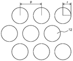
본 발명의 연마 재료에 사용될 수 있는 구조화된 표면이, 도 3a 내지 도 3g를 참조하면서, 예를 사용하여 기재된다. 도 3a는 삼각뿔 형상을 갖는 복수의 3차원 요소가 배치된 구조화된 표면의 상부 표면 개략도이다. 도 3a에서, 기호 o는 3차원 요소(12)의 기부의 길이를 나타내고, 기호 p는 3차원 요소(12)의 상단부 부분들 간의 거리를 나타낸다. 삼각뿔의 기부들의 길이는 서로 동일하거나 상이할 수 있고, 측부들의 길이는 서로 동일하거나 상이할 수 있다. 예를 들어, o는 대략 5 μm 이상 또는 대략 10 μm 이상, 및 대략 1000 μm 이하 또는 대략 500 μm 이하로 설정될 수 있다. p는 대략 5 μm 이상 또는 대략 10 μm 이상, 및 대략 1000 μm 이하 또는 대략 500 μm 이하로 설정될 수 있다. 도 3a에 예시되지 않지만, 3차원 요소(12)의 높이 h는 대략 2 μm 이상 또는 대략 4 μm 이상, 및 대략 600 μm 이하 또는 대략 300 μm 이하로 설정될 수 있다. h의 변화는 바람직하게는 3차원 요소(12)의 높이의 대략 20% 이하, 그리고 더 바람직하게는 대략 10% 이하이다.Structured surfaces that can be used in the abrasive material of the present invention are described by way of example with reference to Figures 3A-3G. 3A is a top surface schematic view of a structured surface in which a plurality of three-dimensional elements having a triangular pyramid shape are disposed. In Fig. 3A, the symbol o represents the length of the base of the three-
도 3b는 사각뿔 형상을 갖는 복수의 3차원 요소가 배치된 구조화된 표면의 상부 표면 개략도이다. 도 3b에서, 기호 o는 3차원 요소(12)의 기부의 길이를 나타내고, 기호 p는 3차원 요소(12)의 상단부 부분들 간의 거리를 나타낸다. 사각뿔의 기부들의 길이는 서로 동일하거나 상이할 수 있고, 측부들의 길이는 서로 동일하거나 상이할 수 있다. 예를 들어, o는 대략 5 μm 이상 또는 대략 10 μm 이상, 및 대략 1000 μm 이하 또는 대략 500 μm 이하로 설정될 수 있다. p는 대략 5 μm 이상 또는 대략 10 μm 이상, 및 대략 1000 μm 이하 또는 대략 500 μm 이하로 설정될 수 있다. 도 3b에 예시되지 않지만, 3차원 요소(12)의 높이 h는 대략 2 μm 이상 또는 대략 4 μm 이상, 및 대략 600 μm 이하 또는 대략 300 μm 이하로 설정될 수 있다. h의 변화는 바람직하게는 3차원 요소(12)의 높이의 대략 20% 이하, 그리고 더 바람직하게는 대략 10% 이하이다.3B is a top surface schematic view of a structured surface in which a plurality of three-dimensional elements having a quadrangular pyramidal shape are disposed. 3B, the symbol o represents the length of the base of the three-
본 발명의 다른 실시 형태에서, 3차원 요소는 절두형 삼각뿔 또는 절두형 사각뿔일 수 있다. 이러한 실시 형태의 3차원 요소의 상단부 표면은 일반적으로 연마 표면에 평행한 삼각형 또는 사각형 수평면으로 구성된다. 실질적으로 모든 상단부 표면이 바람직하게는 연마 층에 평행한 수평면 상에 존재한다.In another embodiment of the present invention, the three-dimensional element can be a truncated triangular pyramid or a truncated quadrangular pyramid. The upper end surface of the three-dimensional element of this embodiment generally consists of a triangular or rectangular horizontal surface parallel to the polishing surface. Substantially all upper end surfaces are preferably on a horizontal plane parallel to the polishing layer.
도 3c는 절두형 사각뿔을 갖는 복수의 3차원 요소가 배치된 구조화된 표면의 상부 표면 개략도이다. 상단부 부분을 절단하기 전의 사각뿔 형상이 왼쪽 상단에 예시된다. 도 3c에서, 기호 o는 3차원 요소(12)의 기부의 길이를 나타내고, 기호 u는 3차원 요소(12)의 기부들 간의 거리를 나타내고, 기호 y는 상단부 표면의 측부의 길이를 나타낸다. 절두형 사각뿔의 기부들의 길이는 서로 동일하거나 상이할 수 있고, 측부들의 길이는 서로 동일하거나 상이할 수 있고, 상단부 표면의 측부들의 길이는 서로 동일하거나 상이할 수 있다. 예를 들어, o는 대략 5 μm 이상 또는 대략 10 μm 이상, 및 대략 6000 μm 이하 또는 대략 3000 μm 이하로 설정될 수 있다. u는 0 μm 이상 또는 대략 2 μm 이상, 및 대략 10,000 μm 이하 또는 대략 5000 μm 이하로 설정될 수 있다. y는 대략 0.5 μm 이상 또는 대략 1 μm 이상, 및 대략 6000 μm 이하 또는 대략 3000 μm 이하로 설정될 수 있다. 도 3c에 예시되지 않지만, 3차원 요소(12)의 높이 h는 대략 5 μm 이상 또는 대략 10 μm 이상, 및 대략 10,000 μm 이하 또는 대략 5000 μm 이하로 설정될 수 있다. h의 변화는 바람직하게는 3차원 요소(12)의 높이의 대략 20% 이하, 그리고 더 바람직하게는 대략 10% 이하이다.3C is a top surface schematic view of a structured surface in which a plurality of three-dimensional elements having a truncated quadrangular pyramid are disposed. The shape of the quadrangular pyramid before cutting the upper part is illustrated in the upper left corner. 3C, the symbol o represents the length of the base of the three-
도 3d는 반구 형상을 갖는 복수의 3차원 요소가 배치된 구조화된 표면의 상부 표면 개략도이다. 도 3d에서, 기호 r은 3차원 요소(12)의 반경을 나타내고, 기호 p는 3차원 요소(12)들의 중앙 간의 거리를 나타낸다. 예를 들어, r은 대략 5 μm 이상 또는 대략 10 μm 이상, 및 대략 1000 μm 이하 또는 대략 500 μm 이하로 설정될 수 있다. p는 대략 5 μm 이상 또는 대략 10 μm 이상, 및 대략 1000 μm 이하 또는 대략 500 μm 이하로 설정될 수 있다. 도 3d에 예시되지 않지만, 반구 형상을 갖는 3차원 요소의 높이 h는 보통 반경 r과 동일하다. h의 변화는 바람직하게는 3차원 요소(12)의 높이의 대략 20% 이하, 그리고 더 바람직하게는 대략 10% 이하이다.FIG. 3D is a top surface schematic view of a structured surface in which a plurality of three-dimensional elements having a hemispherical shape are disposed. In Figure 3D, the symbol r represents the radius of the three-
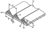
도 3e는 본 발명의 다른 실시 형태의 단면 개략도이고, 복수의 3차원 요소(12)는 측방향으로 배향된 삼각형 프리즘이고, 리지(ridge)를 갖는다. 3차원 요소(12)는 베이스 재료(15) 상에 배치되고, 연마 입자 및 결합제를 포함하는 연마 층 상부 부분(18)과, 결합제를 포함하지만 연마 입자를 포함하지 않는 연마 층 하부 부분(19)의 2층 구조로서 예시된다. 리지는 바람직하게는 실질적으로 연마 재료 전체를 가로질러 연마 층에 평행한 수평면 상에 있다. 일부 실시 형태에서, 실질적으로 모든 리지가 연마 층에 평행한 동일한 수평면 상에 존재한다. 도 3e에서, 기호 α는 3차원 요소(12)의 정각(vertical angle)을 나타내고; 기호 w는 3차원 요소(12)의 하단부 부분의 폭을 나타내고; 기호 p는 3차원 요소(12)의 상단부 부분들 간의 거리를 나타내고; 기호 u는 3차원 요소(12)의 긴 기부들 간의 거리를 나타내고; 기호 h는 베이스 재료(15)의 표면으로부터의 3차원 요소(12)의 높이를 나타내고; 기호 s는 연마 층 상부 부분(18)의 높이를 나타낸다. 예를 들어, α는 대략 30도 이상 또는 대략 45도 이상, 및 대략 150도 이하 또는 대략 140도 이하로 설정될 수 있다. w는 대략 2 μm 이상 또는 대략 4 μm 이상, 및 대략 2000 μm 이하 또는 대략 1000 μm 이하로 설정될 수 있다. p는 대략 2 μm 이상 또는 대략 4 μm 이상, 및 대략 4000 μm 이하 또는 대략 2000 μm 이하로 설정될 수 있다. u는 0 μm 이상 또는 대략 2 μm 이상, 및 대략 2000 μm 이하 또는 대략 1000 μm 이하로 설정될 수 있다. h는 대략 2 μm 이상 또는 대략 4 μm 이상, 및 대략 600 μm 이하 또는 대략 300 μm 이하로 설정될 수 있다. s는 3차원 요소(12)의 높이 h의 대략 5% 이상 또는 대략 10% 이상, 및 대략 95% 이하 또는 대략 90% 이하로 설정될 수 있다. h의 변화는 바람직하게는 3차원 요소(12)의 높이의 대략 20% 이하, 그리고 더 바람직하게는 대략 10% 이하이다.3E is a schematic cross-sectional view of another embodiment of the present invention, wherein the plurality of three-
도 3e에 예시된 개개의 3차원 요소(12)는 연마 재료의 표면 전체를 가로질러 연장될 수 있다. 이러한 경우, 3차원 요소(12)의 긴 기부 방향의 양 단부 부분은 연마 재료의 단부 부분 부근에 있고, 복수의 3차원 요소(12)는 밴드 형상으로 배치된다.The individual three-
본 발명의 다른 실시 형태에서, 3차원 요소는 모임 지붕 형상을 갖는다. 본 개시에서 "모임 지붕" 형상은 측부 표면이 2개의 대응하는 삼각형 형상 및 2개의 대응하는 사각형 형상으로 구성된 3차원 형상을 가리키며, 이때 인접한 삼각형 측부 표면과 사각형 측부 표면은 영역을 공유하고, 대응하는 2개의 사각형 측부 표면에 의해 공유되는 영역은 리지이다. 리지는 바람직하게는 실질적으로 연마 재료 전체를 가로질러 연마 층에 평행한 수평면 상에 있다. 일부 실시 형태에서, 실질적으로 모든 리지가 연마 층에 평행한 동일한 수평면 상에 존재한다. 2개의 삼각형 측부 표면과 2개의 사각형 측부 표면은 서로 동일한 형상 또는 상이한 형상을 가질 수 있다. 따라서, 모임 지붕 형상의 하단부 표면은 직사각형, 사다리꼴 등일 수 있고, 4개의 측부의 길이는 서로 상이한 정사각형 형상일 수 있다.In another embodiment of the present invention, the three-dimensional element has a gathered roof shape. In the present disclosure, the "meeting roof" shape refers to a three-dimensional shape in which the side surfaces consist of two corresponding triangular shapes and two corresponding rectangular shapes, wherein the adjacent triangular side surface and the square side surface share an area, The area shared by the two rectangular side surfaces is ridge. The ridges are preferably on a horizontal plane substantially parallel to the polishing layer across the entire polishing material. In some embodiments, substantially all of the ridges are on the same horizontal plane parallel to the polishing layer. The two triangular side surfaces and the two rectangular side surfaces may have the same shape or different shapes from each other. Thus, the lower end surface of the meeting roof shape may be rectangular, trapezoidal, or the like, and the four side portions may have a square shape that is different from each other.
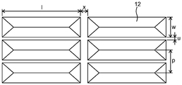
도 3f는 모임 지붕 형상을 갖는 복수의 3차원 요소가 배치된 구조화된 표면의 상부 표면 개략도이다. 도 3f는 직사각형 하단부 표면을 갖는 모임 지붕 형상을 예시한다. 도 3f에서, 기호 l은 3차원 요소(12)의 긴 기부의 길이를 나타내고, 기호 x는 인접한 3차원 요소(12)들의 짧은 기부들 간의 거리를 나타낸다. 예를 들어, l은 대략 5 μm 이상 또는 대략 10 μm 이상, 및 대략 10 mm 이하 또는 대략 5 mm 이하로 설정될 수 있다. x는 0 μm 이상 또는 대략 2 μm 이상, 및 대략 2000 μm 이하 또는 대략 1000 μm 이하로 설정될 수 있다. 기호 w, 기호 p 및 기호 u, 및 비록 도 3f에 예시되지 않지만 기호 h, 기호 s, 기호 α 등의 정의 및 예시적인 수치 범위는 도 3e에서 설명된 것과 동일하다.Figure 3f is a top surface schematic view of a structured surface on which a plurality of three-dimensional elements having a meeting roof shape are disposed. Figure 3f illustrates a meeting roof shape having a rectangular lower end surface. In Figure 3f, the symbol l represents the length of the long base of the three-
다른 실시 형태에서, 구조화된 표면은 다양한 형상을 갖는 복수의 3차원 요소의 조합을 포함한다. 도 3g는 그러한 실시 형태의 예를 예시한다. 도 3g에 예시된 구조화된 표면은 제1 삼각뿔(121), 제2 삼각뿔(122), 육각뿔(123) 및 모임 지붕(124)의 조합을 포함한다. 3차원 요소들 각각의 기부의 길이는 대략 5 μm 이상 또는 10 μm 이상, 및 대략 1000 μm 이하 또는 대략 500 μm 이하로 설정될 수 있고, 높이는 각각 대략 2 μm 이상 또는 대략 4 μm 이상, 및 대략 600 μm 이하 또는 대략 300 μm 이하로 설정될 수 있다. 인접한 3차원 요소들의 기부들 간의 거리는 0 μm 이상 또는 대략 2 μm 이상, 및 대략 10,000 μm 이하 또는 대략 5000 μm 이하로 설정될 수 있다. 모임 지붕(124)의 리지의 길이는 대략 0.5 μm 이상 또는 대략 1 μm 이상, 및 대략 1000 μm 이하 또는 대략 500 μm 이하로 설정될 수 있다.In another embodiment, the structured surface comprises a combination of a plurality of three-dimensional elements having various shapes. Figure 3g illustrates an example of such an embodiment. The structured surface illustrated in Figure 3G includes a combination of a first
몇몇 실시 형태에서, 연마 재료의 3차원 요소의 밀도, 다시 말하면, 연마 재료 1 ㎠당 3차원 요소의 개수는 대략 0.5개 요소/㎠ 이상 또는 1.0개 요소/㎠ 이상, 및 대략 1 × 10⁷개 요소/㎠ 이하 또는 대략 4 × 10⁶개 요소/㎠ 이하이다. 복수의 3차원 요소가 구조화된 표면 상에 체계적으로 배치된 실시 형태에서, 연마 재료 1 ㎠당 3차원 요소의 개수는 대략 0.05개 요소/㎠ 이상 또는 대략 0.10개 요소/㎠ 이상, 및 대략 1 × 10⁶개 요소/㎠ 이하 또는 대략 4 × 10⁵개 요소/㎠ 이하로 설정될 수 있다. 이러한 실시 형태에서, 3차원 요소를 구조화된 표면 상에 고 밀도로 배열함으로써 고 폴리싱 효율이 달성되는 반면, 슬러리, 연마 분말 등은, 예를 들어 홈과 같은, 3차원 요소들 사이에 존재하는 미리 결정된 패턴을 갖는 공간을 사용하고, 조합하여 구조화된 표면에 대해 표면 처리를 수행함으로써 효율적으로 방출될 수 있다.In some embodiments, the density of the three-dimensional elements of the abrasive material, in other words, the abrasive material 1, the number of three-dimensional elements are approximately 0.5-element / ㎠ or more or 1.0-element / ㎠ or more, and approximately 1 × 10 7 per ㎠ dog element / ㎠ or less is approximately 4 × 10 6-element / ㎠ below. In embodiments where a plurality of three-dimensional elements are systematically disposed on the structured surface, the number of three-dimensional elements per cm < 2 > of abrasive material may be greater than or equal to about 0.05 element / cm 2 or greater than or equal to about 0.10 elements / 10 6 elements / cm 2 or less or about 4 × 10 5 elements / cm 2 or less. In this embodiment, the high polishing efficiency is achieved by arranging the three-dimensional elements at high density on the structured surface, while slurry, abrasive powder, etc., Can be efficiently released by using a space having a determined pattern and performing surface treatment on the structured surface in combination.
본 발명의 연마 재료의 경우, 불소 처리 또는 규소 처리가 구조화된 표면의 적어도 일부에 대해 수행된다. 어떠한 이론에도 구애됨이 없이, 구조화된 표면이 다이아몬드-유사 탄소 등과 같은 표면 코팅 층에 의해 덮인 연마 재료, 및 연마 층이 연마 입자 및 수지 결합제를 포함하는 연마 재료는 구조화된 표면 상의 전하-증가(charge-up) 또는 구조화된 표면의 표면 에너지를 유발하는 것으로 여겨지며, 이에 따라 연마 입자가 전도성 Ni 도금 등에 의해 베이스 재료 상에 접착된 종래의 연마 재료와 비교해, 이물질이 정전기에 의해 또는 다른 상호작용에 의해 구조화된 표면에 매달리기 쉽다. 본 발명에 따르면, 구조화된 표면이 비교적 높은 밀도로 3차원 요소를 포함할지라도, 구조화된 표면의 표면 에너지는 이러한 3차원 요소의 표면 처리에 의해 감소될 수 있고, 이물질의 구조화된 표면 상에의 접착, 예컨대 연마 슬러리 중의 연마 입자, 유기 화합물 등, 폴리우레탄 폼 패드로부터 발생된 폴리우레탄 입자 등의 접착 또는 축적이 방지되거나 억제될 수 있다.In the case of the abrasive material of the present invention, a fluorine treatment or a silicon treatment is performed on at least a part of the structured surface. Without being bound by any theory, it is believed that an abrasive material wherein the structured surface is covered by a surface coating layer, such as diamond-like carbon, and an abrasive material wherein the abrasive layer comprises abrasive particles and resin binder, charge-up, or surface energy of the structured surface, and thus the abrasive particles are adhered to the base material by conductive Ni plating or the like, as compared to conventional abrasive materials where the abrasive particles are adhered to the base material by electrostatic or other interactions It is easy to hang on a structured surface. According to the present invention, even though the structured surface comprises three-dimensional elements at relatively high densities, the surface energy of the structured surface can be reduced by surface treatment of such three-dimensional elements, Adhesion or accumulation of abrasive particles, organic compounds, etc., in the polishing slurry, polyurethane particles generated from the polyurethane foam pad, etc., can be prevented or suppressed.
본 발명에서, 불소 처리는 플라즈마 처리, 화학 증착 (CVD) 방법, 물리 증착 (PVD) 방법 또는 불소 기체 처리에 의해 유리하게 수행될 수 있다.In the present invention, the fluorine treatment can be advantageously carried out by a plasma treatment, a chemical vapor deposition (CVD) method, a physical vapor deposition (PVD) method or a fluorine gas treatment.
본 발명에 따른 "플라즈마 처리"는 플라즈마에 의해 활성화된 원료 기체를 사용하여 처리될 물체의 표면의 화학 조성을 변화시키는 처리를 지칭하고, 처리될 물체로부터 유래된 재료를 비롯한 반응 생성물은 플라즈마 처리된 표면 상에 포함된다. 반면에, 화학 증착 및 물리 증착에서, 기체, 액체 또는 고체 원료로부터 유래된 성분을 포함하는 필름이 처리될 물체의 표면 상에 침착에 의해 형성된다. 화학 증착 방법에는, 예를 들어 열 CVD 방법, 직접 플라즈마 강화 CVD 방법, 원격 플라즈마 CVD 방법, 핫 와이어 CVD 방법 등이 포함된다. 물리 증착 방법에는 스퍼터링, 진공 침착, 아크 분무, 플라즈마 분무, 에어로졸 침착 방법 등이 포함된다."Plasma treatment" in accordance with the present invention refers to a treatment that changes the chemical composition of the surface of an object to be treated using a plasma activated source gas, and the reaction products, including materials derived from the object to be treated, Lt; / RTI > On the other hand, in chemical vapor deposition and physical vapor deposition, a film containing a component derived from a gas, liquid or solid raw material is formed by deposition on the surface of an object to be treated. The chemical vapor deposition method includes, for example, a thermal CVD method, a direct plasma enhanced CVD method, a remote plasma CVD method, a hot wire CVD method, and the like. Physical vapor deposition methods include sputtering, vacuum deposition, arc spraying, plasma spraying, aerosol deposition, and the like.
어떠한 이론에도 구애됨이 없이, 불소 처리는 불소가 표면 코팅 층, 예컨대 다이아몬드-유사 탄소 또는 연마 입자의 표면 주위에 도핑되는 것, 재료의 표면이 결합제에 포함된 중합체 중의 C-F 결합의 생성으로 인해 불소 종결되는 것, 많은 C-C 결합을 포함하는 고밀화 플루오로카본을 포함하는 코팅이 구조화된 표면 상에 형성되는 것 등과 같은 현상을 생성하는 것으로 여겨진다.Without wishing to be bound by any theory, fluorination can be achieved by the fact that fluorine is doped around the surface of a surface coating layer, such as diamond-like carbon or abrasive particles, because the surface of the material is fluorine It is believed that a coating comprising densified fluorocarbon containing many CC bonds is formed on the structured surface, and the like.
몇몇 실시 형태에서, 플라즈마 처리 또는 화학 증착 방법에 의한 불소 처리는 감압가능 챔버를 갖는 저압 플라즈마 장치 또는 대기압 플라즈마 장치를 사용하여 수행될 수 있다. 플라즈마 장치를 사용하는 화학 증착 방법은 일반적으로 플라즈마 강화 CVD 방법으로 지칭된다. 대기압 플라즈마 장치를 사용하는 경우, 불소-함유 기체 외에도, 질소 기체 및/또는 주기율표의 18족 원자, 구체적으로 헬륨, 네온, 아르곤, 크립톤, 제논, 라돈 등이 방전 기체로서 사용된다. 이들 중에서, 질소, 헬륨 및 아르곤이 유리하게 사용될 수 있고, 질소가 비용 관점에서 특히 유리하다. 저압 플라즈마 장치는 일반적으로 배치 처리(batch treating)에 사용된다. 긴 웨빙(webbing) 등의 연속 처리가 필요한 경우, 대기압 플라즈마 장치를 사용하는 것이 생산성 관점에서 유리할 수 있다. 종래의 방법, 예컨대 코로나 방전, 유전체 장벽 방전, 예컨대 13.56 ㎒ 고주파 전원을 사용하는 단일 또는 이중 RF 방전, 2.45 ㎓ 마이크로파 방전, 아크 방전 등이 플라즈마를 발생시키는 방법으로서 사용될 수 있다. 이러한 발생 방법 중에서, 13.56 ㎒ 고주파 전원을 사용하는 단일 RF 방전이 유리하게 사용될 수 있다.In some embodiments, fluorine treatment by plasma treatment or chemical vapor deposition methods may be performed using a low pressure plasma apparatus or an atmospheric pressure plasma apparatus having a decompressible chamber. A chemical vapor deposition method using a plasma apparatus is generally referred to as a plasma enhanced CVD method. When an atmospheric pressure plasma apparatus is used, in addition to the fluorine-containing gas, nitrogen gas and / or
플루오로카본, 예컨대 CF4, C4F8, C5F6, C4F6, CHF3, CH2F2, CH3F, C2F6, C3F8, C4F10, C6F14, 삼플루오르화질소 (NF3), SF6 등은 플라즈마 처리 또는 화학 증착 방법에서 사용되는 불소-함유 기체로서 사용될 수 있다. 안전성, 반응성 등의 관점에서, C3F8, C6F14 및 CF4가 유리하게 사용될 수 있다. 불소-함유 기체의 유량은 대략 20 sccm 이상 또는 대략 50 sccm 이상, 및 대략 1000 sccm 이하 또는 대략 500 sccm 이하로 설정될 수 있다. 대략 50 sccm 이상 및 대략 5000 sccm 이하의 유량을 갖는 캐리어 기체, 예컨대 질소, 헬륨 또는 아르곤이 장치에 공급되는 기체 유동에 추가로 포함될 수 있다.Fluorocarbons, such as CF 4, C 4 F 8, C 5 F 6, C 4 F 6, CHF 3, CH 2 F 2, CH 3 F, C 2 F 6, C 3 F 8, C 4
일부 실시 형태에서, 원료 기체 C/F 비(ratio)를 대략 3 이하로 설정함으로써 양호한 필름을 침착할 가능성이 알려져 있고, 이 경우, C/F 비는 비불소계 기체, 예컨대 아세틸렌, 아세톤 등을 첨가함으로써 조정될 수 있다. 원료 기체의 C/F 비가 대략 2 이상 및 대략 3 이하인 실시 형태에서, 바이어스 전압(bias voltage)에 따라, 플라즈마 처리로 인한 표면 개질이 우선적으로 발생할 수 있거나, 화학 증착 방법으로 인한 필름 침착이 우선적으로 발생할 수 있다. 그러한 실시 형태에서 바이어스 전압을 조정함으로써, 불소 처리는 플라즈마 처리 또는 화학 증착 또는 이들의 조합일 수 있다. 바이어스 전압의 범위는 장치의 크기 또는 설계 등에 기초해 다르지만, 일반적으로 대략 100 V 이하, 대략 0 V 이하 내지 대략 -1000 V 이상 또는 대략 -100,000 V 이상으로 설정될 수 있다.In some embodiments, it is known that a good film can be deposited by setting the raw gas C / F ratio to about 3 or less. In this case, the C / F ratio is determined by adding a non-fluorine gas such as acetylene, . In embodiments where the C / F ratio of the source gas is greater than or equal to about 2 and less than or equal to about 3, depending on the bias voltage, the surface modification due to the plasma treatment may occur preferentially or the film deposition due to the chemical vapor deposition process may preferentially Lt; / RTI > By adjusting the bias voltage in such an embodiment, the fluorine treatment can be plasma treatment or chemical vapor deposition or a combination thereof. The range of the bias voltage may vary depending on the size or design of the device, but may generally be set to about 100 V or less, about 0 V or less to about -1000 V or more, or about -100,000 V or more.
플라즈마 발생에 필요한 인가되는 전력은 처리될 연마 재료의 치수에 기초해 결정될 수 있고, 방전 공간 내의 전력 밀도는 일반적으로 대략 0.00003 W/㎠ 이상 또는 대략 0.0002 W/㎠ 이상, 및 대략 10 W/㎠ 이하 또는 대략 1 W/㎠ 이하로 선택될 수 있다. 예를 들어, 불소 처리될 연마 재료의 치수가 10 cm (길이) × 10 cm (폭) 이하인 경우, 인가되는 전력은 대략 200 W 이상 또는 대략 500 W 이상, 및 대략 4 kW 이하 또는 대략 2.5 kW 이하로 설정될 수 있다.The power applied for generating the plasma can be determined based on the dimensions of the abrasive material to be treated and the power density in the discharge space is generally about 0.00003 W / cm 2 or more, or about 0.0002 W / cm 2 or more, and about 10 W / Or about 1 W / cm < 2 > or less. For example, if the dimensions of the abrasive material to be fluorinated are less than or equal to 10 cm (length) x 10 cm (width), the applied power will be about 200 W or more, or about 500 W or more, and about 4 kW or less, or about 2.5 kW or less Lt; / RTI >
플라즈마 처리 또는 화학 증착 방법의 온도는 바람직하게는 처리될 연마 재료의 특징 및 성능 등을 손상시키지 않는 온도이고, 처리될 연마 재료의 표면 온도는 대략 -15℃ 이상, 대략 0℃ 이상 또는 대략 15℃ 이상, 및 대략 400℃ 이하, 대략 200℃ 이하 또는 대략 100℃ 이하로 설정될 수 있다. 연마 재료의 표면 온도는 연마 재료와 접촉하는 열전쌍, 방사 온도계 등에 의해 측정될 수 있다.The temperature of the plasma treatment or chemical vapor deposition process is preferably a temperature that does not impair the characteristics and performance of the polishing material to be treated and the like and the surface temperature of the polishing material to be treated is approximately -15 DEG C or higher, And about 400 캜 or less, about 200 캜 or less, or about 100 캜 or less. The surface temperature of the abrasive material can be measured by a thermocouple in contact with the abrasive material, a radiation thermometer, and the like.
저압 플라즈마 장치를 사용하는 플라즈마 처리 또는 화학 증착 방법을 수행할 때의 처리 압력은 대략 10 mTorr 이상 또는 대략 20 mTorr 이상, 및 대략 1500 mTorr 이하 또는 대략 1000 mTorr 이하로 설정될 수 있다.The processing pressure when performing a plasma treatment or chemical vapor deposition method using a low pressure plasma apparatus can be set to be about 10 mTorr or more, or about 20 mTorr or more, and about 1500 mTorr or less or about 1000 mTorr or less.
플라즈마 처리 또는 화학 증착 방법에 대한 처리 시간은 대략 2초 이상, 대략 5초 이상 또는 대략 10초 이상, 및 대략 300초 이하, 대략 180초 이하 또는 대략 120초 이하로 설정될 수 있다.The treatment time for the plasma treatment or chemical vapor deposition process can be set to about 2 seconds or more, about 5 seconds or more, or about 10 seconds or more, and about 300 seconds or less, about 180 seconds or less, or about 120 seconds or less.
다른 실시 형태에서, 원격 플라즈마 장치가 플라즈마 처리 또는 화학 증착 방법에 의한 불소 처리로서 사용될 수 있다. 원격 플라즈마 장치를 사용하는 화학 증착 방법은 일반적으로 원격 플라즈마 CVD 방법으로 지칭된다. 원격 플라즈마 장치에서, 플라즈마는 처리 챔버와는 상이한 플라즈마 여기 챔버 내에서 발생되고, 여기 활성종은 원료 기체를 플라즈마 여기 챔버 내에 도입시킴으로써 발생되고, 발생된 여기 활성종은 질소, 헬륨, 네온, 아르곤 등과 같은 캐리어 기체와 함께 처리 챔버 내로 유동되고, 이에 따라 연마 재료의 구조화된 표면의 불소 처리가 수행된다.In another embodiment, the remote plasma apparatus may be used as a fluorine treatment by a plasma treatment or a chemical vapor deposition method. Chemical vapor deposition methods using remote plasma devices are generally referred to as remote plasma CVD methods. In a remote plasma apparatus, the plasma is generated in a plasma excitation chamber that is different from the processing chamber, and the excited active species is generated by introducing the source gas into the plasma excitation chamber, and the excited active species generated is nitrogen, helium, neon, Is flowed into the processing chamber with the same carrier gas, thereby fluorinating the structured surface of the abrasive material.
감압 처리 챔버를 갖는 저압 원격 플라즈마 장치 또는 대기압 원격 플라즈마 장치가 원격 플라즈마 장치로서 사용될 수 있다. 사용될 수 있는 방전 기체 및 양호한 방전 기체는 저압 플라즈마 장치 및 대기압 플라즈마 장치에 대해 상기에 기재된 바와 같다. 고주파 (13.56 ㎒) RF 방전, 2.45 ㎓ 마이크로파 방전, 2.45 ㎓ 마이크로파 방전 / 전자 사이클로트론 공명(electron cyclotron resonance, ECR) 등이 일반적으로 플라즈마 발생 방법으로서 사용되고, 2.45 ㎓ 마이크로파 방전 및 2.45 ㎓ 마이크로파 방전 / 전자 사이클로트론 공명 (ECR)이 유리하게 사용되는데, 왜냐하면 원격 플라즈마에서 바람직한 높은 플라즈마 밀도가 달성될 수 있기 때문이다.A low pressure remote plasma apparatus or an atmospheric pressure remote plasma apparatus having a decompression chamber can be used as the remote plasma apparatus. The discharge gas and the preferred discharge gas that can be used are as described above for the low pressure plasma apparatus and the atmospheric pressure plasma apparatus. 2.45 ㎓ microwave discharge and 2.45 ㎓ microwave discharge / electron cyclotron resonance (ECR) are generally used as a plasma generation method and a 2.45 ㎓ microwave discharge and a 2.45 ㎓ microwave discharge / electron cyclotron The resonance (ECR) is advantageously used because the desired high plasma density in the remote plasma can be achieved.
플루오로카본, 예컨대 CF4, C4F8, C5F6, C4F6, CHF3, CH2F2, CH3F, C2F6, C3F8, C4F10, C6F14 등, 삼플루오르화질소 (NF3), SF6 등은 원격 플라즈마 장치를 사용하는 플라즈마 처리 또는 화학 증착 방법에서 사용되는 불소-함유 기체로서 사용될 수 있다. 여기 활성종의 수명이 더 길고, 안전성이 높으며, 이에 따라 NF3 및 SF6이 유리하게 사용될 수 있다. 불소-함유 기체의 유량은 대략 20 sccm 이상 또는 대략 50 sccm 이상, 및 대략 1000 sccm 이하 또는 대략 500 sccm 이하로 설정될 수 있다. 캐리어 기체의 유량은 대략 100 sccm 이상 또는 대략 200 sccm 이상, 및 대략 5000 sccm 이하 또는 대략 200 sccm 이하로 설정될 수 있다.Fluorocarbons, such as CF 4, C 4 F 8, C 5 F 6, C 4 F 6, CHF 3, CH 2 F 2, CH 3 F, C 2 F 6, C 3 F 8, C 4
일부 실시 형태에서, 원료 기체 C/F 비를 대략 3 이하로 설정함으로써 양호한 필름을 침착할 가능성이 알려져 있고, 이 경우, C/F 비는 비불소계 기체, 예컨대 아세틸렌, 아세톤 등을 첨가함으로써 조정될 수 있다. 원료 기체의 C/F 비가 대략 2 이상 및 대략 3 이하인 실시 형태에서, 바이어스 전압에 따라, 플라즈마 처리로 인한 표면 개질이 우선적으로 발생할 수 있거나, 화학 증착 방법으로 인한 필름 침착이 우선적으로 발생할 수 있다. 그러한 실시 형태에서 바이어스 전압을 조정함으로써, 불소 처리는 플라즈마 처리 또는 화학 증착 또는 이들의 조합일 수 있다. 바이어스 전압의 범위는 장치의 크기 또는 설계 등에 기초해 다르지만, 일반적으로 대략 100 V 이하, 대략 0 V 이하 내지 대략 -1000 V 이상 또는 대략 -100,000 V 이상으로 설정될 수 있다.In some embodiments, it is known that a good film can be deposited by setting the raw gas C / F ratio to about 3 or less. In this case, the C / F ratio can be adjusted by adding a non-fluorine based gas such as acetylene, have. In embodiments where the C / F ratio of the source gas is greater than or equal to about 2 and less than or equal to about 3, depending on the bias voltage, surface modification due to the plasma treatment may occur preferentially or film deposition due to the chemical vapor deposition process may occur preferentially. By adjusting the bias voltage in such an embodiment, the fluorine treatment can be plasma treatment or chemical vapor deposition or a combination thereof. The range of the bias voltage may vary depending on the size or design of the device, but may generally be set to about 100 V or less, about 0 V or less to about -1000 V or more, or about -100,000 V or more.
플라즈마 발생에 필요한 인가되는 전력은, 예를 들어 대략 1 W 이상 또는 대략 10 W 이상, 및 대략 300 kW 이하 또는 대략 30 kW 이하로 설정될 수 있다.The power required for generating the plasma can be set to, for example, about 1 W or more, or about 10 W or more, and about 300 kW or less or about 30 kW or less.
원격 플라즈마 장치에서, 불소 처리는 처리될 연마 재료를 저온에 유지하면서 수행될 수 있다. 예를 들어, 처리될 연마 재료의 표면 온도는 대략 -15℃ 이상, 대략 0℃ 이상 또는 대략 15℃ 이상, 및 대략 200℃ 이하, 대략 100℃ 이하 또는 대략 50℃ 이하로 설정될 수 있다. 연마 재료의 표면 온도는 연마 재료와 접촉하는 열전쌍, 방사 온도계 등에 의해 측정될 수 있다.In a remote plasma apparatus, the fluorine treatment can be performed while keeping the polishing material to be treated at a low temperature. For example, the surface temperature of the polishing material to be treated may be set at about -15 占 폚 or higher, about 0 占 폚 or higher, or about 15 占 폚 or higher, and about 200 占 폚 or lower, about 100 占 폚 or lower, or about 50 占 폚 or lower. The surface temperature of the abrasive material can be measured by a thermocouple in contact with the abrasive material, a radiation thermometer, and the like.
저압 원격 플라즈마 장치를 사용하는 플라즈마 처리 또는 화학 증착 방법을 수행할 때의 처리 압력은 대략 1 mTorr 이상 또는 대략 10 mTorr 이상, 및 대략 1500 mTorr 이하 또는 대략 1000 mTorr 이하로 설정될 수 있다.The process pressure when performing a plasma treatment or chemical vapor deposition process using a low pressure remote plasma apparatus may be set to be about 1 mTorr or more, or about 10 mTorr or more, and about 1500 mTorr or less or about 1000 mTorr or less.
플라즈마 처리 또는 화학 증착 방법에 대한 처리 시간은 대략 2초 이상, 대략 5초 이상 또는 대략 10초 이상, 및 대략 300초 이하, 대략 180초 이하 또는 대략 120초 이하로 설정될 수 있다.The treatment time for the plasma treatment or chemical vapor deposition process can be set to about 2 seconds or more, about 5 seconds or more, or about 10 seconds or more, and about 300 seconds or less, about 180 seconds or less, or about 120 seconds or less.
다른 실시 형태에서, 스퍼터링이 물리 증착 방법에 의한 불소 처리로서 사용될 수 있다. 스퍼터링은 전형적인 스퍼터링 장치, 예컨대 이온 스퍼터링 장치, DC 마그네트론 스퍼터링 장치, RF 마그네트론 스퍼터링 장치 등을 사용하여 수행될 수 있다.In another embodiment, sputtering can be used as the fluorine treatment by the physical vapor deposition method. Sputtering can be performed using a typical sputtering apparatus such as an ion sputtering apparatus, a DC magnetron sputtering apparatus, an RF magnetron sputtering apparatus, or the like.
플루오로중합체, 예컨대 폴리테트라플루오로에틸렌 (PTFE), 폴리비닐리덴 플루오라이드 (PVDF) 등이 불소 처리의 스퍼터링 타겟(target)으로서 사용될 수 있다. 플루오로카본, 예컨대 CF4, C4F8, C5F6, C4F6, CHF3, CH2F2, CH3F, C2F6, C3F8, C4F10, C6F14 등, 플루오르화질소 (NF3), SF6 등을 처리 챔버 내에 제공함으로써 반응성 스퍼터링이 수행될 수 있다.Fluoropolymers such as polytetrafluoroethylene (PTFE), polyvinylidene fluoride (PVDF) and the like can be used as a fluorine-treated sputtering target. Fluorocarbons, such as CF 4, C 4 F 8, C 5 F 6, C 4 F 6, CHF 3, CH 2 F 2, CH 3 F, C 2 F 6, C 3 F 8, C 4
스퍼터링 온도는 대략 -193℃ 이상 또는 대략 25℃ 이상, 및 대략 600℃ 이하 또는 대략 1300℃ 이하로 설정될 수 있다.The sputtering temperature may be set at about -193 ° C or higher, or about 25 ° C or higher, and about 600 ° C or lower, or about 1300 ° C or lower.
스퍼터링의 처리 압력은 대략 1 × 10⁻⁵ Torr 이상 또는 대략 1 × 10⁻³ Torr 이상, 및 대략 10 mTorr 이하 또는 대략 100 mTorr 이하로 설정될 수 있다.The processing pressure of the sputtering can be set to about 1 x 10⁻⁵ Torr or more, or about 1 x 10⁻³ Torr or more, and about 10 mTorr or less, or about 100 mTorr or less.
스퍼터링의 처리 시간은 대략 1초 이상, 대략 5초 이상 또는 대략 10초 이상, 및 대략 30초 이하, 대략 60초 이하 또는 대략 180초 이하로 설정될 수 있다.The processing time of the sputtering can be set to about 1 second or more, about 5 seconds or more, or about 10 seconds or more, and about 30 seconds or less, about 60 seconds or less, or about 180 seconds or less.
다른 실시 형태에서, 진공 침착이 물리 증착에 의한 불소 처리로서 사용될 수 있다. 진공 침착은 전형적인 침착 장치, 예컨대 저항 가열식 침착 장치, 전자 빔 침착 장치, 이온 도금 장치 등을 사용하여 수행될 수 있다.In another embodiment, vacuum deposition can be used as a fluorine treatment by physical vapor deposition. Vacuum deposition can be performed using a typical deposition apparatus, such as a resistance heating deposition apparatus, an electron beam deposition apparatus, an ion plating apparatus, or the like.
폴리테트라플루오로에틸렌 (PTFE), 폴리비닐리덴 플루오라이드 (PVDF) 및 다른 플루오로중합체, 플루오르화칼슘 (CaF2) 및 다른 불소-함유 유기 화합물 등이 침착 공급원으로서 사용될 수 있다.Polytetrafluoroethylene (PTFE), polyvinylidene fluoride (PVDF) and other fluoropolymers, calcium fluoride (CaF 2 ) and other fluorine-containing organic compounds may be used as deposition sources.
침착 온도는 대략 -193℃ 이상 또는 대략 25℃ 이상, 및 대략 600℃ 이하 또는 대략 1000℃ 이하로 설정될 수 있다.The deposition temperature may be set at about -193 DEG C or higher, or about 25 DEG C or higher, and about 600 DEG C or lower, or about 1000 DEG C or lower.
침착의 처리 압력은 대략 1 × 10⁻⁶ Torr 이상 또는 대략 1 × 10⁻⁵ Torr 이상, 및 대략 1 × 10⁻³ Torr 이하 또는 대략 1 × 10⁻² Torr 이하로 설정될 수 있다.The deposition processing pressure may be set to approximately 1 x 10⁻⁶ Torr or greater, or approximately 1 x 10⁻⁵ Torr or greater, and approximately 1 x 10⁻³ Torr or less, or approximately 1 x 10⁻² Torr or less.
침착의 처리 시간은 대략 5초 이상, 대략 10초 이상 또는 대략 30초 이상, 및 대략 120초 이하, 대략 600초 이하 또는 대략 1200초 이하로 설정될 수 있다.The treatment time for the deposition may be set to about 5 seconds or more, about 10 seconds or more, or about 30 seconds or more, and about 120 seconds or less, about 600 seconds or less, or about 1200 seconds or less.
다른 실시 형태에서, 불소 기체 (F2) 처리가 불소 처리로서 사용될 수 있다. 불소 기체는 질소, 헬륨, 아르곤, 이산화탄소 등과 같은 불활성 기체로 희석될 수 있고, 또한 희석 없이 있는 그대로 사용될 수 있다. 불소 기체 처리는 일반적으로 대기압에서 수행된다.In another embodiment, the fluorine gas (F 2 ) treatment can be used as the fluorine treatment. The fluorine gas may be diluted with an inert gas such as nitrogen, helium, argon, carbon dioxide, etc., and may be used as is without dilution. The fluorine gas treatment is generally carried out at atmospheric pressure.
불소 기체가 연마 재료의 구조화된 표면과 접촉될 때의 온도는 실온 이상, 대략 50℃ 이상 또는 대략 100℃ 이상, 및 대략 250℃ 이하, 대략 220℃ 이하 또는 대략 200℃ 이하로 설정될 수 있다.The temperature at which the fluorine gas is brought into contact with the structured surface of the abrasive material may be set to room temperature or higher, about 50 캜 or higher, or about 100 캜 or higher, and about 250 캜 or lower, about 220 캜 or lower or about 200 캜 or lower.
불소 기체 처리의 처리 시간은 대략 1분 이상 또는 대략 1시간 이상, 및 대략 1주 이하 또는 대략 50시간 이하로 설정될 수 있다.The treatment time of the fluorine gas treatment may be set to about 1 minute or more, or about 1 hour or more, and about 1 week or less or about 50 hours or less.
본 발명에서, 규소 처리는 플라즈마 처리, 화학 증착 방법, 물리 증착 방법 또는 원자 층 침착 방법에 의해 유리하게 수행될 수 있다. 어떠한 이론에도 구애됨이 없이, 규소 처리는 결합제에 포함된 중합체 중에 또는 연마 입자의 표면 또는 다이아몬드-유사 탄소 등과 같은 표면 코팅 상에 Si-O-Si 결합, Si-C-Si 결합, Si-O-C 결합 등을 형성함으로써 구조화된 표면이 개선되는 현상; Si-O-Si 결합, Si-C-Si 결합, Si-O-C 결합 등을 통해 형성된 비교적 밀도가 높은 네트워크 구조를 갖는 옥시탄화규소 또는 산화규소를 포함하는 코팅이 구조화된 표면 상에 형성되는 현상 등을 생성하는 것으로 여겨진다.In the present invention, the silicon treatment can be advantageously carried out by a plasma treatment, a chemical vapor deposition method, a physical vapor deposition method, or an atomic layer deposition method. Without wishing to be bound by any theory, it is believed that the silicon treatment can be carried out in the polymer contained in the binder or on the surface of abrasive particles or on a surface coating such as diamond-like carbon, Si-O-Si bonds, Si- A phenomenon in which the structured surface is improved by forming bonds or the like; A phenomenon in which a coating containing silicon oxycarbide or silicon oxide having a relatively dense network structure formed through Si-O-Si bonds, Si-C-Si bonds, Si-OC bonds or the like is formed on the structured surface ≪ / RTI >
플라즈마 처리 또는 화학 증착 방법에 의한 규소 처리는 앞서 기재된 불소 처리에 대해서와 동일한, 저압 플라즈마 장치, 대기압 플라즈마 장치, 저압 원격 플라즈마 장치, 대기압 원격 플라즈마 장치 등을 사용하여 수행될 수 있다. 방전 기체 및 플라즈마 발생 방법은 불소 처리에 대해 기재된 것과 동일하다.The silicon treatment by the plasma treatment or chemical vapor deposition method may be performed using the same low pressure plasma apparatus, atmospheric pressure plasma apparatus, low pressure remote plasma apparatus, atmospheric pressure remote plasma apparatus, and the like, which are the same as for the fluorine treatment described above. The discharge gas and the plasma generation method are the same as those described for the fluorine treatment.
실란 (SiH4), 테트라메틸실란 (TMS), 헥사메틸다이실록산 (HMDSO), 헥사메틸다이실라잔 (HMDS), 테트라에톡시실란 (TEOS) 등이 플라즈마 처리 또는 화학 증착 방법에 사용되는 불소-함유 기체로서 사용될 수 있다. 이들 중에서, 모노실란 또는 테트라메틸실란이 반응성이 높고 확산 계수가 크기 때문에 유리하게 사용될 수 있다. 대기압 플라즈마 장치가 사용되는 경우, 저 비등점을 갖고 비가연성인 테트라메틸실란이 사용된다. 규소-함유 기체의 유량은 대략 20 sccm 이상 또는 대략 50 sccm 이상, 및 대략 1000 sccm 이하 또는 대략 500 sccm 이하로 설정될 수 있다. 대략 50 sccm 이상 및 대략 5000 sccm 이하의 유량을 갖는 캐리어 기체, 예컨대 질소, 헬륨 또는 아르곤이 장치에 공급되는 기체 유동에 추가로 포함될 수 있다.A fluorine-containing gas such as silane (SiH 4 ), tetramethylsilane (TMS), hexamethyldisiloxane (HMDSO), hexamethyldisilazane (HMDS), tetraethoxysilane (TEOS) Containing gas. Among them, monosilane or tetramethylsilane can be advantageously used because of high reactivity and large diffusion coefficient. When an atmospheric plasma apparatus is used, tetramethylsilane, which has low boiling point and is nonflammable, is used. The flow rate of the silicon-containing gas may be set at about 20 sccm or more, or about 50 sccm or more, and about 1000 sccm or less, or about 500 sccm or less. A carrier gas, such as nitrogen, helium, or argon, having a flow rate of about 50 sccm or more and a flow rate of about 5000 sccm or less may be further included in the gas flow fed to the apparatus.
산소 원자가 규소-함유 기체에 포함되지 않는 경우, 산소가 플라즈마 장치에 공급되는 기체 유동에 첨가된다. 산소는 규소-함유 기체와는 별개의 라인을 통해 플라즈마 장치의 챔버 내로 공급될 수 있거나, 챔버 내에 배치된 샤워헤드(showerhead)를 통해 규소-함유 기체와 함께 혼합 기체로서 공급될 수 있다. 산소의 유량은 대략 5 sccm 이상 또는 대략 10 sccm 이상, 및 대략 500 sccm 이하 또는 대략 300 sccm 이하로 설정될 수 있다. 규소-함유 기체의 유량이 1로 설정된 상태에서, 산소와 규소-함유 기체의 유량 비는 대략 0.1:1 이상, 대략 0.2:1 이상 또는 대략 0.3:1 이상, 및 대략 5:1 이하, 대략 4:1 이하 또는 대략 3:1 이하로 설정될 수 있다. 규소-함유 기체의 공급을 중단한 후, 예를 들어 대략 5 sccm 이상 또는 대략 10 sccm 이상, 및 대략 500 sccm 이하 또는 대략 300 sccm 이하의 유량으로 오직 산소만을 공급함으로써 후처리가 수행될 수 있다.When the oxygen atom is not included in the silicon-containing gas, oxygen is added to the gas flow supplied to the plasma apparatus. Oxygen may be fed into the chamber of the plasma apparatus through a line separate from the silicon-containing gas, or may be supplied as a gaseous mixture with the silicon-containing gas through a showerhead disposed within the chamber. The flow rate of oxygen can be set to about 5 sccm or more, or about 10 sccm or more, and about 500 sccm or less, or about 300 sccm or less. The flow rate ratio of oxygen to the silicon-containing gas is about 0.1: 1 or more, about 0.2: 1 or more, or about 0.3: 1 or more, and about 5: 1 or less, about 4 : 1 or less or about 3: 1 or less. After the supply of the silicon-containing gas is stopped, the post-treatment can be performed, for example, by supplying only oxygen at a flow rate of, for example, about 5 sccm or more, or about 10 sccm or more, and about 500 sccm or less or about 300 sccm or less.
플라즈마 발생에 필요한 인가되는 전력은 처리될 연마 재료의 치수에 기초해 결정될 수 있고, 방전 공간 내의 전력 밀도는 일반적으로 대략 0.00003 W/㎠ 이상 또는 대략 0.0002 W/㎠ 이상, 및 대략 10 W/㎠ 이하 또는 대략 1 W/㎠ 이하로 선택될 수 있다. 예를 들어, 규소 처리될 연마 재료의 치수가 10 cm (길이) × 10 cm (폭) 이하인 경우, 인가되는 전력은 대략 1 W 이상 또는 대략 10 W 이상, 및 대략 300 kW 이하 또는 대략 30 kW 이하로 설정될 수 있다.The power applied for generating the plasma can be determined based on the dimensions of the abrasive material to be treated and the power density in the discharge space is generally about 0.00003 W / cm 2 or more, or about 0.0002 W / cm 2 or more, and about 10 W / Or about 1 W / cm < 2 > or less. For example, when the dimensions of the abrasive material to be siliconized are less than or equal to 10 cm (length) x 10 cm (width), the applied power is approximately 1 W or more, or approximately 10 W or more, and approximately 300 kW or less, or approximately 30 kW or less Lt; / RTI >
플라즈마 처리 또는 화학 증착 방법의 온도는 바람직하게는 처리될 연마 재료의 특징 및 성능 등을 손상시키지 않는 온도이고, 처리될 연마 재료의 표면 온도는 대략 -15℃ 이상, 대략 0℃ 이상 또는 대략 15℃ 이상, 및 대략 400℃ 이하, 대략 200℃ 이하 또는 대략 100℃ 이하로 설정될 수 있다. 연마 재료의 표면 온도는 연마 재료와 접촉하는 열전쌍, 방사 온도계 등에 의해 측정될 수 있다.The temperature of the plasma treatment or chemical vapor deposition process is preferably a temperature that does not impair the characteristics and performance of the polishing material to be treated and the like and the surface temperature of the polishing material to be treated is approximately -15 DEG C or higher, And about 400 캜 or less, about 200 캜 or less, or about 100 캜 or less. The surface temperature of the abrasive material can be measured by a thermocouple in contact with the abrasive material, a radiation thermometer, and the like.
저압 플라즈마 장치를 사용하는 플라즈마 처리 또는 화학 증착 방법을 수행할 때의 처리 압력은 대략 10 mTorr 이상 또는 대략 20 mTorr 이상, 및 대략 1500 mTorr 이하 또는 대략 1000 mTorr 이하로 설정될 수 있다.The processing pressure when performing a plasma treatment or chemical vapor deposition method using a low pressure plasma apparatus can be set to be about 10 mTorr or more, or about 20 mTorr or more, and about 1500 mTorr or less or about 1000 mTorr or less.
플라즈마 처리 또는 화학 증착 방법에 대한 처리 시간은 대략 2초 이상, 대략 5초 이상 또는 대략 10초 이상, 및 대략 300초 이하, 대략 180초 이하 또는 대략 120초 이하로 설정될 수 있다.The treatment time for the plasma treatment or chemical vapor deposition process can be set to about 2 seconds or more, about 5 seconds or more, or about 10 seconds or more, and about 300 seconds or less, about 180 seconds or less, or about 120 seconds or less.
다른 실시 형태에서, 스퍼터링 또는 진공 침착이 물리 증착에 의한 규소 처리로서 사용될 수 있다. 물리 증착 방법을 사용하는 규소 처리는 표준 스퍼터링 장비, 예컨대 불소 처리에 대해 기재된 동일한 이온 스퍼터링 장비, DC 마그네트론 스퍼터링 장비, RF 마그네트론 스퍼터링 장비 등, 또는 표준 증착 장비, 예컨대 저항 가열식 증착 장비, 전자 빔 증착 장비, 이온 도금 장비 등을 사용하여 수행될 수 있다.In another embodiment, sputtering or vacuum deposition may be used as silicon treatment by physical vapor deposition. The silicon treatment using the physical vapor deposition method can be carried out using standard sputtering equipment, such as the same ion sputtering equipment described for fluorine treatment, DC magnetron sputtering equipment, RF magnetron sputtering equipment, or standard deposition equipment such as resistance heating deposition equipment, electron beam deposition equipment , Ion plating equipment, and the like.
규소 처리의 스퍼터링 타겟은 이산화규소 (SiO2)일 수 있다. 반응성 스퍼터링은 규소 (Si)를 스퍼터링 타겟으로서 사용할 경우 산소를 처리 챔버 내로 공급함으로써 수행될 수 있다.The sputtering target of the silicon treatment may be silicon dioxide (SiO 2 ). Reactive sputtering can be performed by supplying oxygen into the processing chamber when silicon (Si) is used as a sputtering target.
스퍼터링 온도는 대략 -193℃ 이상 또는 대략 25℃ 이상, 및 대략 600℃ 이하 또는 대략 1300℃ 이하로 설정될 수 있다.The sputtering temperature may be set at about -193 ° C or higher, or about 25 ° C or higher, and about 600 ° C or lower, or about 1300 ° C or lower.
스퍼터링의 처리 압력은 대략 1 × 10⁻⁵ Torr 이상 또는 대략 1 × 10⁻³ Torr 이상, 및 대략 10 mTorr 이하 또는 대략 100 mTorr 이하로 설정될 수 있다.The processing pressure of the sputtering can be set to about 1 x 10⁻⁵ Torr or more, or about 1 x 10⁻³ Torr or more, and about 10 mTorr or less, or about 100 mTorr or less.
스퍼터링의 처리 시간은 대략 1초 이상, 대략 5초 이상 또는 대략 10초 이상, 및 대략 30초 이하, 대략 60초 이하 또는 대략 180초 이하로 설정될 수 있다.The processing time of the sputtering can be set to about 1 second or more, about 5 seconds or more, or about 10 seconds or more, and about 30 seconds or less, about 60 seconds or less, or about 180 seconds or less.
이산화규소 (SiO2)는 진공 증착의 증착 공급원으로서 사용될 수 있다. 전자 빔 증착은 이산화규소 증착과 함께 유리하게 사용될 수 있다. 규소 처리는 증착 공급원으로서 일산화규소 (SiO)를 사용한 후 산화 분위기에서 어닐링(annealing) 산화를 수행하는 증착, 및 증착 챔버 내로 산소 플라즈마를 도입하면서 일산화규소를 증착하는 것에 의해 수행될 수 있다.Silicon dioxide (SiO 2 ) can be used as a deposition source for vacuum deposition. Electron beam deposition can be advantageously used with silicon dioxide deposition. Silicon treatment can be performed by depositing silicon monoxide (SiO) as a deposition source, followed by deposition to perform annealing oxidation in an oxidizing atmosphere, and deposition of silicon monoxide while introducing an oxygen plasma into the deposition chamber.
침착 온도는 대략 -193℃ 이상 또는 대략 25℃ 이상, 및 대략 600℃ 이하 또는 대략 1000℃ 이하로 설정될 수 있다.The deposition temperature may be set at about -193 DEG C or higher, or about 25 DEG C or higher, and about 600 DEG C or lower, or about 1000 DEG C or lower.
침착의 처리 압력은 대략 1 × 10⁻⁶ Torr 이상 또는 대략 1 × 10⁻⁵ Torr 이상, 및 대략 1 × 10⁻³ Torr 이하 또는 대략 1 × 10⁻² Torr 이하로 설정될 수 있다.The deposition processing pressure may be set to approximately 1 x 10⁻⁶ Torr or greater, or approximately 1 x 10⁻⁵ Torr or greater, and approximately 1 x 10⁻³ Torr or less, or approximately 1 x 10⁻² Torr or less.
침착의 처리 시간은 대략 5초 이상, 대략 10초 이상 또는 대략 30초 이상, 및 대략 120초 이하, 대략 600초 이하 또는 대략 1200초 이하로 설정될 수 있다.The treatment time for the deposition may be set to about 5 seconds or more, about 10 seconds or more, or about 30 seconds or more, and about 120 seconds or less, about 600 seconds or less, or about 1200 seconds or less.
다른 실시 형태에서, 원자 층 침착(atom layer deposition) 방법 (ALD)이 규소 처리로서 사용될 수 있다. 원자 층 침착 방법은 적어도 2가지 유형의 전구체 기체를 반응 챔버 내로 교대로 제공하는 단계, 이러한 전구체 기체의 단일 층을 매번 구조화된 표면 상에 침착하는 단계, 및 이러한 전구체 기체를 구조화된 표면 상에서 반응시키는 단계를 포함한다.In another embodiment, an atom layer deposition (ALD) method may be used as the silicon treatment. The atomic layer deposition method comprises providing at least two types of precursor gases alternately into the reaction chamber, depositing a single layer of such precursor gas on the structured surface each time, and reacting such precursor gas on the structured surface .
사용될 수 있는 전구체 기체 A의 예에는 테트라에톡시실란, 비스 (tert-부톡시) (아이소프로폭시) 실란올, 비스 (아이소프로폭시) (tert-부톡시) 실란올, 비스 (tert-펜톡시) (아이소프로폭시) 실란올, 비스 (아이소프로폭시) (tert-펜톡시) 실란올, 비스 (tert-펜톡시) (tert-부톡시) 실란올, 비스 (tert-부톡시) (tert-펜톡시) 실란올, 트리스 (tert-펜톡시) 실란올 등이 포함된다. 전구체 기체 B의 예에는 물 (H2O), 산소 (O2), 오존 (O3) 등이 포함된다.Examples of the precursor gas A that can be used include tetraethoxysilane, bis (tert-butoxy) (isopropoxy) silanol, bis (isopropoxy) (tert-butoxy) silanol, bis (Tert-butoxy) silanol, bis (tert-butoxy) silanol, bis (tert-butoxy) Pentoxy) silanol, tris (tert-pentoxy) silanol, and the like. Examples of precursor gas B include water (H 2 O), oxygen (O 2 ), ozone (O 3 ), and the like.
전구체 기체 A의 유량은 대략 0.1 sccm 이상 또는 대략 1 sccm 이상, 및 대략 100 sccm 이하 또는 대략 1000 sccm 이하로 설정될 수 있다. 전구체 기체 A를 반응 챔버로 도입시키는 시간은 대략 0.01초 이상 또는 대략 0.1초 이상, 및 대략 10초 이하 또는 대략 100초 이하 동안일 수 있다.The flow rate of the precursor gas A may be set to be about 0.1 sccm or more, or about 1 sccm or more, and about 100 sccm or less or about 1000 sccm or less. The time for introducing the precursor gas A into the reaction chamber may be about 0.01 seconds or more, or about 0.1 seconds or more, and about 10 seconds or less or about 100 seconds or less.
전구체 기체 B의 유량은 대략 0.1 sccm 이상 또는 대략 1 sccm 이상, 및 대략 100 sccm 이하 또는 대략 1000 sccm 이하로 설정될 수 있다. 전구체 기체 B를 반응 챔버로 도입시키는 시간은 대략 0.01초 이상 또는 대략 0.1초 이상, 및 대략 10초 이하 또는 대략 100초 이하 동안일 수 있다.The flow rate of the precursor gas B may be set at about 0.1 sccm or more, or about 1 sccm or more, and about 100 sccm or less, or about 1000 sccm or less. The time for introducing the precursor gas B into the reaction chamber may be about 0.01 seconds or more, or about 0.1 seconds or more, and about 10 seconds or less or about 100 seconds or less.
미반응된 전구체 기체 및/또는 반응 부산물은 전구체 기체 A의 도입과 전구체 기체 B의 도입 사이에 퍼지 기체를 반응 챔버 내로 도입시킴으로써 반응 챔버로부터 퍼징될 수 있다. 퍼지 기체는 전구체 기체와 반응하지 않을 불활성 기체이다. 사용될 수 있는 퍼지 기체의 예에는 질소 기체, 헬륨, 네온, 아르곤 및 이들의 혼합물이 포함된다. 퍼지 기체의 유량은, 예를 들어 대략 10 sccm 이상 또는 대략 50 sccm 이상, 및 대략 500 sccm 이하 또는 대략 1000 sccm 이하일 수 있고, 퍼지 기체의 도입 시간은 대략 1초 이상 또는 대략 10초 이상, 및 대략 30초 이하 또는 대략 60초 이하일 수 있다.Unreacted precursor gas and / or reaction by-products may be purged from the reaction chamber by introducing purge gas into the reaction chamber between introduction of the precursor gas A and introduction of the precursor gas B. The purge gas is an inert gas that will not react with the precursor gas. Examples of purge gases that may be used include nitrogen gas, helium, neon, argon, and mixtures thereof. The flow rate of the purge gas may be, for example, about 10 sccm or more, or about 50 sccm or more, and about 500 sccm or less or about 1000 sccm or less, and the introduction time of the purge gas may be about 1 second or more, 30 seconds or less, or about 60 seconds or less.
미리 결정된 두께의 옥시탄화규소 또는 산화규소를 포함하는 필름은 전구체 기체 A 및 전구체 기체 B를 도입하는 횟수뿐만 아니라 전구체 기체 A 및 전구체 기체 B의 유량 및 도입 시간을 변경함으로써 구조화된 표면 상에 형성될 수 있다. 전구체 기체 A 및/또는 전구체 기체 B를 도입한 후, 전구체 기체 A와 전구체 기체 B 간의 반응은 열, 플라즈마, 펄스 플라즈마, 헬리콘 플라즈마, 고밀도 플라즈마, 유도성 결합 플라즈마, X-선, 전자 빔, 광자, 원격 플라즈마 등을 사용하여 촉진될 수 있다.A film of silicon carbide or silicon oxide having a predetermined thickness is formed on the structured surface by changing the flow rate and the introduction time of the precursor gas A and the precursor gas B as well as the number of times of introducing the precursor gas A and the precursor gas B . After introducing precursor gas A and / or precursor gas B, the reaction between precursor gas A and precursor gas B can be performed in a variety of ways including, but not limited to, heat, plasma, pulsed plasma, helion plasma, high density plasma, inductive coupled plasma, X- Photons, remote plasmas, and the like.
이러한 방식으로 표면 처리된 구조화된 표면의 물리적 특성은, 예를 들어 접촉각, 경도 등에 의해 평가될 수 있다.The physical properties of structured surfaces that have been surface treated in this manner can be assessed, for example, by contact angles, hardness, and the like.
몇몇 실시 형태에서, 예를 들어 구조화된 표면이 불소 처리된 실시 형태에서, 표면 처리된 구조화된 표면의 물 접촉각은 대략 70° 이상 또는 대략 90° 이상, 및 대략 120° 이하 또는 대략 150°이하였다. 물 접촉각은 소적(droplet) 방법, 팽창/수축 방법, 빌헬미(Wilhelmy) 방법 등에 의해 결정될 수 있다.In some embodiments, for example, in a structured surface fluorinated embodiment, the water contact angle of the surface treated structured surface is greater than or equal to about 70 degrees, or greater than or equal to about 90 degrees, and less than or equal to about 120 degrees or less than or equal to about 150 degrees . The water contact angle can be determined by a droplet method, an expansion / contraction method, a Wilhelmy method, and the like.
다른 몇몇 실시 형태에서, 예를 들어 구조화된 표면이 친수성 표면을 제공하도록 규소 처리된 실시 형태에서, 표면 처리된 구조화된 표면의 물 접촉각은 대략 0° 이상 또는 대략 10° 이상, 및 대략 30° 이하 또는 대략 45° 이하였다. 물 접촉각은 소적 방법, 팽창/수축 방법, 빌헬미 방법 등에 의해 결정될 수 있다.In some other embodiments, for example, in embodiments wherein the structured surface is siliconized to provide a hydrophilic surface, the water contact angle of the surface treated structured surface may be greater than or equal to about 0 or greater than or equal to about 10, and less than or equal to about 30 Or about 45 degrees or less. The water contact angle can be determined by a droplet method, an expansion / contraction method, a Bill Helmi method, and the like.
다른 실시 형태에서, 표면 처리된 구조화된 표면의 경도는, 쇼어(Shore) 경도로 변환할 경우, 대략 40 이상 또는 대략 50 이상, 및 대략 87 이하 또는 대략 97 이하였다. 표면 처리된 구조화된 표면의 경도는, 예를 들어 나노 압입(nano indentation) 방법에 의해 결정될 수 있다. 쇼어 경도로서 계산될 때 표면 처리된 구조화된 표면의 경도가 대략 50 이상인 경우, 비교적 연질인 이물질, 예컨대 폴리우레탄의 중합체 입자 등의 구조화된 표면에의 접착이 방지될 수 있다.In another embodiment, the hardness of the surface treated structured surface is greater than or equal to about 40 or greater than about 50, and less than or equal to about 87 or less than or equal to about 97 when converted to Shore hardness. The hardness of the surface-treated structured surface can be determined, for example, by the nano indentation method. When the hardness of the surface-treated structured surface is about 50 or more when calculated as the Shore hardness, adhesion to a structured surface of relatively soft foreign matter, such as polymer particles of polyurethane, can be prevented.
구조화된 표면 또는 불소 처리되거나 규소 처리된 개질된 상태의 구조화된 표면 상에 침착된 필름의 조성은 x-선 광전자 분광법 (XPS), 또는 비행 시간을 사용하는 2차 이온 질량 분광법 (TOF-SIMS) 등을 사용하여 정성적으로 또는 정량적으로 평가될 수 있다. XPS 스펙트럼은, 예를 들어 표면에 대해 90°의 전자 방출 편각에서 단색 Al K α 광자 공급원을 사용하는 크라토스 액시스 울트라 분광계(Kratos Axis Ultra spectrometer)를 사용하여 획득될 수 있다. TOF-SIMS는, 예를 들어 빔 직경이 대략 1 μm인 400 × 400 마이크로미터 면적에 의해 래스터화된(rasterized) 펄스 25 keV Ga+ 1차 이온 빔을 사용할 수 있다.The composition of the film deposited on a structured surface or a structured surface in a fluorinated or silicon-treated modified state can be determined by x-ray photoelectron spectroscopy (XPS), or secondary ion mass spectrometry (TOF-SIMS) And the like can be evaluated qualitatively or quantitatively. The XPS spectrum can be obtained, for example, using a Kratos Axis Ultra spectrometer using a monochromatic Al K alpha photon source at an electron emission angle of 90 [deg.] To the surface. The TOF-SIMS can use a rasterized pulse 25 keV Ga + primary ion beam, for example, with a 400 x 400 micrometer area with a beam diameter of approximately 1 μm.
본 발명의 또 다른 실시 형태는 상부에 배열된 복수의 3차원 요소를 갖도록 구성된 구조화된 표면을 가진 연마 층을 포함하는 연마 재료로서, 구조화된 표면의 적어도 일부는, (a) 고밀화 플루오로카본, 옥시탄화규소, 및 산화규소로 이루어진 군으로부터 선택되는 재료를 포함하는 필름; (b) 불소 종결된 표면; 또는 (c) 이들의 조합을 포함하는, 연마 재료를 제공한다.Another embodiment of the present invention is an abrasive material comprising an abrasive layer having a structured surface configured to have a plurality of three-dimensional elements arranged thereon, wherein at least a portion of the structured surface comprises: (a) densified fluorocarbon, A film comprising a material selected from the group consisting of silicon oxycarbide, silicon oxycarbide, and silicon oxide; (b) a fluorine terminated surface; Or (c) a combination thereof.
본 발명에서, "고밀화 플루오로카본"은 비교적 많은 양의 4차 탄소 원자를 포함하는 결과로서 C-C 결합을 갖도록 형성된 밀도가 높은 3차원 네트워크 구조를 포함하는 플루오로카본 재료를 지칭한다. 고밀화 플루오로카본은, 가교결합되거나 가교결합되지 않은 표준 플루오로중합체에 비해, 고 경도 및 뛰어난 내마모성 및 이물질 내접착성을 갖는다.In the present invention, "densified fluorocarbon" refers to a fluorocarbon material comprising a dense three dimensional network structure formed to have C-C bonds as a result of containing a relatively large amount of quaternary carbon atoms. The densified fluorocarbons have high hardness and excellent abrasion resistance and adhesion in foreign matter, compared with standard fluoropolymers that are not crosslinked or crosslinked.
고밀화 플루오로카본은 탄소 및 불소 외에도 수소, 산소, 질소 등과 같은 다른 원자를 포함할 수 있다. 몇몇 실시 형태에서, 고밀화 플루오로카본은 수소 이외의 원소들의 총량을 기준으로 대략 20 원자% 이상 또는 대략 25 원자% 이상, 및 대략 65 원자% 이하 또는 대략 60 원자% 이하의 탄소 원자를 포함한다. 다른 몇몇 실시 형태에서, 고밀화 플루오로카본은 수소 이외의 원소들의 총량을 기준으로 대략 30 원자% 이상 또는 대략 35 원자% 이상, 및 대략 75 원자% 이하 또는 대략 70 원자% 이하의 탄소 원자를 포함한다. 더욱이, 다른 몇몇 실시 형태에서, 고밀화 플루오로카본은 수소 이외의 원소들의 총량을 기준으로 대략 25 원자% 이상 또는 대략 30 원자% 이상, 및 대략 80 원자% 이하 또는 대략 70 원자% 이하의 4개의 인접한 탄소 원자에 결합된 4차 탄소 원자를 포함한다. 고밀화 플루오로카본의 탄소 원자 및 불소 원자의 원자 백분율은, 예를 들어 XPS를 사용하여 결정될 수 있고, 4차 탄소 원자의 원자 백분율은, 예를 들어 13C-NMR 등을 사용하여 결정될 수 있다.The densified fluorocarbon may contain other atoms such as hydrogen, oxygen, nitrogen, etc. in addition to carbon and fluorine. In some embodiments, the densified fluorocarbon comprises about 20 atomic percent or more, or about 25 atomic percent or more, and about 65 atomic percent or less or about 60 atomic percent or less of carbon atoms based on the total amount of elements other than hydrogen. In some other embodiments, the densified fluorocarbon comprises about 30 atomic percent or more, or about 35 atomic percent or more, and about 75 atomic percent or less, or about 70 atomic percent or less of carbon atoms, based on the total amount of elements other than hydrogen . Moreover, in some other embodiments, the densified fluorocarbon is present in an amount of at least about 25 atomic percent, or at least about 30 atomic percent, and no more than about 80 atomic percent or no more than about 70 atomic percent based on the total amount of the elements other than hydrogen, And a quaternary carbon atom bonded to the carbon atom. The atomic percentages of carbon atoms and fluorine atoms of the densified fluorocarbons can be determined, for example, using XPS, and the atomic percentages of the quaternary carbon atoms can be determined using, for example, 13 C-NMR.
옥시탄화규소는 규소, 산소 및 탄소를 포함하지만 3차원 원소인 다른 원자, 예를 들어 수소, 질소 등을 포함할 수 있는 화합물이다. 옥시탄화규소는 경질이고, 뛰어난 내마모성, 이물질 내접착성 등을 갖고, 조성을 변화시킴으로써 친수성 또는 소수성으로 만들어질 수 있다. 몇몇 실시 형태에서, 옥시탄화규소는 수소 이외의 원소들의 총량을 기준으로 대략 10 원자% 이상 또는 대략 15 원자% 이상, 및 대략 90 원자% 이하 또는 대략 80 원자% 이하의 규소 원자를 함유한다. 다른 몇몇 실시 형태에서, 옥시탄화규소는 수소 이외의 원소들의 총량을 기준으로 대략 5 원자% 이상 또는 대략 10 원자% 이상, 및 대략 80 원자% 이하 또는 대략 70 원자% 이하의 산소 원자를 함유한다. 더욱이, 다른 몇몇 실시 형태에서, 옥시탄화규소는 수소 이외의 원소들의 총량을 기준으로 대략 1 원자% 이상 또는 대략 5 원자% 이상, 및 대략 90 원자% 이하 또는 대략 80 원자% 이하의 탄소 원자를 함유한다. 옥시탄화규소 내의 규소 원자, 산소 원자 및 탄소 원자의 원자 백분율은 XPS, TOF-SIOMS 등을 사용하여 결정될 수 있다.The silicon oxycarbide is a compound that includes silicon, oxygen, and carbon but may include other atoms that are three-dimensional elements, such as hydrogen, nitrogen, and the like. The silicon oxycarbide is hard, has excellent abrasion resistance, adhesion in foreign substances, etc., and can be made hydrophilic or hydrophobic by changing the composition. In some embodiments, the silicon oxycarbide contains about 10 atomic percent or more, or about 15 atomic percent or more, and about 90 atomic percent or less, or about 80 atomic percent or less of silicon atoms based on the total amount of elements other than hydrogen. In some other embodiments, the silicon oxycarbide contains at least about 5 atomic percent, or at least about 10 atomic percent, and at least about 80 atomic percent or at most about 70 atomic percent oxygen atoms based on the total amount of the elements other than hydrogen. Moreover, in some other embodiments, the silicon oxycarbide may comprise at least about 1 atomic percent, or at least about 5 atomic percent, and at least about 90 atomic percent, or at least about 80 atomic percent carbon atoms, based on the total amount of the elements other than hydrogen do. The atomic percentages of silicon atoms, oxygen atoms and carbon atoms in silicon oxycarbide can be determined using XPS, TOF-SIOMS, and the like.
산화규소는 규소 및 산소를 포함하지만, 탄소를 제외하고, 수소, 질소 등과 같은 다른 원자를 포함할 수 있는 화합물이다. 산화규소, 특히 말단에 Si-O-H 결합을 갖는 산화규소는 일반적으로 친수성이고, 소수성 재료의 구조화된 표면에의 접착을 효과적으로 방지할 수 있다. 몇몇 실시 형태에서, 산화규소는 수소 이외의 원소들의 총량을 기준으로 대략 30 원자% 이상 또는 대략 33 원자% 이상, 및 대략 55 원자% 이하 또는 대략 50 원자% 이하의 규소 원자를 함유한다. 다른 몇몇 실시 형태에서, 옥시탄화규소는 수소 이외의 원소들의 총량을 기준으로 대략 45 원자% 이상 또는 대략 50 원자% 이상, 및 대략 70 원자% 이하 또는 대략 67 원자% 이하의 산소 원자를 함유한다. 산화규소 내의 규소 원자 및 산소 원자의 원자 백분율은 XPS, TOF-SIOMS 등을 사용하여 결정될 수 있다.Silicon oxide is a compound that includes silicon and oxygen but can contain other atoms, such as hydrogen, nitrogen, etc., except for carbon. Silicon oxide, especially silicon oxide having Si-O-H bonds at its ends, is generally hydrophilic and can effectively prevent adhesion of hydrophobic materials to structured surfaces. In some embodiments, the silicon oxide contains about 30 atomic percent or more, or about 33 atomic percent or more, and about 55 atomic percent or less, or about 50 atomic percent or less of silicon atoms based on the total amount of elements other than hydrogen. In some other embodiments, the silicon oxycarbide contains at least about 45 atomic percent, or at least about 50 atomic percent, and at least about 70 atomic percent or at most about 67 atomic percent oxygen atoms based on the total amount of the elements other than hydrogen. The atomic percentages of silicon atoms and oxygen atoms in silicon oxide can be determined using XPS, TOF-SIOMS, and the like.
고밀화 플루오로카본, 옥시탄화규소 및 산화규소를 포함하는 필름의 두께는 일반적으로 대략 0.05 nm 이상 또는 0.5 nm 이상, 및 대략 200 μm 이하 또는 대략 150 μm 이하이다. 필름 두께는 XPS, TOF-SIOMS 등을 사용하여 결정될 수 있다.The thickness of the film comprising densified fluorocarbon, silicon oxycarbide, and silicon oxide is generally greater than or equal to about 0.05 nm or greater than or equal to 0.5 nm, and less than or equal to about 200 μm or less than or equal to about 150 μm. The film thickness can be determined using XPS, TOF-SIOMS, or the like.
불소 종결된 구조화된 표면의 불소 원자 밀도는 일반적으로 대략 1 × 1013cm-2 이상 또는 대략 5 × 1013cm-2 이상, 및 대략 5 × 1015cm-2 이하 또는 대략 3 × 1015cm-2 이하이다. 구조화된 표면의 불소 원자 밀도는 XPS, TOF-SIOMS 등을 사용하여 결정될 수 있다.The fluorine atom density of the fluorinated terminated structured surface is generally greater than about 1 x 10 13 cm -2 or greater than about 5 x 10 13 cm -2 and less than about 5 x 10 15 cm -2 or less than about 3 x 10 15 cm -2 or less. The fluorine atom density of the structured surface can be determined using XPS, TOF-SIOMS, and the like.
본 발명의 연마 재료는 반도체 웨이퍼, 자기 기록 매체, 유리 판, 렌즈, 프리즘, 자동차 도료, 광섬유 커넥터 단자 표면 등과 같은 다양한 표면의 거친 폴리싱, 챔퍼링 및 미세 폴리싱뿐만 아니라 다른 폴리싱 도구를 위한 드레싱 등과 같은 다양한 응용에 사용될 수 있다. 본 발명의 연마 재료는 또한 연마 슬러리를 사용하는 응용에 대해 유리하게 사용될 수 있다.The abrasive material of the present invention can be used in a variety of applications such as rough polishing, chamfering and fine polishing of various surfaces such as semiconductor wafers, magnetic recording media, glass plates, lenses, prisms, automotive coatings, fiber optic connector terminal surfaces and the like as well as dressings for other polishing tools It can be used for various applications. The abrasive materials of the present invention may also be advantageously used for applications using abrasive slurries.
실시예Example
하기의 실시예에서, 본 발명의 특정 실시 형태가 예시되지만, 본 발명은 이로 제한되지 않는다. 모든 "부" 및 "백분율"은 달리 명시되지 않는 한 질량 기준이다.In the following examples, specific embodiments of the invention are illustrated, but the invention is not limited thereto. All "parts" and "percentages" are on a mass basis unless otherwise specified.
1. CMP 드레싱 시험1. CMP dressing test
실시예 1 및 실시예 2와 비교예 1 및 비교예 2에서, 직경 11 mm 및 두께 3 mm를 갖는 5개의 디스크 형상의 연마 재료를, 직경 110 mm 및 두께 5 mm를 갖는 스테인레스강 디스크 형상의 베이스 재료의 중심으로부터 43 mm 거리에 원주 상에 동일한 간격으로 접착한 후 CMP 드레싱으로서 사용하였다. 디스크 형상의 연마 재료는 기부 길이 360 μm 및 높이 160 μm를 갖는 정사각뿔 (각뿔)이 주기적으로 배열된 구조화된 표면을 갖는 탄화규소 벌크 층을 가졌고, 정사각뿔들의 기부 부분은 서로 접촉하였다. 다이아몬드 층을 탄화규소 벌크 층 상에 코팅하였다.Five disk-shaped abrasive materials having a diameter of 11 mm and a thickness of 3 mm in Examples 1 and 2 and Comparative Examples 1 and 2 were placed in a stainless steel disk-shaped base having a diameter of 110 mm and a thickness of 5 mm Were adhered at equal distances on the circumference at a distance of 43 mm from the center of the material and then used as CMP dressing. The disc shaped abrasive material had a silicon carbide bulk layer with a structured surface periodically arranged with square pyramids (pyramids) having a base length of 360 [mu] m and a height of 160 [mu] m, with the base portions of the square horns contacting each other. A diamond layer was coated on the silicon carbide bulk layer.
연마 재료의 구조화된 표면을 배치 타입 용량 결합형 플라즈마 장치 WB 7000 (플라즈마 섬 인더스트리얼 프로덕츠, 인크.(Plasma Therm Industrial Products, Inc.))을 사용하여 불소 처리 (실시예 1) 또는 규소 처리 (실시예 2)하였다. 비교예 1의 구조화된 표면을, 고체 분율이 0.1 질량%가 되도록 플루오로중합체 쓰리엠(3M) (등록상표) 노벡(Novec) (등록상표) EGC 1720 (쓰리엠에 의해 제조됨)을 용매 노벡 (등록상표) 7100 (쓰리엠에 의해 제조됨)을 사용하여 용해시킴으로써 제조된 코팅 용액을 구조화된 표면 상에 적용함으로써 플루오로중합체 코팅 필름을 갖도록 형성하였다. 비교예 2는 처리하지 않았다 (대조군 시험). 실시예 1 및 실시예 2의 상세한 처리 조건이 표 1에 제시되어 있다.The structured surface of the abrasive material was treated with fluorine (Example 1) or silicon (Example < RTI ID = 0.0 > 1) < / RTI > using the batch type capacitively coupled plasma device WB 7000 (Plasma Therm Industrial Products, Inc.) 2). The structured surface of Comparative Example 1 was treated with a fluoropolymer 3M (registered trademark) Novec EGC 1720 (manufactured by 3M) in a solvent Novec (registered trademark) so as to have a solids fraction of 0.1% Coating solution prepared by dissolving a fluoropolymer-coated film on a structured surface using a < RTI ID = 0.0 > C-7100 < / RTI > (manufactured by 3M). Comparative Example 2 was not treated (control test). The detailed processing conditions of Example 1 and Example 2 are shown in Table 1.
실시예 1 및 실시예 2뿐만 아니라 비교예 1 및 비교예 2의 연마 재료를 디스크에 부착하고, 뷸러(Buehler) (등록상표) 에코멧(EcoMet) (등록상표) 4000 (뷸러에 의해 제조됨)에 설정하였다. CMP 슬러리 대신에 물을 폴리싱 시스템에 공급하였다. 하향력 5 kgf (연마 재료당 1 ㎏f) 및 회전 속도 150 RPM (디스크)/10 rpm (우레탄 패드)을 갖는 우레탄 폼 패드 ICE 1000 패드 (다우(Dow)의 제품)를 사용하여 CMP 드레싱 시험을 1시간 동안 수행한 후, 디스크를 수욕에 5분 동안 침지시켜 표준 컴파운딩 처리를 시뮬레이션하였고, 연마 재료의 구조화된 표면을 아래로 향하게 하고 자연 건조시킨 후, 광학 현미경 (300배 확대)을 사용하여 구조화된 표면을 관찰하여 이물질 (우레탄 입자)의 축적에 대해 검사하였다 (도 4). 실시예 1 및 실시예 2에서, 우레탄 입자가 거의 축적되지 않았고, 비교예 2와 비교해 현저한 개선이 관찰되었다. 비교예 1은 심지어 비교예 2에 비해 많은 양의 폴리우레탄 입자 축적을 가졌다.The abrasive materials of Comparative Example 1 and Comparative Example 2 as well as Example 1 and Example 2 were attached to a disk and the Buehler 占 EcoMet 占 4000 (manufactured by Beuler) Respectively. Instead of CMP slurry, water was supplied to the polishing system. A CMP dressing test was conducted using a urethane foam pad ICE 1000 pad (product of Dow) having a downward force of 5 kgf (1 kgf per abrasive material) and a rotational speed of 150 RPM (disk) / 10 rpm (urethane pad) After performing for 1 hour, the disks were immersed in a water bath for 5 minutes to simulate a standard compounding treatment, with the structured surface of the abrasive material facing downward, naturally dried, and then with an optical microscope (300x magnification) The structured surface was observed and examined for accumulation of foreign material (urethane particles) (Fig. 4). In Examples 1 and 2, urethane particles were hardly accumulated, and a remarkable improvement was observed as compared with Comparative Example 2. Comparative Example 1 even had a larger amount of polyurethane particle accumulation than Comparative Example 2. < tb > < TABLE >
다음으로, 물을 사용하여 연마 재료를 초음파 세정하였고, 광학 현미경 (1500배 확대)을 사용하여 실시예 1 및 실시예 2의 구조화된 표면을 상세하게 관찰하였다. 특히 표면에 대한 손상이 실시예 1에서 관찰되지 않았지만, 실시예 2에서 규소 필름의 부분적인 박리가 존재하였다.Next, the abrasive material was ultrasonically cleaned with water, and the structured surfaces of Example 1 and Example 2 were observed in detail using an optical microscope (magnification of 1500 times). In particular, no damage to the surface was observed in Example 1, but there was partial delamination of the silicon film in Example 2.
2. 자동차 도료 폴리싱 시험2. Car paint polishing test
실시예 3 내지 실시예 5와 비교예 3에서, 하기 연마 재료 A 내지 연마 재료 C를 자동차 도료의 표면 상의 미세한 돌출부를 제거하기 위한 폴리싱 패드로서 사용하였다.In Examples 3 to 5 and Comparative Example 3, the following abrasive materials A to C were used as polishing pads for removing fine protrusions on the surface of automobile paint.
연마 재료 A: 트라이잭트(Trizact) (등록상표) 필름 디스크 롤 466 LA-A5 (쓰리엠에 의해 제조됨, 그릿(grit) 크기 #3000과 비슷함).Abrasive material A: Trizact (R) film disc roll 466 LA-A5 (manufactured by 3M, similar to grit size # 3000).
연마 재료 B: 트라이잭트 (등록상표) 필름 디스크 롤 466 LA-A3 (쓰리엠에 의해 제조됨, 그릿 크기 #4000과 비슷함).Abrasive material B: TRIZJATT (TM) film disk roll 466 LA-A3 (manufactured by 3M, similar to grit size # 4000).
연마 재료 C: 트라이잭트 (등록상표) 다이아몬드 디스크 662 XA (스미토모 쓰리엠(Sumitomo 3M)에 의해 제조됨).Polishing material C: Trizac (R) Diamond Disk 662 XA (manufactured by Sumitomo 3M).
연마 재료 A 내지 연마 재료 C의 구조화된 표면을 배치 타입 용량 결합형 플라즈마 장치 WB 7000 (플라즈마 섬 인더스트리얼 프로덕츠, 인크.)을 사용하여 불소 처리 (실시예 3) 또는 규소 처리 (실시예 4 및 실시예 5)하였다. 비교예 3은 처리하지 않았다 (대조군 시험). 실시예 3 내지 실시예 5의 상세한 처리 조건이 표 1에 제시되어 있다.The structured surfaces of the abrasive materials A to C were treated with fluorine treatment (Example 3) or silicon treatment (Example 4 and Example < RTI ID = 0.0 > 5). Comparative Example 3 was not treated (control test). The detailed processing conditions of Examples 3 to 5 are shown in Table 1.
접착제 시트를 표면 처리되거나 처리되지 않은 연마 재료 A 내지 연마 재료 C의 배면 표면에 적용하였고, 직경이 32 mm인 디스크를 펀칭하였다. 흑색 도료 및 투명 도료 (니폰 페인트(Nippon Paint)에 의해 제조된 LX 클리어(Clear))가 인산 피막화된 강철 판 상에 코팅된 도장된 판을 하나의 수평 방향으로 샌더(sander)를 작동시킬 수 있는 장치에 부착하였고, 연마 재료 A 내지 연마 재료 C 중 하나를 3 mm 오비탈 움직임(orbital movement)을 갖는 3M (등록상표) 폴리싱 샌더 3125 (쓰리엠에 의해 제조됨)의 폴리싱 표면에 부착하였고, 대략 5000 rpm으로 회전하면서 1 ㎏f의 하중이 가해졌고, 도장된 판의 표면을 20 cm 거리에 대해 1 m/분의 속도로 전후 5회 폴리싱하였다. 폴리싱 후에, 연마 재료 A 내지 연마 재료 C의 표면에 접착된 연마 분말의 양을 시각적으로 관찰하였고, 그 결과가 도 5a에서 전체 사진에 의해, 그리고 도 5b에서 광학 현미경 사진 (300배 확대)에 의해 나타난다. 규소 처리된 연마 재료 A 내지 연마 재료 C의 구조화된 표면에 접착된 연마 분말의 최저량은 실시예 4에서였다.The adhesive sheet was applied to the backside surface of the abrasive material A to the surface-treated or untreated abrasive material C, and a disc having a diameter of 32 mm was punched out. Black paints and clear paints (LX Clear, manufactured by Nippon Paint) can be painted on phosphate coated steel plates to allow sanders to operate in one horizontal direction , And one of the abrasive materials A to C was attached to the polishing surface of a 3M (registered trademark) polishing sander 3125 (manufactured by 3M) having a 3 mm orbital movement, and approximately 5000 A load of 1 kgf was applied while rotating at rpm, and the surface of the coated plate was polished back and forth five times at a speed of 1 m / min with respect to a distance of 20 cm. After polishing, the amount of abrasive powder adhered to the surfaces of the abrasive materials A to C was visually observed, and the result was confirmed by the entire photograph in Fig. 5A and by an optical microscope photograph (300x magnification) in Fig. 5B appear. The lowest amount of abrasive powder adhered to the structured surface of the siliconized abrasive material A to abrasive material C was in Example 4. [
다음으로, 물을 사용하여 연마 재료 A 내지 연마 재료 C를 세척하였고, 그의 구조화된 표면을 광학 현미경 (300배 확대)에 의해 관찰하였다 (도 5c). 실시예 3 내지 실시예 5는 모두 비교예 3에 비해 양호한 세정 특성을 입증하였고, 규소 처리된 실시예 4 및 실시예 5는 훨씬 더 양호한 세정 특성을 입증하였다. 자동차 도료 폴리싱 응용의 경우, 연마 재료의 표면은 일반적으로 수회의 폴리싱 후에 물로 세척되고, 이에 따라 양호한 세척 특성을 갖는 연마 재료가 이러한 응용에 대해 극히 유리하다.Next, the abrasive materials A to C were washed using water, and the structured surfaces thereof were observed by an optical microscope (300x magnification) (Fig. 5C). All of Examples 3 to 5 demonstrated good cleaning properties compared to Comparative Example 3, and the siliconized Examples 4 and 5 demonstrated much better cleaning properties. In the case of automotive paint polishing applications, the surface of the abrasive material is generally washed with water after several polishing cycles, and thus an abrasive material with good cleaning properties is extremely advantageous for such applications.
3. 유리 판 표면 폴리싱 시험3. Glass plate surface polishing test
실시예 6 및 실시예 7뿐만 아니라 비교예 4에서, 트라이잭트 (등록상표) 다이아몬드 타일 패드 9 μm (쓰리엠에 의해 제조됨)를 유리 판 표면을 폴리싱하는 데 사용되는 폴리싱 패드로서 사용하였다.In Comparative Example 4 as well as Example 6 and Example 7, a 9 占 퐉 (made by 3M) diamond tile pad was used as the polishing pad used to polish the glass plate surface.
폴리싱 패드의 구조화된 표면을 배치 타입 용량 결합형 플라즈마 장치 WB 7000 (플라즈마 섬 인더스트리얼 프로덕츠, 인크.)을 사용하여 불소 처리 (실시예 6) 또는 규소 처리 (실시예 8)하였다. 비교예 4는 처리하지 않았다 (대조군 시험). 실시예 6 및 실시예 7의 상세한 처리 조건이 표 1에 제시되어 있다.The structured surface of the polishing pad was fluorinated (Example 6) or siliconized (Example 8) using a batch type capacitively coupled plasma device WB 7000 (Plasma Island Industrial Products, Inc.). Comparative Example 4 was not treated (control test). The detailed treatment conditions of Example 6 and Example 7 are shown in Table 1.
실시예 6 및 실시예 7뿐만 아니라 비교예 4의 연마 패드를 디스크에 부착하고, 뷸러 (등록상표) 에코멧 (등록상표) 4000 (뷸러에 의해 제조됨)에 설정하였다. LA-20 5% 수용액 (네오스(Neos)에 의해 제조됨)을 폴리싱 용액으로서 폴리싱 시스템에 적용하였다. 아오이타 글라스(Aoita Glass) (아사이 글라스(Asahi Glass)에 의해 제조됨)를 80 N의 하중, 60 rpm의 상부 판 회전 속도, 및 450 rpm의 하부 판 회전 속도의 조건하에 150분 동안 폴리싱하였다. 폴리싱 동안에 폴리싱 패드의 구조화된 표면의 세정을 수행하지 않았다.Polishing pads of Comparative Example 4 as well as Example 6 and Example 7 were attached to a disk and set on a Buller 占 ECOMET 占 4000 (manufactured by Buller). A 5% aqueous solution of LA-20 (manufactured by Neos) was applied to the polishing system as a polishing solution. Aoita Glass (manufactured by Asahi Glass) was polished for 150 minutes under the conditions of a load of 80 N, top plate rotation speed of 60 rpm, and bottom plate rotation speed of 450 rpm. No cleaning of the structured surface of the polishing pad was performed during polishing.
폴리싱 후, 폴리싱 패드를 60℃에서 오븐에 넣어 폴리싱 용액을 증발시켰다. 건조 후 폴리싱 패드의 중량을 측정하였다 (W1). 다음으로, 폴리싱 패드를 물로 세척하고, 60℃에서 오븐에 넣고 건조하였다. 건조 후 폴리싱 패드의 중량을 측정하였다 (W2). 접착된 연마 분말의 양을 식 W2 - W1에 의해 계산하였고, 그 값은 실시예 6에 대해 210 mg이었고, 실시예 7에 대해 110 mg이었지만, 비교예 4에 대해서는 250 mg이었다. 실시예 6 및 실시예 7은 둘 모두가 비교예 4에 비해 양호한 세정 특성을 입증하였고, 규소 처리된 실시예 7은 훨씬 더 양호한 세정 특성을 입증하였다.After polishing, the polishing pad was placed in an oven at 60 DEG C to evaporate the polishing solution. After drying, the weight of the polishing pad was measured (W 1 ). Next, the polishing pad was washed with water, placed in an oven at 60 캜 and dried. After drying, the weight of the polishing pad was measured (W 2 ). The amount of bonded abrasive powder was calculated by the formula W 2 - W 1 , which was 210 mg for Example 6 and 110 mg for Example 7, but 250 mg for Comparative Example 4. Both Example 6 and Example 7 demonstrated good cleaning properties compared to Comparative Example 4, and the siliconized Example 7 demonstrated much better cleaning properties.
[표 1][Table 1]

10
연마 재료
11
연마 층
12
3차원 요소
13
벌크 층
14
표면 코팅 층
15
배킹
16
연마 입자
17
결합제
18
연마 층의 상부 부분
19
연마 층의 하부 부분
121
제1 삼각뿔
122
제2 삼각뿔
123
육각뿔
124
모임 지붕 형상10 Abrasive materials
11 Polishing layer
12 three-dimensional element
13 bulk layer
14 Surface coating layer
15 backing
16 abrasive particles
17 Binder
18 Above the polishing layer
19 Lower part of the abrasive layer
121 1st triangular pyramid
122 2nd triangular pyramid
123 hexagonal horn
124 Meeting Roof Shape
Claims (9)
불소 처리 및 규소 처리로 이루어진 군으로부터 선택되는 표면 처리를 연마 재료의 구조화된 표면의 적어도 일부에 대해 수행하는 단계를 포함하며,
불소 처리는 플라즈마 처리, 화학 증착, 물리 증착, 및 불소 기체 처리로 이루어진 군으로부터 선택되는, 연마 재료의 제조 방법.Providing an abrasive material comprising an abrasive layer having a structured surface configured to have a plurality of three-dimensional elements arranged thereon; And
Fluorine treatment, and silicon treatment on at least a portion of the structured surface of the abrasive material,
Wherein the fluorine treatment is selected from the group consisting of plasma treatment, chemical vapor deposition, physical vapor deposition, and fluorine gas treatment.
Applications Claiming Priority (3)
| Application Number | Priority Date | Filing Date | Title |
|---|---|---|---|
| US201461931136P | 2014-01-24 | 2014-01-24 | |
| US61/931,136 | 2014-01-24 | ||
| PCT/US2015/012158 WO2015112540A1 (en) | 2014-01-24 | 2015-01-21 | Abrasive material having a structured surface |
Publications (1)
| Publication Number | Publication Date |
|---|---|
| KR20160114627A true KR20160114627A (en) | 2016-10-05 |
Family
ID=53681879
Family Applications (1)
| Application Number | Title | Priority Date | Filing Date |
|---|---|---|---|
| KR1020167022667A KR20160114627A (en) | 2014-01-24 | 2015-01-21 | Abrasive material having a structured surface |
Country Status (6)
| Country | Link |
|---|---|
| US (1) | US20170008143A1 (en) |
| JP (1) | JP2017503670A (en) |
| KR (1) | KR20160114627A (en) |
| CN (1) | CN106413986A (en) |
| TW (1) | TW201538272A (en) |
| WO (1) | WO2015112540A1 (en) |
Families Citing this family (18)
| Publication number | Priority date | Publication date | Assignee | Title |
|---|---|---|---|---|
| WO2016006476A1 (en) * | 2014-07-07 | 2016-01-14 | バンドー化学株式会社 | Polishing film |
| EP3478779B1 (en) * | 2016-06-30 | 2021-10-06 | 3M Innovative Properties Company | Fluorocarbon release coating |
| JP6925699B2 (en) * | 2016-10-04 | 2021-08-25 | 株式会社ディスコ | Surface grinding wheel |
| JP7198801B2 (en) * | 2017-07-11 | 2023-01-04 | スリーエム イノベイティブ プロパティズ カンパニー | Abrasive article with conformable coating and abrasive system therewith |
| WO2019012391A1 (en) * | 2017-07-11 | 2019-01-17 | 3M Innovative Properties Company | Abrasive articles including conformable coatings and polishing system therefrom |
| SG11202000246QA (en) * | 2017-07-11 | 2020-02-27 | 3M Innovative Properties Co | Abrasive articles including conformable coatings and polishing system therefrom |
| US20200171619A1 (en) * | 2017-08-25 | 2020-06-04 | 3M Innovative Properties Company | Surface projection polishing pad |
| TWI649775B (en) * | 2018-01-02 | 2019-02-01 | 台灣積體電路製造股份有限公司 | Ion implanter and method of manufacturing chamber of ion implanter |
| CN110065011A (en) * | 2018-01-23 | 2019-07-30 | 项刚 | Skive and preparation method thereof |
| US11331767B2 (en) | 2019-02-01 | 2022-05-17 | Micron Technology, Inc. | Pads for chemical mechanical planarization tools, chemical mechanical planarization tools, and related methods |
| CN110530313B (en) * | 2019-07-26 | 2021-05-28 | 西安交通大学 | Cross-magnitude multi-scale line width standard and preparation method thereof |
| US20210040608A1 (en) * | 2019-08-05 | 2021-02-11 | GM Global Technology Operations LLC | Method for bonding a polymeric material to a substrate |
| KR102298114B1 (en) * | 2019-11-05 | 2021-09-03 | 에스케이씨솔믹스 주식회사 | Polishing pad, preparation method thereof, and preparation method of semiconductor device using same |
| TWI761921B (en) | 2019-10-30 | 2022-04-21 | 南韓商Skc索密思股份有限公司 | Polishing pad, process for preparing the same, and process for preparing a semiconductor device using the same |
| KR102287923B1 (en) * | 2019-10-30 | 2021-08-09 | 에스케이씨솔믹스 주식회사 | Polishing pad, preparation method thereof, and preparation method of semiconductor device using same |
| US20220178017A1 (en) * | 2020-12-03 | 2022-06-09 | Applied Materials, Inc. | Cfx layer to protect aluminum surface from over-oxidation |
| TWI779728B (en) * | 2021-07-20 | 2022-10-01 | 大陸商廈門佳品金剛石工業有限公司 | Diamond dressing disc and manufacturing method thereof |
| CN116652825B (en) * | 2023-07-24 | 2023-11-10 | 北京寰宇晶科科技有限公司 | Diamond CMP polishing pad trimmer and preparation method thereof |
Citations (3)
| Publication number | Priority date | Publication date | Assignee | Title |
|---|---|---|---|---|
| JP2001179640A (en) | 1999-12-21 | 2001-07-03 | Three M Innovative Properties Co | Abrasive material with abrasive layer in solid structure |
| JP2002542057A (en) | 1999-04-23 | 2002-12-10 | スリーエム イノベイティブ プロパティズ カンパニー | Abrasive articles suitable for polishing glass and glass-ceramic workpieces |
| WO2005012592A2 (en) | 2003-07-25 | 2005-02-10 | Morgan Advanced Ceramics, Inc. | Cvd diamond-coated composite substrate for making same |
Family Cites Families (4)
| Publication number | Priority date | Publication date | Assignee | Title |
|---|---|---|---|---|
| US6015597A (en) * | 1997-11-26 | 2000-01-18 | 3M Innovative Properties Company | Method for coating diamond-like networks onto particles |
| US6821189B1 (en) * | 2000-10-13 | 2004-11-23 | 3M Innovative Properties Company | Abrasive article comprising a structured diamond-like carbon coating and method of using same to mechanically treat a substrate |
| US8080073B2 (en) * | 2007-12-20 | 2011-12-20 | 3M Innovative Properties Company | Abrasive article having a plurality of precisely-shaped abrasive composites |
| WO2009088606A2 (en) * | 2007-12-31 | 2009-07-16 | 3M Innovative Properties Company | Plasma treated abrasive article and method of making same |
-
2015
- 2015-01-21 CN CN201580005532.7A patent/CN106413986A/en active Pending
- 2015-01-21 US US15/113,244 patent/US20170008143A1/en not_active Abandoned
- 2015-01-21 KR KR1020167022667A patent/KR20160114627A/en not_active Application Discontinuation
- 2015-01-21 WO PCT/US2015/012158 patent/WO2015112540A1/en active Application Filing
- 2015-01-21 JP JP2016548074A patent/JP2017503670A/en not_active Withdrawn
- 2015-01-23 TW TW104102413A patent/TW201538272A/en unknown
Patent Citations (3)
| Publication number | Priority date | Publication date | Assignee | Title |
|---|---|---|---|---|
| JP2002542057A (en) | 1999-04-23 | 2002-12-10 | スリーエム イノベイティブ プロパティズ カンパニー | Abrasive articles suitable for polishing glass and glass-ceramic workpieces |
| JP2001179640A (en) | 1999-12-21 | 2001-07-03 | Three M Innovative Properties Co | Abrasive material with abrasive layer in solid structure |
| WO2005012592A2 (en) | 2003-07-25 | 2005-02-10 | Morgan Advanced Ceramics, Inc. | Cvd diamond-coated composite substrate for making same |
Also Published As
| Publication number | Publication date |
|---|---|
| WO2015112540A1 (en) | 2015-07-30 |
| US20170008143A1 (en) | 2017-01-12 |
| JP2017503670A (en) | 2017-02-02 |
| CN106413986A (en) | 2017-02-15 |
| TW201538272A (en) | 2015-10-16 |
Similar Documents
| Publication | Publication Date | Title |
|---|---|---|
| KR20160114627A (en) | Abrasive material having a structured surface | |
| US5551959A (en) | Abrasive article having a diamond-like coating layer and method for making same | |
| US7367875B2 (en) | CVD diamond-coated composite substrate containing a carbide-forming material and ceramic phases and method for making same | |
| JP5745108B2 (en) | Preparation and use of corrosion resistant CMP conditioning tools | |
| US20090224370A1 (en) | Non-planar cvd diamond-coated cmp pad conditioner and method for manufacturing | |
| EP0878268B1 (en) | Polishing apparatus and method for hard material-coated wafer | |
| EP2978567B1 (en) | Nonwoven abrasive articles and methods of making the same | |
| KR101494912B1 (en) | Lapping Carrier and Method | |
| EP1574289B2 (en) | A method for manufacturing a carrier for holding an object to be polished | |
| US20050202762A1 (en) | Dresser for polishing cloth and method for producing the same | |
| KR101430580B1 (en) | CMP Pad conditioner | |
| WO1999002309A1 (en) | Cvd diamond coated substrate for polishing pad conditioning head and method for making same | |
| WO2009088606A2 (en) | Plasma treated abrasive article and method of making same | |
| CN114829667A (en) | Yttrium fluoride spray coating film, spray member, and method for producing yttrium fluoride spray coating film | |
| TWI791028B (en) | Abrasive articles including conformable coatings and polishing system therefrom | |
| Kim et al. | Novel CVD diamond-coated conditioner for improved performance in CMP processes | |
| CN112223133B (en) | Chemical mechanical polishing pad conditioner and method of manufacturing the same | |
| CN110869166B (en) | Abrasive article including conformable coating and polishing system formed therefrom | |
| JP2007260886A (en) | Cmp conditioner and manufacturing method therefor | |
| KR20020003281A (en) | Molded body for polishing and surface plate for polishing using it | |
| KR20090025042A (en) | Conditioning disc for polishing pad | |
| KR20130038453A (en) | Rotary dresser and grinding wheel having diamond/cbn deposition layer and method of manufacturing the same |
Legal Events
| Date | Code | Title | Description |
|---|---|---|---|
| WITN | Withdrawal due to no request for examination |