KR20160083422A - 기판 처리 장치, 그리고 기판 처리 장치를 이용한 기판 처리 방법 - Google Patents
기판 처리 장치, 그리고 기판 처리 장치를 이용한 기판 처리 방법 Download PDFInfo
- Publication number
- KR20160083422A KR20160083422A KR1020140194772A KR20140194772A KR20160083422A KR 20160083422 A KR20160083422 A KR 20160083422A KR 1020140194772 A KR1020140194772 A KR 1020140194772A KR 20140194772 A KR20140194772 A KR 20140194772A KR 20160083422 A KR20160083422 A KR 20160083422A
- Authority
- KR
- South Korea
- Prior art keywords
- substrate
- speed
- rinsing
- nozzle
- drying
- Prior art date
Links
- 239000000758 substrate Substances 0.000 title claims abstract description 163
- 238000000034 method Methods 0.000 title claims abstract description 76
- 239000007788 liquid Substances 0.000 claims abstract description 67
- 238000004140 cleaning Methods 0.000 claims abstract description 36
- 238000001035 drying Methods 0.000 claims abstract description 27
- 238000005507 spraying Methods 0.000 claims abstract description 6
- 239000003960 organic solvent Substances 0.000 claims description 8
- IJGRMHOSHXDMSA-UHFFFAOYSA-N Atomic nitrogen Chemical compound N#N IJGRMHOSHXDMSA-UHFFFAOYSA-N 0.000 claims description 7
- 238000003672 processing method Methods 0.000 claims description 7
- 229910052757 nitrogen Inorganic materials 0.000 claims description 3
- 238000007599 discharging Methods 0.000 claims description 2
- KFZMGEQAYNKOFK-UHFFFAOYSA-N Isopropanol Chemical compound CC(C)O KFZMGEQAYNKOFK-UHFFFAOYSA-N 0.000 description 36
- 238000011084 recovery Methods 0.000 description 28
- 239000000243 solution Substances 0.000 description 14
- 239000000356 contaminant Substances 0.000 description 10
- XLYOFNOQVPJJNP-UHFFFAOYSA-N water Substances O XLYOFNOQVPJJNP-UHFFFAOYSA-N 0.000 description 9
- 239000000126 substance Substances 0.000 description 8
- KRHYYFGTRYWZRS-UHFFFAOYSA-N Fluorane Chemical compound F KRHYYFGTRYWZRS-UHFFFAOYSA-N 0.000 description 6
- 239000002245 particle Substances 0.000 description 5
- 229910021642 ultra pure water Inorganic materials 0.000 description 5
- 239000012498 ultrapure water Substances 0.000 description 5
- 239000002184 metal Substances 0.000 description 4
- 230000000694 effects Effects 0.000 description 3
- 238000003912 environmental pollution Methods 0.000 description 3
- 238000004519 manufacturing process Methods 0.000 description 3
- 238000012986 modification Methods 0.000 description 3
- 230000004048 modification Effects 0.000 description 3
- 239000004065 semiconductor Substances 0.000 description 3
- UFHFLCQGNIYNRP-UHFFFAOYSA-N Hydrogen Chemical compound [H][H] UFHFLCQGNIYNRP-UHFFFAOYSA-N 0.000 description 1
- QVGXLLKOCUKJST-UHFFFAOYSA-N atomic oxygen Chemical compound [O] QVGXLLKOCUKJST-UHFFFAOYSA-N 0.000 description 1
- 230000007613 environmental effect Effects 0.000 description 1
- 238000001704 evaporation Methods 0.000 description 1
- 230000008020 evaporation Effects 0.000 description 1
- 239000001257 hydrogen Substances 0.000 description 1
- 229910052739 hydrogen Inorganic materials 0.000 description 1
- 238000002347 injection Methods 0.000 description 1
- 239000007924 injection Substances 0.000 description 1
- 239000010410 layer Substances 0.000 description 1
- 239000001301 oxygen Substances 0.000 description 1
- 229910052760 oxygen Inorganic materials 0.000 description 1
- 238000000059 patterning Methods 0.000 description 1
- 230000001105 regulatory effect Effects 0.000 description 1
- 239000002356 single layer Substances 0.000 description 1
- 238000004148 unit process Methods 0.000 description 1
Images


Classifications
-
- H—ELECTRICITY
- H01—ELECTRIC ELEMENTS
- H01L—SEMICONDUCTOR DEVICES NOT COVERED BY CLASS H10
- H01L21/00—Processes or apparatus adapted for the manufacture or treatment of semiconductor or solid state devices or of parts thereof
- H01L21/02—Manufacture or treatment of semiconductor devices or of parts thereof
- H01L21/02041—Cleaning
- H01L21/02043—Cleaning before device manufacture, i.e. Begin-Of-Line process
- H01L21/02054—Cleaning before device manufacture, i.e. Begin-Of-Line process combining dry and wet cleaning steps
-
- H—ELECTRICITY
- H01—ELECTRIC ELEMENTS
- H01L—SEMICONDUCTOR DEVICES NOT COVERED BY CLASS H10
- H01L21/00—Processes or apparatus adapted for the manufacture or treatment of semiconductor or solid state devices or of parts thereof
- H01L21/02—Manufacture or treatment of semiconductor devices or of parts thereof
- H01L21/04—Manufacture or treatment of semiconductor devices or of parts thereof the devices having potential barriers, e.g. a PN junction, depletion layer or carrier concentration layer
- H01L21/18—Manufacture or treatment of semiconductor devices or of parts thereof the devices having potential barriers, e.g. a PN junction, depletion layer or carrier concentration layer the devices having semiconductor bodies comprising elements of Group IV of the Periodic Table or AIIIBV compounds with or without impurities, e.g. doping materials
- H01L21/30—Treatment of semiconductor bodies using processes or apparatus not provided for in groups H01L21/20 - H01L21/26
- H01L21/302—Treatment of semiconductor bodies using processes or apparatus not provided for in groups H01L21/20 - H01L21/26 to change their surface-physical characteristics or shape, e.g. etching, polishing, cutting
Landscapes
- Engineering & Computer Science (AREA)
- Physics & Mathematics (AREA)
- Condensed Matter Physics & Semiconductors (AREA)
- General Physics & Mathematics (AREA)
- Manufacturing & Machinery (AREA)
- Computer Hardware Design (AREA)
- Microelectronics & Electronic Packaging (AREA)
- Power Engineering (AREA)
- Cleaning Or Drying Semiconductors (AREA)
Abstract
Description
도 2는 도 1의 공정 챔버에 제공된 기판 처리 장치의 일 예를 보여주는 단면도이다.
도 3은 종래의 일 실시예에 따른 기판 처리 방법을 보여주는 도면이다.
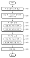
도 4는 본 발명의 일 실시예에 따른 기판 처리 방법을 보여주는 도면이다.
384 : 노즐 400 : 제어기
Claims (12)
- 기판 처리 방법에 있어서,
기판 상에 세정액을 분사하는 세정 단계;
세정이 완료된 기판 상에 린스액을 분사하는 린스 단계;
린스가 완료된 기판을 건조하는 건조 단계를 포함하되,
상기 린스 단계는,
상기 기판을 제 1 속도로 회전하는 제 1 린스 단계; 및
상기 기판을 상기 제 1 속도와 상이한 제 2 속도로 회전시키는 제 2 린스 단계를 포함하는 기판 처리 방법. - 제 1항에 있어서,
상기 제 2 속도는 상기 제 1 속도보다 작은 속도인 기판 처리 방법. - 제 2 항에 있어서,
상기 제 2 린스 단계는, 상기 린스액을 토출하는 린스액 노즐을 상기 기판 상부를 스캔 이동시키는 단계를 더 포함하는 기판 처리 방법. - 제 3 항에 있어서,
상기 린스액 노즐은 상기 기판의 중앙 영역에서 상기 기판의 가장자리 영역으로 스캔 이동하는 기판 처리 방법. - 제 3항에 있어서,
상기 제 1 린스 단계는, 상기 제 2 린스 단계 진입 전에 상기 기판의 회전 속도를 상기 제 1 속도에서 상기 제 2 속도로 바꾸는 기판 처리 방법. - 제 5항에 있어서,
상기 건조 단계는, 상기 기판 상으로 질소를 공급하는 단계를 더 포함하는 기판 처리 방법. - 제 1 항 내지 제 6 항 중 어느 한 항에 있어서,
상기 건조 단계는 유기용제를 공급하지 않고 이루어지는 기판 처리 방법. - 기판 처리 장치에 있어서,
기판이 처리되는 공간을 제공하는 하우징;
상기 하우징 내에 상기 기판을 지지 및 회전하는 스핀 헤드;
상기 기판 상으로 세정액을 공급하여 세정 공정을 수행하는 세정액 공급부재 및 린스액을 공급하여 린스 공정을 수행하는 린스액 공급부재를 갖는 노즐 유닛;
상기 스핀 헤드 및 상기 노즐 유닛을 제어하는 제어기를 포함하되,
상기 제어기는 상기 린스 공정을 수행할 때, 상기 기판을 제 1 속도로 회전시킨 후에 상기 기판을 상기 제 1 속도와 상이한 제 2 속도로 회전시키도록 상기 스핀 헤드를 제어하는 기판 처리 장치. - 제 8항에 있어서,
상기 제 2 속도는 상기 제 1 속도보다 작은 속도인 기판 처리 장치. - 제 9 항에 있어서,
상기 제어기는, 상기 기판을 상기 제 2 속도로 회전시킬 때, 상기 린스액 노즐을 상기 기판 위로 스캔 이동시키도록 상기 린스액 노즐을 제어하는 기판 처리 장치. - 제 10 항에 있어서,
상기 제어기는 상기 린스액 노즐을 상기 기판의 중앙 영역에서 상기 기판의 가장자리 영역으로 스캔 이동시키도록 상기 린스액 노즐을 제어하는 기판 처리 장치. - 제 8 항 내지 제 11 항 중 어느 한 항에 있어서,
상기 제어기는 상기 세정 공정 및 상기 린스 공정 후 상기 기판을 건조하는 건조 공정을 수행하도록 상기 스핀 헤드 및 상기 노즐 유닛을 제어하되, 상기 건조 공정은 유기용제의 공급없이 이루어지도록 상기 스핀 헤드 및 상기 노즐 유닛을 제어하는 기판 처리 장치.
Priority Applications (1)
| Application Number | Priority Date | Filing Date | Title |
|---|---|---|---|
| KR1020140194772A KR20160083422A (ko) | 2014-12-31 | 2014-12-31 | 기판 처리 장치, 그리고 기판 처리 장치를 이용한 기판 처리 방법 |
Applications Claiming Priority (1)
| Application Number | Priority Date | Filing Date | Title |
|---|---|---|---|
| KR1020140194772A KR20160083422A (ko) | 2014-12-31 | 2014-12-31 | 기판 처리 장치, 그리고 기판 처리 장치를 이용한 기판 처리 방법 |
Publications (1)
| Publication Number | Publication Date |
|---|---|
| KR20160083422A true KR20160083422A (ko) | 2016-07-12 |
Family
ID=56504971
Family Applications (1)
| Application Number | Title | Priority Date | Filing Date |
|---|---|---|---|
| KR1020140194772A KR20160083422A (ko) | 2014-12-31 | 2014-12-31 | 기판 처리 장치, 그리고 기판 처리 장치를 이용한 기판 처리 방법 |
Country Status (1)
| Country | Link |
|---|---|
| KR (1) | KR20160083422A (ko) |
Cited By (2)
| Publication number | Priority date | Publication date | Assignee | Title |
|---|---|---|---|---|
| KR20220011264A (ko) * | 2020-07-20 | 2022-01-28 | 세메스 주식회사 | 기판 처리 장치, 그리고 기판 처리 방법 |
| CN115295440A (zh) * | 2021-05-04 | 2022-11-04 | 细美事有限公司 | 基板处理装置及方法 |
-
2014
- 2014-12-31 KR KR1020140194772A patent/KR20160083422A/ko not_active Application Discontinuation
Cited By (2)
| Publication number | Priority date | Publication date | Assignee | Title |
|---|---|---|---|---|
| KR20220011264A (ko) * | 2020-07-20 | 2022-01-28 | 세메스 주식회사 | 기판 처리 장치, 그리고 기판 처리 방법 |
| CN115295440A (zh) * | 2021-05-04 | 2022-11-04 | 细美事有限公司 | 基板处理装置及方法 |
Similar Documents
| Publication | Publication Date | Title |
|---|---|---|
| KR101621482B1 (ko) | 기판 처리 장치 및 방법 | |
| CN106816399B (zh) | 基板处理装置及方法 | |
| KR101329319B1 (ko) | 노즐 및 이를 갖는 기판처리장치 | |
| KR20140029095A (ko) | 기판 처리 방법 | |
| KR101471540B1 (ko) | 기판처리방법 및 기판처리장치 | |
| KR20160083422A (ko) | 기판 처리 장치, 그리고 기판 처리 장치를 이용한 기판 처리 방법 | |
| CN107564837B (zh) | 用于处理基板的装置和方法 | |
| CN107591315B (zh) | 用于处理基板的装置和方法 | |
| KR101870666B1 (ko) | 기판 처리 장치 | |
| KR101842125B1 (ko) | 기판 처리 장치 및 방법 | |
| KR101757811B1 (ko) | 기판 세정 방법 | |
| KR102121239B1 (ko) | 기판처리장치 및 방법 | |
| KR101736853B1 (ko) | 기판 처리 장치 및 방법 | |
| KR102096944B1 (ko) | 기판처리장치 및 방법 | |
| KR20130015637A (ko) | 기판처리장치 | |
| KR20170046490A (ko) | 기판 처리 장치 및 방법 | |
| KR102193031B1 (ko) | 기판처리장치 및 방법 | |
| KR20150068761A (ko) | 기판처리장치 | |
| KR102284471B1 (ko) | 처리액 노즐 및 기판 처리 장치 | |
| KR20160134922A (ko) | 기판 처리 장치 및 방법 | |
| KR102505075B1 (ko) | 기판 처리 장치 및 방법 | |
| KR102347973B1 (ko) | 기판 처리 장치 및 기판 처리 방법 | |
| KR101994420B1 (ko) | 기판 처리 장치 및 방법 | |
| KR20130015611A (ko) | 기판 처리 장치 | |
| KR102497794B1 (ko) | 기판 처리 장치 및 용기 세정 방법 |
Legal Events
| Date | Code | Title | Description |
|---|---|---|---|
| PA0109 | Patent application |
Patent event code: PA01091R01D Comment text: Patent Application Patent event date: 20141231 |
|
| PG1501 | Laying open of application | ||
| PA0201 | Request for examination |
Patent event code: PA02012R01D Patent event date: 20191115 Comment text: Request for Examination of Application Patent event code: PA02011R01I Patent event date: 20141231 Comment text: Patent Application |
|
| E902 | Notification of reason for refusal | ||
| PE0902 | Notice of grounds for rejection |
Comment text: Notification of reason for refusal Patent event date: 20210621 Patent event code: PE09021S01D |
|
| E601 | Decision to refuse application | ||
| PE0601 | Decision on rejection of patent |
Patent event date: 20211022 Comment text: Decision to Refuse Application Patent event code: PE06012S01D Patent event date: 20210621 Comment text: Notification of reason for refusal Patent event code: PE06011S01I |