KR20160071422A - Electro-optical device, driving method of electro-optical device, and electronic apparatus - Google Patents
Electro-optical device, driving method of electro-optical device, and electronic apparatus Download PDFInfo
- Publication number
- KR20160071422A KR20160071422A KR1020167012361A KR20167012361A KR20160071422A KR 20160071422 A KR20160071422 A KR 20160071422A KR 1020167012361 A KR1020167012361 A KR 1020167012361A KR 20167012361 A KR20167012361 A KR 20167012361A KR 20160071422 A KR20160071422 A KR 20160071422A
- Authority
- KR
- South Korea
- Prior art keywords
- signal
- signal line
- lines
- pixel
- scanning
- Prior art date
Links
Images


Classifications
-
- G—PHYSICS
- G09—EDUCATION; CRYPTOGRAPHY; DISPLAY; ADVERTISING; SEALS
- G09G—ARRANGEMENTS OR CIRCUITS FOR CONTROL OF INDICATING DEVICES USING STATIC MEANS TO PRESENT VARIABLE INFORMATION
- G09G3/00—Control arrangements or circuits, of interest only in connection with visual indicators other than cathode-ray tubes
- G09G3/20—Control arrangements or circuits, of interest only in connection with visual indicators other than cathode-ray tubes for presentation of an assembly of a number of characters, e.g. a page, by composing the assembly by combination of individual elements arranged in a matrix no fixed position being assigned to or needed to be assigned to the individual characters or partial characters
- G09G3/34—Control arrangements or circuits, of interest only in connection with visual indicators other than cathode-ray tubes for presentation of an assembly of a number of characters, e.g. a page, by composing the assembly by combination of individual elements arranged in a matrix no fixed position being assigned to or needed to be assigned to the individual characters or partial characters by control of light from an independent source
- G09G3/36—Control arrangements or circuits, of interest only in connection with visual indicators other than cathode-ray tubes for presentation of an assembly of a number of characters, e.g. a page, by composing the assembly by combination of individual elements arranged in a matrix no fixed position being assigned to or needed to be assigned to the individual characters or partial characters by control of light from an independent source using liquid crystals
- G09G3/3611—Control of matrices with row and column drivers
- G09G3/3674—Details of drivers for scan electrodes
- G09G3/3677—Details of drivers for scan electrodes suitable for active matrices only
-
- G—PHYSICS
- G09—EDUCATION; CRYPTOGRAPHY; DISPLAY; ADVERTISING; SEALS
- G09G—ARRANGEMENTS OR CIRCUITS FOR CONTROL OF INDICATING DEVICES USING STATIC MEANS TO PRESENT VARIABLE INFORMATION
- G09G3/00—Control arrangements or circuits, of interest only in connection with visual indicators other than cathode-ray tubes
- G09G3/20—Control arrangements or circuits, of interest only in connection with visual indicators other than cathode-ray tubes for presentation of an assembly of a number of characters, e.g. a page, by composing the assembly by combination of individual elements arranged in a matrix no fixed position being assigned to or needed to be assigned to the individual characters or partial characters
- G09G3/34—Control arrangements or circuits, of interest only in connection with visual indicators other than cathode-ray tubes for presentation of an assembly of a number of characters, e.g. a page, by composing the assembly by combination of individual elements arranged in a matrix no fixed position being assigned to or needed to be assigned to the individual characters or partial characters by control of light from an independent source
- G09G3/36—Control arrangements or circuits, of interest only in connection with visual indicators other than cathode-ray tubes for presentation of an assembly of a number of characters, e.g. a page, by composing the assembly by combination of individual elements arranged in a matrix no fixed position being assigned to or needed to be assigned to the individual characters or partial characters by control of light from an independent source using liquid crystals
- G09G3/3611—Control of matrices with row and column drivers
- G09G3/3648—Control of matrices with row and column drivers using an active matrix
-
- G—PHYSICS
- G09—EDUCATION; CRYPTOGRAPHY; DISPLAY; ADVERTISING; SEALS
- G09G—ARRANGEMENTS OR CIRCUITS FOR CONTROL OF INDICATING DEVICES USING STATIC MEANS TO PRESENT VARIABLE INFORMATION
- G09G3/00—Control arrangements or circuits, of interest only in connection with visual indicators other than cathode-ray tubes
- G09G3/20—Control arrangements or circuits, of interest only in connection with visual indicators other than cathode-ray tubes for presentation of an assembly of a number of characters, e.g. a page, by composing the assembly by combination of individual elements arranged in a matrix no fixed position being assigned to or needed to be assigned to the individual characters or partial characters
- G09G3/34—Control arrangements or circuits, of interest only in connection with visual indicators other than cathode-ray tubes for presentation of an assembly of a number of characters, e.g. a page, by composing the assembly by combination of individual elements arranged in a matrix no fixed position being assigned to or needed to be assigned to the individual characters or partial characters by control of light from an independent source
- G09G3/36—Control arrangements or circuits, of interest only in connection with visual indicators other than cathode-ray tubes for presentation of an assembly of a number of characters, e.g. a page, by composing the assembly by combination of individual elements arranged in a matrix no fixed position being assigned to or needed to be assigned to the individual characters or partial characters by control of light from an independent source using liquid crystals
- G09G3/3611—Control of matrices with row and column drivers
- G09G3/3614—Control of polarity reversal in general
-
- G—PHYSICS
- G09—EDUCATION; CRYPTOGRAPHY; DISPLAY; ADVERTISING; SEALS
- G09G—ARRANGEMENTS OR CIRCUITS FOR CONTROL OF INDICATING DEVICES USING STATIC MEANS TO PRESENT VARIABLE INFORMATION
- G09G3/00—Control arrangements or circuits, of interest only in connection with visual indicators other than cathode-ray tubes
- G09G3/001—Control arrangements or circuits, of interest only in connection with visual indicators other than cathode-ray tubes using specific devices not provided for in groups G09G3/02 - G09G3/36, e.g. using an intermediate record carrier such as a film slide; Projection systems; Display of non-alphanumerical information, solely or in combination with alphanumerical information, e.g. digital display on projected diapositive as background
- G09G3/003—Control arrangements or circuits, of interest only in connection with visual indicators other than cathode-ray tubes using specific devices not provided for in groups G09G3/02 - G09G3/36, e.g. using an intermediate record carrier such as a film slide; Projection systems; Display of non-alphanumerical information, solely or in combination with alphanumerical information, e.g. digital display on projected diapositive as background to produce spatial visual effects
-
- G—PHYSICS
- G09—EDUCATION; CRYPTOGRAPHY; DISPLAY; ADVERTISING; SEALS
- G09G—ARRANGEMENTS OR CIRCUITS FOR CONTROL OF INDICATING DEVICES USING STATIC MEANS TO PRESENT VARIABLE INFORMATION
- G09G3/00—Control arrangements or circuits, of interest only in connection with visual indicators other than cathode-ray tubes
- G09G3/20—Control arrangements or circuits, of interest only in connection with visual indicators other than cathode-ray tubes for presentation of an assembly of a number of characters, e.g. a page, by composing the assembly by combination of individual elements arranged in a matrix no fixed position being assigned to or needed to be assigned to the individual characters or partial characters
- G09G3/2007—Display of intermediate tones
-
- G—PHYSICS
- G09—EDUCATION; CRYPTOGRAPHY; DISPLAY; ADVERTISING; SEALS
- G09G—ARRANGEMENTS OR CIRCUITS FOR CONTROL OF INDICATING DEVICES USING STATIC MEANS TO PRESENT VARIABLE INFORMATION
- G09G2300/00—Aspects of the constitution of display devices
- G09G2300/04—Structural and physical details of display devices
- G09G2300/0421—Structural details of the set of electrodes
- G09G2300/0426—Layout of electrodes and connections
-
- G—PHYSICS
- G09—EDUCATION; CRYPTOGRAPHY; DISPLAY; ADVERTISING; SEALS
- G09G—ARRANGEMENTS OR CIRCUITS FOR CONTROL OF INDICATING DEVICES USING STATIC MEANS TO PRESENT VARIABLE INFORMATION
- G09G2310/00—Command of the display device
- G09G2310/02—Addressing, scanning or driving the display screen or processing steps related thereto
- G09G2310/0243—Details of the generation of driving signals
- G09G2310/0251—Precharge or discharge of pixel before applying new pixel voltage
-
- G—PHYSICS
- G09—EDUCATION; CRYPTOGRAPHY; DISPLAY; ADVERTISING; SEALS
- G09G—ARRANGEMENTS OR CIRCUITS FOR CONTROL OF INDICATING DEVICES USING STATIC MEANS TO PRESENT VARIABLE INFORMATION
- G09G2310/00—Command of the display device
- G09G2310/02—Addressing, scanning or driving the display screen or processing steps related thereto
- G09G2310/0264—Details of driving circuits
- G09G2310/0297—Special arrangements with multiplexing or demultiplexing of display data in the drivers for data electrodes, in a pre-processing circuitry delivering display data to said drivers or in the matrix panel, e.g. multiplexing plural data signals to one D/A converter or demultiplexing the D/A converter output to multiple columns
-
- G—PHYSICS
- G09—EDUCATION; CRYPTOGRAPHY; DISPLAY; ADVERTISING; SEALS
- G09G—ARRANGEMENTS OR CIRCUITS FOR CONTROL OF INDICATING DEVICES USING STATIC MEANS TO PRESENT VARIABLE INFORMATION
- G09G2310/00—Command of the display device
- G09G2310/06—Details of flat display driving waveforms
- G09G2310/067—Special waveforms for scanning, where no circuit details of the gate driver are given
-
- G—PHYSICS
- G09—EDUCATION; CRYPTOGRAPHY; DISPLAY; ADVERTISING; SEALS
- G09G—ARRANGEMENTS OR CIRCUITS FOR CONTROL OF INDICATING DEVICES USING STATIC MEANS TO PRESENT VARIABLE INFORMATION
- G09G2320/00—Control of display operating conditions
- G09G2320/02—Improving the quality of display appearance
- G09G2320/0209—Crosstalk reduction, i.e. to reduce direct or indirect influences of signals directed to a certain pixel of the displayed image on other pixels of said image, inclusive of influences affecting pixels in different frames or fields or sub-images which constitute a same image, e.g. left and right images of a stereoscopic display
- G09G2320/0214—Crosstalk reduction, i.e. to reduce direct or indirect influences of signals directed to a certain pixel of the displayed image on other pixels of said image, inclusive of influences affecting pixels in different frames or fields or sub-images which constitute a same image, e.g. left and right images of a stereoscopic display with crosstalk due to leakage current of pixel switch in active matrix panels
-
- G—PHYSICS
- G09—EDUCATION; CRYPTOGRAPHY; DISPLAY; ADVERTISING; SEALS
- G09G—ARRANGEMENTS OR CIRCUITS FOR CONTROL OF INDICATING DEVICES USING STATIC MEANS TO PRESENT VARIABLE INFORMATION
- G09G2320/00—Control of display operating conditions
- G09G2320/02—Improving the quality of display appearance
- G09G2320/0233—Improving the luminance or brightness uniformity across the screen
-
- G—PHYSICS
- G09—EDUCATION; CRYPTOGRAPHY; DISPLAY; ADVERTISING; SEALS
- G09G—ARRANGEMENTS OR CIRCUITS FOR CONTROL OF INDICATING DEVICES USING STATIC MEANS TO PRESENT VARIABLE INFORMATION
- G09G2320/00—Control of display operating conditions
- G09G2320/02—Improving the quality of display appearance
- G09G2320/0257—Reduction of after-image effects
Abstract
전기 광학 장치는, 선택 신호(S1)가 출력될 때, 대응하는 제1 신호선이 선택되는 제어 회로를 포함한다. 선택 신호(S2)가 선택 신호(S1)의 출력 주기 동안에 출력되는 경우, 대응하는 제2 신호선이 선택된다. 제어 회로는 제1 및 제2 신호선의 부분적 선택 기간에서 중복 기간이 발생하도록 선택 신호를 출력한다. 마찬가지로, 제어 회로는 선택 신호(S2)에 대응하는 제2 신호선 및 선택 신호(S3)에 대응하는 제3 신호선의 부분적 선택 기간에서, 또는 선택 신호(S3)에 대응하는 제3 신호선 및 선택 신호(S4)에 대응하는 제4 신호선의 부분적 선택 기간에서 중복 기간이 발생하도록 선택 신호를 출력한다.The electro-optical device includes a control circuit in which a corresponding first signal line is selected when a selection signal (S1) is output. When the selection signal S2 is output during the output period of the selection signal S1, the corresponding second signal line is selected. The control circuit outputs a selection signal so that an overlap period occurs in the partial selection period of the first and second signal lines. Similarly, in the partial selection period of the second signal line corresponding to the selection signal S2 and the third signal line corresponding to the selection signal S3, or the third signal line corresponding to the selection signal S3 and the selection signal S4 in the partial selection period of the fourth signal line.
Description
본 발명은, 예를 들어 액정 장치 등의 전기 광학 장치, 전기 광학 장치의 구동 방법, 및 해당 전기 광학 장치로 구성되는, 예를 들어 액정 프로젝터 등의 전자 기기의 기술 분야에 관한 것이다.BACKGROUND OF THE
2K1K라고 불리는 고해상도의 디스플레이에 있어서는, 화소 간에 발생하는 횡전계의 영향이 크고, 화소 1개의 라인마다 화소 전극 전위의 극성을 반전시키는 H 라인 반전 구동 시스템을 채택할 수 없기 때문에, 각 프레임마다 화소 전극 전위의 극성을 반전시키는 프레임 반전 구동 시스템이 채택되어 있다. 일반적인 프레임 반전 구동 시스템에서는, 60Hz의 프레임 주파수가 사용되고 있지만, 2K1K라고 불리는 고해상도의 디스플레이에 있어서는 60Hz의 프레임 주파수를 사용하면, 플리커(flicker)의 영향이 커진다. 따라서, 2K1K라고 불리는 고해상도의 디스플레이에 있어서는, 프레임 주파수가 120Hz인 배속 구동이 채택되어 있다.In the high-resolution display called 2K1K, the influence of the transverse electric field generated between the pixels is large, and since the H line inversion driving system which reverses the polarity of the pixel electrode electric potential for each pixel line can not be adopted, A frame inversion driving system for inverting the polarity of the potential is adopted. In a general frame inversion driving system, a frame frequency of 60 Hz is used, but in a high-resolution display called 2K1K, the influence of a flicker becomes large when a frame frequency of 60 Hz is used. Therefore, in a high resolution display called 2K1K, double speed driving with a frame frequency of 120Hz is adopted.
그러나, 배속 구동을 채택한 경우에는, 각 신호선의 선택 기간이 짧아져서, 화소에 대한 표시 데이터 신호의 기입에 문제가 발생하고, 화질이 저하한다는 문제가 있다. 따라서, 종래는, 예를 들어 구동용 IC를 4개 또는 6개 사용하고, 수평 방향 및 수직 방향 양쪽으로 2개 또는 3개의 구동용 IC로 분담해서 이들 IC들을 구동함으로써, 선택 시간이 짧아지지 않도록 설정된다(예를 들어, 특허문헌 1, 특허문헌 2, 및 특허문헌 3을 참조한다).However, when double speed driving is adopted, there is a problem that the selection period of each signal line is shortened, a problem occurs in writing of the display data signal to the pixel, and image quality is lowered. Therefore, conventionally, for example, four or six driving ICs are used, and these ICs are driven by two or three driving ICs in both the horizontal direction and the vertical direction, so that the selection time is not shortened (See, for example,
그러나, 구동용 IC를 4개 또는 6개 사용하는 경우에는, 제조 비용이 상승한다는 문제가 있다. 또한, 구동용 IC를 4개 또는 6개 사용하는 경우에는, 하나의 화소 행당 2개의 신호선을 배선하는 것이 필요하게 되고, 화소의 구조가 복잡해진다. 구동용 IC를 증가시키지 않을 경우에는, 하나의 신호선의 선택 기간이 짧아져서, 화소에 대한 표시 데이터 신호의 기입에 지장이 발생하고, 화질이 저하한다는 문제가 있다.However, when four or six driving ICs are used, there is a problem that the manufacturing cost increases. Further, when four or six driving ICs are used, it is necessary to wire two signal lines per one pixel line, and the structure of the pixel becomes complicated. When the driving IC is not increased, the selection period of one signal line is shortened, and there arises a problem that writing of the display data signal to the pixel is hindered and the picture quality is lowered.
본 발명은, 화소 구조를 복잡하게 하지 않고, 제조 비용을 증가시키지 않으면서 화상의 저하를 방지하는 것이 가능한 전기 광학 장치, 전기 광학 장치의 구동 방법, 및 전기 광학 장치를 포함한 전자 기기를 제공하는 것을 목적으로 한다.It is an object of the present invention to provide an electro-optical device, a driving method of the electro-optical device, and an electronic apparatus including the electro-optical device capable of preventing image degradation without increasing the manufacturing cost without complicating the pixel structure The purpose.
본 발명의 양태에 따르면, 상기 목적을 해결하기 위해서는, 복수의 주사선; 복수의 신호선; 상기 복수의 주사선 및 상기 복수의 주사선의 교차에 각각 대응하도록 제공된 화소; 주사선에 주사 신호를 공급하는 주사선 구동부; 적어도 표시해야 할 계조에 대응하는 크기의 데이터 전압이 시분할 다중화된 화상 신호를 상기 화소에 상기 신호선을 통해 공급하는 신호선 구동부; 제어 신호에 따라, 상기 화상 신호를 공급하는 신호선을 선택하는 신호선 선택부; 및 상기 신호선 중 하나를 선택하는 중에, 다른 상기 신호선을 선택하고, 상기 신호선의 선택 기간의 일부에서 중복 기간이 발생하도록 상기 제어 신호를 출력하는 제어부를 포함하고, 여기서 상기 화소는, 화소 전극, 공통 전극, 상기 화소 전극과 상기 공통 전극과의 사이에 개재된 액정, 및 상기 화소 전극과 상기 신호선과의 사이에 제공되고, 상기 주사선을 통해 공급되는 주사 신호에 기초하여 온 상태 또는 오프 상태 중 어느 한쪽이 되도록 제어되는 스위칭 소자를 포함하는, 전기 광학 장치가 제공된다.According to an aspect of the present invention, in order to solve the above-described object, a plurality of scanning lines; A plurality of signal lines; A pixel provided so as to correspond to an intersection of the plurality of scanning lines and the plurality of scanning lines, respectively; A scan line driver for supplying scan signals to the scan lines; A signal line driver for supplying an image signal obtained by time-division multiplexing a data voltage having a magnitude corresponding to at least a gradation to be displayed to the pixel through the signal line; A signal line selection unit for selecting a signal line for supplying the image signal according to a control signal; And a control unit for selecting another one of the signal lines while selecting one of the signal lines and outputting the control signal so that an overlapping period occurs in a part of the selection period of the signal line, A liquid crystal interposed between the pixel electrode and the common electrode, and a liquid crystal provided between the pixel electrode and the signal line, the liquid crystal being provided between the pixel electrode and the common electrode, An electro-optical device including a switching element controlled to be turned on.
이 양태에 의하면, 주사선 구동부를 이용하여 주사선에 주사 신호가 공급되고, 적어도 표시해야 할 계조에 대응하는 크기의 데이터 전압이 시분할 다중화된 화상 신호가 신호선을 통해 화소에 공급된다. 이때, 화상 신호를 공급하는 신호선은, 제어 신호에 따라 신호선 선택부를 이용하여 선택되지만, 제어부에서는, 하나의 신호선의 선택 중에, 다른 신호선이 선택되고, 신호선의 선택 기간의 일부에서 중복 기간이 발생하도록 상기 제어 신호가 출력된다. 따라서, 고해상도로 인해, 화소당 데이터 전압의 기입 시간이 짧아지는 경우에도, 데이터 전압의 기입을 위한 신호선의 선택 기간의 일부에서 중복 기간이 발생하므로, 화소에 대하여 데이터 전압의 기입 시간을 충분히 확보할 수 있고, 화질을 향상시킨다.According to this aspect, a scanning signal is supplied to the scanning line by using the scanning line driver, and at least an image signal in which the data voltage of a size corresponding to the gradation to be displayed is time-division multiplexed is supplied to the pixel through the signal line. At this time, the signal line for supplying the image signal is selected by using the signal line selection unit in accordance with the control signal, but in the control unit, another signal line is selected during the selection of one signal line, and an overlap period is generated in a part of the selection period of the signal line The control signal is output. Therefore, even when the writing time of the data voltage per pixel is short due to the high resolution, an overlap period occurs in a part of the selection period of the signal line for writing the data voltage, so that the writing time of the data voltage to the pixel is sufficiently secured And improve picture quality.
상기 전기 광학 장치에 있어서, 상기 제어부는, 시분할 다중화된 상기 화상 신호의 개별 데이터 전압에 동기되는 타이밍보다도 빠른 타이밍에서, 상기 신호선을 선택하는 상기 제어 신호를 출력할 수 있다. 이 양태에 의하면, 화소에 대하여 데이터 전압의 기입 시간을 충분히 확보할 수 있고, 화질을 향상시킨다.In the electro-optical device, the control section can output the control signal for selecting the signal line at a timing earlier than the timing synchronized with the individual data voltage of the image signal that is time-division-multiplexed. According to this aspect, the writing time of the data voltage with respect to the pixel can be sufficiently secured, and the image quality is improved.
상기 전기 광학 장치에 있어서, 상기 신호선 구동부는, 적어도, 상기 화소에 상기 데이터 전압을 공급하기 전의 프리차지 기간에 있어서, 상기 신호선에 프리차지 전압을 공급할 수 있고, 상기 제어부는, 상기 프리차지 기간에 있어서, 모든 상기 신호선을 선택하는 상기 제어 신호를 출력할 수 있다. 이 양태에 의하면, 화소로부터의 누설에 의한 영향을 방지함으로써, 불균일한 휘도, 또는 수직 크로스 토크를 방지할 수 있다.In the electro-optical device, the signal line driver may supply a pre-charge voltage to the signal line at least in a pre-charge period before supplying the data voltage to the pixel, So that the control signal for selecting all the signal lines can be outputted. According to this aspect, it is possible to prevent uneven brightness or vertical crosstalk by preventing the influence of leakage from the pixel.
상기 전기 광학 장치에 있어서, 상기 주사선 구동부는, 상기 프리차지 기간에, 상기 스위칭 소자를 온 상태로 하는 상기 주사 신호를 상기 주사선에 공급할 수 있다. 이 양태에 의하면, 화소로부터의 누설에 의한 영향을 방지함으로써, 불균일한 휘도, 또는 수직 크로스 토크를 방지할 수 있다.In the electro-optical device, the scanning line driver may supply the scanning signal to turn on the switching element in the pre-charging period. According to this aspect, it is possible to prevent uneven brightness or vertical crosstalk by preventing the influence of leakage from the pixel.
상기 전기 광학 장치에 있어서, 상기 신호선 구동부는, 상기 프리차지 기간과, 하나의 수평 주사 기간에 최초에 선택되는 상기 신호선의 선택 기간의 전체 기간에 있어서, 최초에 선택되는 상기 신호선을 선택하는 상기 제어 신호를 출력할 수 있다. 이 양태에 의하면, 신호선에 대한 프리차지 전압의 기입으로 인해 화소로부터의 누설에 의한 영향을 방지함으로써 불균일한 휘도, 또는 수직 크로스 토크를 방지하여, 화소에 대하여 데이터 전압의 기입 시간을 충분히 확보할 수 있고, 화질을 향상시킨다.In the electro-optical device, the signal line driver may control the signal line driver to select the signal line initially selected in the pre-charge period and the entire period of the selection period of the signal line to be initially selected in one horizontal scanning period A signal can be output. According to this aspect, it is possible to prevent uneven luminance or vertical crosstalk by preventing the influence of leakage from the pixel due to the writing of the precharge voltage to the signal line, thereby sufficiently securing the writing time of the data voltage to the pixel And improves picture quality.
상기 전기 광학 장치에 있어서, 상기 신호선 구동부는, 상기 제어 신호를 이용하여 상기 신호선의 선택 순서를 자주 변경할 수 있다. 이 양태에 의하면, 중복 기간 동안에 선택되는 신호선 중에서, 미리 선택되는 신호선에 대응하는 화소의 데이터 전압을 이용하여, 후에 선택되는 신호선에 대응하는 화소에 대한 영향을 균일화할 수 있다.In the electro-optical device, the signal line driver may frequently change the selection order of the signal lines using the control signal. According to this aspect, among the signal lines selected during the overlap period, the data voltage of the pixel corresponding to the previously selected signal line can be used to equalize the influence on the pixel corresponding to the signal line to be subsequently selected.
본 발명의 다른 양태에 의하면, 전기 광학 장치의 제어 방법이 제공되는데, 이 전기 광학 장치는 복수의 주사선, 복수의 신호선, 상기 복수의 주사선 및 상기 복수의 주사선의 교차에 각각 대응하도록 제공된 화소를 포함하며, 여기서 상기 화소는, 화소 전극, 공통 전극, 상기 화소 전극과 상기 공통 전극에 개재된 액정, 및 상기 화소 전극과 상기 신호선과의 사이에 제공되고, 상기 주사선을 통해 공급되는 주사 신호에 기초하여 온 상태 또는 오프 상태 중 어느 한쪽이 되도록 제어되는 스위칭 소자를 포함하며, 상기 방법은 상기 주사선에 상기 주사 신호를 공급하는 단계; 적어도 표시해야 할 계조에 대응하는 크기의 데이터 전압이 시분할 다중화된 화상 신호를 상기 화소에 상기 신호선을 통해 공급하는 단계; 제어 신호에 따라, 상기 화상 신호를 공급하는 전기 신호선을 선택하는 단계; 상기 신호선 중 하나를 선택하는 중에, 다른 신호선을 선택하는 단계; 및 상기 신호선의 선택 기간의 일부에서 중복 기간이 발생하도록 상기 제어 신호를 출력하는 단계를 포함한다.According to another aspect of the present invention, there is provided a control method of an electro-optical device, which includes a plurality of scanning lines, a plurality of signal lines, pixels provided so as to correspond to the intersections of the plurality of scanning lines and the plurality of scanning lines, respectively Wherein the pixel includes a pixel electrode, a common electrode, a liquid crystal interposed between the pixel electrode and the common electrode, and a liquid crystal provided between the pixel electrode and the signal line, based on a scanning signal supplied through the scanning line A switching element controlled to be either in an on state or an off state, the method comprising: supplying the scanning signal to the scanning line; Supplying an image signal in which a data voltage of a size corresponding to at least a gradation to be displayed is time-division-multiplexed to the pixel through the signal line; Selecting an electric signal line for supplying the image signal in accordance with a control signal; Selecting another signal line while selecting one of the signal lines; And outputting the control signal such that an overlapping period occurs in a part of the selection period of the signal line.
본 발명의 또 다른 양태에 의하면, 상기 본 발명의 양태에 따른 전기 광학 장치를 포함하는 전자 기기가 제공된다. 그러한 전자 기기는, 고해상도로 인해, 화소당 데이터 전압의 기입 시간이 짧아지는 경우에도, 데이터 전압의 기입을 위한 신호선의 선택 기간의 일부에서 중복 기간이 발생하므로, 액정 디스플레이 등의 표시 장치에 있어서, 화소에 대하여 데이터 전압의 기입 시간을 충분히 확보할 수 있고, 화질을 향상시킬 수 있다.According to still another aspect of the present invention, there is provided an electronic apparatus including the electro-optical device according to the aspect of the present invention. In such a display device of a liquid crystal display or the like, such an electronic device generates a redundant period in a part of the selection period of the signal line for writing the data voltage even when the writing time of the data voltage per pixel is short due to the high resolution, The writing time of the data voltage with respect to the pixel can be sufficiently secured, and the image quality can be improved.
도 1은 본 발명의 제1 실시 형태에 관한 전기 광학 장치의 설명도이다.
도 2는 상기 실시 형태에 관한 전기 광학 장치의 구성을 도시하는 블록도이다.
도 3은 화소의 구성을 도시하는 회로도이다.
도 4는 상기 실시 형태에 관한 전기 광학 장치의 동작을 나타내는 타이밍 차트이다.
도 5는 본 발명의 제2 실시 형태에 관한 전기 광학 장치의 동작을 나타내는 타이밍 차트이다.
도 6은 본 발명의 제3 실시 형태에 관한 전기 광학 장치의 동작을 나타내는 타이밍 차트이다.
도 7은 변형예에 관한 전기 광학 장치의 동작을 나타내는 타이밍 차트이다.
도 8은 종래의 전기 광학 장치의 동작을 나타내는 타이밍 차트이다.
도 9는 전자 기기의 일례를 나타내는 설명도이다.
도 10은 전자 기기의 다른 예를 나타내는 설명도이다.
도 11은 전자 기기의 다른 예를 나타내는 설명도이다.1 is an explanatory diagram of an electro-optical device according to a first embodiment of the present invention.
2 is a block diagram showing the configuration of the electro-optical device according to the embodiment.
3 is a circuit diagram showing the configuration of a pixel.
4 is a timing chart showing the operation of the electro-optical device according to the embodiment.
5 is a timing chart showing the operation of the electro-optical device according to the second embodiment of the present invention.
6 is a timing chart showing the operation of the electro-optical device according to the third embodiment of the present invention.
7 is a timing chart showing the operation of the electro-optical device according to the modified example.
8 is a timing chart showing the operation of the conventional electro-optical device.
9 is an explanatory diagram showing an example of an electronic apparatus.
10 is an explanatory view showing another example of the electronic apparatus.
11 is an explanatory view showing another example of the electronic apparatus.
<제1 실시 형태>≪ First Embodiment >
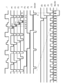
도 1은 전기 광학 장치(1)에 대한 신호 전송 시스템의 구성을 도시하는 도면이다. 도 1에 도시한 바와 같이, 전기 광학 장치(1)는, 전기 광학 패널(100), 구동용 집적 회로(200), 및 플렉시블 회로 기판(300)을 포함하고, 전기 광학 패널(100)은, 구동용 집적 회로(200)가 탑재된 플렉시블 회로 기판(300)에 접속되어 있다. 전기 광학 패널(100)은, 호스트 CPU로부터의 플렉시블 회로 기판(300), 및 구동용 집적 회로(200)를 통해 호스트 CPU(도시하지 않음)에 접속되어 있다. 여기서, 구동용 집적 회로(200)는, 플렉시블 회로 기판(300)을 통해 화상 신호, 및 구동 제어를 위한 각종 제어 신호를 수신하고, 플렉시블 회로 기판(300)을 통해 전기 광학 패널(100)을 구동하는 장치이다.Fig. 1 is a diagram showing a configuration of a signal transmission system for the electro-
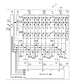
도 2는, 전기 광학 패널(100), 및 구동용 집적 회로(200)의 구성을 도시하는 블록도이다. 도 2에 도시한 바와 같이, 전기 광학 패널(100)은, 화소부(10), 주사선 구동부로서의 주사선 구동 회로(22), 및 신호선 선택부로서의 J개의 디멀티플렉서(57[1] 내지 57[J])를 포함하고 있다. 구동용 집적 회로(200)는, 신호선 구동부로서의 데이터선 구동 회로(30), 및 제어부로서의 제어 회로(40)를 포함하고 있다.2 is a block diagram showing the configuration of the electro-
화소부(10)는, 서로 교차하는 M개의 주사선(12)과 N개의 신호선(14)으로 형성되어 있다(M 및 N은 자연수). 복수의 화소 회로 PIX는, 각 주사선(12)과 각 신호선(14)의 교차에 대응해서 제공되어 있고, 수직 M행 × 수평 N열의 행렬로 배열되어 있다.The
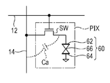
도 3은, 각 화소 회로 PIX의 회로도이다. 도 3에 도시한 바와 같이, 각 화소 회로 PIX는, 액정 소자(60), 및 TFT 등의 스위칭 소자 SW를 포함한다. 액정 소자(60)는, 서로 대향하는 화소 전극(62)과 공통 전극(64), 및 이들 전극 간의 액정(66)으로 구성되는 전기 광학 소자이다. 화소 전극(62)과 공통 전극(64)과의 사이의 인가 전압에 따라서 액정(66)의 투과율(표시 계조)이 변화한다. 또한, 액정 소자(60)에 병렬로 보조 용량을 접속한 구성도 채택될 수 있다. 스위칭 소자 SW는, 예를 들어 주사선(12)에 게이트가 접속된 N 채널형의 트랜지스터로 구성되고, 액정 소자(60)와 신호선(14)과의 사이에 제공되어 이들 간의 전기적인 접속(도통/절연)을 제어한다. 주사 신호 Y[m]가 선택 전위로 설정되면, 제m행 상의 각 화소 회로 PIX에 있어서의 스위칭 소자 SW가 동시에 온 상태로 천이한다.3 is a circuit diagram of each pixel circuit PIX. As shown in Fig. 3, each pixel circuit PIX includes a
화소 회로 PIX에 대응하는 주사선(12)이 선택되고, 화소 회로 PIX의 스위칭 소자 SW가 온 상태로 제어되었을 때, 신호선(14)으로부터 화소 회로 PIX의 액정 소자(60)에는, 화소 회로 PIX에 공급되는 화상 신호 D[n]에 따른 전압이 인가되고, 화소 회로 PIX의 액정(66)은, 화상 신호 D[n]에 따른 투과율을 갖도록 설정된다. 또한, 광원(도시하지 않음)은 온(점등) 상태로 되고, 광원으로부터 광이 출사되면, 해당 광은, 화소 회로 PIX에 포함되는 액정 소자(60)의 액정(66)을 투과하고, 관찰자측으로 진행한다. 즉, 액정 소자(60)에 화상 신호 D[n]에 따른 전압이 인가되고, 광원이 온 상태로 되면, 화소 회로 PIX에 대응하는 화소는, 화상 신호 D[n]에 따른 계조를 표시하게 된다.When the
스위칭 소자 SW가 오프 상태로 되면, 화소 회로 PIX의 액정 소자(60)에, 화상 신호 D[n]에 따른 전압이 인가된 후, 이상적으로는, 화상 신호 D[n]에 대응하는 인가 전압이 유지된다. 따라서, 이상적으로는, 각 화소는, 스위칭 소자 SW의 온 상태와 후속의 온 상태 사이의 기간에 있어서, 화상 신호 D[n]에 따른 계조를 표시한다.When the switching element SW is turned off, the voltage corresponding to the image signal D [n] is applied to the
도 3에 도시한 바와 같이, 신호선(14)과 화소 전극(62)과의 사이(또는, 신호선(14)과, 화소 전극(62)과 스위칭 소자 SW를 전기적으로 접속하는 배선과의 사이)에는, 용량 Ca가 기생한다. 그로 인해, 스위칭 소자 SW가 오프 상태인 사이에, 신호선(14)의 전위 변동이 용량 Ca를 통해 화소 전극(62)에 전파되고, 액정 소자(60)의 인가 전압이 변동하는 경우가 있다.(Or between the
또한, 공통 전극(64)에는, 공통 선(도시하지 않음)을 통해, 일정한 전압인 공통 전압 LCCOM이 공급된다. 공통 전압 LCCOM으로서는, 화상 신호 D[n]의 중심 전압을 0V로 설정했을 때 약 -0.5V의 전압이 사용된다. 이 전압 값은, 스위칭 소자 SW 등의 특성에 따라 결정된다.The
본 실시 형태에 의하면, 소위 번-인을 방지하기 위해서, 액정 소자(60)에 인가되는 전압의 극성을 소정 주기에서 반전하는 극성 반전 구동을 채택한다. 이 예에서는, 신호선(14)을 통해 화소 회로 PIX에 공급되는 화상 신호 D[n]의 레벨을, 화상 신호 D[n]의 중심 전압에 대하여 단위 기간마다 반전한다. 단위 기간은, 화소 회로 PIX를 구동하는 동작에 1 단위의 기간이다. 이 예에서는, 단위 기간은 수직 주사 기간으로 설정된다. 그러나, 단위 기간은 임의로 설정될 수 있고, 예를 들어, 수직 주사 기간의 자연수배일 수 있다. 본 실시 형태에 따르면, 화상 신호 D[n]이 화상 신호 D[n]의 중심 전압에 대하여 고전압이 될 경우를 정 극성으로 설정하고, 화상 신호 D[n]이 화상 신호 D[n]의 중심 전압에 대하여 저전압이 될 경우를 부 극성으로 설정한다.According to the present embodiment, in order to prevent the so-called burn-in, the polarity reversal driving which inverts the polarity of the voltage applied to the
도 2의 설명을 참조하면, 제어 회로(40)는, 외부의 장치(도시하지 않음)로부터 입력되는 수직 동기 신호 Vs, 수평 동기 신호 Hs, 도트 클럭(dot clock) 신호 DCLK 등의 외부 신호에 기초하여, 주사선 구동 회로(22)와 데이터선 구동 회로(30)을 동기 제어한다. 이 동기 제어 하에, 주사선 구동 회로(22)와 데이터선 구동 회로(30)는, 서로 협동해서 화소부(10)의 표시를 제어한다.2, the
주사선 구동 회로(22)는, 주사 신호 G[1] 내지 G[M]을 M개의 주사선(12)의 각각에 출력한다. 주사선 구동 회로(22)는, 제어 회로(40)로부터 수평 동기 신호 Hs의 출력에 따라, 각 주사선(12)에 대한 주사 신호 G[1] 내지 G[M]을 하나의 수평 주사 기간 H씩 순차적으로 액티브 레벨로 설정한다.The scanning
여기서, 제m행에 대응한 주사 신호 G[M]이 액티브 레벨이며, 해당 행에 대응한 주사선이 선택되고 있는 기간에는, 제m행의 N개의 화소 회로 PIX의 각 스위칭 소자 SW가 온 상태로 되고, 스위칭 소자 SW 각각을 통해 N개의 신호선(14) 각각이 제m행의 N개의 화소 회로 PIX의 각 화소 전극(62)에 접속된다.Here, in a period in which the scanning signal G [M] corresponding to the m-th row is at the active level and the scanning line corresponding to the row is selected, the respective switching elements SW of the N pixel circuits PIX in the m-th row are turned on And each of the N signal lines 14 is connected to each
화소부(10) 내의 N개의 신호선(14)은, 인접하는 4개의 신호선을 단위로서 설정함으로써 J개의 배선 블록 B[1] 내지 B[J]으로 구분되어 있다(J=N/4). 디멀티플렉서(57[1] 내지 57[J]) 각각은, J개의 배선 블록 B[1] 내지 B[J]에 대응하고 있다.The
디멀티플렉서(57[j])(j=1 내지 J)의 각각은, 4개의 스위치(58[1] 내지 58[4])로 구성되어 있다. 디멀티플렉서(57[j])(j=1 내지 J)의 각각에 있어서, 4개의 스위치(58[1] 내지 58[4])의 각각의 한쪽의 접점은 공통 접속되어 있다. 또한, 디멀티플렉서(57[j])(j=1 내지 J)의 각각의 4개의 스위치(58[1] 내지 58[4])의 한쪽의 접점의 공통 접속점 각각은, J개의 신호선(15)에 각각 접속되어 있다. J개의 신호선(15)은, 플렉시블 회로 기판(300)을 통해 구동용 집적 회로(200)의 데이터선 구동 회로(30)에 접속되어 있다. 또한, 디멀티플렉서(57[j])(j=1 내지 J)의 각각에 있어서, 4개의 스위치(58[1] 내지 58[4])의 각각의 다른 쪽의 각각의 접점은, 디멀티플렉서(57[j])에 대응한 배선 블록 B[j]을 구성하는 4개의 신호선(14)에 접속되어 있다.Each of the demultiplexers 57 [j] (j = 1 to J) is composed of four switches 58 [1] to 58 [4]. In each of the demultiplexers 57 [j] (j = 1 to J), the contacts of one of the four switches 58 [1] to 58 [4] are connected in common. Each of the common connection points of one of the four switches 58 [1] to 58 [4] of each of the demultiplexer 57 [j] (j = 1 to J) is connected to the J signal lines 15 Respectively. The J signal lines 15 are connected to the data line driving
디멀티플렉서(57[j])(j=1 내지 J) 각각의 4개의 스위치(58[1] 내지 58[4])의 온/오프는, 4개의 선택 신호 S1 내지 S4에 의해 각각 전환된다. 4개의 선택 신호 S1 내지 S4은, 플렉시블 회로 기판(300)을 통해 구동용 집적 회로(200)의 제어 회로(40)로부터 공급된다. 여기서, 하나의 선택 신호 S1이 액티브 레벨이고, 다른 3개의 선택 신호 S2 내지 S4이 비액티브 레벨일 경우에는, 디멀티플렉서(57[j])(j=1 내지 J)에 각각 속하는 J개의 스위치 중 스위치 58[1]만이 온 상태가 된다. 따라서, 디멀티플렉서(57[j])(j=1 내지 J)의 각각은, J개의 신호선(15) 상의 화상 신호 D[1] 내지 D[J]을 배선 블록 B[1] 내지 B[J] 각각의 제1 신호선(14)에 출력한다. 이하, 마찬가지로, J개의 신호선(15) 상의 화상 신호 D[1] 내지 D[J]가 배선 블록 B[1] 내지 B[J] 각각의 제2, 제3, 및 제4 신호선(14)에 각각 출력된다.The on / off of the four switches 58 [1] to 58 [4] of the demultiplexer 57 [j] (j = 1 to J) is switched by the four selection signals S1 to S4, respectively. The four selection signals S1 to S4 are supplied from the
제어 회로(40)는, 프레임 메모리를 갖고 있고, 화소부(10)의 해상도에 해당하는 M×N 비트의 메모리 공간을 적어도 포함하고 있고, 외부의 장치로부터 입력되는 표시 데이터를 프레임 단위로 저장 및 유지한다. 여기서, 화소부(10)의 계조를 규정하는 표시 데이터는, 일례로서, 6비트로 구성되는 64 계조의 데이터이다. 프레임 메모리로부터 판독된 표시 데이터는, 6비트의 버스를 통해 표시 데이터로서 데이터선 구동 회로(30)에 시리얼적으로 전송된다. 또한, 표시 데이터에는, 후술하는 프리차지 신호도 포함되어 있다.The
또한, 제어 회로(40)는, 적어도 1개의 라인의 라인 메모리를 포함하는 구성을 가질 수도 있다. 이 경우, 상기 라인 메모리에 있어서, 1개의 라인의 표시 데이터를 축적함으로써 표시 데이터를 각 화소에 전송한다.In addition, the
데이터선 구동 회로(30)는, 주사선 구동 회로(22)과 협동하여, 데이터의 기입 대상인 화소 행마다 공급해야 할 데이터를 신호선(14)에 출력한다. 데이터선 구동 회로(30)는, 제어 회로(40)로부터 출력되는 선택 신호 S1 내지 S4에 기초하여 래치 신호를 생성하고, 시리얼 데이터로서 공급된 N개의 6비트의 표시 데이터 신호를 순차 래치한다. 표시 데이터 신호는, 시계열적인 데이터로서 4개의 화소의 그룹으로 만들어진다. 또한, 데이터선 구동 회로(30)에는, D/A(digital to analog) 변환 회로가 제공되어 있고, 디지털 데이터 그룹에 대해 D/A 변환을 행하고, 아날로그 데이터로서의 전압을 생성한다. 이에 의해, 프리차지 신호는 소정의 프리차지 전압 Vpre으로 변환되고, 4개의 화소 단위로 시계열 신호인 표시 데이터 신호도 소정의 데이터 전압으로 변환된다. 또한, 프리차지 전압과 4개의 화소의 데이터 전압과의 세트는, 이러한 순서로 각각의 신호선(15)에 공급된다.The data line driving
디멀티플렉서(57[j])(j=1 내지 J)의 각각의 스위치(58[1] 내지 58[4])의 전기적 접속은, 제어 회로(40)로부터 출력되는 선택 신호 S1 내지 S4에 의해 제어되고, 스위치들은 소정의 타이밍에서 온 상태로 된다. 이에 의해, 1H에 있어서, 각 신호선(15)에 공급된 프리차지 전압과 4개의 화소의 데이터 전압과의 세트는, 스위치(58[1] 내지 58[4])를 사용하여 시계열적으로 신호선(14)에 출력된다.The electrical connections of the switches 58 [1] to 58 [4] of the demultiplexer 57 [j] (j = 1 to J) are controlled by the selection signals S1 to S4 output from the
이상은 전기 광학 장치(1)의 구성이다.The above is the configuration of the electro-
도 4는 구동용 집적 회로(200)의 타이밍 차트를 나타낸다. 외부의 장치로부터 제어 회로(40)에 수평 동기 신호 Hs가 입력되면, 제어 회로(40)는 수평 동기 신호 Hs에 동기시켜서 주사선 구동 회로(22)를 구동한다. 주사선 구동 회로(22)는, 1개의 프레임(1F) 주기의 Y 전송 개시 펄스 DY에 대응하는 신호에 대해, Y 클럭 신호 CLY에 따라 순차 시프트를 행함으로써 주사 신호 G[1], G[2], ..., G[n]을 생성한다. 주사 신호 G[1], G[2], ..., G[n]은 각각의 수평 주사 기간(1H)에 있어서 순차 액티브가 된다. 데이터선 구동 회로(30)는, 수평 주사 주기의 X 전송 개시 펄스 DX(도시하지 않음)과 X 클럭 신호 CLX(도시하지 않음)에 기초하여, 샘플링 펄스 SP1, SP2, ..., SPz(도시하지 않음)를 생성한다. 또한, 데이터선 구동 회로(30)는, 화상 신호 VID1 내지 VIDj(도시하지 않음)에 대해 샘플링 펄스 SP1, SP2, ..., SPz(도시하지 않음)를 사용해서 샘플링을 행함으로써 화상 신호 D[1] 내지 D[j]를 생성한다.Fig. 4 shows a timing chart of the driving
제어 회로(40)는, 수평 동기 신호 Hs에 동기시켜서 선택 신호 S1 내지 S4를 데이터선 구동 회로(30)와 디멀티플렉서(57[j])(j=1 내지 J)의 4개의 스위치(58[1] 내지 58[4])에 출력한다. 데이터선 구동 회로(30)는, 출력 단자 d1 내지 dj로부터 신호선(15)에 화상 신호 D[1] 내지 D[j]을 출력한다. 디멀티플렉서(57[j])(j=1 내지 J)의 4개의 스위치(58[1] 내지 58[4])는, 선택 신호 S1 내지 S4에 기초하여 온/오프 상태로 되고, 프리차지 신호를 포함하는 화상 신호 D[1] 내지 D[j]는 신호선(14)에 각각 출력된다.The
제어 회로(40)는, 주사 신호 G[1]가 액티브가 되는 타이밍 t0로부터 소정 시간 후의 타이밍 t1에 있어서, 선택 신호 S1 내지 S4를 동시에 액티브로 하고, 기간 T0에 걸쳐 선택 신호 S1 내지 S4의 액티브 상태를 유지한다. 이때, 화상 신호 D[1] 내지 D[j]는 프리차지 전압 Vpre에 설정되므로, 신호선(14) 및 화소에는 프리차지 전압 Vpre가 기입되게 된다.The
제어 회로(40)는, 타이밍 t2에서 선택 신호 S1 내지 S4을 비액티브로 한 후, 소정 시간 후의 타이밍 t3에 있어서, 선택 신호 S1을 액티브로 한다. 종래는, 도 8 에 도시한 바와 같이, 타이밍 t3보다도 늦은 타이밍 t4에서 선택 신호 S1을 액티브로 하지만, 본 실시 형태에 따르면, 타이밍 t4보다도 빠른 타이밍 t3에서 선택 신호 S1을 액티브로 한다. 그 결과, 선택 신호 S1이 액티브가 되는 기간은, 도 8에 나타내는 종래의 기간 T10보다도 길고, 도 4에 도시한 바와 같이 기간 T1이 된다.The
마찬가지로, 제어 회로(40)는, 타이밍 t5에서 선택 신호 S1을 비액티브로 하지만, 타이밍 t5보다 소정 시간 빠른 타이밍 t4에서 선택 신호 S2를 액티브로 한다. 종래는, 도 8 에 도시한 바와 같이, 타이밍 t4보다도 늦은 타이밍 t5에서 선택 신호 S2를 액티브로 하지만, 본 실시 형태에 따르면, 타이밍 t5보다도 빠른 타이밍 t4에서 선택 신호 S2를 액티브로 한다. 그 결과, 선택 신호 S2가 액티브가 되는 기간은, 도 8에 나타내는 종래의 기간 T11보다도 길고, 이 기간은 도 4에 도시한 바와 같이 기간 T3이 된다. 또한, 선택 신호 S1 및 선택 신호 S2을 이렇게 제어하기 때문에, 선택 신호 S1과 선택 신호 S2의 양쪽이 액티브가 되는 중복 기간 T2이 발생하게 된다.Likewise, the
이하, 마찬가지로, 제어 회로(40)는, 타이밍 t5에서 선택 신호 S3을 액티브로 하기 때문에, 선택 신호 S3이 액티브가 되는 기간은, 도 8에 나타내는 종래의 기간 T12보다도 길고, 이 기간은 도 4에 도시한 바와 같이 기간 T5이 된다. 그 결과, 선택 신호 S2과 선택 신호 S3의 양쪽이 액티브가 되는 중복 기간 T4이 발생하게 된다. 또한, 제어 회로(40)는, 타이밍 t6에서 선택 신호 S4를 액티브로 하기 때문에, 선택 신호 S4가 액티브가 되는 기간은, 도 8에 도시하는 종래의 기간 T13보다도 길고, 이 기간은 도 4에 도시한 바와 같이 기간 T7이 된다. 그 결과, 선택 신호 S3과 선택 신호 S4의 양쪽이 액티브가 되는 중복 기간 T6이 발생하게 된다.In the same manner, since the
이상과 같이, 본 실시 형태에 따르면, 신호선(14)을 선택하는 기간을 종래보다도 길게 하면서, 복수의 신호선(14)을 동시에 선택하는 중복 기간을 제공하도록 선택 신호를 구동하므로, 전기 광학 패널(100)의 해상도를 높게 설정한 경우라도, 데이터선 구동 회로를 증설하지 않고, 화소에 대한 화상 신호의 인가 시간을 충분히 확보할 수 있다. 그 결과, 전기 광학 패널(100)의 화질을 향상시킬 수 있다. 특히, 전기 광학 패널(100)에 있어서 3차원 표시(입체 표시)을 행하는 경우에는, 하나의 신호선(14)에 대응하는 화소에의 화소 전압의 인가 시간이 짧아지지만, 본 실시 형태를 적용함으로써 고화질의 3차원 표시를 행할 수 있다.As described above, according to the present embodiment, since the selection signal is driven so as to provide the overlapping period for simultaneously selecting the plurality of
본 실시 형태에 따르면, 상기 중복 기간에 있어서는, 각각의 배선 블록 B[1] 내지 B[J]에서 2개의 신호선(14)이 동시에 선택되면, 시간적으로 후에 선택된 신호선(14)에 대응하는 화소는, 시간적으로 먼저 선택된 신호선(14)에 대응하는 화소에 기입된 화소 전압에 의해 영향을 받게 된다. 그러나, 예를 들어, 시간적으로 먼저 선택된 신호선(14)에 대응하는 화소에는 가장 휘도가 낮은 화소 전압이 인가되고, 시간적으로 후에 선택된 신호선(14)에 대응하는 화소에는 가장 휘도가 높은 화소 전압이 인가되는 경우와 같이, 콘트라스트가 높은 경우에는, 육안으로는 상기 영향을 인식하기 어렵다. 또한, 모든 화소에 중간 휘도의 화소 전압이 인가되는 경우에는, 모두 화소에 동일한 화소 전압이 인가되므로, 상기 영향을 받지 않는다. 오히려, 모두 화소에 대한 화소 전압의 인가 시간이 길어지기 때문에, 화질이 향상된다.According to the present embodiment, in the overlap period, when two
<제2 실시 형태>≪ Second Embodiment >
제1 실시 형태에서는, 프리차지 신호를 인가하는 타이밍 t1보다도 조금 앞선 타이밍 t0에서, 주사 신호 G[1], G[2], ..., G[n]을 액티브로 하는 예에 대해서 설명했다. 그러나, 본 실시 형태에 따르면, 도 5에 도시한 바와 같이, 프리차지 신호의 인가 시에는, 주사 신호 G[1], G[2], ..., G[n]를 비액티브로 하면서, 최초에 선택된 선택 신호를 액티브로 하는 타이밍 t3보다도 조금 앞선 타이밍 t0'에서, 주사 신호 G[1], G[2], ..., G[n]을 액티브로 한다.In the first embodiment, an example has been described in which the scanning signals G [1], G [2], ..., G [n] are made active at a timing t0 slightly before the timing t1 for applying the precharge signal . However, according to the present embodiment, as shown in Fig. 5, the scan signals G [1], G [2], ..., G [n] The scanning signals G [1], G [2], ..., G [n] are made active at a timing t0 ', which is slightly before the timing t3 at which the selected selection signal is made active.
프리차지 신호의 인가는, 오프 상태로 되어 있는 화소 트랜지스터로부터 신호선(14)에의 누설의 영향에 의한 표시 불균일을 억제하기 위해서 행해지고, 본 실시 형태에서와 같이, 프리차지 신호의 인가 시에 있어서 주사 신호 G[1], G[2], ..., G[n]을 오프 상태로 해도, 화소 트랜지스터의 누설을 억제할 수 있다.The application of the precharge signal is performed in order to suppress display unevenness due to the influence of leakage from the pixel transistor which is in the off state to the
본 실시 형태에 있어서도, 타이밍 t0'에서 주사 신호 G[1], G[2], ..., G[n]를 액티브로 한 후, 선택 신호 S1, S2, S3, 및 S4를 액티브로 하는 기간을 종래에 비해 길게 설정하고, 복수의 신호선(14)을 동시에 선택하는 중복 기간을 제공하도록 선택 신호를 구동하므로, 전기 광학 패널(100)의 해상도를 높게 설정한 경우에도, 데이터선 구동 회로를 증설하지 않고, 화소에 대한 화소 전압의 인가 시간을 충분히 확보할 수 있고, 그 결과, 전기 광학 패널(100)의 화질을 향상시킬 수 있다.In this embodiment also, after the scanning signals G [1], G [2], ..., G [n] are made active at the timing t0 ', the selection signals S1, S2, S3, and S4 are made active Since the selection signal is driven so as to provide an overlap period in which the plurality of
<제3 실시 형태>≪ Third Embodiment >
제1 실시 형태에서는, 프리차지 신호를 인가하기 위해서 타이밍 t1에서 선택 신호 S1, S2, S3, 및 S4를 액티브로 하고, 그 후, 일단, 선택 신호 S1을 비액티브로 하고 난 다음, 타이밍 t3에서 화상 신호를 인가하기 위해서 선택 신호 S1을 액티브로 하는 예에 대해서 설명했다. 본 실시 형태에 따르면, 도 6 에 도시한 바와 같이, 프리차지 신호를 인가하기 위해서 타이밍 t1에서 선택 신호 S1, S2, S3, 및 S4를 액티브로 하고, 이후 선택 신호 S1의 액티브 상태를 그대로 계속하고, 그 다음 타이밍 t5에서 선택 신호 S1을 비액티브로 한다.In the first embodiment, in order to apply the precharge signal, the selection signals S1, S2, S3, and S4 are made active at the timing t1 and then the selection signal S1 is made inactive once, An example has been described in which the selection signal S1 is made active in order to apply an image signal. According to the present embodiment, as shown in Fig. 6, in order to apply the precharge signal, the selection signals S1, S2, S3, and S4 are made active at the timing t1 and then the active state of the selection signal S1 is maintained , And makes the selection signal S1 inactive at the next timing t5.
본 실시 형태에 따르면, 프리차지 신호의 인가 시간의 개시부터, 최초에 선택되는 선택 신호 S1의 선택의 종료까지, 선택 신호 S1의 액티브 상태가 계속되므로, 선택 신호 S1이 액티브가 되는 기간 T1'은, 제1 실시 형태에서보다도 길어진다. 그 결과, 프리차지 신호를 확실하게 인가하면서, 화소에 대한 화소 전압의 인가 시간을 보다 충분하게 확보할 수 있고, 전기 광학 패널(100)의 화질을 향상시킬 수 있다.According to the present embodiment, since the active state of the selection signal S1 continues from the start of the application time of the precharge signal until the end of the selection of the first selection signal S1 selected, the period T1 'during which the selection signal S1 becomes active , Which is longer than in the first embodiment. As a result, it is possible to sufficiently secure the application time of the pixel voltage to the pixel while reliably applying the pre-charge signal, and the image quality of the electro-
<변형예><Modifications>
본 발명은, 상기 각 실시 형태에 한정되는 것이 아니라, 예를 들어 이하에 설명하는 각종 변형을 수행할 수 있다. 또한, 물론, 각 실시 형태 및 각 변형예를 적절히 조합할 수 있다.The present invention is not limited to the above-described embodiments, and various modifications described below can be performed, for example. Needless to say, each embodiment and each variation can be suitably combined.
(1) 상기 각 실시 형태에 있어서는, 선택 신호 S1을 최초에 액티브로 하고, 그 후, 선택 신호 S2, S3, 및 S4를 이 순서로 액티브로 하는 예에 대해서 설명했지만, 본 발명은 이러한 예에 한정되는 것은 아니다. 예를 들어, 도 7에 도시한 바와 같이, 선택 신호 S4을 최초로 액티브로 하고, 그 후, 선택 신호 S1, S2, 및 S3을 이 순서로 액티브로 할 수 있다. 이 경우에는, 선택 신호 S4와 선택 신호 S1의 중복 기간이 T2로 설정되고, 선택 신호 S1과 선택 신호 S2의 중복 기간이 T4로 설정되고, 그리고 선택 신호 S2과 선택 신호 S3의 중복 기간이 T6으로 설정된다. 이와 같은 경우에도, 신호선(14)을 선택하는 기간을 종래보다도 길게 하면서, 복수의 신호선(14)을 동시에 선택하는 중복 기간이 제공되도록 선택 신호를 구동할 수 있다. 또한, 선택 신호를 액티브로 하는 순서는 임의의 순서일 수 있다.(1) In each of the above-described embodiments, an example has been described in which the selection signal S1 is initially made active, and thereafter the selection signals S2, S3, and S4 are made active in this order. But is not limited thereto. For example, as shown in Fig. 7, the selection signal S4 may be made active first, and then the selection signals S1, S2, and S3 may be made active in this order. In this case, the overlap period of the selection signal S4 and the selection signal S1 is set to T2, the overlap period of the selection signal S1 and the selection signal S2 is set to T4, and the overlap period of the selection signal S2 and the selection signal S3 is set to T6 Respectively. Even in such a case, the selection signal can be driven so that the period for selecting the
또한, 선택 신호를 액티브로 하는 순서를 수평 주사 기간마다 교체하거나, 수직 주사 기간마다 교체하는 구성을 채택할 수 있다. 또한, 수평 주사 기간마다 순서를 교체하면서, 수직 주사 기간마다 선택 신호를 액티브로 하는 순서도 교체하는 조합을 채택할 수 있다. 선택 신호를 액티브로 하는 순서의 교체는, 제1 수평 주사 기간에는 선택 신호 S1, S2, S3, 및 S4의 순서일 수 있고, 제2 수평 주사 기간에는 선택 신호 S2, S3, S4, 및 S1의 순서일 수 있고, 제3 수평 주사 기간에는 선택 신호 S3, S4, S1, 및 S2의 순서일 수 있고, 제4 수평 주사 기간에는 선택 신호 S4, S1, S2, 및 S3의 순서일 수 있고, 제5 수평 주사 기간 또는 그 이후에는 이들을 반복할 수 있다.Furthermore, a configuration in which the order of activating the selection signal is changed for each horizontal scanning period or is changed every vertical scanning period can be adopted. It is also possible to employ a combination in which the order of changing the selection signal for each vertical scanning period is changed while changing the order for each horizontal scanning period. In the second horizontal scanning period, the selection signals S2, S3, S4, and S1 may be switched in the order of selection signals S1, S2, S3, and S4 in the first horizontal scanning period, S1, and S2 in the third horizontal scanning period, and in the order of the selection signals S4, S1, S2, and S3 in the fourth horizontal scanning period, These can be repeated for 5 horizontal scanning periods or thereafter.
(2) N개의 신호선(14)이, 인접하는 4개의 신호선을 하나의 단위로 설정함으로써 J개의 배선 블록 B[1] 내지 B[J]으로 구분된 예에 대해서 설명하고 있지만, 신호선의 블록은 인접하는 4개의 신호선이 아닐 수 있고, 2개의 선, 3개의 선, 5개으 선, 6개의 선, 7개의 선, 8개의 선, ..., 및 n개의 선(n은 자연수)일 수 있다.(2) An example in which N signal lines 14 are divided into J wiring blocks B [1] to B [J] by setting four adjacent signal lines as one unit has been described, May not be four adjacent signal lines and may be two lines, three lines, five lines, six lines, seven lines, eight lines, ..., and n lines (n is a natural number) .
(3) 상기 실시 형태에 있어서는, 전기 광학 재료의 일례로서 액정을 채택했지만, 그 액정 이외의 전기 광학 재료를 사용한 전기 광학 장치에도 본 발명은 적용될 수 있다. 전기 광학 재료로서는, 전기 신호(전류 신호 또는 전압 신호)의 공급에 따라 투과율이나 휘도와 같은 광학적 특성이 변화하는 재료가 있다. 예를 들어, 유기 EL(electroLuminescent), 무기 EL, 또는 발광 중합체 등의 발광 소자를 사용한 표시 패널, 착색된 액체와 해당 액체에 분산된 백색의 입자를 포함하는 마이크로 캡슐을 전기 광학 재료로서 사용한 전기 영동 표시 패널, 극성이 서로 상이한 영역마다 상이한 색으로 도포되는 트위스트 볼을 전기 광학 재료로서 사용한 트위스트 볼 표시 패널, 흑색 토너를 전기 광학 재료로서 사용한 토너 표시 패널, 또는 헬륨이나 네온 등의 고압 가스를 전기 광학 재료로서 사용한 플라즈마 표시 패널 등 각종 전기 광학 장치에 대하여도 상기 실시 형태와 마찬가지로 본 발명을 적용할 수 있다.(3) In the above embodiment, liquid crystal is adopted as an example of the electro-optical material, but the present invention can be applied to an electro-optical device using an electro-optical material other than the liquid crystal. As the electro-optic material, there is a material whose optical characteristics such as transmittance and luminance change with supply of an electric signal (current signal or voltage signal). For example, a display panel using a light emitting element such as an organic EL (electro luminescent), an inorganic EL, or a light emitting polymer, a microcapsule containing a colored liquid and white particles dispersed in the liquid, A display panel, a twist ball display panel using a twist ball coated with a different color for different regions of different polarities as an electro-optical material, a toner display panel using a black toner as an electrooptic material, or a high-pressure gas such as helium or neon, The present invention can be applied to various electro-optical devices such as a plasma display panel used as a material in the same manner as in the above embodiments.
<응용예><Application example>
본 발명은, 각종 전자 기기에 이용될 수 있다. 도 9 내지 도 11은, 본 발명의 적용 대상으로서 전자 기기의 구체적인 형태를 예시하는 것이다.The present invention can be applied to various electronic apparatuses. Figs. 9 to 11 illustrate specific examples of the electronic device as an object to which the present invention is applied.
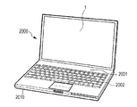
도 9는, 전기 광학 장치를 채택한 휴대용 퍼스널 컴퓨터의 사시도이다. 퍼스널 컴퓨터(2000)는, 각종 화상을 표시하는 전기 광학 장치(1)와, 전원 스위치(2001) 또는 키보드(2002)가 제공된 본체부(2010)를 포함한다.9 is a perspective view of a portable personal computer employing an electro-optical device. The
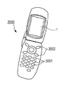
도 10은, 이동 전화기의 사시도이다. 이동 전화기(3000)는, 복수의 조작 버튼(3001), 스크롤 버튼(3002), 및 각종 화상을 표시하는 전기 광학 장치(1)를 포함한다. 스크롤 버튼(3002)을 조작할 때 전기 광학 장치(1) 상에 표시되는 화면이 스크롤된다. 본 발명은 이러한 이동 전화기에도 적용 가능하다.10 is a perspective view of a mobile phone. The
도 11은, 전기 광학 장치를 채택한 투사형 표시 장치(3판식 프로젝터)(4000)의 구성을 도시하는 개략도이다. 이 투사형 표시 장치(4000)는, 서로 상이한 R, G, 및 B의 표시 색에 각각 대응하는 3개의 전기 광학 장치(1)(1R, 1G, 및 1B)를 포함하고 있다. 조명 광학 시스템(4001)은, 조명 장치(광원)(4002)로부터의 출사광 가운데 적색 성분 r을 전기 광학 장치(1R)에 공급하고, 녹색 성분 g를 전기 광학 장치(1G)에 공급하며, 청색 성분 b를 전기 광학 장치(1B)에 공급한다. 각각의 전기 광학 장치(1)는, 조명 광학 시스템(4001)으로부터 공급되는 각각의 단색광을 표시 화상에 따라 변조하는 광 변조기(전구)로서 기능한다. 투사 광학 시스템(4003)은, 광을 합성함으로써 각각의 전기 광학 장치(1)로부터의 출사광을 투사면(4004)에 투사한다. 본 발명은 이러한 액정 프로젝터에도 적용 가능하다.11 is a schematic diagram showing the configuration of a projection display device (three-plate type projector) 4000 employing an electro-optical device. This
또한, 본 발명이 적용될 수 있는 전자 기기로서는, 도 1, 도 9, 및 도 10에 예시한 기기 이외에, 휴대 정보 단말기(Personal Digital Assistant(PDA)), 디지털 스틸 카메라, 텔레비전, 비디오 카메라, 카 내비게이션 장치, 차량용 표시기(인스트루먼트 패널), 전자 수첩, 전자 페이퍼, 계산기, 워드프로세서, 워크스테이션, 비디오폰, POS 단말기, 프린터, 스캐너, 복사기, 비디오 플레이어, 터치 패널을 포함한 기기 등을 들 수 있다.In addition to the devices illustrated in Figs. 1, 9, and 10, examples of electronic devices to which the present invention can be applied include portable digital assistants (PDAs), digital still cameras, televisions, video cameras, A device including a display device (instrument panel), an electronic notebook, an electronic paper, a calculator, a word processor, a workstation, a video phone, a POS terminal, a printer, a scanner, a copier, a video player and a touch panel.
1: 전기 광학 장치
10: 화소부
12: 주사선
14: 신호선
15: 신호선
22: 주사선 구동 회로
30: 데이터선 구동 회로
40: 제어 회로
57: 디멀티플렉서
58: 스위치
60: 액정 소자
62: 화소 전극
64: 공통 전극
66: 액정
100: 전기 광학 패널
200: 구동용 집적 회로1: electro-optical device
10:
12: Scanning line
14: Signal line
15: Signal line
22: scanning line driving circuit
30: Data line driving circuit
40: control circuit
57: Demultiplexer
58: Switch
60: liquid crystal element
62: pixel electrode
64: common electrode
66: liquid crystal
100: electro-optical panel
200: driving integrated circuit
Claims (12)
복수의 주사선;
복수의 신호선;
상기 복수의 주사선과 상기 복수의 신호선과의 교점에 각각 대응하도록 제공된 화소;
주사선에 주사 신호를 공급하는 주사선 구동부;
적어도 표시해야 할 계조에 대응하는 크기의 데이터 전압이 시분할 다중화된 화상 신호를 상기 화소에 상기 신호선을 통해 공급하는 신호선 구동부;
제어 신호에 따라, 상기 화상 신호를 공급하는 상기 신호선을 선택하는 신호선 선택부; 및
상기 신호선들 중 하나를 선택하는 중에 다른 신호선을 선택하고, 상기 신호선의 선택 기간의 일부에서 중복 기간이 발생하도록 상기 제어 신호를 출력하는 제어부
를 포함하고,
상기 화소는, 화소 전극, 공통 전극, 상기 화소 전극과 상기 공통 전극과의 사이에 개재된 액정, 및 상기 화소 전극과 상기 신호선과의 사이에 제공되고, 상기 주사선을 통해 공급되는 주사 신호에 기초하여 온(ON) 상태 또는 오프(OFF) 상태 중 어느 한쪽이 되도록 제어되는 스위칭 소자를 포함하는, 전기 광학 장치.An electro-optical device comprising:
A plurality of scanning lines;
A plurality of signal lines;
A pixel provided so as to correspond to an intersection of the plurality of scanning lines and the plurality of signal lines;
A scan line driver for supplying scan signals to the scan lines;
A signal line driver for supplying an image signal obtained by time-division multiplexing a data voltage having a magnitude corresponding to at least a gradation to be displayed to the pixel through the signal line;
A signal line selection unit for selecting the signal line for supplying the image signal according to a control signal; And
A control section for selecting another signal line while selecting one of the signal lines and outputting the control signal so that an overlap period occurs in a part of the selection period of the signal line;
Lt; / RTI >
The pixel includes a pixel electrode, a common electrode, a liquid crystal sandwiched between the pixel electrode and the common electrode, and a liquid crystal provided between the pixel electrode and the signal line, based on a scanning signal supplied through the scanning line And a switching element controlled to be either in an ON state or in an OFF state.
상기 제어부는, 시분할 다중화된 상기 화상 신호의 개별 데이터 전압에 동기되는 타이밍보다도 빠른 타이밍에서 상기 신호선을 선택하는 상기 제어 신호를 출력하는, 전기 광학 장치.The method according to claim 1,
Wherein the control section outputs the control signal for selecting the signal line at a timing earlier than the timing synchronized with the individual data voltage of the image signal which is time-division-multiplexed.
상기 신호선 구동부는, 적어도, 상기 화소에 상기 데이터 전압을 공급하기 전의 프리차지 기간에 있어서, 상기 신호선에 프리차지 전압을 공급하고,
상기 제어부는, 상기 프리차지 기간에 있어서, 모든 상기 신호선들을 선택하는 상기 제어 신호를 출력하는, 전기 광학 장치.The method according to claim 1,
Wherein the signal line driver supplies at least a precharge voltage to the signal line in a precharge period before supplying the data voltage to the pixel,
And the control section outputs the control signal for selecting all of the signal lines in the precharge period.
상기 주사선 구동부는, 상기 프리차지 기간에, 상기 스위칭 소자를 온 상태로 되게 하는 상기 주사 신호를 상기 주사선에 공급하는, 전기 광학 장치.The method of claim 3,
And the scanning line driver supplies the scanning signal for turning on the switching element to the scanning line in the precharge period.
상기 신호선 구동부는, 상기 프리차지 기간과, 하나의 수평 주사 기간에 최초에 선택되는 상기 신호선의 선택 기간의 전체 기간에 있어서, 최초에 선택되는 상기 신호선을 선택하는 상기 제어 신호를 출력하는, 전기 광학 장치.The method of claim 3,
Wherein the signal line driver is configured to output the control signal for selecting the signal line initially selected in the precharge period and the entire period of the selection period of the signal line to be initially selected in one horizontal scanning period, Device.
상기 신호선 구동부는, 상기 제어 신호를 이용하여 상기 신호선의 선택 순서를 자주 변경하는, 전기 광학 장치.The method according to claim 1,
Wherein the signal line driver frequently changes the selection order of the signal lines using the control signal.
상기 주사선에 상기 주사 신호를 공급하는 단계;
적어도 표시해야 할 계조에 대응하는 크기의 데이터 전압이 시분할 다중화된 화상 신호를 상기 화소에 상기 신호선을 통해 공급하는 단계;
제어 신호에 따라, 상기 화상 신호를 공급하는 상기 신호선을 선택하는 단계;
상기 신호선들 중 하나를 선택하는 중에, 다른 신호선을 선택하는 단계; 및
상기 신호선의 선택 기간의 일부에서 중복 기간이 발생하도록 상기 제어 신호를 출력하는 단계
를 포함하는, 전기 광학 장치의 제어 방법.A plurality of scanning lines, a plurality of signal lines, and pixels provided corresponding to intersections of the plurality of scanning lines and the plurality of signal lines, respectively, the pixels including a pixel electrode, a common electrode, And a switching element provided between the pixel electrode and the signal line and controlled to be either in an on state or an off state based on a scanning signal supplied through the scanning line, As control method,
Supplying the scan signal to the scan line;
Supplying an image signal in which a data voltage of a size corresponding to at least a gradation to be displayed is time-division-multiplexed to the pixel through the signal line;
Selecting the signal line for supplying the image signal in accordance with a control signal;
Selecting another signal line while selecting one of the signal lines; And
Outputting the control signal such that an overlap period occurs in a part of the selection period of the signal line
Optical device.
제1항에 따른 전기 광학 장치를 포함하는, 전자 기기.As electronic devices,
An electronic apparatus comprising the electro-optical device according to claim 1.
복수의 주사선;
복수의 신호선;
상기 복수의 주사선과 상기 복수의 신호선과의 교점에 각각 대응하도록 제공된 화소;
주사선에 주사 신호를 공급하는 주사선 구동부;
적어도 표시해야 할 계조에 대응하는 크기의 데이터 전압이 시분할 다중화된 화상 신호를 상기 화소에 상기 신호선을 통해 공급하는 신호선 구동부;
제어 신호에 따라, 상기 화상 신호를 공급하는 상기 신호선을 선택하는 신호선 선택부; 및
상기 신호선들 중 하나를 선택하는 중에 다른 신호선을 선택하고, 상기 신호선의 선택 기간의 일부에서 중복 기간이 발생하도록 상기 제어 신호를 출력하며, 상기 제어 신호에 따른 상기 신호선의 선택 순서가 수평 주사 기간마다 교체되도록 상기 제어 신호를 출력하는 제어부
를 포함하고,
상기 화소는, 화소 전극, 공통 전극, 상기 화소 전극과 상기 공통 전극과의 사이에 개재된 액정, 및 상기 화소 전극과 상기 신호선과의 사이에 제공되고, 상기 주사선을 통해 공급되는 주사 신호에 기초하여 온 상태 또는 오프 상태 중 어느 한쪽이 되도록 제어되는 스위칭 소자를 포함하는, 전기 광학 장치.An electro-optical device comprising:
A plurality of scanning lines;
A plurality of signal lines;
A pixel provided so as to correspond to an intersection of the plurality of scanning lines and the plurality of signal lines;
A scan line driver for supplying scan signals to the scan lines;
A signal line driver for supplying an image signal obtained by time-division multiplexing a data voltage having a magnitude corresponding to at least a gradation to be displayed to the pixel through the signal line;
A signal line selection unit for selecting the signal line for supplying the image signal according to a control signal; And
Wherein the selecting circuit selects another signal line while selecting one of the signal lines and outputs the control signal so that an overlapping period occurs in a part of the selection period of the signal line, And a control unit
Lt; / RTI >
The pixel includes a pixel electrode, a common electrode, a liquid crystal sandwiched between the pixel electrode and the common electrode, and a liquid crystal provided between the pixel electrode and the signal line, based on a scanning signal supplied through the scanning line And a switching element controlled to be either in an on state or in an off state.
복수의 주사선;
복수의 신호선;
상기 복수의 주사선과 상기 복수의 신호선과의 교점에 각각 대응하도록 제공된 화소;
주사선에 주사 신호를 공급하는 주사선 구동부;
적어도 표시해야 할 계조에 대응하는 크기의 데이터 전압이 시분할 다중화된 화상 신호를 상기 화소에 상기 신호선을 통해 공급하는 신호선 구동부;
제어 신호에 따라, 상기 화상 신호를 공급하는 상기 신호선을 선택하는 신호선 선택부; 및
상기 신호선들 중 하나를 선택하는 중에 다른 신호선을 선택하고, 상기 신호선의 선택 기간의 일부에서 중복 기간이 발생하도록 상기 제어 신호를 출력하며, 상기 제어 신호에 따른 상기 신호선의 선택 순서가 수직 주사 기간마다 교체되도록 상기 제어 신호를 출력하는 제어부
를 포함하고,
상기 화소는, 화소 전극, 공통 전극, 상기 화소 전극과 상기 공통 전극과의 사이에 개재된 액정, 및 상기 화소 전극과 상기 신호선과의 사이에 제공되고, 상기 주사선을 통해 공급되는 주사 신호에 기초하여 온 상태 또는 오프 상태 중 어느 한쪽이 되도록 제어되는 스위칭 소자를 포함하는, 전기 광학 장치.An electro-optical device comprising:
A plurality of scanning lines;
A plurality of signal lines;
A pixel provided so as to correspond to an intersection of the plurality of scanning lines and the plurality of signal lines;
A scan line driver for supplying scan signals to the scan lines;
A signal line driver for supplying an image signal obtained by time-division multiplexing a data voltage having a magnitude corresponding to at least a gradation to be displayed to the pixel through the signal line;
A signal line selection unit for selecting the signal line for supplying the image signal according to a control signal; And
Wherein the selecting circuit selects another signal line while selecting one of the signal lines and outputs the control signal so that an overlapping period occurs in a part of the selection period of the signal line, And a control unit
Lt; / RTI >
The pixel includes a pixel electrode, a common electrode, a liquid crystal sandwiched between the pixel electrode and the common electrode, and a liquid crystal provided between the pixel electrode and the signal line, based on a scanning signal supplied through the scanning line And a switching element controlled to be either in an on state or in an off state.
제9항에 따른 전기 광학 장치를 포함하는, 전자 기기.As electronic devices,
An electronic device comprising the electro-optical device according to claim 9.
제10항에 따른 전기 광학 장치를 포함하는, 전자 기기.As electronic devices,
An electronic apparatus comprising the electro-optical device according to claim 10.
Applications Claiming Priority (3)
| Application Number | Priority Date | Filing Date | Title |
|---|---|---|---|
| JP2013216313A JP2015079138A (en) | 2013-10-17 | 2013-10-17 | Electro-optical device, driving method of the same, and electronic apparatus |
| JPJP-P-2013-216313 | 2013-10-17 | ||
| PCT/JP2014/005232 WO2015056444A1 (en) | 2013-10-17 | 2014-10-15 | Electro-optical device, driving method of electro-optical device, and electronic apparatus |
Publications (1)
| Publication Number | Publication Date |
|---|---|
| KR20160071422A true KR20160071422A (en) | 2016-06-21 |
Family
ID=52827901
Family Applications (1)
| Application Number | Title | Priority Date | Filing Date |
|---|---|---|---|
| KR1020167012361A KR20160071422A (en) | 2013-10-17 | 2014-10-15 | Electro-optical device, driving method of electro-optical device, and electronic apparatus |
Country Status (6)
| Country | Link |
|---|---|
| US (1) | US20160240160A1 (en) |
| JP (1) | JP2015079138A (en) |
| KR (1) | KR20160071422A (en) |
| CN (1) | CN105637578A (en) |
| TW (1) | TW201517006A (en) |
| WO (1) | WO2015056444A1 (en) |
Cited By (1)
| Publication number | Priority date | Publication date | Assignee | Title |
|---|---|---|---|---|
| US10867560B2 (en) | 2017-11-28 | 2020-12-15 | Samsung Display Co., Ltd. | Organic light emitting display device |
Families Citing this family (7)
| Publication number | Priority date | Publication date | Assignee | Title |
|---|---|---|---|---|
| KR102509164B1 (en) | 2016-09-29 | 2023-03-13 | 엘지디스플레이 주식회사 | Display Device and Method of Sub-pixel Transition |
| CN106782427B (en) * | 2017-03-31 | 2019-09-27 | 深圳市华星光电技术有限公司 | The data voltage method of adjustment and device of liquid crystal display panel |
| TWI645396B (en) * | 2018-03-07 | 2018-12-21 | 友達光電股份有限公司 | Display panel and associated precharging method |
| CN108492784B (en) | 2018-03-29 | 2019-12-24 | 深圳市华星光电半导体显示技术有限公司 | Scanning drive circuit |
| CN113994417A (en) * | 2019-04-12 | 2022-01-28 | 拉碧斯半导体株式会社 | Display driver and display device |
| CN110211547A (en) * | 2019-06-04 | 2019-09-06 | 京东方科技集团股份有限公司 | A kind of display panel, its driving method and display device |
| CN110111755A (en) * | 2019-06-18 | 2019-08-09 | 厦门天马微电子有限公司 | A kind of display panel, its driving method and display device |
Citations (3)
| Publication number | Priority date | Publication date | Assignee | Title |
|---|---|---|---|---|
| JP2000242194A (en) | 1999-02-18 | 2000-09-08 | Sharp Corp | Plane type display device |
| JP2009168849A (en) | 2008-01-10 | 2009-07-30 | Seiko Epson Corp | Electro-optical device, method of driving electro-optical device, and electronic apparatus |
| JP2012194326A (en) | 2011-03-16 | 2012-10-11 | Seiko Epson Corp | Manufacturing method and manufacturing apparatus for electro-optic substrate |
Family Cites Families (8)
| Publication number | Priority date | Publication date | Assignee | Title |
|---|---|---|---|---|
| JP2003167556A (en) * | 2001-11-29 | 2003-06-13 | Hitachi Ltd | Matrix type display device, and driving control device and method therefor |
| JP3882796B2 (en) * | 2003-07-22 | 2007-02-21 | セイコーエプソン株式会社 | Electro-optical device, driving method of electro-optical device, and electronic apparatus |
| JP2005115290A (en) * | 2003-10-10 | 2005-04-28 | Sharp Corp | Method for driving data line, and display device and liquid crystal display using same |
| JP4710422B2 (en) * | 2005-06-03 | 2011-06-29 | カシオ計算機株式会社 | Display driving device and display device |
| JP2008020573A (en) * | 2006-07-12 | 2008-01-31 | Epson Imaging Devices Corp | Electro-optical device and electronic equipment |
| JP2009009018A (en) * | 2007-06-29 | 2009-01-15 | Seiko Epson Corp | Source driver, electro-optic device, projection type display device and electronic device |
| JP2009145519A (en) * | 2007-12-13 | 2009-07-02 | Epson Imaging Devices Corp | Method of driving active matrix device, active matrix device, liquid crystal display device and electronic apparatus |
| JP5789354B2 (en) * | 2008-10-27 | 2015-10-07 | 株式会社ジャパンディスプレイ | Electro-optical device and electronic apparatus |
-
2013
- 2013-10-17 JP JP2013216313A patent/JP2015079138A/en active Pending
-
2014
- 2014-10-14 TW TW103135570A patent/TW201517006A/en unknown
- 2014-10-15 KR KR1020167012361A patent/KR20160071422A/en not_active Application Discontinuation
- 2014-10-15 US US15/030,025 patent/US20160240160A1/en not_active Abandoned
- 2014-10-15 CN CN201480056397.4A patent/CN105637578A/en active Pending
- 2014-10-15 WO PCT/JP2014/005232 patent/WO2015056444A1/en active Application Filing
Patent Citations (3)
| Publication number | Priority date | Publication date | Assignee | Title |
|---|---|---|---|---|
| JP2000242194A (en) | 1999-02-18 | 2000-09-08 | Sharp Corp | Plane type display device |
| JP2009168849A (en) | 2008-01-10 | 2009-07-30 | Seiko Epson Corp | Electro-optical device, method of driving electro-optical device, and electronic apparatus |
| JP2012194326A (en) | 2011-03-16 | 2012-10-11 | Seiko Epson Corp | Manufacturing method and manufacturing apparatus for electro-optic substrate |
Cited By (2)
| Publication number | Priority date | Publication date | Assignee | Title |
|---|---|---|---|---|
| US10867560B2 (en) | 2017-11-28 | 2020-12-15 | Samsung Display Co., Ltd. | Organic light emitting display device |
| US11488542B2 (en) | 2017-11-28 | 2022-11-01 | Samsung Display Co., Ltd. | Organic light emitting display device |
Also Published As
| Publication number | Publication date |
|---|---|
| CN105637578A (en) | 2016-06-01 |
| TW201517006A (en) | 2015-05-01 |
| JP2015079138A (en) | 2015-04-23 |
| WO2015056444A9 (en) | 2015-07-23 |
| WO2015056444A1 (en) | 2015-04-23 |
| US20160240160A1 (en) | 2016-08-18 |
Similar Documents
| Publication | Publication Date | Title |
|---|---|---|
| US10529298B1 (en) | Electro-optical device and electronic device | |
| US9460678B2 (en) | Electro-optic device, driving method for electro-optic device and electronic device | |
| KR20160071422A (en) | Electro-optical device, driving method of electro-optical device, and electronic apparatus | |
| JP2012049645A (en) | Electro-optic device and electronic equipment | |
| JP7114875B2 (en) | ELECTRO-OPTICAL DEVICE, ELECTRO-OPTICAL DEVICE CONTROL METHOD, AND ELECTRONIC DEVICE | |
| US10290278B2 (en) | Electrooptical device, electronic device, and control method of electrooptical device | |
| US10297224B2 (en) | Electrooptical device, control method of electrooptical device, and electronic device | |
| JP6427863B2 (en) | Electro-optical device, driving method of electro-optical device, and electronic apparatus | |
| US20180090085A1 (en) | Electro-optical device, method of controlling electro-optical device, and electronic apparatus | |
| JP2020016672A (en) | Liquid crystal device and electronic apparatus | |
| US11107442B2 (en) | Electro-optical device, driving method for electro-optical device, and electronic apparatus | |
| JP7259718B2 (en) | ELECTRO-OPTICAL DEVICE, METHOD FOR DRIVING ELECTRO-OPTICAL DEVICE, AND ELECTRONIC DEVICE | |
| US10199001B2 (en) | Electrooptical device, control method of electrooptical device, and electronic device | |
| JP6322944B2 (en) | Electro-optical device, driving integrated circuit, driving method of electro-optical device, and electronic apparatus | |
| US10056053B2 (en) | Electrooptical device, control method of electrooptical device and electronic device | |
| JP6805603B2 (en) | Electro-optics, control methods for electro-optics and electronic devices | |
| KR20180103684A (en) | Method of writing pixel data and Image display device | |
| US20160063930A1 (en) | Electro-optical device and electronic apparatus | |
| JP2018017803A (en) | Electro-optic device, electronic apparatus, and method for driving electro-optic device | |
| JP2018017793A (en) | Electro-optic device and electronic apparatus | |
| JP2021149069A (en) | Electrooptical device and electronic apparatus |
Legal Events
| Date | Code | Title | Description |
|---|---|---|---|
| A201 | Request for examination | ||
| E902 | Notification of reason for refusal | ||
| E601 | Decision to refuse application |