KR20160058745A - Laminate comprising conductive fiber, photosensitive conductive film, method for producing conductive pattern, conductive pattern suvstrate and touch pane - Google Patents
Laminate comprising conductive fiber, photosensitive conductive film, method for producing conductive pattern, conductive pattern suvstrate and touch pane Download PDFInfo
- Publication number
- KR20160058745A KR20160058745A KR1020167000854A KR20167000854A KR20160058745A KR 20160058745 A KR20160058745 A KR 20160058745A KR 1020167000854 A KR1020167000854 A KR 1020167000854A KR 20167000854 A KR20167000854 A KR 20167000854A KR 20160058745 A KR20160058745 A KR 20160058745A
- Authority
- KR
- South Korea
- Prior art keywords
- conductive
- film
- photosensitive
- conductive film
- conductive pattern
- Prior art date
Links
Images


Classifications
-
- G—PHYSICS
- G06—COMPUTING; CALCULATING OR COUNTING
- G06F—ELECTRIC DIGITAL DATA PROCESSING
- G06F3/00—Input arrangements for transferring data to be processed into a form capable of being handled by the computer; Output arrangements for transferring data from processing unit to output unit, e.g. interface arrangements
- G06F3/01—Input arrangements or combined input and output arrangements for interaction between user and computer
- G06F3/03—Arrangements for converting the position or the displacement of a member into a coded form
- G06F3/041—Digitisers, e.g. for touch screens or touch pads, characterised by the transducing means
- G06F3/044—Digitisers, e.g. for touch screens or touch pads, characterised by the transducing means by capacitive means
- G06F3/0446—Digitisers, e.g. for touch screens or touch pads, characterised by the transducing means by capacitive means using a grid-like structure of electrodes in at least two directions, e.g. using row and column electrodes
-
- B—PERFORMING OPERATIONS; TRANSPORTING
- B32—LAYERED PRODUCTS
- B32B—LAYERED PRODUCTS, i.e. PRODUCTS BUILT-UP OF STRATA OF FLAT OR NON-FLAT, e.g. CELLULAR OR HONEYCOMB, FORM
- B32B27/00—Layered products comprising a layer of synthetic resin
- B32B27/12—Layered products comprising a layer of synthetic resin next to a fibrous or filamentary layer
-
- G—PHYSICS
- G02—OPTICS
- G02F—OPTICAL DEVICES OR ARRANGEMENTS FOR THE CONTROL OF LIGHT BY MODIFICATION OF THE OPTICAL PROPERTIES OF THE MEDIA OF THE ELEMENTS INVOLVED THEREIN; NON-LINEAR OPTICS; FREQUENCY-CHANGING OF LIGHT; OPTICAL LOGIC ELEMENTS; OPTICAL ANALOGUE/DIGITAL CONVERTERS
- G02F1/00—Devices or arrangements for the control of the intensity, colour, phase, polarisation or direction of light arriving from an independent light source, e.g. switching, gating or modulating; Non-linear optics
- G02F1/01—Devices or arrangements for the control of the intensity, colour, phase, polarisation or direction of light arriving from an independent light source, e.g. switching, gating or modulating; Non-linear optics for the control of the intensity, phase, polarisation or colour
- G02F1/13—Devices or arrangements for the control of the intensity, colour, phase, polarisation or direction of light arriving from an independent light source, e.g. switching, gating or modulating; Non-linear optics for the control of the intensity, phase, polarisation or colour based on liquid crystals, e.g. single liquid crystal display cells
- G02F1/133—Constructional arrangements; Operation of liquid crystal cells; Circuit arrangements
- G02F1/1333—Constructional arrangements; Manufacturing methods
- G02F1/13338—Input devices, e.g. touch panels
-
- B—PERFORMING OPERATIONS; TRANSPORTING
- B32—LAYERED PRODUCTS
- B32B—LAYERED PRODUCTS, i.e. PRODUCTS BUILT-UP OF STRATA OF FLAT OR NON-FLAT, e.g. CELLULAR OR HONEYCOMB, FORM
- B32B7/00—Layered products characterised by the relation between layers; Layered products characterised by the relative orientation of features between layers, or by the relative values of a measurable parameter between layers, i.e. products comprising layers having different physical, chemical or physicochemical properties; Layered products characterised by the interconnection of layers
- B32B7/04—Interconnection of layers
- B32B7/12—Interconnection of layers using interposed adhesives or interposed materials with bonding properties
-
- G—PHYSICS
- G03—PHOTOGRAPHY; CINEMATOGRAPHY; ANALOGOUS TECHNIQUES USING WAVES OTHER THAN OPTICAL WAVES; ELECTROGRAPHY; HOLOGRAPHY
- G03F—PHOTOMECHANICAL PRODUCTION OF TEXTURED OR PATTERNED SURFACES, e.g. FOR PRINTING, FOR PROCESSING OF SEMICONDUCTOR DEVICES; MATERIALS THEREFOR; ORIGINALS THEREFOR; APPARATUS SPECIALLY ADAPTED THEREFOR
- G03F7/00—Photomechanical, e.g. photolithographic, production of textured or patterned surfaces, e.g. printing surfaces; Materials therefor, e.g. comprising photoresists; Apparatus specially adapted therefor
-
- G—PHYSICS
- G06—COMPUTING; CALCULATING OR COUNTING
- G06F—ELECTRIC DIGITAL DATA PROCESSING
- G06F3/00—Input arrangements for transferring data to be processed into a form capable of being handled by the computer; Output arrangements for transferring data from processing unit to output unit, e.g. interface arrangements
- G06F3/01—Input arrangements or combined input and output arrangements for interaction between user and computer
- G06F3/03—Arrangements for converting the position or the displacement of a member into a coded form
- G06F3/041—Digitisers, e.g. for touch screens or touch pads, characterised by the transducing means
- G06F3/0412—Digitisers structurally integrated in a display
-
- G—PHYSICS
- G06—COMPUTING; CALCULATING OR COUNTING
- G06F—ELECTRIC DIGITAL DATA PROCESSING
- G06F3/00—Input arrangements for transferring data to be processed into a form capable of being handled by the computer; Output arrangements for transferring data from processing unit to output unit, e.g. interface arrangements
- G06F3/01—Input arrangements or combined input and output arrangements for interaction between user and computer
- G06F3/03—Arrangements for converting the position or the displacement of a member into a coded form
- G06F3/041—Digitisers, e.g. for touch screens or touch pads, characterised by the transducing means
- G06F3/044—Digitisers, e.g. for touch screens or touch pads, characterised by the transducing means by capacitive means
- G06F3/0445—Digitisers, e.g. for touch screens or touch pads, characterised by the transducing means by capacitive means using two or more layers of sensing electrodes, e.g. using two layers of electrodes separated by a dielectric layer
-
- H—ELECTRICITY
- H05—ELECTRIC TECHNIQUES NOT OTHERWISE PROVIDED FOR
- H05K—PRINTED CIRCUITS; CASINGS OR CONSTRUCTIONAL DETAILS OF ELECTRIC APPARATUS; MANUFACTURE OF ASSEMBLAGES OF ELECTRICAL COMPONENTS
- H05K1/00—Printed circuits
- H05K1/02—Details
- H05K1/0274—Optical details, e.g. printed circuits comprising integral optical means
-
- H—ELECTRICITY
- H05—ELECTRIC TECHNIQUES NOT OTHERWISE PROVIDED FOR
- H05K—PRINTED CIRCUITS; CASINGS OR CONSTRUCTIONAL DETAILS OF ELECTRIC APPARATUS; MANUFACTURE OF ASSEMBLAGES OF ELECTRICAL COMPONENTS
- H05K1/00—Printed circuits
- H05K1/02—Details
- H05K1/0296—Conductive pattern lay-out details not covered by sub groups H05K1/02 - H05K1/0295
-
- H—ELECTRICITY
- H05—ELECTRIC TECHNIQUES NOT OTHERWISE PROVIDED FOR
- H05K—PRINTED CIRCUITS; CASINGS OR CONSTRUCTIONAL DETAILS OF ELECTRIC APPARATUS; MANUFACTURE OF ASSEMBLAGES OF ELECTRICAL COMPONENTS
- H05K1/00—Printed circuits
- H05K1/02—Details
- H05K1/03—Use of materials for the substrate
- H05K1/0313—Organic insulating material
- H05K1/0353—Organic insulating material consisting of two or more materials, e.g. two or more polymers, polymer + filler, + reinforcement
- H05K1/0373—Organic insulating material consisting of two or more materials, e.g. two or more polymers, polymer + filler, + reinforcement containing additives, e.g. fillers
-
- H—ELECTRICITY
- H05—ELECTRIC TECHNIQUES NOT OTHERWISE PROVIDED FOR
- H05K—PRINTED CIRCUITS; CASINGS OR CONSTRUCTIONAL DETAILS OF ELECTRIC APPARATUS; MANUFACTURE OF ASSEMBLAGES OF ELECTRICAL COMPONENTS
- H05K3/00—Apparatus or processes for manufacturing printed circuits
- H05K3/02—Apparatus or processes for manufacturing printed circuits in which the conductive material is applied to the surface of the insulating support and is thereafter removed from such areas of the surface which are not intended for current conducting or shielding
-
- B—PERFORMING OPERATIONS; TRANSPORTING
- B32—LAYERED PRODUCTS
- B32B—LAYERED PRODUCTS, i.e. PRODUCTS BUILT-UP OF STRATA OF FLAT OR NON-FLAT, e.g. CELLULAR OR HONEYCOMB, FORM
- B32B2262/00—Composition or structural features of fibres which form a fibrous or filamentary layer or are present as additives
- B32B2262/10—Inorganic fibres
- B32B2262/103—Metal fibres
-
- B—PERFORMING OPERATIONS; TRANSPORTING
- B32—LAYERED PRODUCTS
- B32B—LAYERED PRODUCTS, i.e. PRODUCTS BUILT-UP OF STRATA OF FLAT OR NON-FLAT, e.g. CELLULAR OR HONEYCOMB, FORM
- B32B2307/00—Properties of the layers or laminate
- B32B2307/20—Properties of the layers or laminate having particular electrical or magnetic properties, e.g. piezoelectric
- B32B2307/202—Conductive
-
- G—PHYSICS
- G06—COMPUTING; CALCULATING OR COUNTING
- G06F—ELECTRIC DIGITAL DATA PROCESSING
- G06F2203/00—Indexing scheme relating to G06F3/00 - G06F3/048
- G06F2203/041—Indexing scheme relating to G06F3/041 - G06F3/045
- G06F2203/04103—Manufacturing, i.e. details related to manufacturing processes specially suited for touch sensitive devices
-
- H—ELECTRICITY
- H05—ELECTRIC TECHNIQUES NOT OTHERWISE PROVIDED FOR
- H05K—PRINTED CIRCUITS; CASINGS OR CONSTRUCTIONAL DETAILS OF ELECTRIC APPARATUS; MANUFACTURE OF ASSEMBLAGES OF ELECTRICAL COMPONENTS
- H05K2201/00—Indexing scheme relating to printed circuits covered by H05K1/00
- H05K2201/03—Conductive materials
- H05K2201/0302—Properties and characteristics in general
Abstract
기판(230)과, 도전성 섬유(221)와, 수지층을 포함하는 적층체로서, 상기 적층체에 있어서, 크세논 램프로부터 60W/m2(파장 300nm∼400nm의 분광 방사 조도의 적산값)의 조사 강도로 조사를 300시간 받은 후의 저항 상승률이 20% 이하인 적층체. A laminate comprising a substrate (230), conductive fibers (221) and a resin layer, characterized in that in the laminate, irradiation of 60W / m 2 (integrated value of spectral irradiance with a wavelength of 300 nm to 400 nm) A laminate having a resistance increase rate of 20% or less after 300 hours of intense irradiation.
Description
본 발명은, 도전성 섬유를 포함하는 적층체, 감광성 도전 필름, 도전 패턴의 제조 방법, 도전 패턴 기판, 및 터치 패널에 관한 것이다. The present invention relates to a laminate including conductive fibers, a photosensitive conductive film, a method of manufacturing a conductive pattern, a conductive pattern substrate, and a touch panel.
PC, 테레비전 등의 대형 전자기기, 카 내비게이션, 휴대 전화, 전자 사전 등의 소형 전자기기, OA기기, FA기기 등의 표시기기 등에는 액정표시소자나 터치 스크린이 사용되고 있다. 이들 액정표시소자나 터치 스크린에는 투명 전극재가 필요하다. 투명 전극재로서는, 높은 광투과율을 나타내는 점에서, lTO(Indium-Tin-Oxide), 산화인듐, 또는 산화주석이 최적이고, 액정표시소자용 기판 등의 전극으로서 주류가 되고 있다. Liquid crystal display devices and touch screens are used in small electronic devices such as PCs and TVs, car electronic devices such as car navigation systems, mobile phones, electronic dictionaries, OA devices, and FA devices. A transparent electrode material is required for these liquid crystal display elements and the touch screen. As the transparent electrode material, indium-tin-oxide (lTO), indium oxide, or tin oxide is the most suitable in view of high light transmittance and has become mainstream as an electrode for substrates for liquid crystal display devices and the like.
터치 패널은, 이미 각종의 방식이 실용화되고 있지만, 최근, 정전용량 방식의 터치 패널의 이용이 진행되고 있다. 정전용량 방식 터치 패널에서는, 손가락 끝(도전체)이 터치 입력면에 접촉되면, 손가락 끝과 도전막 사이가 정전용량 결합되어, 콘덴서를 형성한다. 이 때문에, 정전용량 방식 터치 패널은, 손가락 끝의 접촉 위치에 있어서의 전하의 변화를 파악하는 것에 의해, 그 좌표를 검출하고 있다. Various types of touch panels have already been put to practical use. Recently, capacitive touch panels have been used. In the capacitive touch panel, when the fingertip (conductor) is brought into contact with the touch input surface, the finger tip and the conductive film are electrostatically coupled to form a capacitor. For this reason, the capacitance type touch panel detects the coordinates by grasping the change of the charge at the contact position of the fingertip.
특히, 투영형 정전용량 방식의 터치 패널은, 손가락 끝의 다점검출이 가능하기 때문에, 복잡한 지시를 내릴 수 있다고 하는 양호한 조작성을 구비하며, 그 조작성의 우수한 점에서, 휴대 전화나 휴대형 음악 플레이어 등의 소형의 표시장치를 가지는 기기에 있어서의 표시면 위의 입력장치로서 이용되고 있다. Particularly, the projection-type electrostatic capacitance type touch panel has a good operability in that complicated instructions can be issued because it is possible to detect the multi-point of the fingertip. In view of the excellent operability, And is used as an input device on the display surface of a device having a small display device.
일반적으로, 투영형 정전용량 방식의 터치 패널에서는, X축과 Y축에 의한 2차원 좌표를 표현하기 위해서, 복수의 X전극과, 상기 X전극에 직교하는 복수의 Y전극이, 2층 구조를 형성하고 있다. 전극에는 투명 전극재가 사용된다. Generally, in a projection-type capacitive touch panel, a plurality of X electrodes and a plurality of Y electrodes orthogonal to the X electrodes are arranged in a two-layer structure in order to express two-dimensional coordinates by the X axis and the Y axis . A transparent electrode material is used for the electrode.
종래, 투명 전극재에는, lTO, 산화인듐 및 산화주석 등이 사용되고 있지만, 최근, 이들을 대신하는 재료를 사용하여 투명한 도전 패턴을 형성하려는 시도가 이루어지고 있다. 예를 들면, 하기 특허문헌 1에는, 도전성 섬유를 함유하는 감광층을 가지는 감광성 도전 필름에 의한 도전 패턴의 형성 방법이 제안되어 있다. 이 기술을 이용하면, 여러 가지의 기판 위에 포토리소그래피 공정에서 직접 도전 패턴을 간편하게 형성할 수 있다. In the prior art, lTO, indium oxide and tin oxide are used for the transparent electrode material, but in recent years, attempts have been made to form a transparent conductive pattern by using a material instead of these materials. For example,
발명의 개요Summary of the Invention
그러나, 특허문헌 1에 개시되어 있는 감광성 도전 필름과 같이, 투명 전극재로서 도전성 섬유를 사용하여 센서 전극(도전 패턴)을 형성했을 경우, 장시간, 태양광이나 크세논 램프 등의 광을 받으면 터치 패널이 정상적으로 동작하지 않게 된다는 내후성의 문제가 있었다. However, when a sensor electrode (conductive pattern) is formed using conductive fibers as a transparent electrode material as in the case of the photosensitive conductive film disclosed in
본 발명의 목적은, 태양광이나 크세논 램프 등의 광조사하에서도, 정상적으로 동작할 수 있는 터치 패널, 그 터치 패널을 구성할 수 있는 도전 패턴을 구비하는 적층체, 도전 패턴의 제조 방법 및 감광성 도전 필름을 제공하는 것이다. An object of the present invention is to provide a touch panel which can operate normally even under the irradiation of light such as sunlight or a xenon lamp, a laminate having a conductive pattern capable of constituting the touch panel, a method of manufacturing a conductive pattern, Film.
본 발명자들은, 상기 문제를 해결하기 위해 예의(銳意) 검토한 결과, 터치 패널의 동작 불량이, 광조사하에서의 도전 패턴의 저항 상승 또는 단선(斷線)인 것을 발견하여, 광조사하에서의 도전 패턴의 저항 상승 또는 단선을 억제하는 방법을 발명하기에 이르렀다. DISCLOSURE OF THE INVENTION The inventors of the present invention have conducted intensive studies to solve the above problems and have found that a defective operation of a touch panel is a resistance rise or disconnection of a conductive pattern under light irradiation, The present inventors have invented a method for suppressing resistance rise or disconnection.
본 발명에 의하면, 이하의 적층체, 감광성 도전 필름 및 터치 패널 등이 제공된다. According to the present invention, the following laminate, photosensitive conductive film, touch panel and the like are provided.
1. 기판과, 도전성 섬유와, 수지층을 포함하는 적층체로서, 상기 적층체에 있어서, 크세논 램프로부터 60W/m2(파장 300nm∼400nm의 분광 방사 조도의 적산값)의 조사 강도로 조사를 300시간 받은 후의 저항 상승률이 20% 이하인 적층체. 1. A laminate comprising a substrate, a conductive fiber and a resin layer, wherein the laminate is irradiated with an irradiation intensity of 60 W / m 2 (integrated value of spectral irradiance with a wavelength of 300 nm to 400 nm) from a xenon lamp And the rate of increase in resistance after receiving 300 hours is 20% or less.
2. 상기 적층체가 차폐부를 가지는 1 기재의 적층체. 2. The laminate of one base material, wherein the laminate has a shielding portion.
3. 상기 도전성 섬유가, 은섬유인 1 또는 2 기재의 적층체. 3. The laminate of
4. 지지 필름과, 상기 지지 필름 위에 설치된, 도전성 섬유를 포함하는 감광층을 구비하는 감광성 도전 필름으로서,4. A photosensitive conductive film comprising a support film and a photosensitive layer comprising conductive fibers provided on the support film,
상기 감광층이, 바인더 폴리머, 광중합성 화합물, 광중합 개시제, 및 금속 첨가제를 함유하는 감광성 도전 필름. Wherein the photosensitive layer contains a binder polymer, a photopolymerizable compound, a photopolymerization initiator, and a metal additive.
5. 상기 금속 첨가제가, 금속 입자, 금속 산화물 입자, 또는 금속 착체 화합물인 4 기재의 감광성 도전 필름. 5. The photosensitive conductive film according to 4, wherein the metal additive is a metal particle, a metal oxide particle, or a metal complex compound.
6. 상기 금속 첨가제의 금속이, 알루미늄, 티탄 또는 지르코늄인 4 또는 5 기재의 감광성 도전 필름. 6. A photosensitive conductive film based on 4 or 5 wherein the metal of the metal additive is aluminum, titanium or zirconium.
7. 상기 감광층이, 아민 첨가제를 더 함유하는 4∼6 중 어느 하나 기재의 감광성 도전 필름. 7. The photosensitive conductive film according to any one of 4 to 6, wherein the photosensitive layer further contains an amine additive.
8, 상기 아민 첨가제가, 아미노기 함유실란 화합물인 7 기재의 감광성 도전 필름. 8. The photosensitive conductive film according to 7, wherein the amine additive is an amino group-containing silane compound.
9. 상기 감광층이, 자외선 흡수제를 더 함유하는 4∼8 중 어느 하나 기재의 감광성 도전 필름. 9. The photosensitive conductive film according to any one of 4 to 8, wherein the photosensitive layer further contains an ultraviolet absorber.
10. 상기 도전성 섬유가, 은섬유인 4∼9 중 어느 하나 기재의 감광성 도전 필름. 10. The photosensitive conductive film according to any one of
11. 4∼10 중 어느 하나 기재의 감광성 도전 필름의 감광층을 기판 위에 배치하여,11. A photosensitive layer of a photosensitive conductive film according to any one of 4 to 10,
상기 감광층에, 패턴상으로 활성 광선을 조사하는 노광 공정과,An exposure step of irradiating the photosensitive layer with an actinic ray in a pattern;
상기 감광층의 미노광부를 제거함으로써 도전 패턴을 형성하는 현상 공정A developing step of forming a conductive pattern by removing the unexposed portion of the photosensitive layer
을 구비하는 도전 패턴의 제조 방법. And forming a conductive pattern on the conductive pattern.
12. 기판과, 상기 기판 위에 11 기재의 도전 패턴의 제조 방법에 의해 제조된 도전 패턴을 구비하는 도전 패턴 기판. 12. A conductive pattern substrate comprising a substrate and a conductive pattern produced by the method of manufacturing a conductive pattern of 11 base on the substrate.
13.1∼3 중 어느 하나 기재의 적층체, 또는 12 기재의 도전 패턴 기판을 구비하는 터치 패널 센서. 13. A touch panel sensor comprising a laminate according to any one of
본 발명에 의하면, 태양광이나 크세논 램프 등의 광조사하에서도, 정상적으로 동작할 수 있는 터치 패널, 그 터치 패털을 구성할 수 있는 도전 패턴을 구비하는 적층체, 도전 패턴의 제조 방법 및 감광성 도전 필름을 제공할 수 있다. According to the present invention, there is provided a touch panel which can operate normally even under the irradiation of light such as sunlight or a xenon lamp, a laminate having a conductive pattern capable of forming the touch pad, a method of manufacturing a conductive pattern, Can be provided.
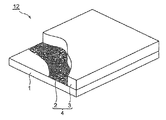
[도 1]차폐부 경계에서의 단선의 메카니즘을 나타내는 도면이다.
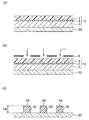
[도 2]감광성 도전 필름의 일 실시형태를 나타내는 모식 단면도이다.
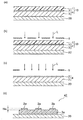
[도 3]감광성 도전 필름의 일 실시형태를 나타내는 일부 절결 사시도이다.
[도 4]감광성 도전 필름을 사용한 도전 패턴 형성 방법의 일 실시형태를 설명하기 위한 모식 단면도이다.
[도 5]감광성 도전 필름을 사용한 도전 패턴의 형성 방법의 다른 실시형태를 설명하기 위한 모식 단면도이다.
[도 6]정전용량식의 터치 패널 센서의 일례를 나타내는 모식 상면도이다.
[도 7]도 6에 나타나는 터치 패널 센서의 제조 방법의 일례를 설명하기 위한 모식도이다.
[도 8]도 6에 나타나는 a-a'선을 따른 부분 단면도이다.
[도 9]도 6에 나타나는 b-b'선을 따른 부분 단면도이다.
[도 10]실시예 1에서 제작한 내광성 시험용의 아웃셀(out cell)형 시료의 평면도이다.
[도 11]실시예 1에서 제작한 내광성 시험용의 아웃셀형 시료의 단면도이다.
[도 12]실시예 11 및 12에서 제작한 내광성 시험용의 커버 유리 일체형(體型) 시료의 평면도이다.
[도 13]실시예 11 및 12에서 제작한 내광성 시험용의 커버 유리 일체형 시료의 단면도이다.
[도 14]실시예 1에서 터치 패널 구동 평가를 위해 제작한 FPC와 접속한 도전 패턴을 가지는 PET 필름 기판의 평면도이다.
[도 15]실시예 1에서 제작한 터치 패널 구동 평가용의 아웃셀형 시료의 단면도이다.
[도 16]실시예 1에서 제작한 터치 패널 구동 평가용의 아웃셀형 시료의 평면도이다.
[도 17]실시예 1에서 제작한 터치 패널 구동 평가용의 장치를 나타내는 도면이다.
[도 18]실시예 11 및 12에서 제작한 터치 패널 구동 평가용의 커버 유리 일체형 시료의 단면도이다.
[도 19]실시예 11 및 12에서 제작한 터치 패널 구동 평가용의 커버 유리 일체형 시료의 평면도이다. 1 is a diagram showing a mechanism of disconnection at a shield boundary;
2 is a schematic cross-sectional view showing one embodiment of a photosensitive conductive film.
3 is a partially cutaway perspective view showing one embodiment of the photosensitive conductive film.
4 is a schematic cross-sectional view for explaining an embodiment of a conductive pattern forming method using a photosensitive conductive film.
5 is a schematic cross-sectional view for explaining another embodiment of a method of forming a conductive pattern using a photosensitive conductive film.
6 is a schematic top view showing an example of a capacitance type touch panel sensor.
7 is a schematic view for explaining an example of a manufacturing method of the touch panel sensor shown in FIG. 6;
8 is a partial cross-sectional view taken along the line a-a 'shown in FIG. 6;
9 is a partial cross-sectional view taken along the line b-b 'shown in FIG. 6;
10 is a plan view of an out cell type sample for light resistance test produced in Example 1. FIG.
11 is a sectional view of an out-cell type sample for light resistance test produced in Example 1. Fig.
12 is a plan view of a cover glass integral body specimen for light resistance test produced in Examples 11 and 12. FIG.
13 is a sectional view of a cover glass integral sample for light resistance test produced in Examples 11 and 12. Fig.
14 is a plan view of a PET film substrate having a conductive pattern connected to an FPC manufactured for evaluation of touch panel drive in
15 is a sectional view of an out-cell type sample for evaluation of a touch panel drive manufactured in Example 1. FIG.
16 is a plan view of an out-cell type sample for evaluation of a touch panel drive manufactured in Example 1. FIG.
[Fig. 17] Fig. 17 is a diagram showing a device for evaluating a touch panel drive manufactured in the first embodiment.
18 is a cross-sectional view of a cover glass integral sample for touch panel drive evaluation produced in Examples 11 and 12. FIG.
19 is a plan view of a cover glass integral sample for evaluation of a touch panel drive manufactured in Examples 11 and 12. FIG.
발명을 실시하기Carrying out the invention 위한 형태 Form for
이하, 본 발명의 적합한 실시형태에 관하여 상세히 설명한다. 또한, 본 명세서에 있어서의 「(메타)아크릴레이트」란, 「아크릴레이트」 및 그에 대응하는 「메타크릴레이트」를 의미한다. 동일하게 「(메타)아크릴산」이란, 「아크릴산」 및 「메타크릴산」을 의미하고, 「(메타)아크릴기」란, 「아크릴기」 및 「메타크릴기」를 의미한다. 또한 「∼」를 이용하여 나타낸 수치 범위는, 「∼」의 전후에 기재되는 수치를 각각 최소값 및 최대값으로서 포함하는 범위를 나타낸다. Hereinafter, a preferred embodiment of the present invention will be described in detail. In the present specification, "(meth) acrylate" means "acrylate" and corresponding "methacrylate". Similarly, the term "(meth) acrylic acid" means "acrylic acid" and "methacrylic acid", and the term "(meth) acrylic group" means "acrylic group" and "methacrylic group". The numerical range indicated by "~" indicates a range including numerical values before and after "~" as a minimum value and a maximum value, respectively.
본 발명자들은, 광조사에 의한 터치 패널의 동작 불량의 원인을 조사하여 동작 불량이 도전 패턴의 저항 상승 또는 단선에 의하는 것이고, 더 구체적으로는 투명 전극재로서 사용한 은나노 와이어의 절단이 원인이다는 것을 확인했다. The present inventors investigated the cause of the operation failure of the touch panel by light irradiation and found that the defective operation was caused by the increase or decrease in the resistance of the conductive pattern and more specifically to the disconnection of the silver wire used as the transparent electrode material Confirmed.
그래서, 광조사 후의 센서 전극을 상세히 조사한 결과, 센서 전극의 저항 상승 또는 단선이 하기 2와 같은 메카니즘으로 발생한다는 것이 판명되었다. 즉, (i) 자외광에 의한 은나노 와이어의 열화(劣化)와, (ii) 가시광에 의한 은나노 와이어의 열화이다. As a result of detailed examination of the sensor electrode after light irradiation, it has been found that the resistance rise or disconnection of the sensor electrode occurs by the
(i) 자외광에 의한 은나노 와이어의 열화 메카니즘은 이하와 같다. 우선, 자외광에 의해 도전 패턴 중에 포함되는 수지 조성물이 분해되어, 최종적으로는 산(아세트산 등)이 생성된다. 이 산이 은나노 와이어를 부식 또는 열화시킨다. 산에 의한 은나노 와이어의 열화가 원인으로, 센서 전극이 저항 상승 또는 단선된다. (i) The deterioration mechanism of silver nano wire by ultraviolet light is as follows. First, the resin composition contained in the conductive pattern is decomposed by ultraviolet light, and finally an acid (such as acetic acid) is produced. These acids corrode or degrade the silver nanowires. Due to the deterioration of the silver nano wire by the acid, the resistance of the sensor electrode is increased or cut.
(ii) 가시광에 의한 은나노 와이어의 열화 메카니즘은, 이하와 같다. 가시광을 은나노 와이어가 흡수하고, 은나노 와이어가 이온화되어 도전 패턴의 수지 조성물 중에 확산된다. 은나노 와이어가 이온화되어 수지 중에 확산됨으로써, 은나노 와이어가 가늘어지고, 최종적으로 단선되어, 센서 전극이 저항 상승 또는 단선된다. (ii) The deterioration mechanism of the silver nanowire by visible light is as follows. The visible light is absorbed by the silver nano wire, and the silver nano wire is ionized and diffused into the resin composition of the conductive pattern. The silver nano wire is ionized and diffused into the resin, whereby the silver nano wire is tapered and finally disconnected, and the sensor electrode is raised or broken.
가시광에 의한 은나노 와이어의 열화는, 자외광과 가시광이 동시에 은나노 와이어에 쬐는 조건에서는 진행하기 어렵고, 자외광이 커트(cut)되고 가시광만이 은나노 와이어에 쬐는 조건에서는, 열화가 진행되기 쉽다. The deterioration of the silver nano wire by visible light is difficult to proceed under the condition that the ultraviolet light and the visible light are irradiated to the silver nano wire at the same time and deteriorates easily under the condition that the ultraviolet light is cut and only the visible light strikes the silver nano wire.
본 발명자들은, 광조사에 의해 저항 상승 또는 단선에 이르른 센서 전극을 조사함으로써, 센서 전극의 단선 개소(箇所)에는, 크게 나누어 2개소 있다는 것을 밝혀냈다. 즉 (1) 뷰 에리어와 (2) 차폐부 경계이다. 특히 스마트 폰이나 태블릿 PC의 경우, 차폐부 경계란, 가식(加飾)인쇄부 등의 차폐부와 뷰 에리어와의 경계인 것이다. 본 발명자들의 다대(多大)한 검토의 결과, (1) 뷰 에리어에서의 단선은, 주로 전술한 (i) 자외광에 의한 은나노 와이어의 열화가 원인으로 발생하고 있다는 것을 밝혀냈다. 또한, (2) 차폐부 경계에서의 단선은, 주로 전술한 (ii) 가시광에서의 열화가 원인으로 발생하고 있다는 것을 발견했다. The inventors of the present invention have found that there are two roughly divided portions of the sensor electrode by irradiating the sensor electrode which has risen or broken by the light irradiation. (1) view area and (2) shield boundary. Particularly, in the case of a smart phone or a tablet PC, the shielding boundary is a boundary between a shielding portion such as a decorative printing portion and a view area. As a result of extensive studies by the inventors of the present invention, it has been found that (1) disconnection in the view area mainly occurs due to deterioration of the silver nanowire caused by (i) ultraviolet light described above. Further, it has been found that (2) the disconnection at the boundary of the shielding portion mainly occurs due to the deterioration in the above-mentioned (ii) visible light.
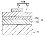
(2) 차폐부 경계에서의 단선의 메카니즘을, 도 1을 이용하여 설명한다. 도 1에 있어서, 102는 터치 화면, 200은 터치 패널, 201은 광 또는 태양광, 202는 자외광, 203은 가시광, 204는 적외광, 210은 OCA(Optically Clear Adhesive), 220은 센서 전극, 221은 은나노 와이어, 230은 기재(基材), 240은 차폐부(가식인쇄부)를 나타낸다. (2) The mechanism of disconnection at the shield boundary will be described with reference to Fig. 1,
우선, 차폐부(240)와 뷰 에리어(102)의 경계에 닿은 광(201)이 차폐부 경계에서 회절된다. 회절의 크기는 광의 파장에 따라 다르기 때문에, 차폐부 경계로부터 센서 전극의 은나노 와이어에 광이 닿기까지, 자외광(202), 가시광(203), 및 적외광(204)으로 분광된다. 즉, 차폐부 경계에서의 센서 전극에는, 분광에 의해 자외광(202)과 가시광(203)이 별개로 닿는 부분이 국소적으로 존재한다. 이 때문에, 분광에 의해 가시광(203)만이 은나노 와이어(221)에 닿는 상태가 되기 때문에, 상기 (ii)의 메카니즘(가시광에 의한 은나노 와이어의 열화)에 의해 은나노 와이어가 열화되어, 센서 전극의 저항 상승 또는 단선이 발생하게 된다. First, the light 201 which is in contact with the boundary between the shielding
본 발명자들은, 상기 발견으로부터, 도전 패턴과 수지층을 포함하는 적층체에 있어서, 크세논 램프로부터 60W/m2(파장 300nm∼400nm의 분광 방사 조도의 적산값)의 조사 강도로 조사를 300시간 받은 부분의 저항 상승률이 20% 이하이면, 단선을 효과적으로 억제할 수 있다는 것을 발견하여, 본 발명에 이르렀다. 또한, 저항 상승률을 20% 이하로 억제하는 구체적인 방법을 발견했다. From the above discovery, the inventors of the present invention have found from the above discovery that a laminate including a conductive pattern and a resin layer is irradiated with a radiation intensity of 60 W / m 2 (integrated value of spectral irradiance with a wavelength of 300 nm to 400 nm) from a xenon lamp for 300 hours And that the disconnection can be effectively suppressed if the rate of increase in the resistance of the portion is 20% or less. Thus, the present invention has been accomplished. In addition, we found a concrete method of suppressing the rate of resistance increase to 20% or less.
본 발명의 적층체는, 기판과, 도전성 섬유와, 수지층을 포함하는 적층체로서, 크세논 램프로부터 60W/m2(파장 300nm∼400nm의 분광 방사 조도의 적산값)의 조사 강도로 조사를 300시간 받은 부분의 저항 상승률이 20% 이하이다. 적층체가 차폐부를 가질 때는, 차폐부의 단부(端部)에서의 저항 상승률도 20% 이하이다. 저항 상승률은, 실시예에 기재된 바와 같이 아웃셀형 샘플 또는 커버 유리 일체형 샘플을 이용하여 측정한다. The laminate of the present invention is a laminate including a substrate, conductive fibers, and a resin layer, and is irradiated from a xenon lamp at an irradiation intensity of 60 W / m 2 (integrated value of spectral irradiance with a wavelength of 300 nm to 400 nm) The rate of increase in resistance at the time of receiving is less than 20%. When the laminate has the shielding portion, the rate of increase in resistance at the end portion of the shielding portion is also 20% or less. The rate of resistance increase is measured using an outsample-type sample or a cover glass-integrated sample as described in the Examples.
이와 같은 적층체는, 이하의 감광성 도전 필름을 사용하여 제조할 수 있다. Such a layered product can be produced by using the following photosensitive conductive film.
예를 들면, 지지 필름 위에, 도전성 섬유를 포함하는 감광층을 구비하고, 상기 감광층이, 바인더 폴리머, 광중합성 화합물, 광중합 개시제에 더하여, 금속 첨가제를 함유하는 감광성 도전 필름을 사용한다. For example, a photosensitive conductive film containing a metal additive in addition to a binder polymer, a photopolymerizable compound, and a photopolymerization initiator is used as the photosensitive layer, provided on the supporting film, with a photosensitive layer containing conductive fibers.
구체적으로는, 기판 위에, 상기 감광성 도전 필름을 라미네이트(전사)하고, 패턴상(狀)으로 활성 광선을 조사하여 노광하고, 감광층의 미노광부를 제거하여, 도전 패턴을 형성한다. 그 결과, 기판 위에 도전 패턴이 설치된 적층체를 얻을 수 있다. 예를 들면, 도 4(c), 도 5(d)와 같이, 도전 패턴은, 수지층과 도전성 섬유를 포함한다. 기판, 수지층, 도전성 섬유의 순으로 배치된다. Specifically, the photosensitive conductive film is laminated (transferred) onto a substrate, and exposed to light by irradiating actinic rays in a pattern, thereby removing the unexposed portion of the photosensitive layer to form a conductive pattern. As a result, a laminate provided with a conductive pattern on a substrate can be obtained. For example, as shown in Figs. 4 (c) and 5 (d), the conductive pattern includes a resin layer and conductive fibers. The substrate, the resin layer, and the conductive fiber are arranged in this order.
금속 첨가제를 포함함으로써, 가시광에 의한 은나노 와이어의 열화 또는 단선을 큰 폭으로 억제할 수 있다. 이는, 은나노 와이어가 가시광을 흡수하는 것으로 얻은 에너지가, 금속 첨가제로 이동함으로써, 은나노 와이어의 입자화, 수지 중으로의 확산이 억제되기 때문이다. By including the metal additive, deterioration or disconnection of the silver nanowire due to visible light can be suppressed to a large extent. This is because the energy obtained by the absorption of the visible light by the silver nano wire moves to the metal additive and the diffusion of the silver nano wire into the resin and diffusion into the resin is suppressed.
또한, 경화 수지층이, 금속 첨가제를 포함함으로써, 자외광에 의한 열화 또는 단선을 억제할 수 있다. 이는, 자외광에 의한 경화 수지층의 분해에 의해 발생한 산과, 금속 첨가제가 반응하여, 산에 의한 은나노 와이어의 열화가 억제되기 때문이라고 추측한다. Further, when the cured resin layer contains a metal additive, deterioration or disconnection due to ultraviolet light can be suppressed. This is presumably because the acid generated by decomposition of the cured resin layer by ultraviolet light reacts with the metal additive and deterioration of the silver nano wire due to the acid is suppressed.
또한, 감광성 도전 필름은, 아민 첨가제를 함유해도 된다. 아민 첨가제에도 내광성을 높이는 작용이 있다. 이는, 자외광에 의한 수지층의 분해에 의해 발생한 산과, 아민이 반응하여 산을 중화함으로써, 산에 의한 은나노 와이어의 열화가 억제되기 때문이라고 추측한다. The photosensitive conductive film may contain an amine additive. The amine additive also has an effect of enhancing the light resistance. This is presumably because the acid generated by the decomposition of the resin layer due to ultraviolet light reacts with the amine to neutralize the acid, and deterioration of the silver nano wire due to the acid is suppressed.
이하, 본 발명에 관하여 상세히 설명한다. Hereinafter, the present invention will be described in detail.
<감광성 도전 필름>≪ Photosensitive conductive film &
본 발명에 관련되는 감광성 도전 필름은, 지지 필름과, 상기 지지 필름 위에 설치된 도전성 섬유를 포함하는 감광층으로 구성된다. 감광성 도전 필름의 일 실시형태를 도 2에 나타낸다. 감광성 도전 필름(10)은, 지지 필름(1)과 감광층(4)으로 이루어지고, 감광층(4)은, 도전막(2)과 감광성 수지층(3)으로 이루어진다. 또한, 감광성 도전 필름은, 도 2에 나타내는 바와 같이, 도전성 섬유를 포함하는 도전막(2)과, 상기 도전막(2) 위에 설치된 감광성 수지층(3)과의 경계가, 명확하게 나누어져 있어도 되지만, 도전막(2)과 감광성 수지층(3)과의 경계는 반드시 명확하게 되어 있지 않아도 된다. 도전막은 감광층의 면방향으로 도전성을 얻을 수 있는 것이면 되고, 도전막에 감광성 수지층이 서로 섞인 태양(態樣)이어도 된다. 예를 들면, 도전막 중에 감광성 수지층을 구성하는 조성물이 함침되어 있거나, 감광성 수지층을 구성하는 조성물이 도전막의 표면에 존재하고 있거나 해도 된다. The photosensitive conductive film according to the present invention is composed of a support film and a photosensitive layer containing conductive fibers provided on the support film. An embodiment of the photosensitive conductive film is shown in Fig. The photosensitive
본 발명의 감광층은, 바인더 폴리머, 광중합성 화합물, 광중합 개시제, 금속 첨가제를 함유하고 있다. 아민 첨가제를 더 포함해도 된다. 또한, 본 발명에 있어서 아민 첨가제는 금속을 포함하지 않는다. 금속 첨가제와 아민 첨가제는, 도전막과 감광성 수지층 중 어느 하나, 또는 그 양쪽에 첨가할 수 있다. The photosensitive layer of the present invention contains a binder polymer, a photopolymerizable compound, a photopolymerization initiator, and a metal additive. An amine additive may be further included. In the present invention, the amine additive does not contain a metal. The metal additive and the amine additive may be added to either or both of the conductive film and the photosensitive resin layer.
이하, 감광성 도전 필름(10)을 구성하는 지지 필름(1), 도전막(2) 및 감광성 수지층(3)의 각각에 관하여 상세히 설명한다. Hereinafter, the
지지 필름(1)으로서는, 폴리에틸렌테레프탈레이트 필름, 폴리에틸렌 필름, 폴리프로필렌 필름, 폴리카보네이트 필름 등의 내열성 및 내용제성을 가지는 중합체 필름을 들 수 있다. 이들 중, 투명성이나 내열성의 관점에서는, 폴리에틸렌테레프탈레이트 필름이 바람직하다. 또한, 이들의 중합체 필름은, 후에 감광층(4)으로부터 제거하기 위해, 제거가 불가능하게 되는 표면 처리가 실시되지 않은 것이 바람직하고, 제거가 불가능하게 되는 재질이 아닌 것이 바람직하다. Examples of the support film (1) include polymer films having heat resistance and solvent resistance, such as polyethylene terephthalate film, polyethylene film, polypropylene film and polycarbonate film. Of these, a polyethylene terephthalate film is preferable from the viewpoints of transparency and heat resistance. Further, it is preferable that these polymer films are not subjected to surface treatment which makes it impossible to remove them in order to remove them from the
또한, 지지 필름(1)의 두께는, 5∼300㎛인 것이 바람직하고, 10∼200㎛인 것이 보다 바람직하고, 15∼100㎛인 것이 특히 바람직하다. 기계적 강도가 저하되어, 도전막(2)을 형성하기 위해서 도전성 분산액 혹은 감광성 수지층(3)을 형성하기 위해서 감광성 수지 조성물을 도공(塗工)하는 공정, 또는 노광한 감광성 수지층(3)을 현상하기 전에 지지 필름을 박리하는 공정에 있어서, 지지 필름이 찢어지는 것을 방지하는 관점에서, 5㎛ 이상인 것이 바람직하고, 10㎛ 이상인 것이 보다 바람직하고, 15㎛ 이상인 것이 더욱 바람직하다. 또한, 지지 필름을 통하여 활성 광선을 감광성 수지층에 조사 후의 패턴의 해상도가 뛰어나는 점에서는, 300㎛ 이하인 것이 바람직하고, 200㎛ 이하인 것이 보다 바람직하고, 100㎛ 이하인 것이 더욱 바람직하다. The thickness of the
지지 필름(1)의 헤이즈값은, 감도 및 해상도를 양호하게 할 수 있는 관점에서, 0.01∼5.0%인 것이 바람직하고, 0.01∼3.0%인 것이 보다 바람직하고, 0.01∼2.0%인 것이 더욱 바람직하고, 0.01∼1.0%인 것이 특히 바람직하다. 또한, 헤이즈값은 JIS K 7375(2008년 제정)에 준거하여 측정할 수 있다. 또한, NDH-1001DP(일본전색공업(주)제, 상품명) 등의 시판의 탁도계 등으로도 측정 가능하다. The haze value of the
도전막(2)은, 도전성 섬유로서 금,은, 구리, 백금 등의 금속 섬유 또는 카본 나노 튜브 등의 탄소섬유 등을 들 수 있지만, 본 발명은 은나노 와이어를 포함하는 도전성 섬유를 사용했을 때에 효과를 나타낸다. As the
도 3은, 감광성 도전 필름의 일 실시형태를 나타내는 일부 절결 사시도이다. 도전막(2)은, 도 3에 나타내는 바와 같이, 도전성 섬유끼리가 접촉해서 이루어지는 망목(網目) 구조를 가지는 것이 바람직하다. 이러한 망목 구조를 가지는 도전막(2)은, 감광성 수지층(3)의 지지 필름(1) 측의 표면에 형성되어 있어도 되지만, 지지 필름(1)을 박리했을 때에 노출되는 감광층(4)의 표면에 있어서 그 면방향으로 도전성을 얻을 수 있다면, 도전막(2)에 감광성 수지층(3)의 일부가 들어가는 형태로 형성되어 있어도 되며, 감광성 수지층(3)의 지지 필름(1) 측의 표층에 도전막(2)이 포함되는 형태로 형성되어 있어도 된다. 3 is a partially cutaway perspective view showing an embodiment of the photosensitive conductive film. As shown in Fig. 3, the
상기의 은나노 와이어를 포함하는 도전성 섬유는, 예를 들면, 은이온을 NaBH4 등의 환원제로 환원하는 방법, 또는 폴리올법에 의해 조제할 수 있다. The conductive fiber containing the silver nanowire can be prepared by, for example, a method of reducing silver ions with a reducing agent such as NaBH 4 or a polyol method.
도전성 섬유의 섬유 지름은, 1nm∼50nm인 것이 바람직하고, 2nm∼20nm인 것이 보다 바람직하고, 3nm∼10nm인 것이 더욱 바람직하다. 또한, 도전성 섬유의 섬유 길이는, 1㎛∼100㎛인 것이 바람직하고, 2㎛∼50㎛인 것이 보다 바람직하고, 3㎛∼10㎛인 것이 더욱 바람직하다. 섬유 지름 및 섬유 길이는, 주사형 전자현미경에 의해 측정할 수 있다. The fiber diameter of the conductive fiber is preferably 1 nm to 50 nm, more preferably 2 nm to 20 nm, and even more preferably 3 nm to 10 nm. The fiber length of the conductive fiber is preferably 1 m to 100 m, more preferably 2 m to 50 m, and even more preferably 3 m to 10 m. The fiber diameter and fiber length can be measured by a scanning electron microscope.
또한, 상기 도전막(2)에는, 도전성 섬유와 함께 유기 도전체를 사용할 수 있다. 유기 도전체로서는, 특별히 제한 없이 사용할 수 있지만, 티오펜 유도체나 아닐린 유도체의 폴리머 등의 유기 도전체를 사용하는 것이 바람직하다. An organic conductor may be used for the
구체적으로는, 폴리에틸렌디옥시티오펜, 폴리헥실티오펜이나 폴리아닐린, 폴리비닐피롤리돈 등을 사용할 수 있다. Specifically, polyethylene dioxythiophene, polyhexylthiophene, polyaniline, polyvinylpyrrolidone, and the like can be used.
도전막(2)의 두께는, 본 발명의 감광성 도전 필름을 사용하여 형성되는 도전 패턴의 용도나 요구되는 도전성에 따라 다르지만, 1㎛ 이하인 것이 바람직하고, 1nm∼0.5㎛인 것이 보다 바람직하고, 5nm∼0.1㎛인 것이 더욱 바람직하다. 도전막(2)의 두께가 1 이하이면, 450∼650nm의 파장역에서의 광투과율이 높고, 패턴 형성성도 뛰어나고, 특히 투명 전극의 제작에 적합한 것이 된다. 또한, 도전막(2)의 두께는, 주사형 전자현미경 사진에 의해 측정되는 값을 가리킨다. The thickness of the
도전막(2)은, 예를 들면, 지지 필름(1) 위에, 상술한 도전성 섬유나 유기 도전체를 물 및/또는 유기용제와, 계면활성제 등의 분산 안정제 등을 첨가한 도전성 분산액을 도공한 후, 건조함으로써 형성할 수 있다. 건조 후, 지지 필름(1) 위에 형성한 도전막(2)은, 필요에 따라 라미네이트 되어도 된다. The
도공은, 롤 코트법, 콤마 코트법, 그라비아 코트법, 에어 나이프 코트법, 다이 코트법, 바 코트법, 스프레이 코트법 등의 공지된 방법으로 실시할 수 있다. 또한, 건조는, 30∼150℃에서 1∼30분간 정도, 열풍 대류식 건조기 등으로 실시할 수 있다. 도전막(2)에 있어서, 도전성 섬유나 유기 도전체는 계면활성제나 분산 안정제와 공존하고 있어도 상관없다. The coating can be carried out by a known method such as a roll coating method, a comma coating method, a gravure coating method, an air knife coating method, a die coating method, a bar coating method, and a spray coating method. The drying can be carried out at 30 to 150 DEG C for about 1 to 30 minutes in a hot air convection type dryer or the like. In the
상기 도전성 분산액에는, 필요에 따라 금속 첨가제, 아민 첨가제를 첨가할 수 있다. 이에 의해, 도전성 분산액을 도공 및 건조함으로써 형성한 도전막을 포함하는 도전 패턴에, 금속 첨가제, 아민 첨가제를 함유시킬 수 있다. To the conductive dispersion, a metal additive and an amine additive may be added as necessary. Thereby, a metal additive and an amine additive can be contained in the conductive pattern including the conductive film formed by coating and drying the conductive dispersion.
감광성 수지층(3)으로서는, (A) 바인더 폴리머, (B) 광중합성 화합물, (C) 광중합 개시제를 함유하는 감광성 수지 조성물로 형성되는 것을 들 수 있다. 상기의 감광성 수지 조성물은, (D) 금속 첨가제 및/또는(E) 아민 첨가제를 포함할 수 있다. Examples of the
(A) 바인더 폴리머로서는, 아크릴 수지, 스티렌 수지, 에폭시 수지, 아미드 수지, 아미드에폭시 수지, 알키드 수지, 페놀 수지, 에스테르 수지, 우레탄 수지, 에폭시 수지와 (메타)아크릴산의 반응으로 얻어지는 에폭시아크릴레이트 수지, 에폭시아크릴레이트 수지와 산무수물의 반응으로 얻어지는 산변성 에폭시아크릴레이트 수지 등을 들 수 있다. 이들의 수지는, 단독으로 또는 2종 이상을 조합하여 사용할 수 있다. Examples of the binder polymer (A) include an epoxy resin, an epoxy resin, an amide epoxy resin, an alkyd resin, a phenol resin, an ester resin, a urethane resin, an epoxy acrylate resin obtained by the reaction of an epoxy resin and (meth) acrylic acid , And acid-modified epoxy acrylate resins obtained by the reaction of an epoxy acrylate resin and an acid anhydride. These resins may be used alone or in combination of two or more.
상기 중에서도, 알칼리 현상성 및 필름 형성성이 뛰어나는 관점에서, 아크릴 수지를 사용하는 것이 바람직하고, 그 아크릴 수지가 (메타)아크릴산 및 (메타)아크릴산알킬에스테르에서 유래하는 모노머 단위를 구성 단위로서 가지면 보다 바람직하다. 여기서, 「아크릴 수지」란, (메타)아크릴기를 가지는 중합성 단량체에서 유래하는 모노머 단위를 주로 가지는 중합체를 의미한다. Above all, it is preferable to use an acrylic resin from the viewpoint of excellent alkali developability and film formability. When the acrylic resin has a monomer unit derived from (meth) acrylic acid and (meth) acrylic acid alkyl ester as a constituent unit More preferable. Here, "acrylic resin" means a polymer having mainly a monomer unit derived from a polymerizable monomer having a (meth) acrylic group.
상기 아크릴 수지는, (메타)아크릴기를 가지는 중합성 단량체를 라디칼 중합하여 제조되는 것을 사용할 수 있다. As the acrylic resin, those produced by radical polymerization of a polymerizable monomer having a (meth) acrylic group can be used.
상기 (메타)아크릴기를 가지는 중합성 단량체로서는, 디아세톤아크릴아미드 등의 아크릴아미드;(메타)아크릴산알킬에스테르, 2-히드록시알킬(메타)아크릴레이트, (메타)아크릴산테트라히드로푸르푸릴에스테르, (메타)아크릴산디메틸아미노에틸에스테르, (메타)아크릴산디에틸아미노에틸에스테르, (메타)아크릴산글리시딜에스테르, 2,2,2-트리플루오로에틸(메타)아크릴레이트, 2,2,3,3-테트라플루오로프로필(메타)아크릴레이트 등의 (메타)아크릴산에스테르;(메타)아크릴산, α-브로모(메타)아크릴산, α-크롤(메타)아크릴산, β-푸릴(메타)아크릴산, β-스티릴(메타)아크릴산 등의 (메타)아크릴산 등을 들 수 있다.Examples of the polymerizable monomer having a (meth) acrylic group include acrylamide such as diacetone acrylamide, alkyl (meth) acrylate, 2-hydroxyalkyl (meth) acrylate, tetrahydrofurfuryl (meth) (Meth) acrylic acid dimethylaminoethyl ester, diethylaminoethyl (meth) acrylate, glycidyl (meth) acrylate, 2,2,2-trifluoroethyl (Meth) acrylic acid esters such as (meth) acrylic acid,? -Bromo (meth) acrylic acid,? -Chlor (meth) acrylic acid, (Meth) acrylic acid such as styryl (meth) acrylic acid and the like.
또한, 상기 아크릴 수지는, 상기와 같은 (메타)아크릴기를 가지는 중합성 단량체 외에, 스티렌 유도체, 아크릴로니트릴, 비닐-n-부틸에테르 등의 비닐알코올의 에스테르류, 말레산, 말레산무수물, 말레산모노메틸, 말레산모노에틸, 말레산모노이소프로필 등의 말레산모노에스테르, 푸말산, 계피산, α-시아노계피산, 이타콘산, 크로톤산 등의 1종 또는 2종 이상의 중합성 단량체가 공중합되어 있어도 된다. In addition to the above-mentioned polymerizable monomers having a (meth) acrylic group, the acrylic resin may also include esters of vinyl alcohols such as styrene derivatives, acrylonitrile and vinyl-n-butyl ether, maleic acid, maleic anhydride, At least one polymerizable monomer such as maleic acid monoester such as monomethyl maleate, monoethyl maleate, monoisopropyl maleate, fumaric acid, cinnamic acid,? -Cyano cinnamic acid, itaconic acid, crotonic acid, .
상기 (메타)아크릴산알킬에스테르로서는, (메타)아크릴산메틸에스테르, (메타)아크릴산에틸에스테르, (메타)아크릴산프로필에스테르, (메타)아크릴산부틸에스테르, (메타)아크릴산헥실에스테르, (메타)아크릴산헵틸에스테르, (메타)아크릴산옥틸에스테르, (메타)아크릴산2-에틸헥실에스테르, (메타)아크릴산노닐에스테르를 들 수 있다. 이들은, 단독으로 또는 2종 이상을 조합하여 사용할 수 있다. Examples of the alkyl (meth) acrylate ester include (meth) acrylic acid methyl ester, (meth) acrylic acid ethyl ester, (meth) acrylic acid propyl ester, (meth) acrylic acid butyl ester, (meth) acrylic acid hexyl ester, , Octyl (meth) acrylate, 2-ethylhexyl (meth) acrylate and nonyl (meth) acrylate. These may be used alone or in combination of two or more.
또한, (A) 바인더 폴리머는, 알칼리 현상성을 보다 양호하게 하는 관점에서, 카르복실기를 가지는 것이 바람직하다. 카르복실기를 가지는 중합성 단량체로서는, 상술한 바와 같은 (메타)아크릴산을 들 수 있다. Further, the binder polymer (A) preferably has a carboxyl group from the viewpoint of improving the alkali developability. As the polymerizable monomer having a carboxyl group, there may be mentioned (meth) acrylic acid as described above.
(A) 바인더 폴리머가 가지는 카르복실기의 비율은, 사용하는 전체 중합성 단량체에 대한 카르복실기를 가지는 중합성 단량체의 비율로서, 10∼50질량%인 것이 바람직하고, 12∼40질량%인 것이 보다 바람직하고, 15∼30질량%인 것이 더욱 바람직하고, 15∼25질량%인 것이 특히 바람직하다. 알칼리 현상성이 뛰어나는 점에서는 10질량% 이상인 것이 바람직하고, 알칼리 내성이 뛰어나는 점에서는, 50질량% 이하인 것이 바람직하다. The proportion of the carboxyl group of the binder polymer (A) is preferably from 10 to 50% by mass, more preferably from 12 to 40% by mass, in terms of the proportion of the polymerizable monomer having a carboxyl group to the entire polymerizable monomer to be used , More preferably from 15 to 30 mass%, and particularly preferably from 15 to 25 mass%. It is preferably 10 mass% or more in view of excellent alkali developability, and is preferably 50 mass% or less from the viewpoint of excellent alkali resistance.
(A) 바인더 폴리머의 중량평균분자량은, 기계 강도 및 알칼리 현상성의 밸런스를 도모하는 관점에서, 5000∼300000인 것이 바람직하고, 20000∼150000인 것이 보다 바람직하고, 30000∼100000인 것이 더욱 바람직하다. 내현상액성이 뛰어나는 점에서는, 중량평균분자량이, 5000 이상인 것이 바람직하다. 또한, 현상 시간의 관점에서는, 300000 이하인 것이 바람직하다. 또한, 본 발명에 있어서의 중량평균분자량은, 겔 침투 크로마토그래피법(GPC)에 의해 측정되고, 표준 폴리스티렌을 사용하여 작성한 검량선에 의해 환산된 값이다. The weight average molecular weight of the binder polymer (A) is preferably from 5,000 to 300,000, more preferably from 20,000 to 150,000, and even more preferably from 30,000 to 100,000 from the viewpoint of balance of mechanical strength and alkali developability. It is preferable that the weight average molecular weight is 5000 or more in view of excellent resistance to developing. Further, from the viewpoint of developing time, it is preferably 300000 or less. The weight average molecular weight in the present invention is a value measured by gel permeation chromatography (GPC) and converted by a calibration curve prepared using standard polystyrene.
다음으로, (B) 광중합성 화합물에 관하여 설명한다. 광중합성 화합물은 에틸렌성 불포화 결합을 가지는 것이 바람직하다. Next, the photopolymerizable compound (B) will be described. The photopolymerizable compound preferably has an ethylenic unsaturated bond.
에틸렌성 불포화 결합을 가지는 광중합성 화합물로서는, 2,2-비스(4-((메타)아크릴록시폴리에톡시)페닐)프로판, 2,2-비스(4-((메타)아크릴록시폴리프로폭시)페닐)프로판, 2,2-비스(4-((메타)아크릴록시폴리에톡시폴리프로폭시)페닐)프로판 등의 비스페놀A디(메타)아크릴레이트 화합물;폴리에틸렌글리콜디(메타)아크릴레이트, 폴리프로필렌글리콜디(메타)아크릴레이트, 폴리에틸렌폴리프로필렌글리콜디(메타)아크릴레이트 등의 폴리알킬렌글리콜디(메타)아크릴레이트;트리메틸올프로판디(메타)아크릴레이트, 트리메틸올프로판트리(메타)아크릴레이트, 트리메틸올프로판에톡시트리(메타)아크릴레이트, 트리메틸올프로판트리에톡시트리(메타)아크릴레이트 등의 트리메틸올프로판(메타)아크릴레이트;테트라메틸올메탄트리(메타)아크릴레이트, 테트라메틸올메탄테트라(메타)아크릴레이트 등의 테트라메틸올메탄(메타)아크릴레이트;디펜타에리트리톨펜타(메타)아크릴레이트, 디펜타에리트리톨헥사(메타)아크릴레이트 등의 디펜타에리트리톨(메타)아크릴레이트, 우레탄모노머 등을 들 수 있다. Examples of the photopolymerizable compound having an ethylenically unsaturated bond include 2,2-bis (4 - ((meth) acryloxypolyethoxy) phenyl) propane, 2,2- (Meth) acrylate compounds such as polyethylene glycol di (meth) acrylate compounds such as polyethylene glycol di (meth) acrylate compounds such as diethylene glycol di (meth) acrylate, dipentaerythritol hexa (Meth) acrylate such as polypropylene glycol di (meth) acrylate and polyethylene polypropylene glycol di (meth) acrylate, trimethylolpropane di (meth) acrylate, trimethylolpropane tri (Meth) acrylate such as trimethylolpropane tri (meth) acrylate, trimethylolpropane ethoxy tri (meth) acrylate and trimethylol propane triethoxy tri (meth) acrylate, tetramethylol methane tri Dipentaerythritol (meth) acrylate such as dipentaerythritol penta (meth) acrylate, dipentaerythritol hexa (metha) acrylate, and the like; Acrylate, urethane monomer, and the like.
(B) 광중합성 화합물의 함유 비율은, 바인더 폴리머 및 광중합성 화합물의 합계 100질량%에 대하여, 30∼80질량%인 것이 바람직하고, 40∼70질량%인 것이 보다 바람직하다. 광경화성 및 전사한 도전막(도전막 및 감광성 수지층)의 도막성이 뛰어나는 점에서는, 30질량% 이상인 것이 바람직하고, 필름으로서 감아 권취했을 경우의 보관 안정성이 뛰어나는 점에서는, 80질량% 이하인 것이 바람직하다. The content of the photopolymerizable compound (B) is preferably 30 to 80 mass%, more preferably 40 to 70 mass%, based on 100 mass% of the total of the binder polymer and the photopolymerizable compound. It is preferably 30% by mass or more in view of excellent photocurability and film properties of the transferred conductive film (conductive film and photosensitive resin layer), and is preferably 80% by mass or more in view of excellent storage stability when the film is rolled up as a film, Or less.
다음으로 (C) 광중합 개시제에 관하여 설명한다. 광중합 개시제로서는, 사용하는 노광기의 광파장과, 기능 발현에 필요한 파장이 맞는 것을 선택하면, 특별히 제한은 없지만, 벤조페논, N,N'-테트라메틸-4,4'-디아미노벤조페논(미히라케톤), N,N'-테트라에틸-4,4'-디아미노벤조페논, 4-메톡시-4'-디메틸아미노벤조페논, 2-벤질-2-디메틸아미노-1-(4-모르폴리노페닐)-부탄온-1, 2-메틸-1-[4-(메틸티오)페닐]-2-모르폴리노-프로판온-1 등의 방향족 케톤;벤조인메틸에테르, 벤조인에틸에테르, 벤조인페닐에테르 등의 벤조인에테르 화합물;벤조인, 메틸벤조인, 에틸벤조인 등의 벤조인 화합물;1,2-옥탄디온-1-[4-(페닐티오)페닐]-2-(0-벤조일옥심), 1-[9-에틸-6-(2-메틸벤조일)-9H-카르바졸-3-일]에탄온1-(O-아세틸옥심) 등의 옥심에스테르 화합물;벤질디메틸케탈 등의 벤질 유도체;2-(o-클로로페닐)-4,5-디페닐이미다졸 이량체, 2-(o-클로로페닐)-4,5-디(메톡시페닐)이미다졸 이량체, 2-(o-플루오로페닐)-4,5-디페닐이미다졸 이량체, 2-(o-메톡시페닐)-4,5-디페닐이미다졸 이량체, 2-(p-메톡시페닐)-4,5-디페닐이미다졸 이량체 등의 2,4,5-트리아릴이미다졸 이량체;9-페닐아크리딘, 1,7-비스(9,9'-아크리디닐)헵탄 등의 아크리딘 유도체;N-페닐글리신, N-페닐글리신 유도체, 옥사졸계 화합물 등을 들 수 있다. Next, the photopolymerization initiator (C) will be described. The photopolymerization initiator is not particularly limited as long as the photopolymerization initiator is selected so that the wavelength of the photopolymerization initiator to be used matches the wavelength required for the functionalization. However, the photopolymerization initiator is preferably selected from the group consisting of benzophenone, N, N'-tetramethyl-4,4'-diaminobenzophenone Ketone), N, N'-tetraethyl-4,4'-diaminobenzophenone, 4-methoxy-4'-dimethylaminobenzophenone, 2- Methyl-1- [4- (methylthio) phenyl] -2-morpholino-propanone-1; benzoin methyl ether, benzoin ethyl ether, Benzoin ether compounds such as benzoin phenyl ether; benzoin compounds such as benzoin, methyl benzoin and ethyl benzoin; 1,2-octanedione-1- [4- (phenylthio) phenyl] -2- Oxime ester compounds such as 1- [9-ethyl-6- (2-methylbenzoyl) -9H-carbazol-3-yl] ethanone 1- (O-acetyloxime), benzyl dimethyl ketal Benzyl derivatives of 2- (o-chlorophenyl) -4,5-diphenylimidazole dimer, 2- (o-fluorophenyl) -4,5-diphenylimidazole dimer, 2- (o-chlorophenyl) -4,5-di (methoxyphenyl) imidazole dimer, 2- -Methoxyphenyl) -4,5-diphenylimidazole dimer, and 2- (p-methoxyphenyl) -4,5-diphenylimidazole dimer. Acridine derivatives such as 9-phenylacridine and 1,7-bis (9,9'-acridinyl) heptane, N-phenylglycine, N-phenylglycine derivatives, .
이들 중에서도, 투명성, 및 10㎛ 이하에서의 패턴 형성능으로부터, 옥심에스테르 화합물이 바람직하다. 옥심에스테르 화합물로서는, 하기 일반식(C-1) 및 일반식(C-2)로 표시되는 화합물을 들 수 있다. 속경화성, 투명성의 관점에서, 하기 일반식(C-1)로 표시되는 화합물이 바람직하다. Of these, oxime ester compounds are preferable from the viewpoints of transparency and pattern forming ability at 10 탆 or less. Examples of the oxime ester compound include compounds represented by the following formulas (C-1) and (C-2). From the viewpoints of fast curability and transparency, a compound represented by the following general formula (C-1) is preferable.

상기 일반식(C-1) 중, R1은, 탄소수 1∼12의 알킬기, 또는 탄소수 3∼20의 시클로알킬기를 나타낸다. 그 중에서도, 탄소수 3∼9의 알킬기가 바람직하다. In the general formula (C-1), R 1 represents an alkyl group having 1 to 12 carbon atoms or a cycloalkyl group having 3 to 20 carbon atoms. Among them, an alkyl group having 3 to 9 carbon atoms is preferable.
또한, 본 발명의 효과를 저해하지 않는 한, 상기 일반식(C-1) 중의 방향환에 치환기를 가지고 있어도 된다. 치환기로서는, 수소 원자 또는 탄소수 1∼12의 알킬기를 들 수 있다. Unless the effect of the present invention is not impaired, the aromatic ring in the general formula (C-1) may have a substituent. Examples of the substituent include a hydrogen atom or an alkyl group having 1 to 12 carbon atoms.

상기 일반식(C-2) 중, R2는 수소 원자 또는 탄소수 1∼12의 알킬기를 나타내고, R3은, 탄소수 1∼12의 알킬기, 또는 탄소수 3∼20의 시클로알킬기를 나타내고, R4는, 탄소 1∼12의 알킬기를 나타내고, R5는, 탄소수 1∼20의 알킬기 또는 아릴기를 나타낸다. p1은 0∼3의 정수를 나타낸다. 또한, p1이 2이상인 경우, 복수의 R4는 각각 동일해도 상이해도 된다. 또한, 카르바졸 위에는 본 발명의 효과를 저해하지 않는 범위에서 치환기를 가지고 있어도 된다. 치환기로서는, 수소 원자 또는 탄소수 1∼12의 알킬기를 들 수 있다. R 2 represents a hydrogen atom or an alkyl group having 1 to 12 carbon atoms; R 3 represents an alkyl group having 1 to 12 carbon atoms or a cycloalkyl group having 3 to 20 carbon atoms; R 4 represents a hydrogen atom or an alkyl group having 1 to 12 carbon atoms; , An alkyl group having 1 to 12 carbon atoms, and R 5 is an alkyl group having 1 to 20 carbon atoms or an aryl group. p1 represents an integer of 0 to 3; When p1 is 2 or more, plural R 4 s may be the same or different. The carbazole may have a substituent on the carbazole moiety to the extent that the effect of the present invention is not impaired. Examples of the substituent include a hydrogen atom or an alkyl group having 1 to 12 carbon atoms.
상기 일반식(C-2) 중, R2 또는 R4는 탄소수 1∼12의 알킬기인 것이 바람직하고, 탄소수 1∼8의 알킬기인 것이 보다 바람직하고, 탄소수 1∼4의 알킬기인 것이 더욱 바람직하다. In the general formula (C-2), R 2 or R 4 is preferably an alkyl group having 1 to 12 carbon atoms, more preferably an alkyl group having 1 to 8 carbon atoms, further preferably an alkyl group having 1 to 4 carbon atoms .
상기 일반식(C-2) 중, R3은 탄소수 1∼8의 알킬기, 또는 탄소수 4∼15의 시클로알킬기인 것이 바람직하고, 탄소수 1∼4의 알킬기, 또는 탄소수 4∼10의 시클로알킬기인 것이 보다 바람직하고, 메틸기, 에틸기인 것이 특히 바람직하다. In the general formula (C-2), R 3 is preferably an alkyl group having 1 to 8 carbon atoms or a cycloalkyl group having 4 to 15 carbon atoms, more preferably an alkyl group having 1 to 4 carbon atoms or a cycloalkyl group having 4 to 10 carbon atoms More preferably a methyl group or an ethyl group.
상기 일반식(C-2) 중, R5는 탄소수 1∼12의 알킬기 또는 탄소수 6∼16의 아릴기인 것이 바람직하고, 탄소수 1∼8의 알킬기 또는 탄소수 6∼14의 아릴기인 것이 보다 바람직하고, 탄소수 1∼4의 알킬기 또는 탄소수 6∼12의 아릴기인 것이 더욱 바람직하다. In the general formula (C-2), R 5 is preferably an alkyl group having 1 to 12 carbon atoms or an aryl group having 6 to 16 carbon atoms, more preferably an alkyl group having 1 to 8 carbon atoms or an aryl group having 6 to 14 carbon atoms, More preferably an alkyl group having 1 to 4 carbon atoms or an aryl group having 6 to 12 carbon atoms.
상기 일반식(C-1)로 표시되는 화합물로서는, 1,2-옥탄디온, 1-[4-(페닐티오)-페닐, 2-(o-벤조일옥심)] 등을 들 수 있다. 상기 일반식(C-2)로 표시되는 화합물로서는, 에탄온, 1-[9-에틸-6-(2-메틸벤조일)-9H-카르바졸-3-일]-, 1-(0-아세틸옥심) 등을 들 수 있다. 1,2-옥탄디온, 1-[4-(페닐티오)-페닐, 2-(0-벤조일옥심)]은, lRGACURE OXE O1(BASF(주)제, 상품명)로서 입수 가능하다. 또한, 에탄온, 1-[9-에틸-6-(2-메틸벤조일)-9H-카르바졸-3-일]-, 1-(O-아세틸옥심)은, lRGACURE OXE O2(BASF(주)제, 상품명)로서 상업적으로 입수 가능하다. 이들은 단독으로, 또는 2종류 이상을 조합하여 사용된다. Examples of the compound represented by the above general formula (C-1) include 1,2-octanedione, 1- [4- (phenylthio) -phenyl, 2- (o-benzoyloxime)] and the like. Examples of the compound represented by the general formula (C-2) include ethanone, 1- [9-ethyl-6- (2-methylbenzoyl) -9H-carbazol- Oxime), and the like. 1,2-octanedione, 1- [4- (phenylthio) -phenyl, 2- (0-benzoyloxime)] are available as lRGACURE OXE O1 (trade name, manufactured by BASF). Further, 1 - [9-ethyl-6- (2-methylbenzoyl) -9H-carbazol-3-yl] -, 1- (O- , ≪ / RTI > trade name). These may be used alone or in combination of two or more.
상기 일반식(1) 중에서도, 특히 1,2-옥탄디온, 1-[4-(페닐티오)-페닐, 2-(O-벤조일옥심)]이 특히 바람직하다. Particularly preferred among the above general formula (1) are 1,2-octanedione, 1- [4- (phenylthio) -phenyl, 2- (O-benzoyloxime)].
광중합 개시제의 함유 비율은, 바인더 폴리머 및 광중합성 화합물의 합계 100질량부에 대하여, 0.1∼20질량부인 것이 바람직하고, 1∼10질량부인 것이 보다 바람직하고, 1∼5질량부인 것이 특히 바람직하다. 광감도가 뛰어나는 점에서는, 0.1질량부 이상인 것이 바람직하고, 광경화성이 뛰어나는 점에서는, 20질량부 이하인 것이 바람직하다. The content of the photopolymerization initiator is preferably 0.1 to 20 parts by mass, more preferably 1 to 10 parts by mass, particularly preferably 1 to 5 parts by mass, based on 100 parts by mass of the total of the binder polymer and the photopolymerizable compound. From the viewpoint of excellent photosensitivity, it is preferably at least 0.1 part by mass, and it is preferably at most 20 parts by mass from the viewpoint of excellent photocurability.
다음으로 (D) 금속 첨가제에 관하여 설명한다. 금속 첨가제는 금속을 포함하는 첨가제이며, 금속 첨가제로서는, 특별히 제한은 없지만, 감광성 도전 필름의 투명성의 점에서 금속 입자, 금속 산화물 입자, 금속 착체 화합물이 바람직하다. 투명성이 나쁘면, 감광성 도전 필름으로 도전 패턴을 형성할 때, 노광시에 광이 산란하거나, 광이 저부(底部)까지 두루 미치지 않거나 하여, 도전 패턴의 형성 불량이 발생한다. Next, (D) the metal additive will be described. The metal additive is an additive containing a metal. The metal additive is not particularly limited, but from the viewpoint of transparency of the photosensitive conductive film, metal particles, metal oxide particles, and metal complex compounds are preferable. When the transparency is poor, when the conductive pattern is formed with the photosensitive conductive film, light is scattered at the time of exposure, or the light does not extend all the way to the bottom, resulting in formation of a defective conductive pattern.
금속 산화물 입자로서는, 산화알루미늄 입자, 산화티탄 입자, 산화지르코늄 입자 등을 들 수 있다. 금속 산화물로서는, 특별히 제한은 없지만, 감광성 도전 필름의 투명성의 점에서, 일차 입자 지름이 100nm 이하인 것이 바람직하다. 또한, 금속 산화물 입자 중에서도, 입수의 용이함, 가격 및 가시광에 의한 은나노 와이어의 열화를 효과적으로 억제할 수 있는 점에서, 산화 티탄 입자가 특히 바람직하다. Examples of the metal oxide particles include aluminum oxide particles, titanium oxide particles, and zirconium oxide particles. The metal oxide is not particularly limited, but from the viewpoint of transparency of the photosensitive conductive film, it is preferable that the primary particle diameter is 100 nm or less. Of the metal oxide particles, titanium oxide particles are particularly preferable because they can be easily obtained, and can effectively inhibit the deterioration of silver nano wires due to price and visible light.
본 발명에 있어서의 (D) 금속 첨가제는, 감광성 수지 중으로의 용해성의 관점에서, 금속 착체 화합물이 바람직하다. 금속 착체가 감광성 도전 필름 중에 포함됨으로써, 가시광에 의한 은나노 와이어의 열화 또는 단선을, 큰 폭으로 억제할 수 있다. The metal additive (D) in the present invention is preferably a metal complex compound from the viewpoint of solubility in a photosensitive resin. By including the metal complex in the photosensitive conductive film, deterioration or disconnection of the silver nano wire due to visible light can be suppressed to a large extent.
금속 착체 화합물은, 하기 일반식(2)로 표시되는 화합물이 바람직하다. The metal complex compound is preferably a compound represented by the following general formula (2).

식(2)에 있어서, Ml은, 알루미늄, 티탄 또는 지르코늄의 금속 원자이며, 감광성 도전 필름의 미경화물의 안정성의 관점에서는, 티탄이 바람직하다. 또한, 감광성 도전 필름의 투명성의 관점에서는, 지르코늄, 알루미늄이 바람직하다. 티탄을 사용했을 경우, 노랗게 착색되는 데 대하여, 지르코늄, 알루미늄은 착색되기 어려워 투명성이 높다. In the formula (2), M 1 is a metal atom of aluminum, titanium or zirconium, and titanium is preferable from the viewpoint of stability of the uncured product of the photosensitive conductive film. From the viewpoint of transparency of the photosensitive conductive film, zirconium and aluminum are preferable. When titanium is used, yellow is colored, whereas zirconium and aluminum are difficult to be colored, so that transparency is high.
m은 0∼4까지의 정수이며, n은 0∼4까지의 정수이며, m과 n의 합은 3 또는 4( Ml이 알루미늄일 때는 3, 티탄 또는 지르코늄일 때는 4이고, 이하 동일)이다. m is an integer of 0 to 4, n is an integer of 0 to 4, and the sum of m and n is 3 or 4 (when M 1 is aluminum, 3 is 3 and when titanium or zirconium is 4, .
안정성의 관점에서, m이 0∼2인 것이 바람직하고, n이 1∼4인 것이 바람직하다. From the viewpoint of stability, m is preferably 0 to 2, and n is preferably 1 to 4.
R5는, 각각 독립하여 탄소수 1∼18(바람직하게는 탄소수 1∼8, 보다 바람직하게는 탄소수 1∼6)의 알킬기를 나타낸다. 탄소수 1∼18의 알킬기는, 구체적으로는 메틸기, 에틸기, n-프로필기, 이소프로필기, n-부틸기, n-헥실기, n-헵틸기, n-데실기, n-도데실기 등을 들 수 있다. 보존 안정성의 관점에서, 이소프로필기인 것이 바람직하다.Each R 5 independently represents an alkyl group having 1 to 18 carbon atoms (preferably 1 to 8 carbon atoms, more preferably 1 to 6 carbon atoms). Specific examples of the alkyl group having 1 to 18 carbon atoms include methyl, ethyl, n-propyl, isopropyl, n-butyl, n-hexyl, . From the viewpoint of storage stability, an isopropyl group is preferable.
R6은, 각각 독립하여 1가의 유기기이며, 상기 1가의 유기기는, 산소 원자, 질소 원자로부터 선택되는 Ml과 배위 결합 가능한 원자를 1개 이상 가진다. 바람직하게는, 수산기, 카르보닐기, 및 아미노기로부터 선택되는 Ml과 배위 결합 가능한 기를 1개 이상 가진다R 6 is each independently a monovalent organic group, and the monovalent organic group has at least one atom capable of coordinating to M 1 selected from an oxygen atom and a nitrogen atom. Preferably, it has at least one group capable of coordinating with M < 1 > selected from a hydroxyl group, a carbonyl group, and an amino group
식(2)로 표시되는 금속 착체 화합물은, 하기식(2')로 표시되는 금속 착체 화합물인 것이 바람직하다. The metal complex compound represented by the formula (2) is preferably a metal complex compound represented by the following formula (2 ').

(식 중, Ml, R5, m, 및 n은 식(2)와 동일하다.(Wherein M 1 , R 5 , m, and n are the same as in the formula (2).
R6'은, 각각 독립하여 탄소수 1∼6의 2가의 유기기, R7은, 각각 독립하여 수산기, 카르보닐기 함유기(바람직하게는, 탄소수 2∼9(바람직하게는 탄소수 2∼7)의 알킬카르보닐기) 및 아미노기로부터 선택되는 기이다.)R 6 ' each independently represents a divalent organic group having 1 to 6 carbon atoms; R 7 independently represents a hydroxyl group, a carbonyl group-containing group (preferably an alkyl group having 2 to 9 carbon atoms (preferably 2 to 7 carbon atoms) A carbonyl group) and an amino group.
식(2)로 표시되는 금속 착체 화합물은, 입수 용이함에서, 하기식(3)으로 표시되는 금속 착체 화합물인 것이 바람직하다. The metal complex compound represented by the formula (2) is preferably a metal complex compound represented by the following formula (3) because of its availability.

식(3)에 있어서, Ml은, 알루미늄, 티탄 및 지르코늄으로부터 선택되는 금속 원자이다.In the formula (3), M 1 is a metal atom selected from aluminum, titanium and zirconium.
a는 0∼4까지의 정수이고, b는 0∼4까지의 정수이고, c는 0∼4까지의 정수이며, a와 b와 c의 합은 3 또는 4이다. a is an integer from 0 to 4, b is an integer from 0 to 4, c is an integer from 0 to 4, and the sum of a, b, and c is 3 or 4.
입수 용이함의 관점에서, a가 0∼2인 것이 바람직하고, b가 1∼4인 것이 바람직하고, c가 0∼2인 것이 바람직하다. 또한, a와 b의 합, a와 c의 합, 또는 b가, 3 또는 4인 것이 바람직하다. From the viewpoint of availability, a is preferably 0 to 2, b is preferably 1 to 4, and c is preferably 0 to 2. It is also preferable that the sum of a and b, the sum of a and c, or b is 3 or 4.
식(3)의 R5는, 식(2)의 R5와 동일하다. R 5 in the formula (3) is the same as R 5 in formula (2).
R8 및 R9는, 각각 독립하여 수소 원자, 수산기, 탄소 1∼18(바람직하게는 탄소수 1∼8, 보다 바람직하게는 탄소수 1∼6)의 알킬기, 탄소수 1∼18(바람직하게는 탄소수 1∼8, 보다 바람직하게는 탄소수 1∼6)의 알킬알코올 잔기(알콕시기) 또는 탄소수 1∼18(바람직하게는 탄소수 1∼8, 보다 바람직하게는 탄소수 1∼6)의 아미노알킬기이다. R 8 And R 9 each independently represent a hydrogen atom, a hydroxyl group, an alkyl group having 1 to 18 carbon atoms (preferably 1 to 8 carbon atoms, more preferably 1 to 6 carbon atoms), an alkyl group having 1 to 18 carbon atoms (preferably 1 to 8 carbon atoms , More preferably 1 to 6 carbon atoms) or an aminoalkyl group having 1 to 18 carbon atoms (preferably 1 to 8 carbon atoms, more preferably 1 to 6 carbon atoms).
R8 및 R9의 구체적인 예로서는, 수소 원자, 수산기, 메틸기, 에틸기, n-프로필기, 2-프로필기, n-부틸기, n-헥실기, 메틸알코올 잔기, 에틸알코올 잔기, n-프로필알코올 잔기, 2-프로필알코올 잔기, n-부틸알코올 잔기, n-헥실알코올 잔기, 아미노메틸기, 아미노에틸기, 아미노프로필기, 아미노부틸기, 아미노헥실기 등을 들 수 있고, 입수 용이함의 관점에서, 메틸기인 것이 바람직하다. R 8 And specific examples of R 9 include a hydrogen atom, a hydroxyl group, a methyl group, an ethyl group, a n-propyl group, a 2-propyl group, a n-butyl group, a n-hexyl group, a methyl alcohol residue, an ethyl alcohol residue, There may be mentioned a 2-propyl alcohol residue, an n-butyl alcohol residue, an n-hexyl alcohol residue, an aminomethyl group, an aminoethyl group, an aminopropyl group, an aminobutyl group and an aminohexyl group. desirable.
R11∼R14는, 수소 원자, 수산기, 탄소수 1∼18(바람직하게는 탄소수 1∼8, 보다 바람직하게는 탄소수 1∼6)의 알킬기, 또는 탄소수 1∼18(바람직하게는 탄소수 1∼8, 보다 바람직하게는 탄소수 1∼6)의 히드록시알킬기이다. 구체적으로는, 수소 원자, 수산기, 메틸기, 에틸기, n-프로필기, 2-프로필기, n-부틸기, n-헥실기, n-헵틸기, n-데실기, n-도데실기, 히드록시메틸기, 히드록시에틸기, 히드록시프로필기, 히드록시부틸기, 히드록시펜틸기 등을 들 수 있다. R 11 to R 14 each represent a hydrogen atom, a hydroxyl group, an alkyl group having 1 to 18 carbon atoms (preferably 1 to 8 carbon atoms, more preferably 1 to 6 carbon atoms), or an alkyl group having 1 to 18 carbon atoms , More preferably 1 to 6 carbon atoms). Specific examples of the substituent include a hydrogen atom, a hydroxyl group, a methyl group, an ethyl group, a n-propyl group, a 2-propyl group, an n- butyl group, A methyl group, a hydroxyethyl group, a hydroxypropyl group, a hydroxybutyl group, and a hydroxypentyl group.
(D) 성분인 금속 첨가제 중, 식(2)의 금속 착체 화합물에 있어서, Ml이 티탄인 화합물의 구체적인 예로서는, 티타늄디이소프로폭시비스(아세틸아세토네이트), 티탄테트라아세틸아세토네이트, 티탄디-2-에틸헥속시비스(2-에틸-3-히드록시헥속시드), 티탄디이소프로폭시비스(에틸아세토아세테이트), 티탄디이소프로폭시비스(트리에탄올아미네이트), 티탄락테이트암모늄염, 티탄락테이트를 들 수 있다. Specific examples of the compound wherein M 1 is titanium in the metal complex compound of the formula (2) among the metal additives as the component (D) include titanium diisopropoxybis (acetylacetonate), titanium tetraacetylacetonate, (Ethyl acetoacetate), titanium diisopropoxybis (triethanolaminate), titanium lactate ammonium salt, titanium diisopropoxybis Lactate.
(D) 성분인 금속 첨가제 중, 식(2)의 금속 착체 화합물에 있어서, Ml이 지르코늄인 화합물의 구체적인 예로서는, 모노부톡시트리스아세틸아세토네이트지르코늄, 디부톡시비스아세틸아세토네이트지르코늄, 트리부톡시아세틸아세토네이트지르코늄, 지르코늄테트라아세틸아세토네이트, 부톡시트리스에틸아세틸아세테이트지르코늄, 디부톡시비스에틸아세토아세테이트지르코늄, 트리부톡시모노에틸아세틸아세테이트지르코늄, 테트라키스에틸락테이트지르코늄, 디부톡시비스에틸락테이트지르코늄, 비스아세틸아세토네이트비스에틸아세틸아세토네이트지르코늄, 모노아세틸아세트트리스에틸아세틸아세토네이트지르코늄, 모노아세틸아세토네이트비스에틸아세틸아세토네이트부톡시지르코늄, 비스아세틸아세토네이트비스에틸락토나토지르코늄 등을 들 수 있다.In the metal complex compound of the formula (2), among the metal additives as the component (D), specific examples of the compound in which M 1 is zirconium include monobutoxytris acetylacetonate zirconium, dibutoxybis acetylacetonate zirconium, Acetylacetonate zirconium, zirconium tetraacetylacetonate, butoxytris ethyl acetylacetate zirconium, dibutoxy bisethylacetoacetate zirconium, tributoxy monoethyl acetylacetate zirconium, tetrakis eetyllactate zirconium, dibutoxy bis tentacetate zirconium , Bisacetylacetonate bisethyl acetylacetonate zirconium, monoacetylacetyltrisethyl acetylacetonate zirconium, monoacetylacetonate bisethylacetyl acetonate butoxyzirconium, bisacetylacetonate bisethyl lactonato zirconium, etc. The can.
(D) 성분인 금속 첨가제 중, 식(2)의 금속 착체 화합물에 있어서, Ml이 알루미늄인 화합물의 구체적인 예로서는, 알루미늄에틸아세토아세테이트디이소프로필레이트, 알루미늄트리스(에틸아세토아세테이트), 알루미늄트리스(아세틸아세토네이트), 알킬아세토아세테이트알루미늄디이소프로필레이트, 알루미늄비스에틸아세토아세테이트모노아세틸아세토네이트 등을 들 수 있다. Specific examples of the compound wherein M 1 is aluminum in the metal complex compound of the formula (2) among the metal additives as the component (D) include aluminum ethylacetoacetate diisopropylate, aluminum tris (ethylacetoacetate), aluminum tris Acetylacetonate), alkyl acetoacetate aluminum diisopropylate, aluminum bisethylacetoacetate monoacetylacetonate, and the like.
(D) 성분인 금속 첨가제 중, 알루미늄 착체 화합물의 구체적인 예로서는, 하기 일반식(4)로 표시되는 화합물(알루미늄 착체)을 들 수 있다. As a specific example of the aluminum complex compound in the metal additive which is the component (D), a compound represented by the following general formula (4) (aluminum complex) can be mentioned.

(식 중, R45∼R50은, 각각 독립하여 수소 원자 또는 1가의 유기기이다. )(Wherein R 45 to R 50 are each independently a hydrogen atom or a monovalent organic group).
R45∼R50의 1가의 유기기로서는, 탄소수 1∼20(바람직하게는 탄소수 1∼8, 보다 바람직하게는 탄소수 1∼6)의 알킬기, 탄소수 1∼20(바람직하게는 탄소수 1∼8, 보다 바람직하게는 탄소수 1∼6)의 알콕시기 등을 들 수 있다. 3개의 배위자는, 동일해도 상이해도 된다. As the monovalent organic group represented by R 45 to R 50 , an alkyl group having 1 to 20 carbon atoms (preferably 1 to 8 carbon atoms, more preferably 1 to 6 carbon atoms), an alkyl group having 1 to 20 carbon atoms (preferably 1 to 8 carbon atoms, More preferably an alkoxy group having 1 to 6 carbon atoms). The three ligands may be the same or different.
식(4)로 표시되는 화합물로서는, 알루미늄트리스(에틸아세토아세테이트), 알루미늄트리스(아세틸아세토네이트), 알루미늄비스에틸아세토아세테이트모노아세틸아세토네이트 등을 들 수 있고, 바람직하게는 알루미늄트리스(아세틸아세토네이트), 알루미늄비스에틸아세토아세테이트모노아세틸아세토네이트 등을 들 수 있다. Examples of the compound represented by the formula (4) include aluminum tris (ethylacetoacetate), aluminum tris (acetylacetonate), aluminum bis ethylacetoacetate monoacetylacetonate and the like, preferably aluminum tris (acetylacetonate ), Aluminum bisethylacetoacetate monoacetylacetonate, and the like.
이들의 금속 착체 화합물, 금속 입자, 금속 산화물 입자는 단독 또는 2종류 이상을 조합하여 사용해도 된다. These metal complex compounds, metal particles and metal oxide particles may be used alone or in combination of two or more.
특히 감광성 도전 필름의 미경화물의 안정성의 점에서, (D) 성분인 금속 첨가제는, 티탄트리에탄올아미네이트, 티탄디이소프로폭시비스(아세틸아세토네이트), 티탄테트라아세틸아세토네이트, 지르코늄테트라아세틸아세토네이트, 또는 알루미늄트리스아세틸아세토네이트인 것이 바람직하고, 티탄트리에탄올아미네이트, 티탄디이소프로폭시비스(아세틸아세토네이트), 또는 티탄테트라아세틸아세토네이트인 것이 보다 바람직하다. 또한, 감광성 도전 필름의 투명성을 특별히 높이는 관점에서는, 지르코늄테트라아세틸아세토네이트가 바람직하다. In particular, in view of the stability of the uncured product of the photosensitive conductive film, the metal additive which is the component (D) is at least one selected from the group consisting of titanium triethanolaminate, titanium diisopropoxy bis (acetylacetonate), titanium tetraacetylacetonate, zirconium tetraacetylacetonate , Or aluminum trisacetylacetonate, and more preferably titanium triethanolaminate, titanium diisopropoxybis (acetylacetonate), or titanium tetraacetylacetonate. From the viewpoint of particularly enhancing the transparency of the photosensitive conductive film, zirconium tetraacetylacetonate is preferable.
(D) 성분인 금속 첨가제의 함유 비율은, (A) 바인더 폴리머 및 (B) 광중합성 화합물의 합계 100질량부에 대하여, 0.01∼20질량부인 것이 바람직하고, 0.1∼10질량부인 것이 보다 바람직하고, 0.2∼5질량부인 것이 특히 바람직하다. 광조사시의 은나노 와이어의 열화를 충분히 억제하기 위해서는, 0.01질량부 이상인 것이 바람직하고, 감광성 도전 필름의 미경화물의 안정성 및 감광성 도전 필름의 투명성의 관점에서는, 20질량부 이하인 것이 바람직하다. The content of the metal additive as the component (D) is preferably from 0.01 to 20 parts by mass, more preferably from 0.1 to 10 parts by mass, per 100 parts by mass of the total of the binder polymer (A) and the photopolymerizable compound (B) , And particularly preferably 0.2 to 5 parts by mass. In order to sufficiently inhibit the deterioration of the silver nanowire at the time of light irradiation, it is preferably 0.01 parts by mass or more, more preferably 20 parts by mass or less from the viewpoints of the stability of the uncured resin of the photosensitive conductive film and the transparency of the photosensitive conductive film.
(D) 성분인 금속 첨가제를 감광층에 함유시키는 방법으로서는, 감광성 수지 조성물 중에 미리 내부 첨가하는 방법이 일반적이지만, 본 발명은 내부 첨가에 한정되는 것은 아니다. 감광층 중에 (D) 금속 첨가제를 함유시키는 다른 방법으로서는, 예를 들면, 도전성 섬유 분산액 중에 (D) 금속 첨가제를 내부 첨가하는 방법이나, 지지필름 위에 형성한 도전막을, (D) 성분인 금속 첨가제를 포함하는 액체에 접촉(예를 들면, 침지 등)한 후, 재차 건조하여 도전막을 형성하는 방법 등이 있다. As a method for incorporating the metal additive as the component (D) in the photosensitive layer, a method of internally adding the metal additive in advance to the photosensitive resin composition is generally used, but the present invention is not limited to the internal addition. As another method for containing the metal additive (D) in the photosensitive layer, for example, a method of internally adding the metal additive (D) to the conductive fiber dispersion or a method in which the conductive film formed on the support film is treated with a metal additive (For example, immersion or the like) to a liquid containing a conductive material and then drying it again to form a conductive film.
다음으로 (E) 아민 첨가제에 관하여 설명한다. Next, the (E) amine additive will be described.
(E) 아민 첨가제는 비공유 전자쌍을 가지는 질소 원자가 염기성을 나타내는 것으로, 제1급 아민, 제2급 아민, 및 제3급 아민을 포함하지만, (E) 아민 첨가제에 의한 감광성 수지층(3)의 겔화를 방지하는 점에서 비교적 반응성이 낮은 것이 바람직하고, 제2급 아민 또는 제3급 아민이 바람직하다. 또한 감광성 수지층에 대한 상용성(相溶性)이 좋은 것, 감광성 수지층(3)의 도공시에 휘발하지 않는 것을 선택하는 것이 바람직하다. (E) 아민 첨가제는 1종만을 사용해도 되고, 2종 이상을 병용해도 된다. (E) amine additive is a compound in which a nitrogen atom having a non-covalent electron pair exhibits basicity and contains a primary amine, a secondary amine, and a tertiary amine, In view of preventing gelation, it is preferable to have a relatively low reactivity, and a secondary amine or a tertiary amine is preferable. It is also preferable to select one that has good compatibility with the photosensitive resin layer and does not volatilize at the time of coating the photosensitive resin layer (3). The (E) amine additive may be used alone or in combination of two or more.
제1급 아민으로서는, 알릴아민, 이소프로필아민, 디아미노프로필아민, 에틸아민, 2-에틸헥실아민, 3-(2-에틸헥실옥시)프로필아민, 3-에톡시프로필아민, 3-(디에틸아미노)프로필아민, 3-(디부틸아미노)프로필아민, t-부틸아민, 3-(메틸아미노)프로필아민, 3-(디메틸아미노)프로필아민, 3-메톡시프로필아민, N-메틸에틸렌디아민, N-에틸에틸렌디아민, N-메틸트리메틸디아민, N-에틸트리메틸렌디아민, 디에틸렌트리아민, 디프로필렌트리아민, 2,4-디아미노-6-페닐-1,3,5-트리아진(벤조구아나민), N-(2-아미노에틸)-3-아미노프로필메틸디메톡시실란, N-(2-아미노에틸)-3-아미노프로필트리메톡시실란, 3-아미노프로필트리메톡시실란, 3-아미노프로필트리에톡시실란, 3-우레이도프로필트리에톡시실란 등을 들 수 있다. Examples of the primary amine include allylamine, isopropylamine, diaminopropylamine, ethylamine, 2-ethylhexylamine, 3- (2-ethylhexyloxy) propylamine, 3-ethoxypropylamine, 3- (Methylamino) propylamine, 3- (dimethylamino) propylamine, 3-methoxypropylamine, N-methyl Ethylenediamine, ethylenediamine, N-ethylethylenediamine, N-methyltrimethylenediamine, N-ethyltrimethylenediamine, diethylenetriamine, dipropylenetriamine, 2,4-diamino- (2-aminoethyl) -3-aminopropyltrimethoxysilane, N- (2-aminoethyl) -3-aminopropyltrimethoxysilane, 3- Silane, 3-aminopropyltriethoxysilane, 3-ureidopropyltriethoxysilane, and the like.
제2급 아민으로서는, 디프로필아민, 디이소프로필아민, N-메틸에틸아민, N-메틸프로필아민, N-메틸이소프로필아민, N-메틸부틸아민, N-메틸이소부틸아민, N-메틸시클로헥실아민, N-에틸프로필아민, N-에틸이소프로필아민, N-에틸부틸아민, N-에틸이소부틸아민, N-에틸시클로헥실아민, N-메틸비닐아민, N-메틸알릴아민, N-메틸벤질아민, N-에틸벤질아민, N-메틸페니틸아민, N-에틸페네틸아민, N,N'-디메틸에틸렌디아민, N,N-디에틸에틸렌디아민, N,N'-디메틸트리메틸렌디아민, N,N'-디에틸트리메틸렌디아민, 피롤리딘, 피페리딘, 피페라진, 모르폴린, 티오모르폴린, 3-(페닐아미노)프로필트리메톡시실란, 2,2,6,6-테트라메틸-4-피페리딜메타크릴레이트 등을 들 수 있다. Examples of secondary amines include dipropylamine, diisopropylamine, N-methylethylamine, N-methylpropylamine, N-methylisopropylamine, N-methylbutylamine, N-methylisobutylamine, N-methyl But are not limited to, cyclohexylamine, N-ethylpropylamine, N-ethylisopropylamine, N-ethylbutylamine, N-ethylisobutylamine, N-ethylcyclohexylamine, N-methylvinylamine, N-methylphenethylamine, N, N'-dimethylethylenediamine, N, N-diethylethylenediamine, N, N'-dimethyltri Methylene diamine, N, N'-diethyltrimethylenediamine, pyrrolidine, piperidine, piperazine, morpholine, thiomorpholine, 3- (phenylamino) propyltrimethoxysilane, 6-tetramethyl-4-piperidyl methacrylate, and the like.
제3급 아민으로서는, 테트라메틸에틸렌디아민, N,N-디메틸-n-옥타데실아민, 트리프로필아민, 트리이소프로필아민, 3-트리에톡시실릴-N-(1,3-디메틸부틸리덴)프로필아민, N-메틸피페라진, N-에틸피페라진, 아크릴로일모르폴린 등을 들 수 있다. Examples of the tertiary amines include tetramethylethylenediamine, N, N-dimethyl-n-octadecylamine, tripropylamine, triisopropylamine, 3-triethoxysilyl-N- (1,3-dimethylbutylidene ) Propylamine, N-methylpiperazine, N-ethylpiperazine, and acryloylmorpholine.
상기의 아민 첨가제 중에서도, 3-(페닐아미노)프로필트리메톡시실란, N-(2-아미노에틸)-3-아미노프로필메틸디메톡시실란, N-(2-아미노에틸)-3-아미노프로필트리메톡시실란, 3-아미노프로필트리메톡시실란, 3-아미노프로필트리에톡시실란, 3-우레이도프로필트리에톡시실란 등의 아미노기 함유 실란 화합물이 바람직하다. Among the amine additives mentioned above, it is preferred to use at least one compound selected from the group consisting of 3- (phenylamino) propyltrimethoxysilane, N- (2-aminoethyl) -3-aminopropylmethyldimethoxysilane, N- Amino group-containing silane compounds such as methoxysilane, 3-aminopropyltrimethoxysilane, 3-aminopropyltriethoxysilane and 3-ureidopropyltriethoxysilane are preferred.
(E) 아민 첨가제의 함유 비율은, (A) 바인더 폴리머 및 (B) 광중합성 화합물의 총량 700질량부에 대하여, 0.1∼20질량부인 것이 바람직하고, 1∼10질량부인 것이 보다 바람직하고, 3∼7질량부인 것이 특히 바람직하다. 광조사시의 자외광에 의한 은나노 와이어의 열화를 충분히 억제하기 위해서는, 0.1질량부 이상인 것이 바람직하고, 감광성 도전 필름의 미경화물의 안정성 및 감광성 도전 필름의 투명성의 점에서는, 20질량부 이하인 것이 바람직하다. The content of the (E) amine additive is preferably 0.1 to 20 parts by mass, more preferably 1 to 10 parts by mass, and most preferably 3 to 10 parts by mass based on the total amount of the binder polymer (A) and the photopolymerizable compound (B) To 7 parts by mass is particularly preferable. It is preferably at least 0.1 part by mass in order to sufficiently inhibit the deterioration of the silver nanowire due to ultraviolet light upon irradiation with light and is preferably 20 parts by mass or less in view of the stability of the uncured resin of the photosensitive conductive film and the transparency of the photosensitive conductive film Do.
(E) 성분의 아민 첨가제를 감광층에 함유시키는 방법으로서는, 감광성 수지 조성물 중에 미리 내부 첨가하는 방법이 일반적이지만, 본 발명은 내부 첨가에 한정되는 것은 아니다. 감광층 중에 (E) 아민 첨가제를 함유시키는 다른 방법으로서는, 예를 들면, 도전성 섬유 분산액 중에 (E) 아민 첨가제를 내부 첨가하는 방법이나, 지지 필름 위에 형성한 도전막을, (E) 성분의 아민 첨가제를 포함하는 액체에 노출시킨 후, 재차 건조하여 도전막을 형성하는 방법 등이 있다. As a method for incorporating the amine additive of the component (E) into the photosensitive layer, a method of internally adding the amine additive in advance to the photosensitive resin composition is generally used, but the present invention is not limited to the internal addition. As another method for containing the (E) amine additive in the photosensitive layer, for example, a method of internally adding the (E) amine additive into the conductive fiber dispersion or a method of adding the conductive film formed on the support film to the amine additive , And then dried again to form a conductive film.
다음으로 자외선 흡수제에 관하여 설명한다. 자외선 흡수제를 (D) 금속 첨가제를 포함하는 감광층 중에 함유시킴으로써, 내광성을 크게 향상시킬 수 있다. 즉, 감광층에 (D) 금속 첨가제를 첨가함으로써, 자외광 및 가시광에 의한 은나노 와이어의 열화 또는 단선을 억제할 수 있는 효과에 더하여, 자외선 흡수제도 감광층에 함유시킴으로써, 감광층이 흡수하는 자외광의 양이 줄어들고, 자외광에 의한 수지의 분해에 의해 발생하는 산의 양이 줄어들어, 산에 의한 은나노 와이어의 열화를 억제할 수 있다. 요컨데, 자외선 흡수제를 (D) 금속 첨가제를 포함하는 감광층 중에 함유시킴으로써, (D) 금속 첨가제만을 포함하는 경우와 비교하여, 자외광에 의한 은나노 와이어의 열화 또는 단선을 보다 효과적으로 억제할 수 있게 된다. Next, the ultraviolet absorber will be described. By containing the ultraviolet absorber in the photosensitive layer containing the metal additive (D), the light resistance can be greatly improved. That is, by adding the metal additive (D) to the photosensitive layer, in addition to the effect of suppressing deterioration or disconnection of the silver nanowire by ultraviolet light and visible light, the ultraviolet absorber is contained in the photosensitive layer, The amount of external light is reduced, and the amount of acid generated by the decomposition of the resin due to ultraviolet light is reduced, so that deterioration of the silver nano wire due to the acid can be suppressed. By containing the ultraviolet absorber (D) in the photosensitive layer containing the metal additive, deterioration or disconnection of the silver nano wire due to ultraviolet light can be more effectively suppressed as compared with the case where only the metal additive (D) is contained .
본 발명에 사용할 수 있는 자외선 흡수제는, 반사광 흡수의 관점에서, 파장 380nm 이하의 자외선의 흡수능이 뛰어나고, 또한, 투명성의 관점에서, 파장 400nm 이상의 가시광의 흡수가 적은 것이 바람직하다. 구체적으로는 최대 흡수 파장이 360nm 이하의 재료가 이것에 해당한다. The ultraviolet absorber usable in the present invention is preferably excellent in absorbing ultraviolet rays having a wavelength of 380 nm or less from the viewpoint of reflected light absorption and less absorbing visible light having a wavelength of 400 nm or more from the viewpoint of transparency. Specifically, this corresponds to a material having a maximum absorption wavelength of 360 nm or less.
자외선 흡수제로서는, 옥시벤조페논 화합물, 벤조트리아졸 화합물, 살리실산 에스테르 화합물, 벤조페논 화합물, 디페닐아크릴레이트 화합물, 시아노아크릴레이트 화합물, 디페닐시아노아크릴레이트 화합물, 니켈 착염 화합물 등을 들 수 있다. 이들 중에서도, 디페닐시아노아크릴레이트 화합물, 시아노아크릴레이트 화합물, 또는 디페닐아크릴레이트 화합물이 바람직하다. Examples of the ultraviolet absorber include an oxybenzophenone compound, a benzotriazole compound, a salicylic acid ester compound, a benzophenone compound, a diphenylacrylate compound, a cyanoacrylate compound, a diphenylcyanoacrylate compound, and a nickel complex salt compound . Among them, a diphenylcyanoacrylate compound, a cyanoacrylate compound, or a diphenylacrylate compound is preferable.
자외선 흡수제의 함유 비율은, (A) 성분 및 (B) 성분의 합계량 100질량부에 대하여, O.1∼30질량부인 것이 바람직하고, 1∼20질량부인 것이 보다 바람직하고, 2∼10질량부인 것이 더욱 바람직하다. The content of the ultraviolet absorber is preferably from 0.1 to 30 parts by mass, more preferably from 1 to 20 parts by mass, and still more preferably from 2 to 10 parts by mass, per 100 parts by mass of the total amount of the components (A) and (B) Is more preferable.
자외선 흡수제의 함유량은, 해상성이 뛰어나는 점, 자외광에 의한 도전성 섬유의 열화 또는 단선을 효과적으로 억제하는 점에 있어서, 0.1질량부 이상인 것이 바람직하고, 활성 광선 조사 시에 조성물의 표면에서의 흡수가 증대되어 내부의 광경화가 불충분하게 되는 것을 억제하는 점에 있어서는, 30질량부 이하인 것이 바람직하다. The content of the ultraviolet absorber is preferably at least 0.1 part by mass in view of excellent resolution and ultraviolet light deterioration or disconnection of the conductive fiber effectively, It is preferably not more than 30 parts by mass in terms of suppressing insufficient photo-curing of the inside.
자외선 흡수제를 감광층에 함유시키는 방법으로서는, 감광성 수지 조성물 중에 미리 내부 첨가하는 방법이 일반적이지만, 본 발명은 내부 첨가에 한정되는 것은 아니다. 감광층 중에 자외선 흡수제를 함유시키는 다른 방법으로서는, 예를 들면, 도전성 섬유 분산액 중에 자외선 흡수제를 내부 첨가하는 방법이나, 지지 필름 위에 형성한 도전막을, 자외선 흡수제를 포함하는 액체에 노출시킨 후, 재차 건조하여 도전막을 형성하는 방법 등이 있다. 감광성 수지 조성물 중에 균일하고 충분히 자외선 흡수제를 함유시키고, 자외선에 의한 도전성 섬유의 열화 또는 단선을 효과적으로 억제하기 위해서는, 감광성 수지 조성물 중에 미리 내부 첨가하는 방법이, 가장 바람직하다. As a method for incorporating the ultraviolet absorber into the photosensitive layer, a method of previously adding the ultraviolet absorber to the photosensitive resin composition is generally used, but the present invention is not limited to the internal addition. As another method for containing the ultraviolet absorber in the photosensitive layer, for example, a method of internally adding the ultraviolet absorber to the dispersion of conductive fibers or a method of exposing the conductive film formed on the support film to a liquid containing the ultraviolet absorber, Thereby forming a conductive film. The most preferable method is to preliminarily add the ultraviolet absorber to the photosensitive resin composition in order to uniformly and sufficiently contain the ultraviolet absorber in the photosensitive resin composition and effectively suppress deterioration or disconnection of the conductive fiber by ultraviolet rays.
감광성 수지층(3)은, 도전막(2)을 형성한 지지 필름(1) 위에, 메탄올, 에탄올, 아세톤, 메틸에틸케톤, 메틸셀로솔브, 에틸셀로솔브, 톨루엔, N,N-디메틸포름아미드, 프로필렌글리콜모노메틸에테르 등의 용제 또는 이러들의 혼합 용제에 용해한 감광성 수지 조성물의 용액을 도포, 건조함으로써 형성할 수 있다. 다만, 이 경우, 건조 후의 감광성 수지층 내의 잔존 유기용제량은, 후의 공정에서의 유기용제의 확산을 방지하기 위해, 2질량% 이하인 것이 바람직하다. The
감광성 수지층(3)의 도공은, 예를 들면, 롤 코트법, 콤마 코트법, 그라비아 코트법, 에어나이프 코트법, 다이 코트법, 바 코트법, 스프레이 코트법 등의 공지된 방법으로 실시할 수 있다. 도공 후, 유기용제 등을 제거하기 위한 건조는, 70∼150℃에서 5∼30분간 정도, 열풍 대류식 건조기 등으로 실시할 수 있다. The coating of the
감광성 수지층(3)의 두께는, 용도에 따라 다르지만, 건조 후의 두께로 1∼50㎛인 것이 바람직하고, 1∼15㎛인 것이 보다 바람직하고, 1∼10㎛인 것이 더욱 바람직하다. 이 두께가 1㎛ 미만에서는 도공이 곤란하게 되는 경향이 있고, 50㎛를 초과하면 광투과의 저하로 인한 감도가 불충분하게 되어 전사하는 감광성 수지층의 광경화성이 저하되는 경향이 있다.
The thickness of the
*본 발명에서 사용하는 감광성 도전 필름에 있어서, 상기 도전막(2) 및 상기 감광성 수지층(3)의 적층체는, 양층의 합계 막두께를 1∼10㎛로 했을 때에 450∼650nm의 파장역에 있어서의 최소 광투과율이 80% 이상인 것이 바람직하고, 85% 이상인 것이 보다 바람직하다. 도전막 및 감광성 수지층이 이와 같은 조건을 만족하는 경우, 디스플레이 패널 등에서의 고휘도화가 용이하게 된다. In the photosensitive conductive film used in the present invention, the layered product of the conductive film (2) and the photosensitive resin layer (3) has a wavelength range of 450 to 650 nm when the total film thickness of both layers is 1 to 10 m Is preferably 80% or more, and more preferably 85% or more. When the conductive film and the photosensitive resin layer satisfy these conditions, high brightness can be easily achieved in a display panel or the like.
본 발명에서 사용하는 감광성 도전 필름에 있어서, 감광성 수지층(3)의 지지 필름(1) 측과 반대 측의 면에 접하도록 보호 필름을 적층할 수 있다. In the photosensitive conductive film used in the present invention, a protective film may be laminated so as to be in contact with the surface of the
보호 필름으로서는, 폴리에틸렌테레프탈레이트 필름, 폴리프로필렌 필름, 폴리에틸렌 필름 등의 내열성 및 내용제성을 가지는 중합체 필름을 사용할 수 있다. 또한, 보호 필름으로서 상술한 지지체 필름과 동일한 중합체 필름을 사용해도 된다. As the protective film, a polymer film having heat resistance and solvent resistance such as a polyethylene terephthalate film, a polypropylene film, and a polyethylene film can be used. As the protective film, the same polymer film as the above-mentioned support film may be used.
보호 필름과 감광성 수지층과의 사이의 접착력은, 보호 필름을 감광성 수지층으로부터 박리하기 쉽게 하기 위해서, 감광층(4)과 지지 필름(1) 사이의 접착력보다도 작은 것이 바람직하다. It is preferable that the adhesive force between the protective film and the photosensitive resin layer is smaller than the adhesive force between the
또한, 보호 필름은, 보호 필름 중에 포함되는 지름 80㎛ 이상의 피쉬아이(fish eye) 수가 5개/m2 이하인 것이 바람직하다. 또한, 「피쉬아이」란, 재료를 열용융하고, 혼련, 압출, 2축 연신, 캐스팅법 등에 의해 필름을 제조할 때에, 재료의 이물(異物), 미용해물, 산화 열화물 등이 필름 중에 취입된 것이다. It is preferable that the number of fish eyes having a diameter of 80 mu m or more contained in the protective film is 5 pieces / m < 2 > or less. The term " fish eye " means that when a film is produced by thermally melting a material and kneading, extruding, biaxially stretching, casting or the like, foreign matter, unsalted material, oxidized heat, .
보호 필름의 두께는, 1∼100㎛인 것이 바람직하고, 5∼50㎛인 것이 보다 바람직하고, 5∼30㎛인 것이 더욱 바람직하고, 15∼30㎛인 것이 특히 바람직하다. 보호 필름의 두께가 1㎛ 미만에서는 라미네이트시, 보호 필름이 찢어기 쉽게 되는 경향이 있고, 100㎛를 초과하면 가격이 높아지는 경향이 있다. The thickness of the protective film is preferably 1 to 100 占 퐉, more preferably 5 to 50 占 퐉, still more preferably 5 to 30 占 퐉, and particularly preferably 15 to 30 占 퐉. When the thickness of the protective film is less than 1 mu m, the protective film tends to be easily torn when laminated. When the thickness exceeds 100 mu m, the price tends to increase.
<도전 패턴의 형성 방법><Method of Forming Conductive Pattern>
이하, 본 발명의 도전 패턴의 형성 방법을, 도면을 이용하여 설명한다. Hereinafter, a method of forming a conductive pattern according to the present invention will be described with reference to the drawings.
도 4에 나타내는 바와 같이, 지지 필름(1), 도전막(2) 및 감광성 수지층(3)을 가지는 감광성 도전 필름(10)의 감광성 수지층(3)을, 기판(20) 위에 라미네이트 하고(도 4의(a)), 다음으로, 감광성 수지층(3)에 마스크(5)를 통하여 활성 광선(L)을 패턴상(狀)으로 조사하고(도 4의(b)), 현상에 의해 미경화 부분(미노광 부분)을 제거함으로써 도전 패턴(도전막(2a))을 형성한다(도 4의(c)). 이렇게 하여 얻어진 도전 패턴은, 도전막(2a)의 두께에 더하여 수지 경화층(3b)의 두께를 가지고 있다. The
이들의 두께는 기판과의 단차(Hb)가 되고, 이 단차가 크면 디스플레이 등에 요구되는 평활성을 얻기가 어렵게 된다. 또한, 단차가 크면 도전 패턴이 시인(視認)되기 쉽게 된다. 그 때문에, 용도에 따라 도 5에 나타내는 방법과 구분하여 사용하면 된다. The thickness thereof is a step (Hb) with the substrate, and if the step is large, it becomes difficult to obtain the smoothness required for display or the like. In addition, if the step is large, the conductive pattern becomes easy to see. Therefore, it may be used separately from the method shown in Fig. 5 depending on the application.
도 5에 기재된 바와 같이, 지지 필름(1)을 가지는 감광층(4)의 소정 부분에 활성 광선을 조사하는 제1의 노광 공정(도 5(b)) 후에, 지지 필름(1)을 박리하고 나서, 산소 존재하에서, 제1의 노광 공정에서의 노광부 및 미노광부의 일부 또는 전부에 활성 광선을 조사하는 제2의 노광 공정(도 5(c))을 구비하는 것이 바람직하다. 제2의 노광 공정은, 산소 존재하에서 실시되고, 예를 들면, 공기 중에서 실시하는 것이 바람직하다. 또한, 산소 농도를 늘린 조건이어도 된다. The
도 5의 도전 패턴의 형성 방법의 현상 공정에서는, 제2의 노광 공정에서 노광한 감광성 수지층(3)의 충분히 경화되어 있지 않은 표면 부분이 제거된다. 구체적으로는, 웨트 현상에 의해 감광성 수지층(3)의 충분히 경화되어 있지 않은 표면 부분, 즉 도전막(2)을 포함하는 표면층이 제거된다. 이에 의해, 기판 위에 도전 패턴과 함께 도전막을 가지지 않은 수지 경화층이 설치되어, 도전 패턴 기판(42)이 얻어지고, 기판 위에 도전 패턴만을 설치했을 경우에 비하여 도전 패턴의 단차(Ha)를 작게 할 수 있다. In the developing step of the method for forming a conductive pattern in Fig. 5, the surface portion of the
본 발명의 도전 패턴의 형성 방법은, 본 발명의 감광성 도전 필름을, 기판 위에 감광성 수지층이 밀착하도록 라미네이트 하는 공정과, 상기 지지 필름을 붙인 채로 기판 위의 감광성 수지층의 소정 부분에 활성 광선을 조사하는 노광 공정과, 그 후 상기 지지 필름을 박리하는 공정과, 노광한 감광성 수지층을 현상함으로써 도전 패턴을 형성하는 현상 공정을 구비한다. 이들의 공정을 경유함으로써, 기판 위에 패터닝된 도전 패턴을 구비하는 도전 패턴 기판이 얻어진다. A method of forming a conductive pattern of the present invention includes the steps of laminating a photosensitive conductive film of the present invention so that a photosensitive resin layer is brought into close contact with a substrate and a step of forming an active ray on a predetermined portion of the photosensitive resin layer on the substrate, A step of peeling off the support film, and a developing step of forming a conductive pattern by developing the exposed photosensitive resin layer. By these processes, a conductive pattern substrate having a conductive pattern patterned on a substrate is obtained.
기판으로서는, 유리 기판, 폴리카보네이트 등의 플라스틱 기판 등을 들 수 있다. 기판은, 450∼650nm의 파장역에서의 최소 광투과율이 80% 이상인 것이 바람직하다. Examples of the substrate include a glass substrate, a plastic substrate such as polycarbonate, and the like. The substrate preferably has a minimum light transmittance of 80% or more in a wavelength range of 450 to 650 nm.
라미네이트 공정은, 예를 들면, 감광성 도전 필름을, 보호 필름이 있는 경우는 그것을 제거한 후, 가열하면서 감광성 수지층 측을 기판에 압착함으로써 실시된다. 또한, 이 작업은, 밀착성 및 추종성의 견지에서 감압하에서 적층하는 것이 바람직하다. 감광성 도전 필름의 적층은, 감광성 수지층 및/또는 기판을 70∼130℃로 가열하는 것이 바람직하고, 압착 압력은, 0.1∼1.OMPa 정도(1∼10kgf/cm2 정도)로 하는 것이 바람직하지만, 이들의 조건에는 특별히 제한은 없다. 또한, 감광성 수지층을 상기와 같이 70∼130℃로 가열하면, 미리 기판을 예열 처리하는 것은 필요하지 않지만, 적층성을 더욱 향상시키기 위해서 기판의 예열 처리를 실시할 수도 있다. The lamination step is carried out, for example, by removing the protective film, if any, from the photosensitive conductive film, and then pressing the side of the photosensitive resin layer against the substrate while heating. Further, this work is preferably laminated under reduced pressure in view of adhesion and followability. Laminating the photosensitive conductive film, it is preferable to heat the photosensitive resin layer and / or substrate to 70~130 ℃, and contact pressure is preferably set to about 0.1~1.OMPa (1~10kgf / cm 2 or so), but , These conditions are not particularly limited. When the photosensitive resin layer is heated to 70 to 130 占 폚 as described above, it is not necessary to preheat the substrate in advance, but the substrate may be preheated to further improve the lamination property.
상기 지지 필름을 붙인 채로 기판 위의 감광성 수지층의 소정 부분에 활성 광선을 조사하는 노광 공정에 있어서, 노광 방법으로서는, 아트워크(artwork)라고 불리는 네가티브 또는 포지티브 마스크 패턴을 통해 활성 광선을 화상상(畵像狀)으로 조사하는 방법(마스크 노광법)을 들 수 있다. 활성 광선의 광원으로서는, 공지된 광원이 사용된다. In the exposure step of irradiating a predetermined portion of the photosensitive resin layer on the substrate with the support film adhering thereto, an active light ray is irradiated through a negative or positive mask pattern called an artwork Image exposure (mask exposure). A well-known light source is used as the light source of the active light beam.
상기 노광 공정에서의 노광량은, 사용하는 장치나 감광성 수지 조성물의 조성에 따라 다르지만, 5mJ/cm2∼1000mJ/cm2인 것이 바람직하고, 1OmJ/cm2∼200mJ/cm2인 것이 보다 바람직하다. 광경화성이 뛰어나는 점에서는, 1OmJ/cm2 이상인 것이 바람직하고, 해상성의 점에서는 200mJ/cm2 이하인 것이 바람직하다. The exposure amount in the exposure process varies depending on the composition of the apparatus used and a photosensitive resin composition, it is more preferable that the 5mJ / cm 2 ~1000mJ / cm 2 is preferred, and 1OmJ / cm 2 ~200mJ / cm 2 . It is preferably 10 mJ / cm 2 or more in view of excellent photocurability, and is preferably 200 mJ / cm 2 or less in terms of resolution.
노광 공정은 2 단계에서 실시해도 되고, 1 단계째를 상기의 노광량으로 실시한 후, 2 단계째를 100∼10000mJ/cm2로 실시해도 된다. The exposure step may be carried out in two steps, or the first step may be carried out at the above-mentioned exposure amount, and then the second step may be carried out at 100 to 10000 mJ / cm 2 .
웨트 현상은, 알칼리성 수용액, 수계 현상액, 유기용제계 현상액 등, 사용하는 감광성 수지에 대응한 현상액을 사용하여, 스프레이, 요동 침지, 브러싱, 스크랩핑 등의 공지된 방법에 의해 실시된다. The wet phenomenon is carried out by a known method such as spraying, swinging dipping, brushing, scrapping or the like using a developer corresponding to the photosensitive resin to be used, such as an alkaline aqueous solution, an aqueous developer, or an organic solvent developer.
현상액으로서는, 알칼리성 수용액 등의 안전하고 안정하며, 조작성이 양호한 것이 사용된다. 상기 알칼리성 수용액의 염기로서는, 리튬, 나트륨 또는 칼륨의 수산화물 등의 수산화알칼리, 리튬, 나트륨, 칼륨 또는 암모늄의 탄산염 또는 중탄산염 등의 탄산알칼리; 인산칼륨, 인산나트륨 등의 알칼리 금속 인산염; 피롤린산나트륨, 피롤린산칼륨 등의 알칼리 금속 피롤린산염 등이 사용된다. As the developer, an alkaline aqueous solution or the like is used which is safe, stable, and has good operability. Examples of the base of the alkaline aqueous solution include alkaline hydroxides such as hydroxides of lithium, sodium or potassium, alkali metal carbonates such as carbonates or bicarbonates of lithium, sodium, potassium or ammonium, alkali metal phosphates such as potassium phosphate and sodium phosphate, And alkali metal pyrrolate salts such as potassium pyrophosphate.
또한, 현상에 사용하는 알칼리성 수용액으로서는, 탄산나트륨 수용액, 탄산칼륨 수용액, 수산화나트륨 수용액, 사붕산나트륨 수용액 등이 바람직하다. 상기 알칼리성 수용액의 농도는 0.1∼5질량%가 통상 사용된다. The alkaline aqueous solution used for development is preferably an aqueous solution of sodium carbonate, potassium carbonate, aqueous sodium hydroxide, sodium tetraborate or the like. The concentration of the alkaline aqueous solution is usually 0.1 to 5 mass%.
또한, 상기 알칼리성 수용액의 pH는 9∼11의 범위로 하는 것이 바람직하고, 그 온도는, 감광성 수지층의 현상성에 맞춰 조절된다. 또한, 알칼리성 수용액 중에는, 표면 활성제, 소포제, 현상을 촉진시키기 위한 소량의 유기용제 등을 혼입시켜도 된다. The pH of the alkaline aqueous solution is preferably in the range of 9 to 11, and the temperature is adjusted in accordance with developability of the photosensitive resin layer. In the alkaline aqueous solution, a surface active agent, a defoaming agent, and a small amount of an organic solvent for promoting development may be mixed.
또한, 물 또는 알칼리 수용액과, 1종 이상의 유기용제로 이루어지는 수계 현상액을 사용할 수 있다. 여기서, 알칼리 수용액에 포함되는 염기로서는, 상술한 염기 이외에, 붕사(硼砂)나 메타규산나트륨, 수산화테트라메틸암모늄, 에탄올아민, 에틸렌디아민, 디에틸렌트리아민, 2-아미노-2-히드록시메틸-1,3-프로판디올, 1,3-디아미노-2-프로판올, 모르폴린 등을 사용해도 된다. Further, an aqueous developer containing water or an aqueous alkali solution and at least one organic solvent may be used. Examples of the base included in the aqueous alkali solution include borax and sodium metasilicate, tetramethylammonium hydroxide, ethanolamine, ethylenediamine, diethylenetriamine, 2-amino-2-hydroxymethyl- 1,3-propanediol, 1,3-diamino-2-propanol, morpholine, or the like may be used.
유기용제로서는, 아세톤, 아세트산에틸, 탄소수 1∼4의 알콕시기를 가지는 알콕시에탄올, 에틸알코올, 이소프로필알코올, 부틸알코올, 디에틸렌글리콜모노메틸에테르, 디에틸렌글리콜모노에틸에테르, 디에틸렌글리콜모노부틸에테르 등을 들 수 있다. Examples of the organic solvent include acetone, ethyl acetate, alkoxyethanol having an alkoxy group of 1 to 4 carbon atoms, ethyl alcohol, isopropyl alcohol, butyl alcohol, diethylene glycol monomethyl ether, diethylene glycol monoethyl ether, diethylene glycol monobutyl ether And the like.
수계 현상액은, 유기용제의 농도를 2∼90질량%로 하는 것이 바람직하고, 그 온도는, 현상성에 맞춰 조정할 수 있다. 또한, 수계 현상액의 pH는, 레지스터의 현상을 충분하게 할 수 있는 범위에서 가능한 한 작게 하는 것이 바람직하고, pH8∼12로 하는 것이 바람직하고, pH9∼10으로 하는 것이 보다 바람직하다. 또한, 수계 현상액 중에는, 계면활성제, 소포제 등을 소량 첨가할 수도 있다. The concentration of the organic solvent in the aqueous developing solution is preferably 2 to 90% by mass, and the temperature can be adjusted according to developability. The pH of the aqueous developing solution is preferably as small as possible within a range in which the developing of the resist can be sufficiently carried out, and the pH is preferably 8 to 12, more preferably 9 to 10. Further, a small amount of a surfactant, defoaming agent or the like may be added to the aqueous developing solution.
유기용제계 현상액으로서는, 1,1,1-트리클로로에탄, N-메틸피롤리돈, N,N-디메틸포름아미드, 시클로헥사논, 메틸이소부틸케톤, γ-부티롤락톤 등을 들 수 있다. 이들의 유기용제는, 인화(引火) 방지를 위해, 1∼20질량%의 범위에서 물을 첨가하는 것이 바람직하다. Examples of the organic solvent-based developer include 1,1,1-trichloroethane, N-methylpyrrolidone, N, N-dimethylformamide, cyclohexanone, methylisobutylketone and? -Butyrolactone . In order to prevent ignition of these organic solvents, it is preferable to add water in the range of 1 to 20 mass%.
상술한 현상액은, 필요에 따라, 2종 이상을 병용해도 된다. The above-mentioned developer may be used in combination of two or more, if necessary.
현상의 방식으로서는, 예를 들면, 딥 방식, 배틀 방식, 스프레이 방식, 브러싱, 슬래핑 등을 들 수 있다. 이들 중, 고압 스프레이 방식을 사용하는 것이, 해상도 향상의 관점에서 바람직하다. Examples of the developing method include a dip method, a battle method, a spray method, brushing, and slapping. Among them, it is preferable to use a high-pressure spraying method from the viewpoint of resolution improvement.
본 발명의 도전 패턴의 형성 방법에 있어서는, 현상 후에 필요에 따라, 60∼250℃ 정도의 가열 또는 0.2∼10J/cm2 정도의 노광을 실시함으로써 도전 패턴을 더 경화해도 된다. In the method for forming a conductive pattern of the present invention, after the development, the conductive pattern may be further cured by heating at about 60 to 250 DEG C or by exposure at about 0.2 to 10 J / cm < 2 >
상술한 본 발명의 도전 패턴의 형성 방법에 의하면, lTO 등의 무기막과 같이 에칭 레지스터를 형성하는 일 없이, 유리나 플라스틱 등의 기판 위에 용이하게 투명한 도전 패턴을 형성하는 것이 가능하다. According to the conductive pattern forming method of the present invention described above, it is possible to easily form a transparent conductive pattern on a substrate such as glass or plastic, without forming an etching resistor like an inorganic film such as lTO.
본 발명의 도전 패턴 기판은, 상술한 도전 패턴의 형성 방법이나 도전 패턴의 형성 방법에 의해 얻을 수 있지만, 투명 전극으로서 유효하게 활용할 수 있는 관점에서, 도전막 또는 도전 패턴의 표면 저항율이 2000Ω/□ 이하인 것이 바람직하고, 1000Ω/□ 이하인 것이 보다 바람직하고, 500Ω/□ 이하인 것이 특히 바람직하다. 표면 저항율은, 예를 들면, 도전성 섬유나 유기 도전체의 분산액의 농도 또는 도공량에 의해 조정할 수 있다. The conductive pattern substrate of the present invention can be obtained by the conductive pattern formation method or the conductive pattern formation method described above. However, from the viewpoint of being effectively usable as a transparent electrode, it is preferable that the conductive film or conductive pattern has a surface resistivity of 2000? Or less, more preferably 1,000 Ω / □ or less, and particularly preferably 500 Ω / □ or less. The surface resistivity can be adjusted, for example, by the concentration or coating amount of the dispersion of the conductive fiber or the organic conductor.
또한, 본 발명의 도전 패턴 기판은, 450∼650nm의 파장역에 있어서의 최소광투과율이 80% 이상인 것이 바람직하고, 85% 이상인 것이 보다 바람직하다. The conductive pattern substrate of the present invention preferably has a minimum light transmittance of 80% or more, more preferably 85% or more, in a wavelength region of 450 to 650 nm.
<터치 패널 센서><Touch panel sensor>
본 발명에 관련되는 터치 패널 센서는, 상기의 도전 패턴 기판을 구비한다. A touch panel sensor according to the present invention includes the above-described conductive pattern substrate.
도 6은, 정전용량식의 터치 패널 센서의 일례를 나타내는 모식 상면도이다. 도 6에 나타나는 터치 패널 센서는, 투명 기판(101)의 편면에 터치 위치를 검출하기 위한 터치 화면(102)이 있고, 이 영역에 정전용량 변화를 검출하여, X위치 좌표로 하는 투명 전극(103)과, Y위치 좌표로 하는 투명 전극(104)을 구비하고 있다. 이들의 투명 전극(103, 104)에는, 터치 패널로서의 전기신호를 제어하는 드라이버 소자 회로와 접속하기 위한 인출 배선(105)과, 그 인출 배선(105)과 투명 전극(103, 104)을 접속하는 접속 전극(106)이 배치되어 있다. 또한, 인출 배선(105)의 접속 전극(106)과 반대측의 단부에는, 드라이버 소자 회로와 접속하는 접속 단자(107)가 배치되어 있다. 6 is a schematic top view showing an example of a capacitive touch panel sensor. The touch panel sensor shown in Fig. 6 has a
도 7은, 도 6에 나타나는 터치 패널 센서의 제조 방법의 일례를 나타내는 모식도이다. 이 제조 방법에 있어서는, 본 발명에 관련되는 도전 패턴의 형성 방법에 따라 투명 전극(103, 104)이 형성된다. Fig. 7 is a schematic view showing an example of a manufacturing method of the touch panel sensor shown in Fig. 6; In this manufacturing method, the
우선, 도 7(a)에 나타내는 바와 같이, 투명 기판(101) 위에 투명 전극(103)(X위치 좌표)을 형성한다. 구체적으로는, 감광성 도전 필름(10)을 감광성 수지층(3)이 투명 기판(101)에 설치되도록 라미네이트(전사)한다. 전사한 감광층(4)(도전막(2) 및 감광성 수지층(3))에 대하여, 원하는 형상으로 차광 마스크를 통하여 패턴상에 활성 광선을 조사한다(제1의 노광 공정). 그 후, 차광 마스크를 제거하고, 지지 필름을 박리한 후에 감광층(4)에 활성 광선을 더 조사한다(제2의 노광 공정). 노광 공정 후, 현상을 실시함으로써, 경화가 불충분한 감광성 수지층(3)과 함께, 도전막(2)이 제거되어, 도전 패턴(2a)이 형성된다. 이 도전 패턴(2a)에 의해 X위치 좌표를 검지하는 투명 전극(103)이 형성된다(도 7(b)). 도 7(b)은, 도 7(a)의 I-I 절단면의 모식 단면도이다. 본 발명에 관련되는 도전 패턴의 형성 방법에 의해 투명 전극(103)을 형성함으로써, 단차가 작은 투명 전극(103)을 설치할 수 있다. First, as shown in Fig. 7 (a), a transparent electrode 103 (X position coordinate) is formed on a
계속하여, 도 7(c)에 나타내는 바와 같이 투명 전극(Y위치 좌표)(104)을 형성한다. 상기의 공정에 의해 형성된 투명 전극(103)을 구비하는 기판(101)에, 더욱, 새로운 감광성 도전 필름(10)을 라미네이트하고, 상기 동일한 조작에 의해, Y위치 좌표를 검지하는 투명 전극(104)이 형성된다(도 7(d)). 도 7(d)은, 도 7(c)의 II-II 절단면의 모식 단면도이다. 본 발명에 관련되는 도전 패턴의 형성 방법에 의해 투명 전극(104)을 형성함으로써, 투명 전극(103) 위에 투명 전극(104)를 형성하는 경우이어도, 단차를 충분히 작게 할 수 있고, 기포의 끌어들임을 충분히 저감한, 평활성이 높은 터치 패널 센서를 제작할 수 있다. Subsequently, a transparent electrode (Y position coordinate) 104 is formed as shown in Fig. 7 (c). The transparent
다음으로, 투명 기판(101)의 표면에, 외부 회로와 접속하기 위한 인출선(105)과, 이 인출선과 투명 전극(103, 104)을 접속하는 접속 전극(106)을 형성한다(도시하지 않음). 도 7에서는, 인출선(105) 및 접속 전극(106)은, 투명 전극(103 및 104)의 형성 후에 형성하고 있지만, 각 투명 전극 형성시에 동시에 형성해도 된다. 인출선(105)은, 예를 들면, 플레이크상의 은을 함유하는 도전 페이스트 재료를 사용하고, 스크린 인쇄법을 이용하여, 접속 전극(106)을 형성함과 동시에 형성할 수 있다. Next, on the surface of the
도 8 및 도 9는 각각, 도 6에 나타나는 a-a'및 b-b'을 따른 부분 단면도이다. 이들은, XY위치 좌표의 투명 전극의 교차부를 나타낸다. 도 8 및 도 9에 나타내는 바와 같이, 투명 전극이 본 발명에 관련되는 도전 패턴의 형성 방법에 의해 형성되어 있음으로써, 단차가 작고 평활성이 높은 터치 패널 센서를 얻을 수 있다. Figs. 8 and 9 are partial sectional views along a-a 'and b-b' shown in Fig. 6, respectively. These represent intersections of the transparent electrodes in the XY position coordinates. As shown in Figs. 8 and 9, since the transparent electrode is formed by the method of forming a conductive pattern according to the present invention, a touch panel sensor having small steps and high smoothness can be obtained.
실시예Example
이하에, 본 발명을 실시예에 근거하여 구체적으로 설명하지만, 본 발명은 이에 한정되는 것은 아니다. Hereinafter, the present invention will be described concretely with reference to Examples, but the present invention is not limited thereto.
실시예, 비교예에서 사용한 성분은 이하와 같다. The components used in Examples and Comparative Examples are as follows.
(B) 성분Component (B)
·트리메틸올프로판트리아크릴레이트(TMPTA, 니폰가야쿠(주))Trimethylolpropane triacrylate (TMPTA, manufactured by Nippon Kayaku Co., Ltd.)
(C) 성분(C) Component
·1,2-옥탄디온, 1-[(4-페닐티오)페닐-, 2-(0-벤조일옥심)](OXE-01, BASF(주)제), 1 - [(4-phenylthio) phenyl-, 2- (0-benzoyloxime)] (OXE-01, manufactured by BASF)
(D) 성분(D) Component
·티탄디이소프로폭시비스(아세틸아세토네이트)(TC-100, 마츠모토파인케미칼(주)제)· Titanium diisopropoxybis (acetylacetonate) (TC-100, manufactured by Matsumoto Fine Chemicals Co., Ltd.)
·티탄테트라아세틸아세토네이트(TC-401, 마츠모토파인케미칼(주)제)Titanium tetraacetylacetonate (TC-401, manufactured by Matsumoto Fine Chemicals Co., Ltd.)
·지르코늄테트라아세틸아세토네이트(ZC-150, 마츠모토파인케미컬(주)제)Zirconium tetraacetylacetonate (ZC-150, manufactured by Matsumoto Fine Chemicals Co., Ltd.)
·알루미늄트리스아세틸아세토네이트(알루미늄 킬레이트 A(W), 가와켄파인 케미컬(주)제)Aluminum trisacetylacetonate (aluminum chelate A (W), manufactured by Kawaken Fine Chemicals Co., Ltd.)
·산화티탄 입자(산화티탄 입자 분산액 ND139, 테이카(주)제)Titanium oxide particles (titanium oxide particle dispersion ND139, manufactured by Teika Corporation)
(E) 성분(E) Component
·3-(페닐아미노)프로필트리메톡시실란(KBM-573, 신에츠가가쿠고교(주)제)· 3- (Phenylamino) propyltrimethoxysilane (KBM-573, manufactured by Shin-Etsu Chemical Co., Ltd.)
·2,4-디아미노-6-페닐-1,3,5-트리아진(벤조구아나민, (주)니혼쇼쿠바이제)
2,4-diamino-6-phenyl-1,3,5-triazine (benzoguanamine, Nippon Shokubai Co., Ltd.)
*(자외선 흡수제)* (Ultraviolet absorber)
·2-시아노-3,3-디페닐아크릴산에틸(SEESORB501, 시프로가세이(주)제)· Ethyl 2-cyano-3,3-diphenylacrylate (SEESORB501, manufactured by Ciba-Geigy)
(그 밖의 성분)(Other components)
·옥타메틸시클로테트라실록산(SH-30, 토레-다우코닝(주)제)(레벨링제)Octamethylcyclotetrasiloxane (SH-30, manufactured by Toray-Dow Corning Co., Ltd.) (leveling agent)
·메틸에틸케톤(도넨가가쿠(주)제)(용매)Methyl ethyl ketone (manufactured by DONEN GAGAKU CO., LTD.) (Solvent)
제조예 1Production Example 1
<은섬유 분산액(도전성 섬유 분산액(도전막 형성용 도액))의 조제><Preparation of silver fiber dispersion (conductive fiber dispersion liquid (conductive film forming solution))>
[폴리올법에 의한 은섬유의 조제][Preparation of silver fiber by polyol method]
2000ml의 3구 플라스크에, 에틸렌글리콜 500ml를 넣고, 질소 분위기하, 마그네틱 스티러(magnetic stirrer)로 교반하면서 오일 배스(oil bath)에 의해 160℃까지 가열했다. 여기에, 별도 준비한 용액 1(2mg의 PtCl2를 50ml의 에틸렌글리콜에 용해한 용액)을 적하했다. 4∼5분 후, 용액 2(5g의 AgNO3를 에틸렌글리콜 300ml에 용해한 용액)와, 용액 3(폴리비닐피롤리돈(와코준야꾸(주)제, 중량평균분자량:5만8000) 5g을 에틸렌글리콜 150ml에 용해한 용액)을, 각각의 적하로트로부터 1분간 적하하여, 반응 용액을 160℃에서 60분간 교반했다.In a 2000 ml three-necked flask, 500 ml of ethylene glycol was placed, and the mixture was heated to 160 ° C with an oil bath while stirring with a magnetic stirrer under a nitrogen atmosphere. Then, separately prepared Solution 1 (2 mg of PtCl 2 dissolved in 50 ml of ethylene glycol) was added dropwise. After 4 to 5 minutes, solution 2 (a solution of 5 g of AgNO 3 dissolved in 300 ml of ethylene glycol) and 5 g of solution 3 (polyvinylpyrrolidone (Wako Pure Chemical Industries, weight average molecular weight: 58,000) In 150 ml of ethylene glycol) was dropped from each dropping funnel for 1 minute, and the reaction solution was stirred at 160 캜 for 60 minutes.
상기 반응 용액이 30℃ 이하가 될 때까지 방치한 후, 아세톤으로 10배로 희석했다. 상기 반응 용액의 희석액을, 원심분리기에 의해 2000회전으로 20분간 원심분리하여, 상등액(上等液)을 디캔테이션(decantation)했다. 침전물에 아세톤을 첨가하고, 교반 후에, 상기와 동일한 조건에서 원심분리하여, 아세톤을 디캔테이션했다. 그 후, 증류수를 사용하여 동일하게 2회 원심분리하여, 은섬유를 얻었다. 얻어진 은섬유를 광학 현미경으로 관찰했던 바, 섬유 지름(직경)은 40nm이고, 섬유 길이는 4㎛이었다. The reaction solution was allowed to stand at 30 DEG C or lower, and then diluted 10-fold with acetone. The diluted solution of the reaction solution was centrifuged at 2000 rpm for 20 minutes by a centrifugal separator to decantate the supernatant. Acetone was added to the precipitate, and after stirring, the mixture was centrifuged under the same conditions as above to decant acetone. Thereafter, the cells were centrifuged in the same manner twice using distilled water to obtain silver fibers. Observation of the obtained silver fiber by an optical microscope revealed that the fiber diameter (diameter) was 40 nm and the fiber length was 4 mu m.
[은섬유 분산액의 조제][Preparation of Silver Fiber Dispersion]
순수(純水)에, 상기에서 얻어진 은섬유가 0.2질량%의 농도가 되도록, 또한, 도데실-펜타에틸렌글리콜이 0.1질량%의 농도가 되도록 분산되어, 은섬유 분산액을 얻었다. Pentaethylene glycol was dispersed in deionized water to a concentration of 0.2 mass% and a concentration of dodecyl-pentaethylene glycol of 0.1 mass% to obtain a silver fiber dispersion.
제조예 2Production Example 2
<바인더 폴리머 용액(A1)의 조제>≪ Preparation of binder polymer solution (A1)
교반기, 환류 냉각기, 불활성 가스 도입구 및 온도계를 구비한 플라스크에, 표 1에 나타내는 (1)를 장입하고, 질소 가스 분위기하에서 80℃로 승온했다. 반응 온도를 80℃±2℃로 유지하면서, 표 1에 나타내는 (2)를 4시간에 걸쳐 균일하게 적하했다. (2)의 적하 후, 80℃±2℃에서 6시간 교반을 계속하여, 중량평균분자량이 45,000인 바인더 폴리머 용액(고형분 50질량%)(A1)을 얻었다. (A1)의 산가는, 78mgKOH/g이었다. 또한, 유리전이온도(Tg)는 60℃이었다. A flask equipped with a stirrer, a reflux condenser, an inert gas inlet and a thermometer was charged with (1) shown in Table 1, and the temperature was raised to 80 DEG C in a nitrogen gas atmosphere. While maintaining the reaction temperature at 80 占 폚 占 2 占 폚, (2) shown in Table 1 was uniformly added dropwise over 4 hours. Stirring was continued at 80 ° C ± 2 ° C for 6 hours to obtain a binder polymer solution (solid content 50% by mass) (A1) having a weight average molecular weight of 45,000. (A1) had an acid value of 78 mgKOH / g. The glass transition temperature (Tg) was 60 占 폚.

제작한 바인더 폴리머 용액의 특성은, 이하의 방법으로 측정했다. The properties of the prepared binder polymer solution were measured by the following methods.
(1) 중량평균분자량(1) Weight average molecular weight
중량평균분자량(Mw)은, 겔 침투 크로마토그래피법(GPC)에 의해 측정하고, 표준 폴리스티렌의 검량선을 이용하여 환산함으로써 도출했다. GPC의 조건을 이하에 나타낸다. The weight average molecular weight (Mw) was determined by gel permeation chromatography (GPC) and calculated by using a standard polystyrene calibration curve. The conditions of GPC are shown below.
펌프: 히타치 L-6000형((주)히타치세이사쿠쇼제, 제품명)Pump: Hitachi L-6000 (manufactured by Hitachi Seisakusho Co., Ltd., product name)
컬럼: Gelpack GL-R420, Gelpack GL-R430, Gelpack GL-R440(이상, 히타치가세이(주)제, 제품명)Column: Gelpack GL-R420, Gelpack GL-R430, Gelpack GL-R440 (trade name, product of Hitachi Kasei Co., Ltd.)
용리액: 테트라히드로푸란Eluent: tetrahydrofuran
측정 온도: 40℃Measuring temperature: 40 ° C
유량: 2.05mL/분Flow rate: 2.05 mL / min
검출기: 히타치 L-3300형 RI((주)히타치세이사쿠쇼제, 제품명)Detector: Hitachi L-3300 type RI (product name, Hitachi Seisakusho Co., Ltd.)
(2) 산가
(2) Acid value
*산가는, 다음과 같이 하여 측정했다. 우선, 바인더 폴리머 용액을, 130℃에서 1시간 가열하고, 휘발분을 제거하여, 고형의 폴리머를 얻었다. 그리고, 고형의 폴리머 1g을 정칭(精秤)한 후, 정칭한 폴리머를 삼각 플라스크에 넣고, 아세톤을 30g 첨가하여, 균일하게 용해했다. 이어서, 지시약인 페놀프탈레인을 그 용액에 적당량 첨가하고, 0.1N의 KOH 수용액을 사용하여 적정(滴定)을 실시했다. 그리고, 다음 식에 의해 산가를 산출했다. * Acid value was measured as follows. First, the binder polymer solution was heated at 130 占 폚 for 1 hour to remove volatile components, thereby obtaining a solid polymer. Then, 1 g of solid polymer was precisely weighed, and the polymer thus polymerized was placed in an Erlenmeyer flask, and 30 g of acetone was added and uniformly dissolved. Then, an appropriate amount of phenolphthalein as an indicator was added to the solution, and titration was carried out using 0.1 N KOH aqueous solution. Then, the acid value was calculated by the following formula.
산가 = 10×Vf×56.1/(Wp×I/100)Acid value = 10 x Vf x 56.1 / (Wp x I / 100)
식 중, Vf는 KOH 수용액의 적정량(mL)을 나타내고, Wp는 측정한 수지 용액의 질량(g)을 나타내고, I는 측정한 수지 용액 중의 불휘발분의 비율(질량%)를 나타낸다. In the formula, Vf represents the appropriate amount (mL) of the KOH aqueous solution, Wp represents the mass (g) of the measured resin solution, and I represents the ratio (mass%) of the nonvolatile content in the measured resin solution.
(3) 유리전이온도(Tg)(3) Glass transition temperature (Tg)
상기에서 제작한 바인더 폴리머 용액을 폴리에틸렌테레프탈레이트 필름(데이진듀퐁필름(주)제, 제품명 「퓨렉스 A53」) 위에 균일하게 도포하고, 90℃의 열풍 대류식 건조기로 10분간 건조하여, 건조 후의 두께가 40㎛인 바인더 폴리머로 이루어지는 막을 형성했다. 이어서 고압 수은등 램프를 가지는 노광기((주)오크세이사이쿠쇼제, 상품명 「EXM-1201」)를 이용하여, 조사 에너지량이 400mJ/cm2(i선(파장 365nm)에 있어서의 측정값)이 되도록 상기 막을 노광했다. 노광된 막을 핫플레이트 위에서 65℃에서 2분간, 이어서 95℃에서 8분간 가열하고, 열풍 대류식 건조기에서 180℃에서 60분간 가열 처리를 한 후, 폴리에틸렌테레프탈레이트 필름으로부터 박리하고, 세이코인스트루먼트사제 TMA/SS6000를 이용하여, 승온속도 5℃/분으로 온도를 상승시켰을 때의 상기 경화막의 열팽창율을 측정하고, 그 곡선으로부터 얻어지는 변곡점을 유리전이온도 Tg로서 구했다. The binder polymer solution prepared above was uniformly coated on a polyethylene terephthalate film (trade name: "Purex A53", manufactured by Dejin DuPont Film Co., Ltd.) and dried in a hot air convection type drier at 90 ° C for 10 minutes, A film made of a binder polymer having a thickness of 40 mu m was formed. Subsequently, using an exposure apparatus (EXS-1201, trade name, available from Oak Seisakusho Co., Ltd.) having a high-pressure mercury lamp, the irradiation energy amount was 400 mJ / cm 2 (measured value at i-line (wavelength 365 nm)) The film was exposed. The exposed film was heated on a hot plate at 65 占 폚 for 2 minutes and then at 95 占 폚 for 8 minutes and then subjected to a heat treatment at 180 占 폚 for 60 minutes in a hot air convection type drier and then peeled off from the polyethylene terephthalate film to obtain a TMA / The coefficient of thermal expansion of the cured film was measured using a SS6000 at a temperature raising rate of 5 deg. C / min, and the inflection point obtained from the curve was obtained as the glass transition temperature Tg.
실시예 1Example 1
<감광성 도전 필름 V1의 제작>≪ Preparation of photosensitive conductive film V1 >
[도전 필름(감광성 도전 필름의 도전막) W1의 제작][Production of conductive film (conductive film of photosensitive conductive film) W1]
상기 제조예 1에서 얻어진 은섬유 분산액을, 50㎛ 두께의 폴리에틸렌테레프탈레이트 필름(PET 필름, 데이진(주)제, 상품명 「G2-50」) 위에 25g/m2로 균일하게 도포하고, 100℃의 열풍 대류식 건조기로 3분간 건조하여, 도전 필름 W1을 형성했다. 도전막의 건조 후의 막두께는, 0.1㎛이었다. The silver fiber dispersion obtained in Production Example 1 was uniformly coated at 25 g / m 2 on a polyethylene terephthalate film (PET film, trade name: "G2-50", 50 μm thick) Air convection type drier for 3 minutes to form a conductive film W1. The film thickness of the conductive film after drying was 0.1 탆.
[감광성 수지 조성물의 용액 X1의 제작][Preparation of solution X1 of photosensitive resin composition]
표 2에 나타내는 재료를, 표 2에 나타내는 배합량(질량부)으로, 교반기를 이용하여 15분간 혼합하여, 감광성 수지 조성물의 용액 X1을 제작했다. The materials shown in Table 2 were mixed for 15 minutes by using a mixer (mass parts) shown in Table 2 to prepare a solution X1 of a photosensitive resin composition.
표 2중, (A) 성분 및(D) 성분의 배합량은 그 고형분만의 질량을 기재했다. In Table 2, the compounding amounts of the component (A) and the component (D) show the mass of the solids alone.
[감광성 도전 필름 V1의 제작][Production of photosensitive conductive film V1]
감광성 수지 조성물의 용액 X1을, 상기 도전 필름 W1 위에 균일하게 도포하고, 100℃의 열풍 대류식 건조기로 10분간 건조하여 감광성 수지층을 형성했다. 그 후, 감광성 수지층을, 폴리에틸렌 필름(타마폴리(주)제, 상품명 「NF-13」)으로 덮어, 감광성 도전 필름 V1을 얻었다. 또한, 감광성 수지층의 건조 후의 막두께는 5㎛이었다. The solution X1 of the photosensitive resin composition was uniformly coated on the conductive film W1 and dried in a hot air convection type drier at 100 DEG C for 10 minutes to form a photosensitive resin layer. Thereafter, the photosensitive resin layer was covered with a polyethylene film (trade name: " NF-13 ", manufactured by TAMARO POLYMER CO., LTD.) To obtain a photosensitive conductive film V1. The thickness of the photosensitive resin layer after drying was 5 占 퐉.
<감광성 도전 필름 V1의 평가>≪ Evaluation of photosensitive conductive film V1 >
[감광성 도전 필름 V1의 광투과율의 측정][Measurement of Light Transmittance of Photosensitive Conductive Film V1]
얻어진 감광성 도전 필름 V1의 폴리에틸렌 필름을 벗기면서, 두께 1mm의 유리 기판 위에, 감광성 수지층이 접하도록 라미네이터(히타치가세이(주)제, 상품명 HLM-3000형)을 이용하여, 롤 온도 110℃, 기판 전송 속도 1m/분, 압착 압력(실린더 압력) 4×10⁵Pa(두께가 1mm, 세로 1Ocm×가로 10cm의 기판을 사용했기 때문에, 이 때의 선압(線壓)은 9.8×10³N/m)의 조건에서 라미네이트하여, 유리 기판 위에, 지지체 필름을 포함하는 감광성 도전 필름 V1가 적층된 기판을 제작했다. Using a laminator (trade name: HLM-3000, manufactured by Hitachi, Ltd.) so that the photosensitive resin layer came into contact with the glass substrate having a thickness of 1 mm while peeling the polyethylene film of the obtained photosensitive conductive film V1, The substrate pressure was 4 x 10 5 Pa (1 mm thick, 10 cm long x 10 cm wide), and the line pressure at this time was 9.8 × 10 3 N / m) to prepare a substrate on which a photosensitive conductive film V1 containing a support film was laminated on a glass substrate.
이어서, 유리 기판 위의 감광성 도전 필름에, 평행 광선 노광기(오크세이사쿠쇼(주)제, EXM1201)를 이용하여, 지지체 필름 측으로부터 노광량 5×10²J/m2(i선(파장 365nm)에 있어서의 측정값)로, 자외선을 조사한 후, 지지체 필름을 제거하여, 감광성 수지층과 도전막(감광층)(막두께 5.O㎛)의 투과율 측정용 시료를 얻었다. Subsequently, an exposure amount of 5 x 10 < 2 > J / m < 2 > (i line (wavelength: 365 nm) was irradiated from the support film side to the photosensitive conductive film on the glass substrate using a parallel light exposure apparatus (EXM1201, , The support film was removed to obtain a sample for measuring the transmittance of the photosensitive resin layer and the conductive film (photosensitive layer) (film thickness: 5.0 mu m).
이어서, 얻어진 시료를 자외가시 분광광도계(U-3310:히타치게이소쿠키서비스(주)제)를 이용하여, 측정 파장역 400∼700nm에서 가시광 투과율을 측정했다. Subsequently, the visible light transmittance of the obtained sample was measured at a measurement wavelength range of 400 to 700 nm by using a spectrophotometer (U-3310, manufactured by Hitachi, Ltd.) at the time of exiting.
얻어진 시료의 투과율은, 파장 700nm에 있어서 92%, 파장 550nm에 있어서 91%, 파장 400nm에 있어서 87%이며, 양호한 투과율을 확보할 수 있었다. The transmittance of the obtained sample was 92% at a wavelength of 700 nm, 91% at a wavelength of 550 nm, and 87% at a wavelength of 400 nm, and a good transmittance could be secured.
[감광성 도전 필름 V1의 아웃셀형 구성에서의 내광성 시험][Light resistance test in outselled configuration of photosensitive conductive film V1]
얻어진 감광성 도전 필름 V1의 폴리에틸렌 필름을 벗기면서, 폴리에틸렌테레프탈레이트 필름(PET 필름, 토요보(주)제, 상품명 A4300, 세로 6cm×가로 6cm, 두께 125㎛) 위에, 감광성 수지층이 접하도록 라미네이터(히타치가세이(주)제, 상품명 HLM-3000형)을 이용하여, 롤 온도 110℃, 기판 전송 속도 1m/분, 압착 압력(실린더 압력) 4×10⁵Pa의 조건에서 라미네이트하여, PET 필름 기판 위에, 지지체 필름을 포함하는 감광성 도전 필름 V1가 적층된 기판을 제작했다. While the obtained photosensitive conductive film V1 was being peeled off from the polyethylene film, the laminate was laminated on a polyethylene terephthalate film (PET film, trade name: A4300, trade name: A4300, length 6 cm x width 6 cm, Under the conditions of a roll temperature of 110 DEG C, a substrate transfer rate of 1 m / min and a compression pressure (cylinder pressure) of 4 x 10 < 5 > Pa by using a PET film substrate (product of Hitachi Chemical Co., Ltd., trade name: HLM- On which a photosensitive conductive film V1 containing a support film was laminated.
이어서, PET 기판 위의 감광성 도전 필름 V1에, 평행 광선 노광기(오크세이사쿠쇼(주)제, EXM1201)를 이용하여, 지지체 필름측(감광성 도전 필름 도전막 위쪽)에서 노광량 5×10²J/m2(i선에 있어서의 측정값)으로, 자외선을 조사한 후, 지지체 필름을 제거하고, 또한 도전막 위쪽으로부터 노광량 1×10⁴J/m2(i선에 있어서의 측정값)으로 자외선을 조사하고, 감광층의 경화막(막두께 5.0㎛)을 PET 필름 전면(全面)에 형성하여, 적층체를 얻었다. 또한, 얻어진 적층체의 시트 저항값을, 비접촉 저항 측정기(나프손(주)제, EC-80P)에 의해 측정했던 바, 200±20Ω/□이었다. Subsequently, an exposure amount of 5 x 10 < 2 > J / cm < 2 > was applied to the photosensitive conductive film V1 on the PET substrate using a parallel light exposure apparatus (EXM1201 manufactured by Oak Seal Co., m 2 (measured value in i-line), ultraviolet rays were irradiated, the support film was removed, and ultraviolet rays were irradiated from above the conductive film at an exposure amount of 1 × 10 4 J / m 2 And a cured film (film thickness 5.0 m) of the photosensitive layer was formed on the entire surface of the PET film to obtain a laminate. The sheet resistance value of the obtained laminate was measured by a non-contact resistance meter (EC-80P, manufactured by Naphtho Co., Ltd.) and found to be 200 占 20? / ?.
이어서, 얻어진 적층체 위에, OCA(히타치가세이(주)제, 상품명 TE-5000H, 막두께 100㎛)을 편면의 세퍼레이터(separator)를 벗긴 후에, 상기 적층체의 경화막(함(含)도전막)이, OCA의 점착층에 접하도록, 라미네이타(히타치가세이(주)제, 상품명 HLM-3000형)를 이용하여, 롤 온도 실온(20∼30℃), 기판 전송 속도 1m/분, 압착 압력(실린더 압력) 4×10⁵Pa의 조건에서 라미네이트하여, PET 필름 기판 위에, 경화막(함도전막) 및 OCA가 적층된 적층체를 제작했다. Subsequently, a separator of one side was peeled off from the OCA (trade name: TE-5000H, thickness: 100 mu m) manufactured by Hitachi Chemical Co., Ltd., and the cured film (20 to 30 占 폚) at a substrate transfer rate of 1 m / min. (20 to 30 占 폚) using a laminate (product name: HLM-3000 type, manufactured by Hitachi Chemical Co., , And compression pressure (cylinder pressure) of 4 x 10 < 5 > Pa to prepare a laminate in which a cured film (interlayer conductive film) and OCA were laminated on a PET film substrate.
이어서, 얻어진 상기 적층체(PET 필름/경화막/OCA)에 관하여, OCA의 세퍼레이터를 벗긴 후, OCA의 점착층과 유리 기판(세로 6cm×가로 6cm, 두께 1mm)이 접하도록, 라미네이터(히타치가세이(주) 제, 상품명 HLM-3000형)를 이용하여, 롤 온도 실온(20∼30℃), 기판 전송 속도 1m/분, 압착 압력(실린더 압력) 4×10⁵Pa의 조건에서 라미네이트하여, PET 필름 기판 위에, 경화막과 OCA와 유리가 적층된 적층체를 제작했다. 이 적층체의 구성(PET 필름/경화막/OCA/유리)을 아웃셀형의 적층체라고 부른다. Next, the separator of OCA was peeled off from the laminate (PET film / cured film / OCA) obtained, and a laminator (manufactured by Hitachi, Ltd.) was laminated so that the adhesive layer of OCA and the glass substrate (6 cm in length x 6 cm in width, Under the conditions of roll temperature room temperature (20 to 30 DEG C), substrate transfer rate of 1 m / min, and compression pressure (cylinder pressure) of 4 x 10 < 5 > Pa, A laminate having a cured film, OCA, and glass laminated on a PET film substrate was produced. The structure (PET film / cured film / OCA / glass) of this laminate is called an outsell type laminate.
이어서, 얻어진 상기 아웃셀형의 적층체(PET 필름/경화막/OCA/유리)에 관하여, 세로 6cm×가로 6cm 전면의 3분의 1을 덮도록, 유리면측에 흑테이프(니치반(주)제, 비닐테이프 VT-50흑)을 손으로 붙여서, 내광성(내후성) 시험용의 시료를 얻었다. 시료의 평면도 및 단면도를 각각 도 10, 도 11에 나타냈다. Next, a black tape (manufactured by Nichiban Co., Ltd.) was coated on the glass surface side so as to cover one-third of the entire surface of the obtained out-cell laminate (PET film / cured film / OCA / glass) , Vinyl tape VT-50 black) was hand-woven to obtain a sample for light resistance (weather resistance) test. A plan view and a sectional view of the sample are shown in Figs. 10 and 11, respectively.
도 10, 11에 있어서, 300은 유리 기판, 301은 흑테이프, 401은 뷰 에리어의 시트 저항값 측정 개소, 402는 차폐부 단부의 시트 저항값 측정 개소, 310은 PET 필름, 4는 경화막, 210은 OCA를 나타낸다. 10, and 11,
얻어진 내광성 시험용 시료의 시트 저항값을, 비접촉 저항계(나프손(주)제, EC-80P)를 이용하여, 내광성 시험용 시료의 PET 필름면으로부터 측정함함으로써 내광성을 평가했다. 시트 저항값은, 뷰 에리어(401)(흑테이프가 붙여져 있지 않은 영역)와 차폐부 단부(402)(흑테이프를 붙인 영역과 붙이지 않은 영역의 경계부)의 2개소에 관하여 측정했다(도 10 참조). 시트 저항값은 뷰 에리어, 차폐부 모두 200±20Ω이고, 이 시트 저항값을 내광성 시험 전의 초기값(RO)으로 했다. The light resistance was evaluated by measuring the sheet resistance value of the obtained light resistance test sample from the surface of the PET film of the sample for light resistance test using a non-contact resistance meter (EC-80P, manufactured by Naphtho Co., Ltd.). The sheet resistance value was measured with respect to two portions, that is, the view area 401 (area where the black tape was not attached) and the shield part end part 402 (the area between the area where the black tape was not attached and the area where the black tape was not attached) ). The sheet resistance value was 200 +/- 20? In both the view area and the shielding portion, and the sheet resistance value was set as an initial value RO before the light resistance test.
이어서, 내광성 시험용 시료에 관하여, 내광성 시험기(아틀라스마테리얼테크놀로지사제, SUNTEST XLS+)를 이용하여 크세논 램프를 조사했다. 시험 조건은, 블랙 패널 온도 60℃, 조사 강도 60W/m2(파장 300nm∼400nm의 분광 방사 조도의 적산값), 시험조 내의 온도는 45℃, 습도는 15%RH, 시험 시간 300시간으로 시험했다. 또한, 상기 시험 조건에서의 크세논 램프의 파장 365nm에서의 조도는, 0.8W/m2이었다. 또한, 크세논 램프는 내광성 시험용 시료의 흑테이프 붙임면(貼付面)측으로부터 광조사 했다. 내광성 시험 후, 실온에서 1시간 정치(靜置)하고 나서, 재차 뷰 에리어와 차폐부의 시트 저항값을 측정했다. 이 저항값을 내광성 시험 후의 시트 저항값(R1)으로 했다.
Next, with respect to the sample for light resistance test, a xenon lamp was irradiated using a light resistance tester (SUNTEST XLS +, manufactured by Atlas Matelial Technologies). The test conditions were as follows: a black panel temperature of 60 캜, an irradiation intensity of 60 W / m 2 (integrated value of spectral irradiance with a wavelength of 300 nm to 400 nm), a temperature in a test tank of 45 캜, a humidity of 15% RH, did. The illuminance of the xenon lamp at the wavelength of 365 nm under the above test conditions was 0.8 W / m 2 . Further, the xenon lamp was irradiated with light from the black tape attaching side of the light resistance test sample. After the light resistance test, the sheet resistance values of the view area and the shielding part were measured again after standing at room temperature for one hour. This resistance value was defined as a sheet resistance value R1 after the light resistance test.
*내광성을, 내광성 시험 전후의 시트 저항값 RO, R1을 기초로, 이하의 평점에 따라 평가했다. 여기서, RO와 R1의 비(R1/RO)를 Rr로 했다. 하기와 같이, 저항 상승률이 20% 이하일 때, 평가 결과를 ◎ 또는 ○로 했다. * The light resistance was evaluated based on the sheet resistance values RO and R1 before and after the light resistance test according to the following ratings. Here, the ratio (R1 / RO) between RO and R1 is defined as Rr. As described below, when the rate of increase in resistance is 20% or less, the evaluation result is expressed as? Or?.
◎; Rr≤1.1?: Rr? 1.1
○;1.1<Rr≤1.2?: 1.1 <Rr? 1.2
△;1.2<Rr≤1.5?: 1.2 <Rr? 1.5
×;1.5<Rr≤2×: 1.5 <Rr≤2
××;Rr>2××; Rr> 2
내광성을 평가했던 바, 뷰 에리어의 평점은 ◎, 차폐부의 평점은 ◎이었다. When the light resistance was evaluated, the rated value of the view area was ⊚ and the rated value of the shielding part was ⊚.
[감광성 도전 필름 V1의 아웃셀형 구성에서의 터치 패널 구동 평가][Evaluation of Touch Panel Drive in Outshell Configuration of Photosensitive Conductive Film V1]
얻어진 감광성 도전 필름 V1의 폴리에틸렌 필름을 벗기면서, 폴리에틸렌테레프탈레이트 필름(PET 필름, 토요보(주)제, 상품명 A4300, 세로 15cm×15cm, 두께 125㎛) 위에, 감광성 수지층이 접하도록 라미네이터(히타치가세이(주)제, 상품명 HLM-3000형)를 이용하여, 롤 온도 110℃, 기판 전송 속도 1m/분, 압착 압력(실린더 압력) 4×10⁵Pa의 조건에서 라미네이트하여, PET 필름 기판 위에, 지지체 필름을 포함하는 감광성 도전 필름 V1가 적층된 기판을 제작했다. The resultant photosensitive conductive film V1 was peeled off, and a laminator (Hitachi, Ltd.) was placed on a polyethylene terephthalate film (PET film, manufactured by TOYOBO CO., LTD., Trade name A4300, length 15 cm x 15 cm, Under the conditions of a roll temperature of 110 DEG C, a substrate transfer rate of 1 m / min, and a compression pressure (cylinder pressure) of 4 x 10 < 5 > Pa, , And a photosensitive film V1 comprising a support film were laminated.
라미네이트 후, PET 필름 기판을 냉각하고 기판의 온도가 실온(23℃∼25℃)이 된 시점에서, 지지체 필름인 PET 필름면에 라인폭/스페이스폭이 1500/3600㎛이고 길이가 100mm인 배선 패턴을 가지는 아트워크를 밀착시켰다. 그리고, PET 기판 위의 감광성 도전 필름 V1에, 평행 광선 노광기(오크세이사쿠쇼(주)제, EXM1201)를 이용하여, 지지체 필름측(감광성 도전 필름 도전막 위쪽)으로부터 노광량 5×10²J/m2(i선에 있어서의 측정값)으로, 자외선을 조사했다. After the laminating, the PET film substrate was cooled, and at the time when the temperature of the substrate reached room temperature (23 DEG C to 25 DEG C), a wiring pattern having a line width / space width of 1500/3600 mu m and a length of 100 mm The artwork having the above-described structure is closely adhered. Then, an exposure amount of 5 x 10 < 2 > J / cm < 2 > was applied to the photosensitive conductive film V1 on the PET substrate from a support film side (upper side of the photosensitive conductive film conductive film) using a parallel light exposure apparatus (EXM1201, m 2 (measured value in the i-line).
노광 후, 실온(23℃∼25℃)에서 15분간 방치한 후, 지지체 필름을 제거하고, 계속하여, 30℃에서 1질량% 탄산나트륨 수용액을 30초간 스프레이함으로써 현상했다. 현상에 의해, 라인폭/스페이스폭이 약 1500/3600㎛이고 길이가 1Ocm인 도전 패턴이, PET 필름 기판에 형성되었다. After the exposure, the substrate film was allowed to stand at room temperature (23 ° C to 25 ° C) for 15 minutes, and then the support film was removed and then developed by spraying a 1% by mass aqueous sodium carbonate solution at 30 ° C for 30 seconds. By the development, a conductive pattern having a line width / space width of about 1500/3600 μm and a length of 10 cm was formed on the PET film substrate.
다음으로, 도 14에 나타내는 바와 같이, PET 필름 기판(320)의 도전 패턴(321)과, FPC(324)를 접속했다. 구체적으로는, 얻어진 도전 패턴(321)을 가지는 PET 필름 기판(320) 위에, 공지된 방법으로, 은페이스트(토요보(주)(주)제, DW-117 H-41)를 인쇄하고, 120℃에서 30분간, 상형건조기로 가열하여, 은페이스트를 경화했다. 그 후, 공지된 방법으로 FPC(플렉서블 배선판)(324)와 은페이스트 인출 배선(322)을 ACF(이방도전성 필름)(323)로 접속하고, 도전 패턴 1개 1개를 은페이스트 인출 배선(322), ACF(323)를 통하여 FPC(324)와 접속했다. 이상과 같이 하여, FPC와 접속한 도전 패턴을 가지는 PET 필름 기판(320)을 2매 제작했다.
Next, as shown in Fig. 14, the
*이어서, 얻어진 PET 필름 기판 2매에 관하여, 도전 패턴을 각각 X축 전극(325), Y축 전극(326)으로 하고, X축 전극과 Y축 전극이 직교하도록, OCA(히타치가세이(주)제, 상품명 DA-5000H, 막두께 100㎛)를 통하여 적층했다. Next, with respect to the obtained two PET film substrates, the
이어서, 도 15에 나타내는 바와 같이, 얻어진 상기 적층체(X축 전극 PET 필름(320, 325)/OCA(210)/Y축 전극 PET 필름(320, 326))에 관하여, Y축 전극측에 OCA(210)를 붙이고, 유리(300)(세로 15cm×가로 15cm, 두께 1mm)를 더 맞붙이여, X축 전극 PET 필름과 Y축 전극 필름과 유리가 OCA를 통하여 적층된 적층체를 제작했다. 이 적층체(X축 전극 PET 필름/OCA/Y축 전극 PET 필름/OCA/유리)를 아웃셀형의 터치 패널이라고 부른다. Next, as shown in Fig. 15, with respect to the obtained laminate (X-axis
이어서, 얻어진 상기 아웃셀형의 터치 패널에 관하여, 세로 15cm×가로 15cm 전면의 2분의 1을 덮도록, 유리면측에 흑테이프(301)(니치반(주)제, 비닐테이프 VT-50흑)를 손으로 붙였다. 흑테이프는, 도 16에 나타내는 바와 같이, Y축 전극 PET 필름기재의 도전 패턴에 있어서, 은페이스트 인출 배선이 형성된 측을 덮도록 붙였다. 이상과 같이 하여 제작한, 흑테이프를 가지는 아웃셀형의 터치 패널을 사용하여, 구동 평가를 했다. 도 15, 도 16은, 각각 시료의 단면도와 평면도이다. Next, a black tape 301 (vinyl tape VT-50 black, manufactured by Nichiban Co., Ltd.) was coated on the glass surface side so as to cover one half of the front 15 cm x 15 cm wide front surface of the outsell- Handedly. As shown in Fig. 16, the black tape was attached so as to cover the side where the silver paste lead-out wiring was formed in the conductive pattern of the Y-axis electrode PET film base. The drive evaluation was carried out by using the out-cell type touch panel having the black tape manufactured as described above. 15 and 16 are a sectional view and a plan view of the sample, respectively.
도 17에 나타내는 바와 같이, 상기의 구동 평가용 터치 패널(327)을, FPC(324)를 통하여 시판의 콘트롤러 IC기판(328)((주)(주)DMC사제, EXC7236)과 접속했다. 그 후, 콘트롤러 IC기판을 부속의 USB329를 통하여, Windows(등록상표) 7 내장(內藏)의 PC(330)와 접속했다. 구동 평가용 터치 패널의 흑테이프가 붙여져 있지 않은 유리면을, 집게 손가락으로 터치하여, PC 화면상의 마우스 커서가 반응하는지를 조사했던 바, 손가락의 터치에 따라, 마우스 커서가 반응하여, 문제없이 터치 패널이 구동하고 있다는 것을 확인했다. 17, the aforementioned drive
이어서, 구동 평가용 터치 패널(327)에 관하여, 흑테이프 붙임면측으로부터, 내광성 시험기(아틀라스마테리얼테크놀로지사제, SUNTEST XLS+)를 사용하여 크세논 램프를 조사했다. 시험 조건은, 블랙 페널 온도 60℃, 조사 강도 60W/m2(파장 300nm∼400nm의 분광 방사 조도의 적산값), 시험조 내의 온도는 45℃, 습도는 15%RH, 시험 시간 300시간으로 시험했다. 또한, 상기 시험 조건에서의 크세논 램프의 파장 365nm에서의 조도는, O.8W/m2이었다. 내광성 시험 후, 실온에서 1시간 정치하고 나서, 재차 구동 평가용 터치 패널(327)을 콘트롤러 IC(328)를 통하여 PC(330)와 접속하여, 터치 패널이 구동하는지를 평가했던 바, 문제없이 구동한다는 것을 확인했다. Next, with respect to the drive
본 발명에서는, 내광성 시험 후에, 문제없이 터치 패널이 구동하는 것을 ○, 내광성 시험 후에, 터치 패널의 유리면을 손가락으로 터치해도, PC의 마우스 커서가 반응하지 않고, 터치 패널이 구동하지 않았던 것을 ×라고 판정했다. In the present invention, when the glass surface of the touch panel is touched with a finger after the light resistance test, the mouse cursor of the PC does not react and the touch panel is not driven even if the touch panel is driven without a problem after the light resistance test, "
실시예 2∼7Examples 2 to 7
표 2에 나타내는 감광성 수지 조성물의 용액(×)을 사용한 것 이외는, 실시예 1과 동일하게 감광성 도전 필름을 제작하여, 내광성을 평가했다. 결과를 표 2에 나타냈다. A photosensitive conductive film was prepared in the same manner as in Example 1 except that the solution (X) of the photosensitive resin composition shown in Table 2 was used, and the light resistance was evaluated. The results are shown in Table 2.
실시예 8∼10Examples 8 to 10
도전 필름 W1 대신에 도전 필름 W2 또는 W3을 사용한 것, 그리고 표 2에 나타내는 감광성 수지 조성물의 용액(×)을 사용한 것 이외는, 실시예 1과 동일하게 감광성 도전 필름을 제작하여, 내광성을 평가했다. 결과를 표 2에 나타냈다. A photosensitive conductive film was prepared in the same manner as in Example 1 except that the conductive film W2 or W3 was used instead of the conductive film W1 and the solution (X) of the photosensitive resin composition shown in Table 2 was used, and the light resistance was evaluated . The results are shown in Table 2.
또한, 도전 필름 W2 및 W3의 제작 방법은 이하와 같다. The production methods of the conductive films W2 and W3 are as follows.
[도전 필름(감광성 도전 필름의 도전막) W2의 제작][Production of conductive film (conductive film of photosensitive conductive film) W2]
상기 제조예 1에서 얻어진 은섬유 분산액을, 폴리에틸렌테레프탈레이트 필름(PET 필름, 데이진(주)제, 상품명 「G2-50」, 50㎛ 두께) 위에 25g/m2로 균일하게 도포하고, 100℃의 열풍 대류식 건조기로 3분간 건조하여, 도전막을 형성했다. 이 도전막을 티탄 착체 수용액(1질량% 티탄트리에탄올아미네이트 수용액, 상품명 TC-400, 마츠모토파인케미칼(주)제, TC-400을 순수로 희석하여 사용)에 3분간 함침한 후, 100℃의 열풍 대류식 건조기로 3분간 건조하여, 도전 필름 W2를 형성했다. 도전막의 건조 후의 막두께는, 0.1㎛이었다. The silver fiber dispersion obtained in Production Example 1 was uniformly coated at 25 g / m 2 on a polyethylene terephthalate film (PET film, trade name "G2-50", 50 μm thick) Air convection type drier for 3 minutes to form a conductive film. This conductive film was impregnated with a titanium complex aqueous solution (aqueous solution of 1 mass% titanium triethanolamine, trade name TC-400, TC-400 manufactured by Matsumoto Fine Chemicals Co., Ltd., diluted with pure water) for 3 minutes, And dried with a convection type dryer for 3 minutes to form a conductive film W2. The film thickness of the conductive film after drying was 0.1 탆.
[도전 필름(감광성 도전 필름의 도전막) W3의 제작][Production of conductive film (conductive film of photosensitive conductive film) W3]
상기 제조예 1에서 얻어진 은섬유 분산액에, 티탄트리에탄올아미네이트(상품명 TC-400, 마츠모토파인케미칼(주)제)을, 은섬유 100질량부에 대하여 티탄트리에탄올아민이 3질량부의 비율이 되도록 첨가한 후, 충분히 교반했다. 그 후, 폴리에틸렌테레프탈레이트 필름(PET 필름, 데이진(주)제, 상품명 「G2-50」, 50㎛ 두께) 위에 25g/m2로 균일하게 도포하고, 100℃의 열풍 대류식 건조기로 3분간 건조하여, 도전 필름 W3를 형성했다. 도전막의 건조 후의 막두께는, 0.1㎛이었다. Titanium triethanolamine (trade name: TC-400, manufactured by Matsumoto Fine Chemicals Co., Ltd.) was added to the silver fiber dispersion obtained in Production Example 1 so that the proportion of titanium triethanolamine was 3 parts by mass relative to 100 parts by mass of the silver fiber After that, it was sufficiently stirred. Thereafter, it was uniformly coated on a polyethylene terephthalate film (PET film, trade name "G2-50", trade name "G2-50", 50 μm thick) at 25 g / m 2 and then dried in a hot air convection type drier at 100 ° C. for 3 minutes And dried to form a conductive film W3. The film thickness of the conductive film after drying was 0.1 탆.
실시예 11, 12Examples 11 and 12
내광성 시험용의 시료의 구성을 커버 유리 일체형(유리/경화층/OCA/PET 필름)으로 한 것, 그리고 표 2에 나타내는 감광성 수지 조성물 용액(×)을 사용한 것 이외는, 실시예 1과 동일하게 내광성을 평가했다. 결과를 표 2에 나타냈다. 또한, 커버 유리 일체형(유리/경화층/OCA/PET 필름) 구성의 시료의 제작 방법은 이하와 같다. The same procedure as in Example 1 was carried out except that the sample for light resistance test was a cover glass integrated type (glass / cured layer / OCA / PET film) and the photosensitive resin composition solution (X) . The results are shown in Table 2. A method of preparing a sample with a cover glass integral type (glass / cured layer / OCA / PET film) is as follows.
[감광성 도전 필름 V1의 내광성 시험용 시료(커버 유리 일체형)의 제작 방법][Production method of light resistance test sample (cover glass integral type) of photosensitive conductive film V1]
감광성 도전 필름 V1의 폴리에틸렌 필름을 벗기면서, 유리(세로 6cm×가로 6cm, 두께 1mm) 기판 위에, 라미네이트 한 것, 및, 얻어진 유리/경화막/OCA 적층체를 PET 필름(토요보(주)제, 상품명 A4300, 세로 6cm×가로 6cm, 두께 125㎛)에 라미네이트한 것 외는, 아웃셀형 적층체와 동일하게 하여, 유리/경화층/OCA/PET 필름의 구성의 커버 유리 일체형의 적층체를 얻었다. The resultant laminated glass / cured film / OCA laminate was laminated on a glass substrate (6 cm in length × 6 cm in thickness, 1 mm in thickness) while peeling the polyethylene film of the photosensitive conductive film V1, Cured layer / OCA / PET film was obtained in the same manner as in the out-cell laminate, except that the laminate was laminated on a glass substrate (a product name: A4300, length 6 cm x width 6 cm, thickness 125 m).
또한, 유리 기판과 경화막으로 이루어지는 적층체의 시트 저항값은 200±20Ω/□cm2이었다. The sheet resistance of the laminated body composed of a glass substrate and the cured film was 200 ± 20Ω / □ was cm 2.
이어서, 얻어진 상기 커버 유리 일체형의 적층체(유리/경화층/OCA/PET 필름)에 관하여, 세로 6cm×가로 6cm 전면의 3분의 1을 덮도록, 유리면측에 흑테이프(니치반(주)제, 비닐테이프 VT-50흑)을 손으로 붙여서, 내광성 시험용의 시료를 얻었다. 시료의 평면도, 단면도를 각각 도 12, 도 13에 나타냈다. Next, a black tape (Nichiban Co., Ltd.) was applied on the glass surface side so as to cover one-third of the entire length of 6 cm length x 6 cm width with respect to the obtained laminated body (glass / cured layer / OCA / PET film) Vinyl tape VT-50 black) was hand-woven to obtain a sample for light resistance test. A plan view and a sectional view of the sample are shown in Figs. 12 and 13, respectively.
도 12, 13의 부호는, 도 10, 11의 부호와 동일하다. 12 and 13 are the same as those in Figs. 10 and 11.
[감광성 도전 필름 V1의 커버 유리 일체형 구성에서의 터치 패널 구동 평가][Evaluation of Touch Panel Drive in Cover Glass Integrated Structure of Photosensitive Conductive Film V1]
도 18, 도 19는, 각각 평가용 시료의 단면도와 평면도이다. 18 and 19 are a sectional view and a plan view of a sample for evaluation, respectively.
감광성 도전 필름 V1의 폴리에틸렌 필름을 벗기면서, 유리(세로 15cm×가로 15cm, 두께 1mm) 기판 위에, 라미네이트 한 것, 및, 얻어진 X축 전극 유리 기판(320, 325), Y축 전극 유리 기판(320, 326)을, X축 전극 유리 기판/OCA(210)/Y축 전극 유리 기판의 구성으로 적층한 것 외는, 아웃셀형 적층체와 동일하게 하여 적층체를 제작했다. 이 적층체(X축 전극 유리 기판/OCA/Y축 전극 유리 기판)를 커버 유리 일체형의 터치 패널이라고 부른다. While the polyethylene film of the photosensitive conductive film V1 was peeled off, the resultant laminated on the glass (15 cm long x 15 cm wide and 1 mm thick) substrate and the obtained X axis
이어서, 얻어진 상기 커버 유리 일체형의 터치 패널에 관하여, 세로 15cm×가로 15cm 전면의 2분의 1을 덮도록, Y축 전극 유리면측에 흑테이프(301)(니치반(주)제, 비닐테이프 VT-50흑)을 손으로 붙였다. 흑테이프는, Y축 전극 PET 필름기재의 도전 패턴에 있어서, 은페이스트 인출 배선이 형성된 측을 덮도록 붙였다. 이상과 같이 하여 제작한, 흑테이프를 가지는 커버 유리 일체형의 터치 패널을 사용하여, 아웃셀형의 터치 패널과 동일한 판정 방법으로 구동 평가를 했다. Next, with respect to the obtained cover glass integrated type touch panel, a black tape 301 (made by Nichiban Co., Ltd., vinyl tape VT (manufactured by Nichiban K.K.)) was coated on the Y-axis electrode glass surface side so as to cover one- -50 black). The black tape was attached so as to cover the side where the silver paste lead-out wiring was formed in the conductive pattern of the Y-axis electrode PET film base. Using the touch panel integrated with a cover glass having the black tape produced as described above, the driving evaluation was performed by the same determination method as that of the out-cell type touch panel.
비교예 1∼4Comparative Examples 1 to 4
표 2에 나타내는 감광성 수지 조성물의 용액(×)을 사용한 것 이외는, 실시예 1과 동일하게 감광성 도전 필름을 제작하여, 내광성을 평가했다. 결과를 표 2에 나타냈다. A photosensitive conductive film was prepared in the same manner as in Example 1 except that the solution (X) of the photosensitive resin composition shown in Table 2 was used, and the light resistance was evaluated. The results are shown in Table 2.
비교예 5, 6Comparative Examples 5 and 6
내광성 시험용의 시료의 구성을 커버 유리 일체형(유리/경화층/OCA/펫 필름)으로 한 것, 그리고 표 2에 나타내는 감광성 수지 조성물의 용액(×)을 사용한 것 이외는, 실시예 1과 동일하게 내광성을 평가했다. 결과를 표 2에 나타냈다. The same procedure as in Example 1 was carried out except that the sample of the light resistance test was composed of a cover glass integrated type (glass / cured layer / OCA / pet film) and the solution (X) The light resistance was evaluated. The results are shown in Table 2.

표 2에 나타내는 바와 같이, (D) 성분인 금속 첨가제를 포함하는 실시예 1∼12 시료의 구성에 의하지 않고, 또한, 금속 첨가제를 포함하는 부위에도 의하지 않고(실시예 8∼10 참조), 뷰 에리어 및 차폐부의 양쪽에 있어서 내광성이 뛰어나고, 터치 패널의 구동도 양호했다. As shown in Table 2, regardless of the constitution of the
한편, 표 2에 나타내는 바와 같이, (D) 금속 첨가제도 (E) 아민 첨가제도 포함하지 않는 비교예 1, 2, 5는, 자외선 흡수제를 사용해도, 뷰 에리어 및 차폐부의 양쪽에 있어서 내광성은 나쁘고 터치 패널의 구동은 불량이었다. On the other hand, as shown in Table 2, in Comparative Examples 1, 2 and 5 that neither the metal additive (D) nor the amine additive (E) were used, the light resistance was poor both in the view area and the shielding part The driving of the touch panel was bad.
(D) 금속 첨가제를 포함하지 않지만 (E) 아민 첨가제는 포함하는 비교예 3, 4, 6은, 차폐부 단부에 있어서 내광성이 나쁘고 터치 패널의 구동은 불량이었다. Comparative Examples 3, 4, and 6, which did not contain the metal additive (D) but contained the amine additive (E), had poor light resistance at the shielding portion and poor driving of the touch panel.
산업상의 이용 가능성Industrial availability
본 발명의 감광성 도전 필름을 사용하면, 태양광이나 크세논 램프 등의 광조사하에서도, 저항 상승 또는 단선 불량이 발생하지 않는 센서 전극(도전 패턴)을 형성할 수 있다. 본 발명의 감광성 도전 필름은, 특히 액정표시소자 등의 플랫 패널 디스플레이, 터치 스크린, 태양전지, 조명 등의 장치의 전극 배선으로서 사용되는 도전 패턴의 형성에 사용할 수 있다. By using the photosensitive conductive film of the present invention, it is possible to form a sensor electrode (conductive pattern) that does not cause rise in resistance or disconnection failure even under irradiation with light such as sunlight or a xenon lamp. The photosensitive conductive film of the present invention can be used for forming a conductive pattern used as an electrode wiring of a device such as a flat panel display such as a liquid crystal display device, a touch screen, a solar cell, and an illumination.
상기에 본 발명의 실시형태 및/또는 실시예를 몇 가지 상세히 설명했지만, 당업자는, 본 발명의 신규한 교시 및 효과로부터 실질적으로 벗어나는 일 없이, 이들 예시인 실시형태 및/또는 실시예에 많은 변경을 가하는 것이 용이하다. 따라서, 이들의 많은 변경은 본 발명의 범위에 포함된다. Although the embodiments and / or examples of the present invention have been described in some detail above, those skilled in the art will readily observe that many changes in these illustrative embodiments and / or examples are possible without substantially departing from the novel teachings and advantages of the present invention . Accordingly, many modifications thereof are within the scope of the present invention.
본 명세서에 기재된 문헌 및 본원의 파리 우선의 기초가 되는 일본출원 명세서의 내용을 모두 여기에 원용한다. The disclosure of which is hereby incorporated herein by reference in its entirety.
Claims (13)
상기 적층체에 있어서, 크세논 램프로부터 60W/m2(파장 300nm∼400nm의 분광 방사 조도의 적산값)의 조사 강도로 조사를 300시간 받은 후의 저항 상승률이 20% 이하인 적층체. A laminate comprising a substrate, conductive fibers, and a resin layer,
Wherein the laminate has a resistance increase rate of 20% or less after 300 hours of irradiation at an irradiation intensity of 60 W / m 2 (integrated value of spectral irradiance of a wavelength of 300 nm to 400 nm) from a xenon lamp.
상기 적층체가 차폐부를 가지는 적층체. The method according to claim 1,
Wherein the laminate has a shielding portion.
상기 도전성 섬유가, 은 섬유인 적층체. 3. The method according to claim 1 or 2,
Wherein the conductive fibers are silver fibers.
상기 감광층이, 바인더 폴리머, 광중합성 화합물, 광중합 개시제, 및 금속 첨가제를 함유하는 감광성 도전 필름. A photosensitive conductive film comprising a support film and a photosensitive layer provided on the support film and including conductive fibers,
Wherein the photosensitive layer contains a binder polymer, a photopolymerizable compound, a photopolymerization initiator, and a metal additive.
상기 금속 첨가제가, 금속 입자, 금속 산화물 입자, 또는 금속 착체 화합물인 감광성 도전 필름. 5. The method of claim 4,
Wherein the metal additive is a metal particle, a metal oxide particle, or a metal complex compound.
상기 금속 첨가제의 금속이, 알루미늄, 티탄 또는 지르코늄인 감광성 도전 필름. The method according to claim 4 or 5,
Wherein the metal of the metal additive is aluminum, titanium or zirconium.
상기 감광층이, 아민 첨가제를 더 함유하는 감광성 도전 필름. The method according to claim 4 or 5,
Wherein the photosensitive layer further contains an amine additive.
상기 아민 첨가제가, 아미노기 함유 실란 화합물인 감광성 도전 필름. 8. The method of claim 7,
Wherein the amine additive is an amino group-containing silane compound.
상기 감광층이, 자외선 흡수제를 더 함유하는 감광성 도전 필름. The method according to claim 4 or 5,
Wherein the photosensitive layer further contains an ultraviolet absorber.
상기 도전성 섬유가, 은섬유인 감광성 도전 필름. The method according to claim 4 or 5,
Wherein the conductive fibers are silver fibers.
상기 감광층에, 패턴상으로 활성 광선을 조사하는 노광 공정과,
상기 감광층의 미노광부를 제거함으로써 도전 패턴을 형성하는 현상 공정
을 구비하는 도전 패턴의 제조 방법. A photosensitive layer of the photosensitive conductive film according to claim 4 is disposed on a substrate,
An exposure step of irradiating the photosensitive layer with an actinic ray in a pattern;
A developing step of forming a conductive pattern by removing the unexposed portion of the photosensitive layer
And forming a conductive pattern on the conductive pattern.
Applications Claiming Priority (3)
| Application Number | Priority Date | Filing Date | Title |
|---|---|---|---|
| JPJP-P-2013-215513 | 2013-10-16 | ||
| JP2013215513 | 2013-10-16 | ||
| PCT/JP2014/005236 WO2015056445A1 (en) | 2013-10-16 | 2014-10-15 | Laminate containig conductive fiber, photosensitive conductive film, method for producing conductive pattern, conductive pattern substrate, and touch panel |
Related Parent Applications (1)
| Application Number | Title | Priority Date | Filing Date |
|---|---|---|---|
| KR1020157006070A Division KR20150112924A (en) | 2013-10-16 | 2014-10-15 | Laminate comprising conductive fiber, photosensitive conductive film, method for producing conductive pattern, conductive pattern suvstrate and touch pane |
Publications (1)
| Publication Number | Publication Date |
|---|---|
| KR20160058745A true KR20160058745A (en) | 2016-05-25 |
Family
ID=52827902
Family Applications (4)
| Application Number | Title | Priority Date | Filing Date |
|---|---|---|---|
| KR1020157023811A KR20150106972A (en) | 2013-10-16 | 2014-10-15 | Laminate comprising conductive fiber, photosensitive conductive film, method for producing conductive pattern, conductive pattern substrate and touch panel |
| KR1020167000854A KR20160058745A (en) | 2013-10-16 | 2014-10-15 | Laminate comprising conductive fiber, photosensitive conductive film, method for producing conductive pattern, conductive pattern suvstrate and touch pane |
| KR1020177008609A KR20170038125A (en) | 2013-10-16 | 2014-10-15 | Laminate comprising conductive fiber, photosensitive conductive film, method for producing conductive pattern, conductive pattern suvstrate and touch pane |
| KR1020157006070A KR20150112924A (en) | 2013-10-16 | 2014-10-15 | Laminate comprising conductive fiber, photosensitive conductive film, method for producing conductive pattern, conductive pattern suvstrate and touch pane |
Family Applications Before (1)
| Application Number | Title | Priority Date | Filing Date |
|---|---|---|---|
| KR1020157023811A KR20150106972A (en) | 2013-10-16 | 2014-10-15 | Laminate comprising conductive fiber, photosensitive conductive film, method for producing conductive pattern, conductive pattern substrate and touch panel |
Family Applications After (2)
| Application Number | Title | Priority Date | Filing Date |
|---|---|---|---|
| KR1020177008609A KR20170038125A (en) | 2013-10-16 | 2014-10-15 | Laminate comprising conductive fiber, photosensitive conductive film, method for producing conductive pattern, conductive pattern suvstrate and touch pane |
| KR1020157006070A KR20150112924A (en) | 2013-10-16 | 2014-10-15 | Laminate comprising conductive fiber, photosensitive conductive film, method for producing conductive pattern, conductive pattern suvstrate and touch pane |
Country Status (6)
| Country | Link |
|---|---|
| US (1) | US10795469B2 (en) |
| JP (3) | JP5858197B2 (en) |
| KR (4) | KR20150106972A (en) |
| CN (3) | CN104737240B (en) |
| TW (3) | TW201707965A (en) |
| WO (1) | WO2015056445A1 (en) |
Families Citing this family (18)
| Publication number | Priority date | Publication date | Assignee | Title |
|---|---|---|---|---|
| JP2016051477A (en) * | 2014-08-29 | 2016-04-11 | デクセリアルズ株式会社 | Touch panel and display device with touch panel |
| US10133428B2 (en) * | 2015-05-29 | 2018-11-20 | Samsung Display Co., Ltd. | Flexible display device including a flexible substrate having a bending part and a conductive pattern at least partially disposed on the bending part |
| JP2018183878A (en) * | 2015-09-24 | 2018-11-22 | 日立化成株式会社 | Laminate, production method therefor, film set, and photosensitive conductive film |
| KR102052045B1 (en) * | 2015-10-13 | 2019-12-04 | 알프스 알파인 가부시키가이샤 | Input device and method of manufacturing the input device |
| JP6688879B2 (en) * | 2016-03-31 | 2020-04-28 | 富士フイルム株式会社 | METHOD FOR MANUFACTURING CONDUCTIVE LAMINATE, LAMINATE AND CONDUCTIVE LAMINATE |
| JP2019148611A (en) * | 2016-07-05 | 2019-09-05 | 日立化成株式会社 | Photosensitive conductive film, method for producing conductive pattern, conductive pattern substrate, and touch panel sensor |
| EP3521925B1 (en) * | 2016-09-30 | 2021-08-25 | Toray Industries, Inc. | Photosensitive resin composition, method for producing electrically conductive pattern, substrate, touch panel, and display |
| CN109923622B (en) | 2016-12-01 | 2020-06-19 | 昭和电工株式会社 | Transparent conductive substrate and method for manufacturing same |
| WO2018116501A1 (en) * | 2016-12-20 | 2018-06-28 | 星光Pmc株式会社 | Weatherability improver, resin composition for coating metal-nanowire layer, and metal-nanowire-containing layered product |
| WO2018138879A1 (en) * | 2017-01-27 | 2018-08-02 | 日立化成株式会社 | Photosensitive conductive film, conductive pattern formation method, conductive pattern substrate production method, conductive pattern substrate, and touch panel sensor |
| WO2018168325A1 (en) * | 2017-03-17 | 2018-09-20 | 東レ株式会社 | Method for manufacturing substrate equipped with wiring electrode, and substrate equipped with wiring electrode |
| JP6511210B1 (en) * | 2017-10-19 | 2019-05-15 | 住友理工株式会社 | Capacitive coupling sensor and method of manufacturing the same |
| WO2019088268A1 (en) * | 2017-11-06 | 2019-05-09 | 旭化成株式会社 | Photosensitive resin laminate and method for producing resist pattern |
| JP2019101375A (en) * | 2017-12-07 | 2019-06-24 | 大日本印刷株式会社 | Dimming film, dimming member and vehicle |
| JPWO2020040092A1 (en) * | 2018-08-20 | 2021-09-02 | Jsr株式会社 | Pattern formation method and radiation-sensitive composition |
| JP2020087546A (en) * | 2018-11-16 | 2020-06-04 | Dowaエレクトロニクス株式会社 | Transparent conductive film |
| JP6717439B1 (en) * | 2018-11-30 | 2020-07-01 | 東レ株式会社 | Laminated material |
| JP2023020695A (en) * | 2021-07-30 | 2023-02-09 | 富士フイルム株式会社 | Photosensitive transfer material and method for producing the same, film, touch panel, degradation suppressing method, and laminate and method for producing the same |
Family Cites Families (36)
| Publication number | Priority date | Publication date | Assignee | Title |
|---|---|---|---|---|
| US20030050932A1 (en) * | 2000-09-01 | 2003-03-13 | Pace Charles P. | System and method for transactional deployment of J2EE web components, enterprise java bean components, and application data over multi-tiered computer networks |
| JP2003029403A (en) * | 2001-07-18 | 2003-01-29 | Hitachi Chem Co Ltd | Photosensitive resin composition, photosensitive element using the same, method for producing resist pattern and method for producing printed wiring board |
| JP2004195774A (en) | 2002-12-18 | 2004-07-15 | Fuji Photo Film Co Ltd | Conductive film and its manufacturing method |
| WO2006087994A1 (en) * | 2005-02-18 | 2006-08-24 | Matsushita Electric Industrial Co., Ltd. | Fuel cell system |
| CN101186128A (en) | 2007-10-29 | 2008-05-28 | 福建师范大学 | High temperature resistant high photics reflexive conductive film and preparation method thereof |
| JP2010021224A (en) | 2008-07-09 | 2010-01-28 | Shimadzu Corp | Laser device |
| JP5454476B2 (en) | 2008-07-25 | 2014-03-26 | コニカミノルタ株式会社 | Transparent electrode and method for producing transparent electrode |
| KR101021577B1 (en) | 2008-08-12 | 2011-03-16 | 에스에스씨피 주식회사 | Radiation curable Composition |
| JP4811533B2 (en) * | 2008-08-22 | 2011-11-09 | 日立化成工業株式会社 | Photosensitive conductive film, method for forming conductive film, method for forming conductive pattern, and conductive film substrate |
| EP2450915A4 (en) * | 2009-06-30 | 2014-10-22 | Dainippon Ink & Chemicals | Method for forming pattern for transparent conductive layer |
| EP2463758A4 (en) * | 2009-08-05 | 2014-04-16 | Asahi Glass Co Ltd | Touch panel |
| US20120133367A1 (en) * | 2009-08-20 | 2012-05-31 | Halliburton Energy Services, Inc. | Fracture Characterization Using Directional Electromagnetic Resistivity Measurements |
| JP4995878B2 (en) | 2009-09-18 | 2012-08-08 | 大日本塗料株式会社 | Transparent conductive film forming dispersion, transparent conductive film forming photocurable composition, and transparent conductive film |
| US20120231248A1 (en) * | 2009-11-11 | 2012-09-13 | Toray Industries, Inc. | Conductive laminate and method of producing the same |
| JP5567871B2 (en) | 2010-03-19 | 2014-08-06 | パナソニック株式会社 | Substrate with transparent conductive film and method for producing the same |
| JP2011198686A (en) | 2010-03-23 | 2011-10-06 | Mitsubishi Paper Mills Ltd | Light transmissive conductive sheet |
| KR20130100950A (en) * | 2010-07-05 | 2013-09-12 | 디아이씨 가부시끼가이샤 | Substrate with a transparent conductive layer, manufacturing method for said substrate, transparent conductive film laminate for use in a touch panel, and touch panel |
| JP5667938B2 (en) * | 2010-09-30 | 2015-02-12 | 富士フイルム株式会社 | Capacitive touch panel |
| JP5837292B2 (en) * | 2010-09-30 | 2015-12-24 | 大日本塗料株式会社 | Composition for forming transparent conductive film, transparent conductive film, and antireflection film |
| US8936839B2 (en) * | 2011-01-18 | 2015-01-20 | Sharp Kabushiki Kaisha | Display panel with flat plate, method for manufacturing display panel with flat plate, and resin composition |
| KR101849816B1 (en) | 2011-02-23 | 2018-04-17 | 데쿠세리아루즈 가부시키가이샤 | Transparent electroconductive film, information input device, and electronic instrument |
| JP2012204022A (en) | 2011-03-23 | 2012-10-22 | Panasonic Corp | Transparent conductive film, base material with transparent conductive film and organic electroluminescent element using the same |
| US20140008115A1 (en) * | 2011-03-28 | 2014-01-09 | Toray Advanced Film Co., Ltd. | Conductive laminate and touch panel |
| JP2013137982A (en) | 2011-04-14 | 2013-07-11 | Fujifilm Corp | Conductive member, method for producing conductive member, touch panel, and solar cell |
| JP5930833B2 (en) | 2011-04-28 | 2016-06-08 | 富士フイルム株式会社 | Conductive member, manufacturing method thereof, touch panel and solar cell |
| JP2015501505A (en) * | 2011-09-13 | 2015-01-15 | ザ リージェンツ オブ ザ ユニバーシティ オブ カリフォルニア | Solution processing method for improved nanowire electrode and apparatus using the electrode |
| JP5888976B2 (en) | 2011-09-28 | 2016-03-22 | 富士フイルム株式会社 | Conductive composition, conductive member and method for producing the same, touch panel and solar cell |
| IN2014DN03390A (en) | 2011-10-03 | 2015-06-05 | Hitachi Chemical Co Ltd | |
| KR20130068502A (en) | 2011-12-15 | 2013-06-26 | (주)맥스필름 | Touch panel film for forming fine wire pattern, manufacturing method thereof, and touch panel including the same |
| TWI578099B (en) | 2012-02-09 | 2017-04-11 | 大阪曹達股份有限公司 | Photocurable resin composition containing metal particle and use thereof |
| WO2013137018A1 (en) | 2012-03-15 | 2013-09-19 | 古河電気工業株式会社 | Metal nanonetwork and method for producing same, and conductive film and conductive substrate using metal nanonetwork |
| JP6018389B2 (en) | 2012-03-15 | 2016-11-02 | 三菱製紙株式会社 | Manufacturing method of conductive material |
| JP2013196918A (en) * | 2012-03-21 | 2013-09-30 | Jnc Corp | Coating film forming composition used for forming transparent conductive film |
| JP2013200996A (en) | 2012-03-23 | 2013-10-03 | Fujifilm Corp | Method for manufacturing conductive material, conductive material manufactured thereby, touch panel with the same, and display device with touch panel function |
| JP2013200943A (en) * | 2012-03-23 | 2013-10-03 | Toray Advanced Film Co Ltd | Transparent conductive film and manufacturing method of the same, and touch panel |
| CN104185875B (en) | 2012-03-28 | 2017-07-18 | 东丽株式会社 | The manufacture method of photosensitive conductive paste and substrate with conductive wires |
-
2014
- 2014-10-15 KR KR1020157023811A patent/KR20150106972A/en active Search and Examination
- 2014-10-15 WO PCT/JP2014/005236 patent/WO2015056445A1/en active Application Filing
- 2014-10-15 US US14/903,304 patent/US10795469B2/en active Active
- 2014-10-15 CN CN201480002725.2A patent/CN104737240B/en active Active
- 2014-10-15 KR KR1020167000854A patent/KR20160058745A/en not_active Application Discontinuation
- 2014-10-15 CN CN201510540802.6A patent/CN105158949B/en active Active
- 2014-10-15 KR KR1020177008609A patent/KR20170038125A/en not_active Application Discontinuation
- 2014-10-15 KR KR1020157006070A patent/KR20150112924A/en active Application Filing
- 2014-10-15 CN CN201510541834.8A patent/CN105244081B/en not_active Expired - Fee Related
- 2014-10-15 JP JP2015509656A patent/JP5858197B2/en not_active Expired - Fee Related
- 2014-10-16 TW TW105139765A patent/TW201707965A/en unknown
- 2014-10-16 TW TW104129090A patent/TW201545022A/en unknown
- 2014-10-16 TW TW103135828A patent/TW201528086A/en unknown
-
2015
- 2015-07-09 JP JP2015138033A patent/JP5858190B2/en not_active Expired - Fee Related
- 2015-10-19 JP JP2015205487A patent/JP6504015B2/en not_active Expired - Fee Related
Also Published As
| Publication number | Publication date |
|---|---|
| JP6504015B2 (en) | 2019-04-24 |
| CN105158949A (en) | 2015-12-16 |
| US20160216790A1 (en) | 2016-07-28 |
| CN104737240B (en) | 2018-07-10 |
| KR20170038125A (en) | 2017-04-05 |
| CN105244081A (en) | 2016-01-13 |
| JP5858190B2 (en) | 2016-02-10 |
| JP5858197B2 (en) | 2016-02-10 |
| WO2015056445A1 (en) | 2015-04-23 |
| JP2016001608A (en) | 2016-01-07 |
| CN105158949B (en) | 2019-08-16 |
| JP2016048688A (en) | 2016-04-07 |
| CN105244081B (en) | 2019-03-26 |
| KR20150112924A (en) | 2015-10-07 |
| US10795469B2 (en) | 2020-10-06 |
| KR20150106972A (en) | 2015-09-22 |
| TW201707965A (en) | 2017-03-01 |
| TW201545022A (en) | 2015-12-01 |
| CN104737240A (en) | 2015-06-24 |
| TW201528086A (en) | 2015-07-16 |
| JPWO2015056445A1 (en) | 2017-03-09 |
Similar Documents
| Publication | Publication Date | Title |
|---|---|---|
| JP6504015B2 (en) | Method of suppressing deterioration of metal fiber, film, and method of manufacturing film | |
| TWI592994B (en) | Method for forming conductive pattern, conductive pattern substrate, and touch panel sensor | |
| KR102174783B1 (en) | Method for forming resin cured film pattern, photosensitive resin composition, photosensitive element, method for producing touch panel, and resin cured film | |
| JP6206028B2 (en) | Manufacturing method of conductive pattern, conductive pattern substrate including conductive pattern manufactured by the method, touch panel sensor including the conductive pattern substrate, and photosensitive conductive film | |
| WO2016167228A1 (en) | Photosensitive conductive film, method for forming conductive pattern, substrate having conductive pattern, and touch panel sensor | |
| JP6399175B2 (en) | Manufacturing method of conductive pattern, conductive pattern substrate including conductive pattern manufactured by the method, touch panel sensor including the conductive pattern substrate, and photosensitive conductive film | |
| WO2014196154A1 (en) | Photosensitive electroconductive film, method for forming electroconductive pattern using same, and electroconductive pattern substrate | |
| WO2018008599A1 (en) | Photosensitive conductive film, method for manufacturing conductive pattern, conductive pattern substrate, and touch panel sensor | |
| CN114401838A (en) | Transfer film, method for producing laminate, touch panel sensor, and touch panel | |
| JP2018139076A (en) | Photosensitive conductive film and method for manufacturing the same, method for manufacturing conductive pattern, conductive pattern base material, and touch panel sensor | |
| JP2017201349A (en) | Photosensitive conductive film, method for forming conductive pattern, and method for producing conductive pattern substrate |
Legal Events
| Date | Code | Title | Description |
|---|---|---|---|
| A107 | Divisional application of patent | ||
| A201 | Request for examination | ||
| E902 | Notification of reason for refusal | ||
| E601 | Decision to refuse application |