KR20160056907A - Wideband bias circuits and methods - Google Patents
Wideband bias circuits and methods Download PDFInfo
- Publication number
- KR20160056907A KR20160056907A KR1020167008943A KR20167008943A KR20160056907A KR 20160056907 A KR20160056907 A KR 20160056907A KR 1020167008943 A KR1020167008943 A KR 1020167008943A KR 20167008943 A KR20167008943 A KR 20167008943A KR 20160056907 A KR20160056907 A KR 20160056907A
- Authority
- KR
- South Korea
- Prior art keywords
- terminal
- coupled
- power supply
- cascode transistor
- node
- Prior art date
Links
Images


Classifications
-
- H—ELECTRICITY
- H03—ELECTRONIC CIRCUITRY
- H03F—AMPLIFIERS
- H03F3/00—Amplifiers with only discharge tubes or only semiconductor devices as amplifying elements
- H03F3/20—Power amplifiers, e.g. Class B amplifiers, Class C amplifiers
- H03F3/24—Power amplifiers, e.g. Class B amplifiers, Class C amplifiers of transmitter output stages
- H03F3/245—Power amplifiers, e.g. Class B amplifiers, Class C amplifiers of transmitter output stages with semiconductor devices only
-
- H—ELECTRICITY
- H03—ELECTRONIC CIRCUITRY
- H03F—AMPLIFIERS
- H03F1/00—Details of amplifiers with only discharge tubes, only semiconductor devices or only unspecified devices as amplifying elements
- H03F1/02—Modifications of amplifiers to raise the efficiency, e.g. gliding Class A stages, use of an auxiliary oscillation
- H03F1/0205—Modifications of amplifiers to raise the efficiency, e.g. gliding Class A stages, use of an auxiliary oscillation in transistor amplifiers
- H03F1/0211—Modifications of amplifiers to raise the efficiency, e.g. gliding Class A stages, use of an auxiliary oscillation in transistor amplifiers with control of the supply voltage or current
- H03F1/0216—Continuous control
- H03F1/0222—Continuous control by using a signal derived from the input signal
-
- H—ELECTRICITY
- H03—ELECTRONIC CIRCUITRY
- H03F—AMPLIFIERS
- H03F1/00—Details of amplifiers with only discharge tubes, only semiconductor devices or only unspecified devices as amplifying elements
- H03F1/02—Modifications of amplifiers to raise the efficiency, e.g. gliding Class A stages, use of an auxiliary oscillation
- H03F1/0205—Modifications of amplifiers to raise the efficiency, e.g. gliding Class A stages, use of an auxiliary oscillation in transistor amplifiers
- H03F1/0261—Modifications of amplifiers to raise the efficiency, e.g. gliding Class A stages, use of an auxiliary oscillation in transistor amplifiers with control of the polarisation voltage or current, e.g. gliding Class A
- H03F1/0266—Modifications of amplifiers to raise the efficiency, e.g. gliding Class A stages, use of an auxiliary oscillation in transistor amplifiers with control of the polarisation voltage or current, e.g. gliding Class A by using a signal derived from the input signal
-
- H—ELECTRICITY
- H03—ELECTRONIC CIRCUITRY
- H03F—AMPLIFIERS
- H03F1/00—Details of amplifiers with only discharge tubes, only semiconductor devices or only unspecified devices as amplifying elements
- H03F1/08—Modifications of amplifiers to reduce detrimental influences of internal impedances of amplifying elements
- H03F1/22—Modifications of amplifiers to reduce detrimental influences of internal impedances of amplifying elements by use of cascode coupling, i.e. earthed cathode or emitter stage followed by earthed grid or base stage respectively
- H03F1/223—Modifications of amplifiers to reduce detrimental influences of internal impedances of amplifying elements by use of cascode coupling, i.e. earthed cathode or emitter stage followed by earthed grid or base stage respectively with MOSFET's
-
- H—ELECTRICITY
- H03—ELECTRONIC CIRCUITRY
- H03F—AMPLIFIERS
- H03F1/00—Details of amplifiers with only discharge tubes, only semiconductor devices or only unspecified devices as amplifying elements
- H03F1/42—Modifications of amplifiers to extend the bandwidth
- H03F1/48—Modifications of amplifiers to extend the bandwidth of aperiodic amplifiers
- H03F1/483—Modifications of amplifiers to extend the bandwidth of aperiodic amplifiers with field-effect transistors
-
- H—ELECTRICITY
- H03—ELECTRONIC CIRCUITRY
- H03F—AMPLIFIERS
- H03F3/00—Amplifiers with only discharge tubes or only semiconductor devices as amplifying elements
- H03F3/189—High frequency amplifiers, e.g. radio frequency amplifiers
- H03F3/19—High frequency amplifiers, e.g. radio frequency amplifiers with semiconductor devices only
- H03F3/193—High frequency amplifiers, e.g. radio frequency amplifiers with semiconductor devices only with field-effect devices
-
- H—ELECTRICITY
- H03—ELECTRONIC CIRCUITRY
- H03F—AMPLIFIERS
- H03F1/00—Details of amplifiers with only discharge tubes, only semiconductor devices or only unspecified devices as amplifying elements
- H03F1/02—Modifications of amplifiers to raise the efficiency, e.g. gliding Class A stages, use of an auxiliary oscillation
- H03F1/0205—Modifications of amplifiers to raise the efficiency, e.g. gliding Class A stages, use of an auxiliary oscillation in transistor amplifiers
- H03F1/0211—Modifications of amplifiers to raise the efficiency, e.g. gliding Class A stages, use of an auxiliary oscillation in transistor amplifiers with control of the supply voltage or current
- H03F1/0244—Stepped control
-
- H—ELECTRICITY
- H03—ELECTRONIC CIRCUITRY
- H03F—AMPLIFIERS
- H03F2200/00—Indexing scheme relating to amplifiers
- H03F2200/18—Indexing scheme relating to amplifiers the bias of the gate of a FET being controlled by a control signal
-
- H—ELECTRICITY
- H03—ELECTRONIC CIRCUITRY
- H03F—AMPLIFIERS
- H03F2200/00—Indexing scheme relating to amplifiers
- H03F2200/21—Bias resistors are added at the input of an amplifier
-
- H—ELECTRICITY
- H03—ELECTRONIC CIRCUITRY
- H03F—AMPLIFIERS
- H03F2200/00—Indexing scheme relating to amplifiers
- H03F2200/36—Indexing scheme relating to amplifiers the amplifier comprising means for increasing the bandwidth
-
- H—ELECTRICITY
- H03—ELECTRONIC CIRCUITRY
- H03F—AMPLIFIERS
- H03F2201/00—Indexing scheme relating to details of amplifiers with only discharge tubes, only semiconductor devices or only unspecified devices as amplifying elements covered by H03F1/00
- H03F2201/32—Indexing scheme relating to modifications of amplifiers to reduce non-linear distortion
- H03F2201/3215—To increase the output power or efficiency
Abstract
본 개시는 광대역 바이어싱을 위한 회로들 및 방법들을 포함한다. 일 실시예에서, 증폭기는 증폭기의 입력과 출력 간에 캐스코드 트랜지스터(311)를 포함한다. 캐스코드 트랜지스터(311)는 파워 서플라이(VDD ET)와 제 1 노드 간의 레지스터(301), 제 1 노드와 기준 전압 간의 레지스터(302) 및 파워 서플라이(VDD ET)와 제 1 노드 간의 커패시터(303)를 포함하는 바이어스 회로로부터 바이어스를 수신한다. 파워 서플라이(VDD ET)는 캐스코드 트랜지스터(311)의 제어 단자에서의 커패시턴스(303)에 바이어스 회로를 통해 커플링되는 변조된 파워 서플라이일 수 있다. 인덕터(310)는 캐스코드 트랜지스터(311)의 단자와 파워 서플라이(VDD ET) 간에 구성된다. 인덕터(310)는 변조된 서플라이 신호로(VDD ET)부터 출력을 격리한다.The present disclosure includes circuits and methods for broadband biasing. In one embodiment, the amplifier includes a cascode transistor 311 between the input and the output of the amplifier. The cascode transistor 311 includes a resistor 301 between the power supply VDD ET and the first node, a resistor 302 between the first node and the reference voltage and a capacitor 303 between the power supply VDD ET and the first node. Lt; RTI ID = 0.0 > a < / RTI > The power supply VDD ET may be a modulated power supply coupled through a bias circuit to a capacitance 303 at the control terminal of the cascode transistor 311. The inductor 310 is configured between the terminal of the cascode transistor 311 and the power supply VDD ET. Inductor 310 isolates the output from the modulated supply signal (VDD ET).
Description
관련 출원들에 대한 상호참조Cross reference to related applications
[0001] 본 개시는 2014년 2월 4일 출원된 미국 출원 번호 제14/172,150호를 우선권으로 주장하며, 그 내용물은 그 전체가 모든 목적들을 위해 인용에 의해 본원에 포함된다. 본 개시는 2013년 9월 11일 출원된 미국 가출원 번호 제61/876,347호를 우선권으로 주장하며, 그 내용물은 그 전체가 모든 목적들을 위해 인용에 의해 본원에 포함된다.[0001] This application claims priority from U.S. Serial No. 14 / 172,150, filed February 4, 2014, the content of which is incorporated herein by reference in its entirety for all purposes. This application claims priority from U.S. Provisional Application Serial No. 61 / 876,347 filed on September 11, 2013, the content of which is incorporated herein by reference in its entirety for all purposes.
[0002] 본 개시는 전자 회로들 및 방법들에 관한 것으로서, 특히 광대역 바이어스 회로들 및 방법들에 관한 것이다.[0002] This disclosure relates to electronic circuits and methods, and more particularly to broadband bias circuits and methods.
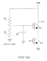
[0003] CMOS 트랜지스터들은 때때로, 신뢰성 목적을 위해 다수의 디바이스들에 걸쳐 전압 스윙을 분할하기 위해 적층된다. 도 1은 통상적인 증폭기 스테이지를 예시한다. 입력 신호는 (예를 들어, CS(common source) 구성에서) 하단 MOS 디바이스(101)의 게이트에 인가된다. (CG(common gate) 구성에서) 상단 캐스코드 디바이스(102)는 흔히 서플라이(supply)와 접지 간의 저항 엘리먼트(예를 들어, 레지스터들(103 및 104)을 포함하는 레지스터 래더(ladder))를 이용하여 바이어싱된다. 캐스코드 디바이스는 바이어스 전압을 보유(hold)하는 게이트 커패시턴스(105)를 갖는다. 저항 엘리먼트를 이용하여 서플라이 전압으로부터 회로의 노드들을 바이어싱하기 위한 종래의 접근법들은, 서플라이 전압이 일정한(또는 거의 일정한) 값을 유지하는 경우 만족스럽다. 그러나 서플라이 전압이 변하는 애플리케이션들에서, 저항 및 커패시턴스는 회로의 동작을 악화시킬 수 있다. [0003] CMOS transistors are sometimes stacked to divide the voltage swing across multiple devices for reliability purposes. Figure 1 illustrates a typical amplifier stage. The input signal is applied to the gate of the bottom MOS device 101 (e.g., in a common source (CS) configuration). The upper cascode device 102 (in a common gate (CG) configuration) often uses a resistive element between the supply and ground (e.g., a resistor
[0004] 본 개시는 광대역 바이어스 회로들에 대한 회로들 및 방법들을 포함한다. 일 예시적인 실시예에서, 증폭기는 증폭기의 입력과 출력 간에 캐스코드 트랜지스터를 포함한다. 캐스코드 트랜지스터는 파워 서플라이와 제 1 노드 간의 레지스터, 제 1 노드와 기준 전압(예를 들어, 접지) 간의 레지스터 및 파워 서플라이와 제 1 노드 간의 커패시터를 포함하는 바이어스 회로로부터 바이어스를 수신한다. 파워 서플라이는 캐스코드 트랜지스터의 제어 단자에서의 커패시턴스에 바이어스 회로를 통해 커플링되는 변조된 파워 서플라이일 수 있다. 인덕터는 캐스코드 트랜지스터의 단자와 파워 서플라이 간에 구성된다. 인덕터는 변조된 파워 서플라이 신호로부터 출력을 격리한다. [0004] This disclosure includes circuits and methods for wideband bias circuits. In one exemplary embodiment, the amplifier includes a cascode transistor between the input and the output of the amplifier. The cascode transistor receives a bias from a bias circuit comprising a resistor between the power supply and the first node, a resistor between the first node and a reference voltage (e.g., ground), and a capacitor between the power supply and the first node. The power supply may be a modulated power supply coupled through a bias circuit to the capacitance at the control terminal of the cascode transistor. The inductor is configured between the terminal of the cascode transistor and the power supply. The inductor isolates the output from the modulated power supply signal.
[0005] 일 실시예에서, 본 개시는 증폭기 회로를 포함하며, 이 증폭기 회로는 제어 단자, 제 1 단자 및 제 2 단자를 갖는 제 1 트랜지스터 ― 상기 제어 단자는 입력 신호를 수신하도록 구성됨 ― ; 제어 단자, 제 1 단자 및 제 2 단자를 갖는 캐스코드 트랜지스터 ― 상기 캐스코드 트랜지스터의 제 2 단자는 제 1 트랜지스터의 제 1 단자에 커플링됨 ― ; 캐스코드 트랜지스터의 제 1 단자에 커플링되는 제 1 단자 및 변조된 파워 서플라이 단자에 커플링되는 제 2 단자를 갖는 인덕터; 변조된 파워 서플라이 단자에 커플링되는 제 1 단자 및 제 1 노드에 커플링되는 제 2 단자를 갖는 제 1 레지스터; 제 1 노드에 커플링되는 제 1 단자 및 기준 전압에 커플링되는 제 2 단자를 갖는 제 2 레지스터; 및 변조된 파워 서플라이 단자에 커플링되는 제 1 단자 및 제 1 노드에 커플링되는 제 2 단자를 갖는 커패시터를 포함하고, 제 1 노드는 캐스코드 트랜지스터의 제어 단자에 커플링되고, 변조된 파워 서플라이 단자는 입력 신호에 대응하는 시변(time varying) 파워 서플라이 신호를 생성한다. [0005] In one embodiment, the present disclosure includes an amplifier circuit comprising a first transistor having a control terminal, a first terminal and a second terminal, the control terminal configured to receive an input signal; A cascode transistor having a control terminal, a first terminal and a second terminal, the second terminal of the cascode transistor being coupled to a first terminal of the first transistor; An inductor having a first terminal coupled to a first terminal of the cascode transistor and a second terminal coupled to the modulated power supply terminal; A first resistor having a first terminal coupled to the modulated power supply terminal and a second terminal coupled to the first node; A second resistor having a first terminal coupled to the first node and a second terminal coupled to the reference voltage; And a capacitor having a first terminal coupled to the modulated power supply terminal and a second terminal coupled to the first node, wherein the first node is coupled to the control terminal of the cascode transistor, and the modulated power supply Terminal generates a time varying power supply signal corresponding to the input signal.
[0006] 일 실시예에서, 캐스코드 트랜지스터의 제어 단자는 커패시턴스를 포함한다. [0006] In one embodiment, the control terminal of the cascode transistor comprises a capacitance.
[0007] 일 실시예에서, 제 1 레지스터, 제 2 레지스터, 및 커패시터는, 입력 신호의 제 2 주파수들 범위 보다 더 큰 제 1 주파수들 범위에 걸쳐서 캐스코드 디바이스의 제어 단자에 시변 파워 서플라이 신호를 커플링하도록 구성된다. [0007] In one embodiment, the first resistor, the second resistor, and the capacitor are connected to the control terminal of the cascode device over a first frequency range that is greater than the second frequency range of the input signal, .
[0008] 일 실시예에서, 제 1 레지스터의 저항과 커패시터의 커패시턴스의 제 1 곱(product)은 제 2 레지스터의 저항과 캐스코드 트랜지스터의 제어 단자에서의 커패시턴스의 제 2 곱과 대략적으로 동일하다. [0008] In one embodiment, the first product of the resistance of the first resistor and the capacitance of the capacitor is approximately equal to the second product of the resistance of the second resistor and the capacitance at the control terminal of the cascode transistor.
[0009] 일 실시예에서, 캐스코드 트랜지스터는 제 1 캐스코드 트랜지스터이고, 증폭기 회로는, 제어 단자, 제 1 단자 및 제 2 단자를 갖는 제 2 캐스코드 트랜지스터 ― 상기 제 2 캐스코드 트랜지스터의 제 1 단자는 제 1 캐스코드 트랜지스터의 제 2 단자에 커플링되고, 제 2 캐스코드 트랜지스터의 제 2 단자는 제 1 트랜지스터의 제 1 단자에 커플링됨 ― ; 변조된 파워 서플라이 단자에 커플링되는 제 1 단자 및 제 2 노드에 커플링되는 제 2 단자를 갖는 제 3 레지스터; 제 2 노드에 커플링되는 제 1 단자 및 기준 전압에 커플링되는 제 2 단자를 갖는 제 4 레지스터; 및 변조된 파워 서플라이 단자에 커플링되는 제 1 단자 및 제 2 노드에 커플링되는 제 2 단자를 갖는 제 2 커패시터를 더 포함하고, 제 2 노드는 제 2 캐스코드 트랜지스터의 제어 단자에 커플링된다. [0009] In one embodiment, the cascode transistor is a first cascode transistor and the amplifier circuit comprises a second cascode transistor having a control terminal, a first terminal and a second terminal, the first of the second cascode transistors Terminal coupled to a second terminal of the first cascode transistor and a second terminal of the second cascode transistor coupled to a first terminal of the first transistor; A third resistor having a first terminal coupled to the modulated power supply terminal and a second terminal coupled to the second node; A fourth resistor having a first terminal coupled to a second node and a second terminal coupled to a reference voltage; And a second capacitor having a first terminal coupled to the modulated power supply terminal and a second terminal coupled to the second node, the second node coupled to a control terminal of the second cascode transistor .
[0010] 일 실시예에서, 회로는 제 1 노드와 캐스코드 트랜지스터의 제어 단자 간에 커플링되는 제 3 레지스터를 더 포함한다. [0010] In one embodiment, the circuit further comprises a third register coupled between the first node and a control terminal of the cascode transistor.
[0011] 일 실시예에서, 인덕터는 인덕터의 제 2 단자 상에서 시변 파워 서플라이 신호로부터 캐스코드 트랜지스터의 제 1 단자를 격리한다. [0011] In one embodiment, the inductor isolates the first terminal of the cascode transistor from the time varying power supply signal on the second terminal of the inductor.
[0012] 일 실시예에서, 입력 신호의 대역폭은 시변 파워 서플라이 신호의 대역폭 미만이다. [0012] In one embodiment, the bandwidth of the input signal is less than the bandwidth of the time-varying power supply signal.
[0013] 다른 실시예에서, 본 개시는 신호를 증폭하는 방법을 포함하며, 이 방법은 제 1 트랜지스터의 제어 단자 상에서 입력 신호를 수신하는 단계 ― 상기 제 1 트랜지스터는 제어 단자, 제 1 단자, 및 제 2 단자를 가짐 ― ; 캐스코드 트랜지스터의 제 2 단자 상에서 출력 신호를 생성하도록 제 1 트랜지스터를 통한 입력 신호와 캐스코드 트랜지스터를 커플링하는 단계 ― 상기 캐스코드 트랜지스터는 제어 단자, 제 1 단자, 및 제 2 단자를 갖고, 캐스코드 트랜지스터의 제 2 단자는 제 1 트랜지스터의 제 1 단자에 커플링됨 ― ; 바이어스 회로의 단자 상에서 변조된 파워 서플라이로부터 시변 파워 서플라이 전압을 수신하는 단계 ― 상기 바이어스 회로는 변조된 파워 서플라이 단자에 커플링되는 제 1 단자 및 제 1 노드에 커플링되는 제 2 단자를 갖는 제 1 레지스터, 제 1 노드에 커플링되는 제 1 단자 및 기준 전압에 커플링되는 제 2 단자를 갖는 제 2 레지스터 및 변조된 파워 서플라이 단자에 커플링되는 제 1 단자 및 제 1 노드에 커플링되는 제 2 단자를 갖는 커패시터를 포함하고, 제 1 노드는 캐스코드 트랜지스터의 제어 단자에 커플링됨 ― ; 시변 파워 서플라이 전압을 캐스코드 트랜지스터의 제어 단자에 커플링하는 단계; 및 시변 파워 서플라이 전압으로부터 캐스코드 트랜지스터의 제 1 단자를 격리하도록 캐스코드 트랜지스터의 제 1 단자에 커플링되는 제 1 단자 및 변조된 파워 서플라이 단자에 커플링되는 제 2 단자를 갖는 인덕터에서 임피던스를 생성하는 단계를 포함한다. [0013] In another embodiment, the disclosure includes a method of amplifying a signal, the method comprising: receiving an input signal on a control terminal of a first transistor, the first transistor having a control terminal, a first terminal, Having a second terminal; Coupling a cascode transistor with an input signal through a first transistor to produce an output signal on a second terminal of the cascode transistor, the cascode transistor having a control terminal, a first terminal, and a second terminal, A second terminal of the code transistor being coupled to a first terminal of the first transistor; Receiving a time-varying power supply voltage from a modulated power supply on a terminal of a bias circuit, the bias circuit having a first terminal coupled to the modulated power supply terminal and a second terminal coupled to the first node, A second resistor having a first terminal coupled to the first node and a second terminal coupled to the reference voltage and a second terminal coupled to the modulated power supply terminal and a second terminal coupled to the second node coupled to the first node, A first node coupled to a control terminal of the cascode transistor; Coupling a time varying power supply voltage to a control terminal of the cascode transistor; And an impedance in the inductor having a first terminal coupled to the first terminal of the cascode transistor and a second terminal coupled to the modulated power supply terminal to isolate the first terminal of the cascode transistor from the time varying power supply voltage .
[0014] 일 실시예에서, 제 1 레지스터, 제 2 레지스터 및 커패시터는, 입력 신호의 제 2 주파수들 범위보다 더 큰 제 1 주파수들 범위에 걸쳐서 캐스코드 디바이스의 제어 단자에 시변 파워 서플라이 신호를 커플링하도록 구성된다. [0014] In one embodiment, the first resistor, the second resistor, and the capacitor couple the time varying power supply signal to the control terminal of the cascode device over a first range of frequencies that is greater than the second frequencies range of the input signal. .
[0015] 일 실시예에서, 바이어스 회로는 제 1 바이어스 회로이고, 캐스코드 트랜지스터는 제 1 캐스코드 트랜지스터이고, 상기 방법은, 제 2 바이어스 회로의 단자 상에서 변조된 파워 서플라이로부터 시변 파워 서플라이 전압을 수신하는 단계 ― 상기 제 2 바이어스 회로는 변조된 파워 서플라이 단자에 커플링되는 제 1 단자 및 제 2 노드에 커플링되는 제 2 단자를 갖는 제 3 레지스터, 제 2 노드에 커플링되는 제 1 단자 및 기준 전압에 커플링되는 제 2 단자를 갖는 제 4 레지스터, 및 변조된 파워 서플라이 단자에 커플링되는 제 1 단자 및 제 2 노드에 커플링되는 제 2 단자를 갖는 제 2 커패시터를 포함하고, 제 2 노드는 제 2 캐스코드 트랜지스터의 제어 단자에 커플링됨 ― ; 및 시변 파워 서플라이 전압을 제 2 캐스코드 트랜지스터의 제어 단자에 커플링하는 단계를 더 포함한다. [0015] In one embodiment, the bias circuit is a first bias circuit, and the cascode transistor is a first cascode transistor, and the method includes receiving a time-varying power supply voltage from a power supply modulated on a terminal of the second bias circuit Wherein the second bias circuit comprises a third resistor having a first terminal coupled to the modulated power supply terminal and a second terminal coupled to the second node, a first terminal coupled to the second node, And a second capacitor having a first terminal coupled to the modulated power supply terminal and a second terminal coupled to the second node, the second capacitor having a second terminal coupled to the second node, Is coupled to a control terminal of a second cascode transistor; And coupling the time varying power supply voltage to the control terminal of the second cascode transistor.
[0016] 일 실시예에서, 이 방법은 제 1 노드와 캐스코드 트랜지스터의 제어 단자 간에 커플링되는 제 3 레지스터를 통해 시변 파워 서플라이 전압을 커플링하는 단계를 더 포함한다. [0016] In one embodiment, the method further comprises coupling a time-varying power supply voltage through a third resistor coupled between the first node and a control terminal of the cascode transistor.
[0017] 다른 실시예에서, 본 개시는 증폭기 회로를 포함하며, 이 증폭기 회로는, 제어 단자, 제 1 단자 및 제 2 단자를 갖는 제 1 트랜지스터 ― 상기 제어 단자는 입력 신호를 수신하도록 구성됨 ― ; 제어 단자, 제 1 단자 및 제 2 단자를 갖는 캐스코드 트랜지스터 ― 상기 제 2 단자는 제 1 트랜지스터의 제 1 단자에 커플링됨 ― ; 캐스코드 트랜지스터의 제 1 단자에 커플링되는 제 1 단자 및 변조된 파워 서플라이 단자를 수신하도록 커플링되는 제 2 단자를 갖는 인덕터; 캐스코드 트랜지스터를 바이어싱하기 위해 변조된 파워 서플라이 단자로부터의 입력 신호에 대응하는 시변 파워 서플라이 신호의 최대 주파수를 캐스코드 트랜지스터의 제어 단자에 커플링하기 위한 수단을 포함한다. [0017] In another embodiment, the present disclosure includes an amplifier circuit comprising: a first transistor having a control terminal, a first terminal and a second terminal, the control terminal configured to receive an input signal; A cascode transistor having a control terminal, a first terminal and a second terminal, the second terminal coupled to a first terminal of the first transistor; An inductor having a first terminal coupled to a first terminal of the cascode transistor and a second terminal coupled to receive a modulated power supply terminal; And means for coupling the maximum frequency of the time-varying power supply signal corresponding to the input signal from the modulated power supply terminal to the control terminal of the cascode transistor for biasing the cascode transistor.
[0018] 일 실시예에서, 시변 파워 서플라이 신호의 최대 주파수를 커플링하기 위한 수단은, 변조된 파워 서플라이 단자에 커플링되는 제 1 단자 및 캐스코드 트랜지스터의 제어 단자에 커플링되는 제 2 단자를 갖는 제 1 레지스터; 캐스코드 트랜지스터의 제어 단자에 커플링되는 제 1 단자 및 기준 전압에 커플링되는 제 2 단자를 갖는 제 2 레지스터; 변조된 파워 서플라이 단자에 커플링되는 제 1 단자 및 캐스코드 트랜지스터의 제어 단자에 커플링되는 제 2 단자를 갖는 커패시터; 및 캐스코드 트랜지스터의 제어 단자에 커플링되는 커패시턴스를 포함한다. [0018] In one embodiment, the means for coupling the maximum frequency of the time-varying power supply signal comprises a first terminal coupled to the modulated power supply terminal and a second terminal coupled to the control terminal of the cascode transistor A first register having a first register; A second resistor having a first terminal coupled to a control terminal of the cascode transistor and a second terminal coupled to a reference voltage; A capacitor having a first terminal coupled to the modulated power supply terminal and a second terminal coupled to a control terminal of the cascode transistor; And a capacitance coupled to a control terminal of the cascode transistor.
[0019] 일 실시예에서, 시변 파워 서플라이 신호의 최대 주파수를 커플링하기 위한 수단은, 변조된 파워 서플라이 단자에 커플링되는 제 1 단자 및 제 1 노드에 커플링되는 제 2 단자를 갖는 제 1 레지스터; 제 1 노드에 커플링되는 제 1 단자 및 기준 전압에 커플링되는 제 2 단자를 갖는 제 2 레지스터; 변조된 파워 서플라이 단자에 커플링되는 제 1 단자 및 제 1 노드에 커플링되는 제 2 단자를 갖는 커패시터; 제 1 노드와 캐스코드 트랜지스터의 제어 단자 간에 커플링되는 제 3 레지스터; 및 캐스코드 트랜지스터의 제어 단자에 커플링되는 커패시턴스를 포함한다. [0019] In one embodiment, the means for coupling the maximum frequency of the time-varying power supply signal comprises a first terminal coupled to the modulated power supply terminal and a second terminal coupled to the first node, register; A second resistor having a first terminal coupled to the first node and a second terminal coupled to the reference voltage; A capacitor having a first terminal coupled to the modulated power supply terminal and a second terminal coupled to the first node; A third register coupled between the first node and the control terminal of the cascode transistor; And a capacitance coupled to a control terminal of the cascode transistor.
[0020] 이어지는 상세한 설명 및 첨부 도면들은 본 개시의 성질 및 이점들의 더 나은 이해를 제공한다. [0020] The following detailed description and the annexed drawings provide a better understanding of the nature and advantages of the present disclosure.
[0021] 도 1은 저항성 및 용량성 엘리먼트들을 포함하는 종래의 바이어스 회로를 예시한다.
[0022] 도 2a는 일 실시예에 따른 예시적인 광대역 바이어스 회로를 예시한다.
[0023] 도 2b는 다른 실시예에 따른 예시적인 광대역 바이어스 회로를 예시한다.
[0024] 도 3a는 일 실시예에 따른 증폭기 회로의 예시적인 광대역 바이어스 회로를 예시한다 .
[0025] 도 3b는 도 3a의 예시적인 광대역 바이어스 회로의 주파수 응답을 예시한다.
[0026] 도 4는 다른 실시예에 따른 광대역 바이어스 회로의 다른 예를 예시한다.
[0027] 도 5는 다른 실시예에 따른 광대역 바이어스 회로들의 다른 예를 예시한다.
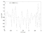
[0028] 도 6은 일 실시예에 따른 엔벨로프 및 입력 신호의 예시적인 스펙트럼을 예시한다.
[0029] 도 7a는 일 실시예에 따른 예시적인 신호를 예시한다.
[0030] 도 7b는 일 실시예에 따른 예시적인 엔벨로프를 예시한다. [0021] FIG. 1 illustrates a conventional bias circuit including resistive and capacitive elements.
[0022] FIG. 2A illustrates an exemplary wideband bias circuit in accordance with one embodiment.
[0023] FIG. 2B illustrates an exemplary wideband bias circuit according to another embodiment.
[0024] FIG. 3a illustrates an exemplary broadband bias circuit of an amplifier circuit in accordance with one embodiment.
[0025] FIG. 3B illustrates the frequency response of the exemplary wideband bias circuit of FIG. 3A.
[0026] FIG. 4 illustrates another example of a broadband bias circuit according to another embodiment.
[0027] FIG. 5 illustrates another example of wideband bias circuits according to another embodiment.
[0028] FIG. 6 illustrates an exemplary spectrum of an envelope and input signal in accordance with one embodiment.
[0029] FIG. 7A illustrates an exemplary signal according to one embodiment.
[0030] FIG. 7b illustrates an exemplary envelope in accordance with one embodiment.
[0031] 본 개시는 광대역 바이어스 회로들에 관한 것이다. 이어지는 설명에서, 설명을 위해, 다수의 예들 및 특정 세부사항들이 본 개시의 철저한 이해를 제공하기 위해 기술된다. 그러나 청구범위에서 표현된 바와 같은 본 개시는, 아래에서 설명되는 다른 특징들과 결합하여, 또는 단독으로 이러한 예들의 특징들 중 일부만 또는 전부를 포함할 수 있고, 여기서 설명된 특징들 및 개념들의 변형들 및 등가물들을 더 포함할 수 있다는 것이 당업자에게 자명하게 될 것이다. [0031] The present disclosure relates to broadband bias circuits. In the following description, for purposes of explanation, numerous examples and specific details are set forth in order to provide a thorough understanding of the present disclosure. It is to be understood, however, that this disclosure, as expressed in the claims, may include some or all of the features of these examples in combination with other features described below, or alone, and variations of the features and concepts described herein It will be apparent to those skilled in the art that various modifications, additions, substitutions, and equivalents may be resorted to.
[0032] 본 개시의 몇몇 실시예들은 엔벨로프 트래킹(envelope tracking) 애플리케이션들에 관한 것이다. 엔벨로프 트래킹 애플리케이션에서, 파워 서플라이 전압(Vdd)은 회로의 전력 소비를 감소시키기 위해 시간에 걸쳐 변동될 수 있다. 시변(time varying) 파워 서플라이 전압은 입력 신호가 더 적은 전력을 이용하여 프로세싱될 수 있도록 입력 신호에 대응할 수 있다. ET(envelope tracking)을 이용한 일 예시적인 시스템은 무선 시스템의 전력 증폭기(예를 들어, 신호들을 안테나로 유도하는 전송 경로의 전력 증폭기)이다. [0032] Some embodiments of the present disclosure relate to envelope tracking applications. In an envelope tracking application, the power supply voltage (Vdd) may vary over time to reduce the power consumption of the circuit. The time varying power supply voltage may correspond to the input signal so that the input signal can be processed using less power. One exemplary system using envelope tracking (ET) is a power amplifier in a wireless system (e.g., a power amplifier in a transmission path leading signals to an antenna).
[0033] 몇몇 ET 애플리케이션들에서, 엔벨로프 신호의 대역폭은 프로세싱되는 신호의 대역폭보다 상당히 더 높을 수 있다. 예를 들어, 전력 증폭기 서플라이 전압(VDD_ET)은 전송되는 신호의 대역폭의 5-10배까지 확장될 수 있는 엔벨로프 주파수들에서 변조될 수 있다. 예를 들어, 20MHz의 LTE(long term evolution) 무선 프로토콜에서, 파워 서플라이의 대역폭은 200MHz까지 확장될 수 있다. [0033] In some ET applications, the bandwidth of the envelope signal may be significantly higher than the bandwidth of the signal being processed. For example, the power amplifier supply voltage (VDD_ET) can be modulated at the envelope frequencies that can be extended to 5-10 times the bandwidth of the transmitted signal. For example, in a long term evolution (LTE) wireless protocol of 20 MHz, the bandwidth of the power supply can be extended to 200 MHz.
[0034] 도 1에서 도시된 바와 같은 종래 기술의 바이어스 회로들의 바이어스 레지스터들과 게이트 커패시턴스의 결합은 저역 통과 주파수 응답을 생성한다. 게이트 커패시턴스의 공통 값들에 대해, 레지스터들은 바람직한 대역폭을 달성하도록 매우 작을(수백 옴 범위) 필요가 있을 것이지만, 매우 큰 PAE(power amplifier efficiency) 저감(degradation)(통상적인 UMTS(Universal Mobile Telecommunications System) 최대 전력 조건들에 대해 대략 3-5%)을 초래한다. [0034] The combination of the bias resistors and the gate capacitance of the prior art bias circuits as shown in Figure 1 produces a low pass frequency response. For common values of gate capacitance, the resistors will need to be very small (in the hundreds of ohms) to achieve the desired bandwidth, but very large power amplifier efficiency (PAE) degradation (typical Universal Mobile Telecommunications System (UMTS) About 3-5% for power conditions).
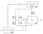
[0035] 도 2a는 일 실시예에 따른 예시적인 광대역 바이어스 회로를 예시한다. 이 예에서, 회로(210)는 입력 신호(IN)를 수신할 수 있고 출력 신호(OUT)를 생성할 수 있다. 출력 신호(OUT)는 예를 들어, 공중파(airwave)를 통한 전송을 위해 안테나(도시되지 않음)에 커플링되는 RF 신호일 수 있다. 회로(210)는 특정한 값들로 바이어싱되는 하나 또는 그 초과의 내부 노드들을 포함할 수 있다. 이 예에서, 회로(210)는 변조된 파워 서플라이(230)로부터 시간에 걸쳐 변동될 수 있는 파워 서플라이 전압(VDD_ET)을 수신할 수 있다. 예를 들어, 몇몇 애플리케이션들에서, 사전프로세싱 블록(240)은 전송될 신호(S)를 수신하고, 예를 들어, 엔벨로프 트래킹을 제어하기 위해 입력 신호(IN) 및 변조 제어 신호(Se)를 생성할 수 있다. 예를 들어, 회로(210)는 시변 파워 서플라이(VDD_ET)를 이용하여 ET(envelope tracking)을 수행할 수 있다. 본 개시의 특징들 및 이점들은 VDD에 따라 변동되는, 회로 노드에 대한 바이어스를 생성할 수 있는 광대역 바이어스 회로를 포함한다. 출력(OUT)은 예를 들어, 출력 신호로부터 바이어스 회로를 또한 격리할 수 있는 인덕터(L1)(220)를 이용하여 파워 서플라이 신호로부터 격리될 수 있다. 회로 노드는 입력 신호의 신호 경로에서 회로에 바이어스 전압을 제공할 수 있고, 이에 따라 예를 들어, 전력 소비를 감소시키도록 시변 파워 서플라이 전압을 이용하여 바이어싱될 수 있다. 이 예에서, 커패시터(C1)(203)는 하단 레지스터 래더 레지스터(R2)(202) 및 커패시턴스(C2)(204)에 의해 설정된 기존의 폴(pole)로 제로-폴 상쇄(zero-pole cancellation)를 수행하기 위해 레지스터 래더의 상단 레지스터(R1)(201)와 병렬로 부가되어, 상당한 대역폭 확장을 발생시킨다. 커패시턴스(C2)(204)는 예를 들어, 트랜지스터 바이어스 노드에서의 총 커패시턴스일 수 있고, 고유한 디바이스 커패시턴스, 노드에 부가된 임의의 추가의 커패시턴스(예를 들어, MIM 또는 MOS 커패시턴스들)는 물론 기생 커패시턴스들을 포함할 수 있다. 커패시터(C1)의 부가는, 레지스터들(R1 및 R2)의 상당히 더 큰 값들의 이용을 허용하며, 이는 예를 들어, 더 높은 PAE를 발생시킬 수 있다. C1은 바이어스 회로에 부가될 수 있고, 아래와 같이 레지스터들 및 커패시터들의 값들을 세팅함으로써, 다음의 전달 함수가 VDD_ET와 바이어스 노드 사이에서 달성될 수 있다:[0035] FIG. 2A illustrates an exemplary wideband bias circuit in accordance with one embodiment. In this example, the
![]()
![]()
이에 따라, 시변 파워 서플라이 전압(예를 들어, 엔벨로프 신호)은 예를 들어, 파워 서플라이 신호로부터의 고주파수들을 과도하게 제거함 없이, 노드를 바이어싱하기 위해 회로의 바이어스 노드에 커플링될 수 있다. 일 실시예에서, 커패시턴스들 또는 저항들 중 하나 또는 그 초과는 프로그래밍 가능할 수 있다. 프로그래밍 및 튜닝의 부가는 예를 들어, 회로 대역폭 및 바이어스 전압의 독립적인 제어를 허용할 수 있다. Thus, the time varying power supply voltage (e. G., The envelope signal) can be coupled to the bias node of the circuit to bias the node, for example, without excessively removing high frequencies from the power supply signal. In one embodiment, one or more of the capacitances or resistors may be programmable. The addition of programming and tuning may allow independent control of, for example, circuit bandwidth and bias voltage.
[0036] 도 2b는 다른 실시예에 따른 예시적인 광대역 바이어스 회로를 예시한다. 이 예에서, 레지스터(R3)(205)는 R1, R2, 및 C1의 단자들과 기생 노드 커패시턴스(C2)를 포함하는 바이어스 노드 간에 구성된다. 이 예시적인 구성은 특정한 주파수들(예를 들어, RF 주파수들)에서 로딩을 감소시킬 수 있지만, 회로의 고주파수 대역폭을 제한할 수 있다. 다음의 전달 함수는 도 2b에서 도시된 구성을 이용하여 바이어스 노드와 VDD_ET 간에 달성될 수 있다:[0036] FIG. 2B illustrates an exemplary wideband bias circuit according to another embodiment. In this example, the register (R3) 205 is configured between the terminals of R1, R2, and C1 and the bias node including the parasitic node capacitance C2. This exemplary configuration can reduce loading at specific frequencies (e.g., RF frequencies), but can limit the high frequency bandwidth of the circuit. The following transfer function can be achieved between the bias node and VDD_ET using the configuration shown in Figure 2B:
![]()
![]()
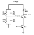
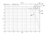
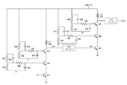
[0037] 도 3a는 일 실시예에 따른 증폭기 회로의 예시적인 광대역 바이어스 회로를 예시한다. 이 예는 증폭기 회로에서 캐스코드 트랜지스터(311)의 게이트 상에서 바이어스 전압을 생성하기 위한 광대역 바이어스 회로의 애플리케이션을 예시한다. 이 예에서, 입력 신호(IN)는 NMOS 트랜지스터(312)의 게이트 상에서 수신된다. 트랜지스터(312)는 트랜지스터(311)의 소스에 커플링된 드레인을 갖는다. 트랜지스터(311)의 드레인은 인덕터(L1)(310)를 통해 시변 파워 서플라이 전압(VDD_ET)에 커플링된다. 출력 신호(OUT)는 인덕터(L1)의 단자와 트랜지스터(311)의 드레인 상에서 생성된다. VDD_ET는 예를 들어, 엔벨로프 트래킹을 구현할 수 있다. 변조된 파워 서플라이 전압은 레지스터(R1)(301), 레지스터(R2)(302), 커패시터(C1)(303) 및 게이트 커패시턴스(C2)(304)를 포함하는 광대역 바이어스 회로에 의해 트랜지스터(311)의 게이트에서 적절한 바이어스 전압으로 변환된다. 예를 들어, 인덕터(310)는 파워 서플라이 신호로부터 트랜지스터(311)의 드레인의 출력을 격리하고, 출력 신호로부터 바이어스 회로를 격리할 수 있다. 도 3b는 도 3a의 예시적인 광대역 바이어스 회로의 주파수 응답을 예시한다. 응답(350)은, 커패시터(C1)가 없는 경우의 응답이 고주파수들에서 강하하는 것을 예시한다. 응답들(351-355)은, C1의 상이한 값들에 대한 응답들이 더 높은 주파수에서 대략 일정(flat)하게 유지되며 급락하지 않는다는 것을 예시한다. [0037] FIG. 3A illustrates an exemplary wideband bias circuit of an amplifier circuit in accordance with one embodiment. This example illustrates the application of a broadband bias circuit for generating a bias voltage on the gate of the
[0038] 도 4는 다른 실시예에 따른 광대역 바이어스 회로의 다른 예를 예시한다. 이 예는 일 실시예에 따라 광대역 바이어스 회로들을 포함하는 구동기 증폭기 및 전력 증폭기를 예시한다. 구동기 증폭기는, 캐스코드 구성으로 배열되고 인덕터(L1)(413)를 통해 파워 서플라이에 커플링되는 NMOS 트랜지스터들(410-412)을 포함한다. 입력 신호(IN1)는 트랜지스터(410)의 게이트 상에서 수신되고, 입력 신호에 대응하는 시변 파워 서플라이 전압(VDD-ET)은 파워 서플라이 단자에서 수신된다. 레지스터들(401-402) 및 커패시터들(403-404)을 포함하는 제 1 광대역 바이어스 회로는 트랜지스터(411)의 게이트 상에서 바이어스 전압을 생성하며, 여기서 커패시턴스(404)는 트랜지스터(411)의 게이트 커패시턴스(예를 들어, 디바이스 커패시턴스, 부가적인 부가된 커패시턴스 및 기생 커패시턴스)를 포함한다. 레지스터들(405-406) 및 커패시터들(407-408)을 포함하는 제 2 광대역 바이어스 회로는 트랜지스터(412)의 게이트 상에서 바이어스 전압을 생성하며, 여기서 커패시턴스(408)는 또한 트랜지스터(412)의 게이트 커패시턴스를 포함한다. 구동기 회로의 출력 신호(OUT1)는 트랜지스터(412)의 드레인과 L1 간의 노드로부터 도래한다. OUT1은 예를 들어, 매칭 네트워크(490)를 통해 전력 증폭기의 입력에 제공된다. [0038] FIG. 4 illustrates another example of a broadband bias circuit according to another embodiment. This example illustrates a driver amplifier and a power amplifier comprising broadband bias circuits in accordance with one embodiment. The driver amplifier includes NMOS transistors 410-412 that are arranged in a cascode configuration and coupled to the power supply via inductor (L1) 413. The input signal IN1 is received on the gate of the
[0039] 유사하게, 전력 증폭기는, 인덕터 L2(433)를 통해 파워 서플라이에 커플링되고 캐스코드 구성으로 배열되는 NMOS 트랜지스터들(430-432)을 포함한다. 입력 신호(IN2)는 매칭 네트워크(490)로부터 트랜지스터(430)의 게이트 상에서 수신되며, 입력 신호에 대응하는 시변 파워 서플라이 전압(VDD-ET)은 파워 서플라이 단자에서 수신된다. 레지스터들(421-422) 및 커패시터들(423-424)을 포함하는 제 3 광대역 바이어스 회로는 트랜지스터(431)의 게이트 상에서 바이어스 전압을 생성하며, 여기서 커패시턴스(424)는 트랜지스터(431)의 게이트 커패시턴스(예를 들어, 디바이스 커패시턴스, 부가적인 부가된 커패시턴스 및 기생 커패시턴스)를 포함한다. 레지스터들(425-426) 및 커패시터들(427-428)을 포함하는 제 4 광대역 바이어스 회로는 트랜지스터(432)의 게이트 상에서 바이어스 전압을 생성하며, 여기서 커패시턴스(428)는 또한 트랜지스터(432)의 게이트 커패시턴스를 포함한다. 전력 증폭기의 출력 신호는 트랜지스터(432)의 드레인과 L2 간의 노드로부터 도래한다. 출력 신호(OUT2)는 예를 들어, 매칭 네트워크(491)를 통해 안테나에 제공된다.[0039] Similarly, the power amplifier includes NMOS transistors 430-432 coupled to the power supply through
[0040] 도 5는 다른 실시예에 따른 광대역 바이어스 회로들의 다른 예를 예시한다. 이 예는, 각각의 광대역 바이어스 회로가 광대역 바이어스 회로의 다른 엘리먼트들과 각각의 캐스코드 트랜지스터의 게이트 커패시턴스 간에 레지스터를 포함한다는 것을 제외하면, 도 4에서 도시된 것과 동일하다. [0040] FIG. 5 illustrates another example of wideband bias circuits according to another embodiment. This example is the same as that shown in Figure 4, except that each wideband bias circuit includes a resistor between the other elements of the broadband bias circuit and the gate capacitance of each cascode transistor.
[0041] 도 6은 일 실시예에 따른 엔벨로프 및 입력 신호의 예시적인 스펙트럼을 예시한다. 이 예는, 시변 파워 서플라이 전압의 주파수 범위가 예를 들어, 증폭되는 입력 신호의 주파수 범위보다 더 클 수 있다는 것을 예시한다. 도 6에서 도시된 예는, LTE 신호 및 LTE 엔벨로프를 예시한다. 도 7a는 일 실시예에 따른 예시적인 신호를 예시한다. 도 7a는 입력 신호의 동위상 및 직교 위상의 컴포넌트들 모두를 도시한다. 도 7b는 일 실시예에 따른 예시적인 엔벨로프를 예시한다. 도 7b는 도 7a의 입력 신호에 대한 신호 엔벨로프를 도시한다. [0041] FIG. 6 illustrates an exemplary spectrum of an envelope and input signal in accordance with one embodiment. This example illustrates that the frequency range of the time varying power supply voltage may be greater than the frequency range of the input signal to be amplified, for example. The example shown in FIG. 6 illustrates an LTE signal and an LTE envelope. 7A illustrates an exemplary signal according to one embodiment. Figure 7A shows both the in-phase and quadrature components of the input signal. 7B illustrates an exemplary envelope in accordance with one embodiment. Figure 7b shows the signal envelope for the input signal of Figure 7a.
[0042] 위의 설명은 특정한 실시예들의 양상들이 어떻게 구현되는지에 관한 예와 함께 본 개시의 다양한 실시예들을 예시한다. 예를 들어, 위의 예들이 NMOS 트랜지스터들의 견지에서 설명되지만, 다른 트랜지스터 타입들이 또한 이용될 수 있다. 위의 예들은 유일한 실시예들로 고려되어선 안 되고, 다음의 청구항들에 의해 정의된 바와 같은 특정한 실시예들의 이점들 및 유연성을 예시하도록 제시된다. 위의 개시 및 이어지는 청구항들에 기초하여, 다른 어레인지먼트들, 실시예들, 구현들 및 등가물들이 청구항들에 의해 정의된 바와 같은 본 개시의 범위로부터 벗어남 없이 이용될 수 있다. [0042] The foregoing description illustrates various embodiments of the present disclosure, with examples of how aspects of certain embodiments may be implemented. For example, while the above examples are described in terms of NMOS transistors, other transistor types may also be used. The above examples are not to be considered as unique embodiments, but are presented to illustrate the advantages and flexibility of certain embodiments as defined by the following claims. Other arrangements, embodiments, implementations and equivalents may be utilized without departing from the scope of the present disclosure as defined by the claims, based on the foregoing disclosure and the following claims.
Claims (20)
제어 단자, 제 1 단자 및 제 2 단자를 갖는 제 1 트랜지스터 ― 상기 제어 단자는 입력 신호를 수신하도록 구성됨 ― ;
제어 단자, 제 1 단자 및 제 2 단자를 갖는 캐스코드 트랜지스터 ― 상기 캐스코드 트랜지스터의 제 2 단자는 상기 제 1 트랜지스터의 제 1 단자에 커플링됨 ― ;
상기 캐스코드 트랜지스터의 제 1 단자에 커플링되는 제 1 단자 및 변조된 파워 서플라이 단자에 커플링되는 제 2 단자를 갖는 인덕터;
상기 변조된 파워 서플라이 단자에 커플링되는 제 1 단자 및 제 1 노드에 커플링되는 제 2 단자를 갖는 제 1 레지스터;
상기 제 1 노드에 커플링되는 제 1 단자 및 기준 전압에 커플링되는 제 2 단자를 갖는 제 2 레지스터; 및
상기 변조된 파워 서플라이 단자에 커플링되는 제 1 단자 및 상기 제 1 노드에 커플링되는 제 2 단자를 갖는 커패시터
를 포함하고,
상기 제 1 노드는 상기 캐스코드 트랜지스터의 제어 단자에 커플링되고, 상기 변조된 파워 서플라이 단자는 상기 입력 신호에 대응하는 시변(time varying) 파워 서플라이 신호를 생성하는,
증폭기 회로.As an amplifier circuit,
A first transistor having a control terminal, a first terminal and a second terminal, the control terminal configured to receive an input signal;
A cascode transistor having a control terminal, a first terminal and a second terminal, the second terminal of the cascode transistor being coupled to a first terminal of the first transistor;
An inductor having a first terminal coupled to the first terminal of the cascode transistor and a second terminal coupled to the modulated power supply terminal;
A first resistor having a first terminal coupled to the modulated power supply terminal and a second terminal coupled to the first node;
A second resistor having a first terminal coupled to the first node and a second terminal coupled to a reference voltage; And
A capacitor having a first terminal coupled to the modulated power supply terminal and a second terminal coupled to the first node,
Lt; / RTI >
Wherein the first node is coupled to a control terminal of the cascode transistor and the modulated power supply terminal generates a time varying power supply signal corresponding to the input signal,
Amplifier circuit.
상기 캐스코드 트랜지스터의 제어 단자는 커패시턴스를 포함하는,
증폭기 회로.The method according to claim 1,
Wherein the control terminal of the cascode transistor comprises a capacitance,
Amplifier circuit.
상기 제 1 레지스터, 상기 제 2 레지스터, 및 상기 커패시터는, 상기 입력 신호의 제 2 주파수들 범위보다 더 큰 제 1 주파수들 범위에 걸쳐서 캐스코드 트랜지스터의 제어 단자에 상기 시변 파워 서플라이 신호를 커플링하도록 구성되는,
증폭기 회로.3. The method of claim 2,
The first resistor, the second resistor, and the capacitor are coupled to the control terminal of the cascode transistor over a range of first frequencies that is greater than a second frequency range of the input signal to couple the time varying power supply signal Configured,
Amplifier circuit.
상기 제 1 레지스터의 저항과 상기 커패시터의 커패시턴스의 제 1 곱(product)은 상기 제 2 레지스터의 저항과 상기 캐스코드 트랜지스터의 제어 단자에서의 커패시턴스의 제 2 곱과 대략적으로 동일한,
증폭기 회로.The method according to claim 1,
Wherein a first product of a resistance of the first resistor and a capacitance of the capacitor is approximately equal to a second product of a resistance of the second resistor and a capacitance at a control terminal of the cascode transistor,
Amplifier circuit.
상기 캐스코드 트랜지스터는 제 1 캐스코드 트랜지스터이고,
상기 증폭기 회로는,
제어 단자, 제 1 단자 및 제 2 단자를 갖는 제 2 캐스코드 트랜지스터 ― 상기 제 2 캐스코드 트랜지스터의 제 1 단자는 상기 제 1 캐스코드 트랜지스터의 제 2 단자에 커플링되고, 상기 제 2 캐스코드 트랜지스터의 제 2 단자는 상기 제 1 트랜지스터의 제 1 단자에 커플링됨 ― ;
상기 변조된 파워 서플라이 단자에 커플링되는 제 1 단자 및 제 2 노드에 커플링되는 제 2 단자를 갖는 제 3 레지스터;
상기 제 2 노드에 커플링되는 제 1 단자 및 상기 기준 전압에 커플링되는 제 2 단자를 갖는 제 4 레지스터; 및
상기 변조된 파워 서플라이 단자에 커플링되는 제 1 단자 및 상기 제 2 노드에 커플링되는 제 2 단자를 갖는 제 2 커패시터
를 더 포함하고,
상기 제 2 노드는 상기 제 2 캐스코드 트랜지스터의 제어 단자에 커플링되는,
증폭기 회로.The method according to claim 1,
Wherein the cascode transistor is a first cascode transistor,
The amplifier circuit comprising:
A second cascode transistor having a control terminal, a first terminal and a second terminal, the first terminal of the second cascode transistor being coupled to a second terminal of the first cascode transistor, A second terminal of the first transistor coupled to a first terminal of the first transistor;
A third resistor having a first terminal coupled to the modulated power supply terminal and a second terminal coupled to a second node;
A fourth resistor having a first terminal coupled to the second node and a second terminal coupled to the reference voltage; And
A second capacitor having a first terminal coupled to the modulated power supply terminal and a second terminal coupled to the second node,
Further comprising:
Said second node coupled to a control terminal of said second cascode transistor,
Amplifier circuit.
상기 제 1 노드와 상기 캐스코드 트랜지스터의 제어 단자 간에 커플링되는 제 3 레지스터
를 더 포함하는,
증폭기 회로.The method according to claim 1,
A third register coupled between the first node and a control terminal of the cascode transistor;
≪ / RTI >
Amplifier circuit.
상기 인덕터는 상기 인덕터의 제 2 단자 상에서 상기 시변 파워 서플라이 신호로부터 상기 캐스코드 트랜지스터의 제 1 단자를 격리하는,
증폭기 회로.The method according to claim 1,
The inductor isolating the first terminal of the cascode transistor from the time varying power supply signal on a second terminal of the inductor,
Amplifier circuit.
상기 입력 신호의 대역폭은 상기 시변 파워 서플라이 신호의 대역폭 미만인,
증폭기 회로.The method according to claim 1,
Wherein the bandwidth of the input signal is less than the bandwidth of the time-varying power supply signal,
Amplifier circuit.
상기 제 1 레지스터, 상기 제 2 레지스터 및 상기 커패시터 중 적어도 하나는 프로그래밍 가능한,
증폭기 회로.The method according to claim 1,
Wherein at least one of the first register, the second register, and the capacitor is programmable,
Amplifier circuit.
제 1 트랜지스터의 제어 단자 상에서 입력 신호를 수신하는 단계 ― 상기 제 1 트랜지스터는 제어 단자, 제 1 단자, 및 제 2 단자를 가짐 ― ;
캐스코드 트랜지스터의 제 2 단자 상에서 출력 신호를 생성하도록 상기 제 1 트랜지스터를 통한 입력 신호와 상기 캐스코드 트랜지스터를 커플링하는 단계 ― 상기 캐스코드 트랜지스터는 제어 단자, 제 1 단자, 및 제 2 단자를 갖고, 상기 캐스코드 트랜지스터의 제 2 단자는 상기 제 1 트랜지스터의 제 1 단자에 커플링됨 ― ;
바이어스 회로의 단자 상에서 변조된 파워 서플라이로부터 시변 파워 서플라이 전압을 수신하는 단계 ― 상기 바이어스 회로는 변조된 파워 서플라이 단자에 커플링되는 제 1 단자 및 제 1 노드에 커플링되는 제 2 단자를 갖는 제 1 레지스터, 상기 제 1 노드에 커플링되는 제 1 단자 및 기준 전압에 커플링되는 제 2 단자를 갖는 제 2 레지스터 및 상기 변조된 파워 서플라이 단자에 커플링되는 제 1 단자 및 상기 제 1 노드에 커플링되는 제 2 단자를 갖는 커패시터를 포함하고, 상기 제 1 노드는 상기 캐스코드 트랜지스터의 제어 단자에 커플링됨 ― ;
상기 시변 파워 서플라이 전압을 상기 캐스코드 트랜지스터의 제어 단자에 커플링하는 단계; 및
상기 시변 파워 서플라이 전압으로부터 상기 캐스코드 트랜지스터의 제 1 단자를 격리하도록 상기 캐스코드 트랜지스터의 제 1 단자에 커플링되는 제 1 단자 및 변조된 파워 서플라이 단자에 커플링되는 제 2 단자를 갖는 인덕터에서 임피던스를 생성하는 단계
를 포함하는,
신호를 증폭하는 방법.CLAIMS 1. A method for amplifying a signal,
Receiving an input signal on a control terminal of a first transistor, the first transistor having a control terminal, a first terminal, and a second terminal;
Coupling a cascode transistor with an input signal through the first transistor to produce an output signal on a second terminal of the cascode transistor, the cascode transistor having a control terminal, a first terminal, and a second terminal A second terminal of the cascode transistor coupled to a first terminal of the first transistor;
Receiving a time-varying power supply voltage from a modulated power supply on a terminal of a bias circuit, the bias circuit having a first terminal coupled to the modulated power supply terminal and a first terminal coupled to the first node, A second resistor having a first terminal coupled to the first node and a second terminal coupled to a reference voltage, a first terminal coupled to the modulated power supply terminal, and a second terminal coupled to the first node, A first node coupled to a control terminal of the cascode transistor;
Coupling the time varying power supply voltage to a control terminal of the cascode transistor; And
An inductor having a first terminal coupled to a first terminal of the cascode transistor to isolate a first terminal of the cascode transistor from the time varying power supply voltage and a second terminal coupled to the modulated power supply terminal, ≪ / RTI >
/ RTI >
A method for amplifying a signal.
상기 캐스코드 트랜지스터의 제어 단자는 커패시턴스를 포함하는,
신호를 증폭하는 방법.11. The method of claim 10,
Wherein the control terminal of the cascode transistor comprises a capacitance,
A method for amplifying a signal.
상기 제 1 레지스터, 상기 제 2 레지스터 및 상기 커패시터는,
상기 입력 신호의 제 2 주파수들 범위보다 더 큰 제 1 주파수들 범위에 걸쳐서 캐스코드 트랜지스터의 제어 단자에 시변 파워 서플라이 전압을 커플링하도록 구성되는,
신호를 증폭하는 방법.12. The method of claim 11,
The first resistor, the second resistor, and the capacitor,
And to couple the time varying power supply voltage to a control terminal of the cascode transistor over a range of first frequencies greater than a second frequency range of the input signal.
A method for amplifying a signal.
상기 제 1 레지스터의 저항과 상기 커패시터의 커패시턴스의 제 1 곱(product)은 상기 제 2 레지스터의 저항과 상기 캐스코드 트랜지스터의 제어 단자에서의 커패시턴스의 제 2 곱과 대략적으로 동일한,
신호를 증폭하는 방법.11. The method of claim 10,
Wherein a first product of a resistance of the first resistor and a capacitance of the capacitor is approximately equal to a second product of a resistance of the second resistor and a capacitance at a control terminal of the cascode transistor,
A method for amplifying a signal.
상기 바이어스 회로는 제 1 바이어스 회로이고, 상기 캐스코드 트랜지스터는 제 1 캐스코드 트랜지스터이고,
상기 방법은,
제 2 바이어스 회로의 단자 상에서 상기 변조된 파워 서플라이로부터 상기 시변 파워 서플라이 전압을 수신하는 단계 ― 상기 제 2 바이어스 회로는 상기 변조된 파워 서플라이 단자에 커플링되는 제 1 단자 및 제 2 노드에 커플링되는 제 2 단자를 갖는 제 3 레지스터, 상기 제 2 노드에 커플링되는 제 1 단자 및 상기 기준 전압에 커플링되는 제 2 단자를 갖는 제 4 레지스터, 및 상기 변조된 파워 서플라이 단자에 커플링되는 제 1 단자 및 상기 제 2 노드에 커플링되는 제 2 단자를 갖는 제 2 커패시터를 포함하고, 상기 제 2 노드는 제 2 캐스코드 트랜지스터의 제어 단자에 커플링됨 ― ; 및
상기 시변 파워 서플라이 전압을 상기 제 2 캐스코드 트랜지스터의 제어 단자에 커플링하는 단계
를 더 포함하는,
신호를 증폭하는 방법.11. The method of claim 10,
The bias circuit is a first bias circuit, the cascode transistor is a first cascode transistor,
The method comprises:
Receiving the time-varying power supply voltage from the modulated power supply on a terminal of a second bias circuit, the second bias circuit having a first terminal coupled to the modulated power supply terminal and a second terminal coupled to the second node A fourth resistor having a third resistor having a second terminal, a fourth resistor having a first terminal coupled to the second node and a second terminal coupled to the reference voltage, and a fourth resistor coupled to the modulated power supply terminal A second capacitor having a terminal and a second terminal coupled to the second node, the second node coupled to a control terminal of a second cascode transistor; And
Coupling the time-varying power supply voltage to a control terminal of the second cascode transistor
≪ / RTI >
A method for amplifying a signal.
상기 제 1 노드와 상기 캐스코드 트랜지스터의 제어 단자 간에 커플링되는 제 3 레지스터를 통해 상기 시변 파워 서플라이 전압을 커플링하는 단계
를 더 포함하는,
신호를 증폭하는 방법.11. The method of claim 10,
Coupling the time-varying power supply voltage through a third resistor coupled between the first node and a control terminal of the cascode transistor
≪ / RTI >
A method for amplifying a signal.
상기 입력 신호의 대역폭은 시변 파워 서플라이 전압의 대역폭 미만인,
신호를 증폭하는 방법.11. The method of claim 10,
Wherein the bandwidth of the input signal is less than the bandwidth of the time varying power supply voltage,
A method for amplifying a signal.
상기 제 1 레지스터, 상기 제 2 레지스터 및 상기 커패시터 중 적어도 하나는 프로그래밍 가능한,
신호를 증폭하는 방법.11. The method of claim 10,
Wherein at least one of the first register, the second register, and the capacitor is programmable,
A method for amplifying a signal.
제어 단자, 제 1 단자 및 제 2 단자를 갖는 제 1 트랜지스터 ― 상기 제어 단자는 입력 신호를 수신하도록 구성됨 ― ;
제어 단자, 제 1 단자 및 제 2 단자를 갖는 캐스코드 트랜지스터 ― 상기 제 2 단자는 상기 제 1 트랜지스터의 제 1 단자에 커플링됨 ― ;
상기 캐스코드 트랜지스터의 제 1 단자에 커플링되는 제 1 단자 및 변조된 파워 서플라이 단자에 커플링되는 제 2 단자를 갖는 인덕터;
상기 캐스코드 트랜지스터를 바이어싱하기 위해 상기 변조된 파워 서플라이 단자로부터의 입력 신호에 대응하는 시변 파워 서플라이 신호의 최대 주파수를 상기 캐스코드 트랜지스터의 제어 단자에 커플링하기 위한 수단
을 포함하는,
증폭기 회로.As an amplifier circuit,
A first transistor having a control terminal, a first terminal and a second terminal, the control terminal configured to receive an input signal;
A cascode transistor having a control terminal, a first terminal and a second terminal, the second terminal coupled to a first terminal of the first transistor;
An inductor having a first terminal coupled to the first terminal of the cascode transistor and a second terminal coupled to the modulated power supply terminal;
Means for coupling a maximum frequency of a time-varying power supply signal corresponding to an input signal from the modulated power supply terminal to the control terminal of the cascode transistor for biasing the cascode transistor;
/ RTI >
Amplifier circuit.
상기 시변 파워 서플라이 신호의 최대 주파수를 커플링하기 위한 수단은,
상기 변조된 파워 서플라이 단자에 커플링되는 제 1 단자 및 상기 캐스코드 트랜지스터의 제어 단자에 커플링되는 제 2 단자를 갖는 제 1 레지스터;
상기 캐스코드 트랜지스터의 제어 단자에 커플링되는 제 1 단자 및 기준 전압에 커플링되는 제 2 단자를 갖는 제 2 레지스터;
상기 변조된 파워 서플라이 단자에 커플링되는 제 1 단자 및 상기 캐스코드 트랜지스터의 제어 단자에 커플링되는 제 2 단자를 갖는 커패시터; 및
상기 캐스코드 트랜지스터의 제어 단자에 커플링되는 커패시턴스를 포함하는,
증폭기 회로.19. The method of claim 18,
The means for coupling the maximum frequency of the time-varying power supply signal comprises:
A first resistor having a first terminal coupled to the modulated power supply terminal and a second terminal coupled to a control terminal of the cascode transistor;
A second resistor having a first terminal coupled to a control terminal of the cascode transistor and a second terminal coupled to a reference voltage;
A capacitor having a first terminal coupled to the modulated power supply terminal and a second terminal coupled to a control terminal of the cascode transistor; And
And a capacitance coupled to a control terminal of the cascode transistor.
Amplifier circuit.
상기 시변 파워 서플라이 신호의 최대 주파수를 커플링하기 위한 수단은,
상기 변조된 파워 서플라이 단자에 커플링되는 제 1 단자 및 제 1 노드에 커플링되는 제 2 단자를 갖는 제 1 레지스터;
상기 제 1 노드에 커플링되는 제 1 단자 및 기준 전압에 커플링되는 제 2 단자를 갖는 제 2 레지스터;
상기 변조된 파워 서플라이 단자에 커플링되는 제 1 단자 및 상기 제 1 노드에 커플링되는 제 2 단자를 갖는 커패시터;
상기 제 1 노드와 상기 캐스코드 트랜지스터의 제어 단자 간에 커플링되는 제 3 레지스터; 및
상기 캐스코드 트랜지스터의 제어 단자에 커플링되는 커패시턴스
를 포함하는,
증폭기 회로.19. The method of claim 18,
The means for coupling the maximum frequency of the time-varying power supply signal comprises:
A first resistor having a first terminal coupled to the modulated power supply terminal and a second terminal coupled to the first node;
A second resistor having a first terminal coupled to the first node and a second terminal coupled to a reference voltage;
A capacitor having a first terminal coupled to the modulated power supply terminal and a second terminal coupled to the first node;
A third resistor coupled between the first node and a control terminal of the cascode transistor; And
A capacitance coupled to a control terminal of the cascode transistor
/ RTI >
Amplifier circuit.
Applications Claiming Priority (5)
| Application Number | Priority Date | Filing Date | Title |
|---|---|---|---|
| US201361876347P | 2013-09-11 | 2013-09-11 | |
| US61/876,347 | 2013-09-11 | ||
| US14/172,150 | 2014-02-04 | ||
| US14/172,150 US9219447B2 (en) | 2013-09-11 | 2014-02-04 | Wideband bias circuits and methods |
| PCT/US2014/055091 WO2015038712A1 (en) | 2013-09-11 | 2014-09-11 | Wideband bias circuits and methods |
Publications (1)
| Publication Number | Publication Date |
|---|---|
| KR20160056907A true KR20160056907A (en) | 2016-05-20 |
Family
ID=52625027
Family Applications (1)
| Application Number | Title | Priority Date | Filing Date |
|---|---|---|---|
| KR1020167008943A KR20160056907A (en) | 2013-09-11 | 2014-09-11 | Wideband bias circuits and methods |
Country Status (6)
| Country | Link |
|---|---|
| US (2) | US9219447B2 (en) |
| EP (1) | EP3044871B1 (en) |
| JP (1) | JP6567531B2 (en) |
| KR (1) | KR20160056907A (en) |
| CN (1) | CN105765858B (en) |
| WO (1) | WO2015038712A1 (en) |
Families Citing this family (11)
| Publication number | Priority date | Publication date | Assignee | Title |
|---|---|---|---|---|
| US9219447B2 (en) | 2013-09-11 | 2015-12-22 | Qualcomm Incorporated | Wideband bias circuits and methods |
| US9252713B2 (en) * | 2014-02-27 | 2016-02-02 | Qualcomm Incorporated | Bias circuits and methods for stacked devices |
| US9948252B1 (en) | 2017-04-06 | 2018-04-17 | Psemi Corporation | Device stack with novel gate capacitor topology |
| US10700643B2 (en) * | 2017-09-22 | 2020-06-30 | Qualcomm Incorporated | Envelope-shaped bias for power amplifier |
| US10291194B2 (en) * | 2017-10-09 | 2019-05-14 | Infineon Technologies Ag | System and method for biasing an RF circuit |
| TWI688203B (en) * | 2017-12-14 | 2020-03-11 | 財團法人工業技術研究院 | Wideband transimpedance amplifier circuit |
| CN111434034B (en) * | 2017-12-15 | 2022-04-12 | 华为技术有限公司 | Passband frequency adjustable differential cascode amplifier for optical communications |
| JP7071860B2 (en) | 2018-03-30 | 2022-05-19 | 株式会社村田製作所 | Amplifier circuit |
| IT201800010793A1 (en) * | 2018-12-04 | 2020-06-04 | St Microelectronics Srl | Corresponding detection circuit, device and method |
| EP4084329A4 (en) * | 2020-01-20 | 2022-12-28 | Huawei Technologies Co., Ltd. | Stack amplifier, radio frequency transceiver circuit, device and switch control method |
| CN116094469B (en) * | 2023-04-11 | 2023-06-30 | 南京米乐为微电子科技有限公司 | Common gate amplifying circuit, low noise amplifier and ultra-wideband receiver |
Family Cites Families (13)
| Publication number | Priority date | Publication date | Assignee | Title |
|---|---|---|---|---|
| US4394590A (en) * | 1979-12-28 | 1983-07-19 | International Rectifier Corp. Japan Ltd. | Field effect transistor circuit arrangement |
| US6137367A (en) * | 1998-03-24 | 2000-10-24 | Amcom Communications, Inc. | High power high impedance microwave devices for power applications |
| JP4821214B2 (en) * | 2005-08-26 | 2011-11-24 | 三菱電機株式会社 | Cascode connection circuit |
| US7355375B2 (en) | 2005-09-30 | 2008-04-08 | Nxp B.V. | Dynamic bias circuit for use with a stacked device arrangement |
| WO2009060095A1 (en) | 2007-11-09 | 2009-05-14 | Nxp B.V. | Electronic circuit with cascode amplifier |
| US8847689B2 (en) * | 2009-08-19 | 2014-09-30 | Qualcomm Incorporated | Stacked amplifier with diode-based biasing |
| KR101266918B1 (en) * | 2009-09-14 | 2013-05-24 | 한국전자통신연구원 | Controlled gain wideband feedback low noise amplifier |
| US8111104B2 (en) | 2010-01-25 | 2012-02-07 | Peregrine Semiconductor Corporation | Biasing methods and devices for power amplifiers |
| US8120414B2 (en) | 2010-06-01 | 2012-02-21 | Enerdel, Inc. | Low-noise current source |
| US8427241B2 (en) * | 2011-05-24 | 2013-04-23 | Amcom Communications, Inc. | High efficiency, high frequency amplifiers |
| US8493154B1 (en) * | 2011-10-28 | 2013-07-23 | Berex Corporation | Linearity enhancement on cascode gain block amplifier |
| KR101767718B1 (en) | 2011-11-04 | 2017-08-11 | 스카이워크스 솔루션즈, 인코포레이티드 | Apparatus and methods for power amplifiers |
| US9219447B2 (en) | 2013-09-11 | 2015-12-22 | Qualcomm Incorporated | Wideband bias circuits and methods |
-
2014
- 2014-02-04 US US14/172,150 patent/US9219447B2/en active Active
- 2014-09-11 JP JP2016542085A patent/JP6567531B2/en active Active
- 2014-09-11 EP EP14771491.9A patent/EP3044871B1/en active Active
- 2014-09-11 KR KR1020167008943A patent/KR20160056907A/en not_active Application Discontinuation
- 2014-09-11 CN CN201480049100.1A patent/CN105765858B/en active Active
- 2014-09-11 WO PCT/US2014/055091 patent/WO2015038712A1/en active Application Filing
-
2015
- 2015-11-03 US US14/931,562 patent/US9467106B2/en active Active
Also Published As
| Publication number | Publication date |
|---|---|
| JP2016530845A (en) | 2016-09-29 |
| US20160056779A1 (en) | 2016-02-25 |
| CN105765858B (en) | 2019-04-02 |
| US9467106B2 (en) | 2016-10-11 |
| WO2015038712A1 (en) | 2015-03-19 |
| US20150070095A1 (en) | 2015-03-12 |
| JP6567531B2 (en) | 2019-08-28 |
| CN105765858A (en) | 2016-07-13 |
| EP3044871B1 (en) | 2020-05-06 |
| EP3044871A1 (en) | 2016-07-20 |
| US9219447B2 (en) | 2015-12-22 |
Similar Documents
| Publication | Publication Date | Title |
|---|---|---|
| KR20160056907A (en) | Wideband bias circuits and methods | |
| KR102287445B1 (en) | System and method for bypassing a low noise amplifier | |
| KR101113492B1 (en) | Hige power tunable capacitor | |
| US8264282B1 (en) | Amplifier | |
| US7420423B2 (en) | Active balun device | |
| EP2557687A1 (en) | Low-noise amplifier, receiver, method and computer program | |
| US10224876B2 (en) | Low dropout voltage regulator for highly linear radio frequency power amplifiers | |
| US8823458B2 (en) | Circuit and power amplifier | |
| RU2011104357A (en) | METHOD OF ACHIEVING HIGH SELECTIVITY IN INPUT RF CASCADES OF THE RECEIVER | |
| US20050248407A1 (en) | Traveling wave amplifier | |
| JP2009246529A (en) | Conversion circuit for converting differential signal into single-phase signal | |
| EP3254374A1 (en) | High bandwidth amplifier | |
| WO2012156947A1 (en) | Amplifier | |
| US8792540B2 (en) | Amplifiers and transceiver devices using the same | |
| WO2006095416A1 (en) | High frequency amplifier with attenuator | |
| GB2490977A (en) | A configurable LNA with inductive degeneration or with an impedance-matching stage in parallel with the principal gain stage | |
| US10911007B2 (en) | High-frequency amplifier circuitry and semiconductor device | |
| US20200220503A1 (en) | Low noise amplifier and semiconductor device | |
| US20230018356A1 (en) | Amplifier for a radio frequency receiver | |
| US7876161B2 (en) | Amplifier circuit having first amplifying section and second amplifying section | |
| KR20060129242A (en) | Low power amplitude modulation detector | |
| US20220294399A1 (en) | Semiconductor device | |
| CN219068166U (en) | Amplifier and radio frequency receiver | |
| KR102487060B1 (en) | Compact wide bandwidth amplifier circuit | |
| JP2010109710A (en) | Variable gain amplifier |
Legal Events
| Date | Code | Title | Description |
|---|---|---|---|
| A201 | Request for examination | ||
| E902 | Notification of reason for refusal | ||
| E601 | Decision to refuse application |