KR20160028362A - 기판 및 소자를 위한 박막 투과 배리어 시스템과 그의 제조 방법 - Google Patents
기판 및 소자를 위한 박막 투과 배리어 시스템과 그의 제조 방법 Download PDFInfo
- Publication number
- KR20160028362A KR20160028362A KR1020150117982A KR20150117982A KR20160028362A KR 20160028362 A KR20160028362 A KR 20160028362A KR 1020150117982 A KR1020150117982 A KR 1020150117982A KR 20150117982 A KR20150117982 A KR 20150117982A KR 20160028362 A KR20160028362 A KR 20160028362A
- Authority
- KR
- South Korea
- Prior art keywords
- barrier
- layer
- thin film
- inorganic
- barrier layer
- Prior art date
- Legal status (The legal status is an assumption and is not a legal conclusion. Google has not performed a legal analysis and makes no representation as to the accuracy of the status listed.)
- Granted
Links
Images


Classifications
-
- C—CHEMISTRY; METALLURGY
- C23—COATING METALLIC MATERIAL; COATING MATERIAL WITH METALLIC MATERIAL; CHEMICAL SURFACE TREATMENT; DIFFUSION TREATMENT OF METALLIC MATERIAL; COATING BY VACUUM EVAPORATION, BY SPUTTERING, BY ION IMPLANTATION OR BY CHEMICAL VAPOUR DEPOSITION, IN GENERAL; INHIBITING CORROSION OF METALLIC MATERIAL OR INCRUSTATION IN GENERAL
- C23C—COATING METALLIC MATERIAL; COATING MATERIAL WITH METALLIC MATERIAL; SURFACE TREATMENT OF METALLIC MATERIAL BY DIFFUSION INTO THE SURFACE, BY CHEMICAL CONVERSION OR SUBSTITUTION; COATING BY VACUUM EVAPORATION, BY SPUTTERING, BY ION IMPLANTATION OR BY CHEMICAL VAPOUR DEPOSITION, IN GENERAL
- C23C16/00—Chemical coating by decomposition of gaseous compounds, without leaving reaction products of surface material in the coating, i.e. chemical vapour deposition [CVD] processes
- C23C16/22—Chemical coating by decomposition of gaseous compounds, without leaving reaction products of surface material in the coating, i.e. chemical vapour deposition [CVD] processes characterised by the deposition of inorganic material, other than metallic material
- C23C16/30—Deposition of compounds, mixtures or solid solutions, e.g. borides, carbides, nitrides
-
- H—ELECTRICITY
- H10—SEMICONDUCTOR DEVICES; ELECTRIC SOLID-STATE DEVICES NOT OTHERWISE PROVIDED FOR
- H10K—ORGANIC ELECTRIC SOLID-STATE DEVICES
- H10K77/00—Constructional details of devices covered by this subclass and not covered by groups H10K10/80, H10K30/80, H10K50/80 or H10K59/80
- H10K77/10—Substrates, e.g. flexible substrates
- H10K77/111—Flexible substrates
-
- H01L51/5096—
-
- H01L21/02109—
-
- H01L21/02118—
-
- H01L21/02205—
-
- H01L51/0011—
-
- H01L51/56—
-
- H—ELECTRICITY
- H10—SEMICONDUCTOR DEVICES; ELECTRIC SOLID-STATE DEVICES NOT OTHERWISE PROVIDED FOR
- H10K—ORGANIC ELECTRIC SOLID-STATE DEVICES
- H10K50/00—Organic light-emitting devices
- H10K50/80—Constructional details
- H10K50/84—Passivation; Containers; Encapsulations
- H10K50/844—Encapsulations
-
- H—ELECTRICITY
- H10—SEMICONDUCTOR DEVICES; ELECTRIC SOLID-STATE DEVICES NOT OTHERWISE PROVIDED FOR
- H10K—ORGANIC ELECTRIC SOLID-STATE DEVICES
- H10K2102/00—Constructional details relating to the organic devices covered by this subclass
- H10K2102/301—Details of OLEDs
- H10K2102/311—Flexible OLED
-
- H—ELECTRICITY
- H10—SEMICONDUCTOR DEVICES; ELECTRIC SOLID-STATE DEVICES NOT OTHERWISE PROVIDED FOR
- H10K—ORGANIC ELECTRIC SOLID-STATE DEVICES
- H10K59/00—Integrated devices, or assemblies of multiple devices, comprising at least one organic light-emitting element covered by group H10K50/00
- H10K59/80—Constructional details
- H10K59/87—Passivation; Containers; Encapsulations
- H10K59/873—Encapsulations
-
- Y—GENERAL TAGGING OF NEW TECHNOLOGICAL DEVELOPMENTS; GENERAL TAGGING OF CROSS-SECTIONAL TECHNOLOGIES SPANNING OVER SEVERAL SECTIONS OF THE IPC; TECHNICAL SUBJECTS COVERED BY FORMER USPC CROSS-REFERENCE ART COLLECTIONS [XRACs] AND DIGESTS
- Y02—TECHNOLOGIES OR APPLICATIONS FOR MITIGATION OR ADAPTATION AGAINST CLIMATE CHANGE
- Y02E—REDUCTION OF GREENHOUSE GAS [GHG] EMISSIONS, RELATED TO ENERGY GENERATION, TRANSMISSION OR DISTRIBUTION
- Y02E10/00—Energy generation through renewable energy sources
- Y02E10/50—Photovoltaic [PV] energy
- Y02E10/549—Organic PV cells
Landscapes
- Chemical & Material Sciences (AREA)
- Physics & Mathematics (AREA)
- Optics & Photonics (AREA)
- Inorganic Chemistry (AREA)
- General Chemical & Material Sciences (AREA)
- Chemical Kinetics & Catalysis (AREA)
- Engineering & Computer Science (AREA)
- Materials Engineering (AREA)
- Mechanical Engineering (AREA)
- Metallurgy (AREA)
- Organic Chemistry (AREA)
- Electroluminescent Light Sources (AREA)
Abstract
Description

도 2는 별도의 전자 수송층을 갖지 않는 인버트형 유기 발광 소자를 도시한다.
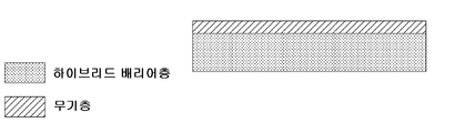
도 3a는 본 발명의 한 구체예에 따른 박막 투과 배리어 시스템의 단면을 도시한다.
도 3b는 본 발명의 한 구체예에 따른 박막 투과 배리어 시스템의 단면을 도시한다.
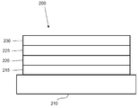
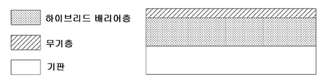
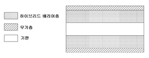
도 4는 본 발명의 한 구체예에 따른 배리어 시스템으로 코팅된 예시 기판의 단면을 도시하며; 도 4a는 배리어가 기판의 정상부에 코팅되어 있는 구성을 도시하고; 도 4b는 배리어가 기판의 저부에 코팅되어 있는 구성을 도시하며; 도 4c는 배리어가 기판의 정상부 및 저부에 코팅되어 잇는 구성을 도시한다.
도 5는 본 발명의 한 구체예에 따른 투과 배리어 시스템에서의 하향식 확산의 개략도를 도시한다.
도 6은 본 발명의 한 구체예에 따른 투과 배리어 시스템에서의 하향식 및 측방향 확산의 개략도를 도시한다.
도 7은 본 발명의 한 구체예에 따른 투과 배리어 시스템으로 캡슐화된 OLED에서의 하향식 확산 및 수평 방향 침입의 개략도를 도시한다.
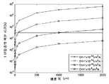
도 8은 본 발명의 한 구체예에 따른 시간의 함수로서의 투과된 물의 양의 플롯을 도시한다.
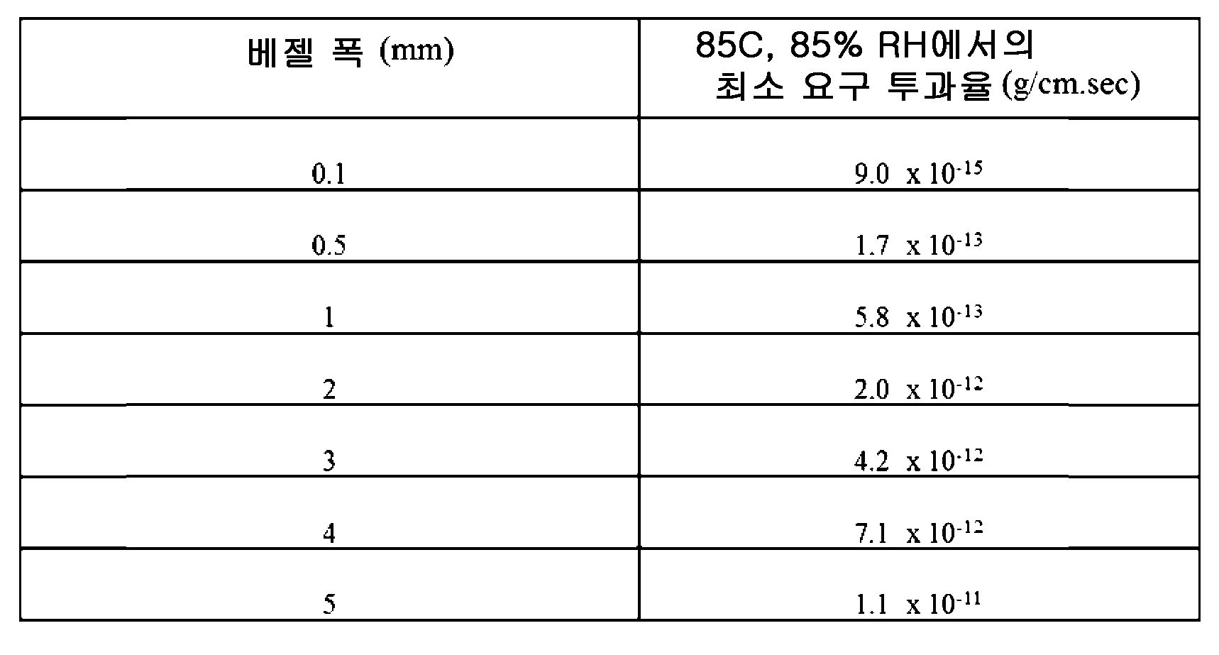
도 9는 본 발명의 한 구체예에 따른 베젤 폭의 함수로서의 물의 한 단일층의 확산 시간의 플롯을 도시한다.
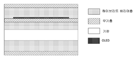
도 10은 본 발명의 한 구체예에 따른 투과 배리어 시스템으로 캡슐화된 기판 상의 OLED의 개략적 단면을 도시하며, 여기서 배리어 시스템은 OLED 성장 전에 기판 정상부에 증착되고, 또 다른 배리어 시스템이 OLED의 정상부에 증착된다.
도 11은 본 발명의 한 구체예에 따른 투과 배리어 시스템으로 캡슐화된 기판 상의 OLED의 개략적 단면을 도시하며, 여기서 배리어 시스템은 OLED 성장 전에 기판의 정상부 및 저부 모두에 증착되고, 또 다른 배리어 시스템이 OLED의 정상부에 증착된다.
도 12는 본 발명의 한 구체예에 따른 시간의 함수로서의 응력 변화의 플롯을 도시한다.
도 13은 시간들, T = 0(시간) 및 T = 24(시간)에서의 비교 OLED 디바이스의 사진을 도시한다.
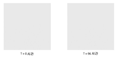
도 14는 시간들, T = 0(시간) 및 T = 96(시간)에서의 비교 OLED 디바이스 2의 사진을 도시한다.
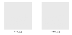
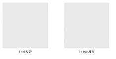
도 15는 T = 0(시간) 및 T = 500(시간)에서의, 본 발명의 한 구체예에 따른 OLED 디바이스의 사진을 도시한다.
도 16은 T = 0(시간) 및 T = 500(시간)에서의 본 발명에 한 구체예에 따른 OLED 디바이스의 사진을 도시한다.


Claims (20)
- 박막 배리어로서,
SiOxCyHz(여기서, 1 ≤ x < 2이고, 0.001 ≤ y ≤ 1이며, 0.001 ≤ z ≤ 1임)를 포함하는 제1 하이브리드 배리어층; 및
제1 하이브리드 배리어층에 바로 인접하게 배치되는 무기(inorganic) 제2 배리어층
을 포함하는 박막 배리어. - 제1항에 있어서, 박막 배리어는 제1 하이브리드 배리어층 및 무기 제2 배리어층으로 기본적으로 이루어지는 것인 박막 배리어.
- 제1항에 있어서, 제1 하이브리드 배리어의 두께가 0.05 ∼ 10 ㎛인 박막 배리어.
- 제1항에 있어서, 무기 제2 배리어층의 두께가 5 ∼ 1000 nm인 박막 배리어.
- 제1항에 있어서, 무기 제2 배리어층의 두께가 2 ∼ 20,000 nm인 박막 배리어.
- 제1항에 있어서, 무기층은 금속, 금속 산화물, 금속 질화물, 금속 옥시질화물(metal oxy-nitride), 금속 탄화물, 금속 붕화물 및 금속 옥시붕화물(metal oxy-boride)로 이루어진 군으로부터 선택되는 물질을 포함하는 것인 박막 배리어.
- 제1항에 있어서, 무기층은 산화규소, 산화알루미늄, 산화인듐, 산화주석, 산화아연, 인듐 주석 산화물, 인듐 아연 산화물, 알루미늄 아연 산화물, 산화탄탈, 산화지르코늄, 산화니오븀 및 산화몰리브덴으로 이루어진 군으로부터 선택되는 물질을 포함하는 것인 박막 배리어.
- 제1항에 있어서, 무기층은 질화규소, 질화알루미늄, 질화붕소, 탄화텅스텐, 탄화붕소, 탄화규소, 옥시붕화지르코늄, 옥시붕화티탄, 옥시질화알루미늄, 옥시질화규소, 및 옥시질화붕소로 이루어진 군으로부터 선택되는 물질을 포함하는 것인 박막 배리어.
- 제1항에 있어서, 하이브리드 배리어층은 38 C에서 10-9 cm2/sec 미만의 수증기 확산 계수를 갖는 것인 박막 배리어.
- 제1항에 있어서, 박막 배리어는 가요성인 박막 배리어.
- 제1항에 기재된 박막 배리어를 포함하는 유기 발광 소자(OLED).
- 제11항에 있어서, 박막 배리어는 OLED의 엣지를 너머 0.01 ∼ 10 mm 이하로 연장되는 것인 소자.
- 제11항에 있어서, OLED는 가요성 OLED이고, 박막 배리어는 가요성인 소자.
- 하나 이상의 전구물질을 얻는 단계로서, 하나 이상의 전구물질은 하나 이상의 유기규소 전구물질을 포함하는 것인 단계;
하나 이상의 전구물질 각각을 플라즈마 증착하여, 기판 위에 SiOxCyHz를 포함하는 배리어층을 형성시키는 단계; 및
배리어층에 바로 인접하게, 기판 위에 무기층을 증착하는 단계
를 포함하는 방법. - 제14항에 있어서, 배리어층은 기판과 무기층 사이에 배치되는 것인 방법.
- 제14항에 있어서, 배리어층 및 무기층 각각은 마스크의 사용 없이 증착하는 것인 방법.
- 제14항에 있어서, 배리어층 및 무기층 각각은 최소한으로서 하나의 마스크를 통해 증착하는 것인 방법.
- 제14항에 있어서, 배리어층 및 무기층은 단일의 공통 마스크를 통해 증착하는 것인 방법.
- 제14항에 있어서, 하나 이상의 전구물질은 Si, O, C 및 H를 포함하는 것인 방법.
- 제14항에 있어서, 하나 이상의 전구물질 각각은 단일 플라즈마 증착 공정으로 증착하는 것인 방법.
Applications Claiming Priority (2)
| Application Number | Priority Date | Filing Date | Title |
|---|---|---|---|
| US14/464,997 US20160056414A1 (en) | 2014-08-21 | 2014-08-21 | Thin film permeation barrier system for substrates and devices and method of making the same |
| US14/464,997 | 2014-08-21 |
Publications (2)
| Publication Number | Publication Date |
|---|---|
| KR20160028362A true KR20160028362A (ko) | 2016-03-11 |
| KR102321945B1 KR102321945B1 (ko) | 2021-11-04 |
Family
ID=55349036
Family Applications (1)
| Application Number | Title | Priority Date | Filing Date |
|---|---|---|---|
| KR1020150117982A Active KR102321945B1 (ko) | 2014-08-21 | 2015-08-21 | 기판 및 소자를 위한 박막 투과 배리어 시스템과 그의 제조 방법 |
Country Status (3)
| Country | Link |
|---|---|
| US (1) | US20160056414A1 (ko) |
| KR (1) | KR102321945B1 (ko) |
| CN (2) | CN105390621A (ko) |
Cited By (1)
| Publication number | Priority date | Publication date | Assignee | Title |
|---|---|---|---|---|
| KR20190117621A (ko) * | 2017-03-29 | 2019-10-16 | 데이진 가부시키가이샤 | 하드 코트층이 부착된 고분자 기판 |
Families Citing this family (12)
| Publication number | Priority date | Publication date | Assignee | Title |
|---|---|---|---|---|
| KR20150109984A (ko) * | 2014-03-21 | 2015-10-02 | 삼성전자주식회사 | 기체 차단 필름, 이를 포함하는 냉장고 및 기체 차단 필름의 제조방법 |
| WO2016190855A1 (en) * | 2015-05-27 | 2016-12-01 | Hewlett-Packard Development Company, L.P. | Articles having flexible substrates |
| KR102330331B1 (ko) * | 2015-07-17 | 2021-11-25 | 삼성디스플레이 주식회사 | 유기 발광 표시 장치 및 그 제조 방법 |
| KR102402606B1 (ko) * | 2015-10-19 | 2022-05-27 | 삼성디스플레이 주식회사 | 플렉서블 디스플레이 장치 및 그 제조방법 |
| CN105655494B (zh) * | 2016-03-18 | 2018-08-24 | 深圳市华星光电技术有限公司 | 有机发光二极管的基底及其制作方法、有机发光二极管 |
| US10483489B2 (en) * | 2016-08-12 | 2019-11-19 | Universal Display Corporation | Integrated circular polarizer and permeation barrier for flexible OLEDs |
| US11751426B2 (en) * | 2016-10-18 | 2023-09-05 | Universal Display Corporation | Hybrid thin film permeation barrier and method of making the same |
| WO2018130300A1 (en) * | 2017-01-13 | 2018-07-19 | Applied Materials, Inc. | Layer system adapted for use in an electro-optical device and method for manufacturing a layer system in a continuous roll-to-roll process |
| US11569447B2 (en) * | 2019-08-26 | 2023-01-31 | Wuhan China Star Optoelectronics Semiconductor Display Technology Co., Ltd. | Method for testing performance of thin-film encapsulation |
| US11362307B2 (en) | 2019-11-27 | 2022-06-14 | Applied Materials, Inc. | Encapsulation having polymer and dielectric layers for electronic displays |
| US11258045B2 (en) | 2019-11-27 | 2022-02-22 | Applied Materials, Inc. | Methods of forming stretchable encapsulation for electronic displays |
| US11211439B2 (en) | 2019-11-27 | 2021-12-28 | Applied Materials, Inc. | Stretchable polymer and dielectric layers for electronic displays |
Citations (5)
| Publication number | Priority date | Publication date | Assignee | Title |
|---|---|---|---|---|
| JP2003535939A (ja) * | 2000-06-06 | 2003-12-02 | ザ ダウ ケミカル カンパニー | ポリマー及び容器用の透過バリヤー層 |
| KR20050104401A (ko) * | 2003-02-26 | 2005-11-02 | 다우 코닝 코포레이션 | 수소화 규소 옥시카바이드 막의 제조방법 |
| US20070020451A1 (en) * | 2005-07-20 | 2007-01-25 | 3M Innovative Properties Company | Moisture barrier coatings |
| CN103258955A (zh) * | 2012-02-20 | 2013-08-21 | 中国科学院微电子研究所 | 有机电子器件的封装方法 |
| US20150159271A1 (en) * | 2013-12-09 | 2015-06-11 | Veeco Ald Inc. | Deposition of non-isostructural layers for flexible substrate |
Family Cites Families (11)
| Publication number | Priority date | Publication date | Assignee | Title |
|---|---|---|---|---|
| US6492026B1 (en) * | 2000-04-20 | 2002-12-10 | Battelle Memorial Institute | Smoothing and barrier layers on high Tg substrates |
| US20070054149A1 (en) * | 2005-08-23 | 2007-03-08 | Chi-Ming Cheng | Substrate assembly of a display device and method of manufacturing the same |
| US7767498B2 (en) * | 2005-08-25 | 2010-08-03 | Vitex Systems, Inc. | Encapsulated devices and method of making |
| US7621794B2 (en) * | 2005-11-09 | 2009-11-24 | International Display Systems, Inc. | Method of encapsulating an organic light-emitting device |
| US20080006819A1 (en) * | 2006-06-19 | 2008-01-10 | 3M Innovative Properties Company | Moisture barrier coatings for organic light emitting diode devices |
| CN101668879B (zh) * | 2007-03-28 | 2012-05-09 | 陶氏康宁公司 | 含硅和碳的阻挡层的卷到卷等离子体增强化学气相沉积方法 |
| JP5470969B2 (ja) * | 2009-03-30 | 2014-04-16 | 株式会社マテリアルデザインファクトリ− | ガスバリアフィルム、それを含む電子デバイス、ガスバリア袋、およびガスバリアフィルムの製造方法 |
| KR101718560B1 (ko) * | 2009-04-09 | 2017-03-21 | 스미또모 가가꾸 가부시키가이샤 | 가스 배리어성 적층 필름 |
| US8753711B2 (en) * | 2009-12-18 | 2014-06-17 | General Electric Company | Edge sealing method using barrier coatings |
| US20130236681A1 (en) * | 2012-03-06 | 2013-09-12 | Chang Min Lee | Photocurable composition, barrier layer including the same, and encapsulated apparatus including the same |
| CN103943789A (zh) * | 2014-04-18 | 2014-07-23 | 深圳市华星光电技术有限公司 | Oled器件及其制备方法 |
-
2014
- 2014-08-21 US US14/464,997 patent/US20160056414A1/en not_active Abandoned
-
2015
- 2015-08-19 CN CN201510511427.2A patent/CN105390621A/zh active Pending
- 2015-08-19 CN CN202010661902.5A patent/CN111769206A/zh active Pending
- 2015-08-21 KR KR1020150117982A patent/KR102321945B1/ko active Active
Patent Citations (5)
| Publication number | Priority date | Publication date | Assignee | Title |
|---|---|---|---|---|
| JP2003535939A (ja) * | 2000-06-06 | 2003-12-02 | ザ ダウ ケミカル カンパニー | ポリマー及び容器用の透過バリヤー層 |
| KR20050104401A (ko) * | 2003-02-26 | 2005-11-02 | 다우 코닝 코포레이션 | 수소화 규소 옥시카바이드 막의 제조방법 |
| US20070020451A1 (en) * | 2005-07-20 | 2007-01-25 | 3M Innovative Properties Company | Moisture barrier coatings |
| CN103258955A (zh) * | 2012-02-20 | 2013-08-21 | 中国科学院微电子研究所 | 有机电子器件的封装方法 |
| US20150159271A1 (en) * | 2013-12-09 | 2015-06-11 | Veeco Ald Inc. | Deposition of non-isostructural layers for flexible substrate |
Cited By (1)
| Publication number | Priority date | Publication date | Assignee | Title |
|---|---|---|---|---|
| KR20190117621A (ko) * | 2017-03-29 | 2019-10-16 | 데이진 가부시키가이샤 | 하드 코트층이 부착된 고분자 기판 |
Also Published As
| Publication number | Publication date |
|---|---|
| US20160056414A1 (en) | 2016-02-25 |
| KR102321945B1 (ko) | 2021-11-04 |
| CN105390621A (zh) | 2016-03-09 |
| CN111769206A (zh) | 2020-10-13 |
Similar Documents
| Publication | Publication Date | Title |
|---|---|---|
| KR102321945B1 (ko) | 기판 및 소자를 위한 박막 투과 배리어 시스템과 그의 제조 방법 | |
| US12446451B2 (en) | Electronic device with reduced non-device edge area | |
| KR102211205B1 (ko) | 전자 디바이스를 위한 엣지 장벽 필름 | |
| US20160254487A1 (en) | Permeation barrier system for substrates and devices and method of making the same | |
| US20190221771A1 (en) | Buffer layer for organic light emitting devices and method of making the same | |
| US20160118621A1 (en) | Hybrid barrier layer for substrates and electronic devices | |
| US11665951B2 (en) | Barrier film for electronic devices and substrates |
Legal Events
| Date | Code | Title | Description |
|---|---|---|---|
| PA0109 | Patent application |
St.27 status event code: A-0-1-A10-A12-nap-PA0109 |
|
| P22-X000 | Classification modified |
St.27 status event code: A-2-2-P10-P22-nap-X000 |
|
| PG1501 | Laying open of application |
St.27 status event code: A-1-1-Q10-Q12-nap-PG1501 |
|
| P22-X000 | Classification modified |
St.27 status event code: A-2-2-P10-P22-nap-X000 |
|
| A201 | Request for examination | ||
| PA0201 | Request for examination |
St.27 status event code: A-1-2-D10-D11-exm-PA0201 |
|
| E902 | Notification of reason for refusal | ||
| PE0902 | Notice of grounds for rejection |
St.27 status event code: A-1-2-D10-D21-exm-PE0902 |
|
| E13-X000 | Pre-grant limitation requested |
St.27 status event code: A-2-3-E10-E13-lim-X000 |
|
| P11-X000 | Amendment of application requested |
St.27 status event code: A-2-2-P10-P11-nap-X000 |
|
| P13-X000 | Application amended |
St.27 status event code: A-2-2-P10-P13-nap-X000 |
|
| E701 | Decision to grant or registration of patent right | ||
| PE0701 | Decision of registration |
St.27 status event code: A-1-2-D10-D22-exm-PE0701 |
|
| GRNT | Written decision to grant | ||
| PR0701 | Registration of establishment |
St.27 status event code: A-2-4-F10-F11-exm-PR0701 |
|
| PR1002 | Payment of registration fee |
St.27 status event code: A-2-2-U10-U11-oth-PR1002 Fee payment year number: 1 |
|
| PG1601 | Publication of registration |
St.27 status event code: A-4-4-Q10-Q13-nap-PG1601 |
|
| R18-X000 | Changes to party contact information recorded |
St.27 status event code: A-5-5-R10-R18-oth-X000 |
|
| P22-X000 | Classification modified |
St.27 status event code: A-4-4-P10-P22-nap-X000 |
|
| P22-X000 | Classification modified |
St.27 status event code: A-4-4-P10-P22-nap-X000 |
|
| P22-X000 | Classification modified |
St.27 status event code: A-4-4-P10-P22-nap-X000 |
|
| PR1001 | Payment of annual fee |
St.27 status event code: A-4-4-U10-U11-oth-PR1001 Fee payment year number: 4 |
|
| P22-X000 | Classification modified |
St.27 status event code: A-4-4-P10-P22-nap-X000 |
|
| P22-X000 | Classification modified |
St.27 status event code: A-4-4-P10-P22-nap-X000 |