KR20160028362A - Thin film permeation barrier system for substrates and devices and method of making the same - Google Patents
Thin film permeation barrier system for substrates and devices and method of making the same Download PDFInfo
- Publication number
- KR20160028362A KR20160028362A KR1020150117982A KR20150117982A KR20160028362A KR 20160028362 A KR20160028362 A KR 20160028362A KR 1020150117982 A KR1020150117982 A KR 1020150117982A KR 20150117982 A KR20150117982 A KR 20150117982A KR 20160028362 A KR20160028362 A KR 20160028362A
- Authority
- KR
- South Korea
- Prior art keywords
- barrier
- layer
- thin film
- inorganic
- barrier layer
- Prior art date
- Legal status (The legal status is an assumption and is not a legal conclusion. Google has not performed a legal analysis and makes no representation as to the accuracy of the status listed.)
- Granted
Links
Images


Classifications
-
- C—CHEMISTRY; METALLURGY
- C23—COATING METALLIC MATERIAL; COATING MATERIAL WITH METALLIC MATERIAL; CHEMICAL SURFACE TREATMENT; DIFFUSION TREATMENT OF METALLIC MATERIAL; COATING BY VACUUM EVAPORATION, BY SPUTTERING, BY ION IMPLANTATION OR BY CHEMICAL VAPOUR DEPOSITION, IN GENERAL; INHIBITING CORROSION OF METALLIC MATERIAL OR INCRUSTATION IN GENERAL
- C23C—COATING METALLIC MATERIAL; COATING MATERIAL WITH METALLIC MATERIAL; SURFACE TREATMENT OF METALLIC MATERIAL BY DIFFUSION INTO THE SURFACE, BY CHEMICAL CONVERSION OR SUBSTITUTION; COATING BY VACUUM EVAPORATION, BY SPUTTERING, BY ION IMPLANTATION OR BY CHEMICAL VAPOUR DEPOSITION, IN GENERAL
- C23C16/00—Chemical coating by decomposition of gaseous compounds, without leaving reaction products of surface material in the coating, i.e. chemical vapour deposition [CVD] processes
- C23C16/22—Chemical coating by decomposition of gaseous compounds, without leaving reaction products of surface material in the coating, i.e. chemical vapour deposition [CVD] processes characterised by the deposition of inorganic material, other than metallic material
- C23C16/30—Deposition of compounds, mixtures or solid solutions, e.g. borides, carbides, nitrides
-
- H—ELECTRICITY
- H10—SEMICONDUCTOR DEVICES; ELECTRIC SOLID-STATE DEVICES NOT OTHERWISE PROVIDED FOR
- H10K—ORGANIC ELECTRIC SOLID-STATE DEVICES
- H10K77/00—Constructional details of devices covered by this subclass and not covered by groups H10K10/80, H10K30/80, H10K50/80 or H10K59/80
- H10K77/10—Substrates, e.g. flexible substrates
- H10K77/111—Flexible substrates
-
- H01L51/5096—
-
- H01L21/02109—
-
- H01L21/02118—
-
- H01L21/02205—
-
- H01L51/0011—
-
- H01L51/56—
-
- H—ELECTRICITY
- H10—SEMICONDUCTOR DEVICES; ELECTRIC SOLID-STATE DEVICES NOT OTHERWISE PROVIDED FOR
- H10K—ORGANIC ELECTRIC SOLID-STATE DEVICES
- H10K50/00—Organic light-emitting devices
- H10K50/80—Constructional details
- H10K50/84—Passivation; Containers; Encapsulations
- H10K50/844—Encapsulations
-
- H—ELECTRICITY
- H10—SEMICONDUCTOR DEVICES; ELECTRIC SOLID-STATE DEVICES NOT OTHERWISE PROVIDED FOR
- H10K—ORGANIC ELECTRIC SOLID-STATE DEVICES
- H10K2102/00—Constructional details relating to the organic devices covered by this subclass
- H10K2102/301—Details of OLEDs
- H10K2102/311—Flexible OLED
-
- H—ELECTRICITY
- H10—SEMICONDUCTOR DEVICES; ELECTRIC SOLID-STATE DEVICES NOT OTHERWISE PROVIDED FOR
- H10K—ORGANIC ELECTRIC SOLID-STATE DEVICES
- H10K59/00—Integrated devices, or assemblies of multiple devices, comprising at least one organic light-emitting element covered by group H10K50/00
- H10K59/80—Constructional details
- H10K59/87—Passivation; Containers; Encapsulations
- H10K59/873—Encapsulations
-
- Y—GENERAL TAGGING OF NEW TECHNOLOGICAL DEVELOPMENTS; GENERAL TAGGING OF CROSS-SECTIONAL TECHNOLOGIES SPANNING OVER SEVERAL SECTIONS OF THE IPC; TECHNICAL SUBJECTS COVERED BY FORMER USPC CROSS-REFERENCE ART COLLECTIONS [XRACs] AND DIGESTS
- Y02—TECHNOLOGIES OR APPLICATIONS FOR MITIGATION OR ADAPTATION AGAINST CLIMATE CHANGE
- Y02E—REDUCTION OF GREENHOUSE GAS [GHG] EMISSIONS, RELATED TO ENERGY GENERATION, TRANSMISSION OR DISTRIBUTION
- Y02E10/00—Energy generation through renewable energy sources
- Y02E10/50—Photovoltaic [PV] energy
- Y02E10/549—Organic PV cells
Landscapes
- Chemical & Material Sciences (AREA)
- Physics & Mathematics (AREA)
- Optics & Photonics (AREA)
- Inorganic Chemistry (AREA)
- General Chemical & Material Sciences (AREA)
- Chemical Kinetics & Catalysis (AREA)
- Engineering & Computer Science (AREA)
- Materials Engineering (AREA)
- Mechanical Engineering (AREA)
- Metallurgy (AREA)
- Organic Chemistry (AREA)
- Electroluminescent Light Sources (AREA)
Abstract
본 발명은 박막 투과 배리어 시스템 및 그를 제조하는 기술을 제공한다. 배리어 시스템은 하이브리드층, 예컨대 SiOxCyHz를 함유하는 층, 및 무기층을 포함한다.The present invention provides a thin film transmission barrier system and a technique for manufacturing the same. The barrier system comprises a hybrid layer, for example a layer containing SiO x C y H z , and an inorganic layer.
Description
당해 발명은 합동 산학 연구 협약에 따라 리전츠 오브 더 유니버시티 오브 미시간, 프린스턴 유니버시티, 더 유니버시티 오브 서던 캘리포니아 및 더 유니버셜 디스플레이 코포레이션 당사자 중 하나 이상에 의하여, 이를 대신하여 및/또는 이와 관련하여 완성되었다. 협약은 당해 발명이 완성된 일자에 그리고 일자 이전에 발효되었으며, 당해 발명은 협약서의 범주내에서 수행된 활동의 결과로서 완성되었다.The present invention was completed and / or in place of and / or in accordance with the Joint Industry-Academic Research Agreement by one or more of the Regents of the University of Michigan, Princeton University, the University of Southern California, and the Universal Display Corporation. The Convention entered into force on the date of completion of the invention and prior to its date, and the invention was completed as a result of the activities carried out within the scope of the agreement.
발명의 분야Field of invention
본 발명은 유기 발광 소자(OLED) 및 유사 소자, 그리고 그에 포함된 여러 가지 층들에 관한 것이다. 보다 구체적으로는, 본 발명은 OLED 또는 기타 유사 소자 또는 기판과 함께 사용하기에 적합한 투과 배리어에 관한 것이다.The present invention relates to organic light emitting devices (OLEDs) and similar devices, and the various layers contained therein. More particularly, the present invention relates to a transmission barrier suitable for use with an OLED or other similar device or substrate.
유기 물질을 사용하는 광전자 디바이스는 여러 이유로 인하여 점차로 중요해지고 있다. 이와 같은 디바이스를 제조하는데 사용되는 다수의 물질은 비교적 저렴하여 유기 광전자 디바이스는 무기 디바이스에 비하여 경제적 잇점면에서 잠재성을 갖는다. 또한, 유기 물질의 고유한 성질, 예컨대 이의 가요성은 가요성 기판상에서의 제조와 같은 특정 적용예에 매우 적합하게 될 수 있다. 유기 광전자 디바이스의 예로는 유기 발광 디바이스(OLED), 유기 광트랜지스터, 유기 광전지 및 유기 광검출기를 들 수 있다. OLED의 경우, 유기 물질은 통상의 물질에 비하여 성능면에서의 잇점을 가질 수 있다. 예를 들면, 유기 발광층이 광을 방출하는 파장은 일반적으로 적절한 도펀트로 용이하게 조절될 수 있다.BACKGROUND OF THE INVENTION Optoelectronic devices using organic materials are becoming increasingly important for a variety of reasons. Many of the materials used to fabricate such devices are relatively inexpensive, and organic optoelectronic devices have the potential to be economically advantageous over inorganic devices. In addition, the inherent properties of organic materials, such as their flexibility, can be very well suited for certain applications, such as on flexible substrates. Examples of organic optoelectronic devices include organic light emitting devices (OLEDs), organic phototransistors, organic photovoltaic cells, and organic photodetectors. In the case of OLEDs, organic materials may have performance advantages over conventional materials. For example, the wavelength at which the organic light emitting layer emits light can generally be readily controlled with suitable dopants.
OLED는 디바이스를 가로질러 전압을 인가시 광을 방출하는 유기 박막을 사용하게 한다. OLED는 평판 패널 디스플레이, 조명 및 역광과 같은 적용예에 사용하기 위한 점차로 중요해지는 기술이다. 여러가지의 OLED 물질 및 형상은 미국 특허 제5,844,363호, 제6,303,238호 및 제5,707,745호에 기재되어 있으며, 이들 특허 문헌은 그 전문이 본원에 참고로 포함된다.OLEDs use organic thin films that emit light when a voltage is applied across the device. OLEDs are an increasingly important technology for use in applications such as flat panel displays, lighting and backlighting. Various OLED materials and shapes are described in U.S. Patent Nos. 5,844,363, 6,303,238, and 5,707,745, the disclosures of which are incorporated herein by reference in their entirety.
인광 발광 분자에 대한 하나의 적용예는 총 천연색 디스플레이이다. 이러한 디스플레이에 대한 산업적 기준은 "포화" 색상으로서 지칭하는 특정 색상을 방출하도록 조정된 픽셀을 필요로 한다. 특히, 이러한 기준은 포화 적색, 녹색 및 청색 픽셀을 필요로 한다. 색상은 당업계에 공지된 CIE 좌표를 사용하여 측정될 수 있다.One application for phosphorescent molecules is the total color display. The industry standard for such displays requires pixels that are adjusted to emit a particular color referred to as a "saturation" color. In particular, these criteria require saturated red, green and blue pixels. The color may be measured using CIE coordinates known in the art.
녹색 발광 분자의 일례로는 하기 화학식을 갖는 Ir(ppy)3으로 나타낸 트리스(2-페닐피리딘) 이리듐이다:An example of a green light emitting molecule is tris (2-phenylpyridine) iridium represented by Ir (ppy) 3 having the following formula:

본원에서의 이와 같은 화학식 및 하기의 화학식에서, 본 출원인은 질소로부터 금속(여기에서는 Ir)으로의 배위결합을 직선으로 도시한다.In such formulas and the following formulas in the present application, Applicants show a coordinate bond from nitrogen to metal (here Ir) in a straight line.
본원에서, 용어 "유기"라는 것은 유기 광전자 디바이스를 제조하는데 사용될 수 있는 중합체 물질뿐 아니라, 소분자 유기 물질을 포함한다. "소분자"는 중합체가 아닌 임의의 유기 물질을 지칭하며, "소분자"는 실제로 꽤 클 수도 있다. 소분자는 일부의 상황에서는 반복 단위를 포함할 수 있다. 예를 들면, 치환기로서 장쇄 알킬 기를 사용하는 것은 "소분자" 유형으로부터 분자를 제거하지 않는다. 소분자는 또한 예를 들면 중합체 주쇄상에서의 측쇄기로서 또는 주쇄의 일부로서 중합체에 투입될 수 있다. 소분자는 또한 코어 부분상에 생성된 일련의 화학적 셸로 이루어진 덴드리머의 코어 부분으로서 작용할 수 있다. 덴드리머의 코어 부분은 형광 또는 인광 소분자 이미터일 수 있다. 덴드리머는 "소분자"일 수 있으며, OLED 분야에서 통상적으로 사용되는 모든 덴드리머는 소분자인 것으로 밝혀졌다.As used herein, the term "organic" includes not only polymeric materials that can be used to make organic optoelectronic devices, but also small molecule organic materials. "Small molecule" refers to any organic material that is not a polymer, and "small molecule" may actually be quite large. Small molecules may contain repeat units in some situations. For example, using a long chain alkyl group as a substituent does not remove the molecule from the "small molecule" type. The small molecule may also be introduced into the polymer, for example as a side chain group on the polymer backbone or as part of the backbone. The small molecule can also act as a core part of the dendrimer consisting of a series of chemical shells formed on the core part. The core portion of the dendrimer may be a fluorescent or phosphorescent small molecule emitter. The dendrimer may be a "small molecule ", and all the dendrimers conventionally used in the field of OLEDs have been found to be small molecules.
본원에서 사용한 바와 같이, "정상부"는 기판으로부터 가장 멀리 떨어졌다는 것을 의미하며, "저부"는 기판에 가장 근접하다는 것을 의미한다. 제1층이 제2층"의 정상부에 위치하는" 것으로 기재될 경우, 제1층은 기판으로부터 멀리 떨어져 배치된다. 제1층이 제2층과 "접촉되어 있는" 것으로 명시되지 않는다면 제1층과 제2층 사이에는 다른 층이 존재할 수 있다. 예를 들면, 캐소드와 애노드의 사이에 다양한 유기층이 존재할 수 있을지라도, 캐소드는 애노드"의 상부에 위치하는" 것으로 기재될 수 있다.As used herein, "top" means farthest from the substrate, and "bottom" means closest to the substrate. When the first layer is described as " located at the top of the second layer ", the first layer is disposed away from the substrate. Other layers may be present between the first and second layers, unless the first layer is specified as "in contact" with the second layer. For example, although various organic layers may be present between the cathode and the anode, the cathode may be described as being " located at the top of the anode ".
본원에서 사용한 바와 같이, "용액 가공성"은 용액 또는 현탁액 형태로 액체 매체에 용해, 분산 또는 수송될 수 있거나 및/또는 액체 매체로부터 증착될 수 있다는 것을 의미한다.As used herein, "solution processibility" means that it can be dissolved, dispersed or transported in liquid medium in the form of a solution or suspension, and / or deposited from a liquid medium.
리간드가 발광 물질의 광활성 성질에 직접적으로 기여하는 것으로 밝혀질 경우, 리간드는 "광활성"으로서 지칭될 수 있다. 보조적 리간드가 광활성 리간드의 성질을 변경시킬 수 있을지라도, 리간드가 발광 물질의 광활성 성질에 기여하지 않는 것으로 밝혀질 경우, 리간드는 "보조적"인 것으로 지칭될 수 있다. When the ligand is found to contribute directly to the photoactive properties of the luminescent material, the ligand can be referred to as "photoactive ". Although the auxiliary ligand may alter the nature of the photoactive ligand, the ligand may be referred to as "auxiliary" if it is found that the ligand does not contribute to the photoactive properties of the luminescent material.
본원에서 사용한 바와 같이 그리고 일반적으로 당업자가 이해하고 있는 바와 같이, 제1의 "최고 점유 분자 오르비탈"(HOMO) 또는 "최저 비점유 분자 오르비탈"(LUMO) 에너지 준위가 진공 에너지 준위에 근접할 경우, 제1의 에너지 준위는 제2의 HOMO 또는 LUMO보다 "더 크거나" 또는 "더 높다". 이온화 전위(IP)가 진공 레벨에 대하여 음의 에너지로서 측정되므로, 더 높은 HOMO 에너지 준위는 더 작은 절대값을 갖는 IP에 해당한다(IP는 음의 값이 더 작다). 유사하게, 더 높은 LUMO 에너지 준위는 절대값이 더 작은 전자 친화도(EA)에 해당한다(EA의 음의 값이 더 작다). 상부에서의 진공 레벨을 갖는 통상의 에너지 준위 다이어그램에서, 물질의 LUMO 에너지 준위는 동일한 물질의 HOMO 에너지 준위보다 더 높다. "더 높은" HOMO 또는 LUMO 에너지 준위는 "더 낮은" HOMO 또는 LUMO 에너지 준위보다 상기 다이어그램의 상부에 더 근접한다는 것을 나타낸다.As used herein, and as generally understood by those skilled in the art, the first "highest occupied molecular orbital" (HOMO) or "lowest unoccupied molecular orbital" (LUMO) energy level is close to the vacuum energy level , The first energy level is "greater" or "higher" than the second HOMO or LUMO. Since the ionization potential (IP) is measured as negative energy with respect to the vacuum level, the higher HOMO energy level corresponds to an IP with a smaller absolute value (IP has a smaller negative value). Similarly, a higher LUMO energy level corresponds to an electron affinity (EA) with an absolute value smaller (the negative value of EA is smaller). In a typical energy level diagram with a vacuum level at the top, the LUMO energy level of the material is higher than the HOMO energy level of the same material. The "higher" HOMO or LUMO energy level is closer to the top of the diagram than the "lower" HOMO or LUMO energy level.
본원에서 사용한 바와 같이 그리고 일반적으로 당업자가 이해하는 바와 같이, 제1의 일 함수의 절대값이 더 클 경우, 제1의 일 함수는 제2의 일 함수보다 "더 크거나" 또는 "더 높다". 일 함수는 일반적으로 진공 레벨에 대하여 음의 수로서 측정되므로, 이는 "더 높은" 일 함수의 음의 값이 더 크다는 것을 의미한다. 상부에서 진공 레벨을 갖는 통상의 에너지 준위 다이어그램에서, "더 높은" 일 함수는 진공 레벨로부터 아래 방향으로 더 먼 것으로서 도시된다. 그래서, HOMO 및 LUMO 에너지 준위의 정의는 일 함수와는 상이한 조약을 따른다.As used herein, and as generally understood by those skilled in the art, if the absolute value of the first work function is greater, then the first work function is "greater" or " . Since the work function is generally measured as a negative number with respect to the vacuum level, this means that the negative value of the "higher" work function is greater. In a typical energy level diagram with a vacuum level at the top, the "higher" work function is shown as being farther down from the vacuum level. Thus, the definition of the HOMO and LUMO energy levels follows a treaty different from the work function.
OLED에 대한 세부사항 및 전술한 정의는 미국 특허 제7,279,704호에서 찾아볼 수 있으며, 이 특허 문헌의 개시내용은 그 전문이 본원에 참고로 포함된다.The details of the OLED and the above definition can be found in U.S. Patent No. 7,279,704, the disclosure of which is incorporated herein by reference in its entirety.
한 구체예에서, SiOxCyHz를 포함하는 제1 하이브리드 배리어층 및 제1 하이브리드 배리어층에 바로 인접하게 배치되는 무기(inorganic) 제2 배리어층을 포함하는 박막 배리어가 제공된다. 박막 배리어는 오직 제1 하이브리드 배리어층 및 무기 제2 배리어층을 포함하거나, 또는 기본적으로 이들로 이루어질 수 있다. 박막 배리어는 가요성일 수 있고, 민감한 디바이스, 예컨대 OLED를 캡슐화하거나, 아니면 보호하기 위해 사용될 수 있다.In one embodiment, a thin film barrier is provided that includes a first hybrid barrier layer comprising SiO x C y H z and an inorganic second barrier layer disposed immediately adjacent to the first hybrid barrier layer. The thin film barrier may comprise, or consist essentially of, a first hybrid barrier layer and an inorganic second barrier layer. The thin film barrier can be flexible and can be used to encapsulate or otherwise protect sensitive devices, such as OLEDs.
한 구체예에서, 박막 배리어는 하나 이상의 유기규소 함유 전구물질를 얻는 단계, 전구물질 각각을 플라즈마 증착하여 기판 위에 SiOxCyHz를 포함하는 배리어층을 형성하는 단계, 기판 위에, 그리고 배리어층에 바로 인접하게 무기층을 증착하는 단계에 의해 제조될 수 있다. 배리어층은 무기층의 위 또는 아래에 증착될 수 있으며, 층들의 조합이 기판의 한쪽 면 또는 양면에 증착될 수 있다. 층들을 증착하는 데에는 하나 이상의 마스크가 사용될 수 있고, 두 층들을 증착하는 데에는 단일 마스크가 사용될 수 있다. 층 들은 어떠한 마스크의 사용 없이 증착될 수도 있다.In one embodiment, the thin film barrier comprises the steps of obtaining one or more organosilicon containing precursors, plasma depositing each of the precursors to form a barrier layer comprising SiO x C y H z on the substrate, By depositing an inorganic layer immediately adjacent to it. The barrier layer may be deposited above or below the inorganic layer, and combinations of layers may be deposited on one or both sides of the substrate. One or more masks may be used to deposit the layers, and a single mask may be used to deposit the two layers. The layers may be deposited without the use of any mask.
도 1은 유기 발광 소자를 도시한다.
도 2는 별도의 전자 수송층을 갖지 않는 인버트형 유기 발광 소자를 도시한다.
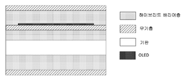
도 3a는 본 발명의 한 구체예에 따른 박막 투과 배리어 시스템의 단면을 도시한다.
도 3b는 본 발명의 한 구체예에 따른 박막 투과 배리어 시스템의 단면을 도시한다.
도 4는 본 발명의 한 구체예에 따른 배리어 시스템으로 코팅된 예시 기판의 단면을 도시하며; 도 4a는 배리어가 기판의 정상부에 코팅되어 있는 구성을 도시하고; 도 4b는 배리어가 기판의 저부에 코팅되어 있는 구성을 도시하며; 도 4c는 배리어가 기판의 정상부 및 저부에 코팅되어 잇는 구성을 도시한다.
도 5는 본 발명의 한 구체예에 따른 투과 배리어 시스템에서의 하향식 확산의 개략도를 도시한다.
도 6은 본 발명의 한 구체예에 따른 투과 배리어 시스템에서의 하향식 및 측방향 확산의 개략도를 도시한다.
도 7은 본 발명의 한 구체예에 따른 투과 배리어 시스템으로 캡슐화된 OLED에서의 하향식 확산 및 수평 방향 침입의 개략도를 도시한다.
도 8은 본 발명의 한 구체예에 따른 시간의 함수로서의 투과된 물의 양의 플롯을 도시한다.
도 9는 본 발명의 한 구체예에 따른 베젤 폭의 함수로서의 물의 한 단일층의 확산 시간의 플롯을 도시한다.
도 10은 본 발명의 한 구체예에 따른 투과 배리어 시스템으로 캡슐화된 기판 상의 OLED의 개략적 단면을 도시하며, 여기서 배리어 시스템은 OLED 성장 전에 기판 정상부에 증착되고, 또 다른 배리어 시스템이 OLED의 정상부에 증착된다.
도 11은 본 발명의 한 구체예에 따른 투과 배리어 시스템으로 캡슐화된 기판 상의 OLED의 개략적 단면을 도시하며, 여기서 배리어 시스템은 OLED 성장 전에 기판의 정상부 및 저부 모두에 증착되고, 또 다른 배리어 시스템이 OLED의 정상부에 증착된다.
도 12는 본 발명의 한 구체예에 따른 시간의 함수로서의 응력 변화의 플롯을 도시한다.
도 13은 시간들, T = 0(시간) 및 T = 24(시간)에서의 비교 OLED 디바이스의 사진을 도시한다.
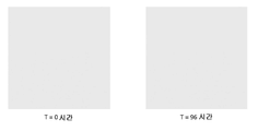
도 14는 시간들, T = 0(시간) 및 T = 96(시간)에서의 비교 OLED 디바이스 2의 사진을 도시한다.
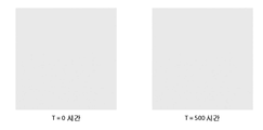
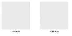
도 15는 T = 0(시간) 및 T = 500(시간)에서의, 본 발명의 한 구체예에 따른 OLED 디바이스의 사진을 도시한다.
도 16은 T = 0(시간) 및 T = 500(시간)에서의 본 발명에 한 구체예에 따른 OLED 디바이스의 사진을 도시한다.1 shows an organic light emitting device.
Fig. 2 shows an invert-type organic light emitting device having no separate electron transport layer.
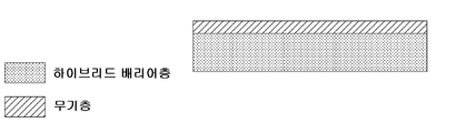
3A shows a cross section of a thin film transmission barrier system in accordance with one embodiment of the present invention.
Figure 3B illustrates a cross section of a thin film transmission barrier system in accordance with one embodiment of the present invention.
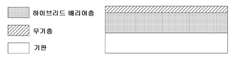
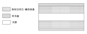
Figure 4 illustrates a cross-section of an exemplary substrate coated with a barrier system in accordance with one embodiment of the present invention; 4A shows a configuration in which a barrier is coated on a top portion of a substrate; 4B shows a configuration in which the barrier is coated on the bottom of the substrate; 4C shows a configuration in which the barrier is coated on the top and bottom of the substrate.
Figure 5 shows a schematic of top down diffusion in a transmission barrier system in accordance with one embodiment of the present invention.
Figure 6 shows a schematic of top-down and lateral diffusion in a transmission barrier system in accordance with one embodiment of the present invention.
Figure 7 shows a schematic diagram of a top-down diffusion and a horizontal orientation in an OLED encapsulated with a transmission barrier system according to one embodiment of the present invention.
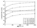
Figure 8 shows a plot of the amount of water permeated as a function of time in accordance with one embodiment of the present invention.
Figure 9 shows a plot of diffusion time of a single layer of water as a function of bezel width in accordance with one embodiment of the present invention.
Figure 10 shows a schematic cross-section of an OLED on a substrate encapsulated with a transmissive barrier system according to one embodiment of the present invention wherein the barrier system is deposited atop the substrate before OLED growth and another barrier system is deposited at the top of the OLED do.
Figure 11 shows a schematic cross-section of an OLED on a substrate encapsulated with a transmissive barrier system according to one embodiment of the present invention wherein the barrier system is deposited at both the top and bottom of the substrate prior to OLED growth, As shown in FIG.
Figure 12 shows a plot of stress variation as a function of time in accordance with one embodiment of the present invention.
Figure 13 shows a photograph of a comparative OLED device at times T = 0 (time) and T = 24 (time).
14 shows a photograph of a
Figure 15 shows a photograph of an OLED device according to one embodiment of the present invention at T = 0 (time) and T = 500 (time).
Figure 16 shows a photograph of an OLED device according to one embodiment of the present invention at T = 0 (time) and T = 500 (time).
일반적으로, OLED는 애노드 및 캐소드 사이에 배치되어 이에 전기 접속되는 1종 이상의 유기층을 포함한다. 전류가 인가되면, 애노드는 정공을 유기층(들)에 주입하고, 캐소드는 전자를 주입한다. 주입된 정공 및 전자는 각각 반대로 하전된 전극을 향하여 이동한다. 전자 및 정공이 동일한 분자상에 편재화될 경우, 여기된 에너지 상태를 갖는 편재화된 전자-정공쌍인 "엑시톤"이 형성된다. 엑시톤이 광발광 메카니즘에 의하여 이완될 경우 광이 방출된다. 일부의 경우에서, 엑시톤은 엑시머 또는 엑시플렉스상에 편재화될 수 있다. 비-방사 메카니즘, 예컨대 열 이완도 또한 발생할 수 있으나, 일반적으로 바람직하지 않은 것으로 간주된다.Generally, an OLED comprises at least one organic layer disposed between and electrically connected to the anode and the cathode. When an electric current is applied, the anode injects holes into the organic layer (s), and the cathode injects electrons. The injected holes and electrons move inversely toward the charged electrodes, respectively. When electrons and holes are localized on the same molecule, an "exciton" is formed, which is a unionized electron-hole pair having an excited energy state. Light is emitted when the excitons are relaxed by the light emitting mechanism. In some cases, the excitons can be localized on the excimer or exciplex. Non-radiating mechanisms such as thermal relaxation may also occur, but are generally considered undesirable.
초기 OLED는 예를 들면 미국 특허 제 4,769,292호에 개시된 바와 같은 일중항 상태로부터 광("형광")을 방출하는 발광 분자를 사용하였으며, 상기 특허 문헌은 그 전문이 본원에 참고로 포함된다. 형광 방출은 일반적으로 10 나노초 미만의 시간 기간으로 발생한다.Early OLEDs use luminescent molecules that emit light ("fluorescence") from a singlet state as disclosed, for example, in U.S. Patent No. 4,769,292, the disclosure of which is incorporated herein by reference in its entirety. Fluorescent emission generally occurs in a time period of less than 10 nanoseconds.
보다 최근에는, 삼중항 상태로부터의 광("인광")을 방출하는 발광 물질을 갖는 OLED가 예시되어 있다. 문헌[Baldo et al., "Highly Efficient Phosphorescent Emission from Organic Electroluminescent Devices," Nature, vol. 395, 151-154, 1998 ("Baldo-I")] 및 [Baldo et al., "Very high-efficiency green organic light-emitting devices based on electrophosphorescence," Appl. Phys. Lett., vol. 75, No. 3, 4-6 (1999) ("Baldo-II")]을 참조하며, 이들 문헌은 그 전문이 본원에 참고로 포함된다. 인광은 참고로 포함되는 미국 특허 제7,279,704호의 컬럼 5-6에 보다 구체적으로 기재되어 있다.More recently, an OLED having a luminescent material that emits light from a triplet state ("phosphorescence") is illustrated. Baldo et al., "Highly Efficient Phosphorescent Emission from Organic Electroluminescent Devices," Nature , vol. 395, 151-154, 1998 ("Baldo-I") and Baldo et al., "Very high-efficiency green organic light-emitting devices based on electrophosphorescence," Appl. Phys. Lett. , vol. 75, No. 3, 4-6 (1999) ("Baldo-II"), the disclosures of which are incorporated herein by reference in their entirety. Phosphorescence is more specifically described in column 5-6 of U.S. Patent No. 7,279,704, which is incorporated by reference.
도 1은 유기 발광 디바이스(100)를 도시한다. 도면은 반드시 축척에 의하여 도시하지는 않았다. 디바이스(100)는 기판(110), 애노드(115), 정공 주입층(120), 정공 수송층(125), 전자 차단층(130), 발광층(135), 정공 차단층(140), 전자 수송층(145), 전자 주입층(150), 보호층(155), 캐소드(160) 및 차단층(170)을 포함할 수 있다. 캐소드(160)는 제1의 전도층(162) 및 제2의 전도층(164)을 갖는 화합물 캐소드이다. 디바이스(100)는 기재된 순서로 층을 증착시켜 제조될 수 있다. 이들 다양한 층뿐 아니라, 예시의 물질의 성질 및 기능은 참고로 포함되는 미국 특허 제7,279,704호의 컬럼 6-10에 보다 구체적으로 기재되어 있다.Figure 1 illustrates an organic
이들 각각의 층에 대한 더 많은 예도 이용 가능하다. 예를 들면 가요성 및 투명한 기판-애노드 조합은 미국 특허 제 5,844,363호에 개시되어 있으며, 이 특허 문헌은 그 전문이 본원에 참고로 포함된다. p-도핑된 정공 수송층의 예는 미국 특허 출원 공개 공보 제2003/0230980호에 개시된 바와 같이, 50:1의 몰비로 F4-TCNQ로 도핑된 m-MTDATA이며, 이 특허 문헌은 그 전문이 본원에 참고로 포함된다. 발광 및 호스트 물질의 예는 미국 특허 제6,303,238호(Thompson et al.)에 개시되어 있으며, 이 특허 문헌은 그 전문이 본원에 참고로 포함된다. n-도핑된 전자 수송층의 예는 미국 특허 출원 공개 공보 제2003/0230980호에 개시된 바와 같이, 1:1의 몰비로 Li로 도핑된 BPhen이고, 이 특허 문헌은 그 전문이 본원에 참고로 포함된다. 그 전문이 본원에 참고로 포함되는 미국 특허 제5,703,436호 및 제5,707,745호에는 적층된 투명, 전기전도성 스퍼터-증착된 ITO 층을 갖는 Mg:Ag와 같은 금속의 박층을 갖는 화합물 캐소드를 비롯한 캐소드의 예가 개시되어 있다. 차단층의 이론 및 용도는 미국 특허 제 6,097,147호 및 미국 특허 출원 공개 공보 제2003/0230980호에 보다 구체적으로 기재되어 있으며, 이들 특허 문헌은 그 전문이 본원에 참고로 포함된다. 주입층의 예는 미국 특허 출원 공개 공보 제2004/0174116호에 제공되어 있으며, 이 특허 문헌은 그 전문이 본원에 참고로 포함된다. 보호층의 설명은 미국 특허 출원 공개 공보 제2004/0174116호에서 찾아볼 수 있으며, 이들 특허 문헌은 그 전문이 본원에 참고로 포함된다.More examples for each of these layers are available. For example, a flexible and transparent substrate-anode combination is disclosed in U.S. Patent No. 5,844,363, which is incorporated herein by reference in its entirety. An example of a p-doped hole transport layer is m-MTDATA doped with F 4 -TCNQ at a molar ratio of 50: 1, as disclosed in U.S. Patent Application Publication 2003/0230980, ≪ / RTI > Examples of luminescent and host materials are disclosed in U.S. Patent No. 6,303,238 (Thompson et al.), Which is incorporated herein by reference in its entirety. An example of an n-doped electron transporting layer is BPhen doped with Li at a molar ratio of 1: 1 as disclosed in U.S. Patent Application Publication 2003/0230980, which patent application is incorporated herein by reference in its entirety . U.S. Patents 5,703,436 and 5,707,745, which are hereby incorporated by reference in their entirety, disclose a cathode including a compound cathode having a thin layer of metal such as Mg: Ag with a transparent, electrically conductive sputter-deposited ITO layer deposited thereon Lt; / RTI > The theory and use of barrier layers are more specifically described in U.S. Patent No. 6,097,147 and U.S. Patent Application Publication No. 2003/0230980, which are incorporated herein by reference in their entirety. An example of an injection layer is provided in U.S. Patent Application Publication No. 2004/0174116, which is incorporated herein by reference in its entirety. A description of the protective layer can be found in U.S. Patent Application Publication No. 2004/0174116, which is incorporated herein by reference in its entirety.
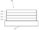
도 2는 인버트형 OLED(200)를 도시한다. 디바이스는 기판(210), 캐소드(215), 발광층(220), 정공 수송층(225) 및 애노드(230)를 포함한다. 디바이스(200)는 기재된 순서로 층을 적층시켜 제조될 수 있다. 가장 흔한 OLED 구조는 애노드의 위에 캐소드가 배치되어 있고 디바이스(200)가 애노드(230)의 아래에 캐소드(215)가 배치되어 있으므로, 디바이스(200)는 "인버트형" OLED로 지칭될 수 있다. 디바이스(100)에 관하여 기재된 것과 유사한 물질이 디바이스(200)의 해당 층에 사용될 수 있다. 도 2는 디바이스(100)의 구조로부터 일부 층이 얼마나 생략될 수 있는지의 일례를 제공한다.FIG. 2 shows an
도 1 및 도 2에 도시된 단순 적층된 구조는 비제한적인 예로서 제공하며, 본 발명의 실시양태는 다양한 기타의 구조와 관련하여 사용될 수 있는 것으로 이해하여야 한다. 기재된 특정한 물질 및 구조는 사실상 예시를 위한 것이며, 기타의 물질 및 구조도 사용될 수 있다. 작용성 OLED는 기재된 다양한 층을 상이한 방식으로 조합하여 달성될 수 있거나 또는 층은 디자인, 성능 및 비용 요인에 기초하여 전적으로 생략할 수 있다. 구체적으로 기재되지 않은 기타의 층도 또한 포함될 수 있다. 이들 구체적으로 기재된 층을 제외한 물질을 사용할 수 있다. 본원에 제공된 다수의 예가 단일 물질을 포함하는 것으로서 다양한 층을 기재하기는 하나, 물질, 예컨대 호스트 및 도펀트의 혼합물 또는 보다 일반적으로 혼합물을 사용할 수 있다. 또한, 층은 다수의 하부층을 가질 수 있다. 본원에서 다양한 층에 제시된 명칭은 엄격하게 제한하고자 하는 것은 아니다. 예를 들면, 디바이스(200)에서 정공 수송층(225)은 정공을 수송하며, 정공을 발광층(220)에 주입하며, 정공 수송층 또는 정공 주입층으로서 기재될 수 있다. 하나의 실시양태에서, OLED는 캐소드와 애노드 사이에 배치된 "유기층"을 갖는 것으로 기재될 수 있다. 이러한 유기층은 단일층을 포함할 수 있거나 또는 예를 들면 도 1 및 도 2와 관련하여 기재된 바와 같은 상이한 유기 물질의 복수의 층을 더 포함할 수 있다.It should be understood that the simple laminated structure shown in Figures 1 and 2 is provided by way of non-limiting example, and that embodiments of the present invention may be used in conjunction with various other structures. The particular materials and structures described are for illustration purposes only and other materials and structures may be used. Functional OLEDs may be achieved by combining the various layers described in different ways, or the layers may be entirely omitted based on design, performance and cost factors. Other layers not specifically described may also be included. Materials other than those specifically described can be used. While many of the examples provided herein describe various layers as including a single material, a mixture of materials, such as a host and a dopant, or more generally a mixture, may be used. In addition, the layer may have a plurality of underlying layers. The nomenclature presented in the various layers herein is not intended to be strictly limiting. For example, in the
구체적으로 기재하지 않은 구조 및 물질, 예컨대 미국 특허 제 5,247,190호(Friend et al.)에 기재된 바와 같은 중합체 물질(PLED)을 포함하는 OLED를 사용할 수 있으며, 이 특허 문헌은 그 전문이 본원에 참고로 포함된다. 추가의 예로서, 단일 유기층을 갖는 OLED를 사용할 수 있다. OLED는 예를 들면 미국 특허 제 5,707,745호(Forrest et al.)에 기재된 바와 같이 적층될 수 있으며, 이 특허 문헌은 그 전문이 본원에 참고로 포함된다. OLED 구조는 도 1 및 도 2에 도시된 단순 적층된 구조로부터 벗어날 수 있다. 예를 들면, 기판은 미국 특허 제 6,091,195호(Forrest et al.)에 기재된 바와 같은 메사형(mesa) 구조 및/또는 미국 특허 제 5,834,893호(Bulovic et al.)에 기재된 피트형(pit) 구조와 같은 아웃-커플링(out-coupling)을 개선시키기 위한 각진 반사면을 포함할 수 있으며, 이들 특허 문헌은 그 전문이 본원에 참고로 포함된다.An OLED including a polymer material (PLED) as described in U.S. Patent No. 5,247,190 (Friend et al.), Which is not specifically described, may be used, . As a further example, an OLED having a single organic layer can be used. OLEDs may be deposited, for example, as described in U.S. Patent No. 5,707,745 (Forrest et al.), Which is incorporated herein by reference in its entirety. The OLED structure may deviate from the simple laminated structure shown in Figs. 1 and 2. For example, the substrate may have a mesa structure as described in U.S. Patent No. 6,091,195 (Forrest et al.) And / or a pit structure as described in U.S. Patent No. 5,834,893 (Bulovic et al. And may include angled reflective surfaces to improve the same out-coupling, the disclosures of which are incorporated herein by reference in their entirety.
반대의 의미로 명시하지 않는 한, 다양한 실시양태의 임의의 층은 임의의 적절한 방법에 의하여 적층될 수 있다. 유기층의 경우, 바람직한 방법으로는 미국 특허 제6,013,982호 및 제6,087,196호(이 특허 문헌은 그 전문이 본원에 참고로 포함됨)에 기재된 바와 같은 열 증발, 잉크-제트, 미국 특허 제 6,337,102호(Forrest et al.)(이 특허 문헌은 그 전문이 본원에 참고로 포함됨)에 기재된 바와 같은 유기 증기상 증착(OVPD), 미국 특허 출원 제10/233,470호(이 특허 문헌은 그 전문이 본원에 참고로 포함됨)에 기재된 바와 같은 유기 증기 제트 프린팅(OVJP)에 의한 증착을 들 수 있다. 기타의 적절한 증착 방법은 스핀 코팅 및 기타의 용액계 공정을 포함한다. 용액계 공정은 질소 또는 불활성 분위기 중에서 실시되는 것이 바람직하다. 기타의 층의 경우, 바람직한 방법은 열 증발을 포함한다. 바람직한 패턴 형성 방법은 마스크를 통한 증착, 미국 특허 제6,294,398호 및 제6,468,819호(이 특허 문헌은 그 전문이 본원에 참고로 포함됨)에 기재된 바와 같은 냉간 용접 및, 잉크-제트 및 OVJD와 같은 일부 증착 방법과 관련된 패턴 형성을 포함한다. 증착시키고자 하는 물질은 특정한 증착 방법과 상용성을 갖도록 변형될 수 있다. 예를 들면, 분지형 또는 비분지형, 바람직하게는 3개 이상의 탄소를 포함하는 알킬 및 아릴 기와 같은 치환기는 이의 용액 가공의 처리 능력을 향상시키기 위하여 소분자에 사용될 수 있다. 20개 이상의 탄소를 갖는 치환기를 사용할 수 있으며, 3 내지 20개의 탄소가 바람직한 범위이다. 비대칭 구조를 갖는 물질은 대칭 구조를 갖는 것보다 더 우수한 용액 가공성을 가질 수 있는데, 비대칭 물질은 재결정화되는 경향이 낮을 수 있기 때문이다. 덴드리머 치환기는 용액 가공을 처리하는 소분자의 능력을 향상시키기 위하여 사용될 수 있다.Unless otherwise stated, any layer of the various embodiments may be deposited by any suitable method. In the case of the organic layer, preferred methods include thermal evaporation, ink-jet, as described in U.S. Patent Nos. 6,013,982 and 6,087,196 (the patent application is incorporated herein by reference), U.S. Patent No. 6,337,102 Organic Vapor Deposition (OVPD), as described in U.S. Patent Application Serial No. 10 / 233,470, which is incorporated herein by reference in its entirety, (OVJP) as described in < RTI ID = 0.0 > J. < / RTI > Other suitable deposition methods include spin coating and other solution-based processes. The solution-type process is preferably carried out in nitrogen or an inert atmosphere. For other layers, the preferred method involves thermal evaporation. Preferred patterning methods include deposition via a mask, cold welding as described in U.S. Patent Nos. 6,294,398 and 6,468,819, which are incorporated herein by reference, and some deposition such as ink-jet and OVJD And pattern formation associated with the method. The material to be deposited may be modified to have compatibility with a particular deposition method. Substituents such as, for example, alkyl and aryl groups, whether branched or unbranched, preferably containing at least 3 carbons, can be used in small molecules to improve their processing capabilities in solution processing. Substituents having 20 or more carbons can be used, with 3 to 20 carbons being preferred. Materials with an asymmetric structure may have better solution processability than those with a symmetric structure, since asymmetric materials may be less prone to recrystallization. Dendrimer substituents can be used to enhance the ability of small molecules to process solution processing.
본 발명의 실시양태에 의하여 제조된 디바이스는 차단층을 추가로 임의로 포함할 수 있다. 차단층의 하나의 목적은 전극 및 유기층이 수분, 증기 및/또는 기체 등을 포함하는 환경에서 유해한 종에 대한 노출로 인하여 손상되지 않도록 한다. 차단층은 기판의 위에서, 기판의 아래에서 또는 기판의 옆에서, 전극 또는, 엣지를 포함하는 디바이스의 임의의 기타 부분의 위에서 증착될 수 있다. 차단층은 단일층 또는 다중층을 포함할 수 있다. 차단층은 각종 공지의 화학적 증착 기법에 의하여 형성될 수 있으며 복수의 상을 갖는 조성물뿐 아니라 단일 상을 갖는 조성물을 포함할 수 있다. 임의의 적절한 물질 또는 물질의 조합을 차단층에 사용할 수 있다. 차단층은 무기 또는 유기 화합물 또는 둘다를 혼입할 수 있다. 바람직한 차단층은 미국 특허 제7,968,146호, PCT 특허 출원 번호 PCT/US2007/023098 및 PCT/US2009/042829에 기재된 바와 같은 중합체 물질 및 비-중합체 물질의 혼합물을 포함하며, 이들 문헌의 개시내용은 본원에 그 전문이 참고로 포함된다. "혼합물"을 고려하면, 차단층을 포함하는 전술한 중합체 및 비-중합체 물질은 동일한 반응 조건하에서 및/또는 동일한 시간에서 증착되어야만 한다. 중합체 대 비-중합체 물질의 중량비는 95:5 내지 5:95 범위내일 수 있다. 중합체 및 비-중합체 물질은 동일한 전구체 물질로부터 생성될 수 있다. 한 예에서, 중합체 및 비-중합체 물질의 혼합물은 본질적으로 중합체 규소 및 무기 규소로 이루어진다.Devices fabricated according to embodiments of the present invention may further optionally include a barrier layer. One purpose of the barrier layer is to prevent damage to the electrode and the organic layer due to exposure to the harmful species in an environment that includes moisture, vapors and / or gases, and the like. The barrier layer may be deposited on top of the substrate, below the substrate, or on the side of the substrate, above the electrode or any other part of the device comprising the edge. The barrier layer may comprise a single layer or multiple layers. The barrier layer may be formed by various known chemical vapor deposition techniques and may include a composition having a plurality of phases as well as a composition having a single phase. Any suitable material or combination of materials may be used for the barrier layer. The barrier layer may incorporate inorganic or organic compounds or both. Preferred barrier layers include polymeric materials and mixtures of non-polymeric materials as described in U.S. Patent No. 7,968,146, PCT Patent Application Nos. PCT / US2007 / 023098 and PCT / US2009 / 042829, the disclosures of which are incorporated herein by reference That specialization is included as a reference. With the consideration of "mixture ", the aforementioned polymeric and non-polymeric materials comprising the barrier layer must be deposited under the same reaction conditions and / or at the same time. The weight ratio of polymer to non-polymeric material may be in the range of 95: 5 to 5:95. Polymer and non-polymeric materials may be produced from the same precursor material. In one example, the mixture of polymeric and non-polymeric materials consists essentially of polymeric silicon and inorganic silicon.
본 발명의 실시양태에 의하여 제조되는 디바이스는 평판 패널 디스플레이, 컴퓨터 모니터, 의료용 모니터, 텔레비젼, 광고판, 실내 또는 옥외 조명 및/또는 시그날링을 위한 라이트, 헤드업 디스플레이, 완전 투명 디스플레이, 플렉시블 디스플레이, 레이저 프린터, 전화기, 휴대폰, 개인용 정보 단말기(PDA), 랩탑 컴퓨터, 디지탈 카메라, 캠코더, 뷰파인더, 마이크로디스플레이, 3D 디스플레이, 자동차, 거대 월, 극장 또는 스타디움 스크린 또는 간판을 비롯한 다양한 소비재에 투입될 수 있다. 패시브 매트릭스 및 액티브 매트릭스를 비롯한 다양한 조절 메카니즘을 사용하여 본 발명에 의한 디바이스를 조절할 수 있다. 디바이스의 대다수는 사람에게 안락감을 주는 온도 범위, 예컨대 18℃ 내지 30℃, 더욱 바람직하게는 실온(20℃ 내지 25℃)에서 사용되도록 한 것이나, 이 온도 범위를 벗어나, 예를 들어 -40℃ 내지 +80℃에서 사용될 수도 있다.Devices manufactured according to embodiments of the present invention may be used in various applications such as flat panel displays, computer monitors, medical monitors, televisions, billboards, lights for indoor or outdoor lighting and / or signaling, heads up displays, Can be put into a variety of consumer goods including printers, telephones, mobile phones, personal digital assistants (PDAs), laptop computers, digital cameras, camcorders, viewfinders, microdisplays, 3D displays, automobiles, gigantic walls, theaters or stadium screens or signs . Various adjustment mechanisms, including passive matrix and active matrix, may be used to adjust the device according to the present invention. The majority of the devices are intended to be used in a temperature range that gives comfort to human beings, such as 18 to 30 DEG C, more preferably room temperature (20 to 25 DEG C), but outside this temperature range, + 80 < 0 > C.
본원에 기재된 물질 및 구조는 OLED를 제외한 디바이스에서의 적용예를 가질 수 있다. 예를 들면, 기타의 광전자 디바이스, 예컨대 유기 태양 전지 및 유기 광검출기는 물질 및 구조를 사용할 수 있다. 보다 일반적으로, 유기 디바이스, 예컨대 유기 트랜지스터는 물질 및 구조를 사용할 수 있다.The materials and structures described herein may have applications in devices other than OLEDs. For example, other optoelectronic devices such as organic solar cells and organic photodetectors can use materials and structures. More generally, organic devices, such as organic transistors, can use materials and structures.
OLED 디스플레이 및 조명 패널은 대개, 대기 기체, 특히 수분 및 산소로부터 확실한 보호를 받는 것이 이롭다. 전극으로서 사용되는 화학 반응성의 낮은 일함수 금속은 대개, 이들 종의 존재 하에서 불안정하며, 기저의 유기층으로부터 층 박리될 수 있다. 흔히 사용되는 유기 발광 물질은 또한, 물에 노출시 비발광성 켄칭 종(quenching species)을 형성할 수 있다. 통상, 보호는 대개 OLED를 캡슐화하는 것 및 두 유리판 사이의 건조제에 의해 제공되며, 이들은 엣지 부근이 접착제로 밀봉된다. 이 종래의 캡슐화 방법은 디바이스를 강고하게 하므로, 가요성 OLED의 캡슐화에는 사용할 수 없다. OLED 디스플레이를 가요성이고 경량으로 만들기 위해서, 경질 유리판 대신에 얇은 가요성 배리어 막이 사용될 수 있다.OLED displays and lighting panels are generally beneficial to be reliably protected from atmospheric gases, especially moisture and oxygen. The chemically reactive low work function metals used as electrodes are generally unstable in the presence of these species and can be delaminated from the underlying organic layer. Commonly used organic luminescent materials can also form non-luminescent quenching species upon exposure to water. Typically, protection is usually provided by encapsulating the OLED and a desiccant between the two glass plates, which are sealed with an adhesive near the edge. This conventional encapsulation method makes the device strong, so it can not be used for encapsulation of flexible OLEDs. In order to make the OLED display flexible and lightweight, a thin flexible barrier film may be used instead of a hard glass plate.
가요성 OLED의 제조에 사용되는 폴리머 기판, 예컨대 폴리 에틸렌 테레프탈레이트(PET), 폴리 에틸렌 나프탈레이트(PEN) 등은 본질적으로 수분 배리어 특성이 부족할 수 있다. 예를 들어, 100 ㎛ 두께의 PET의 수증기 투과 속도(WVTR)는 37.8C 및 40C에서 각각, 대략 3.9 및 17 g/m2/day이다. 10,000 시간의 OLED 수명에 요구되는 수증기 투과 속도(WVTR)에 대해 가장 널리 언급되는 값은 10-6 g/m2/day이다. 마찬가지로, 비슷한 수명에 있어서 산소 투과 속도(OTR)는 10-5 cm3/m2/day ∼ 10-3 cm3/m2/day의 어딘가인 것으로 보고되어 있다[예컨대, 문헌(Lewis and Weaver, "Thin Film Permeation_Barrier Technology for Flexible Organic Light Emtting Devices", IEEE Journal of Selected Topics in Quantum Electronics, Vol. 10, No. 1, p.45, Jan/Feb 2004)]. 또한, 디스플레이의 하나 이상의 표면은, OLED에 의해 발생되는 광을 투과시키기 위해서, 투명한 배리어 막으로 보호되어야 한다. OLED 위에 코팅될 경우, 대개는 실온에서 또는 그 부근의 온도에서 배리어 막을 증착하는 것이 바람직한데, 높은 온도가 기저의 OLED를 손상시킬 것이기 때문이다. 다수의 무기 물질, 예컨대 Si3N4, SiO2 및 Al2O3가 대기 기체에 대해 낮은 투과율을 갖긴 하나, 무기 산화물 및 질화물로부터 투명한 캡슐화 배리어 막을 제조하는 것은 어렵운 것으로 업계에 입증되어 있는데, 이들이 실온 또는 실온 부근에서 박막으로서 증착될 경우 투과성이 되기 때문이다. 첫째로, 단일의 무기 배리어층은 실온에서 증착시에 미세한 결함을 갖는다. 이들 결함은, 문헌[Erlat, "SiOx Gas Barrier Coatings on Polymer Substrates: 형상 and Gas Transport Considerations", J. Phys. Chem. B, 1999, 103, 6047-55)]에 보고된 바로는, 수증기를 포함하는 대기 기체가 투과하는 경로를 형성할 수 있다. 둘째로, 무기 박막(배리어층), 예컨대 SiOx, SiNx 또는 SiOxNy는 임계 두께에 도달하면 자기 경감형(self-relief) 미세 균열이 발생할 수 있는데, 이는 궁극적으로 투과 배리어 특성을 제한할 수 있다. 마지막으로, 임계의 균열 변형 값은 OLED 디바이스의 전반적인 가요성을 제한할 수 있다. 이들 단일 무기층의 균열 변형은 두께의 함수이다. 예를 들어, 100 nm ITO 층의 균열 변형은 약 1%이다.Polymer substrates such as polyethylene terephthalate (PET), polyethylenenaphthalate (PEN), etc., which are used in the manufacture of flexible OLEDs, may inherently lack moisture barrier properties. For example, the water vapor transmission rate (WVTR) of 100 탆 thick PET is approximately 3.9 and 17 g / m 2 / day at 37.8C and 40C, respectively. The most widely mentioned value for water vapor transmission rate (WVTR) required for an OLED lifetime of 10,000 hours is 10 -6 g / m 2 / day. Similarly, the oxygen permeation rate (OTR) is reported to be somewhere around 10 -5 cm 3 / m 2 / day to 10 -3 cm 3 / m 2 / day for similar lifetimes (see, eg, Lewis and Weaver, "Thin Film Permeation_Barrier Technology for Flexible Organic Light Emitting Devices", IEEE Journal of Selected Topics in Quantum Electronics, Vol.10, No.1, p.45, Jan / Feb 2004). In addition, one or more surfaces of the display must be protected with a transparent barrier film to transmit light generated by the OLED. When coated over an OLED, it is generally desirable to deposit a barrier film at or near room temperature, because a high temperature will damage the underlying OLED. Although many inorganic materials such as Si 3 N 4 , SiO 2 and Al 2 O 3 have low transmittance to atmospheric gases, it has proven difficult to manufacture transparent encapsulating barrier films from inorganic oxides and nitrides, And they become transparent when they are deposited as a thin film at room temperature or near room temperature. First, a single inorganic barrier layer has a minute defect at the time of deposition at room temperature. These defects, literature [Erlat, "SiO x Gas Barrier Coatings on Polymer Substrates: shape and Gas Transport Considerations", J. Phys . Chem. B, 1999, 103, 6047-55), it is possible to form a path through which atmospheric gas containing water vapor passes. Second, self-relief microcracks can occur when the inorganic thin film (barrier layer), such as SiO x , SiN x, or SiO x N y , reaches a critical thickness, which ultimately limits the barrier properties can do. Finally, the critical crack deformation value may limit the overall flexibility of the OLED device. The crack deformation of these single inorganic layers is a function of thickness. For example, the crack deformation of a 100 nm ITO layer is about 1%.
가요성 박막 배리어는 기판 및 전자 기기용 캡슐화제로서 이전에 입증되었다. 미국 특허 제6,548,912호, 제6,268,695호, 제6,413,645호 및 제6,522,067호에는 감습 장치 및 기판을 캡슐화하기 위해서 "다중" 배리어 스택 및/또는 다이애드(dyad)의 다양한 배열이 기술되어 있다. 각각의 배리어 스택 쌍 또는 다이애드는 무기 물질 및 고분자층 쌍을 포함한다. 대기 기체에 대해 낮은 투과율을 갖는 무기층, 일반적으로 금속 산화물, 예컨대 Al2O3가 배리어층의 역할을 한다. 다결정질 Al2O3는 통상적으로 실온에서 반응 스퍼터링에 의해 증착된다. 이들 막은 흔히 미세한 결함, 예컨대 핀홀, 크랙 및 결정립계를 함유하며, 그것들은 결국 수증기를 포함하는 대기 기체의 투과 경로를 형성한다. 고분자층은 통상적으로 폴리아크릴레이트 물질이고, 이것은 액체 아크릴레이트 모노머의 순간 증발에 의해 증착되며, 이후 상기 모노머는 UV 방사선 또는 전자 빔에 의해 경화된다. 이 고분자층은, 미국 특허 제6,570,325호에 개시된 바와 같이, 무기층 내의 결함들을 기계적으로 탈결합시킬 수 있다. 다중 다이애드(흔히 약 3 ∼ 5 개의 다이애드, 즉 6 ∼ 10 개의 층)를 사용함으로써, 이들 배리어 막이 경질의 무기층들을 서로 기계적으로 탈결합시키고 물 및 산소에게 긴 투과 경로를 강요하여 이들 분자가 OLED에 도달는 데에 긴 시간이 걸리게 하는 것에 의해 기저 디바이스를 보호할 수 있다. 이 방법은 다이애드를 통한 수증기의 하향식 확산에 긴 지연 시간을 제공할 수 있긴 하나, OLED를 직접 캡슐화하는 데에 사용될 경우에 수증기의 측방향/엣지 확산을 조절하기 어렵다. 고분자층/탈결합층은 수증기에 대해 높은 확산 계수를 갖기 때문에, 보호에는 매우 넓은 엣지 시일(edge seal)이 필요하다. 엣지 시일 폭을 줄이는 한 가지 방법이 미국 특허 제7,198,832호에 개시되어 있으며, 그 개시내용은 전부 참고로 인용되어 있다. 이 방법에서는, 주어진 배리어 스택 중, 무기 배리어층의 면적이 탈결합층, 즉, 고분자층의 면적보다 크게 제조된다. 이후, 제2 배리어 스택의 면적은 제1 배리어 스택 등등의 면적보다 커야한다. 이 구조를 취함으로써, 배리어층은 수증기 및 산소의 측방향/엣지 확산에 대한 보호를 제공할 수 있다.Flexible thin film barriers have been previously demonstrated as encapsulating agents for substrates and electronics. U.S. Patent Nos. 6,548,912, 6,268,695, 6,413,645, and 6,522,067 describe various arrangements of "multi" barrier stacks and / or dyads to encapsulate a humidifier and a substrate. Each barrier stack pair or die add comprises an inorganic material and a polymer layer pair. An inorganic layer, typically a metal oxide, such as Al 2 O 3 , having a low transmittance to atmospheric gas acts as a barrier layer. Polycrystalline Al 2 O 3 is typically deposited by reactive sputtering at room temperature. These membranes often contain microscopic defects such as pinholes, cracks and grain boundaries, which eventually form the permeate path of the atmospheric gas containing water vapor. The polymer layer is typically a polyacrylate material, which is deposited by instantaneous evaporation of liquid acrylate monomers, which are then cured by UV radiation or electron beams. This polymer layer can mechanically debond bonds in the inorganic layer, as disclosed in U.S. Patent No. 6,570,325. By using multiple die attaches (often about 3 to 5 diesads, or 6 to 10 layers), these barrier membranes mechanically debond the rigid inorganic layers together and force a long transmission path to water and oxygen, Lt; RTI ID = 0.0 > OLED. ≪ / RTI > While this method can provide a long delay time for the top-down diffusion of water vapor through the die add, it is difficult to control the lateral / edge diffusion of water vapor when used to encapsulate the OLED directly. Since the polymer layer / debonding layer has a high diffusion coefficient for water vapor, a very wide edge seal is required for protection. One method of reducing the edge seal width is disclosed in U.S. Patent No. 7,198,832, the disclosure of which is incorporated herein by reference in its entirety. In this method, of the given barrier stack, the area of the inorganic barrier layer is made larger than the area of the debonding layer, that is, the polymer layer. Then, the area of the second barrier stack must be larger than the area of the first barrier stack and the like. By taking this structure, the barrier layer can provide protection against lateral / edge diffusion of water vapor and oxygen.
종래의 다층 배리어 시스템은 단점이 있을 수 있다. 고분자층/탈결합층, 일반적으로 아크릴레이트는, 수증기에 대해 높은 확산 계수를 가질 수 있다. OLED의 직접 캡슐화에 종래의 다층 배리어가 사용될 경우, 이 높은 확산 계수는 얻을 수 있는 최소 엣지 폭에 근본적인 제한을 줄 수 있는데, 무기 배리어층의 풋프린트(footprint)가 탈결합층, 즉, 고분자층의 면적보다 크게 제조되어야 하기 때문이다. 이후, 제2 배리어 스택의 풋프린트는, 양호한 엣지 시일을 얻기 위해 제1 배리어 스택 등등의 면적보다 커야 한다. 이는 다중 마스크의 사용을 필요로 할 수 있으며, 이는 결국 빈번한 마스크 세정을 필요로 하면서 전체 공정을 번잡하게 만들고 TAKT 시간을 현저히 증가시킨다. 예를 들어 미국 특허 공보 제2014/170785호에는, 다중 마스크의 사용을 필요로 하는 결과, 제조 동안에 마스크의 처리 및 이송에 많은 수고를 쏟아야 하는 다양한 시스템 및 기술이 기재되어 있다. 그에 반해, 본원에 보다 상세히 기술된 바와 같이, 본 발명의 구체예는 보다 적은 마스크를 사용함으로써 이러한 문제를 피할 수 있다.Conventional multilayer barrier systems can have drawbacks. The polymer layer / decoupling layer, generally acrylate, may have a high diffusion coefficient for water vapor. When a conventional multilayer barrier is used for direct encapsulation of an OLED, this high diffusion coefficient can give a fundamental limitation to the minimum edge width achievable, since the footprint of the inorganic barrier layer is the de- As compared with the case of the first embodiment. The footprint of the second barrier stack should then be larger than the area of the first barrier stack, etc., to obtain a good edge seal. This may necessitate the use of multiple masks, which ultimately necessitates frequent mask cleaning and makes the whole process complicated and significantly increases the TAKT time. For example, U.S. Patent Publication No. 2014/170785 discloses various systems and techniques that require the use of multiple masks, and that require a great deal of effort in processing and transporting the masks during fabrication. In contrast, embodiments of the present invention, as described in more detail herein, avoid this problem by using fewer masks.
또한, 엣지 폭 또는 베젤 폭은 디스플레이의 사용 불가 부분이다. 이들 기술을 이용하여 거의 제로의 엣지 또는 엣지가 없는 디스플레이를 얻는 것은 어렵거나 불가능 할 수 있다.Also, the edge width or bezel width is an unusable part of the display. Using these techniques, it can be difficult or impossible to obtain a display with almost zero edges or no edges.
다른 단점은, 고품질 무기 배리어층을 얻기 위해서 무기 배리어층, 예컨대 스퍼팅된 금속 산화물층의 증착 속도가, 고분자층에 비해 낮게 유지될 수 있다는 점일 수 있다. 이는 TAKT 시간을 증가시킨다.Another disadvantage can be that the deposition rate of the inorganic barrier layer, for example the sputtered metal oxide layer, can be kept lower than that of the polymer layer in order to obtain a high quality inorganic barrier layer. This increases the TAKT time.
다른 단점은 뱃치 공정 동안에 발생할 수 있는데, 이 공정에서는 기판이 스퍼터 챔버(진공) 사이에서 불활성 분위기 챔버(비진공)로 다수회(예컨대, 6 ∼ 8 회) 이동되어서 모노머층을 순간 증발시켜야 할 수 있다. 웹 공정(web processing)에서는, 다층을 증착하기 위해서 복수의 스퍼터 타겟 및 모노머 공급원이 필요할 수 있다. 이들 각각은 또한 비용 및 TAKT 시간을 증가시킨다.Another disadvantage may arise during the batch process in which the substrate is moved between the sputter chambers (vacuum) in an inert atmosphere chamber (non-vacuum) a number of times (e.g., 6-8 times) to evaporate the monomer layer instantaneously have. In web processing, a plurality of sputter targets and monomer sources may be required to deposit multiple layers. Each of these also increases cost and TAKT time.
일반적으로, 배리어 시스템은 몇몇 주요한 요건, 즉, 수분에 대한 비교적 낮은 투과율(바람직하게는 최소 개수의 층과 더불은 것); 엣지에서의 충분한 시일(바람직하게는 비교적 작은 엣지 폭과 더불은 것); 및 비교적 높은 가요성을 충족시키는 것이 바람직할 수 있다.In general, the barrier system has several key requirements: a relatively low transmittance for moisture (preferably with a minimum number of layers); Sufficient seal at the edge (preferably with a relatively small edge width); And it may be desirable to satisfy relatively high flexibility.
비교적 낮은 투과율에 대한 필요성에 관하여, 전술한 바와 같이, 수분 및 산소에 기인하는 OLED 디바이스의 분해를 방지하기 위해서는 효과적인 캡슐화가 요구된다. 캡슐화 배리어의 배리어 특성은 두 가지 확산 파라미터, 즉, 투과율 P = g/(cm sec atm) 및 증기 투과 속도 VTR = g/(m2 day)에 있어서 측정될 수 있다. 단일 배리어를 통한 기체(OLED의 경우에는, 일반적으로 수증기 또는 산소)의 투과율 P는, P = DS로 정의되며, 여기서 S(g/(cm3 atm))은 배리어 물질 중 기체의 용해도이고, D는 배리어 물질 중 기체의 확산 계수이다. 용해도는 투과 물질이 막에 얼마나 용해될 수 있는가를 판정하는 것인 반면, 확산 계수는 투과 물질이 막 물질 내에서 얼마나 빠르게 이동할 수 있는가를 판정하는 것이다. 수증기의 투과 속도(WVTR) 및 산소의 투과 속도(OTR)는 캡슐화의 배리어 특성의 척도이다. 이들은, 주어진 배리어 두께에 대해 주어진 온도 및 상대 습도에 있어서 명시된다. 앞서 개시한 바와 같이, 10000 시간의 OLED 저장 수명(50% 유효 면적 수축)에 있어서 수증기 투과 속도에 대해 통상 언급되는 요건은 10-6 g/m2/day이다. 마찬가지로, 유사한 수명에 있어서 요구되는 산소 투과 속도(OTR)는 10-5 cm3/m2/day ∼ 10-3 cm3/m2/day 범위이다. OLED 디바이스의 수명을 명시하기 위한 더 직접적인 방식은, 가속된 환경 시험 조건(높은 온도, 높은 상대 습도)에서 수명을 이용하는 것이다. 널리 이용되는 공업적 OLED 저장 수명 요건은 특정 용도(디스플레이 또는 조명)에 좌우되고, a) 85C, 85% 상대 습도에서 240 시간(10일), 또는 b) 85C, 85% 상대 습도에서 500 시간(∼3주) 후, 5% 미만의 유효 면적 수축으로서 명시된다.As regards the need for a relatively low transmittance, effective encapsulation is required to prevent degradation of OLED devices due to moisture and oxygen, as described above. The barrier properties of the encapsulation barrier can be measured at two diffusion parameters, i.e., transmittance P = g / (cm sec atm) and vapor permeation rate VTR = g / (m 2 day). Gas through a single barrier and permeability P is defined as P = DS (in the case of the OLED is, in general, the water vapor or oxygen), in which a solubility of the barrier material S (g / (cm 3 atm)) gas, D Is the diffusion coefficient of the gas in the barrier material. The solubility is to determine how far the permeable material can be dissolved in the membrane, while the diffusion coefficient is to determine how fast the permeable material can move within the membrane material. The permeation rate of water vapor (WVTR) and the permeation rate of oxygen (OTR) are measures of the barrier properties of encapsulation. These are specified for a given temperature and relative humidity for a given barrier thickness. As previously described, the requirement typically referred to for water vapor transmission rate for an OLED storage lifetime of 10000 hours (50% effective area shrinkage) is 10 -6 g / m 2 / day. Similarly, the oxygen permeation rate (OTR) required for a similar lifetime is in the range of 10 -5 cm 3 / m 2 / day to 10 -3 cm 3 / m 2 / day. A more direct way to specify the lifetime of an OLED device is to use the lifetime in accelerated environmental test conditions (high temperature, high relative humidity). The widely used industrial OLED shelf life requirements depend on the particular application (display or illumination) and include: a) 85 hours at 85 C, 85% relative humidity for 240 hours (10 days), or b) 85 hours at 85% To 3 weeks), it is specified as an effective area contraction of less than 5%.
바람직한 엣지 특성에 관해서는, 일반적으로 배리어 시스템이, OLED를 수분 및 산소의 측방향 확산으로부터 보호하는 것이 바람직하다. 바람직하게는, 배리어 막은 최소 엣지 폭/베젤 요건과 더불어 우수한 엣지 시일을 제공해야 한다. 최소 베젤 폭은 특정 용도 및/또는 제작 공차에 좌우되나, 일반적으로 베젤 폭은 0.1 mm ∼ 5 mm 범위일 수 있다.Regarding desirable edge properties, it is generally desirable for the barrier system to protect the OLED from lateral diffusion of moisture and oxygen. Preferably, the barrier film should provide an excellent edge seal with minimum edge width / bezel requirements. The minimum bezel width will depend on the particular application and / or manufacturing tolerance, but generally the bezel width can range from 0.1 mm to 5 mm.
일반적으로, 배리어 시스템이 가요성 기판 및 디바이스의 캡슐화에 사용될 경우에, 1.27 cm 반경에 대한 약 10,000 사이클의 굴곡 시험(flex test)을 견디도록 충분히 가요성인 것이 바람직할 수 있다.In general, when the barrier system is used for encapsulation of flexible substrates and devices, it may be desirable to be flexible enough to withstand a flex test of about 10,000 cycles for a 1.27 cm radius.
본 발명의 구체예는 예전 시스템들의 이 단점들을 다룰 수 있는, 기판 및 디바이스용 제작 기술 및 박막 투과 배리어 시스템을 제공한다. 본원에 개시된 바와 같은 투과 배리어 시스템은 하나 이상의 하이브리드 배리어층 및 하나의 무기 차폐층을 포함할 수 있다. 하이브리드 배리어층은 예를 들어, 본원에 보다 상세히 기술하는 바와 같이 SiOxCyHz를 포함할 수 있다. 박막 배리어 구조는, 무기층이 환경 시험 조건으로부터 하이브리드 배리어층을 "차폐"하도록 증착될 수 있다. 하이브리드 배리어층이 무기층과 기판 사이에 배치될 수 있고, 그 위에 박막 투과 배리어가 증착되며, 또는 무기층이 하이브리드 배리어층과 기판 사이에 배치될 수 있다. 도 3a는 무기층이 하이브리드 배리어 위에 배치된, 본원에 개시된 바와 같은 예시 투과 배리어를 도시한다. 마찬가지로, 도 3b는 하이브리드 배리어가 무기층 위에 배치된, 본원에 개시된 바와 같은 예시 투과 배리어를 도시한다. 하이브리드 배리어층과 무기층은 서로 바로 인접하여, 즉, 이들이 직접 물리 접촉하도록 배치될 수 있다. 일부 구체예에서, 박막 투과 배리어는 오직 또는 실직적으로 오직 하이브리드 배리어 및 무기층을 포함할 수 있다. 본원에 보다 상세히 기술하는 바와 같이, 박막 투과 배리어는 또한 비교적 가요성이어서, 배리어층이 가요성 디바이스, 예컨대 본원에 개시된 바와 같은 가요성 OLED를 캡슐화하는 데에 사용될 수 있게 할 수 있다.Embodiments of the present invention provide fabrication techniques and thin film transmission barrier systems for substrates and devices that can address these shortcomings of legacy systems. A transmissive barrier system as disclosed herein may include one or more hybrid barrier layers and one inorganic shielding layer. Hybrid The barrier layer may comprise, for example, a SiO x C y H z, as described in more detail herein. The thin film barrier structure can be deposited such that the inorganic layer "shields " the hybrid barrier layer from environmental testing conditions. A hybrid barrier layer may be disposed between the inorganic layer and the substrate, a thin film transmission barrier is deposited thereon, or an inorganic layer may be disposed between the hybrid barrier layer and the substrate. 3A shows an exemplary transmission barrier as disclosed herein, wherein the inorganic layer is disposed over a hybrid barrier. Similarly, FIG. 3B shows an exemplary transmission barrier as disclosed herein, wherein the hybrid barrier is disposed over the inorganic layer. The hybrid barrier layer and the inorganic layer are immediately adjacent to each other, that is, they can be arranged so as to be in direct physical contact. In some embodiments, the thin film transmission barrier may comprise only a hybrid barrier and an inorganic layer, only or practically. As described in more detail herein, the thin film transmission barrier is also relatively flexible, so that the barrier layer can be used to encapsulate a flexible device, such as a flexible OLED as described herein.
보다 구체적인 예로서, 감습 전자 디바이스, 예컨대 OLED 또는 기판의 후면을 코팅하는 경우, 먼저 하이브리드 배리어층이 코팅면 위에 배치될 수 있다. 이어서, 제2 무기 차폐층이 제1 하이브리드 배리어층 위에 증착될 수 있다. 도 4a는 이러한 배열의 예를 도시하며, 여기서 하이브리드 배리어층은 기판 위에 배치되고, 무기 차폐층은 하이브리드 배리어층 위에 배치된다. 대안으로 또는 추가로, 기판, 예컨대 저부 발광 디바이스용 기판의 전면을 코팅하는 경우, 하이브리드 배리어층이 먼저 코팅면 위에 배치될 수 있다. 이어서, 도 4b에 도시된 바와 같이 제2 무기 배리어층이 제1 하이브리드 배리어층 위에 증착될 수 있다. 저부 발광 디바이스에 있어서, 배리어 시스템은 유기층 전에, 또는 유기 디바이스 증착이 완료된 후에 증착될 수 있다. 도 4c에 도시된 바와 같이, 이들 배열의 조합이 또한 사용될 수 있다. 각 구성에서, 무기층(들)은 하이브리드 배리어층(들)을 외부 환경으로부터 "차폐"한다. 따라서 무기층이 환경을 대면하는 것이 일반적이며, 하이브리드 배리어층은 디바이스에 보다 근접하거나 인접하는데, 즉, 이들 구성에서 하이브리드층은 무기 차폐층보다 기판에 더 근접한 것이 일반적이다.As a more specific example, when coating the backside of a humidity sensitive electronic device, such as an OLED or a substrate, a hybrid barrier layer may first be disposed over the coating surface. A second inorganic shielding layer may then be deposited over the first hybrid barrier layer. 4A shows an example of such an arrangement, wherein the hybrid barrier layer is disposed on a substrate, and the inorganic shielding layer is disposed on the hybrid barrier layer. Alternatively, or additionally, when coating a front side of a substrate, for example a substrate for a bottom emission device, the hybrid barrier layer may first be placed on the coating side. A second inorganic barrier layer may then be deposited over the first hybrid barrier layer, as shown in Figure 4B. In the bottom emission device, the barrier system may be deposited before the organic layer, or after the organic device deposition is complete. As shown in FIG. 4C, a combination of these arrangements can also be used. In each configuration, the inorganic layer (s) "shield" the hybrid barrier layer (s) from the external environment. It is thus common for the inorganic layer to face the environment and the hybrid barrier layer is closer or closer to the device, i.e., in these configurations, the hybrid layer is generally closer to the substrate than the inorganic shielding layer.
한 구체예에서, 하이브리드 배리어층은 산소와 같은 반응성 기체, 예컨대 HMDSO/O2를 이용한 유기 전구물질의 플라즈마 촉진형 화학적 증기 증착(PECVD)에 의해 성장될 수 있다. 배리어 코팅법의 한 예가 미국 특허 제7,968,146호에 기술되어 있으며, 그 개시내용은 전부 참고로 인용되어 있다. 이러한 배리어 막은 일반적으로, 비교적 높은 불투과성이나 여전히 가요성이다. 재료는 무기 SiO2와 고분자 실리콘의 하이브리드이고, 실온에서 증착될 수 있다. 배리어 막은 유리의 투과성 및 광학 특성을 가지나, 얇은 배리어 막에 가요성을 부여하는 부분적 폴리머 특징도 지닌다. 실온에서, 이 하이브리드 재료의 층은 대략 100 nm보다 두껍게 증착될 경우에 미세 균열을 갖지 않는다. 또한, 증착 공정 및 막 조성은 미세 균열 없이 SiOxCyHz의 두꺼운 층(> 10 미크론)을 성장시키도록 조정될 수 있다. 따라서, 본 발명의 구체예는 상대 조성이 1 ≤ x < 2, 0.001 ≤ y ≤ 1, 및 0.001 ≤ z ≤ 1과 같은 SiOxCyHz를 포함하는 하이브리드 배리어를 포함할 수 있다. 이러한 배리어는 수분 및 산소에 대한 비교적 낮은 투과율, PECVD에 의해 컨포멀 코팅(conformal coating)을 통한 입자 커버리지, 최소 엣지/베젤 요건과 함께 비교적 높은 엣지 시일, 투명성 및 가요성을 제공할 수 있다. 증착 공정은 비교적 비용 효율적이면서 다소 평균의 TAKT 시간을 갖는다. 일부 구체예에서, 하이브리드 배리어층은 하나 이상의 전구물질을 이용하여 제조될 수 있으며, 모든 전구물질은 단일 플라즈마 증착 또는 유사 공정으로 증착될 수 있다. 예시 전구물질로는 헥사메틸 디실록산(HMDSO); 테트라틸오르토실리케이트(TEOS); 메틸실란; 디메틸실란; 비닐 트리메틸실란; 트리메틸실란; 테트라메틸실란; 에틸실란; 디실라노메탄; 비스(메틸실라노)메탄; 1,2-디실라노에탄; 1,2-비스(메틸실라노)에탄; 2,2-디실라노프로판; 1,3,5-트리실라노-2,4,6-트리메틸렌; 디메틸페닐실란; 디페닐메틸실란; 테트라에틸오르토 실리케이트; 디메틸디메톡시실란; 1,3,5,7-테트라메틸시클로테트라실록산; 1,3-디메틸디실록산; 1,1,3,3-테트라메틸디실록산; 1,3-비스(실라노메틸렌)디실록산; 비스(1-메틸디실록사닐)메탄; 2,2-비스(1-메틸디실록사닐)프로판; 2,4,6,8-테트라메틸시클로테트라실록산; 옥타메틸시클로테트라실록산; 2,4,6,8,10-펜타메틸시클로펜타실록산; 1,3,5,7-테트라실라노-2,6-디옥시-4,8-디메틸렌; 헥사메틸시클로트리실록산; 1,3,5,7,9-펜타메틸시클로펜타실록산; 헥사메톡시디실록산; 헥사메틸디실라잔; 디비닐테트라메틸디실리잔; 헥사메틸시클로트리실라잔; 디메틸비스(N-메틸아세트아미도)실란; 디메틸비스-(N-에틸아세트아미도)실란; 메틸비닐비스(N-메틸아세트아미도)실란; 메틸비닐비스(N-부틸아세트아미도)실란; 메틸트리스(N-페닐아세트아미도)실란; 비닐트리스(N-에틸아세트아미도)실란; 테트라키스(N-메틸아세트아미도)실란; 디페닐비스(디에틸아미녹시)실란; 및 메틸트리스(디에틸아미녹시)실란이 있다. 한 구체예에서, 본원에 개시된 바와 같은 투과 배리어 시스템은 환경 감수성 디바이스, 예컨대 OLED를 캡슐화하는 데에 이용될 수 있다. 환경 감수성 디스플레이 또는 조명 장치, 예컨대 OLED는 증착, 예컨대 진공 증착에 의해 기판 상에 배치 또는 제조될 수 있다. 하이브리드 배리어층은, 도 7에 도시된 바와 같이 OLED 위에 직접 배치될 수 있다. 하이브리드 배리어층의 풋프린트는 베젤 폭(w)에 의해 OLED의 엣지 너머로 연장될 수 있다. 베젤 폭(w)은 0.001 ∼ 50 mm일 수 있고, 통상 0.01 ∼ 10 mm 범위 내일 수 있다. 무기 차폐층은 하이브리드 배리어층 위에 배치될 수 있다.In one embodiment, the hybrid barrier layer can be grown by plasma enhanced chemical vapor deposition (PECVD) of an organic precursor using a reactive gas such as oxygen, such as HMDSO / O 2 . One example of a barrier coating process is described in U.S. Patent No. 7,968,146, the disclosure of which is incorporated herein by reference in its entirety. This barrier film is generally relatively impermeable but still flexible. The material is a hybrid of inorganic SiO 2 and polymeric silicon and can be deposited at room temperature. The barrier film has glass permeability and optical properties, but also has a partial polymer characteristic that imparts flexibility to the thin barrier film. At room temperature, the layer of this hybrid material does not have microcracks when deposited to a thickness greater than about 100 nm. In addition, the deposition process and film composition can be adjusted to grow a thick layer (> 10 microns) of SiO x C y H z without microcracks. Thus, embodiments of the present invention may include hybrid barriers comprising SiO x C y H z such that the relative composition is 1 ≤ x <2, 0.001 ≤ y ≤ 1, and 0.001 ≤ z ≤ 1. Such a barrier can provide a relatively low transmittance for moisture and oxygen, particle coverage through conformal coating by PECVD, relatively high edge seal, transparency and flexibility with minimum edge / bezel requirements. The deposition process is relatively cost effective and has somewhat average TAKT times. In some embodiments, the hybrid barrier layer may be fabricated using one or more precursors, and all precursors may be deposited by a single plasma deposition or similar process. Exemplary precursors include hexamethyldisiloxane (HMDSO); Tetraethylorthosilicate (TEOS); Methylsilane; Dimethylsilane; Vinyl trimethylsilane; Trimethylsilane; Tetramethylsilane; Ethyl silane; Disilanomethane; Bis (methylsilano) methane; 1,2-disilanoethane; 1,2-bis (methylsilano) ethane; 2,2-disilanopropane; 1,3,5-trisilano-2,4,6-trimethylene; Dimethylphenylsilane; Diphenylmethylsilane; Tetraethylorthosilicate; Dimethyldimethoxysilane; 1,3,5,7-tetramethylcyclotetrasiloxane; 1,3-dimethyldisiloxane; 1,1,3,3-tetramethyldisiloxane; 1,3-bis (silanomethylene) disiloxane; Bis (1-methyldisiloxanyl) methane; 2,2-bis (1-methyldisiloxanyl) propane; 2,4,6,8-tetramethylcyclotetrasiloxane; Octamethylcyclotetrasiloxane; 2,4,6,8,10-pentamethylcyclopentasiloxane; 1,3,5,7-tetrasilano-2,6-dioxy-4,8-dimethylene; Hexamethylcyclotrisiloxane; 1,3,5,7,9-pentamethylcyclopentasiloxane; Hexamethoxydisiloxane; Hexamethyldisilazane; Divinyltetramethyldicylic acid; Hexamethylcyclotrisilazane; Dimethyl bis (N-methylacetamido) silane; Dimethyl bis- (N-ethylacetamido) silane; Methyl vinylbis (N-methylacetamido) silane; Methyl vinyl bis (N-butyl acetamido) silane; Methyltris (N-phenylacetamido) silane; Vinyltris (N-ethylacetamido) silane; Tetrakis (N-methylacetamido) silane; Diphenylbis (diethylaminoxy) silane; And methyltris (diethylaminoxy) silane. In one embodiment, a transmission barrier system as disclosed herein may be used to encapsulate an environmentally sensitive device, such as an OLED. An environmentally sensitive display or illumination device, such as an OLED, may be deposited or fabricated on a substrate by deposition, such as vacuum deposition. The hybrid barrier layer may be disposed directly on the OLED, as shown in Fig. The footprint of the hybrid barrier layer may extend beyond the edge of the OLED by the bezel width w . The bezel width ( w ) may be 0.001 to 50 mm, and may usually be in the range of 0.01 to 10 mm. The inorganic shielding layer may be disposed on the hybrid barrier layer.
일부 구체예에서, 폴리머 기판, 예컨대 PET, PEN 등이 사용될 수 있다. 이러한 구성에서는, 적절한 수분 보호를 제공하기 위해서 도 10 및 도 11에 도시된 것들과 같은 개략적인 구조가 차용될 수 있다. 도 10에서, 기판은 OLED 성장 전에 정상부 측 상에서 투과 배리어 시스템으로 코팅된다. 이후 OLED는 정상부 상에서 투과 배리어 시스템으로 캡슐화될 수 있다. 도 11에서, 기판은 정상부 및 측면 모두에서 투과 배리어 시스템으로 코팅되며, OLED는 정상부 상에서 투과 배리어 시스템으로 캡슐화된다. 보다 일반적으로, 이러한 구조들은 투과 배리어층을 필요로 하거나 그것을 사용하는 것이 이로운 임의의 기판과 함께 사용될 수 있다.In some embodiments, polymer substrates, such as PET, PEN, etc., may be used. In such an arrangement, a schematic structure such as that shown in Figs. 10 and 11 can be employed to provide adequate moisture protection. In Fig. 10, the substrate is coated with a transmission barrier system on top side before OLED growth. The OLED can then be encapsulated with a transmission barrier system on top. In Figure 11, the substrate is coated with a transmissive barrier system at both the top and sides, and the OLED is encapsulated with a transmissive barrier system on top. More generally, such structures may be used with any substrate that requires a transmissive barrier layer or is advantageous to use it.
본 발명의 구체예에서, 무기 차폐층은 디스플레이 장치의 예상 디자인 및 용도에 따라 부분적으로 또는 완전히 투명하거나 불투명할 수 있다. 무기 차폐층은 비교적 밀도가 높고 다공성/주상 구조를 갖지 않는 것이 바람직할 수 있다. 바람직한 물질은 금속, 금속 산화물, 금속 질화물, 금속 옥시질화물(metal oxynitride), 금속 탄화물, 금속 옥시붕화물(metal oxyboride) 및 이들의 조합을 포함한, 이들로 한정되지는 않는다. 적합한 금속은 알루미늄, 티탄, 인듐, 주석, 탄탈, 금, 지르코늄, 니오븀, 하프늄, 이트륨, 니켈, 텅스텐, 크롬, 아연 및 이들의 조합을 포함한다. 적합한 금속 산화물은 산화규소, 산화알루미늄, 산화인듐, 산화주석, 산화아연, 인듐 주석 산화물, 인듐 아연 산화물, 알루미늄 아연 산화물, 산화탄탈, 산화지르코늄, 산화니오븀, 산화몰리브덴 및 이들의 조합을 포함한다. 적합한 금속 질화물은 질화규소, 질화알루미늄, 질화붕소 및 이들의 조합을 포함한다. 적합한 금속 옥시질화물은 옥시질화알루미늄, 옥시질화규소, 옥시질화붕소 및 이들의 조합을 포함한다. 적합한 금속 탄화물은 탄화텅스텐, 탄화붕소, 탄화규소 및 이들의 조합을 포함한다. 적합한 금속 옥시붕화물은 옥시붕화지르코늄, 옥시붕화티탄 및 이들의 조합을 포함한다.In embodiments of the present invention, the inorganic shielding layer may be partially or completely transparent or opaque, depending on the expected design and use of the display device. It may be desirable that the inorganic shielding layer is relatively dense and does not have a porous / columnar structure. Preferred materials include, but are not limited to, metals, metal oxides, metal nitrides, metal oxynitride, metal carbides, metal oxyborides, and combinations thereof. Suitable metals include aluminum, titanium, indium, tin, tantalum, gold, zirconium, niobium, hafnium, yttrium, nickel, tungsten, chromium, zinc and combinations thereof. suitable The metal oxide includes silicon oxide, aluminum oxide, indium oxide, tin oxide, zinc oxide, indium tin oxide, indium zinc oxide, aluminum zinc oxide, tantalum oxide, zirconium oxide, niobium oxide, molybdenum oxide and combinations thereof. Suitable metal nitrides include silicon nitride, aluminum nitride, boron nitride, and combinations thereof. Suitable metal oxynitrides include aluminum oxynitride, silicon oxynitride, boron oxynitride, and combinations thereof. Suitable metal carbides include tungsten carbide, boron carbide, silicon carbide, and combinations thereof. Suitable metal oxibrobides include zirconium oxibonide, titanium oxynibonide, and combinations thereof.
한 구체예에서, 무기 차폐층은 진공 증착 기술, 예컨대 스퍼터링, 화학적 증기 증착, 증발, 승화, 원자층 증착(ALD), 플라즈마 촉진형 화학적 증기 증착(PECVD), 플라즈마 촉진 열증발, 플라즈마 보조(plasma assisted) 원자층 증착, 및 이들의 조합에 의해 제조될 수 있다.In one embodiment, the inorganic shielding layer is deposited using a vacuum deposition technique such as sputtering, chemical vapor deposition, evaporation, sublimation, atomic layer deposition (ALD), plasma enhanced chemical vapor deposition (PECVD), plasma enhanced thermal evaporation, plasma assisted plasma assisted atomic layer deposition, and combinations thereof.
구체예에서, 무기층은 단일층 또는 다층을 포함할 수 있다. 또한, 상기 층들 자체 각각은 단일 물질 또는 여러가지 물질로부터 제조될 수 있다. 예를 들어, 물질이 스퍼터링에 의해 증착될 경우, 무기층을 제작하기 위해서 상이한 조성물들의 스퍼터링 타겟이 이용될 수 있다. 다르게는, 동일한 조성의 두 타겟이, 상이한 반응성 기체들과 함께 사용될 수 있다. 다른 예로서, 상이한 종류의 증착원이 사용될 수 있다.In embodiments, the inorganic layer may comprise a single layer or multiple layers. Also, each of the layers themselves may be made from a single material or from a variety of materials. For example, if the material is deposited by sputtering, a sputtering target of different compositions may be used to fabricate the inorganic layer. Alternatively, two targets of the same composition may be used with different reactive gases. As another example, different types of evaporation sources can be used.
구체예에서, 무기층은 비정질 또는 다결정질일 수 있다. 예를 들어, 산소 반응성 기체를 이용하는 인듐 아연 산화물 타겟으로부터의 반응 스퍼터링에 의해 증착되는 하나 이상의 인듐 아연 산화물 박막이 사용될 수 있으며, 이것은 일반적으로 비정질이다. 또 다른 예로서, 산소 반응성 기체를 이용하는 알루미늄 타겟으로부터의 반응 스퍼터링에 의해 증착되는 하나 이상의 산화알루미늄 박막이 사용될 수 있으며, 이것은 일반적으로 다결정질이다. 산화아연 및 산화알루미늄의 대안적인 얇은 스택을 포함하는 나노적층체(nanolaminate)가 또한 무기층에 사용될 수 있다. 예를 들어, 박막을 원자층 증착에 의해 증착하는 경우, ZnO/Al2O3의 대안적인 얇은 스택이 사용될 수 있다.In embodiments, the inorganic layer may be amorphous or polycrystalline. For example, one or more indium zinc oxide thin films deposited by reactive sputtering from an indium zinc oxide target using an oxygen reactive gas may be used, which is typically amorphous. As another example, one or more aluminum oxide thin films deposited by reactive sputtering from an aluminum target using an oxygen reactive gas may be used, which is generally polycrystalline. A nanolaminate comprising an alternative thin stack of zinc oxide and aluminum oxide can also be used in the inorganic layer. For example, when depositing a thin film by atomic layer deposition, an alternative thin stack of ZnO / Al 2 O 3 may be used.
무기층은 임의의 적합한 두께일 수 있다. 예를 들어, 이것은 2 ∼ 20,000 nm, 5 ∼ 1000 nm 사이, 또는 그 안에 포함되는 임의의 값일 수 있다.The inorganic layer can be of any suitable thickness. For example, it may be between 2 and 20,000 nm, between 5 and 1000 nm, or any value contained therein.
본원에 개시된 바와 같은 투과 배리어 시스템은 종래의 배리어에 비해 수개의 장점을 제공할 수 있다. 투과 배리어 내에 비교적 낮은 개수의 층들을 사용하는 것은 수증기 및 산소에 상대적으로 매우 낮은 투과도를 제공할 수 있다. 예를 들어, 본원에 개시된 바와 같은 배리어 시스템에서, 주위 환경으로부터의 수증기 또는 산소는 무기층과 하이브리드 배리어층 모두를 투과하여 감습 부재에 도달하여야 한다. 앞서 기술한 바와 같이, 무기층은 하이브리드 배리어층을 환경 조건으로부터 "차폐"할 수 있다. 즉, 투과는 무기층을 통해 먼저 일어난다.Transmissive barrier systems as disclosed herein can provide several advantages over conventional barriers. Using a relatively low number of layers in the transmission barrier can provide very low transmittance relative to water vapor and oxygen. For example, in a barrier system as disclosed herein, water vapor or oxygen from the ambient environment must permeate both the inorganic and hybrid barrier layers to reach the humidity sensing element. As described above, the inorganic layer can "shield" the hybrid barrier layer from environmental conditions. That is, permeation occurs first through the inorganic layer.
도 5는 본원에 개시된 바와 같은 배리어 시스템을 통한 투과의 개략도를 도시한다. 투과는, 예를 들어, 경로 A 및 경로 B를 통해 일어날 수 있다. 경로 A는 차폐층의 벌크를 통한 고유 투과를 나타내는 한편, 경로 B는 무기층 내의 핀 홀 또는 결함부를 통해 일어나는 투과를 나타낸다. 그러나 무기 배리어층 내의 수증기 또는 산소 투과의 속도는, 두꺼운 막에서는 표면 결함, 핀홀, 균열 및 주상 성장의 조합으로 인해 층 두께에 반비례하지 않는다. 예를 들어, 결함부가 많은 메카니즘은, 문헌[Chatham, "Oxygen diffusion barrier properties of transparent oxide coatings on polymeric substrates", Surface and Coatings Technology 78 (1996), p. 1-9]에 기술된 바와 같은 박막 시스템에서의 기체 투과를 설명하기 위해 언급되어 왔다. 환경 시험 조건 하에서, 무기 차폐층/하이브리드 배리어층 경계에서 발생하는 수증기의 플럭스(flux)는 경로 B를 통한 투과에 의한 것이 우세할 수 있으며, 그것은 결함부 크기 및 밀도의 함수이다. 이어서, 이들 "편재화된" 물 분자는 도 6에 개략적으로 도시된 바와 같이 하이브리드 배리어층을 통해 3차원적으로 투과될 수 있으며, 이때 그 층은 결함부를 갖지 않을 것으로 추정된다. 그 모델은 Prins 등에 의해 제안된 바와 같은 핀 홀 모델과 유사할 수 있다:Figure 5 shows a schematic diagram of transmission through a barrier system as disclosed herein. Transmission can take place, for example, via path A and path B. Path A represents intrinsic transmission through the bulk of the shielding layer while Path B represents transmission through the pinholes or defects in the inorganic layer. However, the rate of water vapor or oxygen permeation in the inorganic barrier layer is not inversely proportional to the layer thickness due to the combination of surface defects, pinholes, cracks and column growth in the thick film. For example, many of the defective part mechanisms are described in Chatham, "Oxygen diffusion barrier properties of transparent oxide coatings on polymeric substrates ", Surface and Coatings Technology 78 (1996), p. 1-9. ≪ / RTI > Under environmental test conditions, the flux of water vapor originating at the inorganic shielding layer / hybrid barrier layer boundary may be dominated by permeation through path B, which is a function of defect size and density. These "unisolated" water molecules can then be transmitted three-dimensionally through the hybrid barrier layer, as schematically shown in Fig. 6, where the layer is assumed to have no defects. The model may be similar to the pinhole model proposed by Prins et al.

("Theory of Permeation Through Metal Coated Polymer Films", 184th National meeting of American Chemical Society, September 7-12, 1958, Vol. 63, p.716). 상기 식에서 J는 하이브리드 배리어를 통해 확산되는 수증기의 플럭스이고, A d 는 결함부의 면적이며, At는 총 면적이고, Δc는 농도차이며, H는 하이브리드 배리어 두께이고, r0은 무기 차폐층 내의 결함부의 평균 반경이다.(&Quot; Theory of Permeation Through Metal Coated Polymer Films ", 184th National Meeting of American Chemical Society, September 7-12, 1958, Vol. 63, p. Wherein J is the flux of water vapor from diffusing through the hybrid barrier, A d is the area of the defect portion, A t is the total area, Δc is the difference in density, H is a hybrid barrier thickness,
단일 하이브리드층에 비해, 플럭스는 무기층 때문에 ![]()
![]()
종래의 다층 배리어 시스템에 비한 또 다른 장점은, 하이브리드층이 그 층 내에 미세 균열의 도입 없이도 보다 두껍게 제조될 수 있다는 점일 수 있다. 이는 지연 시간을 증가시킬 수 있는데, 지연 시간은 두께의 제곱에 정비례이기 때문이다. 지연 시간은 하기 식에 의해 주어진다:Another advantage over conventional multilayer barrier systems may be that the hybrid layer can be made thicker without introducing microcracks into the layer. This can increase the delay time because the delay time is directly proportional to the square of the thickness. The delay time is given by the following equation:
상기 식에서, H는 하이브리드 배리어의 두께이고, D는 확산 계수이다. 따라서, OLED와 같은 매우 민감한 장치를 캡슐화하는 데에 최소한 4 ∼ 6개의 층이 요구되는 종래의 다층 배리어와는 달리, 단지 2 개의 층을 이용함으로써 극히 낮은 투과도를 얻는 것이 가능하다.Where H is the thickness of the hybrid barrier and D is the diffusion coefficient. Thus, unlike conventional multilayered barriers, which require at least four to six layers to encapsulate very sensitive devices such as OLEDs, it is possible to achieve extremely low transmissivity by using only two layers.
전술한 바와 같이, 본 발명의 구체예는 비교적 강한 엣지 시일과 더불어 비교적 작은 최소 베젤을 제공할 수 있다. 전술한 바와 같이, 하이브리드 배리어층은 OLED 위에 배치될 수 있다. 그 층은 OLED 표면 위에 증착될 수 있기 때문에, 최소 베젤 폭은 이 층 내에서의 수증기 투과에 소요되는 시간에 좌우될 수 있다. 도 7을 참조하면, 하이브리드 배리어층의 풋프린트는 베젤 폭(w)에 의해 OLED 디스플레이의 엣지를 넘어 연장된다. 허용되는 엣지 시일을 제공하기 위해서, 경로 C를 따른 수평 방향으로의 수증기의 투입 속도가 고려된다. 확산되는 물 분자의 플럭스는, 계면 영향을 제외하고는 배리어층 내의 물의 벌크 확산 계수(D)에 비례한다.As described above, embodiments of the present invention can provide a relatively small minimum bezel with a relatively strong edge seal. As described above, the hybrid barrier layer may be disposed on the OLED. Since the layer can be deposited on the OLED surface, the minimum bezel width can depend on the time required for water vapor transmission within this layer. Referring to Figure 7, the footprint of the hybrid barrier layer extends beyond the edge of the OLED display by the bezel width w . In order to provide an acceptable edge seal, the feed rate of steam in the horizontal direction along path C is considered. The flux of the water molecules to be diffused is proportional to the bulk diffusion coefficient ( D ) of water in the barrier layer, except for the interface effect.
OLED가 물에 의한 화학적 공격에 매우 민감하기 때문에, 실현 가능하나 엄격한 필요조건은, 보호된 OLED의 전체 수명 동안에, 물 분자의 한 단일층이 엣지 부근의 OLED 표면에 도달하는 것일 수 있다. 주어진 확산 계수(D ,), 용해도(S) 및 베젤 폭(w)에 대해, OLED의 엣지에 도달하는 물의 투과량을 산출하는 것이 가능하다. 이하에 보다 상세히 기술하는 바와 같이, 일반적인 구성에 있어서는, 1개의 물의 단일층이 약 1463 시간 후에 OLED 엣지에 도달함을 알 수 있다. 따라서, 0.1 mm만큼 작은 베젤 폭이, 85C, 85% 상대 습도에서의 1000 시간 이상의 목표 수명에 있어 달성될 수 있다. 본원에 기술하는 바와 같이, 상이한 목표 수명, 증착 파라미터, 재료 등에 대하여 다른 베젤 크기가 달성될 수 있다. 예를 들어 0.1 ∼ 5 mm의 베젤 폭은, 각각, 85C 및 85% 상대 습도에서 9.0 × 10⁻¹⁵ 내지 1.1 × 10⁻¹¹ g/cm/sec의 최소 투과율로 달성될 수 있다.A feasible but stringent requirement is that, for the entire lifetime of the protected OLED, a single layer of water molecules reaches the OLED surface near the edge, since the OLED is very sensitive to chemical attack by water. For a given diffusion coefficient ( D , ), solubility ( S ) and bezel width ( w ), it is possible to calculate the permeation amount of water reaching the edge of the OLED. As will be described in more detail below, it can be seen that, in a typical configuration, a single layer of one water reaches the OLED edge after about 1463 hours. Thus, a bezel width as small as 0.1 mm can be achieved for a target life of 1000 hours or more at 85C, 85% relative humidity. As described herein, different bezel sizes can be achieved for different target lifetimes, deposition parameters, materials, and the like. For example, a bezel width of 0.1 to 5 mm can be achieved with a minimum transmittance of 9.0 × 10 -15 to 1.1 × 10 -11 g / cm / sec at 85 ° C and 85% relative humidity, respectively.
무기 차폐층의 두께, 형상, 접착 강도 및 잔류 내부 응력(built-in stress)은 전체 가요성에 영향을 줄 수 있다. 전술한 바와 같이, 하이브리드 배리어층의 특성은, 가요성 필요조건에 부합하도록 PECVD 공정 파라미터에 의해 조정할 수 있다. 마찬가지로, 완전한 배리어 시스템의 필요한 가요성을 얻기 위해서는 상대적으로 매우 얇은 무기층, 예컨대 약 100 nm 이하의 무기층을 증착하는 것이 바람직할 수 있다.The thickness, shape, adhesive strength and built-in stress of the inorganic shielding layer can affect overall flexibility. As described above, the characteristics of the hybrid barrier layer can be adjusted by PECVD process parameters to meet the flexural requirements. Likewise, it may be desirable to deposit a relatively thin inorganic layer, such as an inorganic layer of about 100 nm or less, in order to obtain the necessary flexibility of a complete barrier system.
일부 구체예에서, 하이브리드 배리어층 및 무기층을 포함하는, 본원에 개시된 바와 같은 배리어 시스템은 비교적 낮은 온도의 제작 기술을 이용하여 증착될 수 있다. 예를 들어, 하이브리드 배리어층은 저온, 즉, 100℃ 이하에서 PECVD에 의해 증착될 수 있다. 무기 차폐층은 주위 온도에서 기판과 임의의 진공 증착 공정에 의해 증착될 수 있다. 진공 증착 공정은 스퍼터링, 화학적 증기 증착, 열증발, e-빔 증발, 승화, 원자층 증착(ALD), 플라즈마 촉진형 화학적 증기 증착(PECVD), 플라즈마 촉진 열증발, 플라즈마 보조 원자층 증착, 및 이들의 조합을 포함할 수 있으나, 이에 한정되는 것은 아니다. 따라서, 배리어 시스템 내의 층들은 유기 물질의 유리 전이 온도보다 낮은 온도에서 증착될 수 있다.In some embodiments, a barrier system as disclosed herein, including a hybrid barrier layer and an inorganic layer, may be deposited using a relatively low temperature fabrication technique. For example, the hybrid barrier layer can be deposited by PECVD at low temperatures, i. The inorganic shielding layer may be deposited by an optional vacuum deposition process with the substrate at ambient temperature. Vacuum deposition processes include, but are not limited to, sputtering, chemical vapor deposition, thermal evaporation, e-beam evaporation, sublimation, atomic layer deposition (ALD), plasma enhanced chemical vapor deposition (PECVD), plasma enhanced thermal evaporation, , But is not limited thereto. Thus, the layers within the barrier system can be deposited at a temperature lower than the glass transition temperature of the organic material.
일부 구체예에서, 본원에 개시된 바와 같은 박막 배리어 시스템은 마스크를 사용하지 않고, 또는 단일의 자기 정렬 마스킹법(self-aligned masking process)을 이용하여 제조할 수 있다. 예를 들어, OLED의 직접 캡슐화에 사용될 경우, 하이브리드 배리어층은 섀도 마스크를 통해 OLED 위에 배치될 수 있다. 이어서, 제2 무기 차폐층이, 동일한 자기 정렬 섀도 마스크를 통해 제1 하이브리드 배리어층 위에 증착될 수 있다. 전술한 바와 같이, 이러한 시스템은 상대적으로 매우 작은 베젤 폭을 가능하게 할 수 있다. 하이브리드 배리어의 수증기 확산 계가 충분히 낮을 경우, 예를 들어 대략 10-14 cm2/sec 이하일 경우, 근접한 베젤 무포함 또는 엣지 무포함 OLED 디바이스가 제조될 수 있다. 이에 반해, OLED를 직접 캡슐화하기 위해서 종래의 다층 배리어가 사용될 경우, 높은 확산 계수로 인해서, 얻을 수 있는 최소 엣지 폭에 근본적인 한계가 생기는 것이 일반적이다. 또한, 무기 배리어층의 풋프린트는 탈결합층, 즉, 고분자층의 면적보다 크게 제조된다. 이후, 우수한 엣지 시일을 얻기 위해서는 제2 배리어 스택의 풋프린트가 제1 배리어 스택의 면적보다 커야 한다. 이러한 구성은 다중 마스크의 사용을 요하며, 이는 결국 빈번한 마스크 교체 및 세정을 필요로 하면서, 전체 공정을 비교적 번잡하고 장황하며 고비용이게 만든다.In some embodiments, a thin film barrier system as disclosed herein may be fabricated without using a mask, or using a single self-aligned masking process. For example, when used for direct encapsulation of an OLED, a hybrid barrier layer may be placed over the OLED through a shadow mask. A second inorganic shielding layer may then be deposited over the first hybrid barrier layer through the same self-aligned shadow mask. As described above, such a system can enable a relatively very small bezel width. If the vapor diffusion system of the hybrid barrier is sufficiently low, for example less than about 10 -14 cm 2 / sec, a close bezel-free or edge-free OLED device can be fabricated. In contrast, when conventional multilayered barriers are used to directly encapsulate OLEDs, it is common that there is a fundamental limitation to the minimum edge width achievable due to the high diffusion coefficient. Further, the footprint of the inorganic barrier layer is made larger than the area of the debonding layer, that is, the polymer layer. Thereafter, the footprint of the second barrier stack must be greater than the area of the first barrier stack to obtain a good edge seal. This configuration requires the use of multiple masks, which eventually require frequent mask replacement and cleaning, while the entire process is relatively cumbersome, verbose and costly I make it.
일부 구체예에서, 본원에 개시된 바와 같은 박막 배리어는 오직 2단계(전부 진공법)를 이용하여 제조할 수 있다. 즉, 박막 배리어는 하나의 공정을 이용하여 하이브리드 배리어층을 증착하고, 두 번째 공정을 이용하여 무기층을 증착함으로써 제조할 수 있으며, 공정 각각은 진공 하에서 수행될 수 있다. 이러한 기술은 다른 배리어 제작 기술에 비해서 이동 및 마스킹 시간을 현저히 감소시킬 수 있다.In some embodiments, the thin film barrier as disclosed herein can be fabricated using only two steps (full vacuum method). That is, the thin film barrier can be fabricated by depositing a hybrid barrier layer using one process and depositing an inorganic layer using a second process, each of which can be performed under vacuum. This technique can significantly reduce migration and masking time compared to other barrier fabrication techniques.
실험 및 모의실험 결과Experiments and simulation results
전술한 바와 같이, 실현 가능하나 매우 까다로운 필요조건은, 보호되는 OLED 또는 유사 디바이스의 전체 수명 동안에, 물 분자의 한 단일층이 엣지 부근의 OLED의 표면에 도달하는 것이다. 주어진 확산 계수(D ,), 용해도(S) 및 베젤 폭(w)에 대해, OLED의 엣지에 도달하는 물의 투과량을 산출하는 것이 가능하다. OLED의 엣지에 도달하는 물의 표면 농도는, 픽(Fick)의 확산 제2 법칙을 2차원 또는 3차원 시스템에 적용하면서 풀어서 구한다:As described above, a feasible but very demanding requirement is that, during the entire lifetime of the protected OLED or similar device, a single layer of water molecules reaches the surface of the OLED near the edge. For a given diffusion coefficient ( D , ), solubility ( S ) and bezel width ( w ), it is possible to calculate the permeation amount of water reaching the edge of the OLED. The surface concentration of water reaching the edge of the OLED is determined by applying the Fick's second law of diffusion to a two- or three-dimensional system while solving:

상기 식에서, C는 용해된 물의 농도이고, D는 확산 계수이며, t는 시간이다. 다음의 경계 조건에 대해서, COMSOL 및 MATLAB을 이용하여, 유한 요소법으로 상기 수학식을 풀어서 해답을 얻었다: 환경에 노출된 하이브리드 배리어층의 엣지 표면은, 시험 온도 및 습도에 의해 규정되는 용해도(S)와 등가인 일정한 농도의 용해된 물을 가짐; 그리고 OLED 위에 배치된 하이브리드 배리어층은 OLED가 물을 흡수함에 따라 제로(zero) 물 농도를 가짐.Where C is the concentration of dissolved water, D is the diffusion coefficient, and t is the time. The following boundary conditions were solved by using the COMSOL and MATLAB solving the above equations using the finite element method: The edge surface of the hybrid barrier layer exposed to the environment has solubility ( S ) defined by the test temperature and humidity, Lt; RTI ID = 0.0 > of < / RTI > And the hybrid barrier layer disposed over the OLED has a zero water concentration as the OLED absorbs the water.
도 8은 1000 nm 두께의 하이브리드 배리어층으로의, D = 1 × 10-12 cm2/sec, S = 3 mg/cm3 (P = 3 × 10-15 g/cm.sec) 및 w = 100 um에 대한, 85C, 85% RH에서의 시간의 함수로의 단일층 중 투과된 물의 양의 플롯을 도시한다. 도시된 바와 같이, 물의 1개의 단일층은 대략 1463 시간 후에 OLED 엣지에 도달한다. 따라서, 목표 저장 수명이 85C, 85% RH에서 1000 시간일 경우, 100 ㎛ 또는 0.1 mm만틈 작은 베젤 폭이 우수한 엣지 시일을 제공할 수 있다. 85C, 85% RH에서 물의 분압은 0.485 atm이고, 그 모델이 분압 변화를 설명함에 따라 용해도 및 투과율의 단위는 mg/cm3 및 g/(cm.sec)으로 표시된다. 상기 모의실험 전부는 S = 3 mg/cm3 및 배리어층 1 ㎛로 수행하였다. 보고하는 P, D 및 S 값은 85C, 85% RH에서의 값이다.8 is a graph showing the relationship between D = 1 as a function of time in the × 10 -12 cm 2 / sec, S = 3 mg / cm 3 (P = 3 × 10 -15 g / cm.sec) , and w = about 100 um, 85C, 85% RH Lt; RTI ID = 0.0 > of water < / RTI > As shown, one single layer of water reaches the OLED edge after approximately 1463 hours. Therefore, when the target storage life is 1000 hours at 85C and 85% RH, it is possible to provide an edge seal having an excellent 100 占 퐉 or 0.1 mm width small bezel width. At 85C and 85% RH, the partial pressure of water is 0.485 atm. As the model explains the partial pressure change, the units of solubility and permeability are expressed in mg / cm 3 and g / (cm.sec). The simulations were all carried out with S = 3 mg / cm 3 and the barrier layer 1 ㎛. The reported P , D and S values are at 85C and 85% RH.
마찬가지로, 다양한 값의 확산 계수에 대해서, 주어진 베젤 폭을 통해 물의 1개의 단일층이 확산되는 데에 소요되는 시간을 모의실험하였다. 도 9는 베젤 폭의 함수로서의 1개의 단일층의 확산 소요 시간의 플롯을 도시한다. 도시된 바와 같이, 확산 계수가 증가함에 따라, 보다 큰 베젤 폭이 요구된다. 예를 들어, D = 1 × 10⁻¹⁰ cm2/sec의 확산 계수에 있어서는, 1 mm의 베젤 폭이 1000 시간의 저장 수명을 제공할 수 있다. 따라서, 베젤 폭이 제작 공차에 따라서 1 mm로 고정되는 경우, 확산 계수가 대략 2 × 10⁻¹⁰ cm2/sec 미만이면 500 시간의 목표 저장 수명이 성취될 수 있다. 모의실험을 수행하여, 목표 저장 수명에 부합하기 위한, 최소 필요의 확산 계수 및 투과율을 구하였다. 하기 표는 주어진 베젤 폭에 대하여, 85C, 85% RH에서의 500 시간에 부합하기 위한, 하이브리드 배리어층의 최소 요구 투과율을 제시한다.Similarly, for various values of diffusion coefficient, the time required for one single layer of water to diffuse through a given bezel width was simulated. Figure 9 shows a plot of diffusion time of one single layer as a function of bezel width. As shown, as the diffusion coefficient increases, a larger bezel width is required. For example, D = For a diffusion coefficient of 1x10 < -10 > cm < 2 > / sec, a bezel width of 1 mm can provide a shelf life of 1000 hours. Thus, when the bezel width is fixed to 1 mm, depending on manufacturing tolerances, the diffusion coefficient can be achieved is approximately 2 × 10 -10
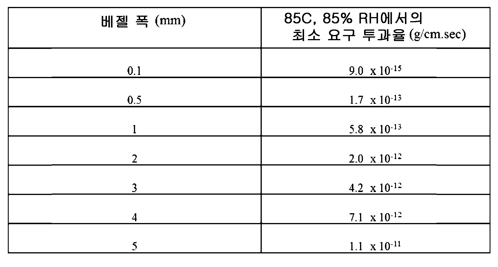
본 발명에 개시된 바와 같은 박막 투과 배리어 시스템의 성능을 실험으로 확인하였다. 모든 실험에서, 하이브리드 배리어층 SiOxCyHz는 산소와 같은 반응성 기체, 예컨대 HMDSO/O2를 이용하는, 유기 전구물질의 플라즈마 촉진형 화학적 증기 증착(PECVD)에 의해 성장시켰다. 박막 투과 배리어의 범용성을 입증하기 위해서, 수개의 무기 배리어층을 다양한 기술에 의해 증착하였으며, 이에는 DC 마그네트론 반응 스퍼터링에 의한 인듐 아연 산화물(IZO), e-빔 증발에 의한 티탄이 포함된다.The performance of the thin film transmission barrier system as disclosed in the present invention was confirmed experimentally. In all experiments, the hybrid barrier layer SiO x C y H z was grown by plasma-enhanced chemical vapor deposition (PECVD) of an organic precursor using a reactive gas such as oxygen, such as HMDSO / O 2 . To demonstrate the versatility of thin film transmission barriers, several inorganic barrier layers were deposited by various techniques including indium zinc oxide (IZO) by DC magnetron reactive sputtering, titanium by e-beam evaporation.
투과 배리어 구조의 평균 응력은 하기 Stoney 수학식을 이용하여 계산할 수 있다:The average stress of the transmission barrier structure can be calculated using the following Stoney equation:

상기 식에서, R은 굴곡 반경이고, E w 는 웨이퍼 탄성 상수이며, h s 는 기판 두께이고, H는 배리어 막 두께이다. 단일층 하이브리드 배리어층이 물에 노출될 경우, H2O가 막으로 확산된다. 그 층이 경질 기판, 예컨대 규소 웨이퍼 또는 경질 유리 상에 증착되는 경우, 배리어는 팽창하는 경향이 있으며, 그 결과 압축 응력이 증가한다. 압축 응력의 변화는 하이브리드 배리어에 용해된 물의 농도(C)에 비례한다:Wherein R, and R is a bend radius, E w is the wafer elastic constant, h s is the substrate thickness, H is the thickness of the barrier film. When the single layer hybrid barrier layer is exposed to water, H 2 O diffuses into the membrane. When the layer is deposited on a rigid substrate, such as a silicon wafer or hard glass, the barrier tends to expand, resulting in increased compressive stress. The change in compressive stress is proportional to the concentration ( C ) of water dissolved in the hybrid barrier:

따라서, 우수한 투과 배리어는 가속된 시험 조건(높은 온도, 높은 상대 습도) 동안에 전반적인 압축 응력에 있어서 최소한의 변화를 가져야 한다. 일부 구체예에서, 하이브리드 배리어 특성은, 다층 배리어 스택 중 탈결합층과 비슷하게 보다 폴리머와 유사한 특성 또는 보다 무기물질과 유사한 특성을 갖도록 본원에 개시된 바와 같이 증착 파라미터들을 변경함으로써 조정할 수 있다. 일반적으로, 폴리머 유사 막은 배리어성이 부족하고, 물에 대한 확산 계수가 더 높으며, 가속화된 시험 조건 하에서 급속한 응력 변화를 보인다.Thus, a good transmission barrier must have a minimum change in overall compressive stress during accelerated test conditions (high temperature, high relative humidity). In some embodiments, the hybrid barrier properties can be adjusted by altering the deposition parameters as described herein to have properties that are more polymer-like or more inorganic than the deblocking layer of the multilayer barrier stack. In general, polymer-like membranes lack barrier properties, have a higher diffusion coefficient for water, and exhibit rapid stress changes under accelerated test conditions.
응력 변화 시험을 수행하기 위해, 미가공 2" Si 웨이퍼를 기판으로서 사용하였다. 500 nm 하이브리드 배리어층을 PECVD에 의해 3가지 웨이퍼(A ∼ C) 각각에 증착시켰다. 이후, 20 nm 두께의 무기 배리어층을 하이브리드 배리어층 위에 증착하였다.A 500 nm hybrid barrier layer was deposited by PECVD on each of the three wafers A to C. Thereafter a 20 nm thick inorganic barrier layer Was deposited on the hybrid barrier layer.
투과 배리어 구조를 하기에 요약한다:The transmission barrier structure is summarized below:
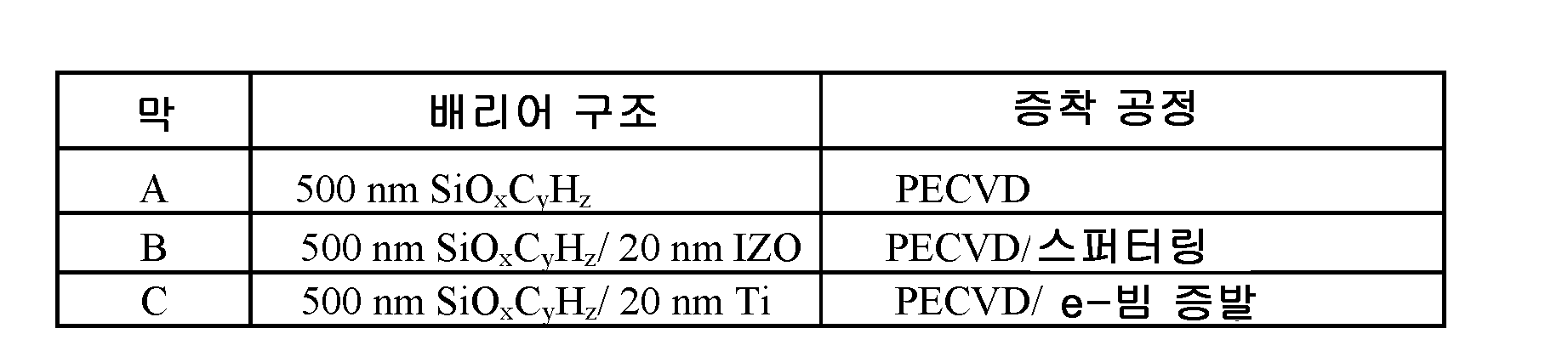
샘플들의 평균 응력은 85C, 85% 상대 습도(RH)에서 경시적으로 모니터링하였다. 도 12는 85C/85% RH에서의 시간의 함수로서의 응력 변화의 플롯을 도시한다. 삽화는 테스트의 처음 24 시간 동안에 동일함을 보인다. 도시된 바와 같이, 단일 하이브리드 배리어(막 A)의 응력은, 85C, 85% RH에서 6 시간 내에 -75.7 MPa(압축)까지 급속히 변화한다. 막 A가 물에 노출될 경우, H2O가 막으로 확산되면서, 막을 팽창시키며, 그 결과로 압축 응력이 증가한다. 압축 응력의 변화(즉, 보다 음의 값)는 배리어에 용해된 물의 농도와 직접 관련된다. 앞서 언급한 바와 같이, 이 층의 특성은, 상대적으로 부족한 배리어인 폴리머 유사 막을 증착하기 위해 변경하였다. 이러한 폴리머 유사 막의 응력 변화는 매우 급속하게, 예를 들어 2 시간 이하로 일어날 수 있다. 막 B 및 C 각각의 응력 변화는 504 시간 후에도 경미하다. 또한, 응력은 막 B에 있어서는 504 시간 후 그의 최대 값인 -54 MPa(압축)으로, 그리고 막 C에 있어서는 456 시간 후 +19 MPa로 변화하였다. 이 비교적 낮은 응력 변화 속도는, 무기층이 하이브리드층을 "차폐한다"는 이론과 일치한다. 환경 시험 조건 하에서, 무기 차폐층/하이브리드 배리어층 경계에 이르는 수증기의 플럭스는 무기층 중 결함부 크기 및 밀도가 우세하다. 이어서, 이 "편재화된" 물 분자들은 하이브리드 배리어층을 3차원적으로 투과한다.The average stress of the samples was monitored over time at 85 C, 85% relative humidity (RH). Figure 12 shows a plot of stress variation as a function of time at 85 C / 85% RH. The illustrations show the same during the first 24 hours of the test. As shown, the stresses of the single hybrid barrier (film A) change rapidly at 85 C, 85% RH to -75.7 MPa (compression) within 6 hours. When membrane A is exposed to water, H 2 O diffuses into the membrane, causing the membrane to expand, resulting in increased compressive stress. The change in compressive stress (i.e., the more negative value) is directly related to the concentration of water dissolved in the barrier. As noted above, the properties of this layer have been modified to deposit a polymer-like film that is a relatively poor barrier. The stress variation of such a polymer-like membrane can occur very rapidly, for example up to 2 hours. The stress change of each of the films B and C is also slight after 504 hours. In addition, the stress was changed to -54 MPa (compression), which is its maximum value after 504 hours in film B, and to +19 MPa, in film C, after 456 hours. This relatively low stress change rate is consistent with the theory that the inorganic layer "shields " the hybrid layer. Under environmental test conditions, the flux of water vapor reaching the inorganic shielding layer / hybrid barrier layer boundary is predominant in defect size and density in the inorganic layer. These "shunted" water molecules then transmit the hybrid barrier layer three-dimensionally.
OLED의 캡슐화를 시험하기 위해서, 유효 면적이 2 mm2이고 감습 Mg:Ag 캐소드를 지닌 투명한 OLED 디바이스를 유리 기판에 성장시킨 후, 이하에 열거한 바와 같이 박막 배리어로 캡슐화하였다:To test the encapsulation of the OLED, a transparent OLED device with an effective area of 2 mm 2 and a humid Mg: Ag cathode was grown on a glass substrate and then encapsulated in a thin film barrier as listed below:
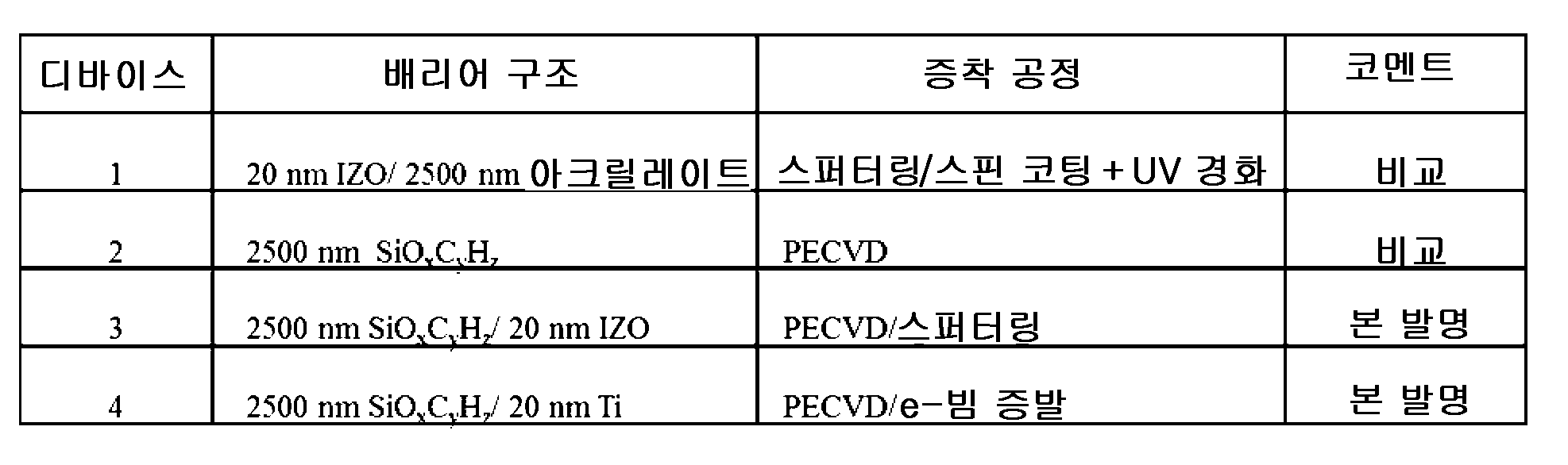
이어서, 디바이스를, 비교적 부족한 배리어로 여겨지는 스크래치 보호용 고분자층으로 코팅하였다. 그 디바이스를 85C, 85% 상대 습도(RH)에서 경시적으로 모니터링하였다. 도 13∼16은 85C/85% RH에서의 에이징 전후의 OLED 디바이스의 사진을 도시한다. 제1 비교 디바이스, 디바이스 1(20 nm IZO + 2500 nm 아크릴레이트)은 도 13에 도시된 바와 같이, 24 시간 후에 다수의 흑점 성장을 보였다. 이는 IZO 층 내의 핀 홀 또는 다른 결함부를 통한 수증기 확산에 기인하는 것으로 보인다. 이 디바이스 내의 유효 면적은 24 시간 내에 1% 초과로 수축하였다. 제2 비교 디바이스, 디바이스 2(2500 nm SiOxCyHz)는 결함부를 포함하지 않았고, 도 14에 도시된 바와 같이 96 시간까지 균일하게 빛났으며, 그 후, 100 시간 후에는 치명적으로 발광하지 못하였다. 이는 배리어를 통한 수증기의 대량 투과로 인한 Mg:Ag 캐소드의 완전 산화에 기인하는 것으로 보인다. 본원에 개시된 구체예에 따라 제조된 디바이스 3(2500 nm SiOxCyHz / 20 nm IZO)는 500 시간 후에도 온전히 유지되었으며, 도 15에 도시된 바와 같이 흑점 성장의 조짐을 보이지 않았다. 본원에 개시된 구체예에 따라 제조된 디바이스 4(2500 nm SiOxCyHz / 20 nm Ti)는, 유사한 거동을 보였으며, 도 16에 도시된 바와 같이 흑점 성장의 조짐을 보이지 않았다. 따라서, 본원에 개시된 구체예에 따른 디바이스는 85C, 85% RH에서 500 시간 후에 유효 면적의 소실을 나타내지 않는 것으로 확인되었다.The device was then coated with a polymer layer for scratch protection, which is considered a relatively deficient barrier. The device was monitored over time at 85 C, 85% relative humidity (RH). Figures 13-16 show photographs of OLED devices before and after aging at 85C / 85% RH. The first comparison device, Device 1 (20 nm IZO + 2500 nm acrylate) showed a large number of black spot growth after 24 hours, as shown in Fig. This appears to be due to water vapor diffusion through pinholes or other defects in the IZO layer. The effective area within this device shrank by more than 1% within 24 hours. The second comparison device, Device 2 (2500 nm SiO x C y H z ), did not contain any defects and was uniformly lit up to 96 hours as shown in Figure 14, and then fired after 100 hours I did not. This seems to be due to the complete oxidation of the Mg: Ag cathode due to the mass permeation of water vapor through the barrier. The device 3 (2500 nm SiO x C y H z / 20 nm IZO) prepared according to embodiments disclosed herein was maintained intact even after 500 hours and showed no sign of black spot growth as shown in FIG. The device 4 (2500 nm SiO x C y H z / 20 nm Ti) produced according to embodiments disclosed herein showed similar behavior and did not show signs of black spot growth as shown in FIG. Thus, devices according to the embodiments disclosed herein were found not to exhibit loss of effective area after 85 hours at 85 C, 85% RH.
본원에 개시된 바와 같은 디바이스의 가요성을 시험하기 위해서, 2" × 3"의 50 ㎛ 두께의 PEN 시트를, 본원에 개시된 바와 같은 박막 투과 배리어 구조로 코팅하였다. 배리어 코팅된 PEN을 1.27 cm 반경에 걸쳐서 10,000 사이클 동안 롤링함으로써 가요성을 시험하였다. 배리어는, 임의의 균열 없이 이 시험을 통과할 경우에 가요성인 것으로 간주될 수 있다. 다양한 투과 배리어 구조의 가요성 시험 결과를 하기 표에 열거한다:In order to test the flexibility of the device as disclosed herein, a 2 "x 3" 50 um thick PEN sheet was coated with a thin film transmission barrier structure as disclosed herein. The flexibility was tested by rolling barrier coated PEN over a 1.27 cm radius for 10,000 cycles. Barriers can be considered to be flexible if they pass this test without any cracks. Flexibility test results of various transmission barrier structures are listed in the following table:

나타낸 바와 같이, 본원에 개시된 바와 같은 디바이스는 균열을 나타내지 않고 시험을 통과할 수 있음을 확인하였다.As shown, it has been found that devices as disclosed herein can pass the test without exhibiting cracks.
본원에 기술된 다양한 구체예는 단지 예시이며, 본 발명의 범위를 제한하려는 것이 아님을 이해해야 한다. 예를 들면, 본원에 기술된 많은 물질 및 구조는 본 발명의 취지에서 벗어나는 일 없이 다른 물질 및 구조로 대체될 수 있다. 따라서, 청구된 본 발명은 당업자가 알 수 있는 바와 같이 본원에 기술된 특정예 및 바람직한 구체예로부터의 변형을 포함할 수 있다. 본 발명이 작용하는 이유와 관련한 다양한 이론은 한정하고자 하는 것이 아님을 이해하여야 한다.It should be understood that the various embodiments described herein are illustrative only and are not intended to limit the scope of the invention. For example, many of the materials and structures described herein may be substituted with other materials and structures without departing from the spirit of the invention. Accordingly, the claimed invention may include variations from the specific examples and preferred embodiments described herein as will be appreciated by those skilled in the art. It is to be understood that the various Theories relating to the reason why the present invention operates are not intended to be limiting.
Claims (20)
SiOxCyHz(여기서, 1 ≤ x < 2이고, 0.001 ≤ y ≤ 1이며, 0.001 ≤ z ≤ 1임)를 포함하는 제1 하이브리드 배리어층; 및
제1 하이브리드 배리어층에 바로 인접하게 배치되는 무기(inorganic) 제2 배리어층
을 포함하는 박막 배리어.As a thin film barrier,
A first hybrid barrier layer comprising SiO x C y H z wherein 1 ≤ x <2, 0.001 ≤ y ≤ 1, and 0.001 ≤ z ≤ 1; And
An inorganic second barrier layer disposed immediately adjacent to the first hybrid barrier layer,
/ RTI >
하나 이상의 전구물질 각각을 플라즈마 증착하여, 기판 위에 SiOxCyHz를 포함하는 배리어층을 형성시키는 단계; 및
배리어층에 바로 인접하게, 기판 위에 무기층을 증착하는 단계
를 포함하는 방법.Obtaining at least one precursor, wherein at least one precursor comprises at least one organosilicon precursor;
Plasma-depositing each of the one or more precursors to form a barrier layer comprising SiO x C y H z on the substrate; And
Depositing an inorganic layer on the substrate immediately adjacent to the barrier layer,
≪ / RTI >
Applications Claiming Priority (2)
| Application Number | Priority Date | Filing Date | Title |
|---|---|---|---|
| US14/464,997 US20160056414A1 (en) | 2014-08-21 | 2014-08-21 | Thin film permeation barrier system for substrates and devices and method of making the same |
| US14/464,997 | 2014-08-21 |
Publications (2)
| Publication Number | Publication Date |
|---|---|
| KR20160028362A true KR20160028362A (en) | 2016-03-11 |
| KR102321945B1 KR102321945B1 (en) | 2021-11-04 |
Family
ID=55349036
Family Applications (1)
| Application Number | Title | Priority Date | Filing Date |
|---|---|---|---|
| KR1020150117982A Active KR102321945B1 (en) | 2014-08-21 | 2015-08-21 | Thin film permeation barrier system for substrates and devices and method of making the same |
Country Status (3)
| Country | Link |
|---|---|
| US (1) | US20160056414A1 (en) |
| KR (1) | KR102321945B1 (en) |
| CN (2) | CN105390621A (en) |
Cited By (1)
| Publication number | Priority date | Publication date | Assignee | Title |
|---|---|---|---|---|
| KR20190117621A (en) * | 2017-03-29 | 2019-10-16 | 데이진 가부시키가이샤 | Polymer substrate with hard coat layer |
Families Citing this family (12)
| Publication number | Priority date | Publication date | Assignee | Title |
|---|---|---|---|---|
| KR20150109984A (en) * | 2014-03-21 | 2015-10-02 | 삼성전자주식회사 | Gas barrier film, refrigerator having the same and method of manufacturing the gas barrier film |
| WO2016190855A1 (en) * | 2015-05-27 | 2016-12-01 | Hewlett-Packard Development Company, L.P. | Articles having flexible substrates |
| KR102330331B1 (en) * | 2015-07-17 | 2021-11-25 | 삼성디스플레이 주식회사 | Organic luminescence emitting display device and the method of manufacturing the same |
| KR102402606B1 (en) * | 2015-10-19 | 2022-05-27 | 삼성디스플레이 주식회사 | Flexible display apparatus and manufacturing method thereof |
| CN105655494B (en) * | 2016-03-18 | 2018-08-24 | 深圳市华星光电技术有限公司 | Substrate of Organic Light Emitting Diode and preparation method thereof, Organic Light Emitting Diode |
| US10483489B2 (en) * | 2016-08-12 | 2019-11-19 | Universal Display Corporation | Integrated circular polarizer and permeation barrier for flexible OLEDs |
| US11751426B2 (en) * | 2016-10-18 | 2023-09-05 | Universal Display Corporation | Hybrid thin film permeation barrier and method of making the same |
| WO2018130300A1 (en) * | 2017-01-13 | 2018-07-19 | Applied Materials, Inc. | Layer system adapted for use in an electro-optical device and method for manufacturing a layer system in a continuous roll-to-roll process |
| US11569447B2 (en) * | 2019-08-26 | 2023-01-31 | Wuhan China Star Optoelectronics Semiconductor Display Technology Co., Ltd. | Method for testing performance of thin-film encapsulation |
| US11362307B2 (en) | 2019-11-27 | 2022-06-14 | Applied Materials, Inc. | Encapsulation having polymer and dielectric layers for electronic displays |
| US11258045B2 (en) | 2019-11-27 | 2022-02-22 | Applied Materials, Inc. | Methods of forming stretchable encapsulation for electronic displays |
| US11211439B2 (en) | 2019-11-27 | 2021-12-28 | Applied Materials, Inc. | Stretchable polymer and dielectric layers for electronic displays |
Citations (5)
| Publication number | Priority date | Publication date | Assignee | Title |
|---|---|---|---|---|
| JP2003535939A (en) * | 2000-06-06 | 2003-12-02 | ザ ダウ ケミカル カンパニー | Permeable barrier layers for polymers and containers |
| KR20050104401A (en) * | 2003-02-26 | 2005-11-02 | 다우 코닝 코포레이션 | Method for producing hydrogenated silicon oxycarbide films |
| US20070020451A1 (en) * | 2005-07-20 | 2007-01-25 | 3M Innovative Properties Company | Moisture barrier coatings |
| CN103258955A (en) * | 2012-02-20 | 2013-08-21 | 中国科学院微电子研究所 | Encapsulation methods for organic electronic devices |
| US20150159271A1 (en) * | 2013-12-09 | 2015-06-11 | Veeco Ald Inc. | Deposition of non-isostructural layers for flexible substrate |
Family Cites Families (11)
| Publication number | Priority date | Publication date | Assignee | Title |
|---|---|---|---|---|
| US6492026B1 (en) * | 2000-04-20 | 2002-12-10 | Battelle Memorial Institute | Smoothing and barrier layers on high Tg substrates |
| US20070054149A1 (en) * | 2005-08-23 | 2007-03-08 | Chi-Ming Cheng | Substrate assembly of a display device and method of manufacturing the same |
| US7767498B2 (en) * | 2005-08-25 | 2010-08-03 | Vitex Systems, Inc. | Encapsulated devices and method of making |
| US7621794B2 (en) * | 2005-11-09 | 2009-11-24 | International Display Systems, Inc. | Method of encapsulating an organic light-emitting device |
| US20080006819A1 (en) * | 2006-06-19 | 2008-01-10 | 3M Innovative Properties Company | Moisture barrier coatings for organic light emitting diode devices |
| CN101668879B (en) * | 2007-03-28 | 2012-05-09 | 陶氏康宁公司 | Roll-to-roll plasma-enhanced chemical vapor deposition method for barrier layers containing silicon and carbon |
| JP5470969B2 (en) * | 2009-03-30 | 2014-04-16 | 株式会社マテリアルデザインファクトリ− | Gas barrier film, electronic device including the same, gas barrier bag, and gas barrier film manufacturing method |
| KR101718560B1 (en) * | 2009-04-09 | 2017-03-21 | 스미또모 가가꾸 가부시키가이샤 | Gas-barrier multilayer film |
| US8753711B2 (en) * | 2009-12-18 | 2014-06-17 | General Electric Company | Edge sealing method using barrier coatings |
| US20130236681A1 (en) * | 2012-03-06 | 2013-09-12 | Chang Min Lee | Photocurable composition, barrier layer including the same, and encapsulated apparatus including the same |
| CN103943789A (en) * | 2014-04-18 | 2014-07-23 | 深圳市华星光电技术有限公司 | OLED device and manufacturing method thereof |
-
2014
- 2014-08-21 US US14/464,997 patent/US20160056414A1/en not_active Abandoned
-
2015
- 2015-08-19 CN CN201510511427.2A patent/CN105390621A/en active Pending
- 2015-08-19 CN CN202010661902.5A patent/CN111769206A/en active Pending
- 2015-08-21 KR KR1020150117982A patent/KR102321945B1/en active Active
Patent Citations (5)
| Publication number | Priority date | Publication date | Assignee | Title |
|---|---|---|---|---|
| JP2003535939A (en) * | 2000-06-06 | 2003-12-02 | ザ ダウ ケミカル カンパニー | Permeable barrier layers for polymers and containers |
| KR20050104401A (en) * | 2003-02-26 | 2005-11-02 | 다우 코닝 코포레이션 | Method for producing hydrogenated silicon oxycarbide films |
| US20070020451A1 (en) * | 2005-07-20 | 2007-01-25 | 3M Innovative Properties Company | Moisture barrier coatings |
| CN103258955A (en) * | 2012-02-20 | 2013-08-21 | 中国科学院微电子研究所 | Encapsulation methods for organic electronic devices |
| US20150159271A1 (en) * | 2013-12-09 | 2015-06-11 | Veeco Ald Inc. | Deposition of non-isostructural layers for flexible substrate |
Cited By (1)
| Publication number | Priority date | Publication date | Assignee | Title |
|---|---|---|---|---|
| KR20190117621A (en) * | 2017-03-29 | 2019-10-16 | 데이진 가부시키가이샤 | Polymer substrate with hard coat layer |
Also Published As
| Publication number | Publication date |
|---|---|
| US20160056414A1 (en) | 2016-02-25 |
| KR102321945B1 (en) | 2021-11-04 |
| CN105390621A (en) | 2016-03-09 |
| CN111769206A (en) | 2020-10-13 |
Similar Documents
| Publication | Publication Date | Title |
|---|---|---|
| KR102321945B1 (en) | Thin film permeation barrier system for substrates and devices and method of making the same | |
| US12446451B2 (en) | Electronic device with reduced non-device edge area | |
| KR102211205B1 (en) | Edge barrier film for electronic devices | |
| US20160254487A1 (en) | Permeation barrier system for substrates and devices and method of making the same | |
| US20190221771A1 (en) | Buffer layer for organic light emitting devices and method of making the same | |
| US20160118621A1 (en) | Hybrid barrier layer for substrates and electronic devices | |
| US11665951B2 (en) | Barrier film for electronic devices and substrates |
Legal Events
| Date | Code | Title | Description |
|---|---|---|---|
| PA0109 | Patent application |
St.27 status event code: A-0-1-A10-A12-nap-PA0109 |
|
| P22-X000 | Classification modified |
St.27 status event code: A-2-2-P10-P22-nap-X000 |
|
| PG1501 | Laying open of application |
St.27 status event code: A-1-1-Q10-Q12-nap-PG1501 |
|
| P22-X000 | Classification modified |
St.27 status event code: A-2-2-P10-P22-nap-X000 |
|
| A201 | Request for examination | ||
| PA0201 | Request for examination |
St.27 status event code: A-1-2-D10-D11-exm-PA0201 |
|
| E902 | Notification of reason for refusal | ||
| PE0902 | Notice of grounds for rejection |
St.27 status event code: A-1-2-D10-D21-exm-PE0902 |
|
| E13-X000 | Pre-grant limitation requested |
St.27 status event code: A-2-3-E10-E13-lim-X000 |
|
| P11-X000 | Amendment of application requested |
St.27 status event code: A-2-2-P10-P11-nap-X000 |
|
| P13-X000 | Application amended |
St.27 status event code: A-2-2-P10-P13-nap-X000 |
|
| E701 | Decision to grant or registration of patent right | ||
| PE0701 | Decision of registration |
St.27 status event code: A-1-2-D10-D22-exm-PE0701 |
|
| GRNT | Written decision to grant | ||
| PR0701 | Registration of establishment |
St.27 status event code: A-2-4-F10-F11-exm-PR0701 |
|
| PR1002 | Payment of registration fee |
St.27 status event code: A-2-2-U10-U11-oth-PR1002 Fee payment year number: 1 |
|
| PG1601 | Publication of registration |
St.27 status event code: A-4-4-Q10-Q13-nap-PG1601 |
|
| R18-X000 | Changes to party contact information recorded |
St.27 status event code: A-5-5-R10-R18-oth-X000 |
|
| P22-X000 | Classification modified |
St.27 status event code: A-4-4-P10-P22-nap-X000 |
|
| P22-X000 | Classification modified |
St.27 status event code: A-4-4-P10-P22-nap-X000 |
|
| P22-X000 | Classification modified |
St.27 status event code: A-4-4-P10-P22-nap-X000 |
|
| PR1001 | Payment of annual fee |
St.27 status event code: A-4-4-U10-U11-oth-PR1001 Fee payment year number: 4 |
|
| P22-X000 | Classification modified |
St.27 status event code: A-4-4-P10-P22-nap-X000 |
|
| P22-X000 | Classification modified |
St.27 status event code: A-4-4-P10-P22-nap-X000 |