KR20150135202A - Perovskite schottky type solar cell - Google Patents
Perovskite schottky type solar cell Download PDFInfo
- Publication number
- KR20150135202A KR20150135202A KR1020157018975A KR20157018975A KR20150135202A KR 20150135202 A KR20150135202 A KR 20150135202A KR 1020157018975 A KR1020157018975 A KR 1020157018975A KR 20157018975 A KR20157018975 A KR 20157018975A KR 20150135202 A KR20150135202 A KR 20150135202A
- Authority
- KR
- South Korea
- Prior art keywords
- layer
- perovskite
- substrate
- member according
- group
- Prior art date
Links
Images


Classifications
-
- H—ELECTRICITY
- H10—SEMICONDUCTOR DEVICES; ELECTRIC SOLID-STATE DEVICES NOT OTHERWISE PROVIDED FOR
- H10K—ORGANIC ELECTRIC SOLID-STATE DEVICES
- H10K30/00—Organic devices sensitive to infrared radiation, light, electromagnetic radiation of shorter wavelength or corpuscular radiation
- H10K30/10—Organic devices sensitive to infrared radiation, light, electromagnetic radiation of shorter wavelength or corpuscular radiation comprising heterojunctions between organic semiconductors and inorganic semiconductors
- H10K30/15—Sensitised wide-bandgap semiconductor devices, e.g. dye-sensitised TiO2
- H10K30/151—Sensitised wide-bandgap semiconductor devices, e.g. dye-sensitised TiO2 the wide bandgap semiconductor comprising titanium oxide, e.g. TiO2
-
- H01L51/4226—
-
- H01L51/0036—
-
- H—ELECTRICITY
- H10—SEMICONDUCTOR DEVICES; ELECTRIC SOLID-STATE DEVICES NOT OTHERWISE PROVIDED FOR
- H10K—ORGANIC ELECTRIC SOLID-STATE DEVICES
- H10K85/00—Organic materials used in the body or electrodes of devices covered by this subclass
-
- H—ELECTRICITY
- H10—SEMICONDUCTOR DEVICES; ELECTRIC SOLID-STATE DEVICES NOT OTHERWISE PROVIDED FOR
- H10K—ORGANIC ELECTRIC SOLID-STATE DEVICES
- H10K85/00—Organic materials used in the body or electrodes of devices covered by this subclass
- H10K85/30—Coordination compounds
-
- H—ELECTRICITY
- H10—SEMICONDUCTOR DEVICES; ELECTRIC SOLID-STATE DEVICES NOT OTHERWISE PROVIDED FOR
- H10K—ORGANIC ELECTRIC SOLID-STATE DEVICES
- H10K85/00—Organic materials used in the body or electrodes of devices covered by this subclass
- H10K85/50—Organic perovskites; Hybrid organic-inorganic perovskites [HOIP], e.g. CH3NH3PbI3
-
- H01L2251/306—
-
- H—ELECTRICITY
- H10—SEMICONDUCTOR DEVICES; ELECTRIC SOLID-STATE DEVICES NOT OTHERWISE PROVIDED FOR
- H10K—ORGANIC ELECTRIC SOLID-STATE DEVICES
- H10K2102/00—Constructional details relating to the organic devices covered by this subclass
- H10K2102/10—Transparent electrodes, e.g. using graphene
- H10K2102/101—Transparent electrodes, e.g. using graphene comprising transparent conductive oxides [TCO]
- H10K2102/102—Transparent electrodes, e.g. using graphene comprising transparent conductive oxides [TCO] comprising tin oxides, e.g. fluorine-doped SnO2
-
- H—ELECTRICITY
- H10—SEMICONDUCTOR DEVICES; ELECTRIC SOLID-STATE DEVICES NOT OTHERWISE PROVIDED FOR
- H10K—ORGANIC ELECTRIC SOLID-STATE DEVICES
- H10K85/00—Organic materials used in the body or electrodes of devices covered by this subclass
- H10K85/10—Organic polymers or oligomers
- H10K85/111—Organic polymers or oligomers comprising aromatic, heteroaromatic, or aryl chains, e.g. polyaniline, polyphenylene or polyphenylene vinylene
- H10K85/113—Heteroaromatic compounds comprising sulfur or selene, e.g. polythiophene
-
- Y—GENERAL TAGGING OF NEW TECHNOLOGICAL DEVELOPMENTS; GENERAL TAGGING OF CROSS-SECTIONAL TECHNOLOGIES SPANNING OVER SEVERAL SECTIONS OF THE IPC; TECHNICAL SUBJECTS COVERED BY FORMER USPC CROSS-REFERENCE ART COLLECTIONS [XRACs] AND DIGESTS
- Y02—TECHNOLOGIES OR APPLICATIONS FOR MITIGATION OR ADAPTATION AGAINST CLIMATE CHANGE
- Y02E—REDUCTION OF GREENHOUSE GAS [GHG] EMISSIONS, RELATED TO ENERGY GENERATION, TRANSMISSION OR DISTRIBUTION
- Y02E10/00—Energy generation through renewable energy sources
- Y02E10/50—Photovoltaic [PV] energy
- Y02E10/549—Organic PV cells
Abstract
본 발명은 지지 구조체 층이 없는 광전지와 같은 장치를 제공한다.The present invention provides an apparatus, such as a photovoltaic cell, without a support structure layer.
Description
본 발명은 일반적으로 새로운 타입의 태양 전지에 관한 것이다.The present invention relates generally to new types of solar cells.
유무기 페로브스카이트는 태양 전지에서 광 회수 장치로 사용하기에 매력적인 물질이다. 태양 전지에 사용하기에 유망한 유무기 페로브스카이트는 유기 할로젠화 납 페로브스카이트이다. 유기 할로젠화 납 페로브스카이트는 직접 천이 밴드 갭, 큰 흡수 계수[1,2], 및 높은 캐리어 이동도[3]를 가진다. 유기 할로젠화 납 페로브스카이트의 전기적 특성은, 층상 물질의 형성을 가능케 하면서, 사용된 유기 구성요소의 구조에 따라 무기 시트들 간의 거리 및 전자 결합을 제어하도록 조정될 수 있다. 층상 페로브스카이트는 건조 공기 중에서 안정성이 높다.The presence or absence of perovskite is an attractive material for use as a light recovery device in solar cells. Perovskite, which is promising for use in solar cells, is an organic halogenated perovskite. Organohalogenated lead perovskites have direct transition bandgaps, large absorption coefficients [1,2], and high carrier mobility [3]. The electrical properties of the organohalogenated lead perovskite can be adjusted to control the distance between the inorganic sheets and the electronic coupling, depending on the structure of the organic component used, allowing for the formation of layered materials. Layered perovskite has high stability in dry air.
몇몇 연구들은 액체 전해질을 지닌 광전자 화학 전지에서 감응제로서 CH3NH3PbI3 페로브스카이트 나노 결정을 사용하는 것에 대해 보고하고 있다[4-6]. 그러나, 이러한 시스템의 성능은 페로브스카이트의 용출로 인해 급격히 감소한다.Several studies have reported using CH 3 NH 3 PbI 3 perovskite nanocrystals as sensitizers in photoelectrochemical cells with liquid electrolytes [4-6]. However, the performance of such a system is drastically reduced due to the elution of perovskite.
Snaith 등[7] 및 Graetzel 등[8]은 미소-초구조체로 된 유기 할로젠화물 페로브스카이트를 기반으로, 전력 변환 효율이 10 %를 초과하는 효율적인 유무기 복합 태양 전지에 관해 보고하였다.Snaith et al. [7] and Graetzel et al. [8] reported efficient organic-inorganic hybrid solar cells with power conversion efficiencies exceeding 10% based on organic halide perovskite with micro-superstructure.
또한, Etgar 등[9]은 정공 전도체가 없는 페로브스카이트 이종접합 태양 전지의 사용에 관해 보고하였다. 이 저자들은 할로젠화 납 페로브스카이트가, 흡수체로서의 기능뿐만 아니라 낮은 광도 하에서 전력 변환 효율이 7 %를 초과하는 우수한 광전지 성능을 달성하면서, 정공을 전달할 수 있다는 것을 밝혀냈다. Etgar 등은 또한 γ-부티롤락톤 내의 CH3NH3I 및 PbI2 용액으로부터 얻어진 페로브스카이트 나노 입자들을 400 nm 두께의 TiO2 (예추석) 나노 시트 필름 상에 증착함으로써 만들어진, 미소 메틸암모늄 아이오딘화 납 (CH3NH3PbI3) 페로브스카이트/TiO2를 포함하는 미소 CH3NH3PbI3/TiO2 이종접합 태양 전지를 개시하고 있다. 이 저자들이 주장하는 바에 따라 주로 표면적을 증가시키기 위해 지지체(scaffold)로써 TiO2가 필요하므로 TiO2의 존재는 결정적인 것으로 밝혀졌다.Etgar et al. [9] also reported the use of perovskite heterojunction solar cells without a hole conductor. These authors have found that halogenated lead perovskite can deliver holes as well as function as an absorber, while achieving excellent photovoltaic performance in excess of 7% power conversion efficiency under low light intensity. Etgar et al. Also incorporated perovskite nanoparticles obtained from CH 3 NH 3 I and PbI 2 solutions in? -Butyrolactone onto a 400 nm thick TiO 2 iodine Chemistry lead (CH 3 NH 3 PbI 3) discloses a perovskite / TiO 2 minute CH 3 NH 3 PbI 3 / TiO 2 heterojunction solar cell comprising a. The authors have found that the presence of TiO 2 is crucial because it requires TiO 2 as a scaffold to increase the surface area.
유무기 페로브스카이트를 기반으로 한 현재 공지된 태양 전지 또는 이종접합체는 그러한 전지에서 중요한 구성요소로 간주되는 지지체 층(예컨대 TiO2층)을 이용한다. 지지체 층은 일반적으로 페로브스카이트 층과 유리 기판 사이에 위치한다. 이는 지지체 층이 표면적을 증가시키고 그로 인해 재결합 과정을 줄이거나 약화시키는데 도움을 줌으로써 장치 효율을 증가시킨다는 사실에 주로 기인한다.Presently known solar cells or heterogeneous junctions based on organic or inorganic perovskites use a support layer (e.g. a TiO 2 layer) which is regarded as an important component in such a cell. The support layer is generally located between the perovskite layer and the glass substrate. This is mainly due to the fact that the support layer increases the device efficiency by increasing the surface area and thereby helping to reduce or attenuate the recombination process.
본 발명은 태양 전지에서 표면적을 증가시키는 지지 구조체 층을 포함시킬 필요 없이 페로브스카이트 물질들로부터 효율적인 페로브스카이트 태양 전지를 만들 수 있다는 놀라운 발견에 기반을 두고 있다.The present invention is based on the surprising discovery that an efficient perovskite solar cell can be made from perovskite materials without the need to include a support structure layer that increases the surface area in solar cells.
따라서, 본 발명의 목적은 표면적을 증가시키는 지지 구조체/층이 없는 광전자 장치에서 이용될 수 있는 새로운 적층체(stacked layer) 부재를 제공하는 데 있다. 이러한 장치는 개선된 광전자 장치/이종접합체/광전지이다. 본 발명의 적층체는, 이하에서 더 설명되는 바와 같이, 다음과 같은 하나 이상의 특징을 나타낸다.It is therefore an object of the present invention to provide a novel stacked layer member which can be used in an optoelectronic device without a support structure / layer that increases the surface area. Such devices are improved optoelectronic devices / heterozygotes / photovoltaic cells. The laminate of the present invention exhibits one or more of the following characteristics, as described further below.
1. 적층체는 구조가 간단하며, 표면적을 증가시키는 지지체 구성요소의 제거 결과에 따라 비용 효율적이고 용이하게 구성할 수 있는 장치를 구성할 수 있도록 한다.1. The laminate is simple in structure and makes it possible to constitute a device that is cost effective and easy to configure according to the result of removal of the support component which increases the surface area.
2. 저온에서 그리고/또는 간단한 증착 단계(들)로 적층체를 형성하면, 표면적을 증가시키는 지지 구조체를 적용하지 않아도 되는 공정으로 인해, 비용 효율적인 장치를 제공한다.2. The formation of a laminate at low temperature and / or in a simple deposition step (s) provides a cost effective device due to the process which does not require the application of support structures to increase the surface area.
3. 따라서, 가용성 기판 및/또는 감열성 표면 상에 증착되고/되거나 가요성인 적층체는 사용될 수 있는 기판의 선택 및 최종 응용의 범위를 넓힌다.3. Thus, the laminate deposited and / or flexible on the soluble substrate and / or the thermally sensitive surface broadens the selection and final application of the substrate that can be used.
4. 이종접합체/광전지/장치의 공핍층이 표면에 매우 가깝기 때문에, 적층체는 전하 캐리어 재결합 영향을 덜 받는다.4. Because the depletion layer of the heterojunction / photovoltaic device / device is very close to the surface, the stack is less affected by charge carrier recombination.
5. 적층체는 전류 밀도가 높은 장치를 제공한다.5. The laminate provides a device with high current density.
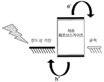
따라서, 본 발명은 일 양태에서, 기판, 적어도 하나의 (예컨대, 유무기) 페로브스카이트 층, 전도층, 및 선택적인 적어도 하나의 추가 층을 포함하는(또는 이들로 이루어진) 부재로서, 적어도 하나의 페로브스카이트 층은, 기판 상에 직접 또는 상기 기판 상에 위치한 적어도 하나의 추가 층 상에서, 상기 기판 상에 제공되고, 상기 적어도 하나의 추가 층은 지지 구조체 층과 다른, 부재를 제공한다.Accordingly, in one aspect, the present invention provides a member comprising (or consisting of) a substrate, at least one (e.g., an organic) perovskite layer, a conducting layer, and optionally at least one additional layer, One perovskite layer is provided on the substrate, either directly on the substrate or on at least one additional layer located on the substrate, the at least one additional layer providing a member different from the support structure layer .
일부 실시예들에서, 기판은 그 상단에 페로브스카이트 층이 제공되는 최하단 층이며, 페로브스카이트 층의 상단에 전도층이 제공된다. 지지 구조체 층이 아닌 적어도 하나의 추가 층은 전술한 기판, 페로브스카이트, 및 전도층 중 어느 하나 사이의 개재층일 수 있거나, 또는 상기 전도층의 상단에 있는 최상단 층일 수 있다.In some embodiments, the substrate is the bottom layer where a perovskite layer is provided at the top thereof, and a conductive layer is provided at the top of the perovskite layer. At least one additional layer other than the support structure layer may be an intervening layer between any of the above-described substrate, perovskite, and conductive layer, or may be the top layer at the top of the conductive layer.
본 발명은 또한 기판, 적어도 하나의 페로브스카이트 층, 전도층, 및 선택적인 적어도 하나의 추가 층을 포함하는 부재로서, 지지 구조체 층이 결여된(또는 없는) 부재를 제공한다.The present invention also provides a member that includes a substrate, at least one perovskite layer, a conductive layer, and at least one optional additional layer, wherein the support structure layer is absent (or absent).
본 발명은 또한 기판, 적어도 하나의 페로브스카이트 층, 전도층, 선택적인 적어도 하나의 추가 층, 및 추가로 선택적인 적어도 하나의 지지 구조체 층을 포함하는 부재로서, 페로브스카이트 층이 상기 기판 상에 직접 제공되는, 부재를 제공한다.The present invention also relates to a member comprising a substrate, at least one perovskite layer, a conducting layer, at least one additional optional layer, and at least one further optional support layer, wherein the perovskite layer comprises And is provided directly on the substrate.
본 발명은 또한 기판, 적어도 하나의 페로브스카이트 층, 전도층, 및 선택적인 적어도 하나의 추가 층을 포함하는 부재로서, 상기 기판 상의 적어도 하나의 페로브스카이트 층이 평면 접합을 제공하는, 부재를 제공한다. 즉 지지 구조체 층이 기판과 페로브스카이트 층 사이에 제공되지 않는다.The present invention also relates to a member comprising a substrate, at least one perovskite layer, a conducting layer, and at least one additional optional layer, wherein at least one perovskite layer on the substrate provides planar bonding, Member. A support structure layer is not provided between the substrate and the perovskite layer.
본 발명은 또한 기판, 적어도 하나의 페로브스카이트 층, 전도층, 및 선택적인 적어도 하나의 추가 층을 포함하는 부재로서, 적어도 하나의 페로브스카이트 층이 상기 기판 상에 직접 위치하는, 부재를 제공한다.The present invention also relates to a member comprising a substrate, at least one perovskite layer, a conducting layer, and optionally at least one additional layer, wherein at least one perovskite layer is located directly on the substrate, Lt; / RTI >
본원에서 제공되는 개시로부터 이해될 수 있는 바와 같이, 본 발명의 요지는 광전자 장치로서 사용되거나 광전자 장치로 구현될 수 있는 부재로서, 지지 구조체 층이 없는 부재를 제공하는 것이다. 본 발명의 기술 분야에서 공지된 바와 같이, 지지 구조체 층은 광전자 전지(예컨대, 태양 전지)의 표면적을 증가시키므로 비평면 접합을 제공할 수 있다. 따라서, 지지체 층이 없는 전지를 구현할 수 있다는 것은 놀라운 일이다. 페로브스카이트를 기반으로 한 전지에서, 지지체 층은 일반적으로 기판 표면과 페로브스카이트 층 사이에 위치한다. 따라서, 이러한 지지체 층이 필요 없는 본 발명의 부재 및 장치에서, 부재 또는 장치는 페로브스카이트 층이 도포되는 층의 유효 표면을 증가시키는(즉, 표면적을 증가시키는) 층이 없다.As can be appreciated from the disclosure provided herein, the gist of the present invention is to provide a member that can be used as an optoelectronic device or can be implemented in an optoelectronic device, without a support structure layer. As is known in the art, the support structure layer increases the surface area of an optoelectronic cell (e. G., A solar cell) and can therefore provide nonplanar bonding. Thus, it is surprising that a cell without a support layer can be realized. In a cell based on perovskite, the support layer is generally located between the substrate surface and the perovskite layer. Thus, in the member and apparatus of the present invention in which such a support layer is not required, the member or apparatus does not have a layer that increases the effective surface (i.e., increases the surface area) of the layer to which the perovskite layer is applied.
일부 실시예들에서, 적어도 하나의 추가 층은 기판과 페로브스카이트 층 사이에 존재하며, 추가 층은 기판의 유효 표면적을 증가시키는 층이 아니다. 즉, 적어도 하나의 추가 층은 다음과 같은 하나 이상의 특징을 가진다.In some embodiments, at least one additional layer is between the substrate and the perovskite layer, and the additional layer is not a layer that increases the effective surface area of the substrate. That is, at least one additional layer has one or more of the following characteristics.
- 이러한 층은 다공성 층 또는 미분을 포함하는 층이 아니다.This layer is not a porous layer or a layer containing fine particles.
- 이러한 층은 나노 구조 및/또는 나노 다공성이 아니다.This layer is not nanostructured and / or nanoporous.
- 이러한 층은 일반적으로 수백 내지 수 나노미터(일부 실시예들에서 나노 입자 크기는 1 nm 내지 500 nm이고, 일부 실시예들에서 나노 입자의 크기는 1 nm 내지 300 nm이고, 일부 실시예들에서, 나노 입자의 크기는 3 nm 내지 300 nm이고, 일부 실시예들에서 나노 입자의 크기는 3 nm 내지 200 nm이다) 범위의 직경을 가진 나노 입자 형태의 분말(입자)을 포함하지 않는다.- these layers generally have a diameter of from a few hundreds to a few nanometers (in some embodiments the nanoparticle size is 1 nm to 500 nm, in some embodiments the nanoparticle size is 1 nm to 300 nm, and in some embodiments, , The nanoparticles have a size in the range of 3 nm to 300 nm, and in some embodiments the nanoparticles have a size in the range of 3 nm to 200 nm).
- 이러한 층은 기판 표면 또는 페로브스카이트 층과 (직접) 접하는 표면의 부피당 표면적을 1.1, 1.2, 1.25, 1.5, 1.75, 2, 2.5, 3, 3.5, 4, 4.5, 또는 5 미만으로 증가시킨다.- this layer increases the surface area per unit volume of the substrate surface or surface contacting (directly) the perovskite layer to 1.1, 1.2, 1.25, 1.5, 1.75, 2, 2.5, 3, 3.5, 4, 4.5, .
적어도 하나의 추가 층은 그것이 놓여진 기판의 "표면적을 증가"시키지 않는 것을 말한다. 마찬가지로, 본 발명의 부재는 기판의 "표면적을 증가"시키는 지지체 층이 없다. 다시 말해, 기판을 페로브스카이트 층과 분리시키는 개재층(예컨대, 적어도 하나의 추가 층)으로 본 발명의 부재의 기판이 코팅되거나 또는 적층된 실시예에서, 개재층은 부재 기판의 전체 표면적을 증가시키는 층이 아닐 수 있다. 일부 실시예들에서, 표면적은 기판 또는 추가 층의 전체 표면적이다. 일부 실시예들에서 표면적은 기판 또는 추가 층의 하나 이상의 면(예컨대 상단)으로서, 하나 이상의 면은 그 위에 페로브스카이트 층이 제공되는 면이다. 일부 실시예들에서, 표면적은 페로브스카이트 층과 (직접) 접하는 표면이다. 면적은 기판 표면의 전체, 일부, 또는 연속적이거나 이격된 영역을 의미한다.At least one additional layer means that it does not "increase the surface area " of the substrate upon which it is placed. Likewise, members of the present invention do not have a support layer that "increases the surface area" of the substrate. In other words, in an embodiment in which the substrate of the present invention is coated or laminated with an intervening layer (e.g., at least one additional layer) that separates the substrate from the perovskite layer, the intervening layer may have a total surface area It may not be an increasing layer. In some embodiments, the surface area is the total surface area of the substrate or additional layer. In some embodiments, the surface area is one or more surfaces (e.g., top) of the substrate or additional layer, and one or more surfaces are those on which the perovskite layer is provided. In some embodiments, the surface area is a (direct) contacting surface with the perovskite layer. The area means the entire, partial, or continuous or spaced area of the substrate surface.
일부 실시예들에서, 적어도 하나의 추가 층은 기판과 페로브스카이트 층 사이에 위치하며, 적어도 하나의 추가 층은 기판 표면의 표면적을 증가시키지 않는 반도체 또는 금속 산화물 물질로 구성된다.In some embodiments, at least one additional layer is positioned between the substrate and the perovskite layer, and at least one additional layer is comprised of a semiconductor or metal oxide material that does not increase the surface area of the substrate surface.
본 발명의 기술 분야에서 공지된 바와 같이, "페로브스카이트 층" 또는 "페로브스카이트 물질"은, 본 발명의 기술 분야에서 공지된 모든 페로브스카이트 구조를 포괄하는, 하나 이상의 페로브스카이트 종을 포함하거나 또는 그러한 페로브스카이트 종들로 이루어진 물질을 의미한다.As is known in the art, a " perovskite layer" or " perovskite material" is a layer of at least one perovskite material , including all perovskite structures known in the art, Or a material comprising such perovskite species.
페로브스카이트 물질은 일반적으로 모서리 공유 MX68면체 3차원 네트워크를 가진 AMX3구조 모티프를 특징으로 하며, 여기서 M은 X 음이온의 8면 배위체를 수용할 수 있는 금속 양이온이고, A는 일반적으로 MX68면체 사이에서 12중 배위 정공들에 위치하는 양이온이다.Perovskite materials typically feature an AMX 3 structure motif with a corner-sharing MX 6 octahedral three-dimensional network, where M is a metal cation capable of accepting an octahedral coordinator of X anion, and A is a general And is a cation located in the 12-hole coordination holes between the MX 6 octahedron.
일부 실시예들에서, A 및 M은 금속 양이온이다. 즉, 페로브스카이트 물질은 금속 산화물 페로브스카이트 물질이다. 다른 실시예들에서, A는 유기 양이온이고 M은 금속 양이온이다. 즉, 페로브스카이트 물질은 유무기 페로브스카이트 물질이다.In some embodiments, A and M are metal cations. That is, the perovskite material is a metal oxide perovskite material. In other embodiments, A is an organic cation and M is a metal cation. That is, the perovskite material is an organic or perovskite material.
유무기 페로브스카이트 물질은 유무기 복합 구조이다. 유무기 물질은 교호 시트(alternate sheet)로서의 자기 조립 배열을 포괄하며, 시트들 간의 전자 결합 및 시트들 간의 거리가 전기적 특성을 제어한다. 본 발명의 유무기 페로브스카이트 구조는 본 발명의 기술 분야에서 공지된 그러한 모든 구조를 포괄한다.The organic / inorganic perovskite material is an organic / inorganic hybrid structure. The organic material encompasses a self-assembled arrangement as an alternate sheet, wherein the electronic coupling between the sheets and the distance between the sheets control the electrical properties. The organic or non-organic perovskite structure of the present invention encompasses all such structures known in the art.
유기 구성요소는 각각이 유기 양이온을 포함하는 하나 이상의 복수의 시트로 이루어질 수 있다. 일부 실시예들에서, 유기 구성요소는, 양이온들과 할로젠들이 하나의 무기 시트 내에 있고, 유기 기들이 무기 시트들 사이의 공간으로 확장되는, 단일 유기 시트(예컨대, 모노-암모늄)로 구성된다. 다른 실시예들에서, 유기 구성요소는, 분자들이 유기 시트들 사이의 거리 내로 확장되는(시트들 간에 반데르발스 힘이 존재하지 않음을 의미함) 두 개의 시트(예컨대, 다이-암모늄 양이온)로 구성된다.The organic component may be comprised of one or more sheets each comprising an organic cation. In some embodiments, the organic component is comprised of a single organic sheet (e.g., mono-ammonium) in which the cations and halogens are in one inorganic sheet and the organic groups extend into the space between the inorganic sheets . In other embodiments, the organic component may be formed by two sheets (e.g., a di-ammonium cation) in which the molecules extend into the distance between the organic sheets (meaning no van der Waals forces are present between the sheets) .
유기 기들은 알킬 사슬 또는 단일 고리 방향족 기를 포함할 수 있다. 이러한 단순한 유기 층들은 무기 시트들 간 상호 작용도를 한정하는 데 도움이 되며, 그 특성은 무기 시트들에서 발생한다. 이러한 중요한 변형은 필름 또는 결정을 성장시키는데 사용되는 전구체 용액에서 유기 및 무기 염들의 화학양론 또는 조성을 변경한 결과일 수 있다. 기술된 층상(다중 시트) 페로브스카이트는 무기 시트들이, 더 높은 이동도(더 높은 전자 및 정공 이동도)를 달성할, 단결정 층들의 형성을 결정할 수 있다는 것을 보여준다.Organic groups may comprise an alkyl chain or a single ring aromatic group. These simple organic layers help to define the degree of interaction between the inorganic sheets, the characteristics of which occur in inorganic sheets. This significant modification may be the result of altering the stoichiometry or composition of the organic and inorganic salts in the precursor solution used to grow the film or crystal. The described layered (multi-sheet) perovskite shows that inorganic sheets can determine the formation of monocrystalline layers to achieve higher mobility (higher electron and hole mobility).
일부 실시예들에서, 유무기 페로브스카이트의 구조는 반도체 무기 시트들이 유기 시트들과 교대로 적층된 다층 구조와 유사하다. 유기 시트들은 큰 에너지 갭을 가질 수 있다.In some embodiments, the structure of the organic perovskite is similar to a multilayer structure in which semiconductor inorganic sheets are alternately laminated with organic sheets. Organic sheets can have a large energy gap.
일부 실시예들에서, 무기 시트들의 전도대(conduction band)는 유기 시트들의 전도대보다 상당히 낮고, 무기 시트들의 가전자대(valence band)는 마찬가지로 유기 시트들의 가전자대보다 높을 수 있어, I 타입의 밴드 구조를 형성한다. 일부 실시예들에서, 유기 및 무기 시트들의 밴드 갭은 II 타입의 밴드 구조를 형성하는 지그재그 구성일 수 있다.In some embodiments, the conduction band of the inorganic sheets is significantly lower than the conduction band of the organic sheets, and the valence band of the inorganic sheets may likewise be higher than the valence band of the organic sheets, . In some embodiments, the bandgap of the organic and inorganic sheets can be a zigzag configuration that forms a band structure of type II.
일부 실시예들에서, 페로브스카이트 물질은 3차원 물질이다. 일부 실시예들에서, 페로브스카이트 물질은 2차원 물질이다.In some embodiments, the perovskite material is a three-dimensional material. In some embodiments, the perovskite material is a two-dimensional material.
일부 실시예들에서, 페로브스카이트 물질은 AMX3, AMX4, A2MX4, A3MX5, A2A'MX5, 또는 AMX3-nX'n화학식을 가지며, 여기서,In some embodiments, the perovskite material has AMX 3 , AMX 4 , A 2 MX 4 , A 3 MX 5 , A 2 A'MX 5 , or AMX 3-n X ' n formula,
A 및 A'은 유기 양이온들, 금속 양이온들, 및 이러한 양이온들의 임의의 조합으로부터 독립적으로 선택되고,A and A 'are independently selected from any combination of organic cations, metal cations, and such cations,
M은 금속 양이온 또는 금속 양이온들의 임의의 조합이고,M is any combination of metal cations or metal cations,
X 및 X'은 음이온들 및 음이온들의 임의의 조합으로부터 독립적으로 선택되고,X and X 'are independently selected from any combination of anions and anions,
n은 0과 3 사이이다.n is between 0 and 3.
상기 임의의 페로브스카이트 화학식에서 반복되는 원소들 또는 다중 원소들(예컨대, A2MX4에서 A2또는 X4)은 동일하거나 또는 다를 수 있다. 예를 들어, A2MX4는 실제 AA'MXX'X"X"' 구조를 가질 수 있다.The repeated elements or multiple elements (e.g., A 2 MX 4 to A 2 or X 4 ) in any of the perovskite formulas may be the same or different. For example, A 2 MX 4 may have the structure AA'MXX'X "X"'actually.
양이온 및 음이온 모이어티는 임의의 원자가 수일 수 있다. 일부 실시예들에서, 양이온 및/또는 음이온은 1, 2, 3, 4, 5, 6, 또는 7의 원자가 수를 가진다. 일부 실시예들에서, 양이온 및/또는 음이온은 1가 원자이다. 일부 실시예들에서, 양이온 및/또는 음이온은 2가 원자이다. 일부 실시예들에서, 양이온 및/또는 음이온은 3가 원자이다.The cation and anion moieties may be of any valence number. In some embodiments, the cation and / or anion has a valence number of 1, 2, 3, 4, 5, 6, or 7. In some embodiments, the cation and / or anion is a monovalent atom. In some embodiments, the cation and / or anion is a divalent atom. In some embodiments, the cation and / or anion is a trivalent atom.
금속 양이온들은 원소 주기율표 d 블록의 IIIB족, IVB족, VB족, VIB족, VIIB족, VIIIB족, IB족, IIB족, IIIA족, IVA족, 및 VA족의 금속 원소로부터 선택될 수 있다.The metal cations may be selected from metal elements of groups IIIB, IVB, VB, VIB, VIIB, VIIIB, IB, IIB, IIIA, IVA, and VA of the d periodic table of the elements.
일부 실시예들에서, 금속 양이온은 Li, Mg, Na, K, Rb, Cs, Be, Ca, Sr, Ba, Sc, Ti, V, Cr, Fe, Ni, Cu, Zn, Y, La, Zr, Nb, Tc, Ru, Mo, Rh, W, Au, Pt, Pd, Ag, Co, Cd, Hf, Ta, Re, Os, Ir, Hg, B, Al, Ga, In, Tl, C, Si, Ge, Sn, Pb, P, As, Sb, Bi, O, S, Se, Te, Po, 또는 이들의 임의의 조합이다.In some embodiments, the metal cation is selected from the group consisting of Li, Mg, Na, K, Rb, Cs, Be, Ca, Sr, Ba, Sc, Ti, V, Cr, Fe, Ni, Cu, Zn, Hg, B, Al, Ga, In, Ti, C, Si, Hf, Ta, Re, Os, Ir, , Ge, Sn, Pb, P, As, Sb, Bi, O, S, Se, Te, Po, or any combination thereof.
일부 실시예들에서, 금속 양이온은 주기율표 d 블록의 IIIB족, IVB족, VB족, VIB족, VIIB족, VIIIB족, IB족, 및 IIB족으로부터 선택된 전이금속이다. 일부 실시예들에서, 전이금속은 Sc, Ti, V, Cr, Mn, Fe, Ni, Cu, Zn, Y, Zr, Nb, Tc, Ru, Mo, Rh, W, Au, Pt, Pd, Ag, Mn, Co, Cd, Hf, Ta, Re, Os, Ir, 및 Hg, 또는 이들의 임의의 조합으로부터 선택된 금속이다.In some embodiments, the metal cation is a transition metal selected from group IIIB, IVB, VB, VIB, VIIB, VIIIB, IB, and IIB of the periodic table d block. In some embodiments, the transition metal is selected from the group consisting of Sc, Ti, V, Cr, Mn, Fe, Ni, Cu, Zn, Y, Zr, Nb, Tc, Ru, Mo, Rh, W, Au, , Mn, Co, Cd, Hf, Ta, Re, Os, Ir, and Hg, or any combination thereof.
일부 실시예들에서, 금속 양이온은 IIIA족, IVA족, 및 VA족으로부터 선택된 전이후 금속이다. 일부 실시예들에서, 금속 양이온은 Al, Ga, In, Tl, Sn, Pb, Bi, 또는 이들의 임의의 조합이다.In some embodiments, the metal cation is a post-transition metal selected from Groups IIIA, IVA, and VA. In some embodiments, the metal cation is Al, Ga, In, Tl, Sn, Pb, Bi, or any combination thereof.
일부 실시예들에서, 금속 양이온은 IIIA족, IVA족, VA족 및 VIA족으로부터 선택된 반금속이다. 일부 실시예들에서, 금속 양이온은 B, Si, Ge, As, Sb, Po, 또는 이들의 임의의 조합이다.In some embodiments, the metal cation is a half metal selected from Groups IIIA, IVA, VA, and VIA. In some embodiments, the metal cation is B, Si, Ge, As, Sb, Po, or any combination thereof.
일부 실시예들에서, 금속 양이온은 IA족으로부터 선택된 알칼리 금속이다. 일부 실시예들에서, 금속 양이온은 알칼리 금속 Li, Mg, Na, K, Rb, 또는 Cs이다.In some embodiments, the metal cation is an alkali metal selected from the group IA. In some embodiments, the metal cation is an alkali metal Li, Mg, Na, K, Rb, or Cs.
일부 실시예들에서, 금속 양이온은 IIA족으로부터 선택된 알칼리 토금속이다. 일부 실시예들에서, 금속 양이온은 Be, Ca, Sr, 또는 Ba이다.In some embodiments, the metal cation is an alkaline earth metal selected from Group IIA. In some embodiments, the metal cation is Be, Ca, Sr, or Ba.
일부 실시예들에서, 금속 양이온은 Ce, Pr, Gd, Eu, Tb, Dy, Er, Tm, Nd, Yb, 또는 이들의 임의의 조합과 같은 란탄족 원소이다.In some embodiments, the metal cation is a lanthanide element such as Ce, Pr, Gd, Eu, Tb, Dy, Er, Tm, Nd, Yb, or any combination thereof.
일부 실시예들에서, 금속 양이온은 Ac, Th, Pa, U, Np, Pu, Am, Cm, Bk, Cf, Es, Fm, Md, No, Lr, 또는 이들의 임의의 조합과 같은 악티늄족 원소이다.In some embodiments, the metal cation is an actinide element such as Ac, Th, Pa, U, Np, Pu, Am, Cm, Bk, Cf, Es, Fm, Md, No, Lr, to be.
일부 실시예들에서, 금속 양이온은 2가 금속 양이온이다. 2가 금속의 비제한적인 예는 Cu+2, Ni+2, Co+2, Fe+2, Mn+2, Cr+2, Pd+2, Cd+2, Ge+2, Sn+2, Pb+2, Eu+2 및 Yb+2를 포함한다.In some embodiments, the metal cation is a divalent metal cation. Non-limiting examples of divalent metals are Cu +2 , Ni +2 , Co +2 , Fe +2 , Mn +2 , Cr +2 , Pd +2 , Cd +2 , Ge +2 , Sn +2 , Pb +2 , Eu +2 and Yb + 2 .
일부 실시예들에서, 금속 양이온은 3가 금속 양이온이다. 3가 금속의 비제한적인 예는 Bi+3및 Sb+3를 포함한다.In some embodiments, the metal cation is a trivalent metal cation. Non-limiting examples of trivalent metals include Bi +3 and Sb +3 .
일부 실시예들에서, 금속 양이온은 Pb+2이다.In some embodiments, the metal cation is Pb +2 .
유기 양이온은 (하나 이상의 탄소 사슬 또는 탄화수소 사슬 또는 하나 이상의 유기 기를 포함하는) 적어도 하나의 유기 모이어티를 포함하는 양이온이다.The organic cation is a cation comprising at least one organic moiety (comprising at least one carbon chain or hydrocarbon chain or at least one organic group).
유기 모이어티는 치환 또는 비치환 알킬, 치환 또는 비치환 알케닐, 치환 또는 비치환 알키닐, 치환 또는 비치환 사이클로알킬, 치환 또는 비치환 사이클로알케닐, 치환 또는 비치환 사이클로알키닐, 치환 또는 비치환 아릴, 치환 또는 비치환 헤테로아릴, 치환 또는 비치환 헤테로사이클릴, 치환 또는 비치환 -NR1R2,치환 또는 비치환 -OR3,치환 또는 비치환 -SR4,치환 또는 비치환 -S(O)R5,치환 또는 비치환 알킬렌-COOH, 및 치환 또는 비치환 에스터로부터 선택될 수 있다.The organic moiety may be substituted or unsubstituted alkyl, substituted or unsubstituted alkenyl, substituted or unsubstituted alkynyl, substituted or unsubstituted cycloalkyl, substituted or unsubstituted cycloalkenyl, substituted or unsubstituted cycloalkynyl, substituted or unsubstituted Substituted or unsubstituted heteroaryl, substituted or unsubstituted heterocyclyl, substituted or unsubstituted -NR 1 R 2 , substituted or unsubstituted -OR 3 , substituted or unsubstituted -SR 4 , substituted or unsubstituted -S (O) R 5 , substituted or unsubstituted alkylene-COOH, and substituted or unsubstituted esters.
"R" 로 표기된 가변 기는 본원에서 정의된 바와 같이, 수소, 알킬, 알케닐, 알키닐, 사이클로알킬, 사이클로알케닐, 사이클로알키닐, 아릴, 헤테로아릴, 헤테로사이클릴, 할로젠, 알킬렌-COOH, 에스터, -OH, -SH, 및 -NH, 또는 이들의 임의의 조합으로부터 선택된 하나 이상의 기를 의미한다. 일부 실시예들에서, R 기들의 수는 0, 1, 2, 3, 4, 5, 6, 7, 8, 9, 또는 20일 수 있다. 본원에서 사용된 바와 같이, 특별한 정의가 없으면 R 기는 본원에서 사용된 임의의 특정 R을 총칭하여 의미한다. 다시 말해, 특별히 다른 언급이 없으면, 전술한 정의는 임의의 R 기들, 예컨대, R', R", R"', R"", R2, R3, R4, R5, R6, R7, R8 등을 의미한다. The variable group labeled as "R" is selected from the group consisting of hydrogen, alkyl, alkenyl, alkynyl, cycloalkyl, cycloalkenyl, cycloalkynyl, aryl, heteroaryl, heterocyclyl, halogen, COOH, ester, -OH, -SH, and -NH, or any combination thereof. In some embodiments, the number of R groups may be 0, 1, 2, 3, 4, 5, 6, 7, 8, 9, As used herein, unless otherwise defined, the R group is collectively referred to as any particular R used herein. R ", R "', R''', R 2 , R 3 , R 4 , R 5 , R 6 , R 7 , R 8 , and the like.
일부 실시예들에서, 페로브스카이트 물질은 페로브스카이트 물질의 하나의 종이다. 다른 실시예들에서, 페로브스카이트 물질은 둘 이상(수개)의 상이한 종의 상이한 페로브스카이트 물질의 조합이다. 일부 실시예들에서, 상이한 페로브스카이트 물질의 상이한 종의 수는 2, 3, 4, 5, 6, 7, 8, 9, 또는 10개의 상이한 페로브스카이트 종일 수 있다.In some embodiments, the perovskite material is one species of perovskite material. In other embodiments, the perovskite material is a combination of two or more (several) different types of different perovskite materials. In some embodiments, the number of different species of different perovskite materials can be 2, 3, 4, 5, 6, 7, 8, 9, or 10 different perovskite species.
일부 실시예들에서, 페로브스카이트 층은 층상 페로브스카이트 물질들의 다층 구조이며, 각 층은 상이하고, 상이한 종의 페로브스카이트 물질 또는 수개의 상이한 종의 페로브스카이트 물질들의 상이한 혼합물을 포함한다. 일부 실시예들에서, 페로브스카이트 다층의 각 층은 상이한 조합 또는 동일한 조합으로 이루어지지만 페로브스카이트 물질들의 비는 서로 다르다.In some embodiments, the perovskite layer is a multi-layered structure of layered perovskite materials, wherein each layer is different, and the different perovskite material or several different types of perovskite materials And mixtures thereof. In some embodiments, the layers of the perovskite multilayer are in different combinations or in the same combination, but the ratios of perovskite materials are different.
일부 실시예들에서, 페로브스카이트 층은 다층 페로브스카이트 물질의 형태이며, 각각의 페로브스카이트 층은 동일한 페로브스카이트 물질 또는 상이한 페로브스카이트 물질들로 이루어질 수 있다. 일부 실시예들에서, 다층 페로브스카이트는 2, 3, 4, 5, 6, 7, 8, 9, 또는 10개의 페로브스카이트 층을 포함한다.In some embodiments, the perovskite layer is in the form of a multi-layer perovskite material, and each perovskite layer may be made of the same perovskite material or different perovskite materials. In some embodiments, the multi-layered perovskite includes 2, 3, 4, 5, 6, 7, 8, 9, or 10 perovskite layers.
일부 실시예들에서, 페로브스카이트 층은 2, 3, 4, 5, 6, 7, 8, 9, 또는 10개의 상이한 페로브스카이트 층을 포함하며, 각각은 상기한 바와 같이 선택되고 정의된다.In some embodiments, the perovskite layer comprises 2, 3, 4, 5, 6, 7, 8, 9, or 10 different perovskite layers, each selected and defined as described above do.
일부 실시예들에서, 페로브스카이트 층은 1:1, 1:2, 1:3, 1:4, 또는 1:5 비율의 두 개의 페로브스카이트 물질을 포함한다.In some embodiments, the perovskite layer comprises two perovskite materials in a ratio of 1: 1, 1: 2, 1: 3, 1: 4, or 1: 5.
유무기 복합 물질을 포함하는 유기 모이어티에서, 다음의 정의들이 적용될 수 있다.In an organic moiety comprising an organic or inorganic complex material, the following definitions apply.
- "알킬", "알케닐", 및 "알키닐" 탄소 사슬은, 특정되지 않았으면, 각각이 1 내지 20개의 탄소, 또는 1 또는 2 내지 16개의 탄소를 포함하는 탄소 사슬을 의미하며, 직쇄 또는 분기 사슬이다. 이러한 각각의 기는 치환될 수 있다. 일부 실시예들에서, 탄소 사슬은 1 내지 10개의 탄소 원자를 포함한다. 일부 실시예들에서, 탄소 사슬은 1 내지 6개의 탄소 원자를 포함한다. 일부 실시예들에서, 탄소 사슬은 2 내지 6개의 탄소 원자를 포함한다. 알케닐 탄소 사슬은 2 내지 20개의 탄소, 2 내지 18개의 탄소, 2 내지 16개의 탄소, 2 내지 14개의 탄소, 2 내지 12개의 탄소, 2 내지 10개의 탄소, 2 내지 8개의 탄소, 2 내지 6개의 탄소, 또는 2 내지 4개의 탄소를 포함할 수 있다. 알케닐 탄소 사슬은 마찬가지로 1 내지 8개의 이중 결합, 1 내지 7개의 이중 결합, 1 내지 6개의 이중 결합, 1 내지 5개의 이중 결합, 1 내지 4개의 이중 결합, 1 내지 3개의 이중 결합, 1개의 이중 결합, 또는 2개의 이중 결합을 포함할 수 있다. 알키닐 탄소 사슬은 2 내지 20개의 탄소, 2 내지 18개의 탄소, 2 내지 16개의 탄소, 2 내지 14개의 탄소, 2 내지 12개의 탄소, 2 내지 10개의 탄소, 2 내지 8개의 탄소, 2 내지 6개의 탄소, 또는 2 내지 4개의 탄소를 포함할 수 있다. 알키닐 탄소 사슬은 마찬가지로 1 내지 8개의 3중 결합, 1 내지 7개의 3중 결합, 1 내지 6개의 3중 결합, 1 내지 5개의 3중 결합, 1 내지 4개의 3중 결합, 1 내지 3개의 3중 결합, 1개의 3중 결합, 또는 2개의 3중 결합을 포함할 수 있다. 예시적인 알킬, 알케닐, 및 알키닐 기들은 메틸, 에틸, 프로필, 아이소프로필, 아이소뷰틸, n-뷰틸, 2차 뷰틸, 3차 뷰틸, 아이소헥실, 알릴(프로페닐), 및 프로파질(프로피닐)을 포함하지만, 이들로 한정되는 것은 아니다." Alkyl "," alkenyl & quot ; , and "alkynyl" carbon chains, unless otherwise specified, means a carbon chain comprising 1 to 20 carbons, or 1 or 2 to 16 carbons, Or branched chain. Each of these groups may be substituted. In some embodiments, the carbon chain comprises 1 to 10 carbon atoms. In some embodiments, the carbon chain comprises 1 to 6 carbon atoms. In some embodiments, the carbon chain comprises 2 to 6 carbon atoms. The alkenyl carbon chain may have from 2 to 20 carbons, from 2 to 18 carbons, from 2 to 16 carbons, from 2 to 14 carbons, from 2 to 12 carbons, from 2 to 10 carbons, from 2 to 8 carbons, from 2 to 6 carbons Carbon atoms, or two to four carbons. The alkenyl carbon chain is likewise substituted with one to eight double bonds, one to seven double bonds, one to six double bonds, one to five double bonds, one to four double bonds, one to three double bonds, one A double bond, or two double bonds. The alkynyl carbon chain may have from 2 to 20 carbons, from 2 to 18 carbons, from 2 to 16 carbons, from 2 to 14 carbons, from 2 to 12 carbons, from 2 to 10 carbons, from 2 to 8 carbons, from 2 to 6 carbons Carbon atoms, or two to four carbons. The alkynyl carbon chain is likewise substituted with 1 to 8 triple bonds, 1 to 7 triple bonds, 1 to 6 triple bonds, 1 to 5 triple bonds, 1 to 4 triple bonds, 1 to 3 A triple bond, a triple bond, or two triple bonds. Exemplary alkyl, alkenyl, and alkynyl groups include but are not limited to methyl, ethyl, propyl, isopropyl, isobutyl, n-butyl, sec-butyl, tertiary butyl, isohexyl, allyl (propenyl) Nyl), but are not limited thereto.
- " 사이클로알킬" 은 포화 단환 또는 다환 고리 시스템을 의미하며, 특정 실시예들에서는 3 내지 10개의 탄소 원자수, 다른 실시예들에서는 3 내지 6개의 탄소 원자수를 가진다. 사이클로알케닐 및 사이클로알키닐 은 적어도 하나의 이중결합 및 적어도 하나의 삼중결합을 각각 포함하는 단환 또는 다환 고리 시스템을 의미한다. 사이클로알케닐 및 사이클로알키닐 기들은, 일부 실시예들에서 3 내지 10개의 탄소 원자수, 추가 실시예들에서 4 내지 7개의 탄소 원자수를 포함할 수 있고, 사이클로알키닐 기들은 추가 실시예들에서 8 내지 10개의 탄소 원자수를 포함할 수 있다. 사이클로알킬, 사이클로알케닐, 및 사이클로알키닐 기들의 고리 시스템은 하나의 고리로 구성되거나 또는 서로 융합, 가교, 또는 스피로(spiro)-연결된 방식으로 결합될 수 있는 둘 이상의 고리로 구성될 수 있다." Cycloalkyl" refers to a saturated monocyclic or polycyclic ring system, in certain embodiments having from 3 to 10 carbon atoms, and in other embodiments from 3 to 6 carbon atoms. Cycloalkenyl and cycloalkynyl refer to monocyclic or polycyclic ring systems, respectively, comprising at least one double bond and at least one triple bond. Cycloalkenyl and cycloalkynyl groups may comprise from 3 to 10 carbon atoms in some embodiments and from 4 to 7 carbon atoms in further embodiments and the cycloalkynyl groups may be present in additional embodiments Lt; RTI ID = 0.0 > 8 < / RTI > to 10 carbon atoms. The ring system of cycloalkyl, cycloalkenyl, and cycloalkynyl groups may be composed of one ring or may consist of two or more rings that can be fused, bridged, or spiro-linked together.
- " 아릴" 은 6 내지 10개의 탄소 원자수를 포함하는 방향족 단환 또는 다환 기들을 의미한다. 아릴 기들은 비치환 또는 치환 플루오렌일, 비치환 또는 치환 페닐, 및 비치환 또는 치환 나프틸과 같은 기들을 포함하지만, 이들로 한정되는 것은 아니다." Aryl" means aromatic monocyclic or polycyclic groups containing 6 to 10 carbon atoms. The aryl groups include, but are not limited to, groups such as unsubstituted or substituted fluorenyl, unsubstituted or substituted phenyl, and unsubstituted or substituted naphthyl.
- " 헤테로아릴" 은 고리 시스템 내 하나 이상(일부 실시예들에서 1 내지 3개)의 원자가 이종 원자, 즉 예컨대 질소, 산소 또는 황을 포함하는 탄소 이외의 원소인, 단환 또는 다환 방향족 고리 시스템을 의미하며, 특정 실시예들에서 약 5 내지 약 15개의 요소(member)를 가진다. 헤테로아릴 기는 벤젠 고리에 선택적으로 융합될 수 있다. 헤테로아릴 기들은 퓨릴, 이미다졸, 피리미디닐, 테트라졸, 티에닐, 피리딜, 피롤릴, 싸이아졸릴, 아이소싸이아졸릴, 옥사졸릴, 아이소옥사졸릴, 트리아졸릴, 퀴놀리닐, 및 아이소퀴놀리닐을 포함하지만, 이들로 한정되는 것은 아니다." Heteroaryl" refers to a monocyclic or polycyclic aromatic ring system in which one or more (one to three in some embodiments) atoms of the ring system are atoms other than carbon, including, for example, nitrogen, , And in certain embodiments from about 5 to about 15 members. The heteroaryl group may optionally be fused to the benzene ring. Heteroaryl groups include, but are not limited to, furyl, imidazole, pyrimidinyl, tetrazole, thienyl, pyridyl, pyrrolyl, thiazolyl, isothiazolyl, oxazolyl, isoxazolyl, triazolyl, quinolinyl, But are not limited to, quinolinyl.
- " 헤테로사이클릴" 은 고리 시스템 내 하나 이상(특정 실시예들에서 1 내지 3)의 원자가 이종 원자, 즉 질소, 산소 또는 황을 비제한적으로 포함하는 탄소 이외의 원소인, 포화 단환 또는 다환 고리 시스템을 의미하며, 일 실시예에서 3 내지 10개의 요소, 다른 실시예에서 4 내지 7개의 요소, 또 다른 실시예에서 5 내지 6개의 요소를 가진다. 이종 원자(들)가 질소인 실시예들에서, 질소는 선택적으로 알킬, 알케닐, 알키닐, 아릴, 헤테로아릴, 아랄킬, 헤테로아랄킬, 사이클로알킬, 헤테로사이클릴, 사이클로알킬알킬, 헤테로사이클릴알킬, 아실, 구아니딘으로 치환되거나, 또는 질소는 4차화 반응을 통해 치환기들이 상기와 같이 선택되는 암모늄 기를 형성할 수 있다." Heterocyclyl" refers to a saturated monocyclic or polycyclic ring, which is an element other than carbon, in which one or more (1-3 in certain embodiments) atoms of the ring system are heteroatoms, i. E. System, having 3 to 10 elements in one embodiment, 4 to 7 elements in another embodiment, and 5 to 6 elements in another embodiment. In embodiments where the heteroatom (s) is nitrogen, the nitrogen is optionally substituted with one or more substituents selected from alkyl, alkenyl, alkynyl, aryl, heteroaryl, aralkyl, heteroaralkyl, cycloalkyl, heterocyclyl, cycloalkylalkyl, Acyl, guanidine, or nitrogen may form an ammonium group in which the substituents are selected as described above through quaternization reaction.
- " -NR 1 R 2" 는 R1및 R2가 수소, 알킬, 알케닐, 알케닐, 사이클로알킬, 사이클로알케닐, 사이클로알키닐, 아릴, 헤테로아릴, 헤테로사이클릴, 에스터, 및 카보닐로부터 독립적으로 선택되는 아민 기를 의미하며, 각각은 본원에서 정의된 바와 같거나 대안적으로 본 발명의 기술 분야에서 공지된 바와 같다.- " -NR 1 R 2" means that R 1 and R 2 are independently selected from hydrogen, alkyl, alkenyl, alkenyl, cycloalkyl, cycloalkenyl, cycloalkynyl, aryl, heteroaryl, heterocyclyl, ≪ / RTI > each of which is as defined herein or alternatively as is known in the art.
- " -OR3" 는 R3가 수소, 알킬, 알케닐, 알케닐, 사이클로알킬, 사이클로알케닐, 사이클로알키닐, 아릴, 헤테로아릴, 헤테로사이클릴, 할로젠, 술피닐, 에스터, 및 카보닐로부터 선택되는, 하이드록실 기 또는 알콕시 기 또는 유도체를 의미한다.- " -OR3" means that R 3 is hydrogen, alkyl, alkenyl, alkenyl, cycloalkyl, cycloalkenyl, cycloalkynyl, aryl, heteroaryl, heterocyclyl, halogen, sulfinyl, ≪ / RTI > or a hydroxy group or an alkoxy group or derivative thereof.
- " -SR 4 "는 R4가 수소, 알킬, 알케닐, 알케닐, 사이클로알킬, 사이클로알케닐, 사이클로알키닐, 아릴, 헤테로아릴, 헤테로사이클릴, 할로젠, 술피닐, 에스터, 및 카보닐로부터 선택되는, 싸이올 기 또는 싸이오에터 기 또는 유도체를 의미한다.- " -SR 4 " means that R 4 is hydrogen, alkyl, alkenyl, alkenyl, cycloalkyl, cycloalkenyl, cycloalkynyl, aryl, heteroaryl, heterocyclyl, halogen, sulfinyl, ≪ / RTI > or a thioether group, or a thioether group or derivative thereof.
- " -S(O)R 5 "는 R5가 수소, 알킬, 알케닐, 알케닐, 사이클로알킬, 사이클로알케닐, 사이클로알키닐, 아릴, 헤테로아릴, 헤테로사이클릴, 할로젠, 술피닐, 에스터, 및 카보닐로부터 선택되는, 술피닐 기를 의미한다.- " -S (O) R 5 " means that R 5 is hydrogen, alkyl, alkenyl, alkenyl, cycloalkyl, cycloalkenyl, cycloalkynyl, aryl, heteroaryl, heterocyclyl, ≪ / RTI > ester, and carbonyl.
- " 에스터" 는 R8이 수소, 알킬, 알케닐, 알케닐, 사이클로알킬, 사이클로알케닐, 사이클로알키닐, 아릴, 헤테로아릴, 헤테로사이클릴, 할로젠, -NR1R2, 술피닐, 카보닐, -OR3,SR4, -S(O)R5-OH, -SH, 및 -NH로부터 선택되는, -C(O)OR8을 의미한다.- " ester" means that R 8 is selected from hydrogen, alkyl, alkenyl, alkenyl, cycloalkyl, cycloalkenyl, cycloalkynyl, aryl, heteroaryl, heterocyclyl, halogen, -NR 1 R 2 , carbonyl, -OR 3, SR 4, means a -S (O) R 5 -OH, -SH, and -C (O) OR 8, selected from -NH.
" 치환된" 이란 용어는 상기 본원에서 정의된 바와 같이 (추가로 치환된) 하나 이상의 치환기를 갖는 임의의 기 또는 임의의 리간드를 의미하며, 치환기는 상기 본원에서 정의된 바와 같은 리간드이다. 일부 실시예들에서, 치환기는 알킬, 알케닐, 알키닐, 사이클로알킬, 사이클로알케닐, 사이클로알키닐, 아릴, 헤테로아릴, 헤테로사이클릴, 할로젠, 알킬렌-COOH, 에스터, -OH, -SH, 및 -NH로부터 선택된다. 일부 실시예들에서, 특정 리간드 상의 치환기 수는 0, 1, 2, 3, 4, 5, 6, 7, 8, 9, 또는 20개의 치환기이다.The term " substituted" means any group or any ligand having one or more substituents (additionally substituted) as defined herein, wherein the substituent is a ligand as defined herein. In some embodiments, the substituent is selected from the group consisting of alkyl, alkenyl, alkynyl, cycloalkyl, cycloalkenyl, cycloalkynyl, aryl, heteroaryl, heterocyclyl, halogen, alkylene-COOH, SH, and -NH. In some embodiments, the number of substituents on a particular ligand is 0, 1, 2, 3, 4, 5, 6, 7, 8, 9, or 20 substituents.
음이온은 단순한 음이온, 할로젠화물 음이온, 칼코젠화물 음이온, 유기 음이온, 옥소 음이온, 또는 이들의 임의의 조합일 수 있다.The anion may be a simple anion, a halide anion, a chalcogenide anion, an organic anion, an oxo anion, or any combination thereof.
일부 실시예들에서, 음이온은 O-2, N-3, S-2, 또는 이들의 임의의 조합과 같은 단순한 음이온이다.In some embodiments, the anion is a simple anion such as O- 2 , N- 3 , S- 2 , or any combination thereof.
일부 실시예들에서, 음이온은 할로젠화물 음이온으로서, 할로젠화물은 F, Cl, Br, I, At, 또는 이들의 임의의 조합일 수 있다.In some embodiments, the anion may be a halide anion and the halide may be F, Cl, Br, I, At, or any combination thereof.
일부 실시예들에서, 음이온은 S, Se, Te, 및 이들의 임의의 조합으로부터 선택된 원자의 음이온들로부터 선택된다.In some embodiments, the anion is selected from the anions of the atoms selected from S, Se, Te, and any combination thereof.
일부 실시예들에서, 음이온은 초산염(CH3COO-), 폼산염(HCOO-), 옥살산염(C2O4 -2), 사이안화물(CN-), 또는 이들의 임의의 조합과 같은 유기 음이온들 중에서 선택된다.In some embodiments, the anion is acetate (CH 3 COO -), form salts (HCOO -), a salt of oxalic acid (C 2 O 4 -2), not the cargo (CN -), or between the same and any combination thereof Organic anions.
일부 실시예들에서, 음이온은 AsO4 -3, AsO3 -3, CO3 -2, HCO3 -, OH-, NO3 -, NO2 -, PO4 -3, HPO4 -2, SO4 -2, HSO4 -, S2O3 -2, SO3 -2, ClO4 -, ClO3 -, ClO2 -, OCl-, IO3 -, BrO3 -, OBr-, CrO4 -2, Cr2O7 -2또는 이들의 임의의 조합과 같은 옥소 음이온이다.In some embodiments, the anion is AsO 4 -3, AsO 3 -3, CO 3 -2, HCO 3 -, OH -, NO 3 -, NO 2 -, PO 4 -3, HPO 4 -2, SO 4 -2, HSO 4 -, S 2 O 3 -2, SO 3 -2, ClO 4 -, ClO 3 -, ClO 2 -, OCl -, IO 3 -, BrO 3 -, OBr -, CrO 4 - 2 , Cr 2 O 7 -2, or any combination thereof.
일부 실시예들에서, 음이온은 Br-, I-, NCS, CN- 및 NCO-로부터 선택될 수 있다. 추가 실시예들에서, 음이온은 IBr-3, Cl2I-3, Br2I-3 및 I2Cl-3로부터 선택될 수 있다.In some embodiments, the anion may be selected from Br - , I - , NCS, CN - and NCO - . In further embodiments, the anion can be selected from IBr -3, Cl 2 -3 I, Br 2 and I -3 I 2 Cl -3.
일부 실시예들에서, 페로브스카이트 구조는 유무기 페로브스카이트 구조이다. 일부 실시예들에서, 유무기 페로브스카이트 구조는 (R-NH3)2MX4 및 (NH-R-NH)MX (여기서, X는 Cl-1,Br-1,또는 I-1일 수 있음)로부터 선택되며, 페로브스카이트 구조는 도 1에 개략적으로 도시되었다. 무기 층들은 모서리 공유 금속 할로젠화물 8면체의 시트들로 구성될 수 있다. M 양이온은, 전하 균형을 만족하고 8면체 음이온 배위를 수용하는 2가 또는 3가 금속일 수 있다.In some embodiments, the perovskite structure is an organic perovskite structure. In some embodiments, the organic-inorganic perovskite structure (R-NH 3) 2 MX 4 , and (NH-R-NH) MX ( wherein, X is Cl -1, Br -1, I -1 or day And the perovskite structure is schematically illustrated in FIG. The inorganic layers can consist of sheets of corner-sharing metal halide octahedra. The M cation may be a bivalent or trivalent metal that satisfies the charge balance and accommodates the octahedral anion coordination.
흔히 페로브스카이트 시트들로 불리는 무기 층들은 3차원 AMX3페로브스카이트 구조로부터, 일반적으로 3차원 결정 격자의 <100>방향을 따라 한 층 두께로 잘라냄으로써, 유도된다. 구조적 변형은, 전기적, 광학적, 자기적 특성을 조정할 수 있는 시작 용액에서 유기 및 무기 염들의 조성을 변화시킴으로써 달성될 수 있다.Inorganic layers, commonly referred to as perovskite sheets, are derived from a three-dimensional AMX 3 perovskite structure, generally by trimming one layer thickness along the <100> direction of the three-dimensional crystal lattice. Structural deformation can be achieved by varying the composition of the organic and inorganic salts in the starting solution, which can adjust the electrical, optical, and magnetic properties.
일부 실시예들에서, 유기 양이온은 1가 양이온이다.In some embodiments, the organic cation is a monovalent cation.
일부 실시예들에서, 유기 양이온은 N-함유 헤테로고리들 및 고리 시스템들을 포함하는, 1급, 2급, 3급, 또는 4급 유기 암모늄 화합물이다.In some embodiments, the organic cation is a primary, secondary, tertiary, or quaternary organic ammonium compound, including N-containing heterocycles and ring systems.
일부 실시예들에서, 유기 양이온은 하나 이상의 이종 원자를 포함하는 탄소(탄화수소) 사슬이다. 이종 원자는 N, O, 및 S로부터 선택될 수 있다. 일부 실시예들에서, 이종 원자의 수는 1, 2, 또는 3이다.In some embodiments, the organic cation is a carbon (hydrocarbon) chain comprising one or more heteroatoms. The heteroatom may be selected from N, O, and S. In some embodiments, the number of heteroatoms is 1, 2, or 3.
일부 실시예들에서, 이종 원자는 질소 원자이다.In some embodiments, the heteroatom is a nitrogen atom.
일부 실시예들에서, 탄소 사슬은 하나 이상의 할로젠을 포함한다.In some embodiments, the carbon chain comprises one or more halogens.
일부 실시예들에서, 탄소 사슬은 헤테로사이클릴 및/또는 헤테로아릴을 포함한다.In some embodiments, the carbon chain comprises heterocyclyl and / or heteroaryl.
일부 실시예들에서, 유기 양이온은 1가, 2가, 또는 임의의 다른 원자가 수이며, 2개의 양전하 질소 원자를 가진 1급, 2급, 3급, 또는 4급 유기 암모늄 화합물일 수 있다.In some embodiments, the organic cation can be a primary, secondary, tertiary, or quaternary organic ammonium compound having a monovalent, divalent, or any other valence number and having two positively charged nitrogen atoms.
일부 실시예들에서, 상기 정의된 바와 같은 페로브스카이트 구조에서, 양이온(A 또는 A')은 (RR'R"R"'N)+로부터 선택된 유기 양이온이며, 각각의 R 기들은 본원에서 정의된 바와 같이 독립적으로 선택될 수 있다. 일부 실시예들에서, 양이온은 RNH3, RR'NH2, RR'R"NH, NH3RNH3,또는 이들의 임의의 조합으로부터 선택된다. 일부 실시예들에서, 양이온은 RNH=R', NH2=R, RN=R'R", R'=N=R, RR'N=R=NR"R"', H2N=R=NH2, RR'N=CHNR"R"'로부터 선택된다. 일부 실시예들에서 양이온은 (H2N=CHNH2)+또는 이들의 임의의 조합이다.In some embodiments, in the perovskite structure as defined above, the cation (A or A ') is an organic cation selected from (RR'R "R"' N) + , Can be independently selected as defined. In some embodiments, the cation is selected from RNH 3 , RR'NH 2 , RR'R "NH, NH 3 RNH 3 , or any combination thereof In some embodiments, the cation is RNH = R ' NH 2 = R, RN = R'R ", R '= N = R, RR'N = R = NR" R "', H 2 N = R = NH 2 , RR'N = CHNR" Is selected. In some embodiments, the cation is (H 2 N = CHNH 2 ) + or any combination thereof.
일부 실시예들에서, 페로브스카이트 물질은 AMX3화학식을 가진다.In some embodiments, the perovskite material has the AMX 3 formula.
추가 실시예들에서, 페로브스카이트 물질은 AMX'X2화학식을 가진다.In further embodiments, the perovskite material has the AMX'X 2 formula.
또 다른 실시예에서, 페로브스카이트 물질은 RNH3MX'X2화학식을 가진다.In another embodiment, the perovskite material has the formula RNH 3 MX'X 2 .
일부 실시예들에서, 페로브스카이트 물질은 CH3NH3PbF3, CH3NH3PbCl3, CH3NH3PbI3, CH3NH3PbBr3, CH3NH3PbBrI2, CH3NH3PbBrCl2, CH3NH3PbIBr2, CH3NH3PbICl2, CH3NH3PbClBr2 및 CH3NH3PbI2Cl을 포함하거나 또는 이들로부터 선택된다. 일부 실시예들에서, 페로브스카이트 물질은 CH3NH3SnICl2, CH3NH3SnBrI2, CH3NH3SnBrCl2, CH3NH3SnF2Br, CH3NH3SnIBr2, CH3NH3SnF2I, CH3NH3SnClBr2, CH3NH3SnI2Cl 및 CH3NH3SnF2Cl을 포함하거나 또는 이들로부터 선택된다.In some embodiments, the perovskite material is CH 3 NH 3 PbF 3 , CH 3 NH 3 PbCl 3 , CH 3 NH 3 PbI 3, CH 3 NH 3 PbBr 3 , CH 3 NH 3 PbBrI 2 , CH 3 NH 3 PbBrCl 2 , CH 3 NH 3 PbIBr 2 , CH 3 NH 3 PbCl 2 , CH 3 NH 3 PbClBr 2 and CH 3 NH 3 PbI 2 Cl. In some embodiments, the perovskite material is selected from the group consisting of CH 3 NH 3 SnICl 2 , CH 3 NH 3 SnBrI 2 , CH 3 NH 3 SnBrCl 2 , CH 3 NH 3 SnF 2 Br, CH 3 NH 3 SnIBr 2 , CH 3 NH 3 SnF 2 I, CH 3 NH 3 SnClBr 2 , CH 3 NH 3 SnI 2 Cl and CH 3 NH 3 SnF 2 Cl.
추가 실시예들에서, 페로브스카이트 물질은 RNH3MX3화학식을 가진다. 일부 실시예들에서, 페로브스카이트 물질은 CH3NH3PbF3, CH3NH3PbCl3, CH3NH3PbI3 및 CH3NH3PbBr3을 포함하거나 또는 이들로부터 선택된다. 일부 실시예들에서 페로브스카이트 물질은 CH3NH3PbI3이다.In further embodiments, the perovskite material has the formula RNH 3 MX 3 . In some embodiments, the perovskite material comprises or is selected from CH 3 NH 3 PbF 3 , CH 3 NH 3 PbCl 3 , CH 3 NH 3 PbI 3, and CH 3 NH 3 PbBr 3 . A perovskite material in some embodiments is a CH 3 NH 3 PbI 3.
추가 실시예들에서, 페로브스카이트 물질은 (NH2=CH-NH2) MX3 화학식을 가진다. 일부 실시예들에서, 페로브스카이트 물질은 (NH2=CH-NH2)PbBr3, (NH2=CH-NH2)PbI3, (NH2=CH-NH2)PbCl3, (NH2=CH-NH2)PbFCl2, (NH2=CH-NH2)PbBrCl2, (NH2=CH-NH2)PbICl2, (NH2=CH-NH2)PbFCl2, (NH2=CH-NH2)PbFBr2, (NH2=CH-NH2)PbFI2 및 (NH2=CH-NH2)PbIBr2을 포함하거나 또는 이들로부터 선택된다.In further embodiments, the perovskite materials (NH 2 = CH-NH 2 ) have the general formula MX 3. In some embodiments, the perovskite materials (NH 2 = CH-NH 2 )
추가 실시예들에서, 페로브스카이트 물질은 AMX3화학식을 가지며, M은 금속 양이온, 즉 M'MX3이다. 추가 실시예들에서, 페로브스카이트 물질은 M'MX'X2화학식을 가진다. 일부 실시예들에서, 페로브스카이트 물질은 CsPbI2Cl, CsPbICl2, CsPbI2F, CsPbIF2, CsPbI2Br 및 CsPbIBr2을 포함하거나 또는 이들로부터 선택된다.In further embodiments, the perovskite material has an AMX 3 chemical formula and M is a metal cation, i.e., M'MX 3 . In further embodiments, the perovskite material has the formula M'MX'X 2 . In some embodiments, the perovskite material comprises or is selected from CsPbI 2 Cl, CsPbICl 2 , CsPbI 2 F, CsPbIF 2 , CsPbI 2 Br, and CsPbIBr 2 .
일부 실시예들에서, 페로브스카이트 물질은 CsSnI2F, CsSnIF2, CsSnI2Cl, CsSnICl2, CsSnI2Br 및 CsSnIBr2을 포함하거나 또는 이들로부터 선택된다.In some embodiments, the perovskite material is including CsSnI 2 F, CsSnIF 2, CsSnI 2 Cl, CsSnICl 2, Br 2 and CsSnI CsSnIBr 2 or selected from these.
본 발명에 따른 광전지의 페로브스카이트 층은 최종 응용에 적절한 밴드 갭을 가진다. 일부 실시예들에서, 밴드 갭은 가시 영역이다. 일부 실시예들에서, 밴드 갭은 적외선 영역이다. 일부 실시예들에서, 밴드 갭은 근적외선 영역이다.The perovskite layer of the photovoltaic cell according to the present invention has a band gap suitable for the final application. In some embodiments, the bandgap is a visible region. In some embodiments, the bandgap is an infrared region. In some embodiments, the bandgap is a near-infrared region.
일부 실시예들에서, 밴드 갭은 3 eV 미만이다. 일부 실시예들에서, 밴드 갭은 2.5 eV 미만이다. 일부 실시예들에서, 밴드 갭은 2 eV 미만이다. 일부 실시예들에서, 밴드 갭은 0.1 내지 3 eV이다. 일부 실시예들에서, 밴드 갭은 0.5 내지 3 eV이다. 일부 실시예들에서, 밴드 갭은 1 내지 3 eV이다. 일부 실시예들에서, 밴드 갭은 1 내지 2.5 eV이다. 일부 실시예들에서, 밴드 갭은 1 내지 2.0 eV이다.In some embodiments, the band gap is less than 3 eV. In some embodiments, the band gap is less than 2.5 eV. In some embodiments, the band gap is less than 2 eV. In some embodiments, the bandgap is 0.1 to 3 eV. In some embodiments, the bandgap is 0.5 to 3 eV. In some embodiments, the bandgap is 1 to 3 eV. In some embodiments, the bandgap is between 1 and 2.5 eV. In some embodiments, the bandgap is between 1 and 2.0 eV.
페로브스카이트 층의 두께는 특히, 페로브스카이트 물질, 전체 층 내의 층 수, 층들 간 상호 작용도, 및 다른 변수들에 의존한다. 페로브스카이트 층의 두께는 원하는 응용에 의해 결정될 수 있다. 일부 최종 응용에 대해, 페로브스카이트 층의 두께는 마이크로미터 영역(1 내지 1,000μm)일 수 있다. 일부 응용에 대해, 페로브스카이트 층의 두께는 나노미터 영역(1 내지 1,000 nm)일 수 있다.The thickness of the perovskite layer depends in particular on the perovskite material, the number of layers in the total layer, the degree of interaction between the layers, and other parameters. The thickness of the perovskite layer can be determined by the desired application. For some final applications, the thickness of the perovskite layer may be in the micrometer range (1 to 1,000 μm). For some applications, the thickness of the perovskite layer may be in the nanometer range (1 to 1,000 nm).
따라서, 일부 실시예들에서, 페로브스카이트 층의 두께는 10 nm 내지 100 μm이다. 일부 실시예들에서, 페로브스카이트 층의 두께는 100 nm 내지 10 μm이다.Thus, in some embodiments, the thickness of the perovskite layer is between 10 nm and 100 μm. In some embodiments, the thickness of the perovskite layer is 100 nm to 10 μm.
일부 실시예들에서, 페로브스카이트 층의 두께는 1,000 μm 미만이다. 일부 실시예들에서, 페로브스카이트 층의 두께는 100 μm 미만이다. 일부 실시예들에서, 페로브스카이트 층의 두께는 10 μm 미만이다. 일부 실시예들에서, 페로브스카이트 층의 두께는 10 μm 미만이다. 일부 실시예들에서, 페로브스카이트 층의 두께는 1 미만이다.In some embodiments, the thickness of the perovskite layer is less than 1,000 μm. In some embodiments, the thickness of the perovskite layer is less than 100 [mu] m. In some embodiments, the thickness of the perovskite layer is less than 10 [mu] m. In some embodiments, the thickness of the perovskite layer is less than 10 [mu] m. In some embodiments, the thickness of the perovskite layer is less than one.
일부 실시예들에서, 페로브스카이트 층의 두께는 500μm 미만이다. 일부 실시예들에서, 페로브스카이트 층의 두께는 50μm 미만이다. 일부 실시예들에서, 페로브스카이트 층의 두께는 5μm 미만이다.In some embodiments, the thickness of the perovskite layer is less than 500 [mu] m. In some embodiments, the thickness of the perovskite layer is less than 50 占 퐉. In some embodiments, the thickness of the perovskite layer is less than 5 占 퐉.
일부 실시예들에서, 페로브스카이트 층의 두께는 1,000 nm 미만이다. 일부 실시예들에서, 페로브스카이트 층의 두께는 100 nm 미만이다. 일부 실시예들에서, 페로브스카이트 층의 두께는 10 nm 미만이다. 일부 실시예들에서, 페로브스카이트 층의 두께는 1 nm 미만이다.In some embodiments, the thickness of the perovskite layer is less than 1,000 nm. In some embodiments, the thickness of the perovskite layer is less than 100 nm. In some embodiments, the thickness of the perovskite layer is less than 10 nm. In some embodiments, the thickness of the perovskite layer is less than 1 nm.
일부 실시예들에서, 페로브스카이트 층의 두께는 500 nm 미만이다.In some embodiments, the thickness of the perovskite layer is less than 500 nm.
일부 실시예들에서, 페로브스카이트 층의 두께는 약 100 nm 내지 500 nm이다.In some embodiments, the thickness of the perovskite layer is from about 100 nm to about 500 nm.
페로브스카이트 층은, 가요성 또는 강성 기판일 수 있는 " 기판" 상에 직접 또는 간접적으로 제공되며, 기판은 실질적으로 2차원(얇은 평판 기판) 또는 3차원 만곡(비평판) 표면일 수 있다. 기판은 임의의 평활도를 가질 수 있다. 가장 일반적인 용어로, 기판은 유리, 종이, 무기 또는 유기 반도체, 고분자 재료, 또는 세라믹 표면과 같은 고체 물질로 이루어질 수 있다. 페로브스카이트 층이 형성되는 기판인 표면 물질은, 페로브스카이트 층이 생성되는 표면 상의 벌크 물체와 반드시 동일한 물질로 이루어질 필요는 없다.The perovskite layer may be provided directly or indirectly on a " substrate & quot ; which may be a flexible or rigid substrate, and the substrate may be a substantially two-dimensional (thin flat substrate) or a three-dimensional curved . The substrate may have any smoothness. In its most general terms, the substrate may be made of a solid material such as glass, paper, inorganic or organic semiconductors, polymeric materials, or ceramic surfaces. The surface material that is the substrate on which the perovskite layer is formed need not necessarily consist of the same material as the bulk material on the surface from which the perovskite layer is produced.
일부 실시예들에서, 기판은 가요성이다.In some embodiments, the substrate is flexible.
일부 실시예들에서, 기판은 전도성이다.In some embodiments, the substrate is conductive.
일부 실시예들에서, 기판은 투명하다.In some embodiments, the substrate is transparent.
일부 실시예들에서, 기판은 최종 응용에서 사용되는 모든 파장에 투명하다. 일부 실시예들에서, 기판은 태양 전지에서 사용되는 모든 파장에 투명하다. 일부 실시예들에서, 기판은 가시 스펙트럼 영역에서 투명하다. 일부 실시예들에서 기판은 근적외선 및/또는 적외선 스펙트럼 영역에서 투명하다. 일부 실시예들에서, 기판은 가시-적외선 스펙트럼 영역에서 투명하다.In some embodiments, the substrate is transparent to all wavelengths used in the final application. In some embodiments, the substrate is transparent to all wavelengths used in the solar cell. In some embodiments, the substrate is transparent in the visible spectrum region. In some embodiments, the substrate is transparent in near infrared and / or infrared spectral regions. In some embodiments, the substrate is transparent in the visible-infrared spectral region.
일부 실시예들에서, 기판은 전도성이며 투명하다.In some embodiments, the substrate is conductive and transparent.
일부 실시예들에서, 기판은 규소, 주석, 붕소 화합물, 텔루륨, 저마늄, 갈륨, 비소화 갈륨(GaAs), 인화 갈륨(GaP), 텔루륨화 카드뮴(CdTe), 비소화 갈륨 알루미늄(GaAlAs), 인화 인듐(InP), 인화 갈륨 비소(GaAsP), 황화 카드뮴(CdS), 구리 인듐 갈륨 다이셀레나이드(CIGS), 텔루륨화 수은 카드뮴(HgCdTe), 및 황화 구리 인듐 또는 셀레늄화 구리 인듐으로부터 선택된 무기 반도체 물질이다.In some embodiments, the substrate is selected from the group consisting of silicon, tin, boron compounds, tellurium, germanium, gallium, gallium arsenide (GaAs), gallium phosphide (GaP), cadmium telluride (CdTe) , Indium phosphide (InP), gallium arsenide phosphide (GaAsP), cadmium sulfide (CdS), copper indium gallium di-selenide (CIGS), tellurium mercury cadmium (HgCdTe), and indium sulfide or indium selenium Semiconductor material.
일부 실시예들에서, 기판은 유리, 다공성 유리, 석영, 인듐 주석 산화물(ITO), 플루오린화 주석 산화물(FTO), 안티모니 도핑 주석 산화물(ATO), 운모, SrGeO3,또는 아연 산화물로부터 선택될 수 있다. 추가 실시예들에서, 기판은 SnO2:F, SnO2:Sb, In2SO3:Sn, ZnO:Al, ZnO:Al2O3,ZnO:Ga2O3로부터 선택될 수 있다.In some embodiments, the substrate is selected from glass, porous glass, quartz, indium tin oxide (ITO), fluorinated tin oxide (FTO), antimony doped tin oxide (ATO), mica, SrGeO 3 , . In further embodiments, the substrate may be selected from SnO 2 : F, SnO 2 : Sb, In 2 SO 3 : Sn, ZnO: Al, ZnO: Al 2 O 3 , ZnO: Ga 2 O 3 .
일부 실시예들에서, 기판은 인듐 주석 산화물(ITO) 또는 플루오린화 주석 산화물(FTO)이다.In some embodiments, the substrate is indium tin oxide (ITO) or fluorinated tin oxide (FTO).
일부 실시예들에서, 기판은 폴리아줄렌, 폴리페닐렌, 폴리피렌, 폴리나프탈렌, 폴리에스터(PET), 폴리이미드, 폴리피롤(PPY), 폴리싸이오펜(PT), 폴리(3,4-에틸렌다이옥시싸이오펜)(PEDOT), 폴리아제핀, 폴리인돌, 폴리카바졸, 폴리(p-페닐렌 비닐렌)(PPV), 폴리아세틸렌(PAC), 폴리(p-페닐렌 설파이드)(PPS), 폴리-3-헥실 싸이오펜(P3HT), 및 폴리아닐린과 같은 고분자 물질(전도성 고분자)로 형성된다.In some embodiments, the substrate is selected from the group consisting of polyazulene, polyphenylene, polypyrene, polynaphthalene, polyester (PET), polyimide, polypyrrole (PPY), polythiophene (PT) Poly (p-phenylenevinylene) (PPV), polyacetylene (PAC), poly (p-phenylene sulfide) (PPS), poly 3-hexylthiophene (P3HT), and polyaniline (conductive polymer).
일부 실시예들에서, 기판은 탄소 기판 또는 흑연(HOPG)이다.In some embodiments, the substrate is a carbon substrate or graphite (HOPG).
일부 실시예들에서, 기판은 금속이거나 또는 금속을 포함한다.In some embodiments, the substrate is metal or comprises a metal.
일부 실시예들에서, 기판은 Sc, Ti, V, Cr, Mn, Fe, Ni, Cu, Zn, Y, Zr, Nb, Tc, Ru, Mo, Rh, W, Au, Pt, Pd, Ag, Mn, Co, Cd, Hf, Ta, Re, Os, Ir, Hg 및 이들의 임의의 조합으로부터 선택된 전이금속을 포함한다.In some embodiments, the substrate is selected from the group consisting of Sc, Ti, V, Cr, Mn, Fe, Ni, Cu, Zn, Y, Zr, Nb, Tc, Ru, Mo, Rh, W, Au, Pt, Mn, Co, Cd, Hf, Ta, Re, Os, Ir, Hg and any combination thereof.
일부 실시예들에서, 기판은 금, 은, 구리, 백금, 니켈, 팔라듐, 타이타늄, 이리듐, 및 이들의 임의의 조합으로부터 선택된 금속으로 이루어진 금속 기판이다.In some embodiments, the substrate is a metal substrate comprised of a metal selected from gold, silver, copper, platinum, nickel, palladium, titanium, iridium, and any combination thereof.
일부 실시예들에서, 기판은 SnO2:F(FTO)와 같은 전도성 물질 또는 금속 나노 입자(예컨대, Au 및/또는 Ag 나노 입자)로 코팅된 유리 물질로 이루어진 유리 또는 플라스틱 기판이다.In some embodiments, the substrate is a glass or plastic substrate made of a conductive material such as SnO 2 : F (FTO) or a glass material coated with metal nanoparticles (e.g., Au and / or Ag nanoparticles).
본 발명의 일 실시예에서, 전도층은 페로브스카이트 층의 상단에 제공된다. 일부 실시예들에서, 전도층은 순수한 형태 또는 금속 합금의 금속이거나 또는 이러한 금속을 포함한다.In one embodiment of the present invention, a conductive layer is provided on top of the perovskite layer. In some embodiments, the conductive layer is in the pure form or a metal of a metal alloy or comprises such a metal.
일부 실시예들에서, 전도층은 Sc, Ti, V, Cr, Mn, Fe, Ni, Cu, Zn, Y, Zr, Nb, Tc, Ru, Mo, Rh, W, Au, Pt, Pd, Ag, Mn, Co, Cd, Hf, Ta, Re, Os, Ir, Hg 및 이들의 임의의 조합으로부터 선택된 전이금속을 포함한다.In some embodiments, the conductive layer is formed of a metal selected from Sc, Ti, V, Cr, Mn, Fe, Ni, Cu, Zn, Y, Zr, Nb, Tc, Ru, Mo, Rh, W, , Mn, Co, Cd, Hf, Ta, Re, Os, Ir, Hg and any combination thereof.
추가 실시예들에서, 전도층은 금, 은, 구리, 백금, 니켈, 팔라듐, 타이타늄, 이리듐, 또는 이들의 임의의 조합과 같은 금속을 포함한다.In further embodiments, the conductive layer comprises a metal such as gold, silver, copper, platinum, nickel, palladium, titanium, iridium, or any combination thereof.
또 다른 실시예에서, 전도층은 Au 및/또는 Ag를 포함한다.In yet another embodiment, the conductive layer comprises Au and / or Ag.
일부 실시예들에서, 전도층은 탄소 기판 또는 흑연(HOPG)이다.In some embodiments, the conductive layer is a carbon substrate or graphite (HOPG).
일부 실시예들에서, 전도층은 규소, 주석, 붕소 화합물, 텔루륨, 저마늄, 갈륨, 비소화 갈륨(GaAs), 인화 갈륨(GaP), 텔루륨화 카드뮴(CdTe), 비소화 갈륨 알루미늄(GaAlAs), 인화 인듐(InP), 인화 갈륨 비소(GaAsP), 황화 카드뮴(CdS), 구리 인듐 갈륨 다이셀레나이드(CIGS), 텔루륨화 수은 카드뮴(HgCdTe), 및 황화 구리 인듐 또는 셀레늄화 구리 인듐을 비제한적으로 포함하는 무기 반도체 물질이다.In some embodiments, the conductive layer is formed of a material selected from the group consisting of silicon, tin, boron compounds, tellurium, germanium, gallium, gallium arsenide (GaAs), gallium phosphide (GaP), cadmium tellurium (CdTe) ), Indium phosphide (InP), gallium arsenide phosphide (GaAsP), cadmium sulfide (CdS), copper indium gallium diiselenide (CIGS), tellurium mercury cadmium (HgCdTe), and indium sulfide or indium selenide Which is an inorganic semiconductor material.
일부 실시예들에서, 전도층은 가요성이다.In some embodiments, the conductive layer is flexible.
일부 실시예들에서, 전도층은 투명하다.In some embodiments, the conductive layer is transparent.
일부 실시예들에서, 전도층은 최종 응용에서 사용되는 모든 파장에 투명하다. 일부 실시예들에서, 전도층은 태양 전지에서 사용되는 모든 파장에 투명하다. 일부 실시예들에서, 전도층은 가시 스펙트럼 영역에서 투명하다. 일부 실시예들에서 전도층은 근적외선 및/또는 적외선 스펙트럼 영역에서 투명하다. 일부 실시예들에서, 전도층은 가시-적외선 스펙트럼 영역에서 투명하다.In some embodiments, the conductive layer is transparent to all wavelengths used in the final application. In some embodiments, the conductive layer is transparent to all wavelengths used in the solar cell. In some embodiments, the conductive layer is transparent in the visible spectrum region. In some embodiments, the conductive layer is transparent in the near infrared and / or infrared spectral regions. In some embodiments, the conductive layer is transparent in the visible-infrared spectral region.
일부 실시예들에서, 기판은 유리, 다공성 유리, 석영, 인듐 주석 산화물(ITO), 플루오린화 주석 산화물(FTO), 및 운모로부터 선택될 수 있다.In some embodiments, the substrate may be selected from glass, porous glass, quartz, indium tin oxide (ITO), fluorinated tin oxide (FTO), and mica.
일부 실시예들에서, 전도층은 폴리아줄렌, 폴리페닐렌, 폴리피렌, 폴리나프탈렌, 폴리에스터(PET), 폴리이미드, 폴리피롤(PPY), 폴리싸이오펜(PT), 폴리(3,4-에틸렌다이옥시싸이오펜)(PEDOT), 폴리아제핀, 폴리인돌, 폴리카바졸, 폴리(p-페닐렌 비닐렌)(PPV), 폴리아세틸렌(PAC), 폴리(p-페닐렌 설파이드)(PPS), 폴리-3-헥실 싸이오펜(P3HT), 및 폴리아닐린과 같은 고분자(전도성 고분자)이다.In some embodiments, the conductive layer is formed of a material selected from the group consisting of polyazulene, polyphenylene, polypyrene, polynaphthalene, polyester (PET), polyimide, polypyrrole (PPY), polythiophene (PT) Poly (p-phenylenevinylene) (PPV), polyacetylene (PAC), poly (p-phenylene sulfide) (PPS), poly Poly (3-hexylthiophene (P3HT), and polyaniline (conductive polymer).
페로브스카이트 층의 두께는 원하는 응용에 의해 결정될 수 있다. 일부 최종 응용에 대해, 페로브스카이트 층의 두께는 마이크로미터 영역(1 내지 1,000μm)일 수 있다. 일부 응용에 대해, 페로브스카이트 층의 두께는 나노미터 영역(1 내지 1,000 nm)일 수 있다.The thickness of the perovskite layer can be determined by the desired application. For some final applications, the thickness of the perovskite layer may be in the micrometer range (1 to 1,000 μm). For some applications, the thickness of the perovskite layer may be in the nanometer range (1 to 1,000 nm).
따라서, 일부 실시예들에서, 페로브스카이트 층의 두께는 10 nm 내지 100μm 이다. 일부 실시예들에서, 페로브스카이트 층의 두께는 100 nm 내지 10μm 이다.Thus, in some embodiments, the thickness of the perovskite layer is between 10 nm and 100 μm. In some embodiments, the thickness of the perovskite layer is 100 nm to 10 μm.
일부 실시예들에서, 페로브스카이트 층의 두께는 1,000μm 미만이다. 일부 실시예들에서, 페로브스카이트 층의 두께는 100μm 미만이다. 일부 실시예들에서, 페로브스카이트 층의 두께는 10μm 미만이다. 일부 실시예들에서, 페로브스카이트 층의 두께는 10 미만이다. 일부 실시예들에서, 페로브스카이트 층의 두께는 1μm 미만이다.In some embodiments, the thickness of the perovskite layer is less than 1,000 micrometers. In some embodiments, the thickness of the perovskite layer is less than 100 占 퐉. In some embodiments, the thickness of the perovskite layer is less than 10 占 퐉. In some embodiments, the thickness of the perovskite layer is less than 10. In some embodiments, the thickness of the perovskite layer is less than 1 [mu] m.
일부 실시예들에서, 페로브스카이트 층의 두께는 500μm 미만이다. 일부 실시예들에서, 페로브스카이트 층의 두께는 50μm 미만이다. 일부 실시예들에서, 페로브스카이트 층의 두께는 5μm 미만이다.In some embodiments, the thickness of the perovskite layer is less than 500 [mu] m. In some embodiments, the thickness of the perovskite layer is less than 50 占 퐉. In some embodiments, the thickness of the perovskite layer is less than 5 占 퐉.
일부 실시예들에서, 페로브스카이트 층의 두께는 1,000 nm 미만이다. 일부 실시예들에서, 페로브스카이트 층의 두께는 100 nm 미만이다. 일부 실시예들에서, 페로브스카이트 층의 두께는 10 nm 미만이다. 일부 실시예들에서, 페로브스카이트 층의 두께는 1 nm 미만이다.In some embodiments, the thickness of the perovskite layer is less than 1,000 nm. In some embodiments, the thickness of the perovskite layer is less than 100 nm. In some embodiments, the thickness of the perovskite layer is less than 10 nm. In some embodiments, the thickness of the perovskite layer is less than 1 nm.
일부 실시예들에서, 페로브스카이트 층의 두께는 500 nm 미만이다.In some embodiments, the thickness of the perovskite layer is less than 500 nm.
일부 실시예들에서, 페로브스카이트 층의 두께는 약 100 nm 내지 500 nm이다.In some embodiments, the thickness of the perovskite layer is from about 100 nm to about 500 nm.
상기 본원에서 정의된 바와 같이, 본 발명의 부재는 기판, 적어도 하나의 페로브스카이트 층, 및 전도층을 포함하며, 페로브스카이트 층과 전도층은 서로에 대해 그 위에 직접 적층(제공, 도포)된다. 다시 말해, 두 층은 어떠한 개재층 또는 물질 없이 서로 밀착된다. 개재층이 존재하는 경우, 그것은 지지 구조체 층, 예컨대 TiO2가 아니다.As defined hereinabove, a member of the present invention includes a substrate, at least one perovskite layer, and a conducting layer, wherein the perovskite layer and the conducting layer are stacked directly on top of each other, Respectively. In other words, the two layers are in close contact with each other without any intervening layers or materials. If an intervening layer is present, it is not a support structure layer, such as TiO 2 .
지지 구조체 층(예컨대, TiO2층)이 아니고, 일부 실시예들에서 페로브스카이트 층과 기판 사이에 위치할 수 있는 (본원에서 "추가 층"으로 언급되는) 개재층은 하나 이상의 추가 층(들)일 수 있고, 일반적으로 (장치에 내장될 경우) 최종 응용에서 부재(태양 전지)의 동작 또는 기능을 최적화하는 데 도움을 주는 하나 이상의 층이다.The support structure layer (e.g., TiO 2 layer) is not, some embodiments, which can be located between the perovskite layer and the substrate in the embodiments interposed layer (herein, referred to as "additional layers") is one or more additional layer ( ) And is generally one or more layers that help to optimize the operation or function of a member (solar cell) in the final application (when embedded in the device).
일부 실시예들에서, 적어도 하나의 추가 층은 본원에서 정의된 바와 같이 지지 구조체가 아니다.In some embodiments, the at least one additional layer is not a support structure as defined herein.
일부 실시예들에서, 적어도 하나의 추가 층은 금속 산화물 또는 구체적으로 TiO2를 포함하고, 적어도 하나의 추가 층은 기판의 유효 표면적을 실질적으로 증가시키는 층이 아니며, 선택적으로 적어도 하나의 추가 층은 기판과 페로브스카이트 층 사이에 존재한다.In some embodiments, the at least one additional layer comprises a metal oxide or specifically TiO 2 , and the at least one additional layer is not a layer that substantially increases the effective surface area of the substrate, optionally at least one additional layer And between the substrate and the perovskite layer.
일부 실시예들에서, 적어도 하나의 추가 층은 금속 산화물 또는 구체적으로 TiO2를 포함하고, 적어도 하나의 추가 층은 다공성 층 또는 미분을 포함하는 층이 아니며, 선택적으로 적어도 하나의 추가 층은 기판과 페로브스카이트 층 사이에 존재한다.In some embodiments, the at least one additional layer comprises a metal oxide, or specifically TiO 2 , and the at least one additional layer is not a layer comprising a porous layer or fine particles, It exists between the perovskite layers.
일부 실시예들에서, 적어도 하나의 추가 층은 금속 산화물 또는 구체적으로 TiO2를 포함하고, 적어도 하나의 추가 층은 나노 구조 및/또는 나노 다공성이 아니며, 선택적으로 적어도 하나의 추가 층은 기판과 페로브스카이트 층 사이에 존재한다.In some embodiments, the at least one additional layer comprises a metal oxide, or specifically TiO 2 , and the at least one additional layer is not nanostructured and / or nanoporous, Lt; / RTI > layer.
일부 실시예들에서, 적어도 하나의 추가 층은 금속 산화물 또는 구체적으로 TiO2를 포함하고, 적어도 하나의 추가 층은 나노 입자 형태의 분말(입자)을 포함하지 않으며, 선택적으로 적어도 하나의 추가 층은 기판과 페로브스카이트 층 사이에 존재한다.In some embodiments, the at least one additional layer comprises a metal oxide or specifically TiO 2 , and the at least one additional layer does not comprise a powder (particle) in the form of nanoparticles, optionally at least one further layer And between the substrate and the perovskite layer.
일부 실시예들에서, 적어도 하나의 추가 층은 금속 산화물 또는 구체적으로 TiO2를 포함하고, 적어도 하나의 추가 층은 수백 내지 수 나노미터 범위의 직경을 갖는 나노 입자 형태의 분말(입자)을 포함하지 않으며, 선택적으로 적어도 하나의 추가 층은 기판과 페로브스카이트 층 사이에 존재한다.In some embodiments, the at least one additional layer comprises a metal oxide or specifically TiO 2 , and the at least one additional layer does not comprise a nanoparticle-like powder (particle) having a diameter in the range of hundreds to a few nanometers Alternatively, at least one additional layer is present between the substrate and the perovskite layer.
일부 실시예들에서, 적어도 하나의 추가 층은 금속 산화물 또는 구체적으로 TiO2를 포함하고, 적어도 하나의 추가 층은 1 nm 내지 500 nm의 나노 입자 크기를 갖는 나노 입자 형태의 분말(입자)을 포함하지 않으며, 선택적으로 적어도 하나의 추가 층은 기판과 페로브스카이트 층 사이에 존재한다.In some embodiments, the at least one additional layer comprises a metal oxide or specifically TiO 2 , and the at least one additional layer comprises a powder (particle) in the form of nanoparticles having a nanoparticle size of 1 nm to 500 nm Alternatively, at least one additional layer is present between the substrate and the perovskite layer.
일부 실시예들에서, 적어도 하나의 추가 층은 금속 산화물 또는 구체적으로 TiO2를 포함하고, 적어도 하나의 추가 층은 1 nm 내지 300 nm의 나노 입자 크기를 갖는 나노 입자 형태의 분말(입자)을 포함하지 않으며, 선택적으로 적어도 하나의 추가 층은 기판과 페로브스카이트 층 사이에 존재한다.In some embodiments, the at least one additional layer comprises a metal oxide or specifically TiO 2 , and at least one additional layer comprises a powder (particle) in the form of nanoparticles having a nanoparticle size of 1 nm to 300 nm Alternatively, at least one additional layer is present between the substrate and the perovskite layer.
일부 실시예들에서, 적어도 하나의 추가 층은 금속 산화물 또는 구체적으로 TiO2를 포함하고, 적어도 하나의 추가 층은 3 nm 내지 300 nm의 나노 입자 크기를 갖는 나노 입자 형태의 분말(입자)을 포함하지 않으며, 선택적으로 적어도 하나의 추가 층은 기판과 페로브스카이트 층 사이에 존재한다.In some embodiments, the at least one additional layer comprises a metal oxide or specifically TiO 2 , and the at least one further layer comprises a powder (particle) in the form of nanoparticles having a nanoparticle size between 3 nm and 300 nm Alternatively, at least one additional layer is present between the substrate and the perovskite layer.
일부 실시예들에서, 적어도 하나의 추가 층은 금속 산화물 또는 구체적으로 TiO2를 포함하고, 적어도 하나의 추가 층은 3 nm 내지 200 nm의 나노 입자 크기를 갖는 나노 입자 형태의 분말(입자)을 포함하지 않으며, 선택적으로 적어도 하나의 추가 층은 기판과 페로브스카이트 층 사이에 존재한다.In some embodiments, the at least one additional layer comprises a metal oxide or specifically TiO 2 , and the at least one further layer comprises a powder (particle) in the form of nanoparticles having a nanoparticle size of 3 nm to 200 nm Alternatively, at least one additional layer is present between the substrate and the perovskite layer.
일부 실시예들에서, 적어도 하나의 추가 층은 금속 산화물 또는 구체적으로 TiO2를 포함하고, 적어도 하나의 추가 층은 기판 표면 또는 페로브스카이트 층과 (직접) 접하는 표면의 부피당 표면적을 1.1, 1.2, 1.25, 1.5, 1.75, 2, 2.5, 3, 3.5, 4, 4.5, 또는 5 미만으로 증가시키며, 선택적으로 적어도 하나의 추가 층은 기판과 페로브스카이트 층 사이에 존재한다.In some embodiments, the at least one additional layer comprises a metal oxide, or specifically TiO 2 , and at least one additional layer has a surface area per volume of the substrate surface or surface contacting the perovskite layer of 1.1, 1.2 , 1.25, 1.5, 1.75, 2, 2.5, 3, 3.5, 4, 4.5, or 5, alternatively at least one additional layer is present between the substrate and the perovskite layer.
본 발명의 부재에서 추가 층의 수는 제한이 없다. 일부 실시예들에서, 추가 층의 수는 1 내지 100이다. 다른 실시예들에서, 추가 층의 수는 1 내지 50이다. 추가 실시예들에서, 추가 층의 수는 1 내지 10이다. 추가 실시예들에서, 추가 층의 수는 1, 2, 3, 4, 5, 6, 7, 8, 9, 또는 10이다.The number of additional layers in the absence of the present invention is not limited. In some embodiments, the number of additional layers is 1 to 100. In other embodiments, the number of additional layers is 1 to 50. In further embodiments, the number of additional layers is 1 to 10. In further embodiments, the number of additional layers is 1, 2, 3, 4, 5, 6, 7, 8, 9,
일부 실시예들에서, 추가 층은 가요성이다.In some embodiments, the additional layer is flexible.
일부 실시예들에서, 추가 층은 전도성이다.In some embodiments, the additional layer is conductive.
일부 실시예들에서, 추가 층은 투명하다.In some embodiments, the additional layer is transparent.
일부 실시예들에서, 추가 층은 최종 응용에서 사용되는 모든 파장에 투명하다. 일부 실시예들에서, 추가 층은 태양 전지에서 사용되는 모든 파장에 투명하다. 일부 실시예들에서, 추가 층은 가시 스펙트럼 영역에서 투명하다. 일부 실시예들에서 추가 층은 근적외선 및/또는 적외선 스펙트럼 영역에서 투명하다. 일부 실시예들에서, 추가 층은 가시-적외선 스펙트럼 영역에서 투명하다.In some embodiments, the additional layer is transparent to all wavelengths used in the final application. In some embodiments, the additional layer is transparent to all wavelengths used in the solar cell. In some embodiments, the additional layer is transparent in the visible spectrum region. In some embodiments, the additional layer is transparent in near infrared and / or infrared spectral regions. In some embodiments, the additional layer is transparent in the visible-infrared spectral region.
일부 실시예들에서, 적어도 하나의 추가 층은 페로브스카이트 층과 기판 사이에 위치한다. 일부 실시예들에서, 적어도 하나의 추가 층은 페로브스카이트 층과 전도층 사이에 위치한다. 일부 실시예들에서, 적어도 하나의 추가 층은 (다층 페로브스카이트 층에서) 적어도 두 개의 페로브스카이트 층 사이에 위치한다. 일부 실시예들에서, 각 층 또는 기판 상에 (예컨대, 페로브스카이트 (다)층(들)의 아래, 위, 및 사이에) 적어도 두 개의 추가 층이 제공된다.In some embodiments, at least one additional layer is positioned between the perovskite layer and the substrate. In some embodiments, at least one additional layer is positioned between the perovskite layer and the conductive layer. In some embodiments, at least one additional layer is located between the at least two perovskite layers (in the multi-layered perovskite layer). In some embodiments, at least two additional layers are provided on each layer or substrate (e.g., below, above, and between the perovskite (c) layer (s)).
일부 실시예들에서, 추가 층은 보호층이다. 보호층은, 페로브스카이트로부터 금속 접촉으로의 반작용을 차단할 목적으로 밴드 갭이 넓은, 얇은 무기 물질 또는 다른 금속 산화물 층으로 만들어질 수 있다.In some embodiments, the additional layer is a protective layer. The protective layer may be made of a thin inorganic material or other metal oxide layer with a wide bandgap for the purpose of blocking the reaction from perovskite to metal contact.
일부 실시예들에서, 보호층은 반사 방지층이다. 일부 실시예들에서, 보호층은 유전체로 이루어진다.In some embodiments, the protective layer is an antireflective layer. In some embodiments, the protective layer comprises a dielectric.
추가 실시예들에서, 보호층은 SiO, SiO2, Si3N4, TiO2, Ta2O5, Al2O3, ZrO2, Nd2O3, MgF2, MgO, SrF2, ZnO, MoO3, In-ZnO, 및 Hf2O와 같은 금속 산화물이다. 보호층이 지지 구조체 물질, 예컨대 TiO2로 이루어진 경우, 보호층은 기판과 페로브스카이트 물질 사이에 위치하지 않는다.In further embodiments, the protective layer is SiO, SiO 2, Si 3 N 4,
일부 실시예들에서, 보호층은 수분으로 인한 불안정성을 막기 위한 수분 차단층이다. 다른 실시예들에서, 보호층은 핫 스팟 열 열화의 최소화를 돕기 위한 열전도체이다.In some embodiments, the protective layer is a moisture barrier layer to prevent instability due to moisture. In other embodiments, the protective layer is a thermal conductor to help minimize hot spot thermal degradation.
일부 실시예들에서, 보호층은 플루오린화 고분자를 포함한다.In some embodiments, the protective layer comprises a fluorinated polymer.
다른 실시예들에서, 추가 층은 정공 전달 물질이다. 정공 전달 물질은 OMETAD 스피로, 폴리아줄렌, 폴리페닐렌, 폴리피렌, 폴리나프탈렌, 폴리에스터(PET), 폴리이미드, 폴리피롤(PPY), 폴리싸이오펜(PT), 폴리(3,4-에틸렌다이옥시싸이오펜)(PEDOT), 폴리아제핀, 폴리인돌, 폴리카바졸, 폴리(p-페닐렌 비닐렌)(PPV), 폴리아세틸렌(PAC), 폴리(p-페닐렌 설파이드)(PPS), 폴리-3-헥실 싸이오펜(P3HT), 및 폴리아닐린과 같은 전도성 고분자로 만들어질 수 있다.In other embodiments, the additional layer is a hole transport material. The hole transferring material may be at least one selected from the group consisting of OMETAD spiro, polyazulene, polyphenylene, polypyrene, polynaphthalene, polyester (PET), polyimide, polypyrrole (PPY), polythiophene (PT) Poly (p-phenylenevinylene) (PPV), polyacetylene (PAC), poly (p-phenylene sulfide) (PPS), poly- 3-hexylthiophene (P3HT), and polyaniline.
일부 실시예들에서, 보호층은 ITO 또는 FTO이다.In some embodiments, the protective layer is ITO or FTO.
본원에서 언급된 모든 단일-, 이중- 또는 그 외 다층 구조를 참조하여 사용된 용어 "층"은, 전체 층, 또는 상이한 층 또는 필름의 상단 또는 아래에 있는 필름, 또는 상이한 물질의 상이한 층을 덮고 있는 하나의 물질의 영역들로부터 이격된 하나 이상을 나타낼 의도이다. 이격된 영역은 상이한 물질 또는 다른 층 또는 (예컨대, 상이한 종류의 페로브스카이트 층들 및/또는 페로브스카이트 층들의 배열을 포함하는) 적층체 또는 물질이 없는 영역(들)의 원소들(물질)의 영역(들)에 의해 구분되는 물질(들) (층 및/또는 적층체)의 영역일 수 있다. 일부 실시예들에서, 층은 부분적인 층이다. 일부 실시예들에서, 부분적인 층은 연속적이거나 또는 (이격되고, 연결되지 않은) 별개의 영역들을 포함한다.The term "layer" used in reference to any single-, double-, or other multi-layer structure referred to herein is intended to encompass a complete layer, or a film on top or below a different layer or film, or a different layer of a different material Quot; is intended to denote one or more spaced apart regions of a given material. The spaced-apart regions may be formed of different materials or other layers or elements (for example, layers (or layers) of materials or regions (S) (layer (s) and / or layer (s)) separated by region (s) In some embodiments, the layer is a partial layer. In some embodiments, the partial layer includes contiguous or separate regions (spaced, unconnected).
일부 실시예들에서, 전도층은 페로브스카이트 층 또는 하나 이상의 추가 층(들)을 부분적으로 덮는다. 일부 실시예들에서, 페로브스카이트 층은 기판을 부분적으로 덮는다.In some embodiments, the conductive layer partially covers the perovskite layer or one or more additional layer (s). In some embodiments, the perovskite layer partially covers the substrate.
적층체를 포함하는 본 발명의 (모든 또는 일부) 층들은 기판 상에서 특정 패턴일 수 있다. 그 패턴은 반복적이거나 불규칙할 수 있다. 그 패턴은 예컨대, 반복적이거나 반복적이지 않은 육면체, 고리, 원, 띠, 그리드와 같은 임의의 형상을 가질 수 있다. 패턴의 크기는 나노미터 크기 또는 마이크로미터 크기 또는 밀리미터 크기일 수 있다.The (all or some) layers of the present invention including a laminate can be a specific pattern on a substrate. The pattern can be repetitive or irregular. The pattern may have any shape, such as, for example, a hexahedron, a ring, a circle, a band, or a grid, which is not repetitive or repetitive. The size of the pattern can be nanometer size or micrometer size or millimeter size.
본 발명의 부재의 두께는 각 층 및 기판의 두께에 의존한다. 부재의 두께는 밀리미터 영역 또는 마이크로미터 영역 또는 나노미터 영역일 수 있다. (기판을 포함하여 또는 기판 없이) 부재의 두께는 1 nm 내지 100 nm일 수 있다. 일부 실시예들에서, (기판을 포함하여 또는 기판 없이) 부재의 두께는 1 nm 내지 100μm 일 수 있다. 일부 실시예들에서, (기판을 포함하여 또는 기판 없이) 부재의 두께는 10 nm 내지 100μm 일 수 있다. 일부 실시예들에서, (기판을 포함하여 또는 기판 없이) 부재의 두께는 10 nm 내지 10μm 일 수 있다. The thickness of the member of the present invention depends on the thickness of each layer and the substrate. The thickness of the member may be a millimeter region or a micrometer region or a nanometer region. The thickness of the member (with or without a substrate) may be between 1 nm and 100 nm. In some embodiments, the thickness of the member (with or without a substrate) may be between 1 nm and 100 [mu] m. In some embodiments, the thickness of the member (with or without a substrate) may be between 10 nm and 100 [mu] m. In some embodiments, the thickness of the member (with or without a substrate) may be between 10 nm and 10 [mu] m.
일부 실시예들에서, 본 발명의 (기판을 포함한) 부재는 가요성이다. 다른 실시예들에서, 본 발명의 부재는, 기판을 제외하고, 가요성이다.In some embodiments, the members (including the substrate) of the present invention are flexible. In other embodiments, the members of the present invention are flexible, except for the substrate.
일부 실시예들에서, 본 발명의 부재는 고체 상태이다.In some embodiments, the members of the present invention are in a solid state.
다른 양태에서 본 발명은 본 발명의 부재를 형성하는 방법으로서,In another aspect, the invention provides a method of forming a member of the present invention,
- 기판을 획득하는 단계;- obtaining a substrate;
- 선택적으로 기판 상에 적어도 하나의 추가 층을 배치(또는 도포 또는 증착) 시키는 단계;- optionally arranging (or applying or depositing) at least one additional layer on the substrate;
- 기판 상에 또는 적어도 하나의 추가 층 상에 적어도 하나의 페로브스카이트 층을 배치(또는 도포 또는 증착) 시키는 단계; 및Placing (or applying or depositing) at least one perovskite layer on the substrate or on at least one additional layer; And
- 상기 페로브스카이트 층의 상단에 또는 적어도 하나의 추가 층 상에 전도층을 배치(또는 도포 또는 증착) 시키는 단계를 포함함으로써, 정의된 바와 같은, 본 발명의 부재를 획득하는, 방법을 제공한다.- placing (or applying or depositing) a conductive layer on top of the perovskite layer or on at least one additional layer to obtain a member of the invention as defined do.
본 발명에서 사용된 기판, 페로브스카이트 층, 전도층 및/또는 추가 층을 포함하는 물질들은 이미 만들어진(시판되는) 것일 수 있거나 또는 기판 상에 배치하기 이전에 합성될 수 있다. 기판 및/또는 적어도 하나의 페로브스카이트 층 및/또는 전도층 및/또는 적어도 하나의 추가 층은 도포 단계에 부수적으로 수반하여 또는 도포 단계 후에 형성될 수 있다. 예를 들어, 페로브스카이트 층은 기판 상에 도포 시 형성될 수 있다. 이러한 형성은 수개의 단계들을 포함할 수 있다. 예컨대, 기판 상에 페로브스카이트 전구체들을 도포한 이후 가열될 수 있다.Materials comprising the substrate, the perovskite layer, the conductive layer and / or the additional layer used in the present invention may already be made (commercially available) or may be synthesized prior to placement on a substrate. The substrate and / or the at least one perovskite layer and / or the conductive layer and / or the at least one additional layer may be formed incidentally or after the application step. For example, a perovskite layer may be formed upon application to a substrate. This formation may involve several steps. For example, the perovskite precursors may be applied on the substrate and then heated.
일부 실시예들에서, 페로브스카이트 층은 기판 상에 페로브스카이트 층을 배치할 때 또는 배치한 후에 형성된다. 일부 실시예들에서, 페로브스카이트 층(페로브스카이트 물질 또는 종)은, 기판 상에 적어도 하나의 금속 전구체 및 적어도 하나의 유기 전구체를 동시에 배치(코팅)함으로써 기판 상에 형성된다. 다른 실시예들에서, 페로브스카이트 층은, 기판 상에 적어도 하나의 금속 전구체를 배치(코팅)하고 난 후 적어도 하나의 유기 전구체를 배치(코팅)하거나, 또는 그 반대로 함으로써 기판 상에 형성된다.In some embodiments, the perovskite layer is formed upon or after placing the perovskite layer on the substrate. In some embodiments, a perovskite layer (perovskite material or species) is formed on a substrate by simultaneously depositing (coating) at least one metal precursor and at least one organic precursor on the substrate. In other embodiments, the perovskite layer is formed on the substrate by placing (coating) at least one metal precursor on the substrate and then placing (coating) at least one organic precursor or vice versa .
일부 실시예들에서, 기판은, 페로브스카이트 전구체들을 (동시에 또는 개별적으로) 배치시키는 적어도 하나의 단계 이후에 또는 그에 부수적으로 수반하여 열처리된다.In some embodiments, the substrate is heat treated after (or concurrently with) at least one step of (simultaneously or separately) placing the perovskite precursors.
일부 실시예들에서, 열처리는 50℃ 초과까지 가열하는 단계를 포함한다. 일부 실시예들에서, 열처리는 50℃ 내지 400℃ 사이에서 열처리하는 단계를 포함한다. 일부 실시예들에서, 열처리는 50℃ 내지 200℃ 사이에서 열처리하는 단계를 포함한다. 일부 실시예들에서, 열처리는 100℃ 내지 200℃ 사이에서 열처리하는 단계를 포함한다. 일부 실시예들에서, 열처리는 100℃ 내지 150℃ 사이에서 열처리하는 단계를 포함한다. 일부 실시예들에서, 열처리는 50℃ 내지 100℃ 사이에서 열처리하는 단계를 포함한다. 일부 실시예들에서, 열처리는 70℃ 까지 열처리하는 단계를 포함한다.In some embodiments, the heat treatment includes heating to above 50 < 0 > C. In some embodiments, the heat treatment comprises a heat treatment between 50 < 0 > C and 400 < 0 > C. In some embodiments, the heat treatment comprises heat treating between 50 占 폚 and 200 占 폚. In some embodiments, the heat treatment comprises heat treating between 100 占 폚 and 200 占 폚. In some embodiments, the heat treatment comprises heat treating between 100 占 폚 and 150 占 폚. In some embodiments, the heat treatment comprises a heat treatment between 50 < 0 > C and 100 < 0 > C. In some embodiments, the heat treatment includes heat treating to 70 < 0 > C.
일부 실시예들에서, 본 발명의 방법은 기판의 표면 또는 그 위에 있는 임의의 층을 전처리 또는 후처리하는 하나 이상의 단계를 포함한다. 전처리 또는 후처리는 플라즈마 처리, UV-오존 처리, 또는 코로나 방전과 같은 추가 표면처리뿐만 아니라, (예컨대, 가스와 같은 비액체 매질에 의한) 용매 또는 화학적 세척, 에칭, 가열, 선택적으로 패턴화된 중간층의 증착을 비제한적인 방식으로 포함할 수 있다.In some embodiments, the method of the present invention comprises one or more steps of pretreatment or post-treatment of the surface of the substrate or any layer thereon. The pretreatment or posttreatment may be carried out in a solvent or chemical wash, (such as by a non-liquid medium such as a gas), etching, heating, optionally patterned Deposition of the intermediate layer may be included in a non-limiting manner.
배치 단계는 본 발명의 기술 분야에서 공지된 임의의 방식 및 수단에 의해 수행될 수 있다. 일부 실시예들에서, 층을 배치하는 수단은 증착에 의한다. 일부 실시예들에서 증착 수단은 딥핑, 스핀 코팅, 롤 코팅, 분무, 분사, 인쇄, 잉크젯 인쇄, 리소그래피, 스탬핑, 드롭 캐스팅, 및 이들의 임의의 조합으로부터 선택된다.The disposing step may be performed by any of the methods and means known in the art. In some embodiments, the means for depositing the layer is by deposition. In some embodiments, the deposition means is selected from dipping, spin coating, roll coating, spraying, spraying, printing, inkjet printing, lithography, stamping, drop casting, and any combination thereof.
일부 실시예들에서, 배치 단계는 인쇄에 의한다. 추가 실시예들에서, 배치 단계는 잉크 젯 방식에 의한다.In some embodiments, the placement step is by printing. In further embodiments, the disposing step is by an ink jet method.
본 발명의 방법은 다양한 인쇄 단계를 이용할 수 있으므로, 본 발명의 적층체뿐만 아니라 층들은 패턴화될 수 있다.Since the method of the present invention can utilize various printing steps, the layers as well as the layers of the present invention can be patterned.
다른 양태에서, 본 발명은 기판 상에 페로브스카이트 층을 형성하는 방법으로서,In another aspect, the invention provides a method of forming a perovskite layer on a substrate,
- 기판을 획득하는 단계;- obtaining a substrate;
- 기판 상에 금속 원소 (또는 유기 종)를 포함하는 적어도 하나의 페로브스카이트 전구체를 배치시키고, 선택적으로 상기 전구체에 열처리(또는 전처리 또는 후처리)를 가하는 단계; 및Placing at least one perovskite precursor comprising a metallic element (or organic species) on the substrate and optionally applying a heat treatment (or pretreatment or post-treatment) to the precursor; And
- 유기 종 (또는 금속 원소)을 포함하는 적어도 하나의 페로브스카이트 전구체를 기판 상에 배치시키는 단계를 포함함으로써, 페로브스카이트 층을 획득하는, 방법을 제공한다.- disposing at least one perovskite precursor comprising an organic species (or metal element) on a substrate, thereby obtaining a perovskite layer.
다른 양태에서, 본 발명은 본 발명의 공정에 따라 형성된 본 발명의 부재를 제공한다. 일부 실시예들에서, 본 발명의 부재는 저온에서 형성된다.In another aspect, the invention provides a member of the invention formed according to the process of the present invention. In some embodiments, members of the present invention are formed at low temperatures.
일부 실시예들에서, 본 발명의 부재는 600℃ 이하의 온도에서 형성된다. 다른 실시예들에서, 본 발명의 부재는 500℃ 이하의 온도에서 형성된다. 또 다른 실시예들에서, 본 발명의 부재는 400℃ 이하의 온도에서 형성된다. 또 다른 실시예들에서, 본 발명의 부재는 300℃ 이하의 온도에서 형성된다. 또 다른 실시예들에서, 본 발명의 부재는 200℃ 이하의 온도에서 형성된다. 또 다른 실시예들에서, 본 발명의 부재는 150℃ 이하의 온도에서 형성된다. 또 다른 실시예들에서, 본 발명의 부재는 100℃ 이하의 온도에서 형성된다.In some embodiments, members of the present invention are formed at a temperature of 600 占 폚 or less. In other embodiments, the members of the present invention are formed at a temperature of < RTI ID = 0.0 > 500 C < / RTI > In yet other embodiments, the members of the present invention are formed at a temperature of < RTI ID = 0.0 > 400 C < / RTI > In yet other embodiments, the members of the present invention are formed at temperatures of 300 DEG C or less. In yet other embodiments, members of the present invention are formed at a temperature of 200 DEG C or less. In yet other embodiments, members of the present invention are formed at a temperature of less than or equal to 150 < 0 > C. In still other embodiments, the members of the present invention are formed at a temperature of 100 DEG C or less.
다른 양태에서, 본 발명은 본 발명의 부재를 포함하거나 이러한 부재로 이루어진 이종접합체를 제공한다. 일부 실시예들에서, 이종접합체는 고체 상태이다.In another aspect, the invention provides a heterozygote comprising or consisting of a member of the invention. In some embodiments, the heterozygote is in a solid state.
본 발명은 또한 본 발명의 적어도 하나의 부재 또는 이종접합체를 구현하거나 포함하는 장치를 제공한다.The present invention also provides an apparatus for implementing or comprising at least one member or heterogeneous junction of the present invention.
본 발명의 다른 양태는 기판, 적어도 하나의 페로브스카이트 층, 전도층, 및 선택적인 적어도 하나의 추가 층으로 이루어진 활성 구성요소(예컨대, 감응제 또는 광 회수 장치 또는 집광기)를 포함하는 장치로서, 적어도 하나의 페로브스카이트 층은, 기판 상에 직접 또는 상기 적어도 하나의 추가 층 상에서, 상기 기판 상에 제공되고, 상기 적어도 하나의 추가 층은 지지 구조체 층과 다른, 장치를 제공한다.Another aspect of the invention is an apparatus comprising an active component (e.g., a sensitizer or light recovery device or concentrator) consisting of a substrate, at least one perovskite layer, a conducting layer, and at least one optional additional layer Wherein at least one perovskite layer is provided on the substrate, either directly on the substrate or on the at least one additional layer, the at least one additional layer being different from the support structure layer.
본 발명의 다른 양태는 기판, 적어도 하나의 페로브스카이트 층, 전도층, 및 선택적인 적어도 하나의 추가 층으로 이루어진 활성 구성요소를 포함하는 장치로서, 상기 부재는 지지 구조체 층이 결여된(또는 없는), 장치를 제공한다.Another aspect of the present invention is an apparatus comprising an active component consisting of a substrate, at least one perovskite layer, a conducting layer, and at least one additional optional layer, wherein the member comprises No), device.
본 발명의 다른 양태는 기판, 적어도 하나의 페로브스카이트 층, 전도층, 및 선택적인 적어도 하나의 추가 층으로 이루어진 활성 구성요소를 포함하는 장치로서, 상기 부재는 기판과 페로브스카이트 층 사이에 지지 구조체 층이 결여된, 장치를 제공한다.Another aspect of the present invention is an apparatus comprising an active component consisting of a substrate, at least one perovskite layer, a conducting layer, and at least one additional optional layer, the member comprising a substrate and a perovskite layer In which the support structure layer is absent.
본 발명의 다른 양태는 기판, 적어도 하나의 페로브스카이트 층, 전도층, 및 선택적인 적어도 하나의 추가 층으로 이루어진 활성 구성요소를 포함하는 장치로서, 적어도 하나의 페로브스카이트 층은 상기 기판 상에 직접 위치하는, 장치를 제공한다.Another aspect of the present invention is an apparatus comprising an active component comprising a substrate, at least one perovskite layer, a conducting layer, and at least one additional optional layer, wherein at least one perovskite layer is deposited on the substrate Directly on the substrate.
상기 실시예들에서, 본 발명의 (기판을 포함하거나 또는 포함하지 않은) 부재는 장치의 필수 부분이거나 또는 상술된 바와 같은 처리 후에 장치 내에서 구현된 기판일 수 있다. 이러한 장치는 전자 장치 또는 광전자 장치일 수 있다.In the above embodiments, the member (with or without a substrate) of the present invention may be an integral part of the apparatus or a substrate embodied in the apparatus after the processing as described above. Such a device may be an electronic device or an optoelectronic device.
본 발명의 부재 또는 이종접합체는 전자기 스펙트럼의 가시영역, 자외선 영역, 적외선 영역 및/또는 근적외선 영역을 포함한 광의 투과 및/또는 효율적 변환을 필요로 하는 장치에 내장될 수 있다.The members or heterogeneous junctions of the present invention can be embedded in devices that require transmission and / or efficient conversion of light including visible, ultraviolet, infrared and / or near-infrared regions of the electromagnetic spectrum.
또한, 이러한 장치는, 예를 들어, 광 전도체 및/또는 광 다이오드 및/또는 태양 전지 및/또는 발광 집광기, 및/또는 유기발광 다이오드 및 레이저를 포함하는 발광 다이오드(LED) 및/또는 광 센서 및/또는 픽셀 센서, 및/또는 유기 트랜지스터 및/또는 무기 트랜지스터 및/또는 복합 트랜지스터를 포함하는 특수 트랜지스터일 수 있다.Such devices may also include, for example, light-emitting diodes (LEDs) and / or optical sensors including photoconductors and / or photodiodes and / or solar cells and / or luminescent concentrators, and / or organic light emitting diodes and lasers, And / or pixel sensors, and / or special transistors comprising organic transistors and / or inorganic transistors and / or composite transistors.
본 발명의 부재의 활용을 위한 다른 응용들은 인쇄전자 및/또는 터치 스크린 및/또는 디스플레이 백플레인 및/또는 대면적 또는 소면적 플렉서블 응용과 관련될 수 있다.Other applications for utilizing the elements of the present invention may relate to printed electronics and / or touch screens and / or display backplanes and / or large area or small area flexible applications.
본 발명의 장치는 광전자 응용 및/또는 RF 무선통신 및/또는 전력 변환기 및/또는 포토레지스터(LDR) 및/또는 그 외의 용도로 사용될 수 있다.The apparatus of the present invention may be used in optoelectronic applications and / or RF wireless communications and / or power converters and / or photoresistors (LDR) and / or other applications.
일부 실시예들에서, 본 발명의 부재 또는 이종접합체는 광전지(태양 전지) 장치이다.In some embodiments, the member or heterogeneous junction of the present invention is a photovoltaic (solar cell) device.
따라서, 본 발명은 기판, 적어도 하나의 (예컨대, 유무기) 페로브스카이트 층, 전도층, 및 선택적인 적어도 하나의 추가층을 포함하는 태양 전지로서, 적어도 하나의 페로브스카이트 층은, 기판 상에 직접 또는 상기 적어도 하나의 추가 층 상에서, 상기 기판 상에 제공되며, 상기 적어도 하나의 추가 층은 지지 구조체 층과 다른, 태양 전지를 제공한다.Accordingly, the present invention is a solar cell comprising a substrate, at least one (e.g., an organic) perovskite layer, a conducting layer, and at least one optional additional layer, wherein at least one perovskite layer comprises The at least one additional layer being provided on the substrate directly or on the at least one additional layer, the at least one additional layer being different from the support structure layer.
본 발명의 태양 전지는, 전지의 상대 전극으로서 금속과 같은 전도성 물질로 이루어진 전도층을 더 포함할 수 있다. 상대 전극은 직접, 또는 외부 전류에 연결된 집전체를 통해 전도성 지지층(전도성 유리 또는 플라스틱)에 연결될 수 있다.The solar cell of the present invention may further include a conductive layer made of a conductive material such as metal as a counter electrode of the battery. The counter electrode may be connected directly to a conductive support layer (conductive glass or plastic) or through a current collector connected to an external current.
본 발명은 지지 구조체 층이 없는 광전지를 더 제공한다.The present invention further provides a photovoltaic cell without a support structure layer.
본 발명의 부재 또는 이종접합체는, 유리, 전도성 유리, FTO, ITO, (단결정 또는 다결정) 규소, 전도성 고분자, 금속, 화학 기상 증착(CVD)이나 압력 기상 증착(PVD)과 같은 수단에 의해 증착된 반도체 물질들로 이루어질 수 있는 박막, 및 유기 반도체 기판으로부터 선택된 기판 상에, 본원에서 설명한 바와 같은 부재를 형성함으로써 전자 장치, 구체적으로, 광전지에 내장될 수 있다.The members or heterogeneous junctions of the present invention may be deposited by means such as glass, conductive glass, FTO, ITO, (monocrystalline or polycrystalline) silicon, conductive polymers, metals, means such as chemical vapor deposition (CVD) or pressure vapor deposition Can be embedded in an electronic device, in particular a photovoltaic cell, by forming a member as described herein on a substrate selected from a thin film made of semiconductor materials and an organic semiconductor substrate.
일부 실시예들에서, 광전지는 전도성 유리 기판 상에 증착된다.In some embodiments, photovoltaic cells are deposited on a conductive glass substrate.
일부 실시예들에서, 본 발명의 부재 또는 이종접합체는 발광 태양(광) 집광기이며, 기판은 규소 또는 유리(또는 임의의 다른 것)일 수 있다. 일부 실시예들에서, 집광기는 광전지 장치의 부재이다.In some embodiments, the member or heterogeneous junction of the present invention is a light emitting solar (optical) concentrator, and the substrate may be silicon or glass (or any other). In some embodiments, the concentrator is a member of a photovoltaic device.
일부 실시예들에서, 본 발명의 부재 또는 이종접합체는 태양 전지 패널 장치를 획득하는 기판 상에 멀티-셀 어레이로 내장될 수 있다.In some embodiments, members or heterogeneous junctions of the present invention may be embedded in a multi-cell array on a substrate from which the solar panel device is obtained.
일부 실시예들에서, 본 발명의 장치는 가요성이고/이거나 저온에서 형성된다.In some embodiments, the apparatus of the present invention is flexible and / or formed at low temperatures.
일부 실시예들에서, 본 발명의 장치는 고전류에서 동작한다.In some embodiments, the apparatus of the present invention operates at high currents.
본원에서 개시된 요지를 보다 잘 이해하고 그것이 실제 어떻게 실시될 수 있는지 예시하기 위해, 첨부 도면을 참조하여 단지 비제한적 예로서, 이하 실시예들을 설명한다
도 1은 모노-암모늄(R-NH3+)또는 다이-암모늄(NH3+-R-NH3+)유기 양이온을 지닌, 단일층 지향 페로브스카이트를 도시한다. 2가(M2+)금속은 일반적으로 금속 사이트를 차지한다.
도 2a 및 도 2b는 본 발명에 따른 예시적인 페로브스카이트 쇼트키(schottky) 태양 전지의 개략도이다. 도 2a는 태양 전지 구조의 개략도이고, 도 2b는 에너지 준위도이다. 보는 바와 같이, 층상 페로브스카이트에 의해 빛이 흡수되고, 전도대 및 가전자대는 각각 금속 및 전도성 투명 기판으로의 전자 주입 및 정공 전달을 가능하게 한다.
도 3a 및 도 3b는 FTO 유리 위에 증착된 CH3NH3PbI3 페로브스카이트 결정에 대한 서로 다른 배율에서의 두 개의 고해상도 SEM 이미지이다(도 3a는 20,000배, 도 3b는 100,000배).BRIEF DESCRIPTION OF THE DRAWINGS In order to better understand the spirit of the disclosure herein and to illustrate how it may be practiced in practice, the following examples are described, by way of non-limiting example only, with reference to the accompanying drawings
Figure 1 shows a single layer oriented perovskite with mono-ammonium (R-NH3 + ) or di-ammonium (NH3 + -R-NH3 + ) organic cations. Divalent (M 2+ ) metals generally occupy metal sites.
2A and 2B are schematic diagrams of an exemplary perovskite schottky solar cell according to the present invention. FIG. 2A is a schematic view of a solar cell structure, and FIG. 2B is an energy level diagram. As can be seen, the light is absorbed by the layered perovskite, and the conduction band and the valence band enable electron injection and hole transport to the metal and conductive transparent substrate, respectively.
Figures 3a and 3b are the two high resolution SEM images at different magnifications for the CH 3 NH 3 PbI 3 perovskite crystal deposited on the FTO glass (Figure 3a it is 20,000 times, Figure 3b is 100,000 times).
본 발명의 기술 분야에서 공지된 태양 전지는 일반적으로, 전지의 표면적을 증가시키는 3차원 매트릭스의 지지체 층을 포함하는 전지 구조를 활용하며, 전지의 단위 부피당 흡수되는 광을 증가시키거나 재결합 발생을 감소시킴으로써 전지의 효율을 증가시킨다. 일반적으로 지지 구조체는 금속 산화물(타이타늄 산화물)과 같은 반도체 물질에 의해 제공된다. 지지 구조체는 실질적으로 다공성 층이거나 또는 (수백 나노미터 이하 크기의 입자일 수 있는) 미분을 포함하는 층일 수 있다.A solar cell known in the art of the present invention generally utilizes a cell structure that includes a three-dimensional matrix support layer that increases the surface area of the cell and increases the amount of light absorbed per unit volume of the cell or reduces the occurrence of recombination Thereby increasing the efficiency of the battery. Generally, the support structure is provided by a semiconductor material such as a metal oxide (titanium oxide). The support structure may be a substantially porous layer or a layer comprising a fine powder (which may be particles of a size of a few hundred nanometers or less).
공지된 태양 전지와 달리, 본 발명은 동작하는 데 지지 구조체 층을 필요로 하지 않는 태양 전지를 제공한다. 페로브스카이트 층은, TiO2와 같은 지지 구조체 층이 전혀 개재되지 않고, 기판 상에 (본원에서 정의된 바와 같이) 직접 또는 간접적으로 존재한다.Unlike known solar cells, the present invention provides a solar cell that does not require a support structure layer to operate. The perovskite layer is present directly or indirectly (as defined herein) on the substrate, without any intervening support structure layer, such as TiO 2 .
제조 방법Manufacturing method
유무기 페로브스카이트를 전도성 투명 기판 상에 스핀 코팅에 의해 증착하고, 상온에서 건조 시 필름은 고체 상태의 페로브스카이트 형성을 나타내며 변색된다. 증착 후 페로브스카이트 필름을 100℃ 에서 15분 동안 아르곤 분위기 하에서 열처리한다. 마지막으로, 금속의 열 증발법에 의해 상대 전극을 증착한다.The organic and inorganic perovskite is deposited on the conductive transparent substrate by spin coating and when dried at room temperature, the film shows a solid perovskite formation and discoloration. After the deposition, the perovskite film is heat-treated at 100 ° C for 15 minutes under an argon atmosphere. Finally, the counter electrode is deposited by thermal evaporation of the metal.
태양 전지 구조를 도 2에 나타내었다. 도 2a는 태양 전지 구조의 개략도이고, 도 2b는 에너지 준위도로서, 층상 페로브스카이트에 의해 빛이 흡수되는 것을 나타내며, 전도대 및 가전자대는 각각 금속 및 전도성 투명 기판으로의 전자 주입 및 정공 전달을 가능하게 해야 한다.The solar cell structure is shown in Fig. FIG. 2A is a schematic view of a solar cell structure, FIG. 2B is an energy level diagram showing that light is absorbed by a layered perovskite, and a conduction band and a valence band are respectively injected with electrons and holes .
방법 및 장치 제조Method and apparatus manufacturing
1. 메틸아민(메탄올 내에 40 %, TCI) 30 mL와 아이오딘 수소산(물 내에 57 wt%, Aldrich) 32.3 mL를 250 mL 둥근 바닥 플라스크에 넣고 0 에서 2시간 동안 교반하면서 반응시켜 전술한 바와 같이 CH3NH3I를 합성하였다. 회전 증발기에 용액을 올려 두고, 50℃ 에서 용매를 조심스럽게 제거함으로써 침전물을 회수하였다. 혼합물을 30분 동안 교반함으로써 메틸암모늄 아이오딘화물(CH3NH3I)의 노란 원료 생성물을 에탄올로 세척하였다. 이후, 혼합물을 여과하고 다이에틸에터로 세척하였다. 세척 단계는 3차례 반복하였다. 여과 후에, 고체를 수거하고 60℃ 의 진공 오븐에서 24시간 동안 건조하였다.1. 30 mL of methylamine (40% in methanol, TCI) and 32.3 mL of hydroiodic acid (57 wt% in Aldrich) were placed in a 250 mL round bottom flask and reacted with stirring for 0 to 2 hours, CH 3 NH 3 I was synthesized. The solution was placed in a rotary evaporator and the precipitate was recovered by carefully removing the solvent at 50 < 0 > C. By the mixture stirred for 30 min and washed the yellow raw product of methyl ammonium iodine cargo (CH 3 NH 3 I) with ethanol. The mixture was then filtered and washed with diethyl ether. The washing step was repeated three times. After filtration, the solid was collected and dried in a vacuum oven at 60 DEG C for 24 hours.
장치 제조Device Manufacturing
1. 장치의 기판은 SnO2:F(FTO)전도성 유리(15cm-1,Pilkington)이었다. 에탄올 내의 타이타늄 다이아이소프로폭사이드비스(아세틸아세톤염)(TiDIP, 아이소프로판올 내에 75%, Aldrich) 용액을 사용하여 FTO 유리 위에 차단층을 증착하였다. TiDIP 용액을 스핀 코팅한 후 450℃ 에서 35분 동안 열처리하였다.1. The substrate of the device was a SnO 2 : F (FTO) conductive glass (15 cm -1 , Pilkington). A barrier layer was deposited on the FTO glass using a solution of titanium diisopropoxide bis (acetylacetone salt) (TiDIP, 75% in isopropanol, Aldrich) in ethanol. TiDIP solution was spin-coated and then heat-treated at 450 DEG C for 35 minutes.
2. 두 단계의 증착법에 의해 기판 표면 상에서 CH3NH3PbI3의 합성을 실시하였다. 처음에, 기판 상에 PbI2를 떨어뜨리고, 여러 대기 시간(1분, 1.5분, 3분, 또는 5분) 후에 스핀 코팅을 하였고, 이후 70℃ 에서 30분 동안 열처리하였다. 두 번째 단계에서, 70 의 10 mg/ml CH3NH3I용액 내에 전지를 20초 동안 침지한 후, 70℃ 에서 30분 동안 한 차례 더 열처리하였다. 침지 및 열처리를 하는 동안, CH3NH3PbI3가 형성되었고, 이는 전극의 진한 갈색에 의해 나타났다.2. CH 3 NH 3 PbI 3 was synthesized on the substrate surface by two-step deposition. Initially, PbI 2 was dropped on the substrate and spin-coated after various waiting times (1 minute, 1.5 minutes, 3 minutes, or 5 minutes) and then heat treated at 70 ° C for 30 minutes. In the second step, the cells were immersed in 70 mg of 10 mg / ml CH 3 NH 3 I solution for 20 seconds and then further heat-treated at 70 ° C for 30 minutes. During the immersion, and heat treatment, was formed with a CH 3 NH 3 PbI 3, which was dark brown by the electrode.
3. 마지막으로, 510-6Torr의 압력 하에서 50 nm의 금을 증발시켜 후면 전극을 증착하였다. 작용 면적은 0.09 cm2이었다.Finally, the back electrode was deposited by evaporating 50 nm of gold under a pressure of 510-6 Torr. The working area was 0.09 cm 2 .
도 3a 및 도 3b는 FTO 유리 위에 증착된 CH3NH3PbI3 페로브스카이트 결정에 대한 고해상도 SEM 이미지를 나타낸다. 도 3a는 저배율 이미지인 반면 도 3b는 고배율에서의 이미지이다. 균일하고 연속적인 페로브스카이트 필름에서 CH3NH3PbI3 결정들을 분명하게 관찰할 수 있었다.3a and 3b shows the high-resolution SEM image of the CH 3 NH 3 PbI 3 perovskite crystal deposited on the FTO glass. 3A is a low magnification image while FIG. 3B is an image at a high magnification. CH 3 NH 3 PbI 3 crystals were clearly observed in a uniform and continuous perovskite film.
FTO 유리, CH3NH3PbI3, 및 후면 전극인 금으로 구성된 페로브스카이트 전지를 기반으로 한 장치의 광전지 성능을 측정하였고 그 성능은 유망한 결과들을 나타내었다.
The photovoltaic performance of a device based on perovskite cells consisting of FTO glass, CH 3 NH 3 PbI 3 , and gold on the back electrode was measured and the performance was promising.
Claims (133)
A 및 A'은 유기 양이온들, 금속 양이온들, 및 이러한 양이온들의 임의의 조합으로부터 독립적으로 선택되고,
M은 금속 양이온 또는 금속 양이온들의 임의의 조합이고,
X 및 X'은 음이온들 및 음이온들의 임의의 조합으로부터 독립적으로 선택되고,
n은 0과 3 사이인, 부재.8. The method of any one of claims 1 to 7 wherein the perovskite material is selected from the group consisting of AMX 3 , AMX 4 , A 2 MX 4 , A 3 MX 5 , A 2 A 'MX 5 , and AMX 3-n X' n , < / RTI >
A and A 'are independently selected from any combination of organic cations, metal cations, and such cations,
M is any combination of metal cations or metal cations,
X and X 'are independently selected from any combination of anions and anions,
and n is between 0 and 3.
기판을 획득하는 단계;
선택적으로 기판 상에 적어도 하나의 추가 층을 배치(또는 도포 또는 증착) 시키는 단계;
기판 상에 또는 적어도 하나의 추가 층 상에 적어도 하나의 페로브스카이트 층을 배치(또는 도포 또는 증착) 시키는 단계; 및
상기 페로브스카이트 층의 상단에 또는 적어도 하나의 추가 층 상에 전도층을 배치(또는 도포 또는 증착) 시키는 단계를 포함함으로써, 정의된 바와 같은, 본 발명의 부재를 획득하는, 방법.As a method of forming a member of the present invention,
Obtaining a substrate;
Selectively depositing (or applying or depositing) at least one additional layer on the substrate;
Placing (or applying or depositing) at least one perovskite layer on the substrate or on at least one additional layer; And
Placing (or applying or depositing) a conductive layer on top of the perovskite layer or on at least one additional layer to obtain a member of the present invention as defined.
Applications Claiming Priority (3)
| Application Number | Priority Date | Filing Date | Title |
|---|---|---|---|
| US201261740147P | 2012-12-20 | 2012-12-20 | |
| US61/740,147 | 2012-12-20 | ||
| PCT/IL2013/051044 WO2014097299A1 (en) | 2012-12-20 | 2013-12-19 | Perovskite schottky type solar cell |
Publications (1)
| Publication Number | Publication Date |
|---|---|
| KR20150135202A true KR20150135202A (en) | 2015-12-02 |
Family
ID=49917201
Family Applications (1)
| Application Number | Title | Priority Date | Filing Date |
|---|---|---|---|
| KR1020157018975A KR20150135202A (en) | 2012-12-20 | 2013-12-19 | Perovskite schottky type solar cell |
Country Status (8)
| Country | Link |
|---|---|
| US (1) | US10079356B2 (en) |
| EP (1) | EP2936579B1 (en) |
| JP (1) | JP2016502282A (en) |
| KR (1) | KR20150135202A (en) |
| CN (1) | CN105210204A (en) |
| AU (2) | AU2013365633B2 (en) |
| CA (1) | CA2895654A1 (en) |
| WO (1) | WO2014097299A1 (en) |
Cited By (12)
| Publication number | Priority date | Publication date | Assignee | Title |
|---|---|---|---|---|
| KR20170105880A (en) * | 2016-03-10 | 2017-09-20 | 삼성전자주식회사 | Nanocrystal and preparing method thereof |
| WO2017204506A1 (en) * | 2016-05-23 | 2017-11-30 | 주식회사 엘지화학 | Organic-inorganic hybrid solar cell |
| WO2018012825A1 (en) * | 2016-07-14 | 2018-01-18 | 주식회사 엘지화학 | Organic-inorganic composite solar cell |
| WO2018021869A1 (en) * | 2016-07-29 | 2018-02-01 | 주식회사 엘지화학 | Method for manufacturing organic-inorganic hybrid solar cell |
| WO2018080050A1 (en) * | 2016-10-28 | 2018-05-03 | 광주과학기술원 | Large-area perovskite solar cell |
| KR20180088115A (en) * | 2017-01-26 | 2018-08-03 | 울산과학기술원 | Chalcogenized organicinorganic hybrid perovskites compound having Tetravalent Metal ion and Fabrication Method thereof |
| KR20180088117A (en) * | 2017-01-26 | 2018-08-03 | 울산과학기술원 | PN Junction Structure of organic-inorganic hybrid perovskites compound |
| KR20180088112A (en) * | 2017-01-26 | 2018-08-03 | 울산과학기술원 | Chalcogenized organicinorganic hybrid perovskites compound having Tetravalent Metal ion and Fabrication Method thereof |
| KR20180088102A (en) * | 2017-01-26 | 2018-08-03 | 울산과학기술원 | Chalcogenized organic-inorganic hybrid perovskites compound and Fabrication Method thereof |
| WO2019088450A1 (en) * | 2017-11-01 | 2019-05-09 | 주식회사 엘지화학 | Organic-inorganic hybrid solar cell and method for manufacturing organic-inorganic hybrid solar cell |
| KR20200006791A (en) * | 2018-07-11 | 2020-01-21 | 울산과학기술원 | Hetero junction tandem solar cell and manufacturing method |
| KR20210004659A (en) * | 2019-07-05 | 2021-01-13 | 울산과학기술원 | Perovskite Compound Containing Divalent Organic Cation and The Device Containing The Same |
Families Citing this family (93)
| Publication number | Priority date | Publication date | Assignee | Title |
|---|---|---|---|---|
| US9181475B2 (en) | 2012-02-21 | 2015-11-10 | Northwestern University | Photoluminescent compounds |
| JP6047525B2 (en) * | 2013-07-31 | 2016-12-21 | 富士フイルム株式会社 | Photoelectric conversion element and solar cell |
| KR101966245B1 (en) * | 2013-12-23 | 2019-04-08 | 한국화학연구원 | Precursor of inorganic/organic hybrid perovskite compound |
| WO2015164731A1 (en) * | 2014-04-24 | 2015-10-29 | Northwestern University | Solar cells with perovskite-based light sensitization layers |
| EP3396729B1 (en) | 2014-05-28 | 2019-10-09 | Alliance for Sustainable Energy, LLC | Methods for producing and using perovskite materials and devices therefrom |
| GB2527796A (en) * | 2014-07-02 | 2016-01-06 | Isis Innovation | Optoelectronic device |
| US10059607B2 (en) * | 2014-07-10 | 2018-08-28 | The California Institute Of Technology | Electrolysis electrode |
| WO2016012274A1 (en) * | 2014-07-21 | 2016-01-28 | Basf Se | Organic-inorganic tandem solar cell |
| WO2016013878A1 (en) * | 2014-07-22 | 2016-01-28 | 주식회사 엘지화학 | Solar cell |
| US20160035927A1 (en) * | 2014-08-01 | 2016-02-04 | International Business Machines Corporation | Tandem Kesterite-Perovskite Photovoltaic Device |
| GB201414110D0 (en) * | 2014-08-08 | 2014-09-24 | Isis Innovation | Thin film production |
| US10229952B2 (en) * | 2014-08-11 | 2019-03-12 | Newsouth Innovations Pty Limited | Photovoltaic cell and a method of forming a photovoltaic cell |
| CN105448524B (en) * | 2014-09-05 | 2018-03-20 | 中国科学院苏州纳米技术与纳米仿生研究所 | Ag doping organic metal perovskite material, solar cell and preparation method thereof |
| WO2016038501A2 (en) * | 2014-09-10 | 2016-03-17 | Ecole Polytechnique Federale De Lausanne (Epfl) | Photodetector |
| TWI556460B (en) * | 2014-09-17 | 2016-11-01 | 國立臺灣大學 | Perovskite solar cell |
| JP2016063090A (en) * | 2014-09-18 | 2016-04-25 | 学校法人上智学院 | Organic-inorganic composite material for solar cell, light absorption layer for solar cell, and solar cell |
| JP5926466B1 (en) * | 2014-10-14 | 2016-05-25 | 積水化学工業株式会社 | Solar cell |
| US20170309408A1 (en) * | 2014-10-14 | 2017-10-26 | Sekisui Chemical Co., Ltd. | Solar cell |
| JP2016082003A (en) * | 2014-10-14 | 2016-05-16 | 積水化学工業株式会社 | Method for manufacturing thin-film solar battery |
| JP2016082006A (en) * | 2014-10-14 | 2016-05-16 | 積水化学工業株式会社 | Method for manufacturing solar battery |
| KR101724210B1 (en) * | 2014-11-06 | 2017-04-07 | 포항공과대학교 산학협력단 | Perovskite light emitting element for the light emitting layer and a method of manufacturing and using the same Perovskite light emitting element |
| WO2016072810A1 (en) * | 2014-11-06 | 2016-05-12 | 포항공과대학교 산학협력단 | Perovskite light emitting device containing exciton buffer layer and method for manufacturing same |
| JP6312252B2 (en) * | 2014-11-07 | 2018-04-18 | 富士フイルム株式会社 | Photoelectric conversion element and solar cell |
| JP6412774B2 (en) * | 2014-11-07 | 2018-10-24 | 富士フイルム株式会社 | Photoelectric conversion element, solar cell, and method of manufacturing photoelectric conversion element |
| JP2016096277A (en) * | 2014-11-15 | 2016-05-26 | ペクセル・テクノロジーズ株式会社 | Photoelectric conversion element arranged by use of perovskite compound, and method for manufacturing the same |
| GB201421133D0 (en) * | 2014-11-28 | 2015-01-14 | Cambridge Entpr Ltd | Electroluminescent device |
| CN104485423B (en) * | 2014-11-28 | 2018-06-08 | 武汉工程大学 | A kind of CrO prepared with solwution methodxThe planar structure perovskite photovoltaic cell of film for anode interface layer and preparation method thereof |
| CN104505409B (en) * | 2014-12-24 | 2017-02-22 | 武汉大学 | SnO2 porous structure perovskite photovoltaic cell and preparation method thereof |
| US10192689B2 (en) | 2015-01-07 | 2019-01-29 | Yissum Research Development Company Of The Hebrew University Of Jerusalem Ltd. | Self-assembly of perovskite for fabrication of transparent devices |
| US10593816B2 (en) | 2015-01-08 | 2020-03-17 | Korea Research Institute Of Chemical Technology | Method for manufacturing device comprising inorganic/organic hybrid perovskite compound film and device comprising inorganic/organic hybrid perovskite compound film |
| WO2016111576A1 (en) * | 2015-01-08 | 2016-07-14 | 한국화학연구원 | Method for manufacturing device comprising inorganic/organic hybrid perovskite compound film and device comprising inorganic/organic hybrid perovskite compound film |
| JP2016149472A (en) * | 2015-02-13 | 2016-08-18 | ペクセル・テクノロジーズ株式会社 | Photoelectric conversion element using perovskite compound |
| US9701696B2 (en) | 2015-02-27 | 2017-07-11 | Alliance For Sustainable Energy, Llc | Methods for producing single crystal mixed halide perovskites |
| WO2016143525A1 (en) * | 2015-03-06 | 2016-09-15 | 富士フイルム株式会社 | Photoelectric conversion element and solar cell |
| CN107210370A (en) | 2015-03-06 | 2017-09-26 | 富士胶片株式会社 | Photo-electric conversion element, solar cell and composition |
| JP2016219657A (en) * | 2015-05-22 | 2016-12-22 | 大阪瓦斯株式会社 | Photoelectric conversion device and manufacturing method for the same |
| CN106299126A (en) * | 2015-06-08 | 2017-01-04 | 南开大学 | Perovskite battery of amorphous silicon membrane electric transmission Rotating fields and preparation method thereof |
| JP6754156B2 (en) * | 2015-06-15 | 2020-09-09 | ソニーセミコンダクタソリューションズ株式会社 | Manufacturing methods for solid-state image sensors and solid-state image sensors, photoelectric conversion elements, image pickup devices, electronic devices, and photoelectric conversion elements. |
| CN105070838B (en) * | 2015-08-27 | 2017-06-06 | 苏州大学 | A kind of Ca-Ti ore type solar cell of multiple orientation ordered crystalline and preparation method thereof |
| PL3345230T3 (en) * | 2015-09-02 | 2022-05-30 | Oxford University Innovation Limited | Double perovskite |
| EP3168278B2 (en) * | 2015-10-28 | 2022-02-09 | Samsung Electronics Co., Ltd. | Quantum dots, production methods thereof, and electronic devices including the same |
| CN105356208B (en) * | 2015-11-27 | 2018-07-10 | 北京航空航天大学 | One kind is based on phase shifting type micro-nano fiber grating(MPSBG)Micro-nano fiber laser |
| EP3178823A1 (en) * | 2015-12-09 | 2017-06-14 | Ecole Polytechnique Fédérale de Lausanne (EPFL) | Charge transporting material for optoelectronic and/or photoelectrochemical devices |
| CN105591032A (en) * | 2016-02-03 | 2016-05-18 | 大连理工大学 | Perovskite light absorption composite layer, perovskite solar cell and preparation methods thereof |
| WO2017160955A1 (en) * | 2016-03-15 | 2017-09-21 | Nutech Ventures | Insulating tunneling contact for efficient and stable perovskite solar cells |
| JP6442644B2 (en) * | 2016-03-30 | 2018-12-19 | 富士フイルム株式会社 | Photoelectric conversion element, solar cell and composition |
| CN105702865B (en) * | 2016-04-05 | 2018-08-21 | 河北大学 | A kind of metal-doped perovskite thin film, preparation method and application |
| KR20170116630A (en) * | 2016-04-11 | 2017-10-20 | 삼성디스플레이 주식회사 | Perovskite compound, thin layer comprising the same and optoelectronic device comprising the same |
| US20190058135A1 (en) | 2016-05-27 | 2019-02-21 | The Florida State University Research Foundation, Inc. | Perovskite based charge transport layers for thin film optoelecronic devices and methods of making |
| JP6924187B2 (en) * | 2016-06-24 | 2021-08-25 | 住友化学株式会社 | Composition |
| WO2017221833A1 (en) * | 2016-06-24 | 2017-12-28 | 住友化学株式会社 | Composition, and compound |
| JP6902539B2 (en) * | 2016-06-24 | 2021-07-14 | 住友化学株式会社 | Compounds, dispersion compositions and resin compositions |
| CN106374047B (en) * | 2016-09-07 | 2019-02-15 | 中国工程物理研究院材料研究所 | A kind of chemical synthesis process of inorganic non-lead halide perovskite thin film |
| KR20180047382A (en) * | 2016-10-31 | 2018-05-10 | 고려대학교 산학협력단 | Perovskite solar cell using diffusion barrier and manufacturing method thereof |
| CN106601837B (en) * | 2016-11-23 | 2018-06-22 | 中山大学 | A kind of photodetector of ultra-wide spectrum light-sensitive material and the application light-sensitive material |
| US10861992B2 (en) | 2016-11-25 | 2020-12-08 | The Boeing Company | Perovskite solar cells for space |
| WO2018123402A1 (en) * | 2016-12-28 | 2018-07-05 | パナソニックIpマネジメント株式会社 | Solar cell, light-absorbing layer, and method for forming light-absorbing layer |
| US11251385B2 (en) | 2017-01-27 | 2022-02-15 | The University Of Toledo | Inexpensive, earth-abundant, tunable hole transport material for CdTe solar cells |
| JP2018125359A (en) * | 2017-01-30 | 2018-08-09 | セイコーエプソン株式会社 | Solar cell device and method for manufacturing the same |
| CN106800514A (en) * | 2017-02-04 | 2017-06-06 | 宁波工程学院 | A kind of organic inorganic hybridization stabilization broad-band gap alloy perovskite |
| CN108417648B (en) | 2017-02-10 | 2023-04-04 | 松下知识产权经营株式会社 | Light absorbing material, method for producing light absorbing material, and solar cell using light absorbing material |
| CN108461632A (en) * | 2017-02-21 | 2018-08-28 | 华邦电子股份有限公司 | Perovskite composite construction |
| US10457148B2 (en) | 2017-02-24 | 2019-10-29 | Epic Battery Inc. | Solar car |
| JP6378383B1 (en) | 2017-03-07 | 2018-08-22 | 株式会社東芝 | Semiconductor device and manufacturing method thereof |
| CN107134528A (en) * | 2017-03-17 | 2017-09-05 | 昆明理工大学 | A kind of perovskite light absorbing material and preparation method thereof |
| WO2018187384A1 (en) | 2017-04-03 | 2018-10-11 | Epic Battery Inc. | Modular solar battery |
| CN107299393B (en) * | 2017-06-08 | 2018-12-14 | 华中科技大学 | A kind of polynary perovskite material and its preparation and application |
| TWI644447B (en) * | 2017-06-16 | 2018-12-11 | 國立臺灣大學 | Method for preparing bulk heterojunction perovskite solar cell |
| CN107240645B (en) * | 2017-06-21 | 2019-06-04 | 南开大学 | The preparation of perovskite-nanometer germanium particle Organic-inorganic composite solar battery |
| CN109119492B (en) * | 2017-06-23 | 2021-04-23 | 中国科学院苏州纳米技术与纳米仿生研究所 | Thin film solar cell and preparation method thereof |
| JP7113254B2 (en) | 2017-07-20 | 2022-08-05 | パナソニックIpマネジメント株式会社 | Light absorbing material and solar cell using the same |
| FR3069247B1 (en) * | 2017-07-20 | 2019-07-26 | Universite D'angers | ORGANIC-INORGANIC HYBRID PEROVSKITES |
| CN107611191B (en) * | 2017-08-24 | 2019-05-03 | 宁波大学 | A kind of inorganic perovskite solar battery and preparation method thereof |
| WO2019100041A1 (en) * | 2017-11-20 | 2019-05-23 | The Regents Of The University Of California | Controlled homo-epitaxial growth of hybrid perovskites |
| CN108039393A (en) * | 2017-12-07 | 2018-05-15 | 暨南大学 | A kind of full-inorganic Ca-Ti ore type solar cell and preparation method thereof |
| RU2685296C1 (en) * | 2017-12-25 | 2019-04-17 | АО "Красноярская ГЭС" | Method of obtaining light absorbing material with perovskite-like structure |
| CN108172690A (en) * | 2017-12-28 | 2018-06-15 | 苏州大学 | A kind of quantum dot solar cell and preparation method thereof |
| JP7165942B2 (en) | 2018-01-17 | 2022-11-07 | パナソニックIpマネジメント株式会社 | Light absorbing material and solar cell using the same |
| WO2019157352A1 (en) * | 2018-02-08 | 2019-08-15 | Alliance For Sustainable Energy, Llc | Perovskite materials and methods of making the same |
| US11104695B2 (en) * | 2018-02-19 | 2021-08-31 | The Florida State University Research Foundation, Inc. | Metal halide perovskites, light-emitting diodes, and methods |
| CN108550704B (en) * | 2018-06-21 | 2021-10-29 | 江苏日御光伏新材料科技有限公司 | Si-P3HT hybrid solar cell and preparation method thereof |
| CN109148697A (en) * | 2018-09-21 | 2019-01-04 | 北京恒信卓元科技有限公司 | A kind of preparation method of perovskite solar battery |
| CN113383436A (en) * | 2019-01-30 | 2021-09-10 | 纽泰克温图斯公司 | Conversion of halide perovskite surface to insoluble wide band gap lead oxide salt to enhance solar cell stability |
| CN109841703B (en) * | 2019-01-30 | 2021-06-11 | 暨南大学 | All-inorganic perovskite photoelectric detector and preparation method thereof |
| US11342130B2 (en) * | 2019-05-30 | 2022-05-24 | Energy Materials Corporation | Method of making a photovoltaic device on a substrate at high speed with perovskite solution |
| EP3940038B1 (en) * | 2019-06-17 | 2024-01-31 | Avantama AG | Luminescent component |
| US11489082B2 (en) | 2019-07-30 | 2022-11-01 | Epic Battery Inc. | Durable solar panels |
| CN110534597B (en) * | 2019-09-18 | 2021-02-02 | 吉林大学 | Near-infrared photoelectric detector and preparation method thereof |
| CN110611004A (en) * | 2019-09-24 | 2019-12-24 | 湖南大学 | All-inorganic halogen perovskite single crystal X-ray detector and preparation method thereof |
| KR20210058203A (en) | 2019-11-13 | 2021-05-24 | 삼성전자주식회사 | Optoelectronic apparatus and method of manufacturing the same |
| CN110993707B (en) * | 2019-11-25 | 2021-06-15 | 西北工业大学 | PIN diode based on gallium oxide multilayer stacked structure and preparation method thereof |
| CN115039245A (en) * | 2020-12-17 | 2022-09-09 | 湖北万度光能有限责任公司 | Printable curved surface perovskite solar cell and preparation method thereof |
| WO2023063429A1 (en) * | 2021-10-14 | 2023-04-20 | パナソニックIpマネジメント株式会社 | Photoelectric conversion material and photoelectric conversion element using same |
Family Cites Families (9)
| Publication number | Priority date | Publication date | Assignee | Title |
|---|---|---|---|---|
| US6150536A (en) * | 1999-07-08 | 2000-11-21 | International Business Machines Corporation | Dye doped organic-inorganic hybrid materials |
| JP3714918B2 (en) * | 2001-07-31 | 2005-11-09 | 独立行政法人科学技術振興機構 | Radiation detector |
| US20080283122A1 (en) * | 2004-10-08 | 2008-11-20 | Wayne Mason Campbell | Beta-Substituted Porphyrins |
| US8053027B2 (en) * | 2007-07-16 | 2011-11-08 | The United States of America as represented bt the Secretary of the Army | Methods for fabrication of thin film compositionally stratified multi-layer heterostructures for temperature insensitive low dielectric loss and enhanced tunability OTM communications devices |
| US8604332B2 (en) * | 2010-03-04 | 2013-12-10 | Guardian Industries Corp. | Electronic devices including transparent conductive coatings including carbon nanotubes and nanowire composites, and methods of making the same |
| US8907205B2 (en) | 2010-06-18 | 2014-12-09 | Institut National De La Recherche Scientifique (Inrs) | Combined Pn junction and bulk photovoltaic device |
| US20120132272A1 (en) * | 2010-11-19 | 2012-05-31 | Alliance For Sustainable Energy, Llc. | Solution processed metal oxide thin film hole transport layers for high performance organic solar cells |
| US9181475B2 (en) * | 2012-02-21 | 2015-11-10 | Northwestern University | Photoluminescent compounds |
| ES2924644T3 (en) * | 2012-09-18 | 2022-10-10 | Univ Oxford Innovation Ltd | optoelectronic device |
-
2013
- 2013-12-19 CA CA2895654A patent/CA2895654A1/en not_active Abandoned
- 2013-12-19 AU AU2013365633A patent/AU2013365633B2/en not_active Expired - Fee Related
- 2013-12-19 WO PCT/IL2013/051044 patent/WO2014097299A1/en active Application Filing
- 2013-12-19 EP EP13815840.7A patent/EP2936579B1/en active Active
- 2013-12-19 CN CN201380071471.5A patent/CN105210204A/en active Pending
- 2013-12-19 KR KR1020157018975A patent/KR20150135202A/en not_active Application Discontinuation
- 2013-12-19 JP JP2015548886A patent/JP2016502282A/en active Pending
- 2013-12-19 US US14/652,528 patent/US10079356B2/en active Active
-
2017
- 2017-09-18 AU AU2017230175A patent/AU2017230175B2/en not_active Ceased
Cited By (18)
| Publication number | Priority date | Publication date | Assignee | Title |
|---|---|---|---|---|
| KR20170105880A (en) * | 2016-03-10 | 2017-09-20 | 삼성전자주식회사 | Nanocrystal and preparing method thereof |
| WO2017204506A1 (en) * | 2016-05-23 | 2017-11-30 | 주식회사 엘지화학 | Organic-inorganic hybrid solar cell |
| US11165034B2 (en) | 2016-05-23 | 2021-11-02 | Lg Chem, Ltd. | Organic-inorganic hybrid solar cell |
| US10636580B2 (en) | 2016-07-14 | 2020-04-28 | Lg Chem, Ltd. | Organic-inorganic hybrid solar cell |
| WO2018012825A1 (en) * | 2016-07-14 | 2018-01-18 | 주식회사 엘지화학 | Organic-inorganic composite solar cell |
| WO2018021869A1 (en) * | 2016-07-29 | 2018-02-01 | 주식회사 엘지화학 | Method for manufacturing organic-inorganic hybrid solar cell |
| KR20180013588A (en) * | 2016-07-29 | 2018-02-07 | 주식회사 엘지화학 | Method for manufacturing organic-inorganic complex solar cell |
| CN109564977B (en) * | 2016-07-29 | 2022-11-18 | 株式会社Lg化学 | Method for manufacturing organic-inorganic hybrid solar cell |
| US11004617B2 (en) | 2016-07-29 | 2021-05-11 | Lg Chem, Ltd. | Method for manufacturing organic-inorganic hybrid solar cell |
| CN109564977A (en) * | 2016-07-29 | 2019-04-02 | 株式会社Lg化学 | Method for manufacturing hybrid inorganic-organic solar battery |
| WO2018080050A1 (en) * | 2016-10-28 | 2018-05-03 | 광주과학기술원 | Large-area perovskite solar cell |
| KR20180088112A (en) * | 2017-01-26 | 2018-08-03 | 울산과학기술원 | Chalcogenized organicinorganic hybrid perovskites compound having Tetravalent Metal ion and Fabrication Method thereof |
| KR20180088102A (en) * | 2017-01-26 | 2018-08-03 | 울산과학기술원 | Chalcogenized organic-inorganic hybrid perovskites compound and Fabrication Method thereof |
| KR20180088117A (en) * | 2017-01-26 | 2018-08-03 | 울산과학기술원 | PN Junction Structure of organic-inorganic hybrid perovskites compound |
| KR20180088115A (en) * | 2017-01-26 | 2018-08-03 | 울산과학기술원 | Chalcogenized organicinorganic hybrid perovskites compound having Tetravalent Metal ion and Fabrication Method thereof |
| WO2019088450A1 (en) * | 2017-11-01 | 2019-05-09 | 주식회사 엘지화학 | Organic-inorganic hybrid solar cell and method for manufacturing organic-inorganic hybrid solar cell |
| KR20200006791A (en) * | 2018-07-11 | 2020-01-21 | 울산과학기술원 | Hetero junction tandem solar cell and manufacturing method |
| KR20210004659A (en) * | 2019-07-05 | 2021-01-13 | 울산과학기술원 | Perovskite Compound Containing Divalent Organic Cation and The Device Containing The Same |
Also Published As
| Publication number | Publication date |
|---|---|
| JP2016502282A (en) | 2016-01-21 |
| EP2936579B1 (en) | 2022-02-09 |
| EP2936579A1 (en) | 2015-10-28 |
| AU2017230175A1 (en) | 2017-10-12 |
| US20150340632A1 (en) | 2015-11-26 |
| CN105210204A (en) | 2015-12-30 |
| US10079356B2 (en) | 2018-09-18 |
| CA2895654A1 (en) | 2014-06-26 |
| WO2014097299A1 (en) | 2014-06-26 |
| AU2017230175B2 (en) | 2018-01-18 |
| AU2013365633A1 (en) | 2015-07-02 |
| AU2013365633B2 (en) | 2017-07-27 |
Similar Documents
| Publication | Publication Date | Title |
|---|---|---|
| AU2017230175B2 (en) | Perovskite shcottky type solar cell | |
| AU2013298165B2 (en) | Organo metal halide perovskite heterojunction solar cell and fabrication thereof | |
| US10192689B2 (en) | Self-assembly of perovskite for fabrication of transparent devices | |
| AU2014264719B2 (en) | Organic-inorganic perovskite based solar cell | |
| Li et al. | Recent progress on the stability of perovskite solar cells in a humid environment | |
| US20170162811A1 (en) | Template enhanced organic inorganic perovskite heterojunction photovoltaic device | |
| EP2846371A1 (en) | Inverted solar cell and process for producing the same | |
| CN109155366A (en) | High efficiency large area perovskite solar battery and its production technology | |
| Zhang et al. | Organic–Inorganic Hybrid Devices—Perovskite-Based Devices | |
| Djurišić et al. | Introducing nanoconcepts used in solar cell development | |
| CN116671277A (en) | Solar energy and agricultural production structure and facility | |
| İçli | Production of inorganic charge selective layers for mesoscopic perovskite solar cells |
Legal Events
| Date | Code | Title | Description |
|---|---|---|---|
| WITN | Application deemed withdrawn, e.g. because no request for examination was filed or no examination fee was paid |