KR20150132582A - Surface-coated boron nitride sintered tool - Google Patents
Surface-coated boron nitride sintered tool Download PDFInfo
- Publication number
- KR20150132582A KR20150132582A KR1020157030388A KR20157030388A KR20150132582A KR 20150132582 A KR20150132582 A KR 20150132582A KR 1020157030388 A KR1020157030388 A KR 1020157030388A KR 20157030388 A KR20157030388 A KR 20157030388A KR 20150132582 A KR20150132582 A KR 20150132582A
- Authority
- KR
- South Korea
- Prior art keywords
- layer
- boron nitride
- less
- sintered body
- nitride sintered
- Prior art date
Links
Images

Classifications
-
- B—PERFORMING OPERATIONS; TRANSPORTING
- B23—MACHINE TOOLS; METAL-WORKING NOT OTHERWISE PROVIDED FOR
- B23C—MILLING
- B23C5/00—Milling-cutters
- B23C5/16—Milling-cutters characterised by physical features other than shape
-
- C—CHEMISTRY; METALLURGY
- C04—CEMENTS; CONCRETE; ARTIFICIAL STONE; CERAMICS; REFRACTORIES
- C04B—LIME, MAGNESIA; SLAG; CEMENTS; COMPOSITIONS THEREOF, e.g. MORTARS, CONCRETE OR LIKE BUILDING MATERIALS; ARTIFICIAL STONE; CERAMICS; REFRACTORIES; TREATMENT OF NATURAL STONE
- C04B41/00—After-treatment of mortars, concrete, artificial stone or ceramics; Treatment of natural stone
- C04B41/009—After-treatment of mortars, concrete, artificial stone or ceramics; Treatment of natural stone characterised by the material treated
-
- C—CHEMISTRY; METALLURGY
- C04—CEMENTS; CONCRETE; ARTIFICIAL STONE; CERAMICS; REFRACTORIES
- C04B—LIME, MAGNESIA; SLAG; CEMENTS; COMPOSITIONS THEREOF, e.g. MORTARS, CONCRETE OR LIKE BUILDING MATERIALS; ARTIFICIAL STONE; CERAMICS; REFRACTORIES; TREATMENT OF NATURAL STONE
- C04B41/00—After-treatment of mortars, concrete, artificial stone or ceramics; Treatment of natural stone
- C04B41/45—Coating or impregnating, e.g. injection in masonry, partial coating of green or fired ceramics, organic coating compositions for adhering together two concrete elements
- C04B41/52—Multiple coating or impregnating multiple coating or impregnating with the same composition or with compositions only differing in the concentration of the constituents, is classified as single coating or impregnation
-
- C—CHEMISTRY; METALLURGY
- C04—CEMENTS; CONCRETE; ARTIFICIAL STONE; CERAMICS; REFRACTORIES
- C04B—LIME, MAGNESIA; SLAG; CEMENTS; COMPOSITIONS THEREOF, e.g. MORTARS, CONCRETE OR LIKE BUILDING MATERIALS; ARTIFICIAL STONE; CERAMICS; REFRACTORIES; TREATMENT OF NATURAL STONE
- C04B41/00—After-treatment of mortars, concrete, artificial stone or ceramics; Treatment of natural stone
- C04B41/80—After-treatment of mortars, concrete, artificial stone or ceramics; Treatment of natural stone of only ceramics
- C04B41/81—Coating or impregnation
- C04B41/89—Coating or impregnation for obtaining at least two superposed coatings having different compositions
-
- C—CHEMISTRY; METALLURGY
- C23—COATING METALLIC MATERIAL; COATING MATERIAL WITH METALLIC MATERIAL; CHEMICAL SURFACE TREATMENT; DIFFUSION TREATMENT OF METALLIC MATERIAL; COATING BY VACUUM EVAPORATION, BY SPUTTERING, BY ION IMPLANTATION OR BY CHEMICAL VAPOUR DEPOSITION, IN GENERAL; INHIBITING CORROSION OF METALLIC MATERIAL OR INCRUSTATION IN GENERAL
- C23C—COATING METALLIC MATERIAL; COATING MATERIAL WITH METALLIC MATERIAL; SURFACE TREATMENT OF METALLIC MATERIAL BY DIFFUSION INTO THE SURFACE, BY CHEMICAL CONVERSION OR SUBSTITUTION; COATING BY VACUUM EVAPORATION, BY SPUTTERING, BY ION IMPLANTATION OR BY CHEMICAL VAPOUR DEPOSITION, IN GENERAL
- C23C14/00—Coating by vacuum evaporation, by sputtering or by ion implantation of the coating forming material
- C23C14/06—Coating by vacuum evaporation, by sputtering or by ion implantation of the coating forming material characterised by the coating material
- C23C14/0641—Nitrides
-
- C—CHEMISTRY; METALLURGY
- C23—COATING METALLIC MATERIAL; COATING MATERIAL WITH METALLIC MATERIAL; CHEMICAL SURFACE TREATMENT; DIFFUSION TREATMENT OF METALLIC MATERIAL; COATING BY VACUUM EVAPORATION, BY SPUTTERING, BY ION IMPLANTATION OR BY CHEMICAL VAPOUR DEPOSITION, IN GENERAL; INHIBITING CORROSION OF METALLIC MATERIAL OR INCRUSTATION IN GENERAL
- C23C—COATING METALLIC MATERIAL; COATING MATERIAL WITH METALLIC MATERIAL; SURFACE TREATMENT OF METALLIC MATERIAL BY DIFFUSION INTO THE SURFACE, BY CHEMICAL CONVERSION OR SUBSTITUTION; COATING BY VACUUM EVAPORATION, BY SPUTTERING, BY ION IMPLANTATION OR BY CHEMICAL VAPOUR DEPOSITION, IN GENERAL
- C23C14/00—Coating by vacuum evaporation, by sputtering or by ion implantation of the coating forming material
- C23C14/06—Coating by vacuum evaporation, by sputtering or by ion implantation of the coating forming material characterised by the coating material
- C23C14/0664—Carbonitrides
-
- C—CHEMISTRY; METALLURGY
- C23—COATING METALLIC MATERIAL; COATING MATERIAL WITH METALLIC MATERIAL; CHEMICAL SURFACE TREATMENT; DIFFUSION TREATMENT OF METALLIC MATERIAL; COATING BY VACUUM EVAPORATION, BY SPUTTERING, BY ION IMPLANTATION OR BY CHEMICAL VAPOUR DEPOSITION, IN GENERAL; INHIBITING CORROSION OF METALLIC MATERIAL OR INCRUSTATION IN GENERAL
- C23C—COATING METALLIC MATERIAL; COATING MATERIAL WITH METALLIC MATERIAL; SURFACE TREATMENT OF METALLIC MATERIAL BY DIFFUSION INTO THE SURFACE, BY CHEMICAL CONVERSION OR SUBSTITUTION; COATING BY VACUUM EVAPORATION, BY SPUTTERING, BY ION IMPLANTATION OR BY CHEMICAL VAPOUR DEPOSITION, IN GENERAL
- C23C28/00—Coating for obtaining at least two superposed coatings either by methods not provided for in a single one of groups C23C2/00 - C23C26/00 or by combinations of methods provided for in subclasses C23C and C25C or C25D
- C23C28/04—Coating for obtaining at least two superposed coatings either by methods not provided for in a single one of groups C23C2/00 - C23C26/00 or by combinations of methods provided for in subclasses C23C and C25C or C25D only coatings of inorganic non-metallic material
- C23C28/042—Coating for obtaining at least two superposed coatings either by methods not provided for in a single one of groups C23C2/00 - C23C26/00 or by combinations of methods provided for in subclasses C23C and C25C or C25D only coatings of inorganic non-metallic material including a refractory ceramic layer, e.g. refractory metal oxides, ZrO2, rare earth oxides
-
- C—CHEMISTRY; METALLURGY
- C23—COATING METALLIC MATERIAL; COATING MATERIAL WITH METALLIC MATERIAL; CHEMICAL SURFACE TREATMENT; DIFFUSION TREATMENT OF METALLIC MATERIAL; COATING BY VACUUM EVAPORATION, BY SPUTTERING, BY ION IMPLANTATION OR BY CHEMICAL VAPOUR DEPOSITION, IN GENERAL; INHIBITING CORROSION OF METALLIC MATERIAL OR INCRUSTATION IN GENERAL
- C23C—COATING METALLIC MATERIAL; COATING MATERIAL WITH METALLIC MATERIAL; SURFACE TREATMENT OF METALLIC MATERIAL BY DIFFUSION INTO THE SURFACE, BY CHEMICAL CONVERSION OR SUBSTITUTION; COATING BY VACUUM EVAPORATION, BY SPUTTERING, BY ION IMPLANTATION OR BY CHEMICAL VAPOUR DEPOSITION, IN GENERAL
- C23C28/00—Coating for obtaining at least two superposed coatings either by methods not provided for in a single one of groups C23C2/00 - C23C26/00 or by combinations of methods provided for in subclasses C23C and C25C or C25D
- C23C28/04—Coating for obtaining at least two superposed coatings either by methods not provided for in a single one of groups C23C2/00 - C23C26/00 or by combinations of methods provided for in subclasses C23C and C25C or C25D only coatings of inorganic non-metallic material
- C23C28/044—Coating for obtaining at least two superposed coatings either by methods not provided for in a single one of groups C23C2/00 - C23C26/00 or by combinations of methods provided for in subclasses C23C and C25C or C25D only coatings of inorganic non-metallic material coatings specially adapted for cutting tools or wear applications
-
- C—CHEMISTRY; METALLURGY
- C23—COATING METALLIC MATERIAL; COATING MATERIAL WITH METALLIC MATERIAL; CHEMICAL SURFACE TREATMENT; DIFFUSION TREATMENT OF METALLIC MATERIAL; COATING BY VACUUM EVAPORATION, BY SPUTTERING, BY ION IMPLANTATION OR BY CHEMICAL VAPOUR DEPOSITION, IN GENERAL; INHIBITING CORROSION OF METALLIC MATERIAL OR INCRUSTATION IN GENERAL
- C23C—COATING METALLIC MATERIAL; COATING MATERIAL WITH METALLIC MATERIAL; SURFACE TREATMENT OF METALLIC MATERIAL BY DIFFUSION INTO THE SURFACE, BY CHEMICAL CONVERSION OR SUBSTITUTION; COATING BY VACUUM EVAPORATION, BY SPUTTERING, BY ION IMPLANTATION OR BY CHEMICAL VAPOUR DEPOSITION, IN GENERAL
- C23C28/00—Coating for obtaining at least two superposed coatings either by methods not provided for in a single one of groups C23C2/00 - C23C26/00 or by combinations of methods provided for in subclasses C23C and C25C or C25D
- C23C28/40—Coatings including alternating layers following a pattern, a periodic or defined repetition
- C23C28/42—Coatings including alternating layers following a pattern, a periodic or defined repetition characterized by the composition of the alternating layers
-
- B—PERFORMING OPERATIONS; TRANSPORTING
- B23—MACHINE TOOLS; METAL-WORKING NOT OTHERWISE PROVIDED FOR
- B23C—MILLING
- B23C2226/00—Materials of tools or workpieces not comprising a metal
- B23C2226/12—Boron nitride
-
- B—PERFORMING OPERATIONS; TRANSPORTING
- B23—MACHINE TOOLS; METAL-WORKING NOT OTHERWISE PROVIDED FOR
- B23C—MILLING
- B23C2228/00—Properties of materials of tools or workpieces, materials of tools or workpieces applied in a specific manner
- B23C2228/10—Coating
Abstract
표면 피복 질화붕소 소결체 공구는, 적어도 절삭날 부분이 입방정 질화붕소 소결체와 입방정 질화붕소 소결체의 표면 상에 형성된 피복층(10)을 포함한다. 피복층(10)의 B층(30)은, 조성이 상이한 2종 이상의 박막층(31, 32)이 교대로 각각 하나 이상 적층되어 이루어진다. 박막층의 1종인 B1 박막층(31)은, 조성이 상이한 2종 이상의 화합물층(31A, 31B)이 교대로 각각 하나 이상 적층되어 이루어지고, 화합물층(31A, 31B)의 각각의 두께는 0.5 nm 이상 30 nm 미만이다. 박막층의 1종이자 B1 박막층(31)과는 상이한 B2 박막층(32)의 두께는 30 nm보다 크고 200 nm 미만이다. The surface-coated boron nitride sintered tool includes a coating layer (10) in which at least a cutting edge portion is formed on the surfaces of the cubic boron nitride sintered body and the cubic boron nitride sintered body. The B layer 30 of the coating layer 10 is formed by stacking one or more layers of two or more thin film layers 31 and 32 having different compositions alternately. The B1 thin film layer 31, which is one type of thin film layer, is composed of at least two compound layers 31A and 31B having different compositions alternately stacked one on top of the other, and each of the compound layers 31A and 31B has a thickness of 0.5 nm to 30 nm . The thickness of the B2 thin film layer 32, which is different from the one B1 thin film layer 31 of the thin film layer, is greater than 30 nm and less than 200 nm.
Description
본 발명은, 적어도 절삭날 부분이, 입방정 질화붕소 소결체와 입방정 질화붕소 소결체의 표면 상에 형성된 피복막을 포함하는 표면 피복 질화붕소 소결체 공구에 관한 것이다. The present invention relates to a surface-clad boron nitride sintered tool wherein at least a cutting edge portion includes a cubic boron nitride sintered body and a coating film formed on the surface of the cubic boron nitride sintered body.
입방정 질화붕소 소결체의 표면을 세라믹스 등의 피복막으로 피복한 공구는, 우수한 내마모성을 발휘하기 때문에, 소입강의 절삭 가공용 절삭 공구로서 이용되고 있다. 최근, 이러한 절삭 가공에 있어서는 높은 정밀도가 요구되고 있고, 피삭재 표면의 면 조도(粗度)를 향상시키는 것이 요구되고 있다. A tool coated with a coating film of ceramics or the like on the surface of the cubic boron nitride sintered body is used as a cutting tool for cutting machining of the quench steel because it exhibits excellent wear resistance. In recent years, high precision is required for such cutting, and it is required to improve the surface roughness of the surface of the workpiece.
이러한 요구를 만족시키기 위해, 예를 들면 국제 공개 제2010/150335호 팜플렛(특허문헌 1) 및 국제 공개 제2012/005275호 팜플렛(특허문헌 2)은, 입방정 질화붕소 소결체의 표면을 특정한 세라믹스 조성의 다층으로 이루어진 하부층과 화합물층으로 이루어진 상부층으로 구성되는 피복막으로 피복한 공구를 제안하고 있다. In order to satisfy such a demand, for example, a pamphlet of International Publication No. 2010/150335 (Patent Document 1) and a pamphlet of International Publication No. 2012/005275 (Patent Document 2) disclose that a surface of a cubic boron nitride- A tool coated with a coating film composed of a lower layer composed of a multilayer and an upper layer composed of a compound layer.
또한, 이러한 다층으로 피복한 공구의 기재로는, 입방정 질화붕소 소결체뿐만 아니라, 예를 들면 초경합금 등도 이용되고 있다(일본 특허 공개 제2008-188689호 공보(특허문헌 3) 및 일본 특허 공표 제2008-534297호 공보(특허문헌 4)). In addition, not only a cubic boron nitride sintered body but also a cemented carbide or the like is used as a base material of such a multi-layered tool (Japanese Patent Laid-Open Publication No. 2008-188689 (Patent Document 3) and Japanese Patent Laid- 534297 (Patent Document 4)).
강(鋼) 가공을 행하는 절삭 공구로서, 초경합금으로 이루어진 기재의 표면을 세라믹스 조성의 다층에 의해 피복한 공구를 이용하면, 내마모성이 향상되는 것이 알려져 있다. 그러나, 소입강의 가공을 행하는 경우, 이 용도로 이용되는 입방정 질화붕소 소결체를 기재로 하는 절삭 공구의 표면을, 세라믹스 조성의 다층에 의해 피복하더라도 내마모성을 향상시킬 수는 없었다. 또한, 피삭재 표면의 면 조도를 한층 더 향상시키는 것도 요구되고 있다. 예를 들면, 설비 강성 또는 워크 강성 등이 낮은 환경하에서 소입강의 가공 등을 행한 경우에도, 피삭재 표면의 면 조도의 향상이 요구되고 있다. As a cutting tool for performing steel machining, it is known that the wear resistance is improved by using a tool in which the surface of a substrate made of hard metal is covered with a multilayer ceramic composition. However, in the case of machining a quench steel, even when the surface of a cutting tool made of a cubic boron nitride sintered body used for this purpose is covered with a multilayer ceramic composition, the wear resistance can not be improved. It is also required to further improve the surface roughness of the surface of the workpiece. For example, even when machining of a quench steel or the like is performed in an environment with low facility rigidity or work rigidity, it is required to improve the surface roughness of the surface of the workpiece.
본 발명은, 이러한 상황을 감안하여 이루어진 것으로, 그 목적으로 하는 바는, 소입강의 가공 등에 있어서, 특히 설비 강성 또는 워크 강성 등이 낮은 환경하에서 소입강의 가공 등을 행한 경우에 있어서, 적어도 절삭날 부분이 입방정 질화붕소 소결체로 이루어진 기재를 포함하는 공구의 전(前)절삭날부에서의 경계 마모를 억제하고, 피삭재의 면 조도를 표면 피복 질화붕소 소결체 공구의 수명 판정 기준으로 하는 고정밀도 가공에 있어서도 공구 성능을 향상시키는 것에 있다. SUMMARY OF THE INVENTION The present invention has been made in view of the above circumstances and has an object of the present invention to provide a machining method for machining a quenched steel in an environment with low equipment rigidity or work rigidity, It is possible to suppress the boundary wear at the front cutting edge portion of the tool including the substrate made of the cubic boron nitride sintered body and to prevent the surface roughness of the workpiece from being deteriorated even in high precision machining, And to improve performance.
본 발명자는 상기 과제를 해결하기 위해, 소입강의 가공을 행하는 경우에 발생하는 공구의 마모 상황을 상세히 검토했다. 그 결과, 통상의 크레이터 마모 및 여유면 마모에 더하여, 마모부의 한쪽 끝인 전절삭날의 경계부에 있어서 경계 마모가 발생하는 것이 분명해지고, 이 경계 마모가 공구 수명에 가장 큰 영향을 미치고 있는 것이 판명되었다. 특히, 설비 강성 또는 워크 강성 등이 낮은 환경하에서 소입강의 가공 등을 행하면, 피삭재와의 접촉 부분이 미세 진동하기 때문에, 공구의 피복층에 미세한 균열이 발생하고, 그 결과, 전절삭날의 경계부에 있어서 칩핑을 수반하면서 경계 마모가 진행되는 것이 판명되었다. Means for Solving the Problems In order to solve the above problems, the present inventors have studied in detail the state of wear of a tool which occurs when machining a quench steel. As a result, in addition to ordinary crater wear and margin surface wear, it became clear that boundary wear occurred at the boundary of all the cutting edges at one end of the wear portion, and it was found that this boundary wear had the greatest influence on tool life . Particularly, when the machining of the quenching steel is performed under an environment where the rigidity of the equipment or the work stiffness is low, the contact portion with the workpiece is micro-vibrated, so that a fine crack is generated in the covering layer of the tool. As a result, It has been found that boundary wear progresses with chipping.
본 발명자는 이 지견에 기초하여 검토를 거듭한 결과, 이 경계 마모를 억제하기 위해서는 특정한 조성의 층을 특정한 적층 양태로 적층시키는 것이 가장 효과적이라는 또 다른 지견을 얻고, 이 지견에 기초하여 더욱 검토를 거듭하여 본 발명을 완성했다. As a result of repeated studies based on this finding, the present inventors have found that, in order to suppress the boundary wear, another finding is that it is most effective to stack a layer of a specific composition in a specific laminated manner, The present invention has been completed.
본 발명의 표면 피복 질화붕소 소결체 공구는, 적어도 절삭날 부분이 입방정 질화붕소 소결체와 입방정 질화붕소 소결체의 표면 상에 형성된 피복층을 포함한다. 입방정 질화붕소 소결체는, 입방정 질화붕소를 30 체적% 이상 80 체적% 이하 포함하고, 원소의 주기율표의 제4족 원소, 제5족 원소 및 제6족 원소의 질화물, 탄화물, 붕화물, 산화물 및 이들의 고용체를 포함하는 군 중에서 선택된 적어도 1종의 화합물과 알루미늄 화합물과 불가피 불순물을 포함하는 결합상을 더 포함한다. 피복층은 A층과 B층을 포함한다. A층은, MLaza1(M은 원소의 주기율표의 제4족 원소, 제5족 원소 및 제6족 원소, Al 및 Si 중 1종 이상을 나타내고, La는 B, C, N 및 O 중 1종 이상을 나타내고, za1은 0.85 이상 1.0 이하이다)로 이루어진다. B층은, 조성이 상이한 2종 이상의 박막층이 교대로 각각 하나 이상 적층되어 이루어진다. 박막층의 각각의 두께는 30 nm보다 크고 200 nm 미만이다. 박막층의 1종인 B1 박막층은, 조성이 상이한 2종 이상의 화합물층이 교대로 각각 하나 이상 적층되어 이루어진다. 화합물층의 각각의 두께는 0.5 nm 이상 30 nm 미만이다. 화합물층의 1종인 B1a 화합물층은, (Ti1 - xb1 - yb1Sixb1M1yb1)(C1- zb1Nzb1)(M1은 Ti를 제외한 원소의 주기율표의 제4족 원소, 제5족 원소 및 제6족 원소 및 Al 중 1종 이상을 나타내고, xb1은 0.01 이상 0.25 이하이고, yb1은 0 이상 0.7 이하이고, zb1은 0.4 이상 1 이하이다)로 이루어진다. 화합물층의 1종이자 B1a 화합물층과는 상이한 B1b 화합물층은, (Al1 -xb2M2xb2)(C1-zb2Nzb2)(M2는 원소의 주기율표의 제4족 원소, 제5족 원소 및 제6족 원소 및 Si 중 1종 이상을 나타내고, xb2는 0.2 이상 0.77 이하이고, zb2는 0.4 이상 1 이하이다)로 이루어진다. 박막층의 1종이자 B1 박막층과는 상이한 B2 박막층은, (Al1-xb3M3xb3)(C1-zb3Nzb3)(M3은 원소의 주기율표의 제4족 원소, 제5족 원소 및 제6족 원소 및 Si 중 1종 이상을 나타내고, xb3은 0.2 이상 0.77 이하이고, zb3은 0.4 이상 1 이하이다)로 이루어진다. A층의 두께는 0.2 ㎛ 이상 10 ㎛ 이하이다. B층의 두께는 0.06 ㎛ 이상 5 ㎛ 이하이다. 피복층 전체의 두께는 0.26 ㎛ 이상 15 ㎛ 이하이다. The surface-coated boron nitride sintered tool of the present invention comprises at least a cutting edge portion formed of a cubic boron nitride sintered body and a coating layer formed on the surface of the cubic boron nitride sintered body. The cubic boron nitride sintered body contains 30 to 80% by volume of cubic boron nitride, and includes nitrides, carbides, borides and oxides of Group 4 elements, Group 5 elements and Group 6 elements of the periodic table of elements, And at least one compound selected from the group consisting of solid solutions of aluminum compounds and unavoidable impurities. The covering layer includes an A layer and a B layer. The layer A is composed of one or more of B, C, N, and O, wherein MLa za1 (M represents at least one of Group 4 element, Group 5 element and Group 6 element in the periodic table of elements, Al and Si, And za1 is 0.85 or more and 1.0 or less). The B layer is formed by laminating at least two or more thin film layers of different compositions alternately. The thickness of each of the thin film layers is greater than 30 nm and less than 200 nm. The B1 thin film layer, which is one type of thin film layer, is formed by stacking one or more layers of two or more kinds of compound layers having different compositions alternately. The thickness of each of the compound layers is not less than 0.5 nm and less than 30 nm. One member of compound B1a compound layer, (Ti 1 - xb1 - yb1 Si xb1 M1 yb1) (C 1- zb1 N zb1) (M1 is a Group 4 element of the periodic table of the elements except Ti, the group V element and the sixth Xb1 is not less than 0.01 and not more than 0.25, yb1 is not less than 0 and not more than 0.7, and zb1 is not less than 0.4 and not more than 1). One kind of compound character is different from the compound B1a B1b compound layer, (Al 1 -xb2 M2 xb2) (C 1-zb2 N zb2) (M2 are periodic table Group 4 element, a Group 5 element and a group 6 element Element and Si, xb2 is not less than 0.2 and not more than 0.77, and zb2 is not less than 0.4 and not more than 1). The B2 thin film layer, which is different from the one thin film layer B1 of the thin film layer, is composed of ( Al1 -xb3M3xb3 ) (C1 - zb3Nzb3 ) (M3 is a Group 4 element, a Group 5 element and a Group 6 element Element and Si, xb3 is not less than 0.2 and not more than 0.77, and zb3 is not less than 0.4 and not more than 1). The thickness of the A layer is 0.2 占 퐉 or more and 10 占 퐉 or less. The thickness of the B layer is 0.06 탆 or more and 5 탆 or less. The total thickness of the coating layer is 0.26 탆 or more and 15 탆 or less.
본 발명에서는, 소입강의 가공 등에 있어서, 특히 설비 강성 또는 워크 강성 등이 낮은 환경하에서 소입강의 가공 등을 행한 경우에 있어서, 전절삭날부에서의 경계 마모를 억제하고, 피삭재의 면 조도를 표면 피복 질화붕소 소결체 공구의 수명 판정 기준으로 하는 고정밀도 가공에 있어서도 공구 성능을 향상시킬 수 있다. According to the present invention, it is possible to suppress boundary wear at all cutting edges and to improve the surface roughness of the workpiece to a satisfactory level in the case of machining a quenched steel under an environment with low equipment rigidity or work rigidity, It is possible to improve the tool performance even in high-precision machining using the boron sintered tool as a criterion for determining the life of the tool.
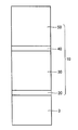
도 1은 본 발명의 실시예에서의 표면 피복 질화붕소 소결체 공구의 구성의 일례를 나타내는 단면도.
도 2는 본 발명의 실시예에서의 표면 피복 질화붕소 소결체 공구의 주요부의 구성의 일례를 나타내는 단면도. BRIEF DESCRIPTION OF THE DRAWINGS Fig. 1 is a cross-sectional view showing an example of the configuration of a surface-coated boron nitride sintered tool in an embodiment of the present invention. Fig.
2 is a cross-sectional view showing an example of the configuration of main parts of a surface-coated boron nitride sintered tool in an embodiment of the present invention.
이하, 본 발명에 관해 더욱 상세히 설명한다. 또, 이하의 실시형태의 설명에서는 도면을 이용하여 설명하고 있지만, 본원의 도면에 있어서 동일한 참조 부호를 붙인 것은, 동일 부분 또는 상당 부분을 나타내고 있다. Hereinafter, the present invention will be described in more detail. In the following description of the embodiments, description is made with reference to the drawings. In the drawings of the present application, the same reference numerals denote the same or substantially equivalent parts.
<표면 피복 질화붕소 소결체 공구의 구성> ≪ Construction of surface-coated boron nitride sintered tool >
본 발명에 따른 표면 피복 질화붕소 소결체 공구의 적어도 절삭날 부분은, 입방정 질화붕소 소결체(이하에서는 「cBN 소결체」로 기재한다. 「cBN」은 「cubic Boron Nitride」의 약어이다.)와, cBN 소결체의 표면 상에 형성된 피복층을 포함한다. 이와 같은 기본적 구성을 갖는 표면 피복 질화붕소 소결체 공구는, 소결 합금이나 난삭 주철의 기계 가공(예를 들면 절삭 가공) 또는 소입강의 가공에 있어서 특히 유효하게 이용할 수 있는 것 외에, 이들 이외의 일반적인 금속의 각종 가공에 있어서도 바람직하게 이용할 수 있다. At least a cutting edge portion of the surface-coated boron nitride sintered tool according to the present invention is formed by a cubic boron nitride sintered body (hereinafter referred to as "cBN sintered body", "cBN" is an abbreviation of "cubic boron nitride" And a coating layer formed on the surface of the substrate. The surface-coated boron nitride sintered tool having such a basic structure can be used particularly effectively in the machining (for example, cutting) of a sintered alloy or a difficult cast iron or in the processing of a quench steel, And can be suitably used for various kinds of processing.
<cBN 소결체> <cBN sintered body>
cBN 소결체는, 표면 피복 질화붕소 소결체 공구의 절삭날 부분 중 그 공구의 기재를 구성하는 것이며, 30 체적% 이상 80 체적% 이하의 입방정 질화붕소(이하에서는 「cBN」으로 기재함)를 포함하고, 결합상을 더 포함한다. 여기서, 결합상은, 원소의 주기율표의 제4족 원소, 제5족 원소 및 제6족 원소의 질화물, 탄화물, 붕화물, 산화물 및 이들의 고용체를 포함하는 군 중에서 선택된 적어도 1종의 화합물과 알루미늄 화합물과 불가피 불순물을 포함하고, cBN끼리를 서로 결합한다. cBN 소결체가 30 체적% 이상의 cBN을 포함하고 있으면, 표면 피복 질화붕소 소결체 공구의 기재의 내마모성의 저하를 방지할 수 있다. 또한, cBN 소결체가 80 체적% 이하의 cBN을 포함하고 있으면, cBN 소결체에 있어서 cBN을 분산시킬 수 있기 때문에, 결합상에 의한 cBN끼리의 접합 강도를 확보할 수 있다. 본 명세서에서는, cBN의 함유 체적율은 다음에 나타내는 방법에 따라서 구해진 것이다. cBN 소결체를 경면 연마하고, 임의의 영역의 cBN 소결체 조직의 반사 전자 이미지를 전자 현미경으로 2000배로 사진 촬영한다. 이때, cBN으로 이루어진 입자(이하에서는 「cBN 입자」로 기재한다.)는 흑색 영역이 되고, 결합상은 회색 영역 또는 백색 영역이 된다. 촬영된 cBN 소결체 조직의 사진으로부터 cBN 소결체 영역과 결합상 영역을 화상 처리에 의해 2치화(値化)하여, cBN 입자의 점유 면적을 구한다. 구해진 cBN 입자의 점유 면적을 이하에 나타내는 식에 대입하면, cBN의 함유 체적율이 구해진다.The cBN sintered body constitutes the base of the tool in the cutting edge portion of the surface-coated boron nitride sintered tool, and contains cubic boron nitride (hereinafter referred to as " cBN ") of 30 volume% or more and 80 volume% or less, Lt; / RTI > Here, the bonded phase includes at least one compound selected from the group consisting of nitrides, carbides, borides, oxides and solid solutions of Group 4 elements, Group 5 elements and Group 6 elements of the periodic table of the elements, And inevitable impurities, and combine the cBNs with each other. When the cBN sintered body contains cBN of 30 vol% or more, it is possible to prevent the wear resistance of the substrate of the surface-coated boron nitride sintered tool from deteriorating. If the cBN sintered body contains cBN of 80 vol% or less, the cBN can be dispersed in the cBN sintered body, so that the bonding strength of the cBNs due to the bonded phase can be ensured. In the present specification, the volume fraction of cBN is obtained by the following method. The cBN sintered body is mirror-polished, and the reflection electron image of the cBN sintered body structure in an arbitrary region is photographed at 2000 times with an electron microscope. At this time, the particles made of cBN (hereinafter referred to as " cBN particles ") become black regions, and the bound phases become gray regions or white regions. From the photographed cBN sintered body texture, the cBN sintered body region and the bonded phase region are binarized (processed) by image processing to obtain the occupied area of cBN particles. Substituting the obtained occupied area of the cBN grains into the equation shown below, the volume fraction of cBN is obtained.
(cBN의 함유 체적율)=(cBN 입자의 점유 면적)÷(촬영된 cBN 소결체 조직의 면적)×100. (volume fraction of cBN) = (occupied area of cBN particles) / (area of captured cBN sintered body structure) x 100.
바람직하게는, cBN 소결체가 50 체적% 이상 65 체적% 이하의 cBN을 포함하는 것이다. cBN 소결체가 50 체적% 이상의 cBN을 포함하고 있으면, 내마모성과 내결손성의 밸런스가 우수한 표면 피복 질화붕소 소결체 공구의 기재를 제공할 수 있다. 또한, cBN 소결체가 65 체적% 이하의 cBN을 포함하고 있으면, 결합상에 의한 cBN끼리의 접합 강도를 높일 수 있다. Preferably, the cBN sintered body contains 50% by volume or more and 65% by volume or less of cBN. When the cBN sintered body contains 50 vol% or more of cBN, it is possible to provide a substrate of a surface-coated boron nitride sintered tool having excellent balance between abrasion resistance and pitting resistance. When the cBN sintered body contains cBN of 65% by volume or less, the bonding strength of the cBNs due to the bonded phase can be increased.
바람직하게는, cBN 소결체와 피복층의 계면에서는, cBN 입자가 결합상보다 피복층측으로 돌출되어 있는 것이다. 이에 따라, cBN 소결체와 피복층의 밀착성을 높일 수 있다. 보다 바람직하게는, cBN 입자와 결합상의 단차가 0.05 ㎛ 이상 1.0 ㎛ 이하인 것이다. 이 단차가 0.05 ㎛ 이상이면, 앵커 효과를 얻을 수 있다. 또한, 이 단차가 1.0 ㎛ 이하이면, cBN 입자가 cBN 소결체로부터 탈락하는 것을 방지할 수 있다. 더욱 바람직하게는, cBN 입자와 결합상의 단차가 0.1 ㎛ 이상 0.5 ㎛ 이하인 것이다. 이 단차가 0.1 ㎛ 이상이면, 앵커 효과를 유효하게 얻을 수 있다. 또한, 이 단차가 0.5 ㎛ 이하이면, cBN 입자가 cBN 소결체로부터 탈락하는 것을 더욱 방지할 수 있다. 본 명세서에서는, 상기 단차는, 후술하는 피복층의 전체 두께 등의 측정 방법과 동일한 방법에 따라서 측정된 것이다. Preferably, in the interface between the cBN sintered body and the coating layer, the cBN particles are projected toward the coating layer rather than the bonded phase. As a result, the adhesion between the cBN sintered body and the coating layer can be enhanced. More preferably, the step difference between the cBN grains and the binding phase is not less than 0.05 mu m and not more than 1.0 mu m. If the step is 0.05 占 퐉 or more, an anchor effect can be obtained. If the step is 1.0 占 퐉 or less, it is possible to prevent the cBN particles from falling off from the cBN sintered body. More preferably, the step difference of the cBN grains and the binding phase is 0.1 mu m or more and 0.5 mu m or less. If the step is 0.1 mu m or more, the anchor effect can be effectively obtained. Further, when the step is 0.5 탆 or less, it is possible to further prevent the cBN particles from falling off from the cBN sintered body. In the present specification, the step is measured according to the same method as the method of measuring the total thickness of the coating layer, which will be described later.
바람직하게는, cBN 소결체에서의 cBN의 체적 함유율은, cBN 소결체와 피복층의 계면으로부터 cBN 소결체의 내부로 갈수록 높아지는 것이다. 이에 따라, cBN 소결체와 피복층의 계면에서는, 결합상의 체적 함유율이 cBN의 체적 함유율보다 높기 때문에, cBN 소결체와 피복층의 밀착성을 높일 수 있다. 한편, cBN 소결체의 내부에서는, cBN의 체적 함유율이 결합상의 체적 함유율보다 높기 때문에, cBN 소결체의 내결손성을 향상시킬 수 있다. 예를 들면, cBN의 체적 함유율은, 피복층과의 계면측(cBN 소결체와 피복층의 계면으로부터 cBN 소결체의 내부를 향하여 0 ㎛ 이상 20 ㎛ 이하 떨어진 영역)에서는 40 체적%이고, cBN 소결체의 두께 방향 중앙 부근(cBN 소결체와 피복층의 계면으로부터 cBN 소결체의 내부를 향하여 20 ㎛ 초과 100 ㎛ 이하 떨어진 영역)에서는 60 체적%이다. Preferably, the volume content of cBN in the sintered body of cBN increases from the interface between the sintered body of cBN and the coating layer to the inside of the sintered body of cBN. Thus, at the interface between the cBN sintered body and the coating layer, the volume content of the bonded phase is higher than the volume content of cBN, so that the adhesion between the cBN sintered body and the coating layer can be enhanced. On the other hand, in the inside of the cBN sintered body, since the volume content of cBN is higher than the volume content of the bonded phase, the resistance of the cBN sintered body can be improved. For example, the volume content of cBN is 40% by volume at the interface side with respect to the coating layer (a region of 0 占 퐉 or more and 20 占 퐉 or less from the interface between the cBN sintered body and the coating layer toward the inside of the cBN sintered body) (60% by volume in the region where the distance from the interface between the cBN sintered body and the coating layer to the inside of the cBN sintered body is more than 20 占 퐉 and not more than 100 占 퐉).
바람직하게는, cBN 소결체에 포함되는 cBN 입자의 입경은, cBN 소결체와 피복층의 계면으로부터 cBN 소결체의 내부로 갈수록 커지는 것이다. 이에 따라, cBN 소결체와 피복층의 계면에서는, cBN 입자의 입경은 작기 때문에, cBN 소결체와 피복층의 밀착성을 높일 수 있다. 한편, cBN 소결체의 내부에서는, cBN 입자의 입경은 크기 때문에 인성을 높일 수 있다. 예를 들면, cBN 입자의 입경은, cBN 소결체와 피복층의 계면으로부터 cBN 소결체의 내부를 향하여 0 ㎛ 이상 20 ㎛ 이하 떨어진 영역에서는 0.1 ㎛ 이상 1 ㎛ 이하이고, cBN 소결체와 피복층의 계면으로부터 cBN 소결체의 내부를 향하여 20 ㎛ 초과 300 ㎛ 이하 떨어진 영역에서는 2 ㎛ 이상 10 ㎛ 이하이다. 본 명세서에서는, cBN 입자의 입경은 다음에 나타내는 방법에 따라서 구해진 것이다. cBN의 함유 체적율을 구할 때에 얻어진 cBN 소결체 조직의 반사 전자 이미지에 있어서 cBN 입자에 외접하는 원의 직경을 측정하고, 측정된 직경을 cBN 입자의 입경으로 하고 있다. Preferably, the particle diameter of the cBN particles contained in the cBN sintered body increases from the interface between the cBN sintered body and the coating layer toward the inside of the cBN sintered body. Accordingly, since the particle diameter of the cBN particles is small at the interface between the cBN sintered body and the coating layer, the adhesion between the cBN sintered body and the coating layer can be enhanced. On the other hand, in the interior of the cBN sintered body, since the particle diameter of the cBN particles is large, the toughness can be increased. For example, the particle diameter of the cBN particles is not less than 0.1 탆 and not more than 1 탆 in a range of 0 탆 to 20 탆 apart from the interface between the cBN sintered body and the coating layer toward the inside of the cBN sintered body, And not less than 2 占 퐉 and not more than 10 占 퐉 in a region where the distance is not more than 20 占 퐉 and not more than 300 占 퐉 toward the inside. In this specification, the particle diameter of the cBN particles is obtained by the following method. The diameter of the circle circumscribing the cBN grains in the reflection electron image of the cBN sintered body structure obtained when the contained volume ratio of cBN is obtained is measured and the measured diameter is defined as the grain diameter of the cBN grains.
또, cBN 소결체는, 표면 피복 질화붕소 소결체 공구의 절삭날 부분에 설치되어 있으면 된다. 그 때문에, 표면 피복 질화붕소 소결체 공구의 기재는, cBN 소결체로 이루어진 절삭날 부분과, cBN 소결체와는 상이한 재료(예를 들면 초경합금)로 이루어진 기재 본체를 포함하고 있어도 좋다. 이 경우, cBN 소결체로 이루어진 절삭날 부분은 납재 등을 통해 기재 본체에 접착되어 있는 것이 바람직하고, 납재의 재료로는, 접합 강도 또는 융점을 고려하여 선정할 수 있다. 또한, cBN 소결체는, 표면 피복 질화붕소 소결체 공구의 기재 전체를 구성하고 있어도 좋다. The cBN sintered body may be provided at the cutting edge portion of the surface-coated boron nitride sintered tool. Therefore, the substrate of the surface-coated boron nitride sintered tool may include a cutting edge portion made of a cBN sintered body and a base body made of a material different from that of the cBN sintered body (for example, cemented carbide). In this case, it is preferable that the cutting edge portion made of the cBN sintered body is bonded to the base body through a brazing material or the like, and the brazing material can be selected in consideration of the bonding strength or the melting point. The cBN sintered body may constitute the entire substrate of the surface-coated boron nitride sintered tool.
<피복층> ≪ Coated layer &
피복층은 A층과 B층을 포함한다. 본 발명의 피복층은 A층과 B층을 포함하는 한, A층 및 B층 이외에 다른 층을 포함하고 있어도 지장이 없다. 이와 같은 다른 층으로는, 예를 들면 후술하는 바와 같은 A층과 B층 사이에 형성되는 C층 또는 최하층인 D층 등을 들 수 있지만, 이들에만 한정되는 것은 아니다. The covering layer includes an A layer and a B layer. The coating layer of the present invention may contain other layers other than the A layer and the B layer as long as it includes the A layer and the B layer. Such another layer may be, for example, a C layer formed between the A layer and the B layer as described below, or a D layer being the lowermost layer, but the present invention is not limited thereto.
피복층의 두께는 0.26 ㎛ 이상 15 ㎛ 이하이다. 피복층의 두께가 0.26 ㎛ 이상이면, 피복층의 두께가 얇은 것에 기인하는 표면 피복 질화붕소 소결체 공구의 내마모성의 저하를 방지할 수 있다. 피복층의 두께가 15 ㎛ 이하이면, 절삭 초기의 피복층의 내(耐)칩핑성을 높일 수 있다. 바람직하게는, 피복층의 두께가 1.0 ㎛ 이상 4.0 ㎛ 이하이다. The thickness of the coating layer is 0.26 탆 or more and 15 탆 or less. When the thickness of the coating layer is 0.26 m or more, deterioration of wear resistance of the surface-coated boron nitride sintered tool caused by a thin coating layer can be prevented. When the thickness of the coating layer is 15 m or less, the resistance to chipping of the coating layer at the beginning of cutting can be enhanced. Preferably, the thickness of the coating layer is 1.0 占 퐉 or more and 4.0 占 퐉 or less.
본 명세서에서는, 피복층의 전체 두께 및 후술하는 각 층의 두께 및 적층수는 모두, 표면 피복 질화붕소 소결체 공구를 절단하고, 그 단면을 SEM(주사형 전자 현미경) 또는 TEM(투과형 전자 현미경)을 이용하여 관찰함으로써 구해진 것이다. 또한, 피복층을 구성하는 후술하는 바와 같은 각 층의 조성은, SEM 또는 TEM이 부대된 EDX 분석기(에너지 분산형 X선 분석기)를 이용하여 측정된 것이다. In the present specification, the total thickness of the coating layer, the thickness of each layer to be described later, and the number of layers are all determined by cutting the surface-coated boron nitride sintered tool and measuring its cross section using an SEM (scanning electron microscope) or a TEM (transmission electron microscope) . The composition of each layer as described below constituting the coating layer was measured using an EDX analyzer (energy dispersive X-ray analyzer) accompanied by SEM or TEM.
피복층은, 표면 피복 질화붕소 소결체 공구의 절삭날 부분에만 형성되어 있으면 되지만, 표면 피복 질화붕소 소결체 공구의 기재의 표면 전면을 피복하고 있어도 좋고, 절삭날 부분과는 상이한 부분의 일부에 있어서 형성되어 있지 않아도 좋다. 또한, 절삭날 부분과는 상이한 부분에서는, 피복층의 일부의 적층 구성이 부분적으로 상이해도 좋다. The coating layer may be formed only on the cutting edge portion of the surface-coated boron nitride sintered tool, but it may be formed so as to cover the entire surface of the base material of the surface-coated boron nitride sintered tool and be formed in a part of the portion different from the cutting edge portion You do not need to. In a portion different from the cutting edge portion, the lamination structure of a part of the coating layer may be partially different.
<A층> <Floor A>
A층은, MLaza1(M은 원소의 주기율표의 제4족 원소, 제5족 원소 및 제6족 원소, Al 및 Si 중 1종 이상을 나타내고, La는 B, C, N 및 O 중 1종 이상을 나타내고, za1은 0.85 이상 1.0 이하이다)로 이루어진다. 이에 따라, A층은 매끄럽게 마모된다. 다르게 표현하면, A층은, 박리, 크랙 또는 칩핑 등을 수반하지 않고 마모된다. 따라서, 표면 피복 질화붕소 소결체 공구의 내크레이터 마모성 또는 내여유면 마모성 등을 높일 수 있다. The layer A is composed of one or more of B, C, N, and O, wherein MLa za1 (M represents at least one of Group 4 element, Group 5 element and Group 6 element in the periodic table of elements, Al and Si, And za1 is 0.85 or more and 1.0 or less). As a result, the A layer is worn smoothly. In other words, the A layer is worn without peeling, cracking, or chipping. Therefore, it is possible to increase the crater wear resistance or the margin surface wear resistance of the surface-coated boron nitride sintered tool.
바람직하게는, A층은, (Ti1 - xaMaxa)(C1- za2Nza2)(Ma는 Ti를 제외한 원소의 주기율표의 제4족 원소, 제5족 원소 및 제6족 원소, Al 및 Si 중 1종 이상을 나타내고, xa는 0 이상 0.7 이하이고, za2는 0 이상 1 이하이다)로 이루어진 것이다. A층이 Ti를 포함하고 있으면, 마모시의 A층의 박리, 크랙 또는 칩핑 등을 더욱 방지할 수 있다. 보다 바람직하게는, Ma의 조성 xa가 0 이상 0.3 이하인 것이다. 이에 따라, 마모시의 A층의 박리, 크랙 또는 칩핑 등을 더욱 방지할 수 있다. 또, A층이 (Ti1 -xa(1)-xa(2)Ma(1)xa(1)Ma(2)xa(2))(C1-za2Nza2)로 이루어진 경우에는, xa(1)과 xa(2)의 합이 상기 범위를 만족시키는 것이 바람직하다. 이것은, 이하에 나타내는 B층, C층 및 D층에 있어서도 말할 수 있다. Preferably, the layer A is at least one element selected from the group consisting of ( Ti1 - xa Ma xa ) (C 1- za2 N za2 ) (Ma is a Group 4 element, a Group 5 element and a Group 6 element in the periodic table of elements except Ti, And Si, xa is not less than 0 and not more than 0.7, and za2 is not less than 0 and not more than 1). When the layer A contains Ti, peeling, cracking or chipping of the layer A at the time of abrasion can be further prevented. More preferably, the composition xa of Ma is 0 or more and 0.3 or less. Thus, it is possible to further prevent peeling, cracking, chipping, and the like of the A layer at the time of abrasion. When the layer A is composed of (Ti 1 -xa (1) -xa (2) Ma (1) xa (1) Ma (2) xa (2) ) (C 1 -za 2 Nza2 ) 1) and xa (2) satisfy the above range. This is also true for the B, C and D layers shown below.
바람직하게는, A층에서는, N의 조성은, cBN 소결체측으로부터 그 A층의 표면측으로 갈수록 스텝형 또는 경사형으로 변화하는 것이다. 예를 들면 A층의 cBN 소결체측에 있어서 N의 조성이 크면, 내결손성 및 내박리성을 높일 수 있다. 또한, A층의 표면측에 있어서 N의 조성이 작으면, 마모시의 A층의 박리, 크랙 또는 칩핑 등을 더욱 방지할 수 있다. 여기서, 「N의 조성이 cBN 소결체측으로부터 A층의 표면측으로 갈수록 스텝형으로 변화한다」란, N의 조성이 cBN 소결체측으로부터 A층의 표면측으로 갈수록 불연속적으로 감소 또는 증가하는 것을 의미하며, 예를 들면 N의 조성이 서로 다른 2 이상의 층을 적층함으로써 얻어지는 구성이다. 또한, 「N의 조성이 cBN 소결체측으로부터 A층의 표면측으로 갈수록 경사형으로 변화한다」란, N의 조성이 cBN 소결체측으로부터 A층의 표면측으로 갈수록 연속적으로 감소 또는 증가하는 것을 의미하며, 예를 들면 N의 원료 가스와 C의 원료 가스의 유량비를 연속적으로 변화시켜 형성함으로써 얻어지는 구성이다. Preferably, in the layer A, the composition of N changes stepwise or inclined from the cBN sintered body side toward the surface side of the layer A, For example, if the composition of N is large on the cBN sintered body side of the A layer, the resistance to cracking and the peel resistance can be enhanced. When the composition of N on the surface side of the layer A is small, it is possible to further prevent peeling, cracking, chipping, and the like of the layer A at the time of abrasion. Here, "the composition of N changes stepwise from the cBN sintered body side toward the surface side of the A layer" means that the composition of N decreases or increases discontinuously from the cBN sintered body side toward the surface side of the A layer, For example, by laminating two or more layers having different N compositions. Means that the composition of N is continuously decreased or increased from the cBN sintered body side toward the surface side of the A layer, The flow rate ratio of the source gas of N and the source gas of C is continuously changed.
바람직하게는, A층은, 그 A층의 표면측에, cBN 소결체측보다 C의 조성이 높은 영역을 갖는 것이다. 이것에 의해서도, A층의 cBN 소결체측에서는 내결손성 및 내박리성을 높일 수 있고, A층의 표면측에서는 마모시의 A층의 박리, 크랙 또는 칩핑 등을 더욱 방지할 수 있다. 여기서, A층의 cBN 소결체측이란, cBN 소결체에 가장 가까이에 위치하는 A층의 면으로부터 A층의 내부를 향하여 0 ㎛ 이상 A층의 두께의 1/2배 이하 떨어진 영역, 및, cBN 소결체에 가장 가까이에 위치하는 A층의 면으로부터 A층의 내부를 향하여 0 ㎛ 이상 0.1 ㎛ 이하 떨어진 영역 중 좁은 쪽을 의미한다. 또한, A층의 표면측이란, A층의 cBN 소결체측과는 반대측을 의미하고, A층의 cBN 소결체측과는 상이한 부분을 의미한다. Preferably, the A layer has a region having a higher composition of C than the cBN sintered body side on the surface side of the A layer. This also makes it possible to increase the resistance to cracking and peel resistance on the side of the cBN sintered body of the A layer, and further to prevent peeling, cracking or chipping of the A layer at the time of abrasion on the surface side of the A layer. Here, the side of the cBN sintered body of the A layer means a region which is 0 占 퐉 or more and 1/2 times or less the thickness of the A layer from the side of the A layer located nearest to the sintered body of cBN toward the inside of the A layer, Means a region narrower than 0 占 퐉 or more and 0.1 占 퐉 or less from the face of the closest A layer toward the inside of the A layer. The surface side of the A layer means a side opposite to the cBN sintered body side of the A layer and means a portion different from the cBN sintered body side of the A layer.
A층의 두께는 0.2 ㎛ 이상 10 ㎛ 이하이다. A층의 두께가 0.2 ㎛ 이상이면, 내크레이터 마모성 또는 내여유면 마모성 등이 우수한 표면 피복 질화붕소 소결체 공구를 제공할 수 있다. 한편, A층의 두께가 10 ㎛를 초과하면, 표면 피복 질화붕소 소결체 공구의 내크레이터 마모성 또는 내여유면 마모성 등을 더욱 향상시키는 것이 어려운 경우가 있다. The thickness of the A layer is 0.2 占 퐉 or more and 10 占 퐉 or less. When the thickness of the A layer is 0.2 탆 or more, it is possible to provide a surface-coated boron nitride sintered tool having excellent crater wear resistance or margin surface wear resistance. On the other hand, when the thickness of the A layer exceeds 10 mu m, it may be difficult to further improve the crater wear resistance or the margin surface wear resistance of the surface-coated boron nitride sintered tool.
바람직하게는, A층이 B층보다 표면 피복 질화붕소 소결체 공구의 표면측에 형성되어 있는 것이다. 이에 따라, A층이 매끄럽게 마모되어 크랙의 발생을 방지할 수 있다. 또한, 크랙이 발생한 경우라 하더라도, B층이, 발생한 크랙의 기재측으로 전파하는 것을 방지할 수 있다. Preferably, the layer A is formed on the surface side of the surface-coated boron nitride sintered tool than the layer B is. As a result, the A layer is smoothly worn and cracks can be prevented from occurring. Further, even when cracks are generated, it is possible to prevent the B layer from propagating to the substrate side of the generated cracks.
<B층> <Floor B>
B층은, 조성이 상이한 2종 이상의 박막층이 교대로 각각 하나 이상 적층되어 이루어진다. 이하에서는, B층으로서, B1 박막층과 B2 박막층이 교대로 각각 하나 이상 적층되어 구성된 것을 들지만, 본 발명의 B층은, B1 박막층과 B2 박막층을 포함하는 한, B1 박막층 및 B2 박막층 이외에 다른 층을 포함하고 있어도 지장이 없다. B층의 두께는 0.06 ㎛ 이상 5 ㎛ 이하이다. The B layer is formed by laminating at least two or more thin film layers of different compositions alternately. Hereinafter, the B1 layer and the B2 thin film layer are alternately stacked as the B layer. However, the B layer of the present invention may contain other layers other than the B1 thin film layer and the B2 thin film layer as long as the B1 thin film layer and the B2 thin film layer are included. There is no problem even if it includes. The thickness of the B layer is 0.06 탆 or more and 5 탆 or less.
바람직하게는, B층 전체에서의 Si 조성의 평균치가 0.003 이상 0.1 이하인 것이다. 이에 따라, B층의 내박리성을 높일 수 있기 때문에, 산소가 B층과 A층 또는 기재와의 계면에 침입하는 것을 방지할 수 있다. B층 전체에서의 Si 조성의 평균치는, 보다 바람직하게는 0.005 이상 0.07 이하이고, 더욱 바람직하게는 0.007 이상 0.05 이하이다. 본 명세서에서는, B층 전체에서의 Si 조성의 평균치는, 다음 계산식을 이용하여 구해진 것이다. Preferably, the average value of the Si composition in the entire B layer is 0.003 or more and 0.1 or less. As a result, the peeling resistance of the B layer can be enhanced, so that oxygen can be prevented from entering the interface between the B layer and the A layer or the substrate. The average value of the Si composition in the entire layer B is more preferably from 0.005 to 0.07, and still more preferably from 0.007 to 0.05. In this specification, the average value of the Si composition in the entire B layer is obtained by using the following calculation formula.
(B층 전체에서의 Si 조성의 평균치)=[{(B층을 구성하는 각 층의 Si 조성)×(그 각 층의 두께)}의 총합]÷(B층 전체의 두께). (The sum of the Si composition of the entire B layer) = {(the Si composition of each layer constituting the B layer) x (the thickness of each layer)} / (the thickness of the entire B layer).
B1 박막층은, 조성이 상이한 2종 이상의 화합물층이 교대로 각각 하나 이상 적층되어 이루어진다. 이하에서는, B1 박막층으로서, B1a 화합물층과 B1b 화합물층이 교대로 각각 하나 이상 적층되어 구성된 것을 들지만, 본 발명의 B1 박막층은, B1a 화합물층과 B1b 화합물층을 포함하는 한, B1a 화합물층 및 B1b 화합물층 이외에 다른 층을 포함하고 있어도 지장이 없다. B1 박막층의 두께는 30 nm보다 크고 200 nm 미만이다. The B1 thin film layer is formed by laminating two or more kinds of compound layers having different compositions alternately. The B1 thin film layer of the present invention may contain other layers besides the B1a compound layer and the B1b compound layer as long as the B1 thin film layer contains the B1a compound layer and the B1b compound layer as long as the B1 thin film layer is constituted by alternately stacking one or more B1a compound layers and B1b compound layers. There is no problem even if it includes. The thickness of the B1 thin film layer is greater than 30 nm and less than 200 nm.
B1a 화합물층은, (Ti1 - xb1 - yb1Sixb1M1yb1)(C1- zb1Nzb1)(M1은 Ti를 제외한 원소의 주기율표의 제4족 원소, 제5족 원소 및 제6족 원소 및 Al 중 1종 이상을 나타내고, xb1은 0.01 이상 0.25 이하이고, yb1은 0 이상 0.7 이하이고, zb1은 0.4 이상 1 이하이다)로 이루어진다. B1a 화합물층의 두께는 0.5 nm 이상 30 nm 미만이다. B1a compound layer, (Ti 1 - xb1 - yb1 Si xb1 M1 yb1) (C 1- zb1 N zb1) (M1 is the periodic table of the elements of the fourth group elements except Ti, a Group 5 element and a group 6 element and Al Xb1 is not less than 0.01 and not more than 0.25, yb1 is not less than 0 and not more than 0.7, and zb1 is not less than 0.4 and not more than 1). The thickness of the B1a compound layer is 0.5 nm or more and less than 30 nm.
B1b 화합물층은, (Al1 - xb2M2xb2)(C1- zb2Nzb2)(M2는 원소의 주기율표의 제4족 원소, 제5족 원소 및 제6족 원소 및 Si 중 1종 이상을 나타내고, xb2는 0.2 이상 0.77 이하이고, zb2는 0.4 이상 1 이하이다)로 이루어진다. M2는, Ti 및 Cr 중 적어도 하나를 나타내는 것이 바람직하다. M2의 조성 xb2는, 바람직하게는 0.25 이상 0.5 이하이고, 보다 바람직하게는 0.25 이상 0.4 이하이다. B1b 화합물층의 두께는 0.5 nm 이상 30 nm 미만이다. B1b compound layer, (Al 1 - xb2 M2 xb2 ) (C 1- zb2 N zb2) (M2 represents a periodic table Group 4 element, a Group 5 element and a group 6 element, and at least one of the elements Si, xb2 is not less than 0.2 and not more than 0.77, and zb2 is not less than 0.4 and not more than 1). M2 preferably represents at least one of Ti and Cr. The composition xb2 of M2 is preferably 0.25 or more and 0.5 or less, and more preferably 0.25 or more and 0.4 or less. The thickness of the B1b compound layer is 0.5 nm or more and less than 30 nm.
B2 박막층은, (Al1 - xb3M3xb3)(C1- zb3Nzb3)(M3은 원소의 주기율표의 제4족 원소, 제5족 원소 및 제6족 원소 및 Si 중 1종 이상을 나타내고, xb3은 0.2 이상 0.77 이하이고, zb3은 0.4 이상 1 이하이다)로 이루어진다. M3은, 바람직하게는 Ti 및 Cr 중 적어도 하나를 나타내고, 보다 바람직하게는 M2와 동일한 원소를 나타낸다. M3의 조성 xb3은, 바람직하게는 0.25 이상 0.5 이하이고, 보다 바람직하게는 0.25 이상 0.4 이하이고, 더욱 바람직하게는 M2의 조성 xb2와 동일한 값이다. B2 박막층의 두께는 30 nm보다 크고 200 nm 미만이다. The B2 thin film layer is formed of (Al 1 - xb 3 M 3 xb 3 ) (C 1 zb 3 N zb 3 ) (M3 represents at least one of Group 4 element, Group 5 element and Group 6 element and Si in the periodic table of the elements, xb3 is not less than 0.2 and not more than 0.77, and zb3 is not less than 0.4 and not more than 1). M3 preferably represents at least one of Ti and Cr, and more preferably represents the same element as M2. The composition xb3 of M3 is preferably 0.25 or more and 0.5 or less, more preferably 0.25 or more and 0.4 or less, and still more preferably the same value as the composition xb2 of M2. The thickness of the B2 thin film layer is greater than 30 nm and less than 200 nm.
바람직하게는, B1 박막층의 평균 두께 t1과 B2 박막층의 평균 두께 t2의 비인 t2/t1이 0.5<t2/t1≤10.0을 만족시키는 것이다. 이에 따라, 표면 피복 질화붕소 소결체 공구의 내경계 마모성 등(예를 들면, 설비 강성 또는 워크 강성 등이 낮은 환경하에서 소입강의 가공 등을 행한 경우에 표면 피복 질화붕소 소결체 공구의 내경계 마모성 등)을 보다 향상시킬 수 있다. 본 명세서에서는, B1 박막층의 평균 두께 t1은, 다음 계산식을 이용하여 구해진 것이다. B2 박막층의 평균 두께 t2도 동일하다.Preferably, t2 / t1, which is the ratio of the average thickness t1 of the B1 thin film layer to the average thickness t2 of the B2 thin film layer, satisfies 0.5 < t2 / t1 &le; As a result, the wear resistance and the like of the surface-coated boron nitride sintered tool (for example, the wear resistance of the inner surface of the surface-coated boron nitride sintered tool when the workpiece is machined or the like under an environment with low rigidity or work stiffness) Can be improved. In this specification, the average thickness t1 of the B1 thin film layer is obtained by using the following calculation formula. The average thickness t2 of the B2 thin film layer is also the same.
(B1 박막층의 평균 두께 t1)=(B1 박막층의 두께의 합계)÷(B1 박막층의 층수). (Average thickness t1 of B1 thin film layer) = (total thickness of B1 thin film layer) / (number of layers of B1 thin film layer).
보다 바람직하게는, t2/t1이 0.7<t2/t1≤5.0을 만족시키는 것이다. 이에 따라, 표면 피복 질화붕소 소결체 공구의 내경계 마모성 등(예를 들면, 설비 강성 또는 워크 강성 등이 낮은 환경하에서 소입강의 가공 등을 행한 경우에 표면 피복 질화붕소 소결체 공구의 내경계 마모성 등)을 보다 향상시킬 수 있다. 따라서, 반복되는 충격 또는 진동 등에 대하여 우수한 내마모성을 갖는 표면 피복 질화붕소 소결체 공구를 제공할 수 있다. 더욱 바람직하게는, t2/t1이 1.1<t2/t1≤4.5를 만족시키는 것이다. More preferably, t2 / t1 satisfies 0.7 < t2 / t1 &le; 5.0. As a result, the wear resistance and the like of the surface-coated boron nitride sintered tool (for example, the wear resistance of the inner surface of the surface-coated boron nitride sintered tool when the workpiece is machined or the like under an environment with low rigidity or work stiffness) Can be improved. Therefore, it is possible to provide a surface-coated boron nitride sintered tool having excellent abrasion resistance against repeated impacts or vibrations. More preferably, t2 / t1 satisfies 1.1 < t2 / t1 &le; 4.5.
더욱 바람직하게는, A층이 B층보다 표면측에 형성되어 있는 경우에는, t2/t1은, cBN 소결체측에서는 1.1<t2/t1≤5.0을 만족시키고, A층측으로 갈수록 작아지고, A층측에서는 0.7<t2/t1<2를 만족시키는 것이다. 이에 따라, B층의 A층측에서는, 크랙의 발생을 방지할 수 있고, B층의 cBN 소결체측에서는, 크랙이 cBN 소결체측으로 전파하는 것을 방지할 수 있다. 여기서, B층의 A층측이란, A층에 가장 가까이에 위치하는 B1 박막층 및 B2 박막층을 의미한다. 또한, B층의 cBN 소결체측이란, cBN 소결체에 가장 가까이에 위치하는 B1 박막층 및 B2 박막층을 의미한다. More preferably, when A layer is formed on the surface side of the B layer, t2 / t1 satisfies 1.1 < t2 / t1 &le; 5.0 on the side of the cBN sintered body and becomes smaller toward the A layer side, < t2 / t1 < 2. Thus, cracks can be prevented from occurring on the A-layer side of the B-layer, and cracks can be prevented from propagating to the cBN sintered body side on the cBN sintered body side of the B-layer. Here, the A layer side of the B layer means the B1 thin film layer and the B2 thin film layer located closest to the A layer. The cBN sintered body side of the B layer means the B1 thin film layer and the B2 thin film layer located closest to the cBN sintered body.
<C층> <C layer>
바람직하게는, 피복층이 A층과 B층 사이에 형성된 C층을 더 포함하는 것이며, C층이 McLczc(Mc는 원소의 주기율표의 제4족 원소, 제5족 원소 및 제6족 원소, Al 및 Si 중 1종 이상을 나타내고, Lc는 B, C, N 및 O 중 1종 이상을 나타내고, zc는 0 이상 0.85 이하이다)로 이루어진 것이다. 이에 따라, A층과 B층의 밀착성을 높일 수 있다. 또한, A층이 B층보다 표면측에 형성되어 있는 경우에는, A층에서 발생한 크랙이 기재측으로 전파하는 것을 C층에서 정지시킬 수 있다. Preferably, the coating layer further comprises a C layer formed between the A layer and the B layer, wherein the C layer is composed of McLc zc (Mc is a Group 4 element, a Group 5 element and a Group 6 element of the periodic table of the elements, Al And Si, Lc represents at least one of B, C, N and O, and zc is at least 0 and at most 0.85. Thus, the adhesion between the A layer and the B layer can be enhanced. Further, when the layer A is formed on the surface side of the layer B, it is possible to stop the propagation of cracks generated in the layer A to the substrate side in the layer C.
보다 바람직하게는, C층의 두께가 0.005 ㎛ 이상 0.5 ㎛ 이하인 것이다. C층의 두께가 0.005 ㎛ 이상이면, C층을 형성함으로써 얻어지는 효과를 충분히 얻을 수 있다. C층의 두께가 0.5 ㎛ 이하이면, C층을 형성함으로써 피복층의 두께가 지나치게 커지는 것을 방지할 수 있다. 더욱 바람직하게는, C층의 두께가 0.01 ㎛ 이상 0.2 ㎛ 이하인 것이다. More preferably, the thickness of the C layer is 0.005 탆 or more and 0.5 탆 or less. When the thickness of the C layer is 0.005 m or more, the effect obtained by forming the C layer can be sufficiently obtained. When the thickness of the C layer is 0.5 占 퐉 or less, the thickness of the coating layer can be prevented from becoming excessively large by forming the C layer. More preferably, the thickness of the C layer is not less than 0.01 탆 and not more than 0.2 탆.
보다 바람직하게는, Lc의 조성 zc가 0보다 크고 0.7 미만인 것이다. Lc의 조성 zc가 0보다 크면, C층의 내열성 및 화학적인 내마모성을 높일 수 있기 때문에, A층에서 발생한 크랙이 기재측으로 전파하는 것을 C층에서 유효하게 정지시킬 수 있다. 더욱 바람직하게는, Lc의 조성 zc가 0.2 이상 0.5 이하인 것이다. More preferably, the composition zc of Lc is greater than 0 and less than 0.7. If the composition ratio zc of Lc is larger than 0, the heat resistance and the chemical abrasion resistance of the C layer can be increased, so that the propagation of the crack generated in the A layer to the substrate side can be effectively stopped in the C layer. More preferably, the composition zc of Lc is 0.2 or more and 0.5 or less.
보다 바람직하게는, C층은, A층 및 B층을 구성하는 원소 중 적어도 1 종 이상을 포함하는 것이다. C층이 A층을 구성하는 원소 중 적어도 1 종 이상을 포함하는 것이라면, A층과 C층의 밀착성을 높일 수 있다. C층이 B층을 구성하는 원소 중 적어도 1 종 이상을 포함하는 것이라면, B층과 C층의 밀착성을 높일 수 있다. 더욱 바람직하게는, C층은, A층 및 B층의 각각 중 C층측에 위치하는 부분을 구성하는 원소 중 적어도 1 종 이상을 포함하는 것이다. More preferably, the C layer includes at least one or more elements constituting the A layer and the B layer. If the C layer contains at least one or more elements constituting the A layer, the adhesion between the A layer and the C layer can be enhanced. If the C layer contains at least one or more elements constituting the B layer, the adhesion between the B layer and the C layer can be enhanced. More preferably, the C layer includes at least one or more elements constituting a portion located on the C layer side of each of the A layer and the B layer.
<D층> <D layer>
바람직하게는, 피복층이 기재와 B층 사이에 형성된 D층을 더 포함하는 것이며, D층이 MdLdzd(Md는 원소의 주기율표의 제4족 원소, 제5족 원소 및 제6족 원소, Al 및 Si 중 1종 이상을 나타내고, Ld는 B, C, N 및 O 중 1종 이상을 나타내고, zd는 0.85 이상 1.0 이하이다)로 이루어진 것이다. 이와 같은 D층은 cBN 소결체와의 밀착성이 우수하다. 따라서, 피복층이 D층을 더 포함하는 것이라면, cBN 소결체와 피복층의 밀착성을 높일 수 있다. 보다 바람직하게는, Ld가 N인 것이다. Preferably, the coating layer further comprises a D layer formed between the substrate and the B layer, wherein the D layer is MdLd zd wherein Md is a Group 4 element, a Group 5 element and a Group 6 element of the periodic table of the elements, Si, Ld represents at least one of B, C, N and O, and zd is at least 0.85 and at most 1.0). Such a D layer is excellent in adhesion to a sintered body of cBN. Therefore, if the coating layer further includes a D layer, the adhesion between the cBN sintered body and the coating layer can be enhanced. More preferably, Ld is N.
보다 바람직하게는, D층이 (Al1 - xdMd2xd)Ldzd(Md2는, 원소의 주기율표의 제4족 원소, 제5족 원소 및 제6족 원소 및 Si 중 1종 이상을 나타내고, xd는 0.25 이상 0.45 이하이다)로 이루어진 것이다. D층이 Al을 포함하고 있으면, cBN 소결체와 피복층의 밀착성을 보다 높일 수 있다. 더욱 바람직하게는, Md2가 Ti, Cr 및 V 중 적어도 1 종 이상인 것이다. More preferably, D layer is (Al 1 - xd Md2 xd) Ld zd (Md2 is, the periodic table of the elements denotes a Group 4 element, a Group 5 element and a group 6 element, and at least one of Si, xd Is not less than 0.25 and not more than 0.45). If the D layer contains Al, the adhesion between the cBN sintered body and the coating layer can be further improved. More preferably, Md2 is at least one or more of Ti, Cr and V.
보다 바람직하게는, D층의 두께가 0.05 ㎛ 이상 1 ㎛ 이하이다. D층의 두께가 0.05 ㎛ 이상이면, D층을 형성함으로써 얻어지는 효과를 충분히 얻을 수 있다. D층의 두께가 1 ㎛ 이하이면, D층을 형성함으로써 피복층의 두께가 지나치게 커지는 것을 방지할 수 있다. 더욱 바람직하게는, D층의 두께가 0.1 ㎛ 이상 0.5 ㎛ 이하인 것이다. More preferably, the thickness of the D layer is 0.05 占 퐉 or more and 1 占 퐉 or less. When the thickness of the D layer is 0.05 m or more, the effect obtained by forming the D layer can be sufficiently obtained. If the thickness of the D layer is 1 mu m or less, the thickness of the coating layer can be prevented from becoming excessively large by forming the D layer. More preferably, the thickness of the D layer is 0.1 占 퐉 or more and 0.5 占 퐉 or less.
<표면 피복 질화붕소 소결체 공구의 제조 방법> ≪ Process for producing surface-coated boron nitride sintered tool >
본 발명에 따른 표면 피복 질화붕소 소결체 공구의 제조 방법은, 예를 들면, cBN 소결체를 적어도 절삭날 부분에 갖는 기재를 준비하는 공정과, 적어도 cBN 소결체의 표면 상에 피복층을 형성하는 공정을 포함한다. 기재를 준비하는 공정은, cBN 소결체를 형성하는 공정을 포함하는 것이 바람직하고, cBN 소결체를 형성하는 공정은, cBN 입자와 결합상의 원료 분말의 혼합물을 고온 고압하에서 소결시키는 공정을 포함하는 것이 바람직하다. 기재를 준비하는 방법은, 미리 정해진 형상을 갖는 기재 본체에 cBN 소결체를 접합시키는 공정을 더 포함하는 것이 보다 바람직하다. The method for producing a surface-coated boron nitride sintered tool according to the present invention includes, for example, a step of preparing a base material having at least a cutting edge portion of a cBN sintered body and a step of forming a coating layer at least on the surface of the cBN sintered body . It is preferable that the step of preparing the substrate includes a step of forming a sintered body of cBN and the step of forming the sintered body of cBN preferably includes a step of sintering the mixture of the cBN particles and the raw material powder of the binder phase at high temperature and high pressure . It is more preferable that the method for preparing the substrate further includes a step of bonding the cBN sintered body to the base body having a predetermined shape.
피복층을 형성하는 공정은, 아크 이온 플레이팅법(진공 아크 방전을 이용하여 고체 재료를 증발시키는 이온 플레이팅법) 또는 스퍼터법에 의해 피복층을 형성하는 공정을 포함하는 것이 바람직하다. 아크 이온 플레이팅법에서는, 피복층을 구성하게 되는 금속종을 포함하는 금속 증발원과 CH4, N2 또는 O2 등의 반응 가스를 이용하여 피복층을 형성할 수 있다. 피복층을 형성하는 조건으로는, 공지의 조건을 채택할 수 있다. 또한, 스퍼터법에서는, 피복층을 구성하게 되는 금속종을 포함하는 금속 증발원과 CH4, N2 또는 O2 등의 반응 가스와 Ar, Kr 또는 Xe 등의 스퍼터 가스를 이용하여 피복층을 형성할 수 있다. 피복층을 형성하는 조건으로는, 공지의 조건을 채택할 수 있다. The step of forming the coating layer preferably includes a step of forming a coating layer by an arc ion plating method (an ion plating method of evaporating a solid material by using a vacuum arc discharge) or a sputtering method. In the arc ion plating method, a coating layer can be formed by using a metal evaporation source including a metal species constituting the coating layer and a reaction gas such as CH 4 , N 2, or O 2 . As conditions for forming the coating layer, known conditions can be adopted. Further, in the sputtering method, a coating layer can be formed by using a metal evaporation source including a metal species constituting the coating layer, a reaction gas such as CH 4 , N 2, or O 2 , and a sputter gas such as Ar, Kr, or Xe . As conditions for forming the coating layer, known conditions can be adopted.
실시예Example
이하, 실시예를 들어 본 발명을 보다 상세히 설명하지만, 본 발명은 이들에 한정되는 것이 아니다. Hereinafter, the present invention will be described in more detail by way of examples, but the present invention is not limited thereto.
<표면 피복 질화붕소 소결체 공구의 제조> ≪ Preparation of surface-coated boron nitride sintered tool &
도 1은, 실시예에서의 표면 피복 질화붕소 소결체 공구의 구성의 일례를 나타내는 단면도이다. 도 2는, 실시예에서의 표면 피복 질화붕소 소결체 공구의 주요부의 구성의 일례를 나타내는 단면도이다. 1 is a cross-sectional view showing an example of the constitution of a surface-coated boron nitride sintered tool in the embodiment. Fig. 2 is a cross-sectional view showing an example of the configuration of main parts of a surface-coated boron nitride sintered tool in the embodiment. Fig.
<시료 1의 제조>≪ Production of sample 1 >
<cBN 소결체 A의 형성><Formation of CBN sintered body A>
우선, 원자비로 Ti:N=1:0.6이 되도록, 평균 입경이 1 ㎛인 TiN 분말과 평균 입경이 3 ㎛인 Ti 분말을 혼합했다. 얻어진 혼합물을 진공 중에서 1200℃로 30분간 열처리하고 나서 분쇄했다. 이에 따라, TiN0 .6으로 이루어진 금속간 화합물 분말을 얻었다. First, a TiN powder having an average particle diameter of 1 占 퐉 and a Ti powder having an average particle diameter of 3 占 퐉 were mixed so as to have an atomic ratio of Ti: N = 1: 0.6. The obtained mixture was heat treated in a vacuum at 1200 DEG C for 30 minutes and then pulverized. Accordingly, to obtain an intermetallic compound powders composed of TiN 0 .6.
다음으로, 질량비로 TiN0 . 6:Al=90:10이 되도록, TiN0 .6으로 이루어진 금속간 화합물 분말과 평균 입경이 4 ㎛인 Al 분말을 혼합했다. 얻어진 혼합물을 진공 중에서 1000℃로 30분간 열처리했다. 열처리에 의해 얻어진 화합물을, 직경이 6 mm인 초경합금제 볼 미디어를 이용하여 볼밀 분쇄법에 의해 균일하게 분쇄했다. 이에 따라, 결합상의 원료 분말을 얻었다. Next, TiN 0 . 6: Al = 90: 10, such that, the intermetallic compound powder and the average particle size consisting of TiN 0 .6 was mixed 4 ㎛ the Al powder. The obtained mixture was heat-treated at 1000 占 폚 for 30 minutes in a vacuum. The compound obtained by the heat treatment was uniformly pulverized by a ball milling method using a ball medium made of cemented carbide having a diameter of 6 mm. Thus, a raw material powder in a binder phase was obtained.
계속해서, cBN 소결체에서의 cBN의 함유율이 30 체적%가 되도록 평균 입경이 1.5 ㎛인 cBN 입자와 결합상의 원료 분말을 배합하고, 직경이 3 mm인 질화붕소제 볼 미디어를 이용하여 볼밀 혼합법에 의해 균일하게 혼합했다. 얻어진 혼합 분말을 초경합금제 지지판에 적층하고 나서 Mo제 캡슐에 충전했다. 그 후, 초고압 장치를 이용하여, 압력 5.5 GPa로 온도 1300℃에서 30분간 소결했다. 이에 따라, cBN 소결체 A를 얻었다. Subsequently, cBN grains having an average grain size of 1.5 탆 and a raw material powder of a binder phase were mixed so that the content of cBN in the cBN sintered body was 30% by volume, and the mixture was subjected to ball milling using a boron nitride ball medium having a diameter of 3 mm Lt; / RTI > The obtained mixed powder was laminated on a cemented carbide support plate, and then charged into a Mo-made capsule. Thereafter, it was sintered at 1300 占 폚 for 30 minutes at a pressure of 5.5 GPa using an ultra-high pressure apparatus. Thus, a cBN sintered body A was obtained.
<기재의 형성> <Formation of Substrate>
형상이 ISO 규격의 CNGA12048이고, 초경합금 재료(K10 상당)로 이루어진 기재 본체를 준비했다. 준비한 기재 본체의 날끝(코너 부분)에 상기 cBN 소결체 A(형상 : 꼭지각이 80°이고 그 꼭지각을 사이에 끼운 양 변이 각각 2 mm인 이등변 삼각형을 바닥면으로 하고, 두께가 2 mm인 삼각기둥형인 것)를 접합했다. 접합에는, Ti-Zr-Cu로 이루어진 납재를 이용했다. 접합체의 외주면, 상면 및 하면을 연삭하고, 날끝에 네거티브랜드 형상(네거티브랜드폭이 150 ㎛이고, 네거티브랜드각이 25°)을 형성했다. 이와 같이 하여, 절삭날 부분이 cBN 소결체 A로 이루어진 기재(3)를 얻었다. A substrate body made of a cemented carbide material (equivalent to K10) was prepared. The shape of the cBN sintered compact A (shape: triangular-pillar shape having a vertex angle of 80 ° and a thickness of 2 mm and having an isosceles triangle of 2 mm in both sides sandwiched by the apex angle, ). For the joining, a brazing material made of Ti-Zr-Cu was used. The outer peripheral face, the upper face and the lower face of the bonded body were ground to form a negative land shape (a negative land width of 150 占 퐉 and a negative land angle of 25 占 at the blade edge). Thus, the
얻어진 기재(3)를 성막 장치 내에 넣어 진공 배기를 행하고, 500℃로 가열하고 나서 Ar 이온에 의해 에칭을 행했다. 그 후, 성막 장치 내로부터 Ar 가스를 배기했다. The
<피복층의 형성>≪ Formation of Coating Layer &
<D층의 형성> ≪ Formation of D layer >
상기 성막 장치 내에서 D층(20)을 기재(3) 상에 형성했다. 구체적으로는, 이하에 나타내는 조건으로, 두께가 0.2 ㎛인 D층을 증착에 의해 형성했다. A D layer (20) was formed on the substrate (3) in the film forming apparatus. Specifically, under the conditions shown below, a D layer having a thickness of 0.2 탆 was formed by vapor deposition.
타겟 : Al을 65 원자%, Cr을 35 원자% 포함Target: 65 atomic% of Al and 35 atomic% of Cr
도입 가스 : N2 Introduction gas: N 2
성막 압력 : 4 Pa Film forming pressure: 4 Pa
아크 방전 전류 : 120 A Arc discharge current: 120 A
기판 바이어스 전압 : -50 V Substrate bias voltage: -50 V
테이블 회전 속도 : 3 rpmTable rotation speed: 3 rpm
<B층의 형성> ≪ Formation of B layer >
상기 성막 장치 내에서 B층(30)을 D층(20) 상에 형성했다. 구체적으로는, 우선 이하에 나타내는 조건으로, 전체의 두께가 50 nm인 B1 박막층(31)을 증착에 의해 형성했다. 이때, B1a 화합물층(31A)의 두께가 4 nm가 되도록, 또한, B1b 화합물층(31B)의 두께가 6 nm가 되도록, 타겟 B1a, B1b의 아크 전류와 기재를 셋팅한 회전 테이블의 회전 속도를 조정했다.
타겟 B1a : Ti를 90 원자%, Si를 3 원자%, Cr을 7 원자% 포함Target B1a: 90 atomic% of Ti, 3 atomic% of Si, 7 atomic% of Cr
타겟 B1b : Al을 65 원자%, Cr을 35 원자% 포함Target B1b: 65 atomic% of Al and 35 atomic% of Cr
도입 가스 : N2 Introduction gas: N 2
성막 압력 : 3 Pa Film forming pressure: 3 Pa
기판 바이어스 전압 : -50 V Substrate bias voltage: -50 V
다음으로, 이하에 나타내는 조건으로, 전체의 두께가 120 nm인 B2 박막층(32)을 증착에 의해 형성했다. Next, a B2
타겟 B2 : Al을 65 원자%, Cr을 35 원자% 포함Target B2: 65 atom% of Al and 35 atom% of Cr
도입 가스 : N2 Introduction gas: N 2
성막 압력 : 3 Pa Film forming pressure: 3 Pa
아크 방전 전류 : 120 A Arc discharge current: 120 A
기판 바이어스 전압 : -75 V Substrate bias voltage: -75 V
테이블 회전 속도 : 3 rpmTable rotation speed: 3 rpm
그리고, B1 박막층(31)과 B2 박막층(32)을 교대로 적층하여, 각각을 6층씩 형성했다. 이와 같이 하여, 전체 두께가 1.02 ㎛인 B층(30)을 형성했다. Then, the B1
<C층의 형성> ≪ Formation of C layer >
상기 성막 장치 내에서 C층(40)을 B층(30) 상에 형성했다. 구체적으로는, 이하에 나타내는 조건으로, 두께가 0.2 ㎛인 C층(40)을 증착에 의해 형성했다.
타겟 : Ti Target: Ti
도입 가스 : Ar Introduction gas: Ar
성막 압력 : 2 Pa Film forming pressure: 2 Pa
아크 방전 전류 : 150 A Arc discharge current: 150 A
기판 바이어스 전압 : -70 V Substrate bias voltage: -70 V
테이블 회전 속도 : 3 rpmTable rotation speed: 3 rpm
<A층의 형성> <Formation of A Layer>
상기 성막 장치 내에서 A층(50)을 C층(40) 상에 형성했다. 구체적으로는, 이하에 나타내는 조건으로, 두께가 0.1 ㎛인 A층을 증착에 의해 형성했다. A layer (50) was formed on the C layer (40) in the film forming apparatus. Specifically, under the conditions shown below, an A layer having a thickness of 0.1 탆 was formed by vapor deposition.
타겟 : Ti 50 원자%, Al 50 원자%를 포함Target: 50 atomic% of Ti, 50 atomic% of Al
도입 가스 : N2 Introduction gas: N 2
성막 압력 : 4 Pa Film forming pressure: 4 Pa
아크 방전 전류 : 120 A Arc discharge current: 120 A
기판 바이어스 전압 : -600 V Substrate bias voltage: -600 V
테이블 회전 속도 : 3 rpmTable rotation speed: 3 rpm
이와 같이 하여, 기재(3)의 위에는, D층(20)과 B층(30)과 C층(40)과 A층(50)이 순서대로 적층되어 이루어진 피복층(10)이 형성되고, 따라서, 시료 1이 제조되었다. The
<시료 2∼7의 제조> ≪ Preparation of
A층의 두께를 표 1에 나타내는 수치가 되도록 변경한 것을 제외하고는 상기 시료 1의 제조 방법에 따라서 시료 2∼7을 제조했다.
<시료 8의 제조> ≪ Preparation of sample 8 >
cBN 소결체에서의 cBN 함유율이 표 3에 나타내는 수치가 되도록 cBN 입자와 결합상의 원료 분말을 배합한 것을 제외하고는 상기 cBN 소결체 A의 형성 방법에 따라서, cBN 소결체 D를 얻었다. 얻어진 cBN 소결체 D를 이용하여, 상기 시료 1의 기재의 제조 방법에 따라서 시료 8의 기재를 형성했다. A cBN sintered body D was obtained in accordance with the above-described method of forming the cBN sintered body A, except that the cBN grains and the binder phase raw material powder were mixed such that the cBN content in the cBN sintered body was the values shown in Table 3. [ Using the obtained cBN sintered body D, a base material of the sample 8 was formed according to the production method of the base material of the above-mentioned sample 1.
다음으로, 상기 시료 1의 제조 방법에 따라서, D층 및 B층을 순서대로 형성했다. 그 후, C층을 형성하지 않고 A층을 형성했다. 구체적으로는, A층의 형성 개시시부터 A층의 두께가 1 ㎛가 되기까지의 동안은, N2만을 도입하여 성막 압력을 2 Pa로 했다. 그 후, CH4를 서서히 늘리면서 N2를 서서히 줄여, A층을 1 ㎛ 더 형성했다. 이때, 조성이 TiC0 . 5N0 .5가 될 때까지, CH4를 서서히 늘리면서 N2를 서서히 줄였다. 그 후, CH4 및 N2의 각각의 공급량을 변경하지 않고 A층을 0.5 ㎛ 더 형성했다. 이와 같이 하여 시료 8을 제조했다. Next, according to the production method of the sample 1, a D layer and a B layer were formed in this order. Thereafter, the A layer was formed without forming the C layer. Specifically, during the period from the start of the formation of the A layer until the thickness of the A layer became 1 탆, only N 2 was introduced to set the film forming pressure to 2 Pa. Thereafter, N 2 was gradually reduced while slowly growing CH 4 , and another layer of A was formed. In this case, the composition is TiC 0 . Until 5 N 0 .5 , CH 4 was gradually increased and N 2 was gradually reduced. Thereafter, the supply amount of each of CH 4 and N 2 was not changed, and the A layer was further formed by 0.5 탆. Thus, a sample 8 was prepared.
또, 시료 8을 제조할 때, 표 1∼표 2에 나타내는 조성으로 이루어진 층을 얻을 수 있도록, 타겟을 조제하고, 도입 가스의 종류 및 그 공급량을 조정했다. 도입 가스로는, Ar, N2 또는 CH4 등을 적절하게 이용했다. 성막 압력을 0.1 Pa∼7 Pa의 범위 내에서 적절하게 조정하고, 아크 방전 전류를 60 A∼200 A의 범위 내에서 적절하게 조정하고, 기판 바이어스 전압을 -25 V∼-700 V의 범위 내에서 적절하게 조정했다. 이하에 나타내는 시료 9∼56에 있어서도 동일하게 했다. In preparing the sample 8, the target was prepared so as to obtain a layer having the composition shown in Tables 1 to 2, and the kind of the introduced gas and the supply amount thereof were adjusted. As the introduction gas, Ar, N 2 , CH 4, or the like was appropriately used. The film forming pressure was appropriately adjusted within the range of 0.1 Pa to 7 Pa, the arc discharge current was appropriately adjusted within the range of 60 A to 200 A, and the substrate bias voltage was set within the range of -25 V to -700 V Adjusted accordingly. The same was applied to the samples 9 to 56 shown below.
<시료 9∼13의 제조> ≪ Preparation of Samples 9 to 13 &
TiN0 .5로 이루어진 C층을 형성한 것을 제외하고는 상기 시료 8의 제조 방법에 따라서 시료 9∼13을 제조했다. Except that the formation of the C layer made of TiN 0 .5 samples 9-13 were prepared according to the method for producing the 8 samples.
<시료 14∼19의 제조> ≪ Preparation of Samples 14 to 19 >
cBN 소결체에서의 cBN 함유율이 표 3에 나타내는 수치가 되도록 cBN 입자와 결합상의 원료 분말을 배합한 것을 제외하고는 상기 cBN 소결체 A의 형성 방법에 따라서, cBN 소결체 C를 얻었다. 얻어진 cBN 소결체 C를 이용하여, 상기 시료 1의 기재의 제조 방법에 따라서 시료 14∼19의 기재를 형성했다. A cBN sintered body C was obtained in accordance with the above-described method of forming the cBN sintered body A, except that the cBN grains and the binder phase raw material powder were blended so that the cBN content in the cBN sintered body would have the values shown in Table 3. [ Using the obtained cBN sintered body C, the substrates of Samples 14 to 19 were formed according to the production method of the base material of the above-mentioned Sample 1.
다음으로, 상기 시료 1의 제조 방법에 따라서 D층 및 B층을 순서대로 형성하고 나서, C층을 형성하지 않고 상기 시료 8의 제조 방법에 따라서 A층을 형성했다. 이와 같이 하여 시료 14∼19를 제조했다. Next, the D layer and the B layer were formed in this order according to the production method of the sample 1, and then the A layer was formed according to the production method of the sample 8 without forming the C layer. Samples 14 to 19 were thus prepared.
<시료 20∼25의 제조> ≪ Preparation of
cBN 소결체에서의 cBN 함유율이 표 3에 나타내는 수치가 되도록 cBN 입자와 결합상의 원료 분말을 배합한 것을 제외하고는 상기 cBN 소결체 A의 형성 방법에 따라서, cBN 소결체 B를 얻었다. 얻어진 cBN 소결체 B를 이용하여, 상기 시료 1의 기재의 제조 방법에 따라서 시료 20∼25의 기재를 형성했다. A cBN sintered body B was obtained in accordance with the above-described method of forming the cBN sintered body A, except that the cBN grains and the binder phase raw material powder were blended so that the cBN content in the cBN sintered body was the value shown in Table 3. [ Using the obtained cBN sintered body B, the substrates of
다음으로, 상기 시료 1의 제조 방법에 따라서, D층, B층, C층 및 A층을 순서대로 형성했다. 이에 따라, 시료 20∼25를 제조했다. Next, D layer, B layer, C layer and A layer were formed in this order according to the method for producing sample 1 described above. Thus,
<시료 26∼30의 제조> ≪ Preparation of Samples 26 to 30 &
cBN 소결체에서의 cBN 함유율이 표 3에 나타내는 수치가 되도록 cBN 입자와 결합상의 원료 분말을 배합한 것을 제외하고는 상기 cBN 소결체 A의 형성 방법에 따라서, cBN 소결체 E를 얻었다. 얻어진 cBN 소결체 E를 이용하여, 상기 시료 1의 기재의 제조 방법에 따라서 시료 26의 기재를 형성했다. The cBN sintered body E was obtained in accordance with the above-described method of forming the cBN sintered body A, except that the cBN grains and the raw material powder of the binder phase were blended so that the cBN content in the cBN sintered body had the values shown in Table 3. [ Using the obtained cBN sintered body E, a base material of Sample 26 was formed in accordance with the production method of the base material of Sample 1 described above.
다음으로, 상기 시료 1의 제조 방법에 따라서, D층, B층 및 A층을 순서대로 형성했다. 이에 따라, 시료 26∼30을 제조했다. Next, D layer, B layer and A layer were formed in this order according to the method for producing sample 1 described above. Thus, Samples 26 to 30 were produced.
<시료 31∼35의 제조> ≪ Preparation of
평균 입경이 0.5 ㎛인 cBN 입자와 결합상의 원료 분말을 배합한 것을 제외하고는 상기 cBN 소결체 D의 형성 방법에 따라서, cBN 소결체 F를 얻었다. 얻어진 cBN 소결체 F를 이용하여, 상기 시료 1의 기재의 제조 방법에 따라서 시료 31∼35의 기재를 형성했다. A cBN sintered body F was obtained in accordance with the above-mentioned method of forming the cBN sintered body D, except that the cBN grains having an average particle diameter of 0.5 탆 and the raw material powder of the binder phase were blended. Using the obtained cBN sintered body F, base materials of
다음으로, 상기 시료 1의 제조 방법에 따라서, D층, B층 및 A층을 순서대로 형성했다. 이에 따라, 시료 31∼35를 제조했다. Next, D layer, B layer and A layer were formed in this order according to the method for producing sample 1 described above. Thus,
<시료 36∼40의 제조> ≪ Preparation of Samples 36 to 40 >
평균 입경이 3 ㎛인 cBN 입자와 결합상의 원료 분말을 배합한 것을 제외하고는 상기 cBN 소결체 D의 형성 방법에 따라서, cBN 소결체 G를 얻었다. 얻어진 cBN 소결체 G를 이용하여, 상기 시료 1의 기재의 제조 방법에 따라서 시료 36∼40의 기재를 형성했다. A cBN sintered body G was obtained in accordance with the above-mentioned method of forming the cBN sintered body D, except that the cBN grains having an average grain size of 3 탆 and the binder phase raw material powder were blended. Using the obtained cBN sintered body G, the substrates of Samples 36 to 40 were formed in accordance with the production method of the substrate of Sample 1 described above.
다음으로, 상기 시료 1, 8의 제조 방법에 따라서, D층, B층, C층 및 A층을 순서대로 형성했다. 이에 따라, 시료 36∼40을 제조했다. Next, D layer, B layer, C layer and A layer were formed in this order according to the production methods of Samples 1 and 8 described above. Thus, Samples 36 to 40 were produced.
<시료 41∼45의 제조>≪ Preparation of Samples 41 to 45 >
우선, 원자비로 Ti:C:N=1:0.3:0.3이 되도록, 평균 입경이 1 ㎛인 TiCN 분말과 평균 입경이 3 ㎛인 Ti 분말을 혼합했다. 얻어진 혼합물을 진공 중에서 1200℃로 30분간 열처리하고 나서 분쇄했다. 이에 따라, TiC0 . 3N0 .3으로 이루어진 금속간 화합물 분말을 얻었다. First, a TiCN powder having an average particle diameter of 1 占 퐉 and a Ti powder having an average particle diameter of 3 占 퐉 were mixed so as to have an atomic ratio of Ti: C: N = 1: 0.3: 0.3. The obtained mixture was heat treated in a vacuum at 1200 DEG C for 30 minutes and then pulverized. Accordingly, TiC 0 . 3 N 0. 3 was obtained.
다음으로, 질량비로 TiC0 . 3N0 . 3:Al=90:10이 되도록, TiC0 . 3N0 .3으로 이루어진 금속간 화합물 분말과 평균 입경이 4 ㎛인 Al 분말을 혼합했다. 얻어진 혼합물을 진공 중에서 1000℃로 30분간 열처리했다. 열처리에 의해 얻어진 화합물을, 직경이 6 mm인 초경합금제 볼 미디어를 이용하여 볼밀 분쇄법에 의해 균일하게 분쇄했다. 이에 따라, 결합상의 원료 분말을 얻었다. 그 후에는, 상기 cBN 소결체 D의 형성 방법에 따라서, cBN 소결체 H를 얻었다. 얻어진 cBN 소결체 H를 이용하여, 상기 시료 1의 기재의 제조 방법에 따라서 시료 41∼45의 기재를 형성했다. Next, TiC 0 . 3 N 0 . 3: Al = 90: 10, TiC 0 at this point. 3 N 0 .3 intermetallic compound powder and the average particle size was made of a mixture of 4 ㎛ the Al powder. The obtained mixture was heat-treated at 1000 占 폚 for 30 minutes in a vacuum. The compound obtained by the heat treatment was uniformly pulverized by a ball milling method using a ball medium made of cemented carbide having a diameter of 6 mm. Thus, a raw material powder in a binder phase was obtained. Thereafter, the cBN sintered body H was obtained in accordance with the above-described method of forming the sintered body cBN. Using the obtained cBN sintered body H, the substrates of samples 41 to 45 were formed in accordance with the production method of the base material of the above-mentioned sample 1.
다음으로, 상기 시료 1, 8의 제조 방법에 따라서, D층, B층, C층 및 A층을 순서대로 형성했다. 이에 따라, 시료 41∼45를 제조했다. Next, D layer, B layer, C layer and A layer were formed in this order according to the production methods of Samples 1 and 8 described above. Thus, Samples 41 to 45 were produced.
<시료 46∼53의 제조> ≪ Preparation of Samples 46 to 53 >
표 1에 나타내는 cBN 소결체를 이용하여, 상기 시료 1의 기재의 제조 방법에 따라서 시료 46∼53의 기재를 형성했다. 다음으로, 상기 시료 1, 8의 제조 방법에 따라서, D층, B층 및 A층을 순서대로 형성했다. 이에 따라, 시료 46∼53을 제조했다. Using the cBN sintered body shown in Table 1, the substrates of samples 46 to 53 were formed in accordance with the production method of the base material of sample 1 described above. Next, D layer, B layer and A layer were formed in this order according to the production methods of Samples 1 and 8 described above. Thus, Samples 46 to 53 were produced.
<시료 54의 제조>≪ Preparation of sample 54 >
우선, 원자비로 Ti:C=1:0.6이 되도록, 평균 입경이 1 ㎛인 TiC 분말과 평균 입경이 3 ㎛인 Ti 분말을 혼합했다. 얻어진 혼합물을 진공 중에서 1200℃로 30분간 열처리하고 나서 분쇄했다. 이에 따라, TiC0 .6으로 이루어진 금속간 화합물 분말을 얻었다. First, TiC powder having an average particle diameter of 1 占 퐉 and Ti powder having an average particle diameter of 3 占 퐉 were mixed so that Ti: C = 1: 0.6 at an atomic ratio. The obtained mixture was heat treated in a vacuum at 1200 DEG C for 30 minutes and then pulverized. Accordingly, to obtain an intermetallic compound powder comprising TiC 0 .6.
다음으로, 질량비로 TiC0 . 6:Al=90:10이 되도록, TiC0 .6으로 이루어진 금속간 화합물 분말과 평균 입경이 4 ㎛인 Al 분말을 혼합했다. 얻어진 혼합물을 진공 중에서 1000℃로 30분간 열처리했다. 열처리에 의해 얻어진 화합물을, 직경이 6 mm인 초경합금제 볼 미디어를 이용하여 볼밀 분쇄법에 의해 균일하게 분쇄했다. 이에 따라, 결합상의 원료 분말을 얻었다. 그 후에는, 상기 cBN 소결체 D의 형성 방법에 따라서, cBN 소결체 I를 얻었다. 얻어진 cBN 소결체 I를 이용하여, 상기 시료 1의 기재의 제조 방법에 따라서, 시료 54의 기재를 형성했다. Next, TiC 0 . 6: Al = 90: 10, such that, the intermetallic compound powder and the average particle size consisting of TiC 0 .6 was mixed 4 ㎛ the Al powder. The obtained mixture was heat-treated at 1000 占 폚 for 30 minutes in a vacuum. The compound obtained by the heat treatment was uniformly pulverized by a ball milling method using a ball medium made of cemented carbide having a diameter of 6 mm. Thus, a raw material powder in a binder phase was obtained. Thereafter, the cBN sintered body I was obtained in accordance with the above-mentioned method of forming the sintered body cBN. Using the obtained cBN sintered body I, a base material of the sample 54 was formed according to the production method of the base material of the above-mentioned sample 1.
계속해서, 시료 46∼53의 제조 방법에 따라서, D층, B층 및 A층을 순서대로 형성했다. 이에 따라, 시료 54를 제조했다. Subsequently, D layer, B layer and A layer were formed in this order according to the production methods of Samples 46-53. Thus, a sample 54 was produced.
<시료 55의 제조> ≪ Preparation of sample 55 >
B층, C층 및 D층을 형성하지 않은 것을 제외하고는 상기 시료 1의 제조 방법에 따라서, 시료 55를 제조했다. A sample 55 was produced in accordance with the method for producing the sample 1 except that the B layer, the C layer, and the D layer were not formed.
<시료 56의 제조> ≪ Preparation of sample 56 >
A층 및 C층을 형성하지 않은 것을 제외하고는 상기 시료 1의 제조 방법에 따라서, 시료 56을 제조했다. A sample 56 was produced in accordance with the production method of the sample 1 except that the A layer and the C layer were not formed.


표 1에서의 TiCN*01∼TiCN*05에 관해서는, 표 4에 나타내는 바와 같다. 또한, 표 2에 있어서, 층수*21은, B1a 화합물층의 층수와 B1b 화합물층의 층수의 합계이며, 층수*22는, B1 박막층의 층수와 B2 박막층의 층수의 합계이다. 또한, 표 2에 있어서, 소결체측*31은 B층의 cBN 소결체측에서의 t2/t1을 의미하고, A층측*32는 B층의 A층측에서의 t2/t1을 의미하고, 평균*33은 B층 전체에서의 t2/t1을 의미한다. 소결체측*31 및 A층측* 32이 공란의 경우인 시료에서는, t2/t1는 cBN 소결체측과 A층측에 있어서 동일한 값(평균*33에 기재된 값)을 취한다. Table 4 shows TiCN * 01 to TiCN * 05 in Table 1. In Table 2, the number of layers * 21 is the sum of the number of layers of the B1a compound layer and the number of layers of the B1b compound layer, and the number of layers * 22 is the sum of the number of layers of the B1 thin film layer and the number of the B2 thin film layer. Note that, in Table 2, the sintered body side * 31 means the side cBN sintered body of the B layer t2 / t1, and the A layer side * 32 means the side of the A layer and B layer t2 / t1, and the average * 33 B layer Total Lt; / RTI > In the sample where the sintered body side * 31 and the A layer side * 32 are empty, t2 / t1 takes the same value (the value described in the average * 33 ) on the sintered body side and the A layer side.

표 4에 있어서, 예컨대 「1→0.5」는, 조성비가 1부터 0.5로 서서히 변화하는 것을 의미한다.In Table 4, for example, " 1 - > 0.5 " means that the composition ratio gradually changes from 1 to 0.5.
<여유면 마모량 VB 및 면 조도 Rz의 측정> ≪ Measurement of allowable wear amount VB and surface roughness Rz >
제조된 시료 1∼56을 이용하여, 이하에 나타내는 절삭 조건에 따라서 절삭 가공(절삭 거리 : 2 km)을 행했다. 그 후, 광학 현미경을 이용하여 여유면 마모량 VB를 측정하고, JIS 규격에 따라서 피삭재 표면의 면 조도 Rz를 측정했다. 여유면 마모량 VB의 측정 결과를 표 5의 「VB(mm)」의 란에 나타내고, 피삭재 표면의 면 조도 Rz의 측정 결과를 표 5의 「Rz(㎛)」의 란에 나타낸다. VB가 작을수록, 표면 피복 질화붕소 소결체 공구는 내여유면 마모성이 우수하다. Rz가 작을수록, 피삭재의 면 조도를 표면 피복 질화붕소 소결체 공구의 수명 판정 기준으로 하는 고정밀도 가공에 있어서 공구 성능이 우수하다. Samples 1 to 56 thus prepared were used for cutting (cutting distance: 2 km) in accordance with the cutting conditions shown below. Thereafter, the margin surface abrasion VB was measured using an optical microscope, and the surface roughness Rz of the surface of the workpiece was measured according to the JIS standard. The results of the measurement of the margin surface abrasion VB are shown in the column of " VB (mm) " in Table 5, and the measurement results of the surface roughness Rz of the surface of the workpiece are shown in the column of " Rz (m) " As the VB becomes smaller, the surface-coated boron nitride sintered tool is more excellent in wear resistance on the clearance side. The smaller the Rz is, the better the tool performance is in high-precision machining in which the surface roughness of the workpiece is used as a criterion for determining the life of the surface-coated boron nitride sintered tool.
(절삭 조건)(Cutting condition)
피삭재 : 고경도강(SCM415H/HRC60)(외경 φ30 mm, 길이방향 절삭 길이 10 mm)Workpiece: High hardness steel (SCM415H / HRC60) (Outside diameter φ30 mm,
공구 : CNGA120408 와이퍼Tool: CNGA120408 Wiper
절삭 속도 : 150 mm/min Cutting speed: 150 mm / min
피드 : f=0.2 mm/rev Feed: f = 0.2 mm / rev
커팅 깊이 : ap=0.2 mm Cutting depth: ap = 0.2 mm
절삭유 : 에멀젼(일본 플루이드 시스템 제조의 상품명 「시스템 컷트 96」)을 20배 희석한 것(wet 상태). Cutting oil: Emulsion ("System Cut 96" manufactured by Japan Fluid System) diluted 20 times (wet state).
<공구 수명의 측정> <Measurement of tool life>
제조된 시료 1∼56을 이용하여, 상기 절삭 조건에 따라서 절삭 가공을 행했다. 그리고, 표면 조도계를 이용하여 피삭재의 면 조도 Rz를 측정하고, 피삭재의 면 조도 Rz가 3.2 ㎛이 된 시점의 절삭 거리를 측정했다. 그 결과를 표 5의 「절삭 거리(km)」의 란에 나타낸다. 절삭 거리가 길수록, 표면 피복 질화붕소 소결체 공구는 내여유면 마모성, 내크레이터 마모성 및 내경계 마모성이 우수하다. Samples 1 to 56 thus prepared were used for cutting according to the cutting conditions. Then, the surface roughness Rz of the workpiece was measured using a surface roughness meter, and the cutting distance at the point when the surface roughness Rz of the workpiece became 3.2 탆 was measured. The results are shown in the column of "cutting distance (km)" in Table 5. As the cutting distance is longer, the surface-coated boron nitride sintered tool is excellent in wear resistance on the abrasive surface, abrasion resistance on the crater, and abrasion resistance on the boundary.
<결과와 고찰> <Results and Discussion>
결과를 표 5에 나타낸다. The results are shown in Table 5.

시료 2∼6, 8∼13, 15∼18, 21∼24, 27∼29, 32∼34, 37∼39, 42∼44 및 46∼54에서는, VB가 작고 Rz가 1.1 ㎛ 이하이고 절삭 거리는 8 km 이상이었다. 따라서, 이들 시료는 설비 강성 또는 워크 강성 등이 낮은 환경하에서 소입강의 가공 등을 행한 경우에 있어서 내여유면 마모성, 내크레이터 마모성 및 내경계 마모성이 우수하다는 것을 알 수 있다. In the
한편, 시료 1, 7, 14, 19, 20, 25, 26, 30, 31, 35, 36, 40, 41, 45, 55 및 56에서는, Rz가 2.2 ㎛보다 크고 절삭 거리는 3∼4 km 정도였다. 따라서, 이들 시료에서는, 설비 강성 또는 워크 강성 등이 낮은 환경하에서 소입강의 가공 등을 행한 경우에 있어서, 피복층의 박리 또는 칩핑이 발생했다. 따라서, 이들 시료는, 내여유면 마모성, 내크레이터 마모성 및 내경계 마모성이 우수하지 않다는 것을 알 수 있다. On the other hand, in the
<시료 4, 8, 55, 56>≪ Samples 4, 8, 55, 56 >
우선, 시료 8과 시료 56에 관해 고찰한다. B층의 조성, B층의 두께, D층의 조성 및 D층의 두께는, 시료 8과 시료 56에서 서로 매우 유사하지만, A층은, 시료 8에서는 형성되어 있는 데 비해 시료 56에서는 형성되어 있지 않다. 그리고, 시료 8에서는, Rz는 1 ㎛ 이하이고 절삭 거리는 8.5 km 이상인 데 비해, 시료 56에서는, VB는 시료 8의 2배 정도이고 Rz는 시료 8의 2배 이상이었다. First, consider sample 8 and sample 56. The composition of the B layer, the thickness of the B layer, the composition of the D layer and the thickness of the D layer were very similar to each other in the samples 8 and 56, but the A layer was formed in the sample 56, not. In Sample 8, Rz was 1 占 퐉 or less and the cutting distance was 8.5 km or more, while in Sample 56, VB was about twice that of Sample 8 and Rz was more than twice the sample 8.
다음으로, 시료 4와 시료 55에 관해 고찰한다. A층의 조성 및 A층의 두께는, 시료 4와 시료 55에서 서로 매우 유사하지만, B층은, 시료 4에서는 형성되어 있는 데 비해 시료 55에서는 형성되어 있지 않다. 그리고, 시료 4에서는, Rz는 0.8 ㎛ 이하 이고 절삭 거리는 9 km 이상인 데 비해, 시료 55에서는, Rz는 시료 4의 2배 이상(3.0 ㎛)이고 절삭 거리는 3∼4 km 정도였다. Next, sample 4 and sample 55 will be considered. The composition of the layer A and the thickness of the layer A are very similar to each other in the sample 4 and the sample 55, but the layer B is formed in the sample 55, but not in the sample 55. In Sample 4, Rz was not less than 0.8 μm and the cutting distance was not less than 9 km. In Sample 55, Rz was more than 2 times (3.0 μm) of Sample 4 and the cutting distance was about 3 to 4 km.
이상으로부터, A층 및 B층의 어느 하나를 구비하지 않은 표면 피복 질화붕소 소결체 공구는, 설비 강성 또는 워크 강성 등이 낮은 환경하에서 소입강의 가공 등을 행한 경우에 있어서, 내여유면 마모성, 내크레이터 마모성 및 내경계 마모성이 우수하지 않다는 것을 알 수 있다. 그러나, A층 및 B층을 모두 구비하는 표면 피복 질화붕소 소결체 공구는, 놀랍게도, 설비 강성 또는 워크 강성 등이 낮은 환경하에서 소입강의 가공 등을 행한 경우에 있어서, 내여유면 마모성, 내크레이터 마모성 및 내경계 마모성이 모두 우수하다는 것을 알 수 있다. 이것은, 본 발명자들에 의해 처음으로 발견된 것이다. From the above, it can be understood that the surface-coated boron nitride sintered tool not having any one of the A layer and the B layer is excellent in wear resistance and abrasion resistance when machining a quenched steel under an environment with low facility rigidity or work rigidity, It can be seen that the abrasion resistance and the abrasion resistance at the boundary are not excellent. However, the surface-coated boron nitride sintered tool having both the A-layer and the B-layer surprisingly exhibits excellent abrasion resistance, abrasion resistance and abrasion resistance in the case of machining a quenched steel in an environment with low equipment rigidity or work rigidity It can be seen that the abrasion resistance on the inner side is excellent. This was first discovered by the present inventors.
<시료 1∼7> <Samples 1 to 7>
시료 1∼7에서는, A층의 두께가 서로 다르다. 시료 1, 7에서는, Rz는 2.2 ㎛보다 크고 절삭 거리는 4 km 정도였다. 한편, 시료 2∼6에서는, Rz는 1 ㎛ 이하이고 절삭 거리는 8 km 이상이었다. 이러한 점에서, A층의 두께가 0.2 ㎛ 이상 10 ㎛ 이하이면, 설비 강성 또는 워크 강성 등이 낮은 환경하에서 소입강의 가공 등을 행한 경우에 있어서, 표면 피복 질화붕소 소결체 공구의 내여유면 마모성, 내크레이터 마모성 및 내경계 마모성이 높아진다는 것을 알 수 있다. In the samples 1 to 7, the thickness of the A layer is different from each other. In Samples 1 and 7, Rz was larger than 2.2 μm and cutting distance was about 4 km. On the other hand, in
또한, 시료 2∼5에서는, Rz는 0.8 ㎛ 이하이고 절삭 거리는 8.5 km 이상이었다. 시료 3, 4에서는, Rz는 0.75 ㎛ 이하이고 절삭 거리는 9 km 이상이었다. 이러한 점에서, A층의 두께는, 0.5 ㎛ 이상 5 ㎛ 이하인 것이 바람직하고, 1 ㎛ 이상 5 ㎛ 이하인 것이 보다 바람직하다는 것도 알 수 있다. In the
<시료 8∼13> ≪ Samples 8 to 13 &
시료 8∼13에서는, C층의 두께가 서로 다르지만, Rz는 1 ㎛ 이하이고 절삭 거리는 8.5 km 이상이었다. 또한, 시료 9∼11에서는, Rz는 0.8 ㎛ 이하이고 절삭 거리는 9 km 정도였다. 이러한 점에서, C층의 두께는 0.005 ㎛ 이상 0.5 ㎛ 이하인 것이 바람직하고, 0.005 ㎛ 이상 0.2 ㎛ 이하인 것이 보다 바람직하고, 0.01 ㎛ 이상 0.2 ㎛ 이하인 것이 더욱 바람직하다는 것을 알 수 있다. In Samples 8 to 13, although the thicknesses of the C layers were different, Rz was 1 占 퐉 or less and the cutting distance was 8.5 km or more. In Samples 9 to 11, Rz was 0.8 m or less and the cutting distance was about 9 km. From this point of view, it is preferable that the thickness of the C layer is in the range of 0.005 탆 to 0.5 탆, more preferably 0.005 탆 to 0.2 탆, and even more preferably 0.01 탆 to 0.2 탆.
<시료 14∼19> <Samples 14 to 19>
시료 14∼19에서는, B1a 화합물층의 조성이 서로 다르다. 시료 14, 19에서는, Rz는 2 ㎛보다 크고 절삭 거리는 4 km 정도였다. 한편, 시료 15∼18에서는, Rz는 1 ㎛ 이하이고 절삭 거리는 9 km 정도였다. 이러한 점에서, B1a 화합물층의 Si 조성이 0.01 이상 0.25 이하이면, 설비 강성 또는 워크 강성 등이 낮은 환경하에서 소입강의 가공 등을 행한 경우에 있어서, 표면 피복 질화붕소 소결체 공구의 내여유면 마모성, 내크레이터 마모성 및 내경계 마모성이 높아진다는 것을 알 수 있다. In Samples 14 to 19, the compositions of the B1a compound layers are different from each other. In Samples 14 and 19, Rz was larger than 2 탆 and cutting distance was about 4 km. On the other hand, in the samples 15 to 18, the Rz was 1 占 퐉 or less and the cutting distance was about 9 km. In view of this, when the Si composition of the B1a compound layer is 0.01 or more and 0.25 or less, it is possible to improve the wear resistance of the surface-coated boron nitride sintered tool with respect to abrasion resistance, Abrasion resistance and abrasion resistance are improved.
또한, 시료 16∼18에서는, Rz는 0.8 ㎛ 이하이고 절삭 거리는 9 km 정도였다. 시료 17, 18에서는, Rz는 0.75 ㎛ 이하이고 절삭 거리는 9 km 이상이었다. 따라서, B1a 화합물층의 Ti 조성은, 0.7 이상 0.9 이하인 것이 바람직하고, 0.75 이상 0.85 이하인 것이 보다 바람직하다는 것도 알 수 있다. 다르게 표현하면, B1a 화합물층의 Si 조성은, 0.1 이상 0.25 이하인 것이 바람직하고, 0.15 이상 0.25 이하인 것이 보다 바람직하다는 것도 알 수 있다. In Samples 16 to 18, Rz was 0.8 m or less and the cutting distance was about 9 km. In Samples 17 and 18, Rz was 0.75 mu m or less and the cutting distance was 9 km or more. Therefore, the Ti composition of the B1a compound layer is preferably 0.7 or more and 0.9 or less, and more preferably 0.75 or more and 0.85 or less. In other words, the Si composition of the B1a compound layer is preferably 0.1 or more and 0.25 or less, more preferably 0.15 or more and 0.25 or less.
<시료 20∼25> ≪
시료 20∼25에서는, B1a 화합물층 및 B1b 화합물층의 각각의 두께가 서로 다르다. 시료 20, 25에서는, Rz는 2.2 ㎛보다 크고 절삭 거리는 3∼4 km 정도였다. 한편, 시료 21∼24에서는, Rz는 1.1 ㎛ 이하이고 절삭 거리는 7 km 이상이었다. 이러한 점에서, B1a 화합물층의 두께 및 B1b 화합물층의 두께의 각각이 0.5 nm 이상 30 nm 미만이면, 설비 강성 또는 워크 강성 등이 낮은 환경하에서 소입강의 가공 등을 행한 경우에 있어서, 표면 피복 질화붕소 소결체 공구의 내여유면 마모성, 내크레이터 마모성 및 내경계 마모성이 높아진다는 것을 알 수 있다. In
또한, 시료 21∼23에서는, Rz는 1 ㎛ 이하이고 절삭 거리는 8 km 이상이었다. 따라서, B1a 화합물층의 두께 및 B1b 화합물층의 두께는 각각, 1 nm 이상 25 nm 이하인 것이 바람직하고, 1 nm 이상 20 nm 이하인 것이 보다 바람직하고, 1 nm 이상 10 nm 이하인 것이 더욱 바람직하다는 것도 알 수 있다. In the samples 21 to 23, Rz was 1 占 퐉 or less and the cutting distance was 8 km or more. Therefore, the thickness of the B1a compound layer and the thickness of the B1b compound layer are preferably 1 nm or more and 25 nm or less, more preferably 1 nm or more and 20 nm or less, and further preferably 1 nm or more and 10 nm or less.
<시료 26∼30> ≪ Samples 26 to 30 &
시료 26∼30에서는, B1b 화합물층 및 B2 박막층의 각각의 조성이 서로 다르다. 시료 26, 30에서는, Rz는 3 ㎛ 이상이고 절삭 거리는 3 km 정도였다. 한편, 시료 27∼29에서는, Rz는 1.1 ㎛ 이하이고 절삭 거리는 8 km 이상이었다. 이러한 점에서, B1b 화합물층 및 B2 박막층의 각각의 Al 조성이 0.23 이상 0.8 이하이면, 설비 강성 또는 워크 강성 등이 낮은 환경하에서 소입강의 가공 등을 행한 경우에 있어서, 표면 피복 질화붕소 소결체 공구의 내여유면 마모성, 내크레이터 마모성 및 내경계 마모성이 높아진다는 것을 알 수 있다. In the samples 26 to 30, the compositions of the B1b compound layer and the B2 thin film layer are different from each other. In the
또한, 시료 28에서는, Rz는 최저치이고 절삭 거리는 최장이었다. 따라서, B1b 화합물층 및 B2 박막층의 각각의 Al 조성은, 0.5 이상 0.75 이하인 것이 바람직하고, 0.6 이상 0.75 이하인 것이 보다 바람직하다는 것도 알 수 있다. Also, in the sample 28, Rz was the lowest value and the cutting distance was the longest. Therefore, the Al composition of each of the B1b compound layer and the B2 thin film layer is preferably 0.5 or more and 0.75 or less, and more preferably 0.6 or more and 0.75 or less.
<시료 31∼35> <
시료 31∼35에서는, B1 박막층의 두께가 서로 다르다. 시료 31, 35에서는, Rz는 2.2 ㎛보다 크고 절삭 거리는 3∼4 km 정도였다. 한편, 시료 32∼34에서는, Rz는 1.1 ㎛ 이하이고 절삭 거리는 8 km 이상이었다. 이러한 점에서, B1 박막층의 두께가 30 nm보다 크고 200 nm 미만이면, 설비 강성 또는 워크 강성 등이 낮은 환경하에서 소입강의 가공 등을 행한 경우에 있어서, 표면 피복 질화붕소 소결체 공구의 내여유면 마모성, 내크레이터 마모성 및 내경계 마모성이 높아진다는 것을 알 수 있다. In the
또한, 시료 32, 33에서는, Rz는 1 ㎛ 이하이고 절삭 거리는 8.5 km 정도였다. 따라서, B1 박막층의 두께는, 40 nm 이상 180 nm 이하인 것이 바람직하고, 40 nm 이상 150 nm 이하인 것이 보다 바람직하다는 것도 알 수 있다. In the
<시료 36∼40> ≪ Samples 36 to 40 &
시료 36∼40에서는, B2 박막층의 두께가 서로 다르다. 시료 36, 40에서는, Rz는 2.2 ㎛보다 크고 절삭 거리는 3∼4 km 정도였다. 한편, 시료 37∼39에서는, Rz는 1 ㎛ 이하이고 절삭 거리는 8 km 이상이었다. 이러한 점에서, B2 박막층의 두께가 30 nm보다 크고 200 nm 미만이면, 설비 강성 또는 워크 강성 등이 낮은 환경하에서 소입강의 가공 등을 행한 경우에 있어서, 표면 피복 질화붕소 소결체 공구의 내여유면 마모성, 내크레이터 마모성 및 내경계 마모성이 높아진다는 것을 알 수 있다. In the samples 36 to 40, the thickness of the B2 thin film layer is different from each other. In
또한, 시료 38에서는, Rz는 최저치이고 절삭 거리는 최장이었다. 따라서, B2 박막층의 두께는, 40 nm 이상 180 nm 이하인 것이 바람직하고, 40 nm 이상 150 nm 이하인 것이 보다 바람직하다는 것도 알 수 있다. In the sample 38, Rz was the lowest and the cutting distance was the longest. Therefore, it is also understood that the thickness of the B2 thin film layer is preferably 40 nm or more and 180 nm or less, and more preferably 40 nm or more and 150 nm or less.
<시료 41∼45> <Samples 41 to 45>
시료 41∼45에서는, B1 박막층 및 B2 박막층의 각각의 층수가 서로 다르기 때문에, B층의 두께가 서로 다르다. 시료 41, 45에서는, Rz는 2.5 ㎛ 이상이고 절삭 거리는 3 km 정도였다. 한편, 시료 42∼44에서는, Rz는 1 ㎛ 정도이고 절삭 거리는 8 km 정도였다. 이러한 점에서, B층의 두께가 0.06 ㎛ 이상 5 ㎛ 이하이면, 설비 강성 또는 워크 강성 등이 낮은 환경하에서 소입강의 가공 등을 행한 경우에 있어서, 표면 피복 질화붕소 소결체 공구의 내여유면 마모성, 내크레이터 마모성 및 내경계 마모성이 높아진다는 것을 알 수 있다. In the samples 41 to 45, since the number of layers of the B1 thin film layer and the number of the B2 thin film layer are different from each other, the thickness of the B layer is different from each other. In the samples 41 and 45, Rz was 2.5 μm or more and the cutting distance was about 3 km. On the other hand, in the samples 42 to 44, Rz was about 1 m and the cutting distance was about 8 km. In view of this, when the thickness of the B layer is 0.06 탆 or more and 5 탆 or less, it is possible to improve the abrasion resistance of the surface-coated boron nitride sintered tool and the wear resistance of the surface- Crater wear resistance and inner boundary wear resistance are increased.
또한, 시료 43에서는, Rz는 최저치이고 절삭 거리는 최장이었다. 따라서, B층의 두께는, 0.1 ㎛ 이상 5 ㎛ 이하인 것이 바람직하고, 0.2 ㎛ 이상 3 ㎛ 이하인 것이 보다 바람직하다는 것도 알 수 있다. Also, in the sample 43, Rz was the lowest and the cutting distance was the longest. Therefore, it is preferable that the thickness of the B layer is 0.1 mu m or more and 5 mu m or less, more preferably 0.2 mu m or more and 3 mu m or less.
<시료 46∼54> <Samples 46 to 54>
시료 46∼54에서는, cBN 소결체의 조성이 서로 다르지만, Rz는 0.8 ㎛ 이하이고 절삭 거리는 8.5 km 이상이었다. 이러한 점에서, 입방정 질화붕소 소결체에서의 입방정 질화붕소의 체적 함유율은, 30 체적% 이상 85 체적% 이하인 것이 바람직하다는 것을 알 수 있다.In the samples 46 to 54, the composition of the cBN sintered body was different from each other, but Rz was 0.8 μm or less and the cutting distance was 8.5 km or more. From this point of view, it is understood that the volume fraction of cubic boron nitride in the cubic boron nitride sintered body is preferably 30 vol% or more and 85 vol% or less.
이번에 개시된 실시형태 및 실시예는 모든 점에서 예시이며 제한적인 것이 아니라고 생각되어야 한다. 본 발명의 범위는 상기 설명이 아니라 청구범위에 의해 제시되며, 청구범위와 균등한 의미 및 범위 내에서의 모든 변경이 포함되는 것이 의도된다. It should be understood that the embodiments and examples disclosed herein are illustrative and non-restrictive in all respects. It is intended that the scope of the invention be indicated by the appended claims rather than the foregoing description, and that all changes that come within the meaning and range of equivalency of the claims are intended to be embraced therein.
3 : 기재 10 : 피복층
20 : D층 30 : B층
31 : B1 박막층 31A : B1a 화합물층
31B : B1b 화합물층 32 : B2 박막층
40 : C층 50 : A층 3: substrate 10: coating layer
20: D layer 30: B layer
31: B1
31B: B1b compound layer 32: B2 thin film layer
40: C layer 50: A layer
Claims (21)
상기 입방정 질화붕소 소결체는, 입방정 질화붕소를 30 체적% 이상 80 체적% 이하 포함하고, 원소의 주기율표의 제4족 원소, 제5족 원소 및 제6족 원소의 질화물, 탄화물, 붕화물, 산화물 및 이들의 고용체를 포함하는 군 중에서 선택된 적어도 1종의 화합물과, 알루미늄 화합물과, 불가피 불순물을 포함하는 결합상을 더 포함하고,
상기 피복층은 A층과 B층을 포함하고,
상기 A층은, MLaza1(M은 원소의 주기율표의 제4족 원소, 제5족 원소 및 제6족 원소, Al 및 Si 중 1종 이상을 나타내고, La는 B, C, N 및 O 중 1종 이상을 나타내고, za1은 0.85 이상 1.0 이하임)로 이루어지고,
상기 B층은, 조성이 상이한 2종 이상의 박막층이 교대로 각각 하나 이상 적층되어 이루어지고,
상기 박막층의 각각의 두께는 30 nm보다 크고 200 nm 미만이고,
상기 박막층의 1종인 B1 박막층은, 조성이 상이한 2종 이상의 화합물층이 교대로 각각 하나 이상 적층되어 이루어지고,
상기 화합물층의 각각의 두께는 0.5 nm 이상 30 nm 미만이고,
상기 화합물층의 1종인 B1a 화합물층은, (Ti1 - xb1 - yb1Sixb1M1yb1)(C1- zb1Nzb1)(M1은 Ti를 제외한 원소의 주기율표의 제4족 원소, 제5족 원소 및 제6족 원소 및 Al 중 1종 이상을 나타내고, xb1은 0.01 이상 0.25 이하이고, yb1은 0 이상 0.7 이하이고, zb1은 0.4 이상 1 이하임)로 이루어지고,
상기 화합물층의 1종이며 상기 B1a 화합물층과는 상이한 B1b 화합물층은, (Al1-xb2M2xb2)(C1-zb2Nzb2)(M2는 원소의 주기율표의 제4족 원소, 제5족 원소 및 제6족 원소 및 Si 중 1종 이상을 나타내고, xb2는 0.2 이상 0.77 이하이고, zb2는 0.4 이상 1 이하임)로 이루어지고,
상기 박막층의 1종이며 상기 B1 박막층과는 상이한 B2 박막층은, (Al1 -xb3M3xb3)(C1-zb3Nzb3)(M3은 원소의 주기율표의 제4족 원소, 제5족 원소 및 제6족 원소 및 Si 중 1종 이상을 나타내고, xb3은 0.2 이상 0.77 이하이고, zb3은 0.4 이상 1 이하임)로 이루어지고,
상기 A층의 두께는 0.2 ㎛ 이상 10 ㎛ 이하이고,
상기 B층의 두께는 0.06 ㎛ 이상 5 ㎛ 이하이고,
상기 피복층 전체의 두께는 0.26 ㎛ 이상 15 ㎛ 이하인 것인 표면 피복 질화붕소 소결체 공구.Wherein at least a cutting edge portion comprises a cubic boron nitride sintered body and a coating layer formed on the surface of the cubic boron nitride sintered body,
The cubic boron nitride sintered body contains 30 to 80% by volume of cubic boron nitride, and the nitride, carbide, boride and oxide of the Group 4 element, the Group 5 element and the Group 6 element of the periodic table of the elements At least one compound selected from the group consisting of solid solutions thereof, an aluminum compound, and a bonding phase containing inevitable impurities,
Wherein the coating layer comprises an A layer and a B layer,
It said layer A, MLa za1 (M denotes a periodic table Group 4 element, a Group 5 element and a group 6 element, at least one of Al and Si in the element, La is B, C, N and O of 1 And za1 is not less than 0.85 but not more than 1.0)
Wherein the B layer is formed by stacking at least two or more thin film layers of two or more different compositions,
Wherein the thickness of each of the thin film layers is greater than 30 nm and less than 200 nm,
The B1 thin film layer, which is one type of the thin film layer, is composed of at least two or more compound layers having different compositions,
The thickness of each of the compound layers is not less than 0.5 nm and less than 30 nm,
One member B1a compound of the compound layer, (Ti 1 - xb1 - yb1 Si xb1 M1 yb1) (C 1- zb1 N zb1) (M1 is the periodic table Group 4 element, a Group 5 element of the elements other than the Ti and the Xb1 is not less than 0.01 and not more than 0.25, yb1 is not less than 0 and not more than 0.7, and zb1 is not less than 0.4 and not more than 1,
The B1b compound layer which is one kind of the compound layers and is different from the B1a compound layer is a compound represented by the formula ( Al1 -xb2 M2 xb2 ) (C 1 -zb2 Nzb2 ) wherein M2 is a Group 4 element of the periodic table of the elements, 6 group elements and at least one of Si, xb2 is not less than 0.2 and not more than 0.77, and zb2 is not less than 0.4 and not more than 1)
Is one type of the thin film layer is different from the B1 and B2 thin film layer is, (Al 1 -xb3 M3 xb3) (C 1-zb3 N zb3) (M3 are periodic table Group 4 element, a Group 5 element of the element and the 6 group elements and at least one of Si, xb3 is not less than 0.2 and not more than 0.77, and zb3 is not less than 0.4 and not more than 1)
The thickness of the A layer is 0.2 占 퐉 or more and 10 占 퐉 or less,
The thickness of the B layer is not less than 0.06 탆 and not more than 5 탆,
Wherein a total thickness of the coating layer is 0.26 탆 or more and 15 탆 or less.
상기 t2/t1은, 상기 입방정 질화붕소 소결체측에서는 1.1<t2/t1≤5.0을 만족시키고, 상기 A층측으로 갈수록 작아지고, 상기 A층측에서는 0.7<t2/t1<2를 만족시키는 것인 표면 피복 질화붕소 소결체 공구.10. The semiconductor device according to claim 8 or 9, wherein the B layer is formed closer to the sintered compacted boron nitride than the A layer,
Wherein t2 / t1 satisfies 1.1 < t2 / t1 &le; 5.0 on the side of the cubic boron nitride sintered body and becomes smaller toward the side of the A layer, and satisfies 0.7 & Boron sintered tool.
상기 C층은, McLczc(Mc는 원소의 주기율표의 제4족 원소, 제5족 원소 및 제6족 원소, Al 및 Si 중 1종 이상을 나타내고, Lc는 B, C, N 및 O 중 1종 이상을 나타내고, zc는 0 이상 0.85 이하임)로 이루어지고,
상기 C층의 두께는 0.005 ㎛ 이상 0.5 ㎛ 이하인 것인 표면 피복 질화붕소 소결체 공구. 14. The recording medium according to any one of claims 1 to 13, wherein the coating layer further comprises a C layer formed between the A layer and the B layer,
The C layer, McLc zc (Mc denotes a periodic table Group 4 element, a Group 5 element and a group 6 element, at least one of Al and Si in elemental, Lc is a B, C, N and O of 1 And zc is not less than 0 and not more than 0.85,
Wherein the thickness of the C layer is 0.005 탆 or more and 0.5 탆 or less.
상기 D층은, MdLdzd(Md는 원소의 주기율표의 제4족 원소, 제5족 원소 및 제6족 원소, Al 및 Si 중 1종 이상을 나타내고, Ld는 B, C, N 및 O 중 1종 이상을 나타내고, zd는 0.85 이상 1 이하임)로 이루어진 것인 표면 피복 질화붕소 소결체 공구.17. The semiconductor device according to any one of claims 1 to 16, wherein the coating layer further comprises a D layer formed between the cubic boron nitride sintered body and the B layer,
Wherein the D layer has a composition of MdLd zd wherein Md represents at least one of a Group 4 element, a Group 5 element and a Group 6 element of the periodic table of the elements, Al and Si, and Ld represents one of B, C, N and O And zd is not less than 0.85 but not more than 1).
상기 입방정 질화붕소로 이루어진 입자가 상기 결합상보다 상기 피복층측으로 돌출되어 있고,
상기 입방정 질화붕소로 이루어진 입자와 상기 결합상의 단차가 0.05 ㎛ 이상 1.0 ㎛ 이하인 것인 표면 피복 질화붕소 소결체 공구.19. The method according to any one of claims 1 to 18, wherein at the interface between the cubic boron nitride sintered body and the coating layer,
The particles made of the cubic boron nitride project from the bonding phase toward the coating layer side,
Wherein the step of the particles made of the cubic boron nitride and the step difference of the bonded phase are not less than 0.05 mu m and not more than 1.0 mu m.
Applications Claiming Priority (3)
| Application Number | Priority Date | Filing Date | Title |
|---|---|---|---|
| JP2013073493A JP6016270B2 (en) | 2013-03-29 | 2013-03-29 | Surface coated boron nitride sintered body tool |
| JPJP-P-2013-073493 | 2013-03-29 | ||
| PCT/JP2014/054685 WO2014156447A1 (en) | 2013-03-29 | 2014-02-26 | Surface-coated boron nitride sintered tool |
Publications (1)
| Publication Number | Publication Date |
|---|---|
| KR20150132582A true KR20150132582A (en) | 2015-11-25 |
Family
ID=51623442
Family Applications (1)
| Application Number | Title | Priority Date | Filing Date |
|---|---|---|---|
| KR1020157030388A KR20150132582A (en) | 2013-03-29 | 2014-02-26 | Surface-coated boron nitride sintered tool |
Country Status (6)
| Country | Link |
|---|---|
| US (1) | US20160040279A1 (en) |
| EP (1) | EP2979788A4 (en) |
| JP (1) | JP6016270B2 (en) |
| KR (1) | KR20150132582A (en) |
| CN (1) | CN105073312A (en) |
| WO (1) | WO2014156447A1 (en) |
Cited By (2)
| Publication number | Priority date | Publication date | Assignee | Title |
|---|---|---|---|---|
| KR20180038009A (en) * | 2015-09-04 | 2018-04-13 | 오에스지 가부시키가이샤 | The hard film and hard film coating member |
| KR20180038008A (en) * | 2015-09-04 | 2018-04-13 | 오에스지 가부시키가이샤 | The hard film and hard film coating member |
Families Citing this family (5)
| Publication number | Priority date | Publication date | Assignee | Title |
|---|---|---|---|---|
| JP5663815B2 (en) * | 2013-07-03 | 2015-02-04 | 住友電工ハードメタル株式会社 | Surface coated boron nitride sintered body tool |
| JP6507399B2 (en) * | 2017-03-28 | 2019-05-08 | 株式会社タンガロイ | Coated cutting tool |
| CN111621752B (en) * | 2020-06-10 | 2022-04-12 | 天津职业技术师范大学(中国职业培训指导教师进修中心) | Preparation process of AlCrSiN/AlCrN/AlCrON/AlCrN multilayer nano composite coating |
| CN112264647B (en) * | 2020-09-04 | 2022-09-06 | 山东国晶新材料有限公司 | Machining method of arc-shaped clamping rod |
| CN112264648B (en) * | 2020-09-04 | 2022-09-06 | 山东国晶新材料有限公司 | Machining method of T-shaped clamping rod |
Family Cites Families (24)
| Publication number | Priority date | Publication date | Assignee | Title |
|---|---|---|---|---|
| JP2793773B2 (en) * | 1994-05-13 | 1998-09-03 | 神鋼コベルコツール株式会社 | Hard coating, hard coating tool and hard coating member excellent in wear resistance |
| JP4185172B2 (en) * | 1997-06-19 | 2008-11-26 | 住友電工ハードメタル株式会社 | Coated hard tool |
| JP4294162B2 (en) * | 1999-05-17 | 2009-07-08 | 株式会社住友金属ファインテック | Double-side polishing machine |
| JP3343727B2 (en) * | 1999-05-19 | 2002-11-11 | 日立ツール株式会社 | Hard coating tool |
| JP3347687B2 (en) * | 1999-05-19 | 2002-11-20 | 日立ツール株式会社 | Hard coating tool |
| CA2327092C (en) * | 1999-12-03 | 2004-04-20 | Sumitomo Electric Industries, Ltd. | Coated pcbn cutting tools |
| JP3417907B2 (en) * | 2000-07-13 | 2003-06-16 | 日立ツール株式会社 | Multi-layer coating tool |
| CN100419117C (en) * | 2004-02-02 | 2008-09-17 | 株式会社神户制钢所 | Hard laminated film, method of manufacturing the same and film-forming device |
| CA2559807C (en) * | 2004-04-30 | 2009-02-10 | Sumitomo Electric Hardmetal Corp. | Surface-covered cubic boron nitride sintered body tool and method of manufacturing the same |
| JP3934136B2 (en) * | 2004-11-11 | 2007-06-20 | 日立ツール株式会社 | Hard film coating member and coating method thereof |
| US7348074B2 (en) | 2005-04-01 | 2008-03-25 | Oc Oerlikon Balzers Ag | Multilayer hard coating for tools |
| JP5005262B2 (en) * | 2006-05-26 | 2012-08-22 | 三菱マテリアル株式会社 | Cutting tool made of surface-coated cubic boron nitride-based ultra-high pressure sintered material that exhibits excellent surface finish accuracy over a long period of time in high-speed cutting of hardened steel |
| JP5254552B2 (en) | 2007-02-01 | 2013-08-07 | 住友電工ハードメタル株式会社 | Surface coated cutting tool |
| JP2008238392A (en) * | 2007-02-28 | 2008-10-09 | Kyocera Corp | Cutting tool |
| KR100876366B1 (en) * | 2008-04-24 | 2008-12-31 | 한국야금 주식회사 | Multilayer with antiwear and antishockcoated to cutting tool |
| SE533883C2 (en) * | 2009-06-01 | 2011-02-22 | Seco Tools Ab | Nanolaminated coated cutting tool |
| EP2446987B1 (en) * | 2009-06-22 | 2018-09-26 | Tungaloy Corporation | Tool having coated cubic boron nitride sintered body |
| JP5353613B2 (en) * | 2009-10-01 | 2013-11-27 | 株式会社豊田中央研究所 | Coated cemented carbide member |
| JP5483067B2 (en) * | 2009-10-19 | 2014-05-07 | 住友電工ハードメタル株式会社 | Surface coated cutting tool |
| EP2591869B1 (en) * | 2010-07-06 | 2015-09-09 | Tungaloy Corporation | Coated polycrystalline cbn tool |
| CA2785696C (en) * | 2010-10-18 | 2014-08-12 | Sumitomo Electric Hardmetal Corp. | Cubic boron nitride sintered body and cubic boron nitride sintered body tool |
| EP2644300B1 (en) * | 2010-11-26 | 2018-03-07 | Sumitomo Electric Hardmetal Corp. | Surface coated sintered body |
| JP5286626B2 (en) * | 2011-01-31 | 2013-09-11 | 住友電工ハードメタル株式会社 | Surface-coated cutting tool and manufacturing method thereof |
| WO2013081047A1 (en) * | 2011-11-29 | 2013-06-06 | 京セラ株式会社 | Coated tool |
-
2013
- 2013-03-29 JP JP2013073493A patent/JP6016270B2/en active Active
-
2014
- 2014-02-26 KR KR1020157030388A patent/KR20150132582A/en not_active Application Discontinuation
- 2014-02-26 CN CN201480018940.1A patent/CN105073312A/en active Pending
- 2014-02-26 US US14/780,169 patent/US20160040279A1/en not_active Abandoned
- 2014-02-26 WO PCT/JP2014/054685 patent/WO2014156447A1/en active Application Filing
- 2014-02-26 EP EP14775614.2A patent/EP2979788A4/en not_active Withdrawn
Cited By (2)
| Publication number | Priority date | Publication date | Assignee | Title |
|---|---|---|---|---|
| KR20180038009A (en) * | 2015-09-04 | 2018-04-13 | 오에스지 가부시키가이샤 | The hard film and hard film coating member |
| KR20180038008A (en) * | 2015-09-04 | 2018-04-13 | 오에스지 가부시키가이샤 | The hard film and hard film coating member |
Also Published As
| Publication number | Publication date |
|---|---|
| CN105073312A (en) | 2015-11-18 |
| EP2979788A4 (en) | 2016-11-09 |
| EP2979788A1 (en) | 2016-02-03 |
| WO2014156447A1 (en) | 2014-10-02 |
| JP6016270B2 (en) | 2016-10-26 |
| JP2014195858A (en) | 2014-10-16 |
| US20160040279A1 (en) | 2016-02-11 |
Similar Documents
| Publication | Publication Date | Title |
|---|---|---|
| KR20150132582A (en) | Surface-coated boron nitride sintered tool | |
| KR102326622B1 (en) | Surface-coated cutting tool with excellent chipping resistance and wear resistance | |
| JP5597786B1 (en) | Cutting tools | |
| US10030299B2 (en) | Surface-coated boron nitride sintered body tool | |
| WO2013015302A1 (en) | Cutting tool | |
| JP6493843B2 (en) | Surface-coated cubic boron nitride sintered body and cutting tool provided with the same | |
| KR20150133816A (en) | Tool comprising surface-coated sintered boron nitride object | |
| WO2016084939A1 (en) | Surface-coated cutting tool with excellent chipping resistance and wear resistance | |
| KR20150133813A (en) | Surface-coated boron nitride sintered tool | |
| US9850177B2 (en) | Surface-coated boron nitride sintered body tool | |
| JP5663815B2 (en) | Surface coated boron nitride sintered body tool | |
| JP5663813B2 (en) | Surface coated boron nitride sintered body tool | |
| JP2011156626A (en) | Surface coated cutting tool | |
| JP2008073821A (en) | Surface coated cutting tool with hard coating layer exhibiting excellent chipping resistance | |
| JP2008049470A (en) | Surface coated cutting tool having hard coating layer showing superior chipping resistance |
Legal Events
| Date | Code | Title | Description |
|---|---|---|---|
| A201 | Request for examination | ||
| E902 | Notification of reason for refusal | ||
| E601 | Decision to refuse application |