KR20140146087A - Touch Screen Assemblies for Electronic Devices - Google Patents
Touch Screen Assemblies for Electronic Devices Download PDFInfo
- Publication number
- KR20140146087A KR20140146087A KR1020147027621A KR20147027621A KR20140146087A KR 20140146087 A KR20140146087 A KR 20140146087A KR 1020147027621 A KR1020147027621 A KR 1020147027621A KR 20147027621 A KR20147027621 A KR 20147027621A KR 20140146087 A KR20140146087 A KR 20140146087A
- Authority
- KR
- South Korea
- Prior art keywords
- glass
- cte
- backing
- sealing
- sealing glass
- Prior art date
Links
Images


Classifications
-
- G—PHYSICS
- G06—COMPUTING; CALCULATING OR COUNTING
- G06F—ELECTRIC DIGITAL DATA PROCESSING
- G06F3/00—Input arrangements for transferring data to be processed into a form capable of being handled by the computer; Output arrangements for transferring data from processing unit to output unit, e.g. interface arrangements
- G06F3/01—Input arrangements or combined input and output arrangements for interaction between user and computer
- G06F3/03—Arrangements for converting the position or the displacement of a member into a coded form
- G06F3/041—Digitisers, e.g. for touch screens or touch pads, characterised by the transducing means
- G06F3/0412—Digitisers structurally integrated in a display
-
- H—ELECTRICITY
- H10—SEMICONDUCTOR DEVICES; ELECTRIC SOLID-STATE DEVICES NOT OTHERWISE PROVIDED FOR
- H10K—ORGANIC ELECTRIC SOLID-STATE DEVICES
- H10K59/00—Integrated devices, or assemblies of multiple devices, comprising at least one organic light-emitting element covered by group H10K50/00
- H10K59/10—OLED displays
- H10K59/12—Active-matrix OLED [AMOLED] displays
-
- G—PHYSICS
- G06—COMPUTING; CALCULATING OR COUNTING
- G06F—ELECTRIC DIGITAL DATA PROCESSING
- G06F2203/00—Indexing scheme relating to G06F3/00 - G06F3/048
- G06F2203/041—Indexing scheme relating to G06F3/041 - G06F3/045
- G06F2203/04103—Manufacturing, i.e. details related to manufacturing processes specially suited for touch sensitive devices
-
- G—PHYSICS
- G06—COMPUTING; CALCULATING OR COUNTING
- G06F—ELECTRIC DIGITAL DATA PROCESSING
- G06F3/00—Input arrangements for transferring data to be processed into a form capable of being handled by the computer; Output arrangements for transferring data from processing unit to output unit, e.g. interface arrangements
- G06F3/01—Input arrangements or combined input and output arrangements for interaction between user and computer
- G06F3/03—Arrangements for converting the position or the displacement of a member into a coded form
- G06F3/041—Digitisers, e.g. for touch screens or touch pads, characterised by the transducing means
- G06F3/044—Digitisers, e.g. for touch screens or touch pads, characterised by the transducing means by capacitive means
- G06F3/0446—Digitisers, e.g. for touch screens or touch pads, characterised by the transducing means by capacitive means using a grid-like structure of electrodes in at least two directions, e.g. using row and column electrodes
Landscapes
- Engineering & Computer Science (AREA)
- General Engineering & Computer Science (AREA)
- Theoretical Computer Science (AREA)
- Human Computer Interaction (AREA)
- Physics & Mathematics (AREA)
- General Physics & Mathematics (AREA)
- Microelectronics & Electronic Packaging (AREA)
- Electroluminescent Light Sources (AREA)
- Devices For Indicating Variable Information By Combining Individual Elements (AREA)
Abstract
일 구체예에서, 터치 스크린 어셈블리는 제 1 열팽창 계수 CTE1를 갖는 이온-교환 강화된 유리를 포함하는 밀봉 유리를 포함한다. 또한, 상기 어셈블리는 장치 표면, 밑면, 제 2 열팽창 계수 CTE2를 갖는 이온-교환 강화된 유리를 포함하는 뒤판 유리를 포함하고, 여기서, CTE2는 CTE1의 +/- 15.0x10⁻⁷/℃범위내이다. 뒤판 유리의 장치 표면은 밀봉 유리의 밑면 및 뒤판 유리의 장치 표면 사이에 장치 영역을 밀봉하는 프릿 밀봉으로 밀봉 유리의 밑면과 결합 및 밀봉된다. 금속 산화물 박막 트랜지스터의 어레이는 장치 영역에서 뒤판 유리의 장치 표면에 증착될 수 있고, 여기서, 금속 산화물 박막 트랜지스터의 어레이는 CTE1의 +/- 15.0x10⁻⁷/℃범위내인 제 3 열팽창 계수 CTE3를 갖는다.In one embodiment, the touch screen assembly includes a seal glass comprising ion-exchange enhanced glass having a first coefficient of thermal expansion, CTE 1 . Further, the assembly device surface, the bottom, the second thermal expansion coefficient ion having a CTE 2 - comprises a back plate glass including a glass reinforced exchange, wherein, CTE 2 is 15.0x10 -7 / ℃ CTE of +/- 1 Within the range. The device surface of the backing glass is bonded and sealed with the bottom surface of the sealing glass with a frit seal that seals the device area between the bottom surface of the sealing glass and the device surface of the backing glass. Arrays of metal oxide thin film transistors can be deposited on the device surface of the back panel glass in the device region, wherein the array of the metal oxide thin film transistor 1 of the CTE +/- 15.0x10 -7 / ℃ within the range of the third thermal expansion coefficient CTE 3 .
Description
본 출원은 2012년 3월 15일에 출원된 미국 가출원번호 제13/421366호에 대하여 우선권을 주장하여, 위 내용은 전체로서 본 명세서에 참조로 혼입된다.This application claims priority to U.S. Provisional Application No. 13/421366, filed Mar. 15, 2012, the contents of which are incorporated herein by reference in their entirety.
본 명세서는 일반적으로 전자 장치용 터치 스크린 어셈블리에 관한 것이며, 더욱 구체적으로, 감소된 두께 및 향상된 내구성을 갖는 터치 스크린 어셈블리 및 이의 제조방법에 관한 것이다.The present disclosure relates generally to touch screen assemblies for electronic devices and, more particularly, to touch screen assemblies having reduced thickness and improved durability and methods of making the same.
터치 스크린 어셈블리는 소비자 및 컴퓨터 모니터, 자동화 텔러 머신(ATM) 등과 같은 상업적인 전자 장치 모두에 사용된다. 이들 어셈블리의 "터치" 활성화는 상기 어셈블리가 사용자의 손가락 및/또는 스타일러스 장치를 포함하는 다양한 물체와 접촉하는 것이 필요하고, 보통, 상기 터치 어셈블리는 손상 없이 상시 접촉에 견디도록 충분히 견고해야한다. 더욱이, 터치 스크린 어셈블리는 모바일 폰, 개인 메디아 플레이어 및 테블릿 컴퓨터와 같은 휴대 전자 장치에 또한 혼입될 수 있다. 이러한 터치 스크린 어셈블리는 이송 및/또는 사용 동안 손상에 영향을 받기 쉬울 수 있다. 따라서, 모바일 전자 장치용 터치 스크린 어셈블리는 실제 사용으로부터 통상의 "터치" 접촉뿐만 아니라 장치가 이동하는 동안 일어날 수 있는 부수적인 접촉 및 손상에 견딜 수 있는 향상된 강도가 요구된다.Touch screen assemblies are used in both consumer and commercial electronic devices such as computer monitors, automated teller machines (ATMs), and the like. The "touch" activation of these assemblies requires that the assembly be in contact with a variety of objects, including the user's fingers and / or stylus device, and typically the touch assembly must be sufficiently rigid to withstand constant contact without damage. Moreover, touch screen assemblies can also be incorporated into portable electronic devices such as mobile phones, personal media players and tablet computers. Such a touch screen assembly may be susceptible to damage during transport and / or use. Thus, touch screen assemblies for mobile electronic devices require increased " touch "contact from actual use as well as increased strength that can withstand the side touch and damage that can occur while the device is moving.
더욱이, 터치 스크린 어셈블리가 더 많은 소비자 전자 장치, 특히 휴대 전자 장치에 사용됨에 따라, 무게가 더 가볍고 사이즈가 더 소형화된 어셈블리를 위한 요구가 증가하고 있다. 통상적인 터치 스크린 어셈블리는 일반적으로 빛 방출 요소의 감소를 방지하기 위하여 용접 밀봉(hermetic seal)을 유지할 수 있으면서 기계적으로 견고한 어셈블리를 만들기 위하여 3 개 또는 때때로 심지어 4 개의 유리 기판을 이용한다. 그러나, 어셈블리에서 3 개 또는 심지어 4 개의 유리 기판의 사용은 일부 모바일 적용하기에 바람직하지 않은 어셈블리를 만드는 어셈블리의 전반적인 두께가 증가될 수 있다.Moreover, as touch screen assemblies are used in more consumer electronic devices, particularly portable electronic devices, there is an increasing need for lighter weight and smaller size assemblies. Conventional touch screen assemblies generally use three or sometimes even four glass substrates to maintain a hermetic seal to prevent the reduction of the light emitting elements while making the mechanically robust assembly. However, the use of three or even four glass substrates in an assembly can increase the overall thickness of the assembly making the assembly undesirable for some mobile applications.
따라서, 두께가 감소되고 기계적으로 견고한 터치 스크린 어셈블리에 대한 대안이 요구된다.Accordingly, there is a need for an alternative to reduced thickness and mechanically robust touch screen assemblies.
본 명세서에서 기술된 구체예는 향상된 기계적인 내구성 및 감소된 두께를 갖는 터치 스크린 어셈블리에 관한 것이다.Embodiments described herein relate to touch screen assemblies having improved mechanical durability and reduced thickness.
일 구체예에 따르면, 향상된 기계적인 내구성 및 감소된 두께를 갖는 전자 장치용 터치 스크린 에셈블리는 제 1 열팽창 계수 CTE1를 갖는 이온-교환 강화된 유리를 포함하는 밀봉 유리(sealing glass)를 포함할 수 있다. 다수의 터치 센서 전극은 적어도 밀봉 유리의 상단 표면 반대편 밀봉 유리의 밑면에 형성될 수 있다. 또한, 상기 어셈블리는 장치 표면, 밑면, 및 CTE1의 +/- 15.0x10⁻⁷/℃ 범위내인 제 2 열 팽창 계수 CTE2를 갖는 이온-교환가능한 유리를 포함하는 뒤판 유리(backplane glass)를 포함할 수 있다. 뒤판 유리의 장치 표면은 밀봉 유리의 밑면(underside)과 뒤판 유리의 장치 표면 사이에 프릿 밀봉(frit seal)이 장치 영역을 밀봉할 수 있도록 프릿 밀봉으로 상기 밀봉 유리의 밑면에 결합 및 밀봉될 수 있다. 상기 어셈블리는 장치 영역에서 뒤판 유리의 장치 표면 및 상기 뒤판 유리의 장치 표면상에 장치 영역내 금속산화물 박막 필름 트랜지스터의 어레이에 걸쳐 형성된 OLED 장치의 어레이에 증착된 금속 산화물 박막 트랜지스터의 어레이를 추가적으로 포함할 수 있다.According to one embodiment, the touch screen assembly for an electronic device having improved mechanical durability and reduced thickness comprises a sealing glass comprising an ion-exchange strengthened glass having a first coefficient of thermal expansion CTE 1 . A plurality of touch sensor electrodes may be formed at least on the bottom surface of the sealing glass opposite the top surface of the sealing glass. Further, the assembly device surface, the bottom, and the CTE 1 +/- 15.0x10 -7 / ℃ within the range of the ion having the second coefficient of thermal expansion CTE 2 - a back plate glass (glass backplane) containing exchangeable glass . The device surface of the backing pane can be bonded and sealed to the underside of the sealing glass with a frit seal such that a frit seal between the underside of the sealing glass and the device surface of the backing pane can seal the device area . The assembly further comprises an array of metal oxide thin film transistors deposited on an array of OLED devices formed over an array of metal oxide thin film transistors in the device region on the device surface of the backplate glass in the device region and on the device surface of the backplate glass in the device region .
또 다른 구체예에서, 향상된 기계적인 내구성 및 감소된 두께를 갖는 전자 장치용 터치 스크린 에셈블리는 제 1 열팽창 계수 CTE1를 갖는 이온-교환 강화된 알칼리-알루미노 실리케이트 유리로부터 형성된 밀봉 유리 및 적어도 밀봉 유리의 상단 표면 반대편 밀봉 유리의 밑면에 형성된 다수의 터치 센서 전극을 포함할 수 있다. 상기 터치 스크린 에셈블리는 밀봉 유리와 동일한 조성을 갖는 알칼리-알루미노 실리케이트 유리를 포함하는 뒤판 유리 및 밑면을 포함하고, 상기 뒤판 유리는 알칼리 이온이 없는 장치 표면을 가진다. 상기 뒤판 유리의 장치 표면은 프릿 밀봉으로 밀봉 유리의 밑면에 결합 및 밀봉된다. 상기 프릿 밀봉은 밀봉 유리의 밑면과 뒤판 유리의 장치 표면 사이의 장치 영역을 밀봉한다. 금속 산화물 박막 트랜지스터의 어레이는 장치 영역에서 뒤판 유리의 장치 표면 및 상기 뒤판 유리의 장치 표면상에 장치 영역내 금속산화물 박막 필름 트랜지스터의 어레이에 걸쳐 형성된 OLED 장치의 어레이에 증착될 수 있다.In another embodiment, a touch screen assembly for an electronic device having improved mechanical durability and reduced thickness comprises a sealed glass formed from an ion-exchange enhanced alkali-aluminosilicate glass having a first coefficient of thermal expansion, CTE 1 , And a plurality of touch sensor electrodes formed on the bottom surface of the sealing glass opposite the upper surface of the glass. The touch screen assembly includes a backplate glass comprising an alkali-aluminosilicate glass having the same composition as the sealing glass and a bottom surface, wherein the backplate glass has a device surface free of alkali ions. The device surface of the back plate glass is bonded and sealed to the bottom surface of the sealing glass with a frit seal. The frit seal seals the device area between the bottom surface of the sealing glass and the device surface of the backing pane. An array of metal oxide thin film transistors may be deposited in an array of OLED devices formed across an array of metal oxide thin film transistors in the device region on the device surface of the backing pane and the device surface of the backing pane in the device region.
또 다른 구체예에서, 향상된 기계적인 내구성 및 감소된 두께를 갖는 전자 장치용 터치 스크린 에셈블리는 적어도 30㎛의 층 깊이, 500㎫ 이상의 압축 응력, 및 제 1 열팽창 계수 CTE1를 갖는 이온-교환 강화된 유리를 포함하는 밀봉 유리를 포함할 수 있다. 또한, 상기 어셈블리는 장치 표면, 밑면 및 CTE1의 +/- 15.0x10⁻⁷/℃ 범위내인 제 2 열팽창계수 CTE2를 갖는 이온-교환가능한 유리를 포함하는 뒤판 유리를 포함할 수 있다. 상기 뒤판 유리의 장치 표면은 밀봉 유리의 밑면과 뒤판 유리의 장치 표면 사이에 장치 영역을 밀봉하는 프릿 밀봉으로 상기 밀봉 유리의 밑면에 결합 및 밀봉된다. 상기 금속산화물 박막 필름 트랜지스터의 어레이는 장치 영역에서 뒤판 유리의 장치 표면에 증착될 수 있고, 여기서, 금속산화물 박막 필름 트랜지스터의 어레이는 CTE2의 +/- 15.0x10⁻⁷/℃ 범위 내가 되도록 제 3 열팽창 계수 CTE3를 가진다.In still other embodiments, the improved mechanical durability and having a reduced thickness for the electronic device, touch-screen assemblies are esem ion having at least layer depths, more 500㎫ 30㎛ of compressive stress, and the first coefficient of thermal expansion CTE 1 - Enhanced exchange And a sealing glass including a glass which has been subjected to a heat treatment. Further, the assembly device surface, and the bottom of the CTE 1 +/- 15.0x10 -7 / ℃ range within the ion having the second coefficient of thermal expansion CTE 2 - may include a back plate glass containing exchangeable glass. The device surface of the backing pane is bonded and sealed to the bottom surface of the sealing glass with a frit seal that seals the device area between the bottom surface of the sealing glass and the device surface of the backing pane. The array of said metal oxide thin film transistors can be deposited on the device surface of the back panel glass in the device region, wherein the array of the metal oxide thin film transistor of claim 3 such that I +/- 15.0x10 -7 / ℃ range of CTE 2 It has a coefficient of thermal expansion CTE 3 .
본 명세서에 기술된 구체예의 추가적인 특징 및 이점은 후술하는 상세한 기술로부터 설명될 것이며, 당업자가 기술로부터 또는 본 명세서에서의 구체예를 실행함으로서 쉽게 명백해질 것이며, 후술하는 청구항 및 첨부된 도면은 상세한 설명으로 본 명세서에 모두 포함된다.Additional features and advantages of the embodiments described herein will be set forth in the detailed description below, which will be readily apparent to those skilled in the art from practicing the invention or from practicing the embodiments herein, and the claims and the accompanying drawings, All of which are incorporated herein by reference.
전술한 일반적인 설명 및 후술할 자세한 설명으로부터 다양한 구체예가 기술되고 본 청구된 발명의 성질 및 특징을 이해하기 위하여 제공됨을 이해할 것이다. 수반되는 도면은 추가적으로 다양한 구체예를 설명하기 위한 것이며 본 명세서의 일부로 혼입 또는 구성된다. 본 명세서에서 기술된 다양한 구체예에서 예시된 도면은 상세한 설명과 함께 본 청구된 발명의 원리 및 작동을 설명하기 위하여 제공된다.It will be appreciated that various embodiments are set forth and described in order to provide a thorough understanding of the nature and features of the claimed invention from the foregoing general description and the detailed description that follows. The accompanying drawings are included to further illustrate the various embodiments and are incorporated or constituted as part of this specification. The drawings illustrated in the various embodiments described herein are provided to illustrate the principles and operation of the claimed invention in conjunction with the detailed description.
도 1은 본 명세서에서 기술된 하나 이상의 구체예에 따른 전자 장치용 터치 스크린 어셈블리를 개락적으로 나타낸다.
도 2a는 본 명세서에서 기술된 하나의 구체예에 따른 전자 장치용 터치 스크린 어셈블리의 분해 조립된 단면도를 개락적으로 나타낸다.
도 2b는 어셈블리된 도 2a의 터치 스크린 어셈블리를 개락적으로 나타낸다.
도 3a는 본 명세서에서 기술된 하나의 구체예에 따른 터치 스크린 어셈블리에 대한 탈알칼리된(dealkalized) 뒤판 유리의 단면도를 개락적으로 나타낸다.
도 3b는 본 명세서에서 기술된 하나의 구체예에 따른 터치 스크린 어셈블리에 대한 적층된(laminated) 뒤판 유리의 단면도를 개락적으로 나타낸다.
도 4a는 본 명세서에서 기술된 하나의 구체예에 따른 전자 장치용 터치 스크린 에셈블리의 분해 조립된 단면도를 개락적으로 나타낸다.
도 4b는 어셈블리된 도 4a의 터치 스크린 어셈블리를 개락적으로 나타낸다.
도 5는 본 명세서에서 기술된 하나의 구체예에 따른 유리 스페이서(spacer) 프레임을 개락적으로 나타낸다.
도 6은 곡선화된 밀봉 유리에 이용하도록 형성된 터치 스크린 어셈블리의 일 구체예를 개락적으로 나타낸다.1 schematically depicts a touch screen assembly for an electronic device according to one or more embodiments described herein.
2A schematically depicts an exploded assembled cross-sectional view of a touch screen assembly for an electronic device according to one embodiment described herein.
Figure 2b schematically shows the assembled touch screen assembly of Figure 2a.
3a schematically depicts a cross-sectional view of a dealkalized backing plate for a touch screen assembly in accordance with one embodiment described herein.
Figure 3b schematically illustrates a cross-sectional view of a laminated backing glass for a touch screen assembly in accordance with one embodiment described herein.
4A schematically illustrates a disassembled and assembled cross-sectional view of a touch screen assembly for an electronic device according to one embodiment described herein.
Figure 4b schematically illustrates the assembled touch screen assembly of Figure 4a.
Figure 5 schematically depicts a glass spacer frame according to one embodiment described herein.
Figure 6 shows schematically an embodiment of a touch screen assembly formed for use in a curved sealing glass.
참고부호는 터치 스크린 어셈블리의 다양한 구체예, 수반되는 도면에서 기술될 예에서 상세하게 만들어질 것이다. 가능하다면, 동일한 참조 번호는 도면 전체를 통하여 동일 또는 유사한 부분을 나타내도록 사용된다. 터치 스크린 어셈블리의 일 구체예의 분해 조립된 단면도는 도 2A에 나타난다. 터치 스크린 어셈블리는 일반적으로 프릿 밀봉으로 뒤판 유리에 직접 결합 및 밀봉되는 밀봉 유리를 포함한다. 본 명세서에서 기술된 구체예에서, 상기 밀봉 유리는 이온-교환 강화된 유리이고 상기 뒤판 유리는 이온-교환가능한 유리이다. 상기 밀봉 유리는 적어도 하나의 밀봉 유리의 밑면 또는 상단 표면(top surface)에 형성된 다수의 터치 센서 전극을 포함한다. 상기 뒤판 유리는 뒤판 유리의 장치 표면에 증착된 다수의 금속 산화물 박막 트랜지스터(MO-TFTs) 를 포함한다. 유기 발광 다이오드(OLEDs)는 밀봉 유리를 통하여 빛의 방출을 용이하게 하기 위하여 상기 MO-TFTs에 전기적으로 결합되고 전체에 걸쳐 배치된다. 터치 스크린 어셈블리의 다양한 구체예 및 이를 형성하기 위한 방법이 하기 첨부된 도면을 참조하여 보다 자세히 여기에 기술될 것이다.Reference numerals will be made in detail in various embodiments of the touch screen assembly, examples to be described in the accompanying drawings. Wherever possible, the same reference numbers are used throughout the drawings to refer to the same or like parts. An exploded and assembled cross-sectional view of one embodiment of a touch screen assembly is shown in FIG. 2A. The touch screen assembly generally includes a sealing glass that is bonded and sealed directly to the backing glass with a frit seal. In the embodiment described herein, the sealing glass is an ion-exchange strengthened glass and the backing glass is an ion-exchangeable glass. The sealing glass includes a plurality of touch sensor electrodes formed on a bottom surface or a top surface of at least one sealing glass. The backing glass comprises a plurality of metal oxide thin film transistors (MO-TFTs) deposited on the device surface of the backing plate glass. Organic light emitting diodes (OLEDs) are electrically coupled to and disposed throughout the MO-TFTs to facilitate the emission of light through the sealed glass. Various embodiments of a touch screen assembly and a method for forming the same will now be described in more detail with reference to the accompanying drawings.
통상적인 OLED 디스플레이 어셈블리는 향상된 온도 처리 동안 실리콘 박막 필름 트랜지스터와 뒤판 기판의 팽창 차이를 최소화하도록 실리콘 박막 트랜지스터의 열팽창 계수와 유사한 열팽창 계수를 갖는 뒤판 기판에 증착된 실리콘 박막 트랜지스터를 전형적으로 이용한다. 더욱이, 습기, 환경적인 오염물 등에 노출되기 때문에 산화에 의해 OLED 물질의 성능 저하를 방지하기 위하여 뒤판은 일반적으로 밀봉 유리로 밀봉된다. 상기 밀봉 유리는 일반적으로 운전 및/또는 처리 온도에서 뒤판 기판 및 밀봉 유리 사이의 팽창 차이 때문에 밀봉이 깨지지 않도록 실리콘 박막 트랜지스터 및 뒤판 기판과 동일한 열 팽창 계수를 가진다. Typical OLED display assemblies typically utilize silicon thin film transistors deposited on a backplane substrate having a thermal expansion coefficient similar to the thermal expansion coefficient of a silicon thin film transistor to minimize the difference in expansion between the silicon thin film transistor and the backplane during enhanced temperature processing. Furthermore, the backing is generally sealed with a sealing glass to prevent degradation of the OLED material due to oxidation because it is exposed to moisture, environmental pollutants and the like. The sealing glass generally has the same coefficient of thermal expansion as the silicon thin film transistor and the backing substrate so that the sealing is not broken due to the difference in expansion between the backing substrate and the sealing glass at the operating and / or processing temperatures.
일반적으로 실리콘 박막 트랜지스터는 약 30 ppm의 CTE를 가진다. 따라서, 유리가 기판 및/또는 밀봉 유리에 사용되는 경우, 유리는 대략 30 ppm의 CTE를 가져야 한다. 그러나, 이온-교환가능한 유리(예를 들면, 알칼리-알루미노 실리케이트 유리)는 일반적으로 30 ppm 초과의 CTE를 가진다. 또한, 이온-교환가능한 유리와 실리콘 박막 트랜지스터 사이의 팽창 차이가 장치의 제조 및/또는 후속 사용 동안 실리콘 박막 트랜지스터에 손상을 초래할 수 있기 때문에 실리콘 박막 트랜지스터에 사용하는 장치를 위한 기판 또는 밀봉 유리로서 이들 유리의 사용은 일반적으로 호환되지 않는다. 따라서, 통상적인 OLED 디스플레이 어셈블리에서, 이온-교환 강화된 커버 유리가 바람직한 경우, 이온-교환 강화된 커버 유리는 전형적으로 밀봉 유리 및 기판에 더하여 분리된 구성성분으로서 OLED 디스플레이 어셈블리에 혼입되고, 그 결과 어셈블리에 사용된 물질의 양뿐만 아니라 디스플레이의 비용 및 디스플레이의 전반적인 두께를 증가시킨다.Generally, a silicon thin film transistor has a CTE of about 30 ppm. Thus, when glass is used in a substrate and / or in a sealed glass, the glass should have a CTE of about 30 ppm. However, ion-exchangeable glasses (for example, alkali-aluminosilicate glasses) generally have a CTE of greater than 30 ppm. In addition, since the difference in expansion between the ion-exchangeable glass and the silicon thin film transistor may cause damage to the silicon thin film transistor during the manufacture and / or subsequent use of the device, the substrate or the sealing glass for the device used in the silicon thin film transistor The use of glass is generally not compatible. Thus, in typical OLED display assemblies, where an ion-exchange enhanced cover glass is desired, the ion-exchange enhanced cover glass is typically incorporated into the OLED display assembly as a separate component in addition to the sealing glass and substrate, Increasing the cost of the display as well as the amount of material used in the assembly and the overall thickness of the display.
실리콘 박막 트랜지스터 대신에 금속 산화물 박막 트랜지스터(MO-TFTs)를 사용함으로써, 본 명세서에 기술된 OLED 디스플레이 어셈블리는 이온-교환가능한 유리로부터 형성된 뒤판 기판에 이온-교환 강화된 밀봉 유리를 직접적으로 밀봉하기 용이해져 분리된 이온-교환 강화된 커버 유리에 대한 요구를 제거하고 터치 스크린 어셈블리의 전반적인 두께뿐만 아니라 터치 스크린 어셈블리의 비용을 감소시킨다.By using metal oxide thin film transistors (MO-TFTs) instead of silicon thin film transistors, the OLED display assembly described herein facilitates direct sealing of ion-exchange enhanced sealed glass to a backplane substrate formed from ion-exchangeable glass Eliminating the need for a detached ion-exchange enhanced cover glass and reducing the overall thickness of the touch screen assembly as well as the cost of the touch screen assembly.
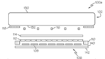
도 1을 참조하여 보면, 터치 스크린 어셈블리(100)의 탑 뷰(top view)를 개락적으로 나타낸다. 상기 터치 스크린 어셈블리(100)는 일반적으로 다수의 터치 민감 센서(104)를 포함한다. 상기 터치 민감 센서(104)는 열 전극 (116) 및 행 전극(115)의 교차점에 형성되고, 이들 전극은 이온-교환 강화된 밀봉 유리(102)의 상단 표면 또는 밑면에 형성된다. 상기 전극(115, 116)은 밀봉 유리(102)의 동일한 면 또는 밀봉 유리(102)의 반대 면에 형성될 수 있다, 밀봉 유리(102)는 교대로 이온-교환가능한 유리를 포함하는 뒤판 유리에 직접적으로 결합 및 밀봉된다. 본 명세서에서 상기 뒤판 유리가 이온-교환가능한 유리로부터 형성되는 것으로 기술되나, 상기 뒤판 유리가 이온-교환 강화될 필요는 없다. 따라서, 본 명세서에서 기술된 터치 스크린 어셈블리의 구체예에서, 뒤판 유리는 이온-교환 강화된 유리 또는 택일적으로, 비-이온-교환 강화된 유리일 수 있다.Referring to FIG. 1, the top view of the
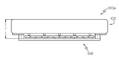
도 2a 및 2b를 참조하여 보면, 터치 스크린 어셈블리(100a)의 일 구체예의 분해 조립도(도 2a) 및 어셈블리 (도 2b)를 개략적으로 나타낸다. 본 명세서에 기술된 터치 스크린 어셈블리의 모든 구체예에서, 터치 스크린 어셈블리는 도 2a 및 2b에서 나타난 바와 같이, 프릿 밀봉(110)으로 뒤판 유리(106)에 직접 결합 및 밀봉되는 밀봉 유리(102)를 포함한다. 상기 밀봉 유리(102)는 알칼리-알루미노 실리케이트 유리와 같은 이온-교환 강화된 유리로부터 형성된다. 적절한 이온-교환 강화된 유리의 예는 코닝에 의해 제조된 이온-교환 강화된 GorillaTM Glass 및 GorillaTM Glass 2를 포함하나 이에 한정되지 않는다. 그러나, 다른 이온-교환 강화된 유리가 상기 밀봉 유리(102)에 사용될 수 있다. 상기 밀봉 유리(102)는 상단 표면(130) 및 밑면(132)을 포함하고 각각의 상단 표면 및 밑면은 이온 교환 강화에 의해 밀봉 유리(102)에 주는 압축 응력 층을 포함한다. 상기 압축 응력은 밀봉 유리(102)의 상단 표면(130) 및 밑면(132) 모두에서부터 밀봉 유리의 두께까지 이다. 상기 압축 응력은 밀봉 유리의 기계적인 강도를 향상시키고 일반적으로 부수적인 손상(예를 들면, 칩(chip), 스크래치 등)때문에 밀봉 유리의 실패를 경감시킨다. 본 명세서에 기술된 구체예에서, 밀봉 유리(102)의 압축 응력은 약 500 ㎫ 이상이고, 층 깊이(DOL)는 약 30㎛ 이상이다. 예를 들면, 여러 구체예에서, 상기 압축 응력은 800 ㎫ 이상 또는 심지어 950 ㎫ 이상일 수 있다. 여러 구체예에서, DOL은 약 40 ㎛ 이상이거나 심지어 약 50㎛ 이상일 수 있다. 상기 압축 응력 및 DOL은 ASTM 표준 C1422에서 기술된 대로 유리의 응력 복굴절(stress birefringence)에 기초하여 결정된다.Referring to Figures 2a and 2b, there is shown schematically an exploded assembly view (Figure 2a) and an assembly (Figure 2b) of an embodiment of
본 명세서에 기술된 구체예에서, 상기 밀봉 유리(102)는 약 1㎜ 이하의 두께 T1를 일반적으로 갖는다. 예를 들면, 상기 밀봉 유리(102)는 약 0.5㎜ 내지 약 1㎜범위의 두께 T1를 가질 수 있다. 예를 들면, 상기 밀봉 유리(102)는 약 0.5㎜ 내지 약 0.7㎜범위의 두께 T1를 가질 수 있다. 일 대표적인 구체예에서, 상기 밀봉 유리(102)는 약 0.55㎜의 두께 T1를 가진다. 또 다른 대표적인 구체예에서, 상기 밀봉 유리(102)는 약 0.7㎜의 두께 T1를 가진다.In the embodiment described herein, the sealing
더욱이, 상기 밀봉 유리(102)는 제 1 열 팽창 계수 CTE1을 가진다. 구체예에서, 상기 밀봉 유리가 알칼리-알루미노 실리케이트 유리인 경우에, CTE1는 약 75x10-7/℃ 내지 약 100x10-7/℃ 범위이다. 일 구체예에서, CTE1는 약 80x10-7/℃ 내지 약 85x10-7/℃ 범위이다. 예를 들면, 상기 밀봉 유리(102)가 GorillaTM Glass로부터 형성되는 경우, CTE1는 0℃로부터 약 300℃까지 대략 84.5x10⁻⁷/℃이다. 택일적으로, 상기 밀봉 유리(102)가 GorillaTM Glass 2로부터 형성되는 경우, CTE1는 0℃로부터 약 300℃까지 대략 80x10-7/℃이다.Furthermore, the sealing
상기 뒤판 유리(106)는 알칼리 알루미노 실리케이트 유리와 같은 이온-교환가능한 유리로부터 형성되고, 이는 프릿 밀봉(110)으로 밀봉 유리(102)와 뒤판 유리(106)의 결합 및 밀봉을 용이하게 하기 위하여 뒤판 유리의 열팽창 계수는 밀봉 유리(12)의 열팽창 계수와 유사한 값을 가진다. 구체적으로, 뒤판 유리(106)와 밀봉 유리(102) 사이의 밀폐된 프릿 밀봉의 무결성(integrity)을 유지하기 위하여, 운전 동안 터치 스크린 어셈블리(100)의 온도가 변화함에 따라 뒤판 유리(106)와 밀봉 유리(102)는 뒤판 유리(106)와 밀봉 유리(102) 사이의 팽창 차이를 최소화하도록 뒤판 유리(106)와 밀봉 유리(102)는 유사한 열 팽창 계수를 가진다. 따라서, 본 명세서에서 기술된 구체예에서, 뒤판 유리(106)는 일반적으로 밀봉 유리(102)의 열 팽창 계수와 유사한 제 2 열팽창 계수 CTE2를 가지는 이온-교환가능한 유리를 포함한다. 구체적으로, 뒤판 유리(106)는 CTE2가 CTE1의 +/- 15.0x10⁻⁷/℃ 범위 내 또는 심지어 CTE1의 +/- 10.0x10⁻⁷/℃ 범위 내 가 되도록 제 2 열팽창 계수 CTE2를 가진다. 예를 들면, 일 구체예에서, 뒤판 유리(106)의 CTE2는 밀봉 유리(102)의 CTE1과 동일하다(즉, CTE2 = CTE1). 따라서, 위에서 기술한 바와 같이, 밀봉 유리가 알칼리 알루미노 실리케이트 유리로부터 형성되는 경우, CTE2가 CTE1과 유사 또는 동일하도록 뒤판 유리(106)의 CTE2는 일반적으로 약 75x10-7/℃ 내지 약 100x10-7/℃ 범위 또는 심지어 약 80x10-7/℃ 내지 약 85x10-7/℃ 범위임이 이해될 것이다. 여러 구체예에서, 뒤판 유리(106)와 밀봉 유리(102)는 뒤판 유리(106)와 밀봉 유리(102) 사이의 팽창 차이를 최소화하도록 뒤판 유리(106)와 밀봉 유리(102)는 동일한 조성을 갖는 유리로부터 형성된다. 여기서 사용된 "동일한 조성"이란 밀봉 유리가 이온-교환 강화되기 전에 뒤판 유리(106)의 조성과 밀봉 유리(102)의 조성을 의미한다. 따라서, 이들 구체예에서, 뒤판 유리(106)의 조성은 뒤판 유리(106)가 이온 교환에 의해 유리내 도입되는 이온을 포함하지 않는다는 점에서 터치 스크린 어셈블리(100)내 밀봉 유리(102)의 조성과 다르다는 것이 이해될 것이다. 더욱이, 다른 구체예에서, 뒤판 유리(106)와 밀봉 유리(102)는 동일한 조성을 가진 유리로 형성될 필요가 없다는 것이 또한 이해될 것이다.The
"이온 교환가능한 유리"라는 용어는 뒤판 유리(106)를 기술하고 유리의 표면에 압축 응력을 형성하도록 용융된 염욕의 더 큰 알칼리 이온(예를 들면, 포타슘 이온)을 유리 내의 더 작은 알칼리 이온(예를 들면, 소디윰 이온)으로 이온교환하기 쉽게 하기 위하여 알칼리 이온을 함유한 용융된 염욕에 유리를 담지시켜 유리가 이온-교환 강화될 수 있음을 의미한다. 그러나, 뒤판 유리(106)의 물리적 물성(구체적으로 뒤판 유리의 CTE)이 밀봉 유리(102)의 물리적 물성과 유사하도록 이온-교환 강화가 가능할 뿐 반드시 뒤판 유리는 이온-교환 강화될 필요가 없음이 이해될 것이다.The term "ion-exchangeable glass" describes the
따라서, 여러 구체예에서, 뒤판 유리(106)는 이온-교환가능한 유리이나 다른 구체예에서는 이온-교환 강화되지 않고, 상기 뒤판 유리는 또한 이온-교환 강화된 이온-교환가능 유리이다. 이온-교환 강화되지 않은 이온-교환가능한 유리의 적절한 예는 유리가 이온 교환에 노출되기 전에 코닝에 의해 제조된 GorillaTM Glass 및 GorillaTM Glass 2로서 동일한 조성을 가진 유리를 포함하나 이에 한정되지 않는다. 이온-교환 강화된 이온-교환가능한 유리의 적절한 예는 코닝에 의해 제조된 GorillaTM Glass 및 GorillaTM Glass 2를 포함하나 이에 한정되지 않는다.Thus, in various embodiments, the
뒤판 유리(106)가 이온-교환 강화된 실시예에서, 뒤판 유리(106)의 압축 응력이 일반적으로 밀봉 유리(102)의 압축 응력보다 더 작고, 뒤판 유리(106)의 DOL이 일반적으로 밀봉 유리(102)의 DOL보다 더 작도록 뒤판 유리(106)는 약간 이온 교환 강화된다. 이들 구체예에서, 뒤판 유리내 압축 응력은 약 600㎫ 이상이고 약 40㎛이하의 층 깊이(DOL)를 가진다. 여러 구체예에서, 상기 DOL은 약 35㎛이하 또는 심지어 약 30㎛이하일 수 있다.In an embodiment in which the
본 명세서에 기술된 구체예에서, 밀봉 유리(102)의 두께 T1은 일반적으로 뒤판 유리(106)의 두께 T2보다 크고, 밀봉 유리(102)는 주로 터치 스크린 어셈블리(100)에 기계적 강도를 주는데 책임이 있다. 따라서, 뒤판 유리(106)는 밀봉 유리(102)에 비하여 상당히 얇을 수 있다. 뒤판 유리(106)의 두께 T2는 일반적으로 약 0.5 mm미만이다. 예를 들면, 여러 구체예에서, 뒤판 유리(106)는 약 0.4mm이하 또는 약 0.3mm이하일 수 있다. 다른 구체예에서, 뒤판 유리(106)는 약 0.2mm이하 또는 약 0.1mm이하일 수 있다.The thickness T 1 of the sealing
도3a 및 도 3b를 참조하여 보면, 뒤판 유리(106)는 MO-TFTs의 어레이에 증착된 밑면(142) 및 장치 표면(140)을 포함한다. 여러 구체예에서, 뒤판 유리(106)는 장치 표면(140) 및 선택적으로 밑면(142)은 알칼리 이온이 없도록 형성된다. 구체적으로, 장치 표면(140)의 알칼리 이온은 MO-TFT 어레이에 잠재적으로 손상을 주는 장치 표면(140)에 증착된 MO-TFTs의 어레이에 이동하거나 용해될 수 있다. 따라서, 이러한 손상을 방지하기 위하여 적어도 장치 표면(140)은 알칼리 이온이 없을 수 있다.Referring to Figures 3A and 3B,
도 3a를 참조하여 보면, 일 구체예에서, 뒤판 유리(106)는 장치 표면(140)에 형성된 알칼리 프리 존(alkali free zone 150)을 포함한다. 이와 유사하게, 알칼리 프리 존(150, 152) 사이에 알칼리 함유 코어(154)가 위치되도록 알칼리 프리 존(150)은 뒤판 유리(106)의 밑면(142)에 형성될 수 있다. 이러한 구체예에서, 예를 들면, 고체의 암모늄 술페이트 염 또는 암모늄 술페이트 염 용액과 같은 탈알칼리화제(dealkalizing agent)에 하나 이상의 뒤판 유리 표면을 노출시켜 알칼리 프리 존(150, 152)은 뒤판 유리(106)를 탈알칼리시켜 형성될 수 있다.Referring to FIG. 3A, in one embodiment, the
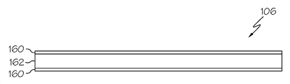
도 3b를 참조하여 보면, 또 다른 구체예에서, 뒤판 유리(106)는 밑면 및 장치 표면이 알칼리 이온이 없도록 적층된 유리 구조물로부터 형성될 수 있다. 이러한 구체예에서, 알칼리 함유 코어(162)가 알칼리-프리 클래딩 유리(alkali-free cladding glass, 160)의 두 층 사이에 적층된다. 알칼리 함유 코어(162)는 상기 기술한 바와 같이 알칼리-알루미노 실리케이트 유리로부터 형성되나, 클래딩 유리(160)는 예를 들면 코팅으로부터 제조된 EagleTM glass와 같은 알칼리-프리 유리로부터 형성된다. 이러한 적층은 예를 들면 본 명세서에 참조로서 혼입되는 미국 특허 번호 제4,214,886호에 개시된 더블-퓨전 드로잉 공정을 포함하는 다양한 다른 공정으로부터 형성될 수 있다. 이러한 구체예에서, 전반적인 CTE가 여전히 밀봉 유리(102)의 CTE과 양립가능하도록 적층된 구조물의 CTE는 클랭딩 유리의 CTE와 코어 유리의 CTE 사이의 중간값이다. 알칼리 함유 코어(162)가 두 알칼리-프리 클래딩 유리(160) 사이에 배치되기 때문에 적층된 구조물은 이온 교환가능하지 않다. 그러나, 코어 유리가 이온 교환 가능하게 만드는 알칼리 이온을 함유하기 때문에, 적층된 구조물이 전체적으로 이온 교환가능하지 않을지라도 적층된 구조물은 필연적으로 이온 교환가능한 유리를 포함한다.Referring to FIG. 3B, in another embodiment, the
도 2a 및 2b를 참조하여 보면, 밀봉 유리(102) 및 뒤판 유리(106)의 이온-교환 강화된 유리의 사용은 터치 스크린 어셈블리(100a)의 뒤판 유리(106)에 증착된 MO-TFTs의 어레이의 사용에 의해 가능하게 된다. 구체적으로, 상기 MO-TFTs는 실리콘계 TFTs보다 크고 밀봉 유리(102) 및 뒤판 유리(106)의 열 팽창 계수와 더 유사한 제 3 열 팽창 계수 CTE3를 가진다. MO-TFTs의 열 팽창 계수는 MO-TFTs의 두께에 따라 변하고, MO-TFTs의 열 팽창 계수는 뒤판 유리(106)의 열 팽창 계수와 동일 또는 실질적으로 유사하게 "조절"될 수 있다. 본 명세서에 기술된 여러 구체예에서, CTE3 는 CTE2의 +/- 15.0x10⁻⁷/℃ 범위 내이거나 심지어 +/- 10.0x10⁻⁷/℃ 범위 내이다. 여러 구체예에서, MO-TFTs의 어레이(108)는 인듐 갈륨 아연 산화물(IGZO)로부터 형성된다. 여러 다른 구체예에서, MO-TFTs의 어레이(108)는 아연 산화물로부터 형성된다. 뒤판 유리(106) 및 밀봉 유리(102)와 유사한 열 팽창 계수를 갖는 MO-TFTs의 사용은 제조 및 후속 사용 동안 이들 구성성분 사이의 팽창 차이를 최소화하고 그 결과 운전 동안 팽창으로 더 많은 차이를 일으키는 다양한 구성성분의 조정불량에 기인한 디스플레이 성능 감소 및/또는 TFTs의 손상을 최소화한다.2A and 2B, the use of the ion-exchange enhanced glass of the sealing
본 명세서에서 기술한 구체예에서, MO-TFTs의 어레이(108) 및 관련 구성성분(예를 들면, OLED 장치의 어레이 등)은 뒤판 유리(106)의 장치 표면(140)에 위치되고 밀봉 유리(102)의 밑면(132)과 뒤판 유리(106)의 장치 표면(140) 사이에 다양한 성분이 밀봉되도록 하는 프릿 밀봉(11)에 의해 결합되는 장치 영역 안에 위치된다. 본 명세서에서 기술한 구체예에서, 프릿 밀봉(11)은 분말화된 유리 프릿으로부터 형성되고, 이는 소결되는 경우, 온도 유동의 결과로서 프릿 밀봉의 실패경감을 위하여 밀봉 유리(102) 및 뒤판 유리(106)의 열 팽창 계수와 유사한 열 팽창 계수를 가진다.In an embodiment described herein, the
도 2a 및 2b에서 나타낸 터치 스크린 어셈블리의 구체예를 참조하여, 상기 터치 스크린 어셈블리(100a)는 OLED 장치의 어레이(112)를 추가로 포함하고, 이는 MO-TFTs의 어레이(108)에 걸쳐서 형성되고, OLED 장치의 어레이내에서 각각의 OLED가 MO-TFTs의 어레이내 상응하는 트랜지스터로 스위치 온 및 오프되도록 전자적으로 MO-TFTs의 어레이와 결합된다. 도 2a 및 2b에 개략적으로 나타낸 터치 스크린 어셈블리의 구체예에서, 각각의 그룹의 RGB OLED 장치가 OLED 디스플레이의 픽셀을 형성하도록 OLED 장치의 어레이(112)는 상부 방출(top emitting) 레드, 그린 및 블루(RGB) OLED 장치의 어레이를 포함한다.2a and 2b, the
OLED 장치의 어레이가 상부 방출 RGB OLED 장치를 포함하는 것으로 본 명세서에 기술되었으나, 이는 다른 구성을 고려하는 것으로 이해되어야 한다. 예를 들면, 개별적인 레드, 그린 및 블루 방출 OLED 장치를 이용하는 OLED 디스플레이에서, 다른 컬러 OLEDs의 차이 에이징(differential aging)은 디스플레이의 수명에 걸쳐 컬러 시프트의 결과를 초래할 수 있다. 게다가, 이러한 OLED 디스플레이의 형성은 다르게 컬러화된 OLED 물질의 디포지션(deposition)을 용이하게 하기 위하여 다수의 쉐도우 마스크의 이용을 필요로 할 수 있어 그 결과 제조 공정의 복잡성이 추가된다. 따라서, 대안적인 구체예에서(도시되지 않음), OLED 장치의 어레이는 상부 방출 화이트 OLED 장치로 이루어지고, 이는 분리된 레드, 그린 및 블루 OLED 장치를 사용하는 것과 연관된 문제점을 피한다. 이러한 구체예에서, 개별적으로 디스플레이된 픽셀에 컬러를 제공하기 위하여 컬러 필터는 밀봉 유리의 밑면에 위치될 수 있다.Although an array of OLED devices is described herein as including a top emission RGB OLED device, it should be understood that this considers other configurations. For example, in an OLED display using discrete red, green, and blue emitting OLED devices, differential aging of different color OLEDs may result in a color shift over the lifetime of the display. In addition, the formation of such an OLED display may require the use of multiple shadow masks to facilitate the deposition of differently colored OLED materials, which adds to the complexity of the manufacturing process. Thus, in an alternative embodiment (not shown), the array of OLED devices consists of a top emission white OLED device, which avoids the problems associated with using separate red, green and blue OLED devices. In this embodiment, the color filter may be located on the underside of the sealing glass to provide color to the individually displayed pixels.
다른 대안적인 구체예에서(도시되지 않음), OLED 장치의 어레이는 분리된 레드, 그린 및 블루 OLED 장치를 사용하는 것과 연관된 문제점을 피하기 위하여 상부 방출 블루 OLED 장치를 포함한다. 컬러의 디스플레이를 용이하게 하기 위하여, 상기 터치 스크린 어셈블리는 밀봉 유리의 밑면에 위치된 양자점(quantum dot) 서브-픽셀의 어레이를 추가로 포함할 수 있다. 상기 양자점 서브-픽셀은 금속화된 웰(well)에 위치되며, 이는 개별적인 서브-픽셀 사이의 크로스-토크(cross-talk)를 감소한다. 양자점 서브-픽셀의 어레이에서 각각의 서브-픽셀은 레드 및 그린 양자점 방출기 및 블루 라이트 스캐터(scattere)를 포함한다. 따라서, 이 구체예에서, OLED 장치의 어레이에 의해서 방출되는 블루 라이트는 빛이 양자점 서브-픽셀의 어레이를 통과하여 레드, 그린 또는 블루 라이트로 변환된다.In another alternative embodiment (not shown), the array of OLED devices includes a top emission blue OLED device to avoid the problems associated with using separate red, green, and blue OLED devices. To facilitate display of color, the touch screen assembly may further include an array of quantum dot sub-pixels located on the underside of the encapsulation glass. The quantum dot sub-pixels are located in a metallized well, which reduces cross-talk between the individual sub-pixels. Each sub-pixel in the array of quantum dot sub-pixels includes red and green quantum dot emitters and blue light scatterers. Thus, in this embodiment, the blue light emitted by the array of OLED devices is converted to red, green or blue light through an array of quantum dot sub-pixels.
더욱이, 본 명세서에 기술된 구체예에서, OLED 장치의 어레이(112)와 밀봉 유리(102)의 밑면(132) 사이의 공간의 다른 굴절 인덱스(refractive index)를 보상하기 위하여 인덱스-매칭 겔(114)(직사각형 블록으로 개략적으로 나타냄)은 OLED 장치의 어레이(112)와 밀봉 유리(102)의 밑면(132) 사이에 배치된다.Furthermore, in the embodiments described herein, an index-matching gel 114 (see FIG. 1) is used to compensate for a different refractive index of the space between the
본 명세서에 기술된 구체예에서, 터치 스크린 어셈블리는 다수의 터치 센서 전극을 추가적으로 포함한다. 도 2a-2b 및 4a-6b에서 나타낸 터치 스크린 어셈블리의 다양한 구체예에서, 터치 스크린 어셈블리는 밀봉 유리(102)의 밑면(132)에 증착되는 터치 센서 전극(116)을 이용한다. 이들 구체예에서, 터치 센서 전극은 인듐 주석 산화물(ITO)로부터 형성될 수 있다. 이 구체예에서, 행 및 열 전극 모두는 밀봉 유리(102)의 밑면(132)에 증착되고, 박막의 절연 물질은 행 및 열 전극 사이에 증착된다. 그러나, 다른 구체예에서(도시되지 않음), 공동 쌍의 터치 센서 전극은 상단 표면(130) 및 밀봉 유리(102)의 밑면(132)에 증착될 수 있다. 이들 구체예에서, 터치 센서 전극은 인듐 주석 산화물 또는 예를 들면, 알루미늄 아연 산화물과 같은 유사 물질로부터 형성될 수 있다.In the embodiments described herein, the touch screen assembly additionally includes a plurality of touch sensor electrodes. 2a-2b and 4a-6b, the touchscreen assembly utilizes a
여러 구체예에서, 터치 센서 전극(116)은 ITO로부터 형성된 전기통로(electrical traces)와 서로 연결될 수 있다. 다른 구체예에서, 터치 센서 전극(116)은 ITO 통로보다 실질적으로 더 얇은 (약 5㎛) 구리 또는 알루미늄과 같은 금속 물질로부터 형성된 전기통로로 서로 연결된다. 이들 구체예에서, 금속 통로는 밀봉 유리(102)의 밑면에 위치된 특히 이들 전기통로에 대한 정반사율(specular reflectance)을 감소시키기 위하여 블랙 크롬과 같은 블랙 마스크로 추가적으로 코팅될 수 있다.In various embodiments, the
도 2a 및 2b를 참조하여 보면, 본 명세서에 기술된 터치 스크린 어셈블리의 구체예는 밀봉 유리(102)의 밑면(132) 및 프릿 밀봉(110) 사이에 배치된 주위 프릿(perimeter frit, 118)을 선택적으로 포함할 수 있다. 주위 프릿(118)은 주위 프릿(118)이 밀봉 유리(102)와 뒤판 유리(106)를 결합하고 밀봉할 뿐만 아니라 터치 스크린 어셈블리의 기본 구성요소를 모호하게 하도록 컬러화될 수 있다. 더욱 자세하게는, 통상적인 장치는 디스플레이 구멍(aperture)내에 있지 않은 터치 스크린 디스플레이 어셈블리의 모호한 부분에 유기 잉크를 일반적으로 사용한다. 그러나, 어셈블리의 제조 동안, 이들 잉크는 특히, 프릿 밀봉(110)의 레이저 공정 동안 쉽게 손상된다. 그러므로, 밀봉 및 장식적인 꾸밈으로 기능하는 주위 프릿(118)은 유기 잉크의 대안으로서 사용될 수 있다.2A and 2B, an embodiment of the touch screen assembly described herein includes a
주위 프릿(118)을 이용한 구체예에서, 터치 센서 전극과 연결된 금속 통로가 주위 프릿(118) 및 프릿 밀봉(110) 사이에 배치되는 금속 회수관(return lines)과 서로 연결되도록 주위 프릿(118)과 교차하기 때문에 주위 프릿(118)은 얇아야만 한다(예를 들면, 10㎛ 미만).In embodiments using the
도 4a 및 4b를 참조하여 보면, 터치 스크린 어셈블리(100)의 또 다른 구체예를 개략적으로 나타낸다. 이 구체예에서, 터치 스크린 어셈블리(100b)는 도 2a 및 2b에서 상기 기술한 바와 같이, 밀봉 유리(102), 뒤판 유리(106), 프릿 밀봉(110), MO-TFTs의 어레이(108), 인덱스-매칭 겔(114), 및 다수의 터치 센서 전극(116)을 포함한다. 그러나, 이 구체예에서, 터치 스크린 어셈블리는 원형 편광기(circular polarizer, 120)를 추가적으로 포함한다. 상기 원형 편광기는 다수의 터치 센서 전극(116)이 원형 편광기(120) 및 밀봉 유리(102)의 밑면 사이에 위치되도록 밀봉 유리(102)의 밑면(132)에 붙는다. 원형 편광기(120)는 약 100㎛ 두께를 가지고, 이는 프릿 밀봉(110)의 증가되는 두께를 원형 편광기의 추가된 두께를 위한 충분한 공간을 제공하는데 필요하다.Referring now to Figures 4A and 4B, another embodiment of
그러나, 프릿 밀봉(110)의 증가되는 두께는 프릿 밀봉(110)의 불완전한 처리, 궁극적으로는 밀봉 실패를 유발할 수 있다. 그러므로, 어떤 구체예에서, 유리 스페이서 프레임(glass spacer frame, 122)은 필러 물질과 같이 행동하기 위하여 뒤판 유리(106)의 주의를 따라 위치될 수 있다. 유리 스페이서 프레임(122)은 유리 스페이서 프레임(122)이 뒤판 유리(106)에 위치하는 경우, 뒤판 유리(106)의 장치 표면이 유리 스페이서 프레임을 통하여 노출되도록 열린 중앙 영역(125)을 갖는 연속적인 외부 경계를 가진다(도 5). 유리 스페이서 프레임(122)은 프릿 밀봉(123)으로 뒤판 유리(106)에 밀봉되고 프릿 밀봉(110)으로 밀봉 유리(102)에 밀봉된다. 유리 스페이서 프레임(122)의 포함은 원형 편광기(120)의 추가를 수용하고, 터치 스크린 어셈블리의 바람직한 밀봉을 유지한다. 본 명세서에 기술된 구체예에서, 유리 스페이서 프레임(122)은 CTE2의 +/- 15.0x10⁻⁷/℃ 범위내 또는 심지어 CTE2의 +/- 10.0x10⁻⁷/℃ 범위내인 열 팽창 계수 CTEf 를 가진 유리로부터 형성된다.However, the increased thickness of the
터치 스크린 어셈블리(100b)가 원형 편광기(120)를 포함하는 구체예에서, 행 또는 열 터치 센서 전극은 밀봉 유리(102)의 밑면(132)에 형성될 수 있는데 반하여, 상기 상보적인 터치 센서 전극(즉, 열 또는 행 전극)은 편광기의 밑면(즉, 뒤판 유리(106)와 마주보는 원형 편광기(120)의 표면)에 형성될 수 있다. 이 구체예에서, 상기 편광기는 행 및 열 터치 스크린 전극 사이에 절연체처럼 행동한다.In embodiments where the
도 2a 및 2b를 다시 참조하여 보면, 터치 스크린 어셈블리의 구체예에서, 뒤판 유리(106)의 장치 표면(140)상에 MO-TFTs의 어레이가 증착되어 형성될 수 있다. 마스크가 장치 표면(140)에 처음으로 적용되어 MO-TFTs의 어레이(108)를 정의하고 상기 MO-TFT물질은 플라즈마 개선된 화학 기상 증착(plasma enhanced chemical vapor deposition (PECVD)) 및 스퍼터링을 사용하여 진공하에서 증착된다. 상기 MO-TFT물질이 증착된 후, 상기 마스크는 장치 표면으로부터 제거된다.Referring again to Figures 2A and 2B, in an embodiment of the touch screen assembly, an array of MO-TFTs may be deposited and formed on the
OLED 장치의 어레이(112)가 전기적으로 MO-TFTs의 어레이(108)와 결합되도록 OLED 장치의 어레이(112)는 그 다음 MO-TFTs의 어레이(108)에 증착된다. OLED 장치의 어레이(112)는 진공 열 증착 기술을 사용하여 MO-TFTs에 증착될 수 있다.The
선택적인 주위 프릿(118)을 포함하는 터치 스크린 어셈블리의 구체예에서, 주위 프릿은 밀봉 유리의 밑면(132)에 페이스트(paste)로서 증착되고, 그 후, 밀봉 유리(102)는 주위 프릿(118)을 경화시키기 위하여 굽는다. 분리된 단계에서, 터치 센서 전극(116)은 스퍼터링 및/또는 프린터링에 의하여 밀봉 유리(102)의 밑면(132) 및 (선택적으로) 상단 표면(130)에 증착된다.In an embodiment of the touch screen assembly that includes the optional
상기 기술한 바와 같이, 터치 스크린 어셈블리의 여러 구체예는 선택적으로 밀봉 유리의 밑면에 위치된 컬러 필터를 이용할 수 있다. 이들 구체예에서, 상기 컬러 필터 물질은 스핀 기술 또는 닥터 블레이드 기술을 이용하여 터치 센서 전극 전체에 증착된다. 컬러 필터 물질의 적용 후에, 상기 물질은 오븐에서 경화된다.As described above, various embodiments of the touch screen assembly may optionally utilize color filters located on the underside of the seal glass. In these embodiments, the color filter material is deposited over the touch sensor electrode using a spin technique or a doctor blade technique. After application of the color filter material, the material is cured in an oven.
더욱이, 도 4a-4b에서 나타낸 바와 같이 원형 편광기(120)를 포함하는 구체예에서, 터치 센서 전극(116)이 원형 편광기(120) 및 밀봉 유리(102)의 밑면(132) 사이에 위치되도록 원형 편광기(120)는 밀봉 유리(102)의 밑면(132)에 붙는다(도 4a-4b).Furthermore, in embodiments including the
도 4a-4b에서 나타낸 바와 같이 원형 편광기(120)를 포함하는 구체예에서, 프릿 페이스트의 비드는 유리 스페이서 프레임(122)에 적용되고, 유리 스페이서 프레임(122)은 유리 스페이서 프레임(122)의 밑면에 적용되며, 상기 유리 스페이서 프레임(122)은 프릿 페이스트가 유리 스페이서 프레임(122)과 뒤판 유리(106) 사이에 배치되도록 뒤판 유리(106)의 장치 표면(140)에 위치된다. 그 후, 프릿 페이스트는 상기 프릿 페이스트를 고형화하도록 하나 또는 모두의 유리 스페이서 프레임(122) 또는 뒤판 유리(106)를 통하여 레이저 빔을 겨냥하여 조사하여 상기 스페이서 프레임(122)과 뒤판 유리(106)를 결합 및 밀봉한다.4A-4B, the bead of the frit paste is applied to a
다양한 구성성분이 밀봉 유리(102)의 밑면(132) 및 뒤판 유리(106)의 장치 표면(140)에 형성될 때, 프릿 페이스트는 뒤판 유리(106)의 장치 표면(140)의 주위에 적용된다. 유리 스페이서 프레임이 이용되는 구체예에서, 프릿 페이스트는 유리 스페이서 프레임의 상단 표면에 적용된다. 유리 스페이서 프레임이 이용되지 않는 구체예에서, 프릿 페이스트는 뒤판 유리(106)의 장치 표면(140)에 직접적으로 적용된다. 인덱스-매칭 겔(114)은 뒤판 유리의 장치 표면(140)에 증착된 구성성분에 걸쳐서 위치된다. 그 후에, 밀봉 유리(102)는 뒤판 유리(106)와 나란히 하고 상기 어셈블리는 진공하에 놓인다. 상기 프릿 페이스트는 상기 프릿 페이스트를 고형화하도록 하나 또는 모두의 밀봉 유리(102) 또는 뒤판 유리(106)를 통하여 레이저 빔을 겨냥하여 조사하여 상기 밀봉 유리(102)와 뒤판 유리(106)를 결합 및 밀봉한다.The frit paste is applied around the
본 명세서에 기술된 터치 스크린 어셈블리의 구체예에서, 터치 스크린 어셈블리는 2mm 미만 또는 심지어 1.5mm미만의 두께 T를 가질 수 있다. 예를 들면, 여러 구체예에서, 터치 스크린 어셈블리의 두께 T는 1mm이하일 수 있다. 이러한 터치 스크린 어셈블리는 다양한 전자 장치내에 쉽게 혼입될 수 있고, 어셈블리의 감소된 두께때문에 특히 휴대가능한 전자 장치에 매우 적합하다.In embodiments of the touch screen assembly described herein, the touch screen assembly may have a thickness T of less than 2 mm or even less than 1.5 mm. For example, in various embodiments, the thickness T of the touch screen assembly may be less than or equal to 1 mm. Such a touch screen assembly can be easily incorporated into a variety of electronic devices and is particularly well suited for portable electronic devices because of the reduced thickness of the assembly.
도 6을 참조하여 보면, 터치 스크린 어셈블리(100e)의 일 구체예를 개략적으로 나타낸다. 이 구체예에서, 밀봉 유리(102)는 반경의 굴곡으로 형성되나 뒤판 유리(106)는 처음에 평면이다. 다양한 구성성분의 터치 스크린 어셈블리가 밀봉 유리(102) 및 뒤판 유리(106)에 증착될 때, 터치 스크린 어셈블리(100e)가 반경의 굴곡이 되도록 밀봉 공정 동안 상기 어셈블리에 압력을 인가하여 뒤판 유리(106)는 밀봉 유리(102)의 형태에 따른다.Referring to FIG. 6, there is shown schematically one embodiment of
본 명세서에 기술된 터치 스크린 어셈블리가 기계적인 강도 및 손상 내성이 향상되고 또한, 종래의 터치 스크린 패널에 비하여 감소된 두께를 가짐이 이해될 것이다. 상기 향상된 기계적 물성 및 감소된 두께는 이온-교환가능한 뒤판 유리에 직접 결합되는 이온-교환 강화된 밀봉 유리를 사용하여 달성된다. 이온-교환 강화된 및 이온-교환가능한 유리의 사용은 밀봉 유리, 뒤판 유리 및 MO-TFTs의 열 팽창 계수가 유사하도록 뒤판 유리에 MO-TFTs의 사용이 용이하게 되어, 공정 및 후속 사용 동안 물질들 사이에 팽창 차이를 감소시킨다.It will be appreciated that the touch screen assembly described herein improves mechanical strength and damage resistance and also has a reduced thickness compared to conventional touch screen panels. The improved mechanical properties and reduced thickness are achieved using an ion-exchange strengthened sealing glass that is directly bonded to the ion-exchangeable backing glass. The use of ion-exchange enhanced and ion-exchangeable glasses facilitates the use of MO-TFTs in backing glass so that the thermal expansion coefficients of the sealing glass, backing glass and MO-TFTs are similar, Thereby reducing the expansion difference.
더욱이, 터치 스크린 어셈블리의 향상된 기계적 물성 및 감소된 두께때문에, 상기 터치 스크린 어셈블리는 다양한 전자 장치에의 사용이 보다 적합하고, 특히 휴대가능한 전자 장치에 사용에 적합하다. 더욱이, 본 명세서에 기술된 터치 스크린 어셈블리의 뒤판 유리는 종래의 평면 어셈블리에서 벗어난 터치 스크린 어셈블리의 생산을 용이하게 하는 밀봉 유리보다 상당히 더 얇을 수 있어 디자인에서 전자 장치 제조자들이 더 유연성 있게 적용할 수 있다.Moreover, due to the improved mechanical properties and reduced thickness of the touch screen assembly, the touch screen assembly is more suitable for use in various electronic devices, and is particularly suitable for use in portable electronic devices. Moreover, the backing glass of the touchscreen assembly described herein can be considerably thinner than a sealing glass that facilitates production of a touchscreen assembly that deviates from conventional planar assemblies, making it more flexible for electronic device manufacturers in design .
당업자는 본 발명의 범위를 벗어나지 않고 본 명세서에서 기술한 구체예를 다양한 수정 및 변형을 만들 수 있다. 그러므로, 본 명세서는 본 명세서에서 기술된 다양한 구체예의 수정 및 변형을 모두 포함하고, 이러한 수정 및 변형은 본 발명의 청구항 및 이의 균등 범위내에 모두 포함된다. Those skilled in the art can make various modifications and variations to the embodiments described herein without departing from the scope of the present invention. Therefore, the specification includes all modifications and variations of the various embodiments described herein, and such modifications and variations are all included within the scope of the claims of the invention and its equivalents.
Claims (20)
장치 표면, 밑면 및 제 2 열팽창 계수 CTE2를 갖는 이온-교환 강화된 유리를 포함하는 뒤판 유리, 여기서, CTE2는 CTE1의 +/- 15.0x10⁻⁷/℃ 범위내이고, 뒤판 유리의 장치 표면 및 밀봉 유리의 밑면 사이에 장치 영역을 밀봉시키는 프릿 밀봉으로 상기 뒤판 유리의 장치 표면이 밀봉 유리의 밑면에 결합 및 밀봉됨;
장치 영역에서 뒤판 유리의 장치 표면에 증착된 금속 산화물 박막 트랜지스터의 어레이; 및
뒤판 유리의 장치 표면에 장치 영역내 금속 산화물 박막 트랜지스터의 어레이에 걸쳐 형성된 OLED 장치 어레이;를 포함하는 전자 장치용 터치 스크린 어셈블리.The first thermal expansion coefficient CTE 1 And an ion-exchange strengthened glass having at least a plurality of touch sensor electrodes formed on a bottom surface of the sealing glass opposite the surface of the sealing glass;
Glass back plate, where, CTE 2 is +/- 15.0x10 -7 / ℃ range, and the device of the back plate of glass CTE 1 comprising a glass reinforced exchange-unit surface, the underside and the ion having the second coefficient of thermal expansion CTE 2 The device surface of the backing pane is bonded and sealed to the bottom surface of the sealing glass with a frit seal sealing the device area between the surface and the bottom surface of the sealing glass;
An array of metal oxide thin film transistors deposited on the device surface of the backing pane in the device region; And
An OLED device array formed over the array of metal oxide thin film transistors in the device region on the device surface of the backing pane.
상기 밀봉 유리는 적어도 30㎛의 층 깊이 및 500㎫ 이상의 압축 응력을 가지는 전자 장치용 터치 스크린 어셈블리.The method according to claim 1,
Wherein the sealing glass has a layer depth of at least 30 占 퐉 and a compressive stress of at least 500 MPa.
상기 금속 산화물 박막 트랜지스터의 어레이는 CTE2의 +/- 15.0x10⁻⁷/℃ 범위내인 제 3 열팽창 계수 CTE3를 가지는 전자 장치용 터치 스크린 어셈블리.The method according to claim 1,
The metal oxide thin film transistor array of the touch screen assembly for an electronic device having a +/- 15.0x10 -7 / ℃ within the range of the third coefficient of thermal expansion CTE of the third CTE 2.
상기 금속 산화물 박막 트랜지스터의 어레이는 CTE2의 +/- 10.0x10⁻⁷/℃ 범위내인 제 3 열팽창 계수 CTE3를 가지는 전자 장치용 터치 스크린 어셈블리.The method according to claim 1,
The metal oxide thin film transistor array of the touch screen assembly for an electronic device having a +/- 10.0x10 -7 / ℃ within the range of the third coefficient of thermal expansion CTE of the third CTE 2.
상기 밀봉 유리는 약 0.5㎜ 내지 약 0.7㎜의 제 1 두께 T1를 가지고, 상기 뒤판 유리는 약 0.1㎜ 이하의 제 2 두께 T2를 가지는 전자 장치용 터치 스크린 어셈블리.The method according to claim 1,
Wherein the sealing glass has a first thickness T 1 of about 0.5 mm to about 0.7 mm and the backing glass has a second thickness T 2 of about 0.1 mm or less.
CTE2는 CTE1의 +/- 10.0x10⁻⁷/℃ 범위내인 전자 장치용 터치 스크린 어셈블리.The method according to claim 1,
CTE 2 is within +/- 10.0 x 10 -7 / ° C of CTE 1 .
CTE1과 CTE2가 동일한 전자 장치용 터치 스크린 어셈블리.The method according to claim 1,
Touch screen assembly for electronic devices with the same CTE 1 and CTE 2 .
상기 밀봉 유리 및 뒤판 유리는 알칼리-알루미노 실리케이트 유리인 전자 장치용 터치 스크린 어셈블리.The method according to claim 1,
Wherein the sealing glass and backing plate glass are alkali-aluminosilicate glasses.
적어도 뒤판 유리의 장치 표면은 탈알칼리된 것인 전자 장치용 터치 스크린 어셈블리.The method according to claim 1,
Wherein at least the device surface of the backing pane is de-alkaline.
상기 뒤판 유리는 상기 뒤판 유리의 밑면 및 장치 표면이 알칼리-프리가 되도록 상부(upper) 및 하부(lower) 알칼리-프리 유리 클래딩 사이에 위치된 알칼리 함유 유리 코어를 포함하는 적층 유리인 전자 장치용 터치 스크린 어셈블리.The method according to claim 1,
The backing glass is a laminated glass comprising an alkali-containing glass core positioned between upper and lower alkali-free glass claddings such that the bottom surface of the backing plate glass and the device surface are alkali-free. Screen assembly.
다수의 터치 센서 전극이 원형 편광기 및 밀봉 유리의 밑면 사이에 위치되도록 밀봉 유리의 밑면에 부착된 원형 편광기를 더 포함하는 전자 장치용 터치 스크린 어셈블리.The method according to claim 1,
Further comprising a circular polarizer attached to an underside of the sealing glass such that a plurality of touch sensor electrodes are positioned between the bottom of the circular polarizer and the sealing glass.
뒤판 유리의 장치 표면에 밀봉된 유리 스페이서 프레임을 더 포함하는 전자 장치용 터치 스크린 어셈블리.The method of claim 11,
A touch screen assembly for an electronic device, further comprising a glass spacer frame sealed to the device surface of the backing pane.
밀봉 유리의 밑면의 주위에 인접하여 증착된 주위 프릿을 더 포함하고, 여기서, 주위 프릿은 밀봉 유리의 밑면 및 프릿 밀봉에 밀봉되는 전자 장치용 터치 스크린 어셈블리.The method according to claim 1,
Further comprising an ambient frit deposited adjacent the periphery of the bottom surface of the sealing glass, wherein the ambient frit is sealed to the bottom of the sealing glass and the frit seal.
밀봉 유리와 동일한 조성을 갖는 알칼리-알루미노 실리케이트 유리를 포함하는 뒤판 유리, 상기 뒤판 유리는 알칼리 이온이 없는 장치 표면 및 밑면을 가지고, 여기서, 뒤판 유리의 장치 표면 및 밀봉 유리의 밑면 사이에 장치 영역을 밀봉시키는 프릿 밀봉으로 상기 뒤판 유리의 장치 표면이 밀봉 유리의 밑면에 결합 및 밀봉됨;
장치 영역에서 뒤판 유리의 장치 표면에 증착된 금속 산화물 박막 트랜지스터의 어레이; 및
뒤판 유리의 장치 표면에 장치 영역내 금속 산화물 박막 트랜지스터에 걸쳐 형성된 OLED 장치의 어레이;를 포함하는 전자 장치용 터치 스크린 어셈블리.The first thermal expansion coefficient CTE 1 And an ion-exchange enhanced alkali-aluminosilicate glass having a plurality of touch sensor electrodes formed on at least a bottom surface of the sealing glass opposite the surface of the sealing glass;
A backing glass comprising an alkali-aluminosilicate glass having the same composition as the sealing glass, said backing glass having a device surface and an underside without an alkali ion, wherein a device area is provided between the device surface of the backing pane and the bottom surface of the sealing glass The device surface of the backing pane is bonded and sealed to the bottom surface of the sealing glass with a sealing frit seal;
An array of metal oxide thin film transistors deposited on the device surface of the backing pane in the device region; And
An array of OLED devices formed over the metal oxide thin film transistors in the device region on the device surface of the backing pane.
상기 뒤판 유리의 밑면 및 장치 표면은 탈알칼리된 전자 장치용 터치 스크린 어셈블리.15. The method of claim 14,
Wherein the underside of the backing plate and the device surface are de-alkaline.
상기 뒤판 유리는 상기 뒤판 유리의 밑면 및 장치 표면이 알칼리-프리가 되도록 상부 및 하부 알칼리-프리 유리 클래딩 사이에 위치된 알칼리 함유 유리 코어를 포함하는 적층 유리인 전자 장치용 터치 스크린 어셈블리.15. The method of claim 14,
Wherein the backplate glass is a laminated glass comprising an alkali-containing glass core positioned between the top and bottom alkali-free glass claddings such that the bottom surface of the backplate glass and the device surface are alkali-free.
다수의 터치 센서 전극이 원형 편광기 및 밀봉 유리의 밑면 사이에 위치되도록 밀봉 유리의 밑면에 부착된 원형 편광기; 및
뒤판 유리의 장치 표면에 밀봉된 유리 스페이서 프레임을 더 포함하는 전자 장치용 터치 스크린 어셈블리.15. The method of claim 14,
A circular polarizer attached to the bottom surface of the sealing glass such that a plurality of touch sensor electrodes are positioned between the bottom surface of the circular polarizer and the sealing glass; And
A touch screen assembly for an electronic device, further comprising a glass spacer frame sealed to the device surface of the backing pane.
상기 뒤판유리는 CTE1의 +/- 15.0x10⁻⁷/℃ 범위내인 제 2 열 팽창 계수 CTE2를 갖는 전자 장치용 터치 스크린 어셈블리.15. The method of claim 14,
The backing plate is a glass touch screen assembly for an electronic device having a +/- 15.0x10 -7 / ℃ within the range of the second coefficient of thermal expansion CTE of the second CTE 1.
CTE1과 CTE2가 동일한 전자 장치용 터치 스크린 어셈블리.15. The method of claim 14,
Touch screen assembly for electronic devices with the same CTE 1 and CTE 2 .
장치 표면, 밑면 및 제 2 열팽창 계수 CTE2를 갖는 뒤판 유리, 여기서, CTE2는 CTE1의 +/- 15.0x10⁻⁷/℃ 범위내이고, 뒤판 유리의 장치 표면 및 밀봉 유리의 밑면 사이에 장치 영역을 밀봉시키는 프릿 밀봉으로 상기 뒤판 유리의 장치 표면이 밀봉 유리의 밑면에 결합 및 밀봉됨; 및
장치 영역에서 뒤판 유리의 장치 표면에 증착된 금속 산화물 박막 트랜지스터의 어레이, 여기서, 금속 산화물 박막 트랜지스터의 어레이는 CTE2의 +/- 15.0x10⁻⁷/℃ 범위내가 되도록 제 3 열팽창 계수 CTE3를 가짐;을 포함하는 전자 장치용 터치 스크린 어셈블리.A layer depth of at least 30 mu m and a compressive stress of 500 MPa or more and a first coefficient of thermal expansion CTE 1 A sealed glass comprising an ion-exchangeable tempered glass having an ion-exchangeable reinforced glass;
Device surface, the bottom and the second back plate glass, where having a coefficient of thermal expansion CTE 2, second CTE is within +/- 15.0x10 -7 / ℃ range of CTE 1, the device between the bottom surface of the device and a sealing glass of the glass back plate The device surface of the backing pane is bonded and sealed to the bottom surface of the sealing glass with a frit seal sealing the area; And
Arrays of metal oxide thin film transistors deposited on the device surface of the back panel glass in the device region, wherein the array of the metal oxide thin film transistor having a third coefficient of thermal expansion CTE 3 to I +/- 15.0x10 -7 / ℃ range of CTE 2 The touch screen assembly for an electronic device.
Applications Claiming Priority (3)
| Application Number | Priority Date | Filing Date | Title |
|---|---|---|---|
| US13/421,366 US8907871B2 (en) | 2012-03-15 | 2012-03-15 | Touch screen assemblies for electronic devices |
| US13/421,366 | 2012-03-15 | ||
| PCT/US2013/030854 WO2013138458A1 (en) | 2012-03-15 | 2013-03-13 | Touch screen assemblies for electronic devices |
Publications (1)
| Publication Number | Publication Date |
|---|---|
| KR20140146087A true KR20140146087A (en) | 2014-12-24 |
Family
ID=49157140
Family Applications (1)
| Application Number | Title | Priority Date | Filing Date |
|---|---|---|---|
| KR1020147027621A KR20140146087A (en) | 2012-03-15 | 2013-03-13 | Touch Screen Assemblies for Electronic Devices |
Country Status (7)
| Country | Link |
|---|---|
| US (1) | US8907871B2 (en) |
| EP (1) | EP2825941A4 (en) |
| JP (1) | JP6054506B2 (en) |
| KR (1) | KR20140146087A (en) |
| CN (1) | CN104541233B (en) |
| TW (1) | TWI559182B (en) |
| WO (1) | WO2013138458A1 (en) |
Families Citing this family (25)
| Publication number | Priority date | Publication date | Assignee | Title |
|---|---|---|---|---|
| US7858506B2 (en) * | 2008-06-18 | 2010-12-28 | Micron Technology, Inc. | Diodes, and methods of forming diodes |
| US20140015764A1 (en) * | 2012-07-13 | 2014-01-16 | Nokia Corporation | Display |
| CN103809796B (en) * | 2012-11-09 | 2018-03-16 | 宝宸(厦门)光学科技有限公司 | Touch-control sensing electrode structure and its manufacture method |
| US10578499B2 (en) * | 2013-02-17 | 2020-03-03 | Microsoft Technology Licensing, Llc | Piezo-actuated virtual buttons for touch surfaces |
| TW201437011A (en) * | 2013-02-21 | 2014-10-01 | Corning Inc | Methods of forming strengthened sintered glass structures |
| TWI493526B (en) * | 2013-04-02 | 2015-07-21 | Gcsol Tech Co Ltd | Digital reading device with cosmetic function |
| US9448631B2 (en) | 2013-12-31 | 2016-09-20 | Microsoft Technology Licensing, Llc | Input device haptics and pressure sensing |
| US11097974B2 (en) | 2014-07-31 | 2021-08-24 | Corning Incorporated | Thermally strengthened consumer electronic glass and related systems and methods |
| CN104282728B (en) * | 2014-10-10 | 2017-03-15 | 深圳市华星光电技术有限公司 | A kind of white light OLED display and its method for packing |
| CN105549804B (en) * | 2014-10-29 | 2019-03-08 | 长鸿光电(厦门)有限公司 | Touch device and its manufacturing method |
| WO2016073549A1 (en) * | 2014-11-05 | 2016-05-12 | Corning Incorporated | Glass articles with non-planar features and alkali-free glass elements |
| KR102264760B1 (en) | 2014-11-26 | 2021-06-14 | 삼성디스플레이 주식회사 | Display device and driving method thereof |
| CN107077807B (en) * | 2014-12-05 | 2019-11-08 | 凸版印刷株式会社 | Display device substrate, the manufacturing method of display device substrate and the display device using it |
| CN104808851A (en) * | 2015-04-28 | 2015-07-29 | 业成光电(深圳)有限公司 | Touch panel |
| CN108475692B (en) * | 2015-12-28 | 2022-07-22 | 3M创新有限公司 | Flexible electronic device with fluid chamber design |
| CN108698922B (en) | 2016-01-12 | 2020-02-28 | 康宁股份有限公司 | Thin thermally and chemically strengthened glass-based articles |
| US10061385B2 (en) | 2016-01-22 | 2018-08-28 | Microsoft Technology Licensing, Llc | Haptic feedback for a touch input device |
| TW201806759A (en) * | 2016-05-09 | 2018-03-01 | 康寧公司 | Glass laminates having a controlled coefficient of thermal expansion and methods for making the same |
| CN108182015B (en) * | 2017-12-07 | 2021-04-20 | 上海天马有机发光显示技术有限公司 | Organic light-emitting display panel and display device |
| CN108388868A (en) * | 2018-02-27 | 2018-08-10 | 北京思比科微电子技术股份有限公司 | A kind of device of short distance sense object image |
| US11167375B2 (en) | 2018-08-10 | 2021-11-09 | The Research Foundation For The State University Of New York | Additive manufacturing processes and additively manufactured products |
| CN116811379A (en) | 2019-08-06 | 2023-09-29 | 康宁股份有限公司 | Glass laminate with embedded stress spike for crack prevention and method of making same |
| CN112578604B (en) * | 2020-12-26 | 2023-04-18 | Oppo广东移动通信有限公司 | Display module, preparation method thereof and electronic equipment |
| US11520442B1 (en) * | 2021-08-12 | 2022-12-06 | Rockwell Automation Technologies, Inc. | Industrial automation display device with touchscreen |
| CN114156420A (en) * | 2021-12-02 | 2022-03-08 | 惠州Tcl移动通信有限公司 | Display module and electronic equipment |
Family Cites Families (23)
| Publication number | Priority date | Publication date | Assignee | Title |
|---|---|---|---|---|
| US4214886A (en) | 1979-04-05 | 1980-07-29 | Corning Glass Works | Forming laminated sheet glass |
| JP3562497B2 (en) | 1992-07-16 | 2004-09-08 | セイコーエプソン株式会社 | Liquid crystal electro-optical element and liquid crystal display device |
| JP3563497B2 (en) * | 1995-08-03 | 2004-09-08 | 松下電器産業株式会社 | Gas discharge type display panel and image display device using the same |
| US7176528B2 (en) | 2003-02-18 | 2007-02-13 | Corning Incorporated | Glass-based SOI structures |
| WO2006068782A2 (en) | 2004-12-22 | 2006-06-29 | 3M Innovative Properties Company | Touch sensors incorporating capacitively coupled electrodes |
| CN101484838B (en) * | 2006-06-30 | 2011-11-02 | 旭硝子株式会社 | Liquid crystal display panel |
| EP2381743A1 (en) | 2006-09-07 | 2011-10-26 | Saint-Gobain Glass France | Substrate for organic electroluminescent device, use and method for manufacturing said substrate, as well as an organic electroluminescent device |
| KR20090027259A (en) * | 2006-10-10 | 2009-03-16 | 니폰 덴키 가라스 가부시키가이샤 | Reinforced glass substrate |
| US8363189B2 (en) | 2007-12-18 | 2013-01-29 | Rockwell Collins, Inc. | Alkali silicate glass for displays |
| US20090195511A1 (en) | 2008-02-04 | 2009-08-06 | Jeffrey Scott Cites | Touch sensitive display employing an SOI substrate and integrated sensing circuitry |
| JP5867953B2 (en) * | 2008-06-27 | 2016-02-24 | 日本電気硝子株式会社 | Tempered glass and tempered glass |
| US8742658B2 (en) * | 2008-07-23 | 2014-06-03 | Cbrite Inc. | Full-color active matrix organic light emitting display with hybrid |
| US20110012842A1 (en) | 2008-09-26 | 2011-01-20 | Tovis Co., Ltd. | Touch panel using tempered glass |
| US8245536B2 (en) | 2008-11-24 | 2012-08-21 | Corning Incorporated | Laser assisted frit sealing of high CTE glasses and the resulting sealed glass package |
| US20100156811A1 (en) | 2008-12-22 | 2010-06-24 | Ding Hua Long | New pattern design for a capacitive touch screen |
| US8368661B2 (en) | 2009-07-13 | 2013-02-05 | Apple Inc. | Method for fabricating touch sensor panels |
| US8568184B2 (en) | 2009-07-15 | 2013-10-29 | Apple Inc. | Display modules |
| US8599150B2 (en) | 2009-10-29 | 2013-12-03 | Atmel Corporation | Touchscreen electrode configuration |
| US9019211B2 (en) | 2009-10-30 | 2015-04-28 | Corning Incorporated | Methods and apparatus for providing touch sensitive displays |
| KR20120116403A (en) | 2009-11-06 | 2012-10-22 | 가부시키가이샤 한도오따이 에네루기 켄큐쇼 | Touch panel and driving method of touch panel |
| CN102063213B (en) | 2009-11-18 | 2013-04-24 | 北京富纳特创新科技有限公司 | Touch screen and display device |
| CN101937285B (en) | 2010-09-29 | 2012-11-28 | 彩虹集团公司 | Touch panel and display screen integrated OLED display device |
| US8889575B2 (en) * | 2011-05-31 | 2014-11-18 | Corning Incorporated | Ion exchangeable alkali aluminosilicate glass articles |
-
2012
- 2012-03-15 US US13/421,366 patent/US8907871B2/en not_active Expired - Fee Related
-
2013
- 2013-03-12 TW TW102108666A patent/TWI559182B/en not_active IP Right Cessation
- 2013-03-13 EP EP13761448.3A patent/EP2825941A4/en not_active Withdrawn
- 2013-03-13 JP JP2015500557A patent/JP6054506B2/en not_active Expired - Fee Related
- 2013-03-13 CN CN201380020115.0A patent/CN104541233B/en not_active Expired - Fee Related
- 2013-03-13 WO PCT/US2013/030854 patent/WO2013138458A1/en active Application Filing
- 2013-03-13 KR KR1020147027621A patent/KR20140146087A/en not_active Application Discontinuation
Also Published As
| Publication number | Publication date |
|---|---|
| TW201346677A (en) | 2013-11-16 |
| TWI559182B (en) | 2016-11-21 |
| US20130241841A1 (en) | 2013-09-19 |
| WO2013138458A1 (en) | 2013-09-19 |
| CN104541233A (en) | 2015-04-22 |
| US8907871B2 (en) | 2014-12-09 |
| EP2825941A1 (en) | 2015-01-21 |
| JP2015510215A (en) | 2015-04-02 |
| JP6054506B2 (en) | 2016-12-27 |
| EP2825941A4 (en) | 2015-12-02 |
| CN104541233B (en) | 2016-11-09 |
Similar Documents
| Publication | Publication Date | Title |
|---|---|---|
| KR20140146087A (en) | Touch Screen Assemblies for Electronic Devices | |
| EP3633658B1 (en) | Display device, glass substrate, and method for manufacturing glass substrate | |
| EP3454375B1 (en) | Organic light emitting display and method for manufacturing the same | |
| EP2854194A1 (en) | Organic light emitting diode display panel and organic light emitting diode display device containing the same | |
| WO2014015716A1 (en) | Touch panel and manufacturing method thereof | |
| CN103515410A (en) | Organic light emitting display device and method for manufacturing the same | |
| JP2013190808A (en) | Display element | |
| TWI670849B (en) | Flexible display module and flexible display module preparation method | |
| CN103293763B (en) | Liquid crystal indicator | |
| TW201331901A (en) | Touch display apparatus and method for fabricating the same | |
| TWI406064B (en) | Display panel | |
| JP2014146283A (en) | Front plate integrated touch panel sensor substrate and display device | |
| CN105182590A (en) | Touch display panel and preparation method thereof as well as display device | |
| CN207503194U (en) | A kind of cover board and touch screen | |
| US20170205911A1 (en) | Touch substrate, manufacturing method thereof and touch display panel | |
| KR102189011B1 (en) | Curved Display Device | |
| KR101858554B1 (en) | Method of fabricating lightweight and thin liquid crystal display device | |
| KR20120076897A (en) | Method for manufacturing flat display panel device | |
| TWM507544U (en) | Touch panel | |
| CN104183614A (en) | Organic light emitting display device | |
| KR101073835B1 (en) | A Transparent Electrode Integrated Encapsulation Module And A Manufacturing Method Thereof | |
| TW201502895A (en) | Touch panel, touch displa panel and method of fabricating touch panel | |
| JP2004317981A (en) | Thin display element and manufacturing method of the same | |
| JP2016153963A (en) | Touch panel | |
| KR20200082021A (en) | Display device having minimized bezel |
Legal Events
| Date | Code | Title | Description |
|---|---|---|---|
| WITN | Application deemed withdrawn, e.g. because no request for examination was filed or no examination fee was paid |