KR20140103172A - Optical film stack - Google Patents
Optical film stack Download PDFInfo
- Publication number
- KR20140103172A KR20140103172A KR1020147019766A KR20147019766A KR20140103172A KR 20140103172 A KR20140103172 A KR 20140103172A KR 1020147019766 A KR1020147019766 A KR 1020147019766A KR 20147019766 A KR20147019766 A KR 20147019766A KR 20140103172 A KR20140103172 A KR 20140103172A
- Authority
- KR
- South Korea
- Prior art keywords
- light
- directing film
- diffuser
- asymmetric
- light directing
- Prior art date
Links
Images


Classifications
-
- G—PHYSICS
- G02—OPTICS
- G02B—OPTICAL ELEMENTS, SYSTEMS OR APPARATUS
- G02B5/00—Optical elements other than lenses
- G02B5/02—Diffusing elements; Afocal elements
-
- G—PHYSICS
- G02—OPTICS
- G02B—OPTICAL ELEMENTS, SYSTEMS OR APPARATUS
- G02B5/00—Optical elements other than lenses
- G02B5/02—Diffusing elements; Afocal elements
- G02B5/0205—Diffusing elements; Afocal elements characterised by the diffusing properties
- G02B5/0257—Diffusing elements; Afocal elements characterised by the diffusing properties creating an anisotropic diffusion characteristic, i.e. distributing output differently in two perpendicular axes
-
- G—PHYSICS
- G02—OPTICS
- G02B—OPTICAL ELEMENTS, SYSTEMS OR APPARATUS
- G02B5/00—Optical elements other than lenses
- G02B5/02—Diffusing elements; Afocal elements
- G02B5/0205—Diffusing elements; Afocal elements characterised by the diffusing properties
- G02B5/021—Diffusing elements; Afocal elements characterised by the diffusing properties the diffusion taking place at the element's surface, e.g. by means of surface roughening or microprismatic structures
-
- G—PHYSICS
- G02—OPTICS
- G02B—OPTICAL ELEMENTS, SYSTEMS OR APPARATUS
- G02B5/00—Optical elements other than lenses
- G02B5/02—Diffusing elements; Afocal elements
- G02B5/0205—Diffusing elements; Afocal elements characterised by the diffusing properties
- G02B5/0236—Diffusing elements; Afocal elements characterised by the diffusing properties the diffusion taking place within the volume of the element
-
- G—PHYSICS
- G02—OPTICS
- G02B—OPTICAL ELEMENTS, SYSTEMS OR APPARATUS
- G02B6/00—Light guides; Structural details of arrangements comprising light guides and other optical elements, e.g. couplings
- G02B6/0001—Light guides; Structural details of arrangements comprising light guides and other optical elements, e.g. couplings specially adapted for lighting devices or systems
- G02B6/0011—Light guides; Structural details of arrangements comprising light guides and other optical elements, e.g. couplings specially adapted for lighting devices or systems the light guides being planar or of plate-like form
- G02B6/0033—Means for improving the coupling-out of light from the light guide
- G02B6/005—Means for improving the coupling-out of light from the light guide provided by one optical element, or plurality thereof, placed on the light output side of the light guide
- G02B6/0051—Diffusing sheet or layer
Landscapes
- Physics & Mathematics (AREA)
- General Physics & Mathematics (AREA)
- Optics & Photonics (AREA)
- Optical Elements Other Than Lenses (AREA)
- Planar Illumination Modules (AREA)
- Liquid Crystal (AREA)
Abstract
예시적인 광 관리 필름이 기술된다. 일 실시예에서, 광학 스택은 제1 방향을 따라 연장되는 복수의 선형 구조물들을 포함하고 제2 주 표면의 반대쪽에 있는 구조화된 주 표면을 포함하고, 평균 유효 투과율이 1.3 이상인 제1 광 지향 필름; 및 광 지향 필름 상에 배치되고 제2 방향을 따라 더 확산성이고 제2 방향과 직교하는 제3 방향을 따라 덜 확산성이며, 제2 방향이 제1 방향과 이루는 각도가 0 초과 및 60도 미만인 비대칭 광 확산체를 포함한다.An exemplary light management film is described. In one embodiment, the optical stack comprises a first light directing film comprising a plurality of linear structures extending along a first direction and comprising a structured major surface opposite the second major surface, wherein the first light directing film has an average effective transmittance of 1.3 or greater; And an angle that is less diffuse along a third direction that is more diffusing along the second direction and orthogonal to the second direction and that the second direction makes with the first direction is greater than 0 and less than 60 degrees And an asymmetric light diffuser.
Description
본 발명은 디스플레이 장치에 관한 것으로서, 상세하게는, 백라이트 디스플레이 장치(backlit display device)에서 사용될 수 있는 필름에 관한 것이다.The present invention relates to a display device, and more particularly, to a film that can be used in a backlit display device.
액정 디스플레이(LCD)와 같은 광학 디스플레이는 점점 더 보편화되고 있으며, 예를 들어 이동 전화, 핸드헬드 개인 디지털 보조장치(hand held personal digital assistant(PDA))로부터 랩탑 컴퓨터에 이르는 휴대용 컴퓨터 장치, 휴대용 디지털 음악 플레이어, LCD 데스크톱 컴퓨터 모니터, 및 LCD 텔레비전에서 사용될 수 있다. 더욱 널리 보급되어 가는 것에 더하여, LCD를 포함하는 전자 장치의 제조업체가 더 소형인 패키지 크기를 실현하기 위해 노력함에 따라 LCD는 더욱 얇아지고 있다. 많은 LCD는 LCD의 디스플레이 영역을 조명하기 위해 백라이트를 사용한다.BACKGROUND OF THE INVENTION Optical displays such as liquid crystal displays (LCDs) are becoming increasingly popular and include portable computer devices ranging from mobile phones, hand held personal digital assistants (PDAs) to laptop computers, Players, LCD desktop computer monitors, and LCD televisions. In addition to becoming more and more widespread, LCDs are becoming thinner as manufacturers of electronic devices including LCDs strive to realize smaller package sizes. Many LCDs use a backlight to illuminate the display area of the LCD.
대체로 본 발명은, 예를 들어 백라이트 디스플레이 장치에서 사용될 수 있는 광학 필름 스택에 관한 것이다. 광학 스택은 제1 방향을 따라 연장되는 복수의 선형 구조물을 포함하는 구조화된 주 표면을 갖는 광 지향 필름을 포함할 수 있다. 광학 스택은 또한 광 지향 필름 상에 배치된 비대칭 광 확산체를 포함할 수 있다. 비대칭 광 확산체는 제2 방향을 따라 더 확산성인 한편, 제2 방향과 직교하는 제3 방향을 따라 덜 확산성일 수 있다. 비대칭 광 확산체는 광 지향 필름에 대해, 제2 방향이 제1 방향과 이루는 각도가 0 초과 및 60도 미만이도록 배치될 수 있다. 광학 필름 스택은, 백라이트 디스플레이 장치에서 사용될 때, 광 지향 필름을 도광체와 비대칭 광 확산체 사이에 있도록 해서 도광체와 디스플레이 표면 사이에 배치될 수 있다. 일부 실시예들에서, 광학 필름 스택은 디스플레이 장치에서의 시각적 결함, 예컨대 선형 구조물들 및 경우에 따라 이들의 반사상(reflection)들 사이의 간섭으로부터 발생되는 무아레(![]()
![]()
일 실시예에서, 본 발명은 광학 스택에 관한 것이며, 본 광학 스택은 제1 방향을 따라 연장되는 복수의 선형 구조물들을 포함하고 제2 주 표면의 반대쪽에 있는 구조화된 주 표면을 포함하고, 평균 유효 투과율이 1.3 이상인 제1 광 지향 필름; 및 광 지향 필름 상에 배치되고 제2 방향을 따라 더 확산성이고 제2 방향과 직교하는 제3 방향을 따라 덜 확산성이며, 제2 방향이 제1 방향과 이루는 각도가 0 초과 및 60도 미만인 비대칭 광 확산체를 포함한다.In one embodiment, the present invention relates to an optical stack, the optical stack comprising a plurality of linear structures extending along a first direction and a structured major surface opposite the second major surface, A first light directing film having a transmittance of 1.3 or more; And an angle that is less diffuse along a third direction that is more diffusing along the second direction and orthogonal to the second direction and that the second direction makes with the first direction is greater than 0 and less than 60 degrees And an asymmetric light diffuser.
본 발명의 하나 이상의 실시 형태들의 상세 사항이 첨부 도면 및 이하의 설명에 기술되어 있다. 본 발명의 다른 특징부, 목적 및 이점이 설명 및 도면, 그리고 특허청구범위로부터 명백하게 될 것이다.The details of one or more embodiments of the invention are set forth in the accompanying drawings and the description below. Other features, objects, and advantages of the present invention will become apparent from the description and drawings, and from the claims.
<도 1>
도 1은 예시적인 백라이트 디스플레이 장치를 나타낸 개념도이다.
<도 2>
도 2는 예시적인 광학 필름 스택을 나타낸 개념도이다.
<도 3>
도 3은 다른 예시적인 광학 필름 스택을 나타낸 개념도이다.
<도 4>
도 4는 예시적인 비대칭 광 확산체의 사진이다.
<도 5>
도 5는 유효 투과율을 측정하기 위한 예시적인 광학 시스템을 나타낸 개념도이다.
<도 6>
도 6은 예시적인 비대칭 광 확산체를 나타낸 개념도이다.
<도 7a 및 도 7b>
도 7a 및 도 7b는 예시적인 무광택 층(matte layer)의 개략 측면도이다.
<도 8a 및 도 8b>
도 8a 및 도 8b는 예시적인 비대칭 광 확산체의 예시적인 미세구조물의 개략 평면도이다.
<도 9>
도 9는 예시적인 무광택 층의 개략 측면도이다.
<도 10>
도 10은 예시적인 비대칭 광 확산체의 개략 측면도이다.
<도 11>
도 11은 다른 예시적인 비대칭 광 확산체의 개략 측면도이다.
<도 12>
도 12는 예시적인 절삭 툴 시스템의 개략 측면도이다.
[발명의 상세한 설명]
대체로 본 발명은, 예를 들어 백라이트 디스플레이 장치에서 사용될 수 있는 광학 필름 스택에 관한 것이다. 광학 스택은 제1 방향을 따라 연장되는 복수의 선형 구조물을 포함하는 구조화된 주 표면을 갖는 광 지향 필름을 포함할 수 있다. 광학 스택은 또한 광 지향 필름 상에 배치된 비대칭 광 확산체를 포함할 수 있다. 비대칭 광 확산체는 제2 방향을 따라 더 확산성인 한편, 제2 방향과 직교하는 제3 방향을 따라 덜 확산성일 수 있다. 비대칭 광 확산체는 광 지향 필름에 대해, 제2 방향이 제1 방향과 이루는 각도가 0 초과 및 60도 미만이도록 배치될 수 있다.
일부 실시예들에서, 백라이트 디스플레이 장치는 광원, 도광체, 액정 디스플레이(Liquid Crystal Display, LCD), 및 도광체와 LCD 사이의 광학 필름 스택을 포함할 수 있다. 그러한 실시예들에서, 백라이트로부터 나오는 광은 도광체 및 광학 필름 스택을 통해 진행한 후에 LCD를 조명하는 데 사용될 수 있다. 보다 구체적으로는, 도광체로부터 빠져나가는 광은 LCD에 들어가기 전에 광학 필름 스택을 통해 진행할 수 있다.
일부 실시예들에서, 디스플레이 장치는 도광체에 의해 광 관리 필름들의 스택으로부터 분리되어 있는 배면 반사체 층을 포함할 수 있다. 광학 스택, 도광체, 및 반사층들의 결합체를 백라이트 스택이라 지칭할 수 있다. 백라이트 스택의 층들이 LCD의 디스플레이 표면에 실질적으로 평행하게 배향되어 있고 광원이 하나 이상의 모서리에 인접한 경우에, 백라이트 스택은 배면으로부터 전면으로 배면 반사체, 도광체, 하나 이상의 광 지향 필름 및 광 확산체를 그 순서로 포함할 수 있다. 일부 실시예들에서, 광 지향 필름은 90도 정각(apex angle)을 갖는 복수의 평행한 선형 프리즘들이 상부에 놓인 투명 기판으로 이루어질 수 있다. 백라이트 스택이 2개의 광 지향 층을 포함하는 경우에, 최배면 프리즘 필름의 프리즘들은 전면 프리즘 필름의 프리즘들과 직교하는 방향으로 대체로 진행되도록 배향될 수 있다. 그러한 경우에, 프리즘 필름들은 교차된 배향으로 있는 것으로 기술될 수 있고, 도광체로부터 LCD 쪽으로 광의 일부를 방향전환시키도록 구성될 수 있다.
일부 실시예들에서는, 그러한 광 지향 필름의 사용과 관련된 하나 이상의 디스플레이 결함이 있을 수 있다. 예를 들어, 일부 경우에, 하나 이상의 광 지향 필름의 사용은 선형 프리즘 구조물들 사이의 간섭, 또는 그러한 구조물들과 그들의 반사상 사이의 간섭, 또는 이들 둘 모두로부터 발생되는 무아레 패턴을 초래할 수 있다. 그러한 결함에 대처하기 위하여, 광 확산 층, 예컨대 무광택 층을 사용하여, 디스플레이를 조명하기 전에, 광 지향 층을 빠져나가는 광을 퍼져 나가게(spread out) 할 수 있다. 그러나, 그러한 광 확산 층의 사용은 디스플레이에서 스파클을 야기할 수 있다. 본 명세서에서 사용되는 바와 같이, 용어 스파클은 디스플레이 장치의 시야각에 좌우되는 입상성을 지칭한다.
본 발명의 일부 실시예들에 따르면, 광학 스택은 제1 광 지향 필름과, 예를 들어 디스플레이 장치에서의 결함, 예컨대 광 지향 필름과 관련된 색 불균일성 및 무아레를 실질적으로 제거하면서 추가로 확산 필름의 사용과 관련된 스파클을 최소화하는 방식으로, 제1 광 지향 필름에 대해 배치된 비대칭 광 확산체를 포함할 수 있다. 예를 들어, 광 지향 필름의 구조화된 표면은 제1 방향을 따라 연장되는 복수의 선형 구조물들(예를 들어, 프리즘들)을 포함할 수 있고, 비대칭 광 확산체는 제2 방향을 따라 더 확산성이고 제2 방향과 직교하는 제3 방향을 따라 덜 확산성일 수 있다. 그러한 경우에, 광 지향 필름은 광 확산체에 대해, 제2 방향이 제1 방향과 이루는 각도가 0 초과 및 60도 미만이도록 배치될 수 있다. 상기에 언급된 바와 같이, 일부 경우에, 그러한 광학 필름은 디스플레이 장치에서의 결함, 예컨대 광 지향 필름과 관련된 색 불균일성 및 무아레를 실질적으로 제거하면서, 추가로 확산 필름의 사용과 관련된 스파클을 최소화한다는 것으로 판단되었다. 하기에 추가로 기술되는 바와 같이, 일부 실시예들에서 광학 스택은 제1 광 지향 필름 및 비대칭 광 확산체의 층 이외에도 하나 이상의 추가 층을 포함할 수 있다.
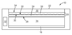
도 1은 예시적인 백라이트 디스플레이 장치(10)를 나타낸 개념도이다. 백라이트 디스플레이 장치(10)는 광원(12), 도광체(14), 반사체(16), LCD(18), 및 광학 스택(20)을 포함한다. 도시된 바와 같이, 광학 스택은 광 지향 필름(24) 및 광 지향 필름(24) 상에 배치된 비대칭 광 확산체(26)를 포함한다. 단일 광원(14)이 도광체(14)의 하나의 모서리에 인접한 백라이트 디스플레이 장치(10)가 예시되어 있지만, 다른 구성도 고려된다. 예를 들어, 백라이트 디스플레이 장치(10)는 도광체(14)의 하나 이상의 표면에 인접한 하나 초과의 광원(12)을 포함할 수 있다.
광원(14)은 형광 램프 또는 발광 다이오드(LED)와 같은 임의의 적합한 유형의 광원일 수 있다. 또한, 광원(14)은 복수의 개별 LED들과 같은 복수의 개별 광원들을 포함할 수 있다. LCD(18)의 외측 디스플레이 표면(22)을 조명하기 위해, 광원(12)으로부터의 광은 도광체(14)를 통해 일반적인 z-방향으로 전파된다. 광의 적어도 일부분은 도광체(14)의 상측 표면을 통해 빠져나가서 광학 스택(20) 내로 들어간다. 반사체(16)는 도광체(14)의 아래에 위치해 있고, 광을 광학 필름(20) 쪽으로 다시 반사시킨다.
백라이트 디스플레이 장치(10)의 도광체(14)는 당업계에 알려진 임의의 적합한 도광체일 수 있고, 1999년 12월 14일자의 미국 특허 제6,002,829호(윈스턴(Winston) 등) 및 2010년 11월 16일자의 제7,833,621호(존스(Jones) 등)에 기술되어 있는 예시적인 도광체들 중 하나 이상을 포함할 수 있다. 이들 미국 특허 각각의 전체 내용은 본 명세서에 참조로 포함된다. 도광체(14)에 인접한 반사체(16)에 적합한 재료는 향상된 경면 반사체(Enhanced Specular Reflector)(미국 미네소타주 세인트 폴 소재의 쓰리엠(3M)으로부터 구매가능함) 또는 백색 PET계 반사체를 포함할 수 있다.
광 지향 필름(24)은 제2 주 표면(28)의 반대쪽에 있는 구조화된 주 표면(30)을 포함한다. 구조화된 주 표면(30)(도 1에 도시되지 않은 구조물)은 제1 방향을 따라 연장되는 복수의 선형 구조물들을 포함할 수 있다. 도광체(14)로부터 광 지향 필름(24)으로 들어간 광의 일부분은 비대칭 광 확산체(26)로 들어가기 전에 광 지향 필름(24)에 의해 방향전환될 수 있는 한편, 광의 다른 부분들은 방향전환되지 않을 수 있거나 광학 스택(20)에 의해 방향전환되어 다시 도광체(14) 내로 들어갈 수 있다. 광이 반사체(16)에 의해 반사되어 다시 도광체(14) 내로 들어갈 수 있다는 의미에서 이 광의 일부는 "재순환"될 수 있다. 하기에 기술되는 바와 같이, 일부 실시예들에서, 광 지향 필름(24)은 평균 유효 투과율이 1.3 이상일 수 있다.
일부 실시예들에서, 광 지향 필름(24)의 제2 주 표면(28)은 광 확산성일 수 있다. 일부 실시예들에서, 제2 주 표면(28)은 또한, 예를 들어 기판 상에 침착된 불균일한 코팅에 의해 한정된 구조화된 표면일 수 있다. 광 지향 필름(24)에서는 구조화된 표면(30)으로서 상부 표면이 도시되어 있지만, 다른 실시예들에서는, 구조화된 표면(30)이 광 지향 필름(24)의 하부 표면일 수 있으며, 상부 표면은 제2 표면(28)일 수 있다.
광학 스택(20)은 또한 광 지향 필름(24) 상에 배치된 비대칭 광 확산체(26)를 포함한다. 비대칭 광 확산체(26)는 상부 주 표면(34) 및 광 지향 필름(24)의 구조화된 표면(30)에 인접한 하부 주 표면(32)을 포함한다. 광 지향 층(24)으로부터 비대칭 광 확산체(26)로 들어간 광은, 비대칭 확산체(26)를 빠져나가서 디스플레이(18) 내로 들어가서 디스플레이 표면(22)을 조명하기 전에 하나 이상의 방향으로 확산되거나 퍼져 나갈 수 있다. 비대칭 광 확산체(26)는 광 확산체(26)로 들어간 광이 모든 방향으로 동일하게 확산되지 않고 대신에 광이 다른 방향보다 한 방향으로 더 많이 확산될 수 있다는 의미에서 "비대칭" 광 확산체로 지칭될 수 있다. 도 2에 관하여 하기에 기술되는 바와 같이, 비대칭 광 확산체(26)는 제3 방향(d3)보다 제2 방향(d2)으로 더 확산성이 되도록 구성될 수 있다. 비대칭 확산체(26)는, 예를 들어 광 지향 층(24)으로 인한 원치 않는 시각적 아티팩트의 분해능(resolution)을 감소시키도록 구성될 수 있다.
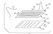
도 2는 광 지향 필름(24) 및 비대칭 광 확산체(26)를 포함하는 광학 스택(20)의 분해도를 예시하는 개념도이다. 구조화된 주 표면(30)은 비대칭 확산체(26)와 대면하고, 제2 주 표면(28)은 비대칭 확산체(26)로부터 멀어지는 쪽으로 대면한다. 구조화된 주 표면(30)은 제1 방향(d1)을 따라 연장되는 복수의 선형 구조물들 - 개별적으로 표시된 선형 구조물(31)을 포함함 - 을 포함하며, 이들은 LCD(18)를 향하여 광 지향 필름(24)으로 들어간 광의 적어도 일부분을 (예를 들어, 축방향 쪽으로) 방향전환시키는 역할을 할 수 있다. 설명의 용이함을 위하여, 복수의 선형 구조물들의 특성은 개별 선형 구조물(31)을 참조하여 일반적으로 기술되어 있지만, 이러한 특성은 구조화된 주 표면(30)의 모든 복수의 선형 구조물들에 일반적으로 적용된다.
일부 실시예들에서, 선형 구조물(31)은 제1 방향(d1)을 따라 연장되는 프리즘의 형태를 취할 수 있다. 그러한 예에서, 광 지향 필름(24)은 프리즘형 필름으로 지칭될 수 있다. 이들 프리즘은 광 지향 필름(24)의 표면으로부터 돌출될 수 있으며, 피크에서 만나서 피크각을 형성하는 2개 이상의 소면(facet)을 포함할 수 있다. 일부 실시예들에서, 선형 구조물(31)은 70 내지 120도, 예컨대 80 내지 110도 또는 85 내지 95도의 범위로 피크각을 형성하는 소면들을 포함하는 프리즘을 포함할 수 있지만, 다른 피크각들도 고려된다. 일부 실시예들에서, 적합한 광 지향 필름은 (미국 미네소타주 세인트 폴 소재의 쓰리엠으로부터 구매가능한) 휘도 향상 필름(Brightness Enhancing Film) 또는 "BEF"를 포함할 수 있다. 선형 구조물(31)이 프리즘에 관하여 기술되어 있지만, 다른 구조물들도 고려된다. 일부 실시예들에서, 선형 구조물(31)은 원통형 단면 프로파일을 가질 수 있거나 또는 그 프로파일 내에 선형 및 곡선형 특징부의 조합을 가질 수 있다. 선형 구조물(31)은 방향(d1)을 따라 높이, 기울기(tilt) 및 단면에서 변동을 나타낸다.
상기 기재된 바와 같이, 제2 표면(28)은 광 확산성일 수 있다. 예를 들어, 제2 표면(28)은 무광택 코팅을 포함할 수 있다. 일부 실시예들에서, 제2 표면(28)은 구조화된 표면일 수 있다. 예를 들어, 제2 표면(28)은 불균일한 표면 구조물을 제공하는 불균일한 코팅에 의해 한정될 수 있다. 또한, 일부 실시예들에서, 제2 표면(28)은 구조화된 주 표면(30)보다 비대칭 광 확산체(26)에 더 가까이 있을 수 있다(즉, 제2 표면(28)은 비대칭 광 확산체(26)와 대면할 수 있음).
광 지향 필름(24)이 액정 디스플레이 시스템에서 사용되는 경우, 광 지향 필름(24)은 디스플레이의 축상 휘도를 증가시키거나 개선시킬 수 있다. 그러한 경우에, 광 지향 필름은 1 초과의 유효 투과율 또는 상대 이득을 갖는다. 전술된 바와 같이, 일부 실시예들에서, 광학 스택(20)의 광 지향 필름(24)은 평균 유효 투과율이 1.3 이상, 예컨대 1.4 이상, 1.5 이상, 1.6 이상, 또는 1.7 이상일 수 있다.
본 명세서에서 사용되는 바와 같이, "유효 투과율"은 이 필름이 디스플레이 시스템 내 정위치에 있는 디스플레이 시스템의 축상 휘도 대 이 필름이 정위치에 있지 않은 디스플레이의 축상 휘도의 비이다. 유효 투과율(ET)은 개략 측면도가 도 5에 도시되어 있는 광학 시스템(200)을 사용하여 측정될 수 있다. 광학 시스템(200)은 광학 축(250) 상에 중심이 설정되며, 방출 또는 출사 표면(212)을 통해 램버시안 광(lambertian light)(215)을 방출하는 중공형 램버시안 광 박스, 선형 광 흡수 편광기(220), 및 광 검출기(230)를 포함한다. 광 박스(210)는 광섬유(270)를 통해 광 박스의 내부(280)에 연결된 안정화된 광대역 광원(260)에 의해 조명된다. 이 광학 시스템에 의해 ET를 측정하려는 시험 샘플이 광 박스와 흡수 선형 편광기 사이의 위치(240)에 배치된다.
선형 프리즘(150)이 광 검출기와 대면하고 미세구조물(160)이 광 박스와 대면한 상태에서 광 지향 필름을 위치(240)에 배치함으로써 광 지향 필름(24)의 ET가 측정될 수 있다. 다음에, 스펙트럼 가중된(spectrally weighted) 축상 휘도 I1(광학 축(250)을 따른 휘도)이 선형 흡수 편광기를 통해 광 검출기에 의해 측정된다. 다음에, 광 지향 필름이 제거되고 스펙트럼 가중된 휘도 I2가 광 지향 필름을 위치(240)에 배치하지 않은 상태로 측정된다. ET는 비 I1/I2이다. ET0은 선형 프리즘(150)이 선형 흡수 편광기(220)의 편광축에 평행인 방향을 따라 연장될 때의 유효 투과율이고, ET90은 선형 프리즘(150)이 선형 흡수 편광기의 편광축에 수직인 방향을 따라 연장될 때의 유효 투과율이다. 평균 유효 투과율(ETA)은 ET0과 ET90의 평균이다.
임의의 적합한 재료가 광 지향 필름(24)을 형성하는 데 사용될 수 있다. 전술된 바와 같이, 복수의 테이퍼진 돌출부들(30)의 형상 및 재료는 광 지향 층(26)을 통과하는 도광체(14)로부터의 광의 적어도 일부분이 입사광의 발산을 감소시키고 제1 방향을 따라 전파하는 입사광의 대부분을 제1 방향과 상이한 제2 방향으로 방향전환시킬 수 있게 할 수 있다. 적합한 재료는 광학 중합체, 예컨대 아크릴레이트, 폴리카르보네이트, 폴리스티렌, 스티렌 아크릴로 니트릴 등을 포함할 수 있다. 적합한 재료는 (미국 미네소타주 세인트 폴 소재의 쓰리엠으로부터 구매가능한) 휘도 향상 필름 또는 "BEF"를 형성하는 데 사용되는 재료들을 포함할 수 있다. 일부 실시예들에서, 광 지향 필름(24)을 형성하는 데 사용되는 재료는 굴절률이 대략 1.4 내지 대략 1.7, 예컨대 대략 1.45 내지 대략 1.6일 수 있다.
광 지향 필름(24)은 기판 두께 및 기판 표면 위로의 프리즘 높이에 의해 한정된 전체 두께를 포함할 수 있다. 일부 실시예들에서, 광 지향 필름(24)은 기판 두께가 약 25 마이크로미터 내지 약 250 마이크로미터이고, 프리즘 높이가 약 8 마이크로미터 내지 약 50 마이크로미터일 수 있다. 일부 실시예들에서, 광 지향 필름(24)의 전체 두께는 약 30 마이크로미터 내지 약 300 마이크로미터일 수 있다. 다른 두께 및 높이도 고려된다.
도 2에 예시된 바와 같이, 비대칭 광 확산체(26)는 광 지향 필름(24) 상에 배치되고, 하부 표면(32) 및 상부 표면(34)을 포함한다. 일반적으로, 비대칭 광 확산체(26)는 다른 방향보다 한 방향으로 더 많이 광을 확산시킬 수 있다. 도 2에 예시된 바와 같이, 비대칭 광 확산체(26)는 제2 방향(d2)과 직교하는 제3 방향(d3)을 따르는 것보다 제2 방향(d2)을 따라 더 확산성일 수 있다. 제3 방향(d3)을 따르는 것에 대한 제2 방향(d2)을 따르는 비대칭 광 확산체(26)의 상대 확산성을 예시하기 위하여, 제1 시야각(A1)을 갖는 제2 방향(d2)으로의 확산이 제2 시야각(A2)을 갖는 제3 방향으로의 확산에 대하여 도시되어 있다. 도시된 바와 같이, A2는 비대칭 광 확산체(26)가 제3 방향(d3)을 따르는 것보다 제2 방향(d2)을 따라 광을 더 많이 산란시킬 수 있다는 것을 나타내는데, 예를 들어 방향(d2)을 따르는 곡선의 폭이 방향(d3)을 따르는 곡선의 폭보다 더 크기 때문이다.
일부 실시예들에서, 비대칭 광 확산체(26)는 제1 시야각(A1)으로 제2 방향(d2)을 따라, 그리고 제2 시야각(A2)으로 제3 방향(d3)을 따라 광을 산란시키며, 이때 A1/A2는 1.5 이상, 예컨대 2 이상, 2.5 이상, 3 이상, 4 이상, 6 이상, 8 이상, 또는 10 이상이다. 본 명세서에서 사용되는 바와 같이, 시야각은 휘도가 최대값의 1/2인 각도를 지칭할 수 있다.
도 2에 도시된 바와 같이, 제1 광 지향 필름(24)은 제2 방향(d2)이 제1 방향(d1)과 각도를 형성하도록 비대칭 광 확산체(26)에 대해 배치될 수 있다. 일부 실시예들에서, 제1 광 지향 필름(24)은 제2 방향(d2)이 제1 방향(d1)과 이루는 각도가 0 초과(즉, d2와 d1이 평행하지 않음) 및 60도 미만, 예컨대 0 초과 50도 미만 또는 0 초과 40도 미만이도록 비대칭 광 확산체(26)에 대해 배치될 수 있다. 상기에 언급된 바와 같이, 본 명세서에 기술된 광학 스택들의 일부 실시예들은 디스플레이 장치에서의 결함, 예컨대 광 지향 필름(24)과 관련된 색 불균일성 및 무아레를 실질적으로 제거할 수 있는 한편, 추가로 확산 필름의 사용과 관련된 스파클을 최소화할 수 있다는 것으로 판단되었다.
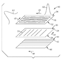
도 3은 다른 광학 필름 스택(40)의 분해도를 예시하는 개념도이다. 광학 필름 스택(40)은 제1 광 지향 필름(24) 및 비대칭 광 확산체(26)를 포함하며, 광학 필름 스택(20)과 실질적으로 동일할 수 있다. 그러나, 광학 필름 스택(40)은 제1 광 지향 필름(24) 상에 배치된 제2 광 지향 필름(42)을 포함한다. 제1 광 지향 필름(24)은 비대칭 광 확산체(26)로부터 제2 광 지향 필름(42)을 분리한다. 제2 광 지향 필름(42)은 제2 주 표면(46)의 반대쪽에 있는 제2 구조화된 표면(44)을 포함한다. 구조화된 주 표면(44)은 비대칭 확산체(26)와 대면하고, 제2 주 표면(46)은 비대칭 확산체(26)로부터 멀어지는 쪽으로 대면한다.
제2 광 지향 필름(42)은 제1 광 지향 필름(24)에 관하여 본 명세서에 기술된 것과 동일하거나 실질적으로 유사한 특성을 가질 수 있다. 예를 들어, 광학 스택(40)의 제2 광 지향 필름(42)은 평균 유효 투과율이 1.3 이상, 예컨대 1.4 이상, 1.5 이상, 1.6 이상, 또는 1.7 이상일 수 있다. 다른 예로서, 제2 표면(46)은 광 확산성일 수 있다. 예를 들어, 제2 표면(46)은 무광택 코팅을 포함할 수 있다. 일부 실시예들에서, 제2 표면(46)은 구조화된 표면일 수 있다. 예를 들어, 제2 표면(46)은 불균일한 표면 구조물을 제공하는 불균일한 코팅에 의해 한정될 수 있다. 또한, 일부 실시예들에서, 제2 표면(46)은 구조화된 주 표면(44)보다 비대칭 광 확산체(26)에 더 가까이 있을 수 있다(즉, 제2 표면(46)은 비대칭 광 확산체(26)와 대면할 수 있음). 일부 실시예들에서, 단일 프리즘 필름이 그러한 방식으로 터닝 필름(turning film)으로서 반전되는 것이 가능할 수 있지만, 그러한 반전된 필름이 반전 또는 반전되지 않는 다른 구조물 필름을 동반하지 않을 수 있다.
다른 예로서, 제1 광 지향 필름(24)과 유사하게, 제2 광 지향 필름(42)은 복수의 선형 구조물들(예를 들어, 70 내지 120도, 예컨대 80 내지 110도 또는 85 내지 95도의 범위로 피크각을 형성하는 소면들로 한정되는 복수의 선형 프리즘들)을 포함한다. 그러나, 제2 광 지향 필름(40)은 제1 광 지향 필름(40)에 대해 배향되기 때문에, 구조화된 표면(44)의 복수의 선형 구조물들은 제1 방향(d1)보다는 오히려 제4 방향(d4)을 따라 연장된다. 일부 실시예들에서, 광학 스택(40)은 제2 방향(d2)이 제4 방향(d4)보다는 제1 방향(d1)과 더 작은 각도를 형성하도록 배향될 수 있다. 도 3에 도시된 바와 같이, 제4 방향(d4)은 제1 방향과 실질적으로 직교한다. 일부 경우에, 제1 및 제2 광 지향 필름(24, 42)은 교차된 배향인 것으로 언급될 수 있다.
광학 스택(20) 또는 광학 스택(40) 중 어느 것에서도, 비대칭 광 확산체(26)는 본 명세서에 기술된 특성을 제공할 수 있는 임의의 적합한 비대칭 광 확산체일 수 있다. 일부 실시예들에서, 비대칭 광 확산체(26)는 체적형 (또는 벌크형) 확산체(volume (or bulk) diffuser)를 포함할 수 있다. 일부 실시예들에서, 체적형 확산체는 제2 굴절률을 갖는 입자들이 퍼져 있는 제1 굴절률을 갖는 호스트 재료를 포함할 수 있는데, 여기서 제1 및 제2 굴절률은 0.01 이상 상이하며, 입자들의 체적 분율은 0.1% 이상이다. 그러한 실시예들에서는, 입자들에 의해 반사 및 굴절이 반복되고, 그럼으로써 원래의 광선 방향을 변경시킴으로 광 확산이 달성된다. 일부 실시예들에서, 비대칭 광 확산체(26)는 구조화된 주 표면을 포함하는 표면 확산체를 포함할 수 있다. 예를 들어, 비대칭 광 확산체(26)는 미세복제된 무광택 코팅을 포함할 수 있다. 일부 실시예들에서, 적합한 비대칭 광 확산체는, 출원 번호가 PCT/US2010/036018호이고 2010년 5월 25일자로 출원된 공개된 PCT 특허 출원 WO 2010/141261호에 기술된 예들 중 하나 이상을 포함할 수 있으며, 이의 전체 내용은 본 명세서에 참조로 포함된다.
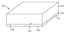
일 실시예에서, 도 6에 도시된 바와 같이, 비대칭 광 확산체(26)는 기판(170) 상에 침착된 무광택 층(140)을 포함할 수 있다. 기판(170)은 PET, 폴리카르보네이트, 또는 다른 적합한 재료를 포함할 수 있다. 무광택 층(140) 내의 미세구조물(160)은, 광을 방향전환시키고 휘도를 향상시키는 광 지향 필름의 기능에 대한 역효과가 전혀 또는 거의 없이, 바람직하지 않은 물리적 결함(예컨대, 스크래치) 및/또는 광학 결함(예컨대, 디스플레이 또는 조명 시스템에서의 조명으로부터의 바람직하지 않게 밝은 또는 "핫" 스폿)을 감추도록 설계될 수 있다.
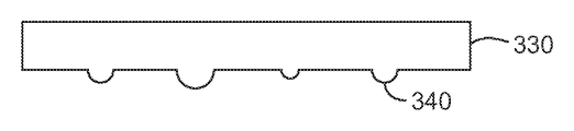
미세구조물(160)은 응용에 바람직할 수 있는 임의의 유형의 미세구조물일 수 있다. 일부 경우에, 미세구조물(160)은 함몰부일 수 있다. 예를 들어, 도 7a는 무광택 층(140)과 유사하고 함몰된 미세구조물(320)을 포함하는 무광택 층(310)의 개략 측면도이다. 일부 경우에, 미세구조물(160)은 돌출부일 수 있다. 예를 들어, 도 7b는 무광택 층(140)과 유사하고 돌출한 미세구조물(340)을 포함하는 무광택 층(330)의 개략 측면도이다.
일부 경우에, 미세구조물(160)은 규칙적인 패턴을 형성한다. 예를 들어, 도 8a는 미세구조물(160)과 유사하고 주 표면(415)에 규칙적인 패턴을 형성하는 미세구조물(410)의 개략 평면도이다. 일부 경우에, 미세구조물(160)은 불규칙적인 패턴을 형성한다. 예를 들어, 도 8b는 미세구조물(160)과 유사하고 불규칙적인 패턴을 형성하는 미세구조물(420)의 개략 평면도이다. 일부 경우에, 미세구조물(160)은, 예를 들어 표면 지형의 2차원 푸리에 스펙트럼에서 하나 이상의 피크들의 존재에 의해 입증되는 바와 같이, 랜덤한 것처럼 보이지만 반복 패턴 양상을 갖는 유사-랜덤(pseudo-random) 패턴을 형성한다.
일반적으로, 비대칭 확산체(26)의 미세구조물(160)은 임의의 높이 및 임의의 높이 분포를 가질 수 있다. 일부 경우에, 미세구조물(160)의 평균 높이(즉, 평균 피크 높이 - 평균 밸리 높이)는 약 5 마이크로미터 이하, 또는 약 4 마이크로미터 이하, 또는 약 3 마이크로미터 이하, 또는 약 2 마이크로미터 이하, 또는 1 마이크로미터 이하, 또는 약 0.9 마이크로미터 이하, 또는 약 0.8 마이크로미터 이하, 또는 약 0.7 마이크로미터 이하이다.
도 9는 비대칭 확산체(26)의 무광택 층(140)의 일부분의 개략 측면도이다. 특히, 도 9는 주 표면(32) 및 대면하는 주 표면(142)으로 미세구조물(160)을 도시하고 있다. 미세구조물(160)은 미세구조물의 표면을 가로질러 기울기 분포를 갖는다. 예를 들어, 미세구조물은 위치(510)에서 기울기 θ를 갖는데, 여기서 θ는 위치(510)에서 미세구조물 표면에 수직인(α=90 도인) 법선(520)과 동일한 위치에서 미세구조물 표면에 접하는 접선(530) 사이의 각도이다. 기울기 θ는 또한 접선(530)과 무광택 층의 주 표면(142) 사이의 각도이다.
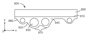
도 10은 기판(170)과 유사한 기판(850) 상에 배치된 무광택 층(860)을 포함하는 비대칭 광 확산체(800)의 개략 측면도이다. 무광택 층(860)은 기판(850)에 부착된 제1 주 표면(810), 제1 주 표면의 반대쪽에 있는 제2 주 표면(820), 및 결합제(840) 중에 분산된 복수의 입자들(830)을 포함한다. 제2 주 표면(820)은 복수의 미세구조물들(870)을 포함한다. 미세구조물들(870)의 상당 부분, 예컨대 약 50% 이상, 또는 약 60% 이상, 또는 약 70% 이상, 또는 약 80% 이상, 또는 약 90% 이상이 입자들(830) 상에 배치되고 입자들(830)로 인해 주로 형성된다. 다시 말하면, 입자들(830)은 미세구조물들(870)의 형성의 주 원인이다. 그러한 경우에, 입자들(830)은 약 0.25 마이크로미터 초과, 또는 약 0.5 마이크로미터 초과, 또는 약 0.75 마이크로미터 초과, 또는 약 1 마이크로미터 초과, 또는 약 1.25 마이크로미터 초과, 또는 1.5 마이크로미터 초과, 또는 약 1.75 마이크로미터 초과, 또는 약 2 마이크로미터 초과인 평균 크기를 가진다.
일부 경우에, 무광택 층(140)은 무광택 층(860)과 유사할 수 있고, 제2 주 표면(32) 내의 미세구조물(160)의 형성의 주 원인인 복수의 입자들을 포함할 수 있다.
입자들(830)은 응용에 바람직할 수 있는 임의의 유형의 입자일 수 있다. 예를 들어, 입자들(830)은 폴리메틸 메타크릴레이트(PMMA), 폴리스티렌(PS), 또는 응용에 바람직할 수 있는 임의의 다른 재료로 제조될 수 있다. 일반적으로, 입자들(830)의 굴절률은 결합제(840)의 굴절률과 상이하지만, 일부 경우에 이들은 동일한 굴절률을 가질 수 있다. 예를 들어, 입자들(830)은 약 1.35, 또는 약 1.48, 또는 약 1.49, 또는 약 1.50의 굴절률을 가질 수 있고, 결합제(840)는 약 1.48, 또는 약 1.49, 또는 약 1.50의 굴절률을 가질 수 있다.
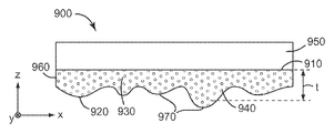
일부 경우에, 무광택 층(140)은 입자들을 포함하지 않는다. 일부 경우에, 무광택 층(140)은 입자들을 포함하지만, 이들 입자가 미세구조물(160)의 형성의 주 원인은 아니다. 예를 들어, 도 11은 기판(170)과 유사한 기판(950) 상에 배치된 무광택 층(140)과 유사한 무광택 층(960)을 포함하는 비대칭 광 확산체(900)의 개략 측면도이다. 무광택 층(960)은 기판(950)에 부착된 제1 주 표면(910), 제1 주 표면의 반대쪽에 있는 제2 주 표면(920), 및 결합제(940) 중에 분산된 복수의 입자들(930)을 포함한다. 제2 주 표면(970)은 복수의 미세구조물들(970)을 포함한다. 비록 무광택 층(960)이 입자들(930)을 포함하지만, 이들 입자는 미세구조물들(970)의 형성의 주 원인은 아니다. 예를 들어, 일부 경우에, 입자들은 미세구조물들의 평균 크기보다 훨씬 더 작다. 그러한 경우에, 이들 미세구조물은, 예를 들어 구조화된 툴을 미세복제함으로써 형성될 수 있다. 그러한 경우에, 입자들(930)의 평균 크기는 약 0.5 마이크로미터 미만, 또는 약 0.4 마이크로미터 미만, 또는 약 0.3 마이크로미터 미만, 또는 약 0.2 마이크로미터 미만, 또는 약 0.1 마이크로미터 미만이다. 그러한 경우에, 미세구조물들(970)의 상당 부분, 예컨대 약 50% 이상, 또는 약 60% 이상, 또는 약 70% 이상, 또는 약 80% 이상, 또는 약 90% 이상이 약 0.5 마이크로미터 초과, 또는 약 0.75 마이크로미터 초과, 또는 약 1 마이크로미터 초과, 또는 약 1.25 마이크로미터 초과, 또는 약 1.5 마이크로미터 초과, 또는 약 1.75 마이크로미터 초과, 또는 약 2 마이크로미터 초과인 평균 크기를 갖는 입자들 상에 배치되지 않는다. 일부 경우에, 입자들(930)의 평균 크기는 미세구조물들(930)의 평균 크기보다 약 2배 이상, 또는 약 3배 이상, 또는 약 4배 이상, 또는 약 5배 이상, 또는 약 6배 이상, 또는 약 7배 이상, 또는 약 8배 이상, 또는 약 9배 이상, 또는 약 10배 이상만큼 더 작다. 일부 경우에, 무광택 층(960)이 입자들(930)을 포함하는 경우, 무광택 층(960)은 이들 입자의 평균 크기보다 약 0.5 마이크로미터 이상, 또는 약 1 마이크로미터 이상, 또는 약 1.5 마이크로미터 이상, 또는 약 2 마이크로미터 이상, 또는 약 2.5 마이크로미터 이상, 또는 약 3 마이크로미터 이상만큼 더 큰 평균 두께 "t"를 갖는다. 일부 경우에, 무광택 층이 복수의 입자들을 포함하는 경우, 무광택 층의 평균 두께는 이들 입자의 평균 두께보다 약 2배 이상, 또는 약 3배 이상, 또는 약 4배 이상, 또는 약 5배 이상, 또는 약 6배 이상, 또는 약 7배 이상, 또는 약 8배 이상, 또는 약 9배 이상, 또는 약 10배 이상만큼 더 크다.
비대칭 확산체 층(26)은 응용에 바람직할 수 있는 임의의 제작 방법을 사용하여 제조될 수 있다. 예를 들어, 비대칭 확산체 층(26)이 툴로부터 미세복제를 통해 형성되는 경우에, 이러한 툴은 인그레이빙(engraving) 또는 다이아몬드 터닝(diamond turning)을 사용하는 것과 같은 임의의 이용가능한 제작 방법을 사용하여 제작될 수 있다. 예시적인 다이아몬드 터닝 시스템 및 방법은, 예를 들어 PCT 공개 출원 WO 00/48037호, 및 미국 특허 제7,350,442호 및 제7,328,638호에 기술된 바와 같은 고속 툴 서보(fast tool servo, FTS)를 포함하고 이용할 수 있으며, 이들의 개시 내용은 전체적으로 본 명세서에 참조로 포함된다. 비대칭 확산체(26)를 형성하기 위한 다른 적합한 기술이 또한 고려된다.
도 4는 본 명세서에 기술된 광학 스택들 중 하나 이상에 사용될 수 있는 예시적인 비대칭 광 확산체(48)의 사진이다. 전술된 바와 같이, 비대칭 광 확산체(48)는 복수의 세장형 구조물들(도 4에는 표시되지 않음)을 포함할 수 있다. 일부 실시예들에서, 그러한 세장형 구조물들의 평균 길이, 폭, 및 높이는 이들 구조물이 단부에서 단부까지 신장 방향을 따라 테이퍼지고 중심에서 불룩해지도록 하는 것들일 수 있다. 일부 실시예들에서, 그러한 구조물들은 신장 방향을 따르는 것보다 신장 방향에 수직한 방향으로 광을 더 많이 확산시킨다.
도 12는 비대칭 확산체(26)의 미세구조물(160) 및 무광택 층(140)을 생성하도록 미세복제될 수 있는 툴을 절삭하는 데 사용될 수 있는 절삭 툴 시스템(1000)의 개략 측면도이다. 절삭 툴 시스템(1000)은 스레드 컷(thread cut) 선삭 공정을 사용하고, 구동기(1030)에 의해 중심축(1020) 주위를 회전하고/하거나 이를 따라 이동할 수 있는 롤(1010), 및 롤 재료를 절삭하기 위한 커터(1040)를 포함한다. 커터는 서보(1050) 상에 장착되고, 구동기(1060)에 의해 롤 내로 이동되고/되거나 x-방향을 따라 롤을 따라 이동될 수 있다. 일반적으로, 커터(1040)는 롤 및 중심축(1020)에 수직으로 장착되고, 롤이 중심축 주위로 회전하는 동안 롤(1010)의 인그레이빙 가능한 재료 내로 구동된다. 이어서, 커터는 중심축에 평행하게 구동되어 스레드 컷을 생성한다. 커터(1040)는 미세복제될 때 미세구조물(160)을 형성하는 특징부들을 롤 내에 생성하도록 높은 빈도 및 낮은 변위로 동시에 작동될 수 있다.
서보(1050)는 고속 툴 서보(FTS)이며, 커터(1040)의 위치를 신속하게 조정하는, 종종 PZT 스택으로 지칭되는 고상 압전 장치(solid state piezoelectric(PZT) device)를 포함한다. FTS(1050)는 x-방향, y-방향 및/또는 z-방향, 또는 축외(off-axis) 방향으로의 커터(1040)의 매우 정밀하면서도 고속의 이동을 가능하게 한다. 서보(1050)는 휴지 위치(rest position)에 대한 제어된 이동을 발생시킬 수 있는 임의의 고품질 변위 서보일 수 있다. 일부 경우에, 서보(1050)는 약 0.1 마이크로미터 또는 더 우수한 분해능으로 0 내지 약 20 마이크로미터 범위 내의 변위를 확실하게 그리고 반복가능하게 제공할 수 있다.
구동기(1060)는 중심축(1020)에 평행한 x-방향을 따라 커터(1040)를 이동시킬 수 있다. 일부 경우에, 구동기(1060)의 변위 분해능은 약 0.1 마이크로미터보다 우수하거나, 약 0.01 마이크로미터보다 우수하다. 미세구조물(160)의 최종 형상을 정확하게 제어하기 위하여 구동기(1030)에 의해 발생되는 회전 운동은 구동기(1060)에 의해 발생되는 병진 운동과 동기화된다.
롤(1010)의 인그레이빙 가능한 재료는 커터(1040)에 의해 인그레이빙될 수 있는 임의의 재료일 수 있다. 예시적인 롤 재료는 구리와 같은 금속, 다양한 중합체, 및 다양한 유리 재료를 포함한다.
커터(1040)는 임의의 유형의 커터일 수 있으며, 응용에 바람직할 수 있는 임의의 형상을 가질 수 있다. 예를 들어, 커터(1040)는 아크형 절삭 팁을 한정할 수 있다. 다른 예로서, 커터(1040)는 V형 절삭 팁(1125)을 한정할 수 있다. 또 다른 예로서, 커터(1040)는 구분적 선형(piece-wise linear) 절삭 팁 또는 곡선형 절삭 팁을 가질 수 있다.
본 발명의 다양한 실시 형태들을 설명하였다. 이들 및 다른 실시 형태들은 하기의 특허청구범위의 범주 내에 속한다.
예시적인 실시 형태는 하기의 것들을 포함한다:
항목 1. 제1 방향을 따라 연장되는 복수의 선형 구조물들을 포함하고 제2 주 표면의 반대쪽에 있는 구조화된 주 표면을 포함하고, 평균 유효 투과율이 1.3 이상인 제1 광 지향 필름; 및
광 지향 필름 상에 배치되고 제2 방향을 따라 더 확산성이고 제2 방향과 직교하는 제3 방향을 따라 덜 확산성이며, 제2 방향이 제1 방향과 이루는 각도가 0 초과 및 60도 미만인 비대칭 광 확산체를 포함하는 광학 스택.
항목 2. 제1 광 지향 필름의 제2 주 표면이 광 확산성인 항목 1의 광학 스택.
항목 3. 제1 광 지향 필름의 제2 주 표면이 구조화된 항목 1의 광학 스택.
항목 4. 복수의 선형 구조물들이 제1 방향을 따라 연장되는 복수의 선형 프리즘형 구조물들을 포함하는 청구항 1의 광학 스택.
항목 5. 각각의 선형 프리즘형 구조물이 피크 및 피크각을 가지며, 상기 피크각은 70 내지 120도의 범위인 항목 1의 광학 스택.
항목 6. 각각의 선형 프리즘형 구조물이 피크 및 피크각을 가지며, 상기 피크각은 80 내지 110도의 범위인 항목 1의 광학 스택.
항목 7. 각각의 선형 프리즘형 구조물이 피크 및 피크각을 가지며, 상기 피크각은 85 내지 95도의 범위인 항목 1의 광학 스택.
항목 8. 광 지향 필름의 평균 유효 투과율이 1.4 이상인 항목 1의 광학 스택.
항목 9. 광 지향 필름의 평균 유효 투과율이 1.5 이상인 항목 1의 광학 스택.
항목 10. 광 지향 필름의 평균 유효 투과율이 1.6 이상인 항목 1의 광학 스택.
항목 11. 광 지향 필름의 평균 유효 투과율이 1.7 이상인 항목 1의 광학 스택.
항목 12. 제1 광 지향 필름의 구조화된 주 표면이 비대칭 광 확산체와 대면하고, 제1 광 지향 필름의 제2 주 표면이 비대칭 광 확산체로부터 멀어지는 쪽으로 대면하는 항목 1의 광학 스택.
항목 13. 비대칭 광 확산체가 제1 시야각(A1)으로 제2 방향을 따라, 그리고 제2 시야각(A2)으로 제3 방향을 따라 광을 산란시키며, A1/A2가 1.5 이상인 항목 1의 광학 스택.
항목 14. 비대칭 광 확산체가 제1 시야각(A1)으로 제2 방향을 따라, 그리고 제2 시야각(A2)으로 제3 방향을 따라 광을 산란시키며, A1/A2가 2 이상인 항목 1의 광학 스택.
항목 15. 비대칭 광 확산체가 제1 시야각(A1)으로 제2 방향을 따라, 그리고 제2 시야각(A2)으로 제3 방향을 따라 광을 산란시키며, A1/A2가 2.5 이상인 항목 1의 광학 스택.
항목 16. 비대칭 광 확산체가 제1 시야각(A1)으로 제2 방향을 따라, 그리고 제2 시야각(A2)으로 제3 방향을 따라 광을 산란시키며, A1/A2가 3 이상인 항목 1의 광학 스택.
항목 17. 비대칭 광 확산체가 제1 시야각(A1)으로 제2 방향을 따라, 그리고 제2 시야각(A2)으로 제3 방향을 따라 광을 산란시키며, A1/A2가 4 이상인 항목 1의 광학 스택.
항목 18. 비대칭 광 확산체가 제1 시야각(A1)으로 제2 방향을 따라, 그리고 제2 시야각(A2)으로 제3 방향을 따라 광을 산란시키며, A1/A2가 6 이상인 항목 1의 광학 스택.
항목 19. 비대칭 광 확산체가 제1 시야각(A1)으로 제2 방향을 따라, 그리고 제2 시야각(A2)으로 제3 방향을 따라 광을 산란시키며, A1/A2가 8 이상인 항목 1의 광학 스택.
항목 20. 비대칭 광 확산체가 제1 시야각(A1)으로 제2 방향을 따라, 그리고 제2 시야각(A2)으로 제3 방향을 따라 광을 산란시키며, A1/A2가 10 이상인 항목 1의 광학 스택.
항목 21. 비대칭 광 확산체가 체적형 확산체를 포함하는 항목 1의 광학 스택.
항목 22. 비대칭 광 확산체가 구조화된 주 표면을 포함하는 표면 확산체를 포함하는 항목 1의 광학 스택.
항목 23. 제2 방향이 제1 방향과 이루는 각도가 0 초과 및 50도 미만인 항목 1의 광학 스택.
항목 24. 제2 방향이 제1 방향과 이루는 각도가 0 초과 및 40도 미만인 항목 1의 광학 스택.
항목 25. 제1 광 지향 필름이 비대칭 광 확산체와 제2 주 표면의 반대쪽에 있는 구조화된 주 표면을 포함하는 제2 광 지향 필름 사이에 배치되며, 제2 광 지향 필름의 구조화된 주 표면은 제1 방향과 직교하는 제4 방향을 따라 연장되는 복수의 선형 구조물들을 포함하고, 상기 광 지향 필름은 평균 유효 투과율이 1.3 이상인 항목 1의 광학 스택.
항목 26. 광 지향 필름의 평균 유효 투과율이 1.4 이상인 항목 25의 광학 스택.
항목 27. 광 지향 필름의 평균 유효 투과율이 1.5 이상인 항목 25의 광학 스택.
항목 28. 광 지향 필름의 평균 유효 투과율이 1.6 이상인 항목 25의 광학 스택.
항목 29. 제2 광 지향 필름의 제2 주 표면이 광 확산성인 항목 25의 광학 스택.
항목 30. 제2 광 지향 필름의 제2 주 표면이 구조화된 항목 25의 광학 스택.
항목 31. 제2 방향이 제4 방향보다 제1 방향과 더 작은 각도를 이루는 항목 25의 광학 스택.≪ 1 >
1 is a conceptual view showing an exemplary backlight display device.
2,
2 is a conceptual diagram illustrating an exemplary optical film stack.
3,
3 is a conceptual diagram illustrating another exemplary optical film stack.
<Fig. 4>
4 is a photograph of an exemplary asymmetric light diffuser.
5,
5 is a conceptual diagram showing an exemplary optical system for measuring effective transmittance.
6,
6 is a conceptual diagram showing an exemplary asymmetric light diffuser.
7A and 7B,
7A and 7B are schematic side views of an exemplary matte layer.
8A and 8B,
8A and 8B are schematic plan views of exemplary microstructures of an exemplary asymmetric light diffuser.
9,
9 is a schematic side view of an exemplary matte layer.
<Fig. 10>
10 is a schematic side view of an exemplary asymmetric light diffuser.
11)
11 is a schematic side view of another exemplary asymmetric light diffuser.
12,
12 is a schematic side view of an exemplary cutting tool system.
DETAILED DESCRIPTION OF THE INVENTION [
In general, the present invention relates to an optical film stack that can be used, for example, in a backlight display device. The optical stack may include a light directing film having a structured major surface comprising a plurality of linear structures extending along a first direction. The optical stack may also include an asymmetric light diffuser disposed on the light directing film. The asymmetric light diffusers may be more diffusing along the second direction while less diffusing along the third direction orthogonal to the second direction. The asymmetric light diffuser may be disposed such that the angle formed by the second direction with respect to the first direction is greater than 0 and less than 60 degrees with respect to the light directing film.
In some embodiments, the backlight display device may include a light source, a light guide, a liquid crystal display (LCD), and an optical film stack between the light guide and the LCD. In such embodiments, the light emanating from the backlight may be used to illuminate the LCD after proceeding through the light guide and the optical film stack. More specifically, light escaping from the light guide can travel through the optical film stack before entering the LCD.
In some embodiments, the display device may include a back reflector layer that is separated from the stack of light management films by a light guide. The combination of the optical stack, the light guide, and the reflective layers may be referred to as a backlight stack. When the layers of the backlight stack are oriented substantially parallel to the display surface of the LCD and the light source is adjacent to one or more edges, the backlight stack includes a back reflector, a light guide, one or more light directing films, They can be included in that order. In some embodiments, the light directing film can be made of a transparent substrate on which a plurality of parallel linear prisms with a 90 degree apex angle are on top. In the case where the backlight stack includes two light directing layers, the prisms of the top surface prism film can be oriented such that they generally travel in a direction orthogonal to the prisms of the front surface prism film. In such a case, the prism films may be described as being in an intersecting orientation and may be configured to redirect a portion of the light from the light guide to the LCD.
In some embodiments, there may be one or more display defects associated with the use of such light directing film. For example, in some cases, the use of one or more light directing films can result in interference between linear prism structures, interference between such structures and their reflection, or a moiré pattern arising from both. In order to cope with such defects, a light-diffusing layer, for example a matte layer, can be used to spread light out of the light-directing layer before illuminating the display. However, the use of such a light diffusing layer can cause sparkle in the display. As used herein, the term sparkle refers to granularity that depends on the viewing angle of the display device.
According to some embodiments of the present invention, the optical stack may further include a second diffuser film that substantially eliminates color heterogeneity and moiré associated with defects in the first light directing film, e.g., a display device, e.g., a light directing film, And an asymmetric light diffuser disposed relative to the first light directing film in a manner that minimizes sparkle associated with the first light directing film. For example, the structured surface of the light directing film may comprise a plurality of linear structures (e.g., prisms) extending along the first direction, and the asymmetric light diffusing element may be further diffused along the second direction And may be less diffusing along a third direction orthogonal to the second direction. In such a case, the light directing film may be arranged such that the angle formed by the second direction with respect to the first direction is greater than 0 and less than 60 degrees with respect to the light diffusing body. As mentioned above, in some cases, such an optical film substantially minimizes sparkle associated with use of the diffusing film, while substantially eliminating color imperfections and moiré associated with defects in the display device, such as a light directing film . As will be further described below, in some embodiments, the optical stack may include one or more additional layers in addition to the layers of the first light directing film and the asymmetric light diffusing body.
Fig. 1 is a conceptual diagram showing an exemplary
The
The
The
In some embodiments, the second
The
2 is a conceptual diagram illustrating an exploded view of an
In some embodiments, the
As described above, the
When the
As used herein, "effective transmittance" is the ratio of the axial brightness of the display system in which this film is in place in the display system to the axial brightness of the display in which the film is not in position. The effective transmittance (ET) can be measured using the
The ET of the
Any suitable material may be used to form the
The
As illustrated in FIG. 2, the asymmetric
In some embodiments, the asymmetric
2, the first
3 is a conceptual diagram illustrating an exploded view of another
The second
As another example, similar to the first
In either the
In one embodiment, as shown in FIG. 6, the asymmetric
In some cases, the
In general, the
9 is a schematic side view of a portion of the
10 is a schematic side view of an asymmetric
The
The
In some cases, the
The
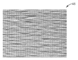
4 is a photograph of an exemplary asymmetric
12 is a schematic side view of a
The
The
The engraisable material of the
The
Various embodiments of the invention have been described. These and other embodiments are within the scope of the following claims.
Exemplary embodiments include the following:
Item 1. A first light directing film comprising a plurality of linear structures extending along a first direction and comprising a structured major surface opposite the second major surface and having an average effective transmittance of 1.3 or greater; And
The second direction being less diffusing along a third direction that is more diffusing along the second direction and orthogonal to the second direction and is disposed on the light directing film and having an angle greater than 0 and less than 60 degrees, An optical stack comprising an optical diffuser.
Item 3. The optical stack of item 1, wherein the second major surface of the first light directing film is structured.
Item 4. The optical stack of claim 1, wherein the plurality of linear structures comprises a plurality of linear prismatic structures extending along a first direction.
Item 5. The optical stack of item 1, wherein each linear prismatic structure has a peak and a peak angle, said peak angle being in the range of 70 to 120 degrees.
Item 6. The optical stack of item 1, wherein each linear prismatic structure has a peak and a peak angle, said peak angle being in the range of 80 to 110 degrees.
Item 7. The optical stack of item 1, wherein each linear prismatic structure has a peak and a peak angle, and the peak angle is in a range of 85 to 95 degrees.
Item 8. The optical stack of item 1, wherein the average effective transmittance of the light directing film is at least 1.4.
Item 9. The optical stack of item 1, wherein the average effective transmittance of the light directing film is at least 1.5.
Item 11. The optical stack of item 1, wherein the average effective transmittance of the light directing film is at least 1.7.
Item 13. Asymmetric light diffusing element has a first viewing angle A One ) Along a second direction, and a second viewing angle A 2 ) Scattering light along the third direction, and A One / A 2 Gt; 1.5 < / RTI >
Item 15. Asymmetric light diffusing element has a first viewing angle A One ) Along a second direction, and a second viewing angle A 2 ) Scattering light along the third direction, and A One / A 2 0.0 > 2.5 < / RTI >
Item 17. Asymmetric light diffusing element has a first viewing angle A One ) Along a second direction, and a second viewing angle A 2 ) Scattering light along the third direction, and A One / A 2 0.0 > 1 < / RTI >
Item 19. The asymmetric light diffuser has a first viewing angle A One ) Along a second direction, and a second viewing angle A 2 ) Scattering light along the third direction, and A One / A 2 Lt; RTI ID = 0.0 > 8 < / RTI >
Item 21. The optical stack of item 1, wherein the asymmetric light diffuser comprises a volumetric diffuser.
Item 23. The optical stack of item 1, wherein the angle of the second direction with the first direction is greater than 0 and less than 50 degrees.
Item 25. A method according to item 25, wherein a first light directing film is disposed between an asymmetric light diffuser and a second light directing film comprising a structured major surface opposite the second major surface, and the structured main surface of the second light directing film And a plurality of linear structures extending along a fourth direction orthogonal to the first direction, wherein the light directing film has an average effective transmittance of at least 1.3.
Item 27. The optical stack of item 25, wherein the average effective transmittance of the light directing film is at least 1.5.
Item 29. The optical stack of item 25, wherein the second major surface of the second light directing film is light diffusing.
Claims (10)
광 지향 필름 상에 배치되고 제2 방향을 따라 더 확산성이고 제2 방향과 직교하는 제3 방향을 따라 덜 확산성이며, 제2 방향이 제1 방향과 이루는 각도가 0 초과 및 60도 미만인 비대칭 광 확산체를 포함하는 광학 스택.A first light directing film comprising a plurality of linear structures extending along a first direction and comprising a structured major surface opposite the second major surface and having an average effective transmittance of 1.3 or greater; And
The second direction being less diffusing along a third direction that is more diffusing along the second direction and orthogonal to the second direction and is disposed on the light directing film and having an angle greater than 0 and less than 60 degrees, An optical stack comprising an optical diffuser.
Applications Claiming Priority (3)
| Application Number | Priority Date | Filing Date | Title |
|---|---|---|---|
| US201161578318P | 2011-12-21 | 2011-12-21 | |
| US61/578,318 | 2011-12-21 | ||
| PCT/US2012/070375 WO2013096324A1 (en) | 2011-12-21 | 2012-12-18 | Optical film stack |
Publications (1)
| Publication Number | Publication Date |
|---|---|
| KR20140103172A true KR20140103172A (en) | 2014-08-25 |
Family
ID=47472139
Family Applications (1)
| Application Number | Title | Priority Date | Filing Date |
|---|---|---|---|
| KR1020147019766A KR20140103172A (en) | 2011-12-21 | 2012-12-18 | Optical film stack |
Country Status (6)
| Country | Link |
|---|---|
| US (1) | US20140355125A1 (en) |
| JP (2) | JP6293057B2 (en) |
| KR (1) | KR20140103172A (en) |
| CN (1) | CN104136950B (en) |
| TW (1) | TWI595277B (en) |
| WO (1) | WO2013096324A1 (en) |
Families Citing this family (15)
| Publication number | Priority date | Publication date | Assignee | Title |
|---|---|---|---|---|
| US20140355125A1 (en) * | 2011-12-21 | 2014-12-04 | 3M Innovative Properties Company | Optical film stack |
| JP6834957B2 (en) * | 2015-07-10 | 2021-02-24 | 日本ゼオン株式会社 | Liquid crystal display device |
| CN108027461B (en) | 2015-09-15 | 2022-07-22 | 3M创新有限公司 | Low-flash matte coating and preparation method thereof |
| JP7056152B2 (en) * | 2015-12-17 | 2022-04-19 | 日本ゼオン株式会社 | Liquid crystal display device |
| WO2017139611A1 (en) * | 2016-02-10 | 2017-08-17 | 3M Innovative Properties Company | Unitary optical film assembly |
| KR20190019594A (en) * | 2017-08-18 | 2019-02-27 | 엘지이노텍 주식회사 | Semiconductor device package |
| US11784458B2 (en) * | 2017-08-18 | 2023-10-10 | Suzhou Lekin Semiconductor Co., Ltd. | Surface-emitting laser package |
| CN111954831B (en) * | 2018-03-07 | 2024-02-02 | 凸版印刷株式会社 | Optical film, optical barrier film, and backlight unit |
| CN111989598B (en) | 2018-04-17 | 2022-08-02 | 株式会社Lg化学 | Light diffusion barrier film |
| CN108828840A (en) * | 2018-07-25 | 2018-11-16 | 武汉华星光电技术有限公司 | A kind of backlight module and liquid crystal display device |
| TWI726251B (en) * | 2018-10-30 | 2021-05-01 | 友達光電股份有限公司 | Display module |
| CN114335382A (en) * | 2018-12-07 | 2022-04-12 | 京东方科技集团股份有限公司 | Display module and preparation method thereof |
| US11668977B2 (en) | 2018-12-14 | 2023-06-06 | 3M Innovative Properties Company | Liquid crystal display having a frontside light control film |
| CN116134265A (en) * | 2020-07-28 | 2023-05-16 | 日东电工株式会社 | Building construction |
| CN112018140A (en) * | 2020-08-14 | 2020-12-01 | 清华大学 | Miniature spectrum chip based on random shape unit |
Family Cites Families (20)
| Publication number | Priority date | Publication date | Assignee | Title |
|---|---|---|---|---|
| US6002829A (en) | 1992-03-23 | 1999-12-14 | Minnesota Mining And Manufacturing Company | Luminaire device |
| US6322236B1 (en) | 1999-02-09 | 2001-11-27 | 3M Innovative Properties Company | Optical film with defect-reducing surface and method for making same |
| JP4288834B2 (en) * | 2000-07-27 | 2009-07-01 | 三菱電機株式会社 | Backlight for liquid crystal display device and liquid crystal display device |
| US6909480B2 (en) * | 2000-10-19 | 2005-06-21 | Daicel Chemical Industries, Ltd. | Anisotropic scattering sheet and its use |
| JP4156222B2 (en) * | 2000-10-25 | 2008-09-24 | ダイセル化学工業株式会社 | Surface light source unit and transmissive display device using the same |
| US7738754B2 (en) * | 2004-04-09 | 2010-06-15 | Sakari Co., Ltd. | Optical component and backlight unit using the optical component |
| WO2006098899A2 (en) | 2005-03-11 | 2006-09-21 | 3M Innovative Properties Company | Light management films with zirconia particles |
| US7350442B2 (en) | 2005-11-15 | 2008-04-01 | 3M Innovative Properties Company | Cutting tool having variable movement in a z-direction laterally along a work piece for making microstructures |
| US7328638B2 (en) | 2005-12-27 | 2008-02-12 | 3M Innovative Properties Company | Cutting tool using interrupted cut fast tool servo |
| US7866871B2 (en) * | 2006-01-13 | 2011-01-11 | Avery Dennison Corporation | Light enhancing structures with a plurality of arrays of elongate features |
| US7545569B2 (en) * | 2006-01-13 | 2009-06-09 | Avery Dennison Corporation | Optical apparatus with flipped compound prism structures |
| WO2009084177A1 (en) * | 2007-12-28 | 2009-07-09 | Sharp Kabushiki Kaisha | Illumination device and liquid crystal display device |
| EP3541070B8 (en) * | 2008-06-27 | 2023-12-20 | Leia Inc. | Autostereoscopic display device and method |
| TWI485058B (en) * | 2009-02-18 | 2015-05-21 | Konica Minolta Opto Inc | Production method of optical film |
| WO2010141261A2 (en) * | 2009-06-02 | 2010-12-09 | 3M Innovative Properties Company | Light redirecting film and display system incorporating same |
| KR100966640B1 (en) * | 2009-07-01 | 2010-06-29 | 주식회사 엘엠에스 | Optical sheet and optical device having the same |
| US8888333B2 (en) * | 2009-08-25 | 2014-11-18 | 3M Innovative Properties Company | Light redirecting film and display system incorporating same |
| JP4780224B2 (en) * | 2009-09-01 | 2011-09-28 | カシオ計算機株式会社 | Display device |
| US10156661B2 (en) * | 2010-05-28 | 2018-12-18 | 3M Innovative Properties Company | Light redirecting film and display system incorporating same |
| US20140355125A1 (en) * | 2011-12-21 | 2014-12-04 | 3M Innovative Properties Company | Optical film stack |
-
2012
- 2012-12-18 US US14/367,125 patent/US20140355125A1/en not_active Abandoned
- 2012-12-18 KR KR1020147019766A patent/KR20140103172A/en active IP Right Grant
- 2012-12-18 WO PCT/US2012/070375 patent/WO2013096324A1/en active Application Filing
- 2012-12-18 CN CN201280062409.5A patent/CN104136950B/en not_active Expired - Fee Related
- 2012-12-18 JP JP2014549206A patent/JP6293057B2/en not_active Expired - Fee Related
- 2012-12-20 TW TW101148820A patent/TWI595277B/en not_active IP Right Cessation
-
2017
- 2017-12-15 JP JP2017240220A patent/JP6796574B2/en active Active
Also Published As
| Publication number | Publication date |
|---|---|
| CN104136950A (en) | 2014-11-05 |
| CN104136950B (en) | 2019-04-23 |
| TWI595277B (en) | 2017-08-11 |
| WO2013096324A1 (en) | 2013-06-27 |
| JP6293057B2 (en) | 2018-03-14 |
| US20140355125A1 (en) | 2014-12-04 |
| TW201331649A (en) | 2013-08-01 |
| JP2018077496A (en) | 2018-05-17 |
| JP6796574B2 (en) | 2020-12-09 |
| JP2015505074A (en) | 2015-02-16 |
Similar Documents
| Publication | Publication Date | Title |
|---|---|---|
| KR20140103172A (en) | Optical film stack | |
| US9229239B2 (en) | Light redirecting film and display system incorporating same | |
| JP5837495B2 (en) | Light redirecting film and display system incorporating the same | |
| US9389355B2 (en) | Structured optical film | |
| CN107533188B (en) | Optical film | |
| CN110268311B (en) | Light control film with turning film and lenticular pleating sheet for enhancing view in horizontal plane | |
| JP2014520357A (en) | Light management film | |
| KR101989207B1 (en) | Optical stack with asymmetric diffuser | |
| US20140375929A1 (en) | Light management film |
Legal Events
| Date | Code | Title | Description |
|---|---|---|---|
| E902 | Notification of reason for refusal | ||
| E701 | Decision to grant or registration of patent right |