KR20140095565A - Smart photovoltaic cells and modules - Google Patents
Smart photovoltaic cells and modules Download PDFInfo
- Publication number
- KR20140095565A KR20140095565A KR1020147016608A KR20147016608A KR20140095565A KR 20140095565 A KR20140095565 A KR 20140095565A KR 1020147016608 A KR1020147016608 A KR 1020147016608A KR 20147016608 A KR20147016608 A KR 20147016608A KR 20140095565 A KR20140095565 A KR 20140095565A
- Authority
- KR
- South Korea
- Prior art keywords
- cell
- metallization pattern
- electronic component
- backplane
- module
- Prior art date
Links
- 238000001465 metallisation Methods 0.000 claims abstract description 71
- 239000004065 semiconductor Substances 0.000 claims abstract description 53
- 239000000758 substrate Substances 0.000 claims abstract description 31
- 238000000034 method Methods 0.000 claims description 56
- 230000005669 field effect Effects 0.000 claims description 4
- 239000010410 layer Substances 0.000 description 48
- 229910021419 crystalline silicon Inorganic materials 0.000 description 42
- 238000004519 manufacturing process Methods 0.000 description 32
- 230000008569 process Effects 0.000 description 27
- 238000010586 diagram Methods 0.000 description 26
- ABEXEQSGABRUHS-UHFFFAOYSA-N 16-methylheptadecyl 16-methylheptadecanoate Chemical compound CC(C)CCCCCCCCCCCCCCCOC(=O)CCCCCCCCCCCCCCC(C)C ABEXEQSGABRUHS-UHFFFAOYSA-N 0.000 description 22
- 241000764238 Isis Species 0.000 description 22
- 238000005417 image-selected in vivo spectroscopy Methods 0.000 description 22
- 238000012739 integrated shape imaging system Methods 0.000 description 22
- 239000000463 material Substances 0.000 description 22
- 230000002441 reversible effect Effects 0.000 description 22
- 230000010354 integration Effects 0.000 description 20
- 238000003306 harvesting Methods 0.000 description 17
- 150000001875 compounds Chemical class 0.000 description 14
- 230000000694 effects Effects 0.000 description 14
- 238000005516 engineering process Methods 0.000 description 14
- 238000005286 illumination Methods 0.000 description 12
- 238000005457 optimization Methods 0.000 description 12
- 229910052710 silicon Inorganic materials 0.000 description 12
- 239000010703 silicon Substances 0.000 description 12
- XUIMIQQOPSSXEZ-UHFFFAOYSA-N Silicon Chemical compound [Si] XUIMIQQOPSSXEZ-UHFFFAOYSA-N 0.000 description 11
- 238000013461 design Methods 0.000 description 10
- 230000035882 stress Effects 0.000 description 9
- 229910052782 aluminium Inorganic materials 0.000 description 8
- XAGFODPZIPBFFR-UHFFFAOYSA-N aluminium Chemical compound [Al] XAGFODPZIPBFFR-UHFFFAOYSA-N 0.000 description 8
- 230000008901 benefit Effects 0.000 description 7
- 238000009434 installation Methods 0.000 description 7
- 229910021421 monocrystalline silicon Inorganic materials 0.000 description 7
- 238000012545 processing Methods 0.000 description 7
- RYGMFSIKBFXOCR-UHFFFAOYSA-N Copper Chemical compound [Cu] RYGMFSIKBFXOCR-UHFFFAOYSA-N 0.000 description 6
- 229910052802 copper Inorganic materials 0.000 description 6
- 239000010949 copper Substances 0.000 description 6
- 230000001976 improved effect Effects 0.000 description 6
- 238000003475 lamination Methods 0.000 description 6
- 238000002161 passivation Methods 0.000 description 6
- 235000012431 wafers Nutrition 0.000 description 6
- 239000004593 Epoxy Substances 0.000 description 5
- 229910052732 germanium Inorganic materials 0.000 description 5
- 238000012423 maintenance Methods 0.000 description 5
- 230000036961 partial effect Effects 0.000 description 5
- 229910021426 porous silicon Inorganic materials 0.000 description 5
- 230000002829 reductive effect Effects 0.000 description 5
- 238000005476 soldering Methods 0.000 description 5
- 239000006096 absorbing agent Substances 0.000 description 4
- 230000001413 cellular effect Effects 0.000 description 4
- 238000006243 chemical reaction Methods 0.000 description 4
- GNPVGFCGXDBREM-UHFFFAOYSA-N germanium atom Chemical compound [Ge] GNPVGFCGXDBREM-UHFFFAOYSA-N 0.000 description 4
- 230000006872 improvement Effects 0.000 description 4
- 238000010521 absorption reaction Methods 0.000 description 3
- 230000000903 blocking effect Effects 0.000 description 3
- 238000004891 communication Methods 0.000 description 3
- 230000001627 detrimental effect Effects 0.000 description 3
- 230000008030 elimination Effects 0.000 description 3
- 238000003379 elimination reaction Methods 0.000 description 3
- 238000000605 extraction Methods 0.000 description 3
- 238000012544 monitoring process Methods 0.000 description 3
- 238000010248 power generation Methods 0.000 description 3
- 230000009467 reduction Effects 0.000 description 3
- 230000001629 suppression Effects 0.000 description 3
- -1 CIGS Inorganic materials 0.000 description 2
- 229910001218 Gallium arsenide Inorganic materials 0.000 description 2
- 230000009471 action Effects 0.000 description 2
- 239000008186 active pharmaceutical agent Substances 0.000 description 2
- 230000004888 barrier function Effects 0.000 description 2
- 239000011248 coating agent Substances 0.000 description 2
- 238000000576 coating method Methods 0.000 description 2
- 239000004020 conductor Substances 0.000 description 2
- 238000000151 deposition Methods 0.000 description 2
- 230000008021 deposition Effects 0.000 description 2
- 238000005137 deposition process Methods 0.000 description 2
- 238000010292 electrical insulation Methods 0.000 description 2
- 230000005611 electricity Effects 0.000 description 2
- 239000007789 gas Substances 0.000 description 2
- 230000007774 longterm Effects 0.000 description 2
- 229910052751 metal Inorganic materials 0.000 description 2
- 239000002184 metal Substances 0.000 description 2
- 238000012986 modification Methods 0.000 description 2
- 230000004048 modification Effects 0.000 description 2
- 238000004806 packaging method and process Methods 0.000 description 2
- 230000002787 reinforcement Effects 0.000 description 2
- 239000010409 thin film Substances 0.000 description 2
- 230000009466 transformation Effects 0.000 description 2
- GCAXGCSCRRVVLF-UHFFFAOYSA-N 3,3,4,4-tetrachlorothiolane 1,1-dioxide Chemical compound ClC1(Cl)CS(=O)(=O)CC1(Cl)Cl GCAXGCSCRRVVLF-UHFFFAOYSA-N 0.000 description 1
- 229910004613 CdTe Inorganic materials 0.000 description 1
- UFHFLCQGNIYNRP-UHFFFAOYSA-N Hydrogen Chemical compound [H][H] UFHFLCQGNIYNRP-UHFFFAOYSA-N 0.000 description 1
- 229910000676 Si alloy Inorganic materials 0.000 description 1
- 230000003213 activating effect Effects 0.000 description 1
- 230000003044 adaptive effect Effects 0.000 description 1
- 230000002730 additional effect Effects 0.000 description 1
- 239000000654 additive Substances 0.000 description 1
- 230000000996 additive effect Effects 0.000 description 1
- CSDREXVUYHZDNP-UHFFFAOYSA-N alumanylidynesilicon Chemical compound [Al].[Si] CSDREXVUYHZDNP-UHFFFAOYSA-N 0.000 description 1
- 238000000637 aluminium metallisation Methods 0.000 description 1
- 229910021417 amorphous silicon Inorganic materials 0.000 description 1
- 238000004458 analytical method Methods 0.000 description 1
- 239000006117 anti-reflective coating Substances 0.000 description 1
- 238000013459 approach Methods 0.000 description 1
- 229910052785 arsenic Inorganic materials 0.000 description 1
- RQNWIZPPADIBDY-UHFFFAOYSA-N arsenic atom Chemical compound [As] RQNWIZPPADIBDY-UHFFFAOYSA-N 0.000 description 1
- 230000015572 biosynthetic process Effects 0.000 description 1
- 238000004364 calculation method Methods 0.000 description 1
- 230000015556 catabolic process Effects 0.000 description 1
- 239000000919 ceramic Substances 0.000 description 1
- 230000008859 change Effects 0.000 description 1
- 239000002800 charge carrier Substances 0.000 description 1
- 238000005229 chemical vapour deposition Methods 0.000 description 1
- 238000004140 cleaning Methods 0.000 description 1
- 238000007796 conventional method Methods 0.000 description 1
- 230000001186 cumulative effect Effects 0.000 description 1
- 230000007547 defect Effects 0.000 description 1
- 238000006731 degradation reaction Methods 0.000 description 1
- 238000011161 development Methods 0.000 description 1
- 238000003745 diagnosis Methods 0.000 description 1
- 238000009826 distribution Methods 0.000 description 1
- 238000005553 drilling Methods 0.000 description 1
- 239000003814 drug Substances 0.000 description 1
- 229940079593 drug Drugs 0.000 description 1
- 239000008393 encapsulating agent Substances 0.000 description 1
- 238000000407 epitaxy Methods 0.000 description 1
- 238000005530 etching Methods 0.000 description 1
- 239000000835 fiber Substances 0.000 description 1
- 229920002313 fluoropolymer Polymers 0.000 description 1
- 239000004811 fluoropolymer Substances 0.000 description 1
- 230000006870 function Effects 0.000 description 1
- 239000011521 glass Substances 0.000 description 1
- 238000010438 heat treatment Methods 0.000 description 1
- 239000001257 hydrogen Substances 0.000 description 1
- 229910052739 hydrogen Inorganic materials 0.000 description 1
- 230000000977 initiatory effect Effects 0.000 description 1
- 238000009413 insulation Methods 0.000 description 1
- 230000002452 interceptive effect Effects 0.000 description 1
- 238000002955 isolation Methods 0.000 description 1
- 238000010030 laminating Methods 0.000 description 1
- 230000000670 limiting effect Effects 0.000 description 1
- 230000000116 mitigating effect Effects 0.000 description 1
- 239000000615 nonconductor Substances 0.000 description 1
- 231100000956 nontoxicity Toxicity 0.000 description 1
- 230000003071 parasitic effect Effects 0.000 description 1
- 239000002245 particle Substances 0.000 description 1
- 238000013082 photovoltaic technology Methods 0.000 description 1
- 238000005240 physical vapour deposition Methods 0.000 description 1
- 238000002294 plasma sputter deposition Methods 0.000 description 1
- 238000000623 plasma-assisted chemical vapour deposition Methods 0.000 description 1
- 239000004033 plastic Substances 0.000 description 1
- 229920003023 plastic Polymers 0.000 description 1
- 238000007747 plating Methods 0.000 description 1
- 229920000642 polymer Polymers 0.000 description 1
- 230000003449 preventive effect Effects 0.000 description 1
- 239000000700 radioactive tracer Substances 0.000 description 1
- 238000005215 recombination Methods 0.000 description 1
- 230000006798 recombination Effects 0.000 description 1
- 230000001105 regulatory effect Effects 0.000 description 1
- 239000011347 resin Substances 0.000 description 1
- 229920005989 resin Polymers 0.000 description 1
- 238000012552 review Methods 0.000 description 1
- 230000000630 rising effect Effects 0.000 description 1
- 238000000926 separation method Methods 0.000 description 1
- 229910052709 silver Inorganic materials 0.000 description 1
- 239000004332 silver Substances 0.000 description 1
- 230000007958 sleep Effects 0.000 description 1
- 229910000679 solder Inorganic materials 0.000 description 1
- 239000000126 substance Substances 0.000 description 1
- 230000009897 systematic effect Effects 0.000 description 1
- 230000008646 thermal stress Effects 0.000 description 1
- ZDHXKXAHOVTTAH-UHFFFAOYSA-N trichlorosilane Chemical compound Cl[SiH](Cl)Cl ZDHXKXAHOVTTAH-UHFFFAOYSA-N 0.000 description 1
- 239000005052 trichlorosilane Substances 0.000 description 1
- 238000012795 verification Methods 0.000 description 1
- 238000007704 wet chemistry method Methods 0.000 description 1
Images


Classifications
-
- H—ELECTRICITY
- H01—ELECTRIC ELEMENTS
- H01L—SEMICONDUCTOR DEVICES NOT COVERED BY CLASS H10
- H01L31/00—Semiconductor devices sensitive to infrared radiation, light, electromagnetic radiation of shorter wavelength or corpuscular radiation and specially adapted either for the conversion of the energy of such radiation into electrical energy or for the control of electrical energy by such radiation; Processes or apparatus specially adapted for the manufacture or treatment thereof or of parts thereof; Details thereof
- H01L31/04—Semiconductor devices sensitive to infrared radiation, light, electromagnetic radiation of shorter wavelength or corpuscular radiation and specially adapted either for the conversion of the energy of such radiation into electrical energy or for the control of electrical energy by such radiation; Processes or apparatus specially adapted for the manufacture or treatment thereof or of parts thereof; Details thereof adapted as photovoltaic [PV] conversion devices
- H01L31/042—PV modules or arrays of single PV cells
- H01L31/05—Electrical interconnection means between PV cells inside the PV module, e.g. series connection of PV cells
- H01L31/0504—Electrical interconnection means between PV cells inside the PV module, e.g. series connection of PV cells specially adapted for series or parallel connection of solar cells in a module
- H01L31/0516—Electrical interconnection means between PV cells inside the PV module, e.g. series connection of PV cells specially adapted for series or parallel connection of solar cells in a module specially adapted for interconnection of back-contact solar cells
-
- H—ELECTRICITY
- H01—ELECTRIC ELEMENTS
- H01L—SEMICONDUCTOR DEVICES NOT COVERED BY CLASS H10
- H01L27/00—Devices consisting of a plurality of semiconductor or other solid-state components formed in or on a common substrate
- H01L27/14—Devices consisting of a plurality of semiconductor or other solid-state components formed in or on a common substrate including semiconductor components sensitive to infrared radiation, light, electromagnetic radiation of shorter wavelength or corpuscular radiation and specially adapted either for the conversion of the energy of such radiation into electrical energy or for the control of electrical energy by such radiation
- H01L27/142—Energy conversion devices
- H01L27/1421—Energy conversion devices comprising bypass diodes integrated or directly associated with the device, e.g. bypass diode integrated or formed in or on the same substrate as the solar cell
-
- H—ELECTRICITY
- H01—ELECTRIC ELEMENTS
- H01L—SEMICONDUCTOR DEVICES NOT COVERED BY CLASS H10
- H01L31/00—Semiconductor devices sensitive to infrared radiation, light, electromagnetic radiation of shorter wavelength or corpuscular radiation and specially adapted either for the conversion of the energy of such radiation into electrical energy or for the control of electrical energy by such radiation; Processes or apparatus specially adapted for the manufacture or treatment thereof or of parts thereof; Details thereof
- H01L31/02—Details
- H01L31/02016—Circuit arrangements of general character for the devices
- H01L31/02019—Circuit arrangements of general character for the devices for devices characterised by at least one potential jump barrier or surface barrier
- H01L31/02021—Circuit arrangements of general character for the devices for devices characterised by at least one potential jump barrier or surface barrier for solar cells
-
- H—ELECTRICITY
- H01—ELECTRIC ELEMENTS
- H01L—SEMICONDUCTOR DEVICES NOT COVERED BY CLASS H10
- H01L31/00—Semiconductor devices sensitive to infrared radiation, light, electromagnetic radiation of shorter wavelength or corpuscular radiation and specially adapted either for the conversion of the energy of such radiation into electrical energy or for the control of electrical energy by such radiation; Processes or apparatus specially adapted for the manufacture or treatment thereof or of parts thereof; Details thereof
- H01L31/02—Details
- H01L31/0224—Electrodes
- H01L31/022408—Electrodes for devices characterised by at least one potential jump barrier or surface barrier
- H01L31/022425—Electrodes for devices characterised by at least one potential jump barrier or surface barrier for solar cells
- H01L31/022441—Electrode arrangements specially adapted for back-contact solar cells
-
- H—ELECTRICITY
- H01—ELECTRIC ELEMENTS
- H01L—SEMICONDUCTOR DEVICES NOT COVERED BY CLASS H10
- H01L31/00—Semiconductor devices sensitive to infrared radiation, light, electromagnetic radiation of shorter wavelength or corpuscular radiation and specially adapted either for the conversion of the energy of such radiation into electrical energy or for the control of electrical energy by such radiation; Processes or apparatus specially adapted for the manufacture or treatment thereof or of parts thereof; Details thereof
- H01L31/04—Semiconductor devices sensitive to infrared radiation, light, electromagnetic radiation of shorter wavelength or corpuscular radiation and specially adapted either for the conversion of the energy of such radiation into electrical energy or for the control of electrical energy by such radiation; Processes or apparatus specially adapted for the manufacture or treatment thereof or of parts thereof; Details thereof adapted as photovoltaic [PV] conversion devices
- H01L31/042—PV modules or arrays of single PV cells
- H01L31/05—Electrical interconnection means between PV cells inside the PV module, e.g. series connection of PV cells
- H01L31/0504—Electrical interconnection means between PV cells inside the PV module, e.g. series connection of PV cells specially adapted for series or parallel connection of solar cells in a module
-
- H—ELECTRICITY
- H01—ELECTRIC ELEMENTS
- H01L—SEMICONDUCTOR DEVICES NOT COVERED BY CLASS H10
- H01L31/00—Semiconductor devices sensitive to infrared radiation, light, electromagnetic radiation of shorter wavelength or corpuscular radiation and specially adapted either for the conversion of the energy of such radiation into electrical energy or for the control of electrical energy by such radiation; Processes or apparatus specially adapted for the manufacture or treatment thereof or of parts thereof; Details thereof
- H01L31/04—Semiconductor devices sensitive to infrared radiation, light, electromagnetic radiation of shorter wavelength or corpuscular radiation and specially adapted either for the conversion of the energy of such radiation into electrical energy or for the control of electrical energy by such radiation; Processes or apparatus specially adapted for the manufacture or treatment thereof or of parts thereof; Details thereof adapted as photovoltaic [PV] conversion devices
- H01L31/06—Semiconductor devices sensitive to infrared radiation, light, electromagnetic radiation of shorter wavelength or corpuscular radiation and specially adapted either for the conversion of the energy of such radiation into electrical energy or for the control of electrical energy by such radiation; Processes or apparatus specially adapted for the manufacture or treatment thereof or of parts thereof; Details thereof adapted as photovoltaic [PV] conversion devices characterised by potential barriers
- H01L31/072—Semiconductor devices sensitive to infrared radiation, light, electromagnetic radiation of shorter wavelength or corpuscular radiation and specially adapted either for the conversion of the energy of such radiation into electrical energy or for the control of electrical energy by such radiation; Processes or apparatus specially adapted for the manufacture or treatment thereof or of parts thereof; Details thereof adapted as photovoltaic [PV] conversion devices characterised by potential barriers the potential barriers being only of the PN heterojunction type
- H01L31/0725—Multiple junction or tandem solar cells
-
- H—ELECTRICITY
- H02—GENERATION; CONVERSION OR DISTRIBUTION OF ELECTRIC POWER
- H02S—GENERATION OF ELECTRIC POWER BY CONVERSION OF INFRARED RADIATION, VISIBLE LIGHT OR ULTRAVIOLET LIGHT, e.g. USING PHOTOVOLTAIC [PV] MODULES
- H02S40/00—Components or accessories in combination with PV modules, not provided for in groups H02S10/00 - H02S30/00
- H02S40/30—Electrical components
- H02S40/32—Electrical components comprising DC/AC inverter means associated with the PV module itself, e.g. AC modules
-
- Y—GENERAL TAGGING OF NEW TECHNOLOGICAL DEVELOPMENTS; GENERAL TAGGING OF CROSS-SECTIONAL TECHNOLOGIES SPANNING OVER SEVERAL SECTIONS OF THE IPC; TECHNICAL SUBJECTS COVERED BY FORMER USPC CROSS-REFERENCE ART COLLECTIONS [XRACs] AND DIGESTS
- Y02—TECHNOLOGIES OR APPLICATIONS FOR MITIGATION OR ADAPTATION AGAINST CLIMATE CHANGE
- Y02E—REDUCTION OF GREENHOUSE GAS [GHG] EMISSIONS, RELATED TO ENERGY GENERATION, TRANSMISSION OR DISTRIBUTION
- Y02E10/00—Energy generation through renewable energy sources
- Y02E10/50—Photovoltaic [PV] energy
- Y02E10/547—Monocrystalline silicon PV cells
Landscapes
- Engineering & Computer Science (AREA)
- Life Sciences & Earth Sciences (AREA)
- Sustainable Development (AREA)
- Physics & Mathematics (AREA)
- Power Engineering (AREA)
- Condensed Matter Physics & Semiconductors (AREA)
- Electromagnetism (AREA)
- General Physics & Mathematics (AREA)
- Computer Hardware Design (AREA)
- Microelectronics & Electronic Packaging (AREA)
- Sustainable Energy (AREA)
- Photovoltaic Devices (AREA)
Abstract
온-셀 전자장치와 함께 후면 접촉 태양 전지가 제공된다. 상기 후면 접촉 태양 전지는 빛 포착 전면 및 상기 빛 포착 전면의 맞은편의 후면을 갖는 반도체 기판으로 구성되어 있다. 제1 맞물린 금속화 패턴(A first interdigitated metallization pattern)은, 상기 반도체 기판의 후면 및 백플레인 지지대 상에 배치되고, 상기 반도체 기판의 후면에 부착된다. 제2 맞물린 금속화 패턴은 상기 백플레인 상에 위치되고, 상기 제1 맞물린 금속화 패턴에 연결된다. 온-셀 전자 구성요소는 상기 제2 맞물린 금속화 패턴에 부착되고, 전기 리드(electrical leads)는 상기 제2 맞물린 금속화 패턴에 상기 온-셀 전기 구성요소를 연결한다. A back contact solar cell is provided with an on-cell electronic device. The rear-contact solar cell is composed of a semiconductor substrate having a light collecting surface and a rear surface facing the light collecting surface. A first interdigitated metallization pattern is disposed on the back surface of the semiconductor substrate and on the backplane support and is attached to the back surface of the semiconductor substrate. A second interlocking metallization pattern is located on the backplane and is connected to the first interlocking metallization pattern. An on-cell electronic component is attached to the second interlocking metallization pattern, and electrical leads connect the on-cell electrical component to the second interlocking metallization pattern.
Description
관련된 출원의 상호-참조Cross-reference of related application - reference
본 출원은, 이의 전체가 참고문헌에 의해 본원에 포함되는, 2011년 11월 20일에 출원된 가출원 61/561,928의 이익을 청구한다.
This application claims benefit of Provisional Application No. 61 / 561,928, filed November 20, 2011, the entirety of which is incorporated herein by reference.
기술 분야Technical field
본 내용은, 일반적으로 광발전(PV) 전지 및 모듈(solar photovoltaic cells and modules)의 분야 및 보다 특히 광발전(PV) 태양 전지 및 모듈을 위한 전력 전자장치(power electronics)를 포함하는 온-셀 전자장치(on-cell electronics)에 관한 것이다.
This disclosure relates generally to the field of photovoltaic (PV) cells and modules (solar photovoltaic cells and modules) and more particularly to on-cells including power electronics for photovoltaic (PV) To on-cell electronics.
결정질 실리콘 광발전(PV) 모듈(Crystalline silicon photovoltaic modules)은, 2012년 현재로, 전체의 세계적인 PV 어닐 수요 시장(PV anneal demand market) 및 누적 설비 용량(cumulative installed capacity)의 대략 85 % 이상을 차지하고 있다. 결정질 실리콘 PV에 대한 제조 공정은, 단-결정질(mono-crystalline) 또는 다수의 결정질 실리콘 웨이퍼와 함께 출발하여, 결정질 실리콘 태양 전지의 사용을 기초로 한다. 비-결정질-실리콘-기초 박막 PV 모듈(Non-crystalline-silicon-based thin film PV modules)(예를 들어, CdTe, CIGS, 및 비정질 실리콘 PV 모듈과 같은)은, 저비용 제조 공정을 위한 가능성을 제공할 수도 있지만, 안정된 결정질 실리콘 태양 PV 모듈과 비교하여 필드 신뢰성(field reliability)의 입증되지 않은 장기적인 트랙 기록(unproven long-term track record of field reliability), 및 주류 결정질 실리콘 PV 모듈(mainstream crystalline silicon PV modules)와 비교된 상업적인 박막 PV 모듈(상업적인 결정질 실리콘 모듈을 위해 14 % 내지 20 % 이상의 일반적인 범위에서의 효율을 제공됨)에 대해 보다 낮은 변환 효율(한 자리 수에서 약 14 % 까지의 범위로)을 일반적으로 제공한다. 상기 리딩-에지 결정질 실리콘 PV 모듈(leading-edge crystalline silicon PV modules)은, 다양한 PV 기술 중에서 최상의 전체적인 에너지 변환 수행, 장기간 필드 신뢰성, 비-독성, 및 생활 주기 지속가능성(life cycle sustainability)을 제공한다. 게다가, 최선의 진행 및 발전은, $ 0.80/Wp 이하로 결정질 실리콘 PV 모듈의 전체적인 제조 비용을 이미 제공하고 있다(recent progress and advancements have already driven the overall manufacturing cost of crystalline silicon PV modules to below $0.80/Wp). 분열성 단결정질 실리콘 기술(Disruptive monocrystalline silicon technologies)-재사용가능한 결정질 실리콘 템플레이트, 얇은(예를 들어, ≤50 ㎛) 에피택셜 실리콘, 백플레인 라미네이트(backplane lamination)를 사용하여 얇은 실리콘 지지대(thin silicon support), 및 다공성 실리콘 리프트-오프 기술(porous silicon lift-off technology)의 사용을 기초로 제조된 높은- 효율성의 얇은 단결정질 실리콘 태양 전지와 같은-대규모 제조 규모에서 $ 0.50/Wp 훨씬 아래에서의 PV 모듈 제조 비용 및 높은-효율성(적어도 20 %의 태양 전지 및/또는 모듈 효율성과 함께)의 가능성을 제공한다.
Crystalline silicon photovoltaic modules account for more than 85% of the total PV anneal demand market and cumulative installed capacity as of 2012, have. The manufacturing process for crystalline silicon PV is based on the use of crystalline silicon solar cells, starting with mono-crystalline or multiple crystalline silicon wafers. Non-crystalline-silicon-based thin film PV modules (such as CdTe, CIGS, and amorphous silicon PV modules) offer the potential for low cost manufacturing processes But it is also possible to use unproven long-term track record of field reliability of field reliability and mainstream crystalline silicon PV modules Lower conversion efficiencies (in the range of one digit to about 14%) for commercial thin-film PV modules compared to commercial crystalline silicon modules (providing efficiencies in the general range of 14% to 20% or more for commercial crystalline silicon modules) . The leading-edge crystalline silicon PV modules provide the best overall energy conversion performance, long term field reliability, non-toxicity, and life cycle sustainability among various PV technologies . In addition, the best progress and development has already provided the overall manufacturing cost of crystalline silicon PV modules below $ 0.80 / Wp (recent progress and advancements have already driven the overall manufacturing cost of crystalline silicon PV modules to below $ 0.80 / Wp ). Disruptive monocrystalline silicon technologies - thin silicon supports using thin silicon epitaxial silicon (backplane lamination), backplane lamination, and the like, using reusable crystalline silicon templates, And thin silicon single crystal silicon solar cells based on the use of porous silicon lift-off technology - fabrication of PV modules well below $ 0.50 / Wp in large scale fabrication scales Cost and high-efficiency (with at least 20% solar cell and / or module efficiency).
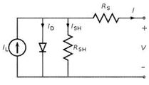
도 1a는, GaAs 태양 전지와 같은 화합물 반도체 또는 결정질 실리콘 태양 전지와 같은 일반적인 태양 전지의 등가 회로를 나타내는 개념도이다. 태양 전지는, 다이오드와 평행하여, 또한 분로 저항과 평행하게, 및 직렬 저항과 직렬로, 단락 전류 Isc(상기 태양 전지 말단이 짧을 경우에 흐르는 전류)으로 또한 알려지거나, IL로서 알려진 빛-발생 전류를 생산하는, 전류원으로서 나타낼 수도 있다(A solar cell may be represented as a current source, producing the photo-generation current shown as IL or also known as short circuit current Isc, in parallel with a diode, also in parallel with a shunt resistance, and in series with a series resistance). 전류원에 의해 생산된 상기 전류는, 상기 태양 전지 상에 태양광 조사 전력 강도(sunlight irradiation power intensity)의 레벨에 따라 다르다. 원하지 않는 암 전류 ID는 IL의 반대 방향(opposite direction)에서 흐르고, 상기 태양 전지에서 재결합 손실에 의해 생산된다. 이의 말단이 열리고, 어떠한 로드(any load)에 연결되지 않은 경우에, 상기 태양 전지를 가로지르는 전압은, Voc 또는 열린 회로전압(open-circuit voltage)으로서 알려져 있다. 현실적인 태양 전지 등가 회로는, 도 1b의 회로 도식도에서 나타낸 바와 같은, 한정된 직렬 저항 Rs 및 한정된 분로 저항 RSH을 또한 포함한다. 이상적인 태양 전지에서, 상기 직렬 저항 Rs는 제로이고, 상기 분로 저항 RSH는 무한하다. 그러나, 실제의 현실적인 태양 전지에서, 상기 유한한 직렬 저항은, 태양 전지가 이의 반도체 및 금속화에서 와류의 직렬 저항 구성요소(parasitic series resistance components)를 갖는 사실 때문이다(즉, 이는 완전 도체가 아니다). 반도체 층 저항 및 금속화 저항을 포함하는, 이러한 와류의 저항 구성요소는, 상기 태양 전지 작동 동안에 옴 손실(ohmic losses) 및 전력 손실을 결과적으로 야기한다. 상기 분로 저항은, 상기 태양 전지에서 그 밖의 비-이상적인 것 뿐만 아니라 지면 및 가장자리의 전환 결함과 같은 효과로 인하여 하나의 말단에서 다른 말단으로의 전류의 원하지 않는 누출에 의해 초래된다. 또다시, 이상적인 태양 전지는, 제로의 직렬 저항 및 유한한 저항 값의 분로 저항을 가질 것이다.
1A is a conceptual diagram showing an equivalent circuit of a general solar cell such as a compound semiconductor such as a GaAs solar cell or a crystalline silicon solar cell. Solar cells are, in parallel with the diode, and in parallel with the shunt resistor, and a series resistor in series, the short-circuit current Isc or also known as (the solar cell terminals current flows if short), also known as light as I L - generating (A solar cell may be represented as a current source, producing the photo-generation current as I L or also known as a short circuit current Isc, in parallel with a diode, also in parallel with a shunt resistance, and a series resistance. The current produced by the current source depends on the level of the sunlight irradiation power intensity on the solar cell. The unwanted dark current I D flows in the opposite direction of I L and is produced by the recombination loss in the solar cell. In the case where the end of this is open and not connected to any load, the voltage across the solar cell is known as Voc or an open-circuit voltage. A realistic solar cell equivalent circuit also includes a limited series resistance Rs and a limited shunt resistance R SH , as shown in the circuit diagram of Fig. 1b. In an ideal solar cell, the series resistance R s is zero, and the shunt resistor R SH is infinite. However, in practical realistic solar cells, the finite series resistance is due to the fact that solar cells have parasitic series resistance components in their semiconductors and metallizations (i.e. they are not perfect conductors) ). This vortex resistance component, including the semiconductor layer resistance and the metallization resistance, results in ohmic losses and power loss during the solar cell operation. The shunt resistors are caused by unwanted leakage of current from one end to another due to effects such as ground and edge switching defects as well as other non-idealities in the solar cell. Again, an ideal solar cell will have a series resistance of zero and a shunt resistance of a finite resistance value.
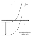
도 2a는, 또한 전류원, 빛-발생 전류, 및 암 전류를 나타내는(와류 직렬연결 및 분로 저항을 나타내지 않음), 상기 태양 전지의 등가 회로 모델을 나타내는 도식도이고, 도 2b는, 상기 전지 상의 태양광 일루미네이션(sunlight illumination)와 함께 및 상기 전지 상의 태양광 일루미네이션 없이, 결정질 실리콘 태양 전지와 같은 태양 전지의 전형적인 전류-전압(Ⅳ) 특성을 나타내는 이에 상응하는 그래프이다. IL 및 ID는, 각각 상기 태양 전지의 바람직한 빛-발생 전류 및 상기 바람직하지 않은 암 전류이다.
2A is a schematic diagram showing an equivalent circuit model of the solar cell showing a current source, a light-generating current, and a dark current (not showing an eddy series connection and shunt resistance), and Fig. (IV) characteristics of a solar cell, such as a crystalline silicon solar cell, with and without sunlight illumination on the cell. ≪ RTI ID = 0.0 > I L and I D are the desired light-generating current and the undesirable dark current of the solar cell, respectively.
PV 모듈에서 사용된 태양 전지는 필수적으로 포토다이오드(photodiodes)이다-이들은 상기 반도체 흡수체(semiconductor absorber)에서 빛-발생된 전하 캐리어(photo-generated charge carriers)를 통해 이들의 표면에 도달하는 태양광을 전력으로 직접적으로 전환한다. 복수의 태양 전지와 함께 모듈에서, 어떠한 그늘진 전지(any shaded cells)는, 상기 PV 모듈 내에 그늘지지 않은 전지(non-shaded cells)와 동일한 양의 전력을 생산할 수 없다. 일반적인 PV 모듈에서 상기 전지 모두가 직렬연결 스트링(series strings)에서 일반적으로 연결되기 때문에, 전류에서의 차이점은 또한 상기 전지(그늘진 vs 그늘지지 않은 전지)를 통해 빛-발생된 전류에서의 차이를 야기한다. 하나가 상기 그늘지지 않은 전지와 또한 직렬 연결된 그늘진(또는 부분적으로 그늘진) 전지를 통해 상기 직렬-연결된 그늘지지 않은 전지의 보다 높은 전류를 제공하도록 시도한다면, 상기 그늘진 전지(또는 부분적으로 그늘진 전지)의 전압은 실질적으로 부정적이다(즉, 그늘진 전지는 효율적으로 역방향으로 편향된다)[If one attempts to drive the higher current of the series-connected non-shaded cells through a shaded (or partically shaded) cell which is also connected in series with the non-shaded cells, the voltage of the shaded cell (or partially shaded cell) actually becomes negative (i.e., the shaded cell effectively becomes reverse biased)]. 이러한 역방향 바이어스 조건(this reverse bias condition) 하에서, 상기 그늘진 전지는, 전력을 생산하는 것 대신에 전력을 소비하거나 전력을 현저하게 소멸한다. 상기 그늘진 또는 사실상 그늘진 전지에 의해 소비되고 소멸되는 전력은, 상기 그늘진 전지가 위치하는 국한된 핫 스팟을 생성하고, 전지 및 모듈 고장을 궁극적으로 가능하고, 이런 이유로 상기 필드에서 주요한 신뢰성 고장 문제를 형성하는, 상기 전지를 가열하게 할 것이다(The power consumed and dissipated by the shaded or pratically shaded cell will cause the cell to heat up, creating a localized hot spot where the shaded cell is located, and eventually possibly causing cell and module failure, hence creating major reliability failure problems in the field).
The solar cells used in the PV modules are essentially photodiodes - they are photovoltaic cells that reach the surface of these through photo-generated charge carriers in the semiconductor absorber Directly switches to power. In modules with multiple solar cells, any shaded cells can not produce the same amount of power as non-shaded cells in the PV module. Since in the general PV module all of these cells are commonly connected in series series strings, the difference in current also causes a difference in the light-generated current through the battery (shaded vs. unshaded battery) do. If one attempts to provide a higher current through the shaded cell and also through the shaded (or partially shaded) cell in series with the shaded cell (or partially shaded cell) The voltage is substantially negative (that is, the shaded cell is effectively deflected in the opposite direction). [If one attempts to drive the higher current of the series-connected non-shaded cells through a shaded cell in series with the non-shaded cells, the voltage of the shaded cells (or partially shaded cells) actually becomes negative (ie, the shaded cells are reversed biased). Under this reverse bias condition, the shaded cell either consumes power or dissipates significant power instead of producing power. The power consumed by and consumed by the shaded or substantially shaded cells creates the localized hot spots where the shaded cells are located and is ultimately capable of battery and module failures and thus leading to major reliability failure problems in the field , Which will cause the battery to heat up. (The power consumed and dissipated by the shaded or pratically shaded cell will cause the cell to heat up, creating a localized hot spot where the shaded cell is located, resulting in major failure problems in the field.
표준(즉, 일반적으로 60 개의 태양 전지를 포함하는 PV 모듈) 결정질 실리콘 PV 모듈은, 상기 모듈 내에 세 개의 20-셀 직렬-연결된 스트링(three 20-cell series-connected strings) 내로 일반적으로 연결되고, 외부의 바이패스 다이오드[일반적으로 pn 접합 다이오드(pn junction diode) 또는 쇼트키 다이오드(Schottky diode)]에 의해 보호된 각각은, 상기 직렬-연결된 모듈의 외부의 전기 리드 및 상기 최종의 PV 모듈 조립체 전기적인 상호 연결을 형성하기 위해, 서로 직렬로 전기적으로 연결된 외부의 접합 박스(external junction box)에 위치된다. 상기 PV 모듈이 이의 표면 상의 상대적으로 균일한 태양 조사(solar irradiation)를 받는 동안에, 상기 모듈 내의 상기 전지는, 대부분의 결정질 실리콘 PV 모듈을 위해 대략 ~ 0.5 V 내지 0.6 V에 따라, Vmp 또는 전지 최대-전력 전압과 함께, 거의 동일한 양의 전력(및 전기적인 전류)를 생산할 것이다. 이런 이유로, 직렬로 연결된 20 개의 전지의 각각의 스트링을 따라 상기 최대-전력 전압 또는 Vmp는, 결정질 실리콘 전지를 사용하여 PV 모듈에 대해 대략 10 내지 12 V에 따를 것이다(Hence, the maximum-power voltage or Vmp across each strong of 20 cells connected in series will be approximately on the order of 10 to 12 V for a PV module using crystalline silicon cells). 상기 균일한 모듈 일루미네이션 조건(module illumination condition) 하에서, 각각의 외부의 바이패스 다이오드는 이의 말단을 따라 약 -10 내지 -12 V 역방향 바이어스 전압을 가질 것이고(상기 모듈은 이의 최대-전력점 또는 MPP에서 작동하면서), 상기 바이패스 다이오드는 상기 OFF 상태로 남아있다(이런 이유로, 상기 접합 박스에서 상기 역방향의 편향된 외부의 바이패스 다이오드에 의해 상기 모듈 전력 출력 상에서 어떠한 영향도 없다). 20 개-전지 스트링에서의 전지가 부분적으로 또는 완전하게 그늘진 경우에, 이는 상기 그늘지지 않는 전지보다 더 낮은 전력(및 보다 낮은 전류)를 생산한다. 상기 스트링에서 상기 전지가 연속하여 일반적으로 연결되기 때문에, 상기 그늘진 태양 전지는 역방향으로 편향되고(the shaded solar cell becomes reverse biased), 전력을 소멸하기 시작하고, 따라서 전력을 생산하는 것 대신에, 상기 역방향-편향된 그늘진 전지의 위치에서 국한된 핫 스팟을 생산할 것이다. 적절한 예방조치가 취해지지 않는 한, 상기 그늘진 전지의 상기 전력 소멸 및 결과적으로 국소화된 가열은, 상기 설치된 PV 시스템에서 잠재적인 화재 위험 뿐만 아니라, 다양한 고장 모드[역방향-편향된 그늘진 전지의 고장, 전지-대-전지 상호연결의 고장, 및/또는 상기 봉합재(encapsulant) 및/또는 백 시트(backsheet)와 같은 상기 모듈 라미네이트 물질(module lamination materials)의 고장과 같은]로 인한 좋지 못한 전지 및 모듈 신뢰성(module reliability)을 야기할 수도 있다.
A standard (i. E., A PV module typically comprising 60 solar cells) crystalline silicon PV modules are generally connected into three 20-cell series-connected strings within the module, Each protected by an external bypass diode (typically a pn junction diode or a Schottky diode) is connected to the external electrical leads of the series-connected module and to the final PV module assembly electrical Are placed in an external junction box that is electrically connected in series with one another to form an interconnect. While the PV module is undergoing a relatively uniform solar irradiation on its surface, the battery in the module may have a V mp or cell voltage of about < RTI ID = 0.0 > Along with the maximum-power voltage, will produce approximately the same amount of power (and electrical current). For this reason, the maximum-power voltage or V mp along each string of twenty batteries connected in series will be approximately 10-12 V for the PV module using a crystalline silicon cell (Hence, the maximum-power voltage or V mp across each of the 20 cells connected in series will be approximately 10 to 12 V for a PV module using crystalline silicon cells. Under this uniform module illumination condition, each external bypass diode will have a reverse bias voltage of about -10 to -12 V along its end (the module has its maximum-power point or MPP The bypass diode remains in the OFF state (for this reason there is no effect on the module power output by the reverse biased external bypass diode in the junction box). 20 - If the cell in the cell string is partially or completely shaded, it produces lower power (and lower current) than the non-shaded cell. Since the cells in the string are generally connected in series, the shaded solar cells are biased in reverse and the shaded solar cells become reversed biased and start to dissipate power, so instead of producing power, Will produce a localized hot spot at the location of the reverse-biased shaded cell. The power dissipation and consequent localized heating of the shaded cell, as long as adequate precautions are not taken, can result in a variety of failure modes (failure of a reverse-deflected shaded cell, battery- (Such as failure of the module-lamination material, such as failure of the battery-to-cell interconnect, and / or encapsulant and / or backsheet) module reliability.
결정질 실리콘 모듈은, 전지의 부분적인 또는 완전한 그늘짐(full shading)에 의해 야기되는 상기에 언급된 핫-스팟 효과(hot-spot effects)를 제거하고, 상기 결과적으로 야기된 잠재적인 모듈 신뢰성 고장을 예방하기 위해 외부의 바이패스 다이오드를 종종 사용한다. 상기 그늘진 전지의 역방향 편향(reverse biasing)에 의해 야기되는, 이러한 핫-스팟 현상은, 상기 영향을 미치는 PV 전지를 주로 손상시킬 것이고, 만약 PV 모듈에서 상기 PV 전지의 상기 표면에 도달하는 태양광이 현저하게 균일하지 않으면(예를 들어, 하나 또는 그 이상의 전지의 완전한 또는 심지어 부분적인 그늘짐으로 인하여), 심지어 화재 위험을 초래한다. 바이패스 다이오드는, 세 개의 20-전지 서브-스트링과 함께, 표준 60 개-전지 결정질 실리콘 태양 모듈에서 20 개의 태양 전지의 서브-스트링 당 일반적으로 하나의 외부의 바이패스 다이오드, 상기 PV 모듈의 서브-스트링 상에 일반적으로 설치된다(Bypass diodes are usually placed on sub-strings of the PV module, typically one external bypass diode per sub-string of 20 solar cells in a standard 60-cell crystalline silicon solar module with three 20-cell sub-strings)(이러한 배열은, 세 개의 24 개-전지 서브-스트링과 함께 72 개-전지 결정질 실리콘 태양 모듈에서 24 개의 태양 전지의 서브-스트링 당 하나의 외부 바이패스 다이오드일 수도 있다; 많은 그 밖의 배열은 수많은 전지와 함께 모듈에 대해 가능하다). 상기 직렬-연결된 전지 스트링을 따라 외부의 바이패스 다이오드 이러한 연결 배열은 역방향 바이어스 핫 스팟을 예방하고, 상기 PV 모듈은 다양한 실생활의 그늘짐 또는 부분적인 그늘짐 및 솔링 조건(soling conditions) 하의 이들의 수명 동안에 높은 신뢰성과 함께 작용하도록 한다. 전지의 그늘짐이 없는 경우에, 상기 스트링에서 각각의 전지는, 상기 모듈에서 상기 서브-스트링의 전체적인 전압과 함께 역방향의 편향된 상기 서브-스트링에서 상기 외부의 바이패스 다이오드와 함께, 상기 스트링에서 그 밖의 전지와 함께 상대적으로 일치된 전류 값과 함께 전류원으로서 작용한다(In the absence of cell shading, each cell in the string acts as a current source with relatively matched current values with the other cells in the strong, with the external bypass diode in the sub-string being reversed biased with the total voltage of the sub-string in the module)(예를 들어, 직렬로 20 개의 전지는, 결정질 실리콘 PV 시스템에서 상기 바이패스 다이오드를 따라 대략 10 V 내지 12 볼트 역방향 바이어스를 생산한다). 스트링에서 전지의 그늘짐과 함께(With shading of a cell in a strong), 상기 그늘진 전지는 상기 그늘진 전지를 포함하는 상기 서브-스트링을 위한 상기 바이패스 다이오드 상에 방향전환하는, 역방향으로 편향되고, 이로 인하여 상기 외부의 바이패스 회로에서 흐르기 위해, 상기 그늘지지 않은 서브-스트링에서 좋은 태양 전지로부터의 전류를 가능하게 한다(With shading of a cell in a strong, the shaded cell is reverse biased, turning on the bypass diode for the sub-string containing the shaded cell, thereby allowing the current from the good solar cells in the non-shaded sub-strings to flow in the external bypass circuit). 상기 외부의 바이패스 다이오드(일반적으로 세 개의 외부의 바이패스 다이오드는 60 개-전지 결정질 실리콘 PV 모듈 접합 박스에서 포함된다)가 상기 전지의 그늘짐의 경우에서 상기 PV 모듈 및 전지를 보호하면서, 이들은 실질적으로, 상기 설치된 PV 시스템에 대해 전력 획득 및 에너지 수득의 현저한 손실을 또한 야기할 수 있다.
The crystalline silicon module eliminates the above-mentioned hot-spot effects caused by partial or complete shading of the battery and reduces the resulting potential module reliability failure An external bypass diode is often used to prevent this. This hot-spot phenomenon, caused by the reverse biasing of the shaded cells, will primarily damage the PV cells that have this effect, and if the sunlight reaching the surface of the PV cell in the PV module (For example, due to complete or even partial shading of one or more batteries), even resulting in a fire hazard. The bypass diodes, together with three 20-cell sub-strings, typically have one external bypass diode per sub-string of 20 solar cells in a standard 60-cell crystalline silicon solar module, (Bypass diodes are usually placed on the PV modules, typically one external bypass diode per sub-string of 20 solar cells in a standard 60-cell crystalline silicon solar module with three 20- cell sub-strings (this arrangement may be one external bypass diode per sub-string of 24 solar cells in a 72-cell crystalline silicon solar module with three 24-cell sub-strings; many Other arrangements are possible for the module with numerous batteries). Such an interconnected arrangement of external bypass diodes along the series-connected battery strings prevents reverse bias hot spots, and the PV modules are capable of preventing their lifetime under various realistic shade or partial shade and soling conditions To work together with high reliability. In the absence of shading of the battery, each battery in the string, together with the external bypass diode in the reverse biased sub-string together with the overall voltage of the sub-string in the module, With the current value being relatively coincident with the external cell (the cell current acts as a current source with a relatively large current value, (for example, twenty batteries in series may be used in a crystalline silicon PV system along the bypass diode at about 10 V to about < RTI ID = 0.0 > Producing a 12 volt reverse bias). Wherein the shaded cell is deflected in the reverse direction to redirect onto the bypass diode for the sub-string comprising the shaded cell, with the shading of the cell in a strong, Thereby enabling current from a good solar cell in the unshaded sub-string to flow in the external bypass circuit (with shading of a cell in a strong, the shaded cell is reversed biased, turning on the bypass diode for the sub-string containing the shaded cell, allowing the current to flow from the solar cell to the non-shaded sub-strings to the external bypass circuit. While the external bypass diode (typically three external bypass diodes are included in the 60-cell crystalline silicon PV module junction box) protects the PV module and the battery in the event of shading of the battery, Substantially, it can also cause a significant loss of power acquisition and energy gain for the installed PV system.
도 3a 및 3b는, 상기 모듈에서 어떠한 전지의 그늘짐 또는 과량의 부분적인 그늘짐 동안에 상기 전지를 보호하기 위해, 세 개의 외부의 바이패스 다이오드(4), 및 직렬로 연결된 세 개의 20 개-전지 서브-스트링(2)과 함께 대표적인 60 개-전지 결정질 실리콘 태양 모듈(직렬로 연결된 각각의 서브-스트링에서 20 개의 전지와 함께)의 도표이다[도 3a는 단일-전지 그늘짐, 그늘진 전지(6)을 나타내고, 도 3b는 다수-전지 부분적인 그늘짐 조건, 부분적으로 그늘진 열(8)을 나타낸다]. 예로서, 도 3a는 하부의 열에서 1 개의 그늘진 전지를 갖는 60 개-전지 모듈(그늘짐에 의해 영향을 받은 하나의 20 개-전지 서브-스트링)을 나타내고, 도 3b는, 하부의 열에서 6 개의 부분적으로 그늘진 전지를 갖는 60 개-전지 모듈(그늘짐에 의해 영향을 받은 3 개의 20 개-전지 서브-스트링)을 나타낸다. 만약 하나 또는 그 이상의 전지가 서브-스트링에서 그늘진다면(또는 그늘짐의 현저한 정도로 부분적으로 그늘진다면)(도 3a에 나타낸 바와 같음), 상기 그늘진 전지(들)을 갖는 상기 서브-스트링을 위한 상기 바이패스 다이오드는, 전체의 서브-스트링을 활성화하고, 전환하고(shunts), 따라서 상기 핫 스팟을 예방하고, 또한 약 1/3로 효과적인 모듈 전력 산출량을 감소시킴으로써 상기 그늘진 전지를 둘 다 보호한다(만약 세 개의 서브-스트링 중의 오직 하나만이 그늘짐에 의해 영향을 받는다면). 만약 서브-스트링 당 적어도 하나의 전지가 그늘진다면(도 3b에 나타낸 바와 같음), 세 개의 바이패스 다이오드 모두가 활성화되고, 상기 전체 모듈을 전환하고, 따라서 상기 세 개의 20개-전지 서브-스트링의 각각에서 적어도 하나의 그늘진 전지가 있는 경우에, 상기 모듈로부터 어떠한 전력의 추출을 예방한다(If at least one cell per sub-string is shaded, all three bypass diodes are activated and shunt the entire module, thus preventing extraction of any power from the module when there is at least one shaded cell in each of the three 20-cell sub-strings).
Figures 3a and 3b show three external bypass diodes (4) and three 20-cell modules connected in series to protect the battery during shade or excessive partial shade of any cell in the module. Is a plot of a representative 60-cell crystalline silicon solar module (with 20 cells in each sub-string connected in series) with a sub-string 2 (Figure 3a shows a single-cell shaded, shaded
예로서, 전형적인 외부의 PV 모듈 접합 박스는, 60 개-전지 결정질 실리콘 태양 모듈에서 세 개의 외부의 바이패스 다이오드를 제공할 수도 있다. 상기 외부의 접합 박스 및 관련된 외부의 바이패스 다이오드는 상기 전체적인 PV 모듈 자재표(Bill of Materials, BOM) 비용의 일부에 기여하고, 상기 PV 모듈 비용(즉, 태양 전지의 비용을 제외한 상기 PV 모듈 BOM 비용의 퍼센트로서)의 약 10 %에 기여할 수도 있다. 게다가, 상기 외부의 접합 박스는, 상기 설치된 PV 시스템에서 필드 신뢰성 고장 및 화재 위험의 원인일 수도 있다(Moreover, the external junction box may also be a source of field reliability failures and fire hazards in the installed PV systems). 대부분의 전류 결정질 실리콘 PV 모듈이 주로, 상기 접합 박스에 위치된 외부의 바이패스 다이오드와 함께 외부의 접합 박스를 사용하면서, 상기 PV 모듈 조립체 내로 직접적으로 상기 세 개의 바이패스 다이오드를 배치하고 라미네이트하는 전면-접촉 전지(front-contact cells)를 갖는 PV 모듈의 몇몇의 예가 있지만, 상기 모듈 라미네이트 공정 동안에, 상기 전면-접촉 태양 전지로부터 분리된다(그러나, 여전히 전면-접촉 전지의 20 개-전지 서브-스트링 당 하나의 바이패스 다이오드를 사용하여). 이러한 예는 외부의 바이패스 다이오드의 라미네이트를 여전히 갖고, 즉, 단일 전지가 그늘진 경우에, 상기 바이패스 다이오드는 상기 서브-스트링 내로 상기 그늘진 전지를 갖는 전지의 전체적인 서브스트링을 전환하고, 따라서 상기 설치된 PV 시스템의 에너지 수득 능력 및 전력 수집을 감소시킨다(This example still has the limitations of external bypass diodes, i.e., even when a single cell is shaded the bypass diode shunts the entire substring of cells with the shaded cell within the sub-string thus reducing the power harvesting and energy yield capability of the installed PV system).
By way of example, a typical external PV module junction box may provide three external bypass diodes in a 60-cell crystalline silicon solar module. The external junction box and the associated external bypass diode contribute to a portion of the overall PV module bill of materials (BOM) cost, and the PV module cost (i. E., The PV module BOM As a percentage of the cost). In addition, the external junction box may be a cause of field reliability failure and fire risk in the installed PV system (additionally, the external junction box may also be a source of field reliability failures and fire hazards in the installed PV systems) . Most current crystalline silicon PV modules are mainly used to place the three bypass diodes directly into the PV module assembly and to laminate the front side of the PV module assembly using an external junction box with an external bypass diode located in the junction box, There are some examples of PV modules with front-contact cells, but during the module lamination process, they are separated from the front-contacting solar cells (however, still the 20-cell sub- Using one bypass diode per one). This example still has an external bypass diode laminate, i. E. When the single cell is shaded, the bypass diode switches the entire substring of the cell with the shaded cell into the sub-string, This reduces the energy harvesting capability and power collection of the PV system. (This example also shows that the bypass diodes are shaded even when a single cell is shaded with the entire substring of cells with the shaded cell within the sub- and thus the power harvesting and energy yield capability of the installed PV system.
모듈의 직렬연결 스트링에서 모듈 상의 그늘짐의 신뢰성 고장 효과를 최소화하기 위한 하나의 알려진 방법은, 직렬로 연결된 모듈을 따라 바이패스 다이오드를 사용하는 것이고, 이의 효과는 도 4a 및 4b에서 나타내었고, 회로의 예는 도 5에 기재되어 있다(One known method to minimize the reliability failure effects of shading on a module in a series string of modules is to use bypass diodes across modules connected in series, the effect of which is shown in Figs. 4A and 4B and an example circuit is depicted in Fig. 5). 이는 각각의 모듈 접합 박스 내의 외부의 바이패스 다이오드를 갖는 모듈과 동일한 효과에 있다. 도 4a는 태양 전지 모듈 직렬연결(solar cell module series)을 위한 그늘지지 않은 전류로(current path)를 나타내고, 도 4b는, 대체적인 전류로(alternative current path)를 제공하는 바이패스 다이오드 및 그늘진 하나의 모듈을 갖는 동일한 태양 전지 모듈 직렬연결을 나타낸다. 그리고 도 5는, 모듈 서브-스트링 또는 스트링에서 사용된 외부의 바이패스 다이오드를 갖는 직렬-연결된 태양 전지의 도식적인 회로 모델 도표이다(각각의 태양 전지는 이의 동등한 회로도와 함께 나타냄). 상기 어떠한 전지도 그늘지지 않았다면, 상기 바이패스 다이오드는 상기 역방향 바이어스 상태로 남아있고, 상기 태양 전지 스트링은, 상기 태양 모듈 전력 발생에 완전히 기여하게, 정상적으로 작동한다. 상기 전지의 어떠한 것이 부분적으로 또는 완전하게 그늘진다면, 상기 그늘진 전지는 역방향으로 편향되고, 상기 바이패스 다이오드는 정방향으로 편향되고, 이런 이유로, 상기 그늘진 전지에 대한 손상 또는 핫 스팟의 가능성을 최소화한다. 다시 말해서, 모듈이 그늘진 경우에, 이의 바이패스 다이오드는 정방향으로 편향되고, 모듈의 직렬연결 스트링에서 신뢰성 문제 및 성능 저하를 예방하는 전류를 처리한다. 상기 바이패스 다이오드는, 상기 모듈 스트링 배열 산출량에서 전체적인 전력 감소를 제한하는, 상기 전체 그늘진 모듈(또는 적어도 하나의 그늘진 전지를 갖는 서브-스트링)의 전압을 작은 네거티브 전압(small negative voltage)(예를 들어, -0.5V 내지 0.7V)으로 유지한다.
One known method for minimizing the reliability failure effect of shading on a module in a series connection string of a module is to use a bypass diode along a series connected module whose effect is shown in Figures 4a and 4b, FIG. 5 shows an example of the method of the present invention. FIG. 5 shows one example of a method for minimizing the reliability of a module. 4A and 4B and an example circuit is depicted in Fig. This has the same effect as a module having an external bypass diode in each module junction box. 4A shows a non-shadowed current path for a solar cell module series, and FIG. 4B shows a bypass diode and a shaded one that provide an alternative current path. Lt; RTI ID = 0.0 > module. ≪ / RTI > And Figure 5 is a schematic circuit model diagram of a series-connected solar cell with an external bypass diode used in a module sub-string or string (each solar cell is shown with its equivalent circuit diagram). If none of the cells are shadowed, the bypass diode remains in the reverse biased state, and the solar cell string operates normally, contributing fully to the solar module power generation. If any of the cells are partially or completely shaded, the shaded cells are deflected in the reverse direction, and the bypass diodes are deflected in the forward direction, thereby minimizing the possibility of damage or hot spot to the shaded cell. In other words, when the module is shaded, its bypass diode is deflected in the forward direction to handle currents that prevent reliability problems and performance degradation in the serial connection string of the module. The bypass diode is configured to convert the voltage of the entire shaded module (or the sub-string having at least one shaded cell) to a small negative voltage (e.g., For example, -0.5 V to 0.7 V).
도 6은, (pn 접합 바이패스 다이오드와 함께 나타낸 예) 바이패스 다이오드와 함께 및 바이패스 다이오드 없는 결정질 태양 전지의 전류-전압(I-V) 특성을 나타낸 그래프이다. 상기 바이패스 다이오드는, 그늘진 태양 전지를 따라 최대한의 역방향 바이어스 전압을 상기 바이패스 다이오드의 단지 켜진 정방향 바이어스 전압으로 제한한다(The bypass diode limits the maximum reverse bias voltage applied across a shaded solar cell to no more than the turn-on forward bias voltage of the bypass diode).
6 is a graph showing the current-voltage (IV) characteristics of a crystalline solar cell with and without a bypass diode (example shown with a pn junction bypass diode). The bypass diode limits the maximum reverse bias voltage along the shaded solar cell to only the on-state forward bias voltage of the bypass diode (the bypass diode limits the maximum reverse bias voltage applied across the shaded solar cell to no more than the turn-on forward bias voltage of the bypass diode.
도 7은, 60 개-전지 모듈 내로 20 개-전지 서브-스트링 당 하나의 그늘진 전지[그늘진 전지(10)과 같은, 세 개의 전지가 전체적으로 그늘져 있다]를 갖는 도 4 및 5와 유사한 결정질 실리콘 PV 모듈의 예를 나타낸 도표이고, 세 개의 20 개-전지 서브-스트링이 상기 그늘진 전지를 보호하기 위해 상기 바이패스 다이오드에 의해 바뀌기 때문에, 상기 세 개의 20 개-전지 서브-스트링에서 상기 세 개의 그늘진 전지가 상기 모듈에 의해 제공된 태양 PV 전력의 제거를 야기한다. 20 개-전지 서브-스트링 당 하나의 외부의 바이패스 다이오드의 배열을 사용하는 것은, 상기 세 개의 20 개-전지 서브-스트링에서 세 개의 그늘진 전지를 갖는 결과가, 상기 PV 모듈의 단지 3/60(60 개의 전지 중의 3 개)가 그늘짐에 의해 영향을 받을지라도, 상기 PV 모듈로부터 추출된 상기 전력이 제로로 떨어지는 것이다. 한번 더, 외부의 바이패스 다이오드를 갖는 공지된 PV 모듈 배열의 이러한 타입은, 상기 필드에서 상기 설치된 PV 시스템에 대해 현저한 에너지 수득 및 전력 수확 패널티(power harvesting penalty)를 야기한다.
Figure 7 shows a cross-sectional view of a crystalline silicon < RTI ID = 0.0 > (Si) < / RTI & PV module, and since three 20-cell sub-strings are changed by the bypass diode to protect the shaded cell, the three shaded cells in the three 20-cell sub- The battery causes removal of the solar PV power provided by the module. Using an arrangement of one external bypass diode per 20 cell sub-strings means that the result of having three shaded cells in the three 20-cell sub-strings is only 3/60 of the PV module (3 out of 60 cells) are affected by shading, the power extracted from the PV module drops to zero. Once again, this type of known PV module arrangement with an external bypass diode results in a significant energy gain and power harvesting penalty for the installed PV system in the field.
다수의 모듈 스트링을 갖는 결정질 실리콘 PV 시스템 설비에서, 전력 수확 및 에너지 수득에서의 상기 모듈 그늘짐 효과(module shading effects) 및 이의 해로운 영향은, 모듈의 단일 직렬연결 스트링(single series string)을 갖는 상기에 나타낸 예보다 보다 클 수도 있다. 직렬 연결된 모듈 스트링의 다수의 평행한 스트링을 갖는 PV 시스템(PV systems with multiple parallel strings of series connected module strings)에서, 상기 병렬 스트링은 서로 대략 동일한 전압을 생성하여야 한다(즉, 병렬 스트링의 전압은 일치되어야 한다). 결과적으로, 대략 동일한 전압에서 작동하는 병렬로 연결된 모든 모듈 스트링을 갖는 것의 전기적인 제약은 그늘진 스트링이 이의 바이패스 다이오드를 활성화하는 것을 가능하게 하지 않는다. 따라서, 많은 경우에, 상기 스트링 중의 하나에서 PV 모듈 상의 그늘은, 전체적인 스트링에 의해 생성된 상기 전력을 실질적으로 줄일 수도 있다. 대표적인 예로서, 상기 예에서 기재된 바와 같은 그늘진 하나의 PV 모듈 스트링 및 하나의 그늘지지 않은 PV 모듈 스트링을 고려한다. 최대-전력점-추적(Maximum-Power-Point-Tracking, MPPT) 능력은, 상기 제1 PV 모듈 스트링으로부터의 최대의 전력의 생산 및 상기 제2 PV 모듈 스트링으로부터의 70 %의 최대의 전력의 생산을 할 수 있게 할 것이다. 이러한 방식으로, 스트링 둘 다는 동일한 전압에 도달한다[상기 병렬 스트링으로부터의 전류가 직렬-연결된 모듈의 상기 병렬 연결된 스트링에 대한 동일한 모듈 스트링 전압에 부가적이다]. 따라서, 집중된 MPPT와 함께 집중된 DC-to-AC 인버터를 사용하는 것 및 이러한 예에서, 상기 PV 모듈 배열에 의해 생산된 전력은, 어떠한 모듈 그늘짐(any module shading) 없이 최대 가능한 전력의 85 % 일 것이다.
In crystalline silicon PV system installations with multiple module strings, the module shading effects and their detrimental effects on power harvesting and energy yields can be minimized with the use of a single series string of modules May be larger than the example shown in Fig. In a PV system with multiple parallel strings of series connected module strings, the parallel string must produce approximately the same voltage as each other (i.e., the voltage of the parallel string is matched . As a result, the electrical constraint of having all the module strings connected in parallel operating at approximately the same voltage does not make it possible for the shaded strings to activate their bypass diodes. Thus, in many cases, the shade on the PV module in one of the strings may substantially reduce the power generated by the overall string. As a representative example, consider a shade one PV module string and one unshaded PV module string as described in the above example. The maximum-power-point-tracking (MPPT) capability is defined as the production of maximum power from the first PV module string and the production of a maximum of 70% power from the second PV module string To do so. In this way, both strings reach the same voltage (current from the parallel string is additive to the same module string voltage for the parallel-connected string of the series-connected module). Thus, using DC-to-AC converters centralized with centralized MPPT, and in this example, the power produced by the PV module array is 85% of the maximum possible power without any module shading will be.
도 8 및 9는, PV 시스템 설비의 두 개의 예를 나타내는 도표이다. 도 8 은, 600 V, 900 W PV 출력(output)을 생산하기 위해 연결된 바이패스 다이오드를 갖는 3 x 6 배열의 PV 모듈(각각은 50 W 출력을 가짐)의 예를 나타낸 것이다. 도 9 는,충전 베터리와 함께 바이패스 다이오드 및 차단 다이오드(blocking diode)를 갖는 3 PV 모듈의 직렬 연결(series connection)을 나타낸 것이다. 통상적인 모듈에서, 직렬 및 병렬 연결된 모듈 스트링(module strings connected in series and in parallel)은, 일반적으로 바이패스 및 차단 다이오드를 사용할 수도 있다. 그러나, 상기에 기재된 예와 유사하게, 이러한 대표적인 PV 모듈 설비는, 상기에 서술된 문제로 인하여 상기 설비된 PV 시스템의 에너지 수득을 감소시키고, 상기 전력 수확 제한을 당한다.
Figures 8 and 9 are charts illustrating two examples of PV plant installations. Figure 8 shows an example of a 3 x 6 array of PV modules (each with a 50 W output) with a bypass diode connected to produce a 600 V, 900 W PV output. Figure 9 shows a series connection of 3 PV modules with bypass diodes and blocking diodes with a rechargeable battery. In a typical module, module strings connected in series and in parallel may generally use bypass and isolation diodes. However, similar to the example described above, this exemplary PV module installation reduces the energy yield of the installed PV system due to the problems described above, and is subject to the power harvest limit.
집중기 PV(또는 CPV) 적용을 위한 전면-접촉, 화합물 반도체(Ⅲ-Ⅴ), 다중-접합 태양 전지(multi-junction solar cell)를 갖는 바이패스 다이오드의 모놀리식 집적화(monolithic integration)의 또 다른 대표적인 예. 도 10은, 다중-접합 화합물 반도체 CPV 전지를 갖는 바이패스 다이오드의 모놀리식 집적화의 예를 나타내는 도표이다. 이러한 예는, CPV 적용을 위한 다중-접합 태양 전지, 화합물 반도체로서의 동일한 저마늄 (Ge) 기판 상의 모놀리식으로 집적된(monolithically integrated) 바이패스 다이오드로서 사용된 화합물 반도체 쇼트키 다이오드를 나타낸다. 이러한 예에서, 상기 쇼트키 다이오드 및 상기 화합물 반도체, 다중-접합 태양 전지는 상기 태양 전지의 상기 동일한 면[윗 면(top side)] 상에 둘 다 있고, 상이한 물질 층 스택(different material layer stacks)을 가지고, 이렇게 함으로써 보다 복잡하고 많은 돈이 드는 상기 태양 전지 제조 공정이 제조되었다(이런 이유로, 이러한 실시형태는 오직 상기 CPV 전지가 비싼 상기 CPV 적용을 위해 요구된다). 상기 동일한 비싼 저마늄 기판 상에서 상기 태양 전지를 갖는 상기 쇼트키 바이패스 다이오드의 모놀리식 집적화의 결과로서, 상기 전체적인 공정 복잡성 및 비용은, 상기 전지의 활성화된 서니사이드로서(as the active sunnyside of the cell) 동일한 면 상의 상기 쇼트키 바이패스 다이오드의 집적화로 인하여, 효율적인 태양 전지 및 태양 패널 효율성 패널티(solar panel efficiency penalty)를 초래하면서, 실질적으로 추가적으로 증가된다. 전면-접촉 화합물 반도체 다중-접합 태양 전지 상의 상기 바이패스 쇼트키 다이오드의 이러한 모놀리식 집적화는, 상기 바이패스 스위치에서 및 상기 태양 전지에서 물질 층의 상이한 스택을 필요로 하고, 이런 이유로 상기 전체적인 모놀리식 태양 전지 프로세싱(processing)을 실질적으로 복잡하게 하고, 태양 전지 제조 공정 단계의 수를 증가시키고, 이의 제조 비용을 증가시킨다. 상기 태양 전지의 제조를 위한 이러한 현저한 추가된 프로세싱의 복잡성 및 비용 증가가, CPV 태양 전지에서 용인될 수도 있으면서, 이는 결정질 실리콘 태양 전지에서와 같은 비-매우 높은 농도(non-very high concentration)-CPV 태양 전지에서 경제적으로 실행가능할 수 없다. 도 11은, 다중-접합 화합물 반도체 CPV 전지를 갖는 바이패스 다이오드의 모놀리식 집적화의 예를 나타낸 도표이다. 이러한 예는, 다중-접합 태양 전지, 화합물 반도체로서 상기 동일한 저마늄 (Ge) 기판 상의 모놀리식으로 집적된 바이패스 다이오드로서 사용된 pn 접합 다이오드를 나타낸다. 이러한 예에서, 상기 pn 접합 바이패스 다이오드 및 상기 화합물 반도체, 다중-접합 태양 전지는 상기 태양 전지의 상기 동일한 면(윗 면) 상에 둘 다 있고, 상이한 물질 스택을 가지고, 이로 인하여 상기 태양 전지 제조 공정이 보다 복잡하고 비용이 많이 든다(이런 이유로, 이러한 실시형태는 오직 상기 CPV 전지가 비싼 상기 CPV 적용을 위해 요구된다). 상기 동일한 비용이 비싼 저마늄 기판 상의 상기 태양 전지를 갖는 상기 pn 접합 바이패스 다이오드의 모놀리식 집적화의 결과로서, 상기 전체적인 공정 복잡성 및 비용이 추가적으로 증가되면서, 상기 전지의 상기 활성 서니사이드로서 상기 동일한 면 상의 상기 바이패스 다이오드의 집적화로 인하여 태양 패널 효율성 패널티 및 효과적인 태양 전지를 초래한다(while incurring an effective solar cell and solar panel efficiency penalty due to the integration of the bypass diode on the same side as the active sunnyside of the cell). 또다시, 전면-접촉 화합물 반도체 다중-접합 태양 전지 상의 상기 바이패스 pn 접합의 이러한 모놀리식 집적화는, 상기 바이패스 스위치에서 및 상기 태양 전지에서 물질 층의 상이한 스택을 필요로 하고, 이런 이유로 상기 전체적인 모놀리식 태양 전지 공정을 실질적으로 복잡하게 하고, 태양 전지 제조 공정 단계의 수를 증가시키고, 이의 제조 비용을 증가시킨다. 상기 태양 전지의 제조를 위한 이러한 현저한 추가된 공정의 복잡성 및 비용 증가가, CPV 태양 전지에서 용인될 수도 있으면서, 이는 결정질 실리콘 태양 전지에서와 같은 비-매우 높은 농도(non-very high concentration)-CPV 태양 전지에서 경제적으로 실행가능할 수 없다.
The monolithic integration of bypass diodes with front-contact, compound semiconductors (III-V), multi-junction solar cells for concentrator PV (or CPV) Another representative example. 10 is a diagram showing an example of monolithic integration of a bypass diode having a multi-junction compound semiconductor CPV cell. This example shows a compound semiconductor Schottky diode used as a monolithically integrated bypass diode on a multi-junction solar cell for CPV application, the same germanium (Ge) substrate as a compound semiconductor. In this example, the Schottky diode and the compound semiconductor, multi-junction solar cell are both on the same side (top side) of the solar cell and have different material layer stacks, (For this reason, this embodiment is required only for the CPV application where the CPV battery is expensive). As a result of the monolithic integration of the Schottky bypass diode with the solar cell on the same expensive low-germanium substrate, the overall process complexity and cost are reduced as the active sunnyside of the cell cell integration of the Schottky bypass diode on the same plane, resulting in an effective solar cell and solar panel efficiency penalty. This monolithic integration of the bypass Schottky diode on the front-facing compound semiconductor multi-junction solar cell requires a different stack of material layers in the bypass switch and in the solar cell, Which substantially complicates the artificial solar cell processing, increases the number of solar cell manufacturing process steps, and increases its manufacturing cost. While this significant additional processing complexity and cost increase for the fabrication of the solar cell may be tolerated in CPV solar cells, it is possible to use a non-very high concentration-CPV It can not be economically viable in solar cells. 11 is a diagram showing an example of monolithic integration of a bypass diode having a multi-junction compound semiconductor CPV cell. This example shows a pn junction diode used as a monolithically integrated bypass diode on the same germanium (Ge) substrate as a multi-junction solar cell, compound semiconductor. In this example, the pn junction bypass diode and the compound semiconductor, multi-junction solar cell are both on the same side (top surface) of the solar cell and have different stacks of materials, The process is more complicated and costly (for this reason, this embodiment is required only for the CPV application where the CPV battery is expensive). As a result of the monolithic integration of the pn junction bypass diodes with the solar cells on the same costly germanium substrate, the overall process complexity and cost are further increased, The integration of the bypass diode on the surface results in a solar panel efficiency penalty and an effective solar cell (while incurring an effective solar cell and solar panel efficiency penalty due to the integration of the bypass diode on the same side as the active sunnyside of the cell). Again, this monolithic integration of the bypass pn junction on the front-facing compound semiconductor multi-junction solar cell requires a different stack of material layers in the bypass switch and in the solar cell, Substantially complicates the overall monolithic solar cell process, increases the number of solar cell manufacturing process steps, and increases its manufacturing cost. While this significant additional process complexity and cost increase for the fabrication of the solar cell may be tolerated in CPV solar cells, it may be desirable to use a non-very high concentration-CPV It can not be economically viable in solar cells.
일반적으로, 매우 높은 농도 CPV 적용을 위한 비용이 비싼 다중-접합 태양 전지 상에 나타낸 바와 같은 상기 바이패스 다이오드의 상기 모놀리식 집적화(쇼트키 다이오드 또는 pn 접합 다이오드)는, 상기 태양 전지와 함께 상기 모놀리식 집적화의 추가된 제조 공정 복잡성 및 추가적인 비용에도 불구하고 특정한 적용에 허용가능할 수도 있고, 비용이 비싼 화합물 반도체 다중-접합 태양 전지를 위해 설명된 상기 접근은, 주류의 평면-모니터 [매질 농도에 대해 비-집중화 또는 낮음(non-concentrating or low to medium concentration)] 태양 PV 전지 및 모듈을 위해 비용이 너무 비싸고 허용 가능하지 않을 것이다. 또한, 상기에 나타낸 바와 같이, 상기 바이패스 다이오드의 모놀리식 집적화의 방법은, 상기 태양 전지에 의해 사용된 다른 영역을 소비하고, 이는 효과적인 태양광 흡수를 감소하고, 이런 이유로 태양광 흡수 영역의 손실로 인하여 효과적인 전지 효율성이 감소한다(Also, as noted previously, because the method of monolithic integration of the bypass diode consumes area otherwise used by the solar cell it reduces the effective sunlight absorption and hence the effective cell efficiency due to loss of sunlight absorption area).
In general, the monolithic integration (Schottky diode or pn junction diode) of the bypass diode, as shown on a costly multi-junction solar cell for very high concentration CPV applications, The approach described for compound semiconductor multi-junction solar cells, which may be acceptable for certain applications, and which is costly despite the added manufacturing complexity and additional cost of monolithic integration, The cost is too high and unacceptable for solar PV cells and modules. Also, as indicated above, the method of monolithic integration of the bypass diode consumes other areas used by the solar cell, which reduces effective solar absorption and, for this reason, Because of the loss, effective cell efficiency is reduced (also referred to previously as the method of monolithic integration of the bypass diode consumes area otherwise used by the solar cell to reduce the effective sunlight absorption and hence the effective cell efficiency due to loss of sunlight absorption area).
다양한 해결책이, 모듈-레벨 DC-to AC 마이크로-인버터 전력 최적화기 또는 모듈-레벨 DC-to-DC 인버터 전력 최적화기의 보다 통상적인 능력과 비교한 바와 같이, 전력 수확 및 에너지 수득 증진 능력을 제공하기 위해 시도되고 있다. 하나의 이러한 기술은, 예를 들어, 강조 에너지로부터 적응할 수 있는 태양 모듈(ASM) 기술(Adaptive Solar Module technology), 상기 전지-기초된 PV 모듈의 상기 에너지 수득을 증가시키기 위해, 상기 모듈 내로 상기 전지 사이의 프로그램화가능한 상호연결(programmable interconnects)을 이용한다. 몇몇의 예에서, 이는 보다 통상적인 MPPT 전력 최적화기와 비교된 모듈 그늘짐의 경우에서 보다 높은 레벨의 PV 에너지 수확을 가능할 수도 있다. 그러나, 이러한 기술은, PV 모듈 당 약 $ 30 내지 $ 100 이상으로 비용이 들 수도 있는 모듈 레벨/외부의 컨버터 박스[마이크로-인버터(micro-inverter) 또는 DC-to-DC 컨버터(DC-to-DC converter)] 및 관련된 상호연결 기술을 이용한다. 상기 모듈 레벨 컨버터 박스는 DC로부터 DC로 또는 DC로부터 AC로의 에너지 전환을 제공하고, 상기 모듈 내의 재구성가능한 또는 프로그램화가능한 전지 상호연결(interconnections)을 제공하기 위해, 상기 PV 모듈 조립체 내에 지어질 수도 있다. 그러나, 상기 모듈 레벨 컨버터 박스는, 셀 후면 상에서(on cell backsides)와 같이, 상기 개별적인 전지와 집적화될 수 없고, 상기 개별적인 전지와 조립될 수 없다.
Various solutions provide power harvesting and energy gain enhancement capabilities, as compared to the more conventional capabilities of module-level DC-to-AC micro-inverter power optimizers or module-level DC-to-DC inverter power optimizers . One such technique is, for example, adaptive solar module technology (ASM) technology that can be adapted from the emphasis energy, to increase the energy yield of the battery-based PV module, Lt; RTI ID = 0.0 > (programmable < / RTI > interconnects). In some examples, this may enable higher levels of PV energy harvest in the case of module shade compared to the more conventional MPPT power optimizer. This technology, however, is not suitable for module-level / external converter boxes (micro-inverters or DC-to-DC converters) that may cost from about $ 30 to more than $ 100 per PV module. DC converter) and related interconnect technologies. The module level converter box may be built into the PV module assembly to provide energy conversion from DC to DC or from DC to AC and to provide reconfigurable or programmable battery interconnections in the module . However, the module-level converter box can not be integrated with the individual cells and can not be assembled with the individual cells, such as on cell backsides.
본 발명의 간단한 요약A brief summary of the invention
따라서, 증가된 전력 수확 및 에너지 수득 개선을 제공하는 온-셀 전자장치(on-cell electronics)를 갖는 후면 접촉 태양 전지에 대한 필요성이 유발되고 있다. 상기 나타낸 주제에 따라, 온-셀 전자장치를 갖는 후면 접촉 태양 전지는, 이전에 개발된 후면 접촉 태양 전지 및 후면 접촉 태양 전지 모듈과 관련된 단점을 실질적으로 제거하거나 감소하는 것을 제공한다.
Thus, there is a need for a back-contacting solar cell with on-cell electronics that provides increased power harvesting and energy gain improvement. According to the above-mentioned subject matter, a rear-facing solar cell having an on-cell electronic device substantially eliminates or reduces the disadvantages associated with the previously developed rear-facing solar cell and the rear-facing solar cell module.
상기 나타낸 주제의 하나의 측면에 따라, 온-셀 전자장치를 갖는 후면 접촉 태양 전지가 제공되었다. 상기 후면 접촉 태양 전지는, 상기 빛 포착 전면 및 상기 빛 포착 전면의 맞은편의 후면을 갖는 반도체 기판으로 구성되어 있다. 제1 맞물린 금속화 패턴은, 상기 반도체 기판의 후면 및 백플레인 지지대(backplane supports) 상에 배치되고, 상기 반도체 기판의 상기 후면에 부착된다. 제2 맞물린 금속화 패턴은 상기 백플레인 상에 배치되고, 상기 제1 맞물린 금속화 패턴에 연결된다. 온-셀 전자 구성요소(on-cell electronic component)는 상기 제2 맞물린 금속화 패턴에 부착되고, 전기 리드는 상기 온-셀 전자 구성요소를 상기 제2 맞물린 금속화 패턴에 연결한다.
According to one aspect of the subject matter indicated above, a back contact solar cell having an on-cell electronic device is provided. The rear contact solar cell is composed of a semiconductor substrate having the light collecting front surface and the rear surface facing the light collecting front surface. A first interlocked metallization pattern is disposed on the back surface of the semiconductor substrate and on the backplane supports and is attached to the back surface of the semiconductor substrate. A second interlocking metallization pattern is disposed on the backplane and is connected to the first interlocking metallization pattern. An on-cell electronic component is attached to the second interlocking metallization pattern and an electrical lead connects the on-cell electronic component to the second interlocking metallization pattern.
상기 나타낸 주제의 이러한 것들 및 그 밖의 측면 뿐만 아니라 추가적인 신규한 특성은, 본원에 제공된 상기 기재로부터 명백할 것이다. 이러한 요약의 의도는, 상기 청구된 주제의 포괄적인 기재를 나타내는 것이 아니라, 단지 몇몇의 상기 주제의 기능의 짧은 개요를 제공하기 위한 것이다. 본원에 제공된 그 밖의 시스템, 방법, 특성 및 장점은, 하기의 도면 및 상세한 설명의 검토를 토대로 본 분야의 숙련자에게 명백할 것이다. 이러한 기재 내에 포함된 모든 이러한 추가적인 시스템, 방법, 특징 및 장점은 어떠한 청구항의 범위 내에 속함을 의도한다.
These and other aspects of the above-indicated subject as well as additional novel features will be apparent from the description provided above. The intent of these summaries is not to provide a comprehensive description of the claimed subject matter, but merely to provide a brief overview of the functioning of some of the subject matters. Other systems, methods, features and advantages provided herein will be apparent to those skilled in the art based on the review of the following drawings and detailed description. All such additional systems, methods, features, and advantages included within this description are intended to be within the scope of any claim.
상기 나타낸 주제의 특성, 성질 및 장점은, 유사한 참조 번호가 유사한 특성을 나타내는 도면과 함께 기재된 하기에 기재된 상세한 설명으로부터 보다 명백해질 수도 있다 :
도 1a 및 1b는, 태양 PV 전지를 위한 등가 회로 도표를 나타내는 회로 도식도이다;
도 2a는, 이상적인 태양 전지의 등가 회로 모델을 나타내는 도식도이고, 도 2b는 어둡고 태양광 일루미네이션 조건(dark and sunlight illumination conditions) 하의 태양 전지의 상기 전류-전압(Ⅳ) 특성을 나타내는 이에 대응하는 그래프이다;
도 3a 및 3b는, 각각 하나의 그늘진 및 몇몇의 부분적으로 그늘진 전지와 함께 일반적인 60 개-전지 결정질 실리콘 태양 모듈의 도표이다;
도 4a는 태양 전지 모듈 직렬연결에 대한 그늘지지 않은 전류로를 나타내는 도표이고, 도 4b는 대체적인 바이패스 전류로를 제공하는 바이패스 다이오드 및 그늘진 하나의 모듈을 갖는 상기 동일한 태양 전지 모듈 직렬연결을 나타내는 도표이다;
도 5 는, 이들의 등가 회로 도표를 나타낸 상기 태양 전지를 갖는, 모듈 서브-스트링에 사용된 외부의 바이패스 다이오드의 계통도이다;
도 6 은, 바이패스 다이오드와 함께 및 바이패스 다이오드 없이 결정질 태양 전지의 상기 전류-전압(I-V) 특성을 나타내는 그래프이다;
도 7은, 상기 직렬-연결된 태양 전지의 상이한 서브-스트링 상의 세 개의 그늘진 전지를 갖는 결정질 실리콘 PV 모듈의 예를 나타내는 도표이다;
도 8 및 9는, PV 시스템 설비의 두 개의 예를 나타내는 도표이다;
도 10 및 11은, 다중-접합 화합물 반도체 CPV 전지를 갖는, 바이패스 다이오드(쇼트키 다이오드 또는 pn 접합 다이오드)의 모놀리식 집적화의 예를 나타내는 도표이다;
도 12는, 얇은-실리콘, 후면-접촉/후면-접합(back-contact/back-junction) 결정질 실리콘 태양 전지 제조 공정의 중요한 프로세싱 단계를 강조하는 공정 흐름이다;
도 13은, 태양 전지 당 하나의 바이패스 다이오드를 갖는 분포된 전지의 그늘 관리 시스템(distributed cellular shade management system)(이들의 등가 회로 도표를 나타낸 태양 전지)을 나타내는 계통도이다;
도 14는, 바이패스 스위치로서(또는 바이패스 스위치 회로의 일부로서) 사용될 수도 있는, 금속-산화-반도체 전계-효과 트랜지스터(metal-oxide-semiconductor field-effect transistor, MOSFET)의 상기 Ⅳ 특성을 나타내는 그래프이다;
도 15는, 상기 나타낸 주제에 따른 ISIS 분포된 전지의 그늘 관리 실행의 계통도(명확하게, 바이패스 스위치로서 MOSFET를 포함하는 회로 또는 MOSFET를 사용하는 실시형태)이다;
도 16은, 상기 나타낸 주제에 따른 ISIS 분포된 전지의 그늘 관리 해결책(ISIS distributed cellular shade management solution)의 계통도(명확하게 양극성 접합 트랜지스터-BJTs 또는 바이패스 스위치로서 BJTs를 포함하는 회로를 사용하는 실시형태)이다;
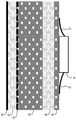
도 17은, 백플레인 지지대 층을 포함하는 후면-접촉/후면-접합 결정질 반도체 태양 전지의 단면도이다;
도 18은, 백플레인 층에 부착되고 백플레인 층 상에 고정된(mounted) 적어도 하나의 온-셀 전자 구성요소를 갖는 도 17에 나타낸 상기 전지와 유사한 후면-접합/후면-접합 결정질 반도체 태양 전지의 단면도이다;
도 19는, 태양 전지의 상기 백플레인 및 대표적인 집적된 백-접촉 (IBC) 금속화 패턴의 윗면(top view)을 나타내는 도표이다;
도 20은, 상기 에미터(emitter) 및 베이스 버스바(base busbars)에 상기 바이패스 스위치 리드의 높은 전도성 부착을 제공함으로써 핫 스팟을 최소화하고, 상기 전지의 후면 상에 상기 전지 말단 또는 버스바(busbar)에 직접적으로 부착된 바이패스 스위치를 갖는 도 19에서 상기 태양 전지의 상기 백플레인의 윗면을 나타내는 도표이다;
도 21은, 상기 백플레인 면 상의, 상기 에미터 및 베이스 버스바에서, 상기 전지 말단에 부착되고 상기 전지 말단 상에 직접적으로 고정된, DC-to-DC MPPT 전력 최적화기 또는 DC-to-AC MPPT 전력 최적화기를 갖는 도 19에서 상기 태양 전지의 상기 백플레인의 윗면을 나타내는 도표이다;
도 22는, 주어진 태양광 루미네이션 레벨(given sunlight illumination level)에서 수확한 최대 전력에 대한 최대 전력점(MPP) 및 태양 전지 Ⅳ 특성을 나타내는 그래프이다; 및
도 23은, 상이한 태양 모듈 일루미네이션 강도(different solar module illumination intensities) 하의, 작동의 피크 최대 전력점(peak maximum power points), 및 전력 vs 전압 특성을 나타내는 대표적인 태양 모듈을 위한 그래프이다. The nature, properties and advantages of the above-indicated subject matter may become more apparent from the detailed description set forth below when taken in conjunction with the drawings in which like reference numerals indicate like features:
Figures 1a and 1b are circuit diagrams illustrating equivalent circuit diagrams for solar PV cells;
FIG. 2A is a schematic diagram showing an equivalent circuit model of an ideal solar cell, FIG. 2B is a graph corresponding to the current-voltage (IV) characteristic of the solar cell under dark and sunlight illumination conditions to be;
Figures 3a and 3b are a plot of a typical 60-cell crystalline silicon solar module with one shaded and several partially shaded cells, respectively;
FIG. 4A is a chart showing the unshaded current path for the solar cell module serial connection, FIG. 4B shows the same solar cell module serial connection with the bypass diode and the shaded one module providing an alternative bypass current path It is a chart showing;
5 is a schematic diagram of an external bypass diode used in a module sub-string with the solar cell showing these equivalent circuit diagrams;
Figure 6 is a graph showing the current-voltage (IV) characteristics of a crystalline solar cell with a bypass diode and without a bypass diode;
Figure 7 is a chart showing an example of a crystalline silicon PV module having three shaded cells on different sub-strings of the series-connected solar cell;
Figures 8 and 9 are diagrams illustrating two examples of PV plant installations;
10 and 11 are diagrams illustrating examples of monolithic integration of a bypass diode (Schottky diode or pn junction diode) with a multi-junction compound semiconductor CPV cell;
Figure 12 is a process flow highlighting important processing steps in a thin-silicon, back-contact / back-junction crystalline silicon solar cell fabrication process;
Figure 13 is a schematic diagram showing a distributed cellular shade management system (a solar cell showing equivalent circuit diagrams thereof) of a distributed cell having one bypass diode per solar cell;
14 is a graph illustrating the IV characteristics of a metal-oxide-semiconductor field-effect transistor (MOSFET), which may be used as a bypass switch (or as part of a bypass switch circuit) It is a graph;
Fig. 15 is a schematic diagram of shade management execution of an ISIS distributed battery according to the above-mentioned subject matter (specifically, a circuit including a MOSFET or an embodiment using a MOSFET as a bypass switch);
FIG. 16 is a block diagram of an ISIS distributed cellular shade management solution according to the above-mentioned subject matter (an embodiment using a circuit comprising BJTs as a bipolar junction transistor-BJTs or a bypass switch clearly) )to be;
17 is a cross-sectional view of a back-contacting / back-bonded crystalline semiconductor solar cell comprising a backplane support layer;
Figure 18 is a cross-sectional view of a back-junction / back-junction crystalline semiconductor solar cell similar to the cell shown in Figure 17 with at least one on-cell electronic component attached to the backplane layer and mounted on the backplane layer. to be;
19 is a diagram showing the top view of the backplane and exemplary integrated back-contact (IBC) metallization pattern of a solar cell;
FIG. 20 is a cross-sectional view of a battery switch in accordance with an embodiment of the present invention, which minimizes hot spot by providing a high conductive attachment of the bypass switch lead to the emitter and base busbars, Figure 19 is a diagram showing the top surface of the backplane of the solar cell in Figure 19 with a bypass switch attached directly to the busbar;
Figure 21 is a cross-sectional view of a DC-to-DC MPPT power optimizer or DC-to-AC MPPT, which is attached to the battery end and is directly fixed on the battery end, at the emitter and base bus bar, FIG. 19 is a diagram showing the top surface of the backplane of the solar cell in FIG. 19 having a power optimizer; FIG.
22 is a graph showing the maximum power point (MPP) and solar cell IV characteristics for a maximum power harvested at a given sunlight illumination level; And
23 is a graph for a representative solar module showing peak peak power points of operation and power vs voltage characteristics under different solar module illumination intensities.
상세한 설명details
하기의 기재는 이로 제한하려는 의미가 아니고, 단지 본 내용의 일반적인 원리를 기재하는 목적으로 기재되어 있다. 본 내용의 범위는 상기 청구의 범위에 대한 참고로 결정되어야 한다. 본 내용의 대표적인 실시형태는, 다양한 도면의 이에 대응하는 부분을 나타내기 위해 사용된 유사한 번호로 도면에서 설명되어 있다.
The following description is not intended to be limiting, but merely for purposes of describing general principles of the present disclosure. The scope of the present disclosure should be determined by reference to the above claims. Exemplary embodiments of the present disclosure are illustrated in the drawings with like numerals used to indicate corresponding parts of the various figures.
그리고, 본 내용이 단결정질 실리콘 기판 및 그 밖의 기재된 제조 물질을 사용하여 특정한 후면 접촉 태양 전지와 같은, 특정한 실시형태와 관련하여 기재되었을지라도, 본 분야의 숙련자는, 전면 접촉 전지, 반도체 물질(갈륨 비소, 저마늄 등과 같은), 기술 영역, 및/또는 과도한 실험 없는 실시형태를 포함하는 그 밖의 물질에 본원에 기재된 원리를 적용할 수 있다.
Although the present disclosure has been described in connection with specific embodiments, such as specific rear-facing solar cells, using monocrystalline silicon substrates and other described manufacturing materials, those skilled in the art will appreciate that a front contact cell, a semiconductor material Arsenic, < / RTI > germanium, and the like), technical areas, and / or other materials, including those without undue experimentation.
상기에 나타내고 기재된 바와 같이, 공지된 결정질 실리콘(또는 다른 전지-기초된) PV 시스템에서, 최대 전력 추출 해결책 뿐만 아니라 그늘짐의 존재에서 신뢰할 만한 모듈 작동을 제공하는 핫 스팟 보호 및 현재의 최신의 태양 전지 보호는, 하나 또는 하기의 조합을 사용하는 것을 기초로 한다: 바이패스 다이오드, PV 모듈에서 직렬-연결된 태양 전지의 하나의 서브스트링 당 가장 일반적인 하나의 외부 바이패스 다이오드(일반적으로 세 개의 외부의 바이패스 다이오드는 결정질 실리콘 PV 모듈 당 외부의 모듈 접합 박스에 위치되어 있다); PV 모듈 당 외부의 하나 외부의 마이크로-인버터(또는 대체적으로 하나의 DC-to-DC 컨버터)를 사용하여 상기 모듈 레벨에서 최대 전력점 추적(MPPT); 및 상기 전지-기초된 PV 모듈의 상기 에너지 수득을 증가시키기 위해 상기 모듈 내의 상기 전지 사이에 프로그램화가능한 상호연결 기술(programmable interconnect technology).
In known crystalline silicon (or other cell-based) PV systems, as described and illustrated above, there is a maximum power extraction solution as well as hot spot protection that provides reliable module operation in the presence of shade, Battery protection is based on using one or a combination of the following: a bypass diode, the most common one external bypass diode per substring of a series-connected solar cell in a PV module (typically three external The bypass diode is located in an external module junction box per crystalline silicon PV module); Maximum power point tracking (MPPT) at the module level using one external external micro-inverter (or, generally, one DC-to-DC converter) per PV module; And a programmable interconnect technology between the cells in the module to increase the energy yield of the battery-based PV module.
바이패스 다이오드가 그늘진 전지를 보호할 수도 있고, 핫 스팟을 보호할 수도 있고, 핫 스팟으로 인한 모듈 고장 및 역방향 편향된 전지(reverse biased cells)를 예방할 수도 있으면서, 그들은 또한, 모듈 그늘짐 또는 솔링(soling)이 존재하는 경우에, 현실적인 필드 작동(realistic field operations)에서 모듈 전력 출력 손실로 인하여, 현저한 에너지 수득 감소를 결과적으로 야기한다. 예를 들어, 단일 그늘진 전지는, 상기 모듈 전력의 1/3의 손실을 결과적으로 야기할 수 있고(상기 바이패스 다이오드는 상기 그늘진 전지를 포함하는 전체의 20 개-전지 서브-스트링을 우회할 것이기 때문이다), 상기 단일 전지는, 표준 60 개-전지 모듈 디자인을 추정하는, 정상의 그늘지지 않은 조건 동안에 상기 모듈 전력의 1/60 만을 차지한다. 유사하게, 60 개-전지 PV 모듈에서 20 개-전지 서브-스트링 당 하나의 그늘진 전지를 추정하는, 세 개의 그늘진 전지(도 7에 나타낸 것과 같은 예) 와 함께, 모두 세 개의 바이패스 다이오드는 활성화되고, 상기 모듈로부터 추출된 전력은 제로(또는 100 % 손실의 모듈 전력)로 떨어지면서, 상기 세 개의 그늘진 전지는 정상의 비-그늘진 작동 조건 동안에 상기 모듈 전력의 오직 3/60(1/20)을 차지한다.
Bypass diodes can protect shaded cells, protect hot spots, prevent module failures due to hot spots and reverse biased cells, but they also prevent module shading or soling ), Resulting in a significant energy gain reduction, due to the module power output loss in realistic field operations. For example, a single shaded cell can result in a loss of one third of the module power (which bypass the entire 20-cell sub-string including the shaded cell, ), The single cell accounts for 1/60 of the module power during normal, non-shaded conditions, which presumes a standard 60-cell module design. Similarly, all three bypass diodes, with three shaded cells (an example as shown in Figure 7), which estimate 20 shaded cells per cell sub-string in a 60-cell PV module, , And the power extracted from the module drops to zero (or 100% loss of modular power), such that the three shaded cells exhibit only 3/60 (1/20) of the module power during normal non-shaded operating conditions, Respectively.
대조적으로, 본원에 기재된 해결책은, PV 설비 뿐만 아니라 그 밖의 관련된 이익을 위한 PV 모듈 전력 수확을 증가시키고, 에너지 수득을 증가시키기 위해, 예를 들어, 하기의 구성요소 또는 하기의 구성요소의 조합을 포함하는, 스마트 PV 전지 및 스마트 PV 모듈을 제공한다. 바이패스 스위치를 갖는 분포된 그늘 관리 해결책은, 각각의 태양 전지의 상기 후면 상에(예를 들어 상기 전지 백플레인 상에) 고정되고, 상기 후면 상으로 집적되고, 상기 모듈 조립체 내에 라미네이트 되고/끼워지고(A distributed shade management solution having a bypass switch mounted onto and integrated on the backside of each solar cell and laminated/embedded within the module assembly)-따라서, 외부의 바이패스 다이오드를 갖는 상기 외부의 접합 박스를 위한 필요가 제거되었고, 전체적인 모듈 신뢰성이 증가하였다. 분포된 전력 최적화기 및 에너지 수득 개선 해결책은,각각의 태양 전지 후면 상 내로(예를 들어 상기 전지 백플레인 상에) 하나의 DC-to-DC 컨버터 전력 최적화기 또는 하나의 DC-to-AC 마이크로-인버터 전력 최적화기를 포함한다. 상기 전지-레벨 전력 최적화기 전자장치[예를 들어, 모놀리식 단일-칩 해결책(monolithic single-chip solution)]은, 상기 후면-접촉 태양 전지의 상기 후면 백플레인 상에 포함되고 상기 후면 백플레인 상에 고정될 수도 있고, 상기 모듈 조립체 내로 라미네이트 되고/끼워진다. 상기 나타낸 다양한 전력 최적화기 실시형태에서, 각각의 전지로부터 추출된 전력은, 그늘짐 조건 및 수득된 분포된 그늘 관리 해결책에도 불구하고 최대화될 수도 있다.
In contrast, the solution described herein can be used, for example, in combination with the following components or combinations of the following components to increase the PV module power harvest and increase energy yield for PV equipment as well as other related benefits , A smart PV cell and a smart PV module. A distributed shade management solution with a bypass switch is fixed (e.g., on the battery backplane) on the back surface of each solar cell, integrated onto the back surface, laminated / sandwiched within the module assembly Thus, there is no need for an external junction box with an external bypass diode to be eliminated. ≪ RTI ID = 0.0 > [0006] < / RTI & And the overall module reliability has increased. The distributed power optimizer and the energy gain improvement solution can be implemented in a single DC-to-DC converter power optimizer or one DC-to-AC micro-power optimizer (e.g., on the battery backplane) Inverter power optimizer. The battery-level power optimizer electronics (e.g., a monolithic single-chip solution) is included on the back-side backplane of the back-contacting solar cell and the back- And may be fixed and laminated / fitted into the module assembly. In the various power optimizer embodiments shown above, the power extracted from each cell may be maximized despite the shade conditions and the distributed shade management solutions obtained.
상기 나타낸 시스템 및 방법은, 매우-낮은-비용 분포된 전지-레벨 (전지의) 전력 전자장치를 포함하고, 시스템 비용(설치된 < $ 1/W의 설치된 시스템을 가능하게 함)을 감소하고, 에너지 수득의 면에서 수행을 증가시키는 능력(< $ 0.05 - $ 0.10/kWh Levelized Cost of Electricity 또는 LCOE을 가능하게 함)을 갖는 스마트 PV 전지 및 스마트 PV 모듈을 제공한다. 비용 및 효율은 태양 전지 제조에서의 중요한 역할을 하고, 상기에 나타낸 바와 같이, 결정질 실리콘 광발전(PV) 모듈은 현재전체의 세계적인 PV 마켓의 85 % 이상을 차지한다. 현재, 시작하는 실리콘 웨이퍼 비용은, 상기 결정질 실리콘 PV 모듈 제조 비용의 대략 40 %를 차지한다.
The system and method described above includes a very low-cost distributed battery-level (of a battery) power electronics and reduces the system cost (enabling an installed system installed <$ 1 / W) Smart PV modules and smart PV modules with the ability to increase performance in terms of yield (<$ 0.05 - $ 0.10 / kWh enabling Leveled Cost of Electricity or LCOE). Cost and efficiency play an important role in solar cell manufacturing, and as shown above, crystalline silicon photovoltaic (PV) modules currently account for more than 85% of the entire global PV market. Currently, the starting silicon wafer cost accounts for approximately 40% of the cost of manufacturing the crystalline silicon PV module.
도 12는, 다공성 실리콘의 방출 층 상의 재사용가능한 템플레이트 및 에피택셜 실리콘 증착을 사용하여, 스마트 전지 및 스마트 모듈을 위한, 라미네이트된 백플레인을 갖는 저-비용, 높은-효율, 후면-접합/후면-접촉 단결정질 전지를 만들기 위해, 통상적인 제조 공정을 제거하고, 실리콘 사용을 실질적으로 감소하는, 얇은-결정질-실리콘 태양 전지 제조 공정의 중요한 프로세싱 단계를 강조한 공정 흐름도이다. 상기 스마트 전지는 적어도 하나 또는 전자 구성요소(상기 백플레인 상에 부착되고 상기 백플레인 상에 직접적으로 고정된 바이패스 스위치 및/또는 DC-to-DC 또는 DC-to AC MPPT 전력 최적화기와 같은)의 조합을 포함한다.
12 is a low-cost, high-efficiency, back-bonding / back-contact having a laminated backplane for smart cells and smart modules, using reusable templates and epitaxial silicon deposition on a porous silicon release layer. Is a process flow diagram highlighting important processing steps in a thin-crystalline-silicon solar cell fabrication process, removing conventional fabrication processes and substantially reducing silicon usage, to make monocrystalline cells. The smart cell may comprise at least one or a combination of electronic components (such as bypass switches and / or DC-to-DC or DC-to-AC MPPT power optimizers mounted on the backplane and directly fixed on the backplane) .
상기 공정은 다공성 실리콘의 얇은 희생층(thin sacrificial layer)이 형성(예를 들어, 전기 회로의 존재에서 HF/IPA 습윤 화학에서 표면 변형 공정을 통해 전기화학적인 에칭 공정에 의해)된 내로 재사용가능한 실리콘 템플레이트(p-타입 단결정질 실리콘 웨이퍼로 일반적으로 제조됨)와 함께 시작한다. 높은-품질의 에피택셜 시드 층 뿐만 아니라 차후의 분리/리프트-오프 층(subsequent separation/lift-off layer) 둘 다로서 제공하는 상기 희생적 다공성 실리콘 층을 형성하자마자, 윈 위치-도핑된 단결정질 실리콘(in-situ-doped monocrystalline silicon)의 얇은 (일반적으로 몇몇 미크론에서 약 70 미크론까지의 범위, 가장 바람직하게 약 50 미크론의 두께를 가짐) 층이 형성되고[예를 들어, 트리클로로실란 또는 TCS 및 수소와 같은 실리콘 가스를 포함하는 주위에서(in ambient) 화학적-증기 증착 또는 CVD 공정을 사용하는 대기의-압력 에피택시(atmospheric-pressure epitaxy)], 에피택셜 성장이라고 또한 불린다. 전지 프로세싱 단계의 대다수의 완성 후에, 매우-낮은 비용 백플레인 층은, 상기 태양 전지의 높은-전도성 전지 금속화를 지지할 뿐만 아니라 영구 전지 지지대 및 강화(permanent cell support and reinforcement)를 위한 상기 얇은 epi 층에 결합된다. 일반적으로, 상기 백플레인 물질은, 상기 공정의 집적화 및 신뢰성의 필요를 충족하는, 비용이 비싸지 않은 프리프레그 물질(inexpensive prepreg material)(흔히, 프린트된 회로 보드에서 사용됨)과 같은 얇은(예를 들어 약 50 내지 250 미크론), 유연한, 전기적으로 설비하는 중합체 물질 시트(electrically insulating polymeric material sheet)로 이루어져 있다. 대부분-공정된 후면-접촉, 후면-접합 백플레인-강화된 큰-영역(예를 들어, 적어도 125 mm x 125 mm 및 더 큰 태양 전지 영역을 갖는) 태양 전지는 그리고 난 다음에 분리되고, 기계적으로-약화된 희생적인 다공성 실리콘 층(예를 들어, 기계적인 방출 MR 공정을 통해)을 따라 상기 템플레이트로부터 들어올려지면서, 상기 템플레이트는 여러 번 재-사용될 수도 있고, 이로 인하여 상기 태양 전지 전지 제조 비용을 추가적으로 최소화된다. 그리고 난 다음의 최종의 전지 프로세싱은, 템플레이트로부터 방출된 후에 노출된 서니-사이드 상에서 수행될 수도 있다[예를 들어, 상기 전면 텍스처(frontside texture) 및 패시베이션(passivation) & 무-반사 코팅 증착 공정(anti-reflection coating deposition process)을 완성함으로써].
The process may be carried out using a thin sacrificial layer of porous silicon formed (e.g., by electrochemical etching through a surface modification process in HF / IPA wet chemistry in the presence of an electrical circuit) into a reusable silicon Template (generally made of p-type monocrystalline silicon wafer). As soon as the sacrificial porous silicon layer provided as both a high-quality epitaxial seed layer as well as a subsequent separation / lift-off layer is formed, the win position-doped monocrystalline silicon ( (typically having a thickness in the range of from several microns to about 70 microns, most preferably about 50 microns) of in-situ-doped monocrystalline silicon (for example, trichlorosilane or TCS and hydrogen Atmospheric-pressure epitaxy using an in-ambient chemical vapor deposition or CVD process involving a silicon gas such as, for example, silicon gas. After the completion of the majority of the battery processing steps, the very-low cost backplane layer not only supports the high-conductivity battery metallization of the solar cell, but also the thin epi layer for permanent cell support and reinforcement Lt; / RTI > Generally, the backplane material is made of a thin (e.g., about < RTI ID = 0.0 > a < / RTI > drug) material such as an inexpensive prepreg material (often used in printed circuit boards) that meets the need for integration and reliability of the process. 50 to 250 microns), and a flexible, electrically-conductive polymeric material sheet. (For example, with a solar cell area of at least 125 mm x 125 mm and a larger solar cell area) is then separated and mechanically separated from the back-contact back- The template may be re-used multiple times, lifted from the template along with a sacrificial sacrificial porous silicon layer (e.g., via a mechanical emissive MR process), thereby reducing the cost of manufacturing the solar cell battery Additionally, it is minimized. The final cell processing then may be performed on the exposed sunny side after being emitted from the template (e.g., the frontside texture and passivation & anti-reflection coating deposition process anti-reflection coating deposition process].
백플레인-끼워진 상호연결(backplane-embedded interconnect) 및 강화 백플레인과 함께 후면-접합/후면-접촉 전지 디자인의 조합은, 표면 실장 기술(surface mount technology, SMT)과 같은 안정된 전기장치 조립체 방법을 사용하여 상기 전지 레벨에서 매우-낮은-비용 전력 전자장치의 신뢰가능한 집적화를 위한 권능을 부여하는 전지 구성(enabling cell architecture)을 제공한다. 높은-효율성 얇은 결정질 실리콘 태양 전지를 위한 끼워진 높은-전도성(알루미늄 및/또는 구리) 상호연결을 제공하고, 영구적인 구조적인 지지대/강화로서 역할에 추가적으로, 이러한 백플레인 기술은, 증명된 후면-접촉 모듈 조립체 및 루미네이션 기술과 함께 호환성을 유지하면서, 상기 전지의 서니사이드와 함께 간섭없이 상기 전지 백플레인 상에, 바이패스 스위치 및 MPPT 전력 최적화기와 같은, 매우-저-비용 전력 전자 구성요소의 접적화를 가능하게 한다[즉, 어떠한 활성 일루미네이션 영역이 상기 전지의 후면의 백플레인 상에 고정된 상기 전지-기초된 전자장치에 의해 소비되지 않기 때문에, 어떠한 효율성 패널티(efficiency penalty)도 없다].
The combination of a backplane-embedded interconnect and a back-junction / back-contact battery design with a reinforced backplane is accomplished using a stable electrical device assembly method, such as surface mount technology (SMT) Provides an enabling cell architecture that provides power for reliable integration of very-low-cost power electronic devices at the battery level. In addition to providing a built-in high-conductivity (aluminum and / or copper) interconnect for high-efficiency thin crystalline silicon solar cells and serving as a permanent structural support / reinforcement, this backplane technology is a proven back- Low-cost power electronic components, such as a bypass switch and an MPPT power optimizer, on the battery backplane without interfering with the sunside of the battery while maintaining compatibility with the assembly and the luminous technology (That is, there is no efficiency penalty because no active illumination area is consumed by the battery-based electronic device fixed on the backplane of the back of the cell).
상기 백플레인 물질은 바람직하게, 상기 얇은 실리콘 층 상의 과도한 열적으로 유도된 스트레스(excessive thermally induced stresses)를 유발하지 않는, 충분하게 낮은 계수의 열 팽창(low coefficient of thermal expansion, low CTE)과 함께 중합체 물질의 얇은 시트일 수도 있다. 게다가, 상기 백플레인 물질은, 상기 말미 전지 제조 공정 동안에 상기 공정 집적화 필요성, 특히, 상기 전면 패시베이션 및 ARC 층의 상기 PECVD 증착 동안에 상기 전지 전면 및 열 안정성의 습식 텍스쳐링(wet texturing) 동안에 화학적인 저항을 충족하여야 한다. 게다가, 상기 전기 절연 백플레인 물질은 상기 모듈-레벨 라미네이션 공정 및 장기간 신뢰성 필요성을 충족하여야 하면서, 다양한 안정된 중합체[플라스틱, 플루오로중합체, 프리프레그(prepregs) 등과 같은] 및 비-중합체 물질(유리, 세라믹 등과 같은)은, 상기 백플레인 물질로서 고려되고, 가능한 사용될 수도 있고, 상기 최적의 선택은, 비용, 공정 집적화의 용이함, 신뢰성, 유연성 등을 포함하지만 이로 제한되지 않는 많은 고려사항에 따라 달라진다. 상기 프리프레그 시트는 프린트된 회로 보드의 빌딩 블록(building block)으로서 사용된다. 프리프레그 시트는 레진 및 CTE-감소하는 섬유 또는 입자의 조합으로부터 제조된다. 바람직하게, 상기 백플레인 물질은, 텍스쳐 화학(texture chemistry)에서 상대적으로 화학적으로 저항력이 있고, 적어도 180 ℃ 까지, 및 보다 바람직하게 적어도 약 280 ℃까지의 온도에서 열적으로 안정되는, 비싸지 않고, 낮은-CTE(일반적으로 CTE <10 ppm/℃ 및 보다 바람직하게 CTE <5 ppm/℃), 얇은 (일반적으로 50 내지 250 미크론, 바람직하게 50 내지 100 미크론) 프리프레그 시트일 수도 있다. 상기 프리프레그 시트는, 진공 라미네이터(vacuum laminator)를 사용하여, 상기 태양 전지 후면에 일반적으로 부착되면서, 여전히 상기 템플레이트 상에서 있다(상기 전지 리프트 오프 공정 전에). 열 및 압력을 적용하면서, 상기 얇은 프리프레그 시트는 영구적으로(permanently), 상기 공정된 태양 전지의 상기 후면에 부착되거나 또는 라미네이트된다. 그리고 난 다음에, 상기 리프트-오프 방출 경계선(lift-off release boundary)은, 펄스 레이저 스크리빙 도구(pulsed laser scribing tool)를 일반적으로 사용하는, 상기 태양 전지의 주변(상기 템플레이트 가장자리에 가까움) 주의에 정의되고, 그리고 난 다음에, 상기 백플레인-라미네이트된 태양 전지는, 기계적인 방출 또는 리프트-오프 공정(lift-off process)을 사용하여 상기 재사용가능한 템플레이트로부터 분리된다. 차후의 공정 단계는 하기를 포함할 수도 있다: (ⅰ) 상기 태양 전지 서니사이드 상의 상기 텍스쳐 및 패시베이션 공정의 완성(completion), (ⅱ) (상기 태양 전지의 백플레인인) 상기 전지 후면 상의 상기 태양 전지 높은 전도성 금속화의 완료. 상기 높은-전도성 금속화(상기 태양 전지 제조 및 물질 비용을 감소하기 위해, 일반적으로 알루미늄 및/또는 구리를 포함하지만, 바람직하게 은을 포함하지 않음)는, 상기 태양 전지의 백플레인 상에 형성되고, 상기 에미터(emitter) 및 베이스 양극성(base polarities) 둘 다를 포함한다.
The backplane material preferably has a sufficiently low coefficient of thermal expansion (CTE) that does not cause excessive thermally induced stresses on the thin silicon layer, Lt; / RTI > In addition, the backplane material meets chemical resistance during the end cell manufacturing process during the process integration, especially during wet texturing of the cell front and thermal stability during the PECVD deposition of the front passivation and ARC layers. shall. In addition, the electrically insulated backplane material must be able to meet a variety of stable polymers (such as plastics, fluoropolymers, prepregs, etc.) and non-polymeric materials (glass, ceramics, Etc.) may be considered and possibly used as the backplane material, and the optimal choice will depend on many considerations including, but not limited to, cost, ease of process integration, reliability, flexibility, and the like. The prepreg sheet is used as a building block of a printed circuit board. The prepreg sheet is made from a combination of resin and CTE-reducing fibers or particles. Preferably, the backplane material is relatively inexpensive, chemically resistant in texture chemistry, and is thermally stable at temperatures up to at least 180 ° C, and more preferably at least up to about 280 ° C. (Typically 50 to 250 microns, preferably 50 to 100 microns) of prepreg sheet, preferably a CTE (generally CTE <10 ppm / ° C and more preferably a CTE <5 ppm / The prepreg sheet is still on the template (prior to the battery lift-off process), generally attached to the back of the solar cell, using a vacuum laminator. Applying heat and pressure, the thin prepreg sheet is permanently attached to, or laminated to, the backside of the processed solar cell. The lift-off release boundary is then used to position the periphery of the solar cell (near the edge of the template), which typically uses a pulsed laser scribing tool, , And then the backplane-laminated solar cell is separated from the reusable template using a mechanical release or lift-off process. Subsequent processing steps may include: (i) completion of the texture and passivation process on the solar cell sunside, (ii) completion of the texture and passivation process on the solar cell backside of the solar cell backplane (which is the backplane of the solar cell) Completion of high conductivity metallization. The high-conductivity metallization, generally comprising aluminum and / or copper, but preferably not including silver, to reduce the solar cell fabrication and material cost, is formed on the backplane of the solar cell, And includes both the emitter and base polarities.
예를 들어, 본원에 기재된 바와 같은 상기 태양 전지 디자인 및 제조 공정은, 상기 전기적으로 절연처리된 백플레인 층에 의해 분리되는 두 레벨의 금속화를 갖는다. 상기 백플레인 라미네이션 공정 전에, 상기 후면-접촉 태양 전지 상에 근본적인 마지막 공정은, 바람직하게 스크린 프린트된 또는 플라즈마 스퍼터링된 (PVD) 알루미늄(또는 알루미늄 실리콘 합금) 물질 층의 얇은 층을 사용하여, 상기 전지 후면 상에 직접적으로 상기 태양 전지 베이스 및 에미터 접촉 금속화 패턴을 형성하기 위한 것이다. 금속화의 이러한 첫 번째 층(M1)은, 상기 IBC 전지의 상기 베이스 및 에미터 영역을 정의하는, 최적-피치 집적된 후면-접촉(IBC) 전도체 핑거(fine-pitch interdigitated back-contact conductor fingers)와 같은, 상기 태양 전지 접촉 금속화 패턴을 정의한다. 상기 M1 층은, 금속의 이러한 첫 번째 층 후에 형성될 것인, 상기 태양 전지 전기적인 전력을 제2 레벨의 보다 높은-전도성 태양 전지 금속화(M2 층)으로 이송하기 위해, 상기 태양 전지 전류 및 전압을 추출하기 위해 제공된다. 상기 라미네이트된 백플레인의 형성, 상기 템플레이트로부터 상기 백플레인-지지된 태양 전지의 그 다음의 부착, 및 상기 전면 텍스쳐 및 패시베이션 공정의 완성 후에, 상기 남아있는 공정은, 상기 백플레인 상의 보다 높은 전도성 M2 층을 형성하기 위한 것이다. 많은 수(일반적으로 100's 내지 1000's)의 비아 홀(via hole)은, 상기 백플레인 내로 구멍을 뚫는다[바람직하게 레이저 드릴링(laser drilling)을 사용함]. 이러한 비아 홀은, 이러한 비아 홀에서 형성된 전도성 플러그(conductive plugs)를 통해 상기 패턴된 M2 및 M1 층 사이의 차후의 전기적인 연결을 위한 M1의 예비-명시된 영역(pre-specified regions) 상에 이른다(land). 그 뒤에, 상기 패턴된 보다 높은-전도성 금속화 층 M2 가 형성된다[알루미늄 및/또는 구리를 포함하는 M2를 갖는- 플라즈마 스퍼터링(plasma sputtering) 및 도금(plating)의 하나 또는 조합에 의해]. 최적-피치(예를 들어, 100's의 핑거(M1 상의 IBC 핑거))를 갖는 집적된 후면-접촉 (IBC) 태양 전지를 위해, 상기 패턴된 M2 층은 M1에 직각인 것으로 바람직하게 디자인되어 있고, 즉, 상기 M2 핑거는 M1 핑거에 필수적으로 직각이다. 게다가, 이러한 직각의 변형 때문에, 상기 M2 층은 상기 M1 층보다 보다 낮은 IBC 핑거를 갖는다[예를 들어, 약 10 내지 50이 못되는 M2 핑거의 인자(factor)에 의해]. 이런 이유로, 상기 M2 층은, 상기 M1 층보다 보다 더 넓은 IBC 핑거를 갖는 보다 간격이 넓은 패턴이다(the M2 layer is a much coarser pattern with much wider IBC fingers than the M1 layer). 이러한 실시형태에서, 상기 태양 전지 버스바는, 전지 상의 상기 버스바와 연관된 상기 전기적인 그늘짐 손실(electrical shading losses)을 제거하기 위해, 상기 M2 층 상에 설치된다(및 상기 M1 상에는 설치되지 않음). 상기 베이스 및 에미터 상호연결 및 버스바 둘 다가 상기 태양 전지 후면 백플레인 상의 상기 M2 층 상에 이용가능하게 제조되기 때문에, 이러한 본 발명의 상기 실시형태는, 상기 백플레인 상의 상기 태양 전지의 상기 베이스 및 에미터 말단 둘 다에 접근과 함께 상기 백플레인 상의 상기 전력 전기장치 구성요소 또는 구성요소들을 효과적으로 집적화할 수 있다.
For example, the solar cell design and fabrication process as described herein has two levels of metallization separated by the electrically insulated backplane layer. Prior to the backplane lamination process, a fundamental last step on the back-contacting solar cell is to use a thin layer of a layer of preferably screen printed or plasma sputtered (PVD) aluminum (or aluminum silicon alloy) material, To form the solar cell base and emitter contact metallization pattern directly on the substrate. This first layer (M1) of metallization has an optimized-pitch interdigitated back-contact conductor fingers (IBC) defining the base and emitter regions of the IBC cell. Lt; RTI ID = 0.0 > metallization < / RTI > The M1 layer may be formed to transport the solar cell electrical power to a second level of higher-conductivity solar cell metallization (M2 layer), which will be formed after this first layer of metal, And is provided for extracting the voltage. After the formation of the laminated backplane, the subsequent attachment of the backplane-supported solar cell from the template, and the completion of the frontal texturing and passivation process, the remaining process forms a higher conductive M2 layer on the backplane . A large number of (typically 100's to 1000's) via holes puncture the backplane (preferably using laser drilling). These via holes are over the pre-specified regions of M1 for subsequent electrical connection between the patterned M2 and M1 layers through conductive plugs formed in such via holes ( land). Thereafter, the patterned higher-conductive metallization layer M2 is formed (by one or a combination of plasma sputtering and plating with M2 comprising aluminum and / or copper). For an integrated back-contact (IBC) solar cell having an optimum pitch (e.g., 100's of fingers (IBC finger on M1)), the patterned M2 layer is preferably designed to be perpendicular to M1, That is, the M2 finger is essentially perpendicular to the M1 finger. In addition, due to this orthogonal transformation, the M2 layer has a lower IBC finger than the M1 layer (e.g., by a factor of M2 finger less than about 10 to 50). For this reason, the M2 layer, the gap is wider than the pattern with a wider finger more than IBC layer M1 (t he layer M2 is a much coarser pattern with much wider than the fingers IBC M1 layer). In this embodiment, the solar cell bus bar is installed on the M2 layer (and not on the M1) to eliminate the electrical shading losses associated with the bus bar on the cell. . Since both the base and emitter interconnections and the bus bar are made available on the M2 layer on the solar cell backplane, this embodiment of the present invention is characterized in that the base of the solar cell on the backplane and the emitter The power electronics components or components on the backplane can be effectively integrated with access to both terminals.
매우 낮은-비용 프린트된-회로 보드와 본질적으로 유사하게, 상기 백플레인 상의 상기 태양 전지의 양극성 둘 다를 갖는 상기 나타낸 태양 전지 백플레인은, 상기 태양 전지의 서니사이드를 방해함이 없고, 상기 태양 전지의 신뢰성의 소멸없이 상기 전지의 후면 백플레인 상에 전자 구성요소를 전기적으로 조립하고, 집적화하는데 효과적으로 사용될 수도 있고, 이런 이유로 상기 전체적인 전지 및 모듈을 통해 보다 스마트한 전력 관리를 통해 개선된 에너지 수득, 분포된 전지-기초된 MPPT 전력 최적화, 감소된 LCOE, 및 개선된 PV 시스템 및 신뢰성을 갖는 분리된 그늘 관리의 실행을 가능하게 한다. 상기 백플레인은, 상기 태양 전지 상의 얇은-형식의 전자 구성요소의 직접적인 고정, 부착 및 지지를 가능하게 할 뿐만 아니라, 이는 또한 상기 구성요소 및 이들의 부착의 어떠한 해로운 스트레스 효과(any detrimental stress effects)를 상기 민감성 태양 전지(sensitive solar cell)로부터 효과적으로 분리한다. 본원에 기재된 상기 실시형태는, 영구적으로 부착된(즉, 라미네이트된) 백플레인을 갖는, 후면-접촉/후면-연결 IBC 전지를 포함하는 후면-접촉 태양 전지와 같은, 스마트 태양 전지 및 스마트 태양 모듈을 가능하게 한다. 상기 스마트 전지는, 각각의 전지 상에 상기 백플레인 내로 직접적으로 부착된 상기 전지 백플레인 및/또는 하나의 DC-to-DC or DC-to AC MPPT 전력 최적화기 상에 집적된 하나의 바이패스 스위치와 같은 전자 구성요소를 포함한다.
The solar cell backplane shown, having essentially both the polarity of the solar cell on the backplane, essentially similar to a very low-cost printed-circuit board, does not interfere with the sunny side of the solar cell, Can be effectively used to electrically assemble and integrate electronic components on the back-side backplane of the battery without dissipation of power from the battery. For this reason, improved energy yields through smarter power management through the overall battery and module, - Enables the implementation of the underlying MPPT power optimization, reduced LCOE, and separate shade management with improved PV system and reliability. The backplane not only allows direct fixation, attachment and support of thin-type electronic components on the solar cell, but it also allows for any detrimental stress effects of the components and their attachment And effectively isolates it from the sensitive solar cell. The embodiments described herein relate to a smart solar cell and smart solar module, such as a back-contacting solar cell comprising a back-contact / back-connecting IBC cell having a permanently attached (i.e., laminated) . The smart battery may be a single bypass switch integrated on the battery backplane and / or one DC-to-DC or DC-to-AC MPPT power optimizer directly attached to the backplane on each battery Electronic components.
지능적인 전지의 그늘 영향 억제( Intelligent cellular Shade Impact Suppression , ISIS) . PV 시스템의 직렬연결(series wiring)로 인하여, 시스템의 빛-흡수 표면 상의 작은 양의 차단은, 많은 산출량 손실(output loss)을 유도할 수도 있다. 전지 및 모듈의 그늘짐의 결과로서 전력 수확 능력의 손실의 다양한 대표적인 예가 있다. 예를 들어, 하나의 공개된 연구는, 상기 PV 모듈 표면 영역의 0.15%, 2.6%, 및 11.1% 상의 차단이 각각 3.7%, 16.7%, 및 36.5%의 산출량 전력 손실을 유발하고, 이런 이유로 그늘짐의 경우에 상기 설치된 PV 시스템 에너지 수득의 현저한 감소를 결과적으로 야기됨을 관찰하였다. 상기에 기재된 바와 같이, 그늘짐으로 인한 하나의 차단된 전지의 전류가 떨어진 경우에, 상기 그늘진 전지는, 스트링 또는 서브-스티링(sub-string)에서 직렬연결로 연결된 모든 다른 전지의 전류를 끌어내린다(시정 조치가 상기 모듈의 설계에서 취해질지라도). 상기 나타낸 주제의 신규한 ISIS 또는 그늘 관리 설계는, 상기 PV 모듈 및 상기 직렬연결 스트링 상의 최소한의 영향과 함께 어떠한 차단된 및 그늘진 전지 주위의 전기의 자동적인 재-경로변경(automatic re-routing)을 가능하게 하도록, 상기 태양 전지의 버스바(베이스 및 에미터) 둘 다에 직접적인 접근 및 전기적인 연결과 함께 각각의 태양 전지 상의 비용이 비싸지 않는 전기장치[예를 들어, 전력 쇼트키 다이오드 또는 MOSFET 또는 또 다른 적합한 낮은-정방향-전압/낮은-역방향-누출/낮은-ON-저항(low-forward-voltage/low-reverse-leakage/low-ON-resistance) 바이패스 스위치와 같은 매우 낮은-비용 전력 전자장치 바이패스 스위치]를 집적화한다-그렇게 함으로써 상기 PV 모듈의 전력 수확 및 전체적인 에너지 수득 산출량을 최대화한다. 추가적으로, 본원에 나타낸 상기 나타낸 ISIS 시스템 및 방법은, 상기 모듈 내에 어울리지 않는 전력과 관련된 축적된 열로부터의 스트레스를 감소시킴으로써 상기 전체적인 전지 및 모듈 신뢰성을 향상할 수도 있다. 본원에 나타낸 바와 같은 집적된 ISIS는, 외부의 바이패스 다이오드를 갖는 연결 박스를 위한 필요성을 제거하고, 이런 이유로 상기 결과적으로 형성된 스마트 모듈의 상기 비용/Wp를 감소한다. 추가적으로, 상기 전기 구성요소를 위한 지지 기판으로서 사용된 백플레인은 효과적으로 분리되고, 구성요소 배치 및 상기 민감성 반도체 전지로부터의 납땜의 상기 스트레스 효과를 효과적으로 분리하고, 따라서, 상기 전지 백플레인 및 후면 상의 상기 ISIS 바이패스 스위치를 고정하는 것과 관련된 이러한 스트레스의 어떠한 해로운 효과 및 열적 및 기계적인 스트레스를 최소화한다(Further, backplanes used as support substrates for the electronic components effectively isolate and decouple the stress effects of component placements and soldering from the sensitive semiconductor cell layers thus minimizing thermal and mechanical stresses and any detrimental effects of such stresses associated with mounting the ISIS bypass switches on cell backplanes and backsides).
The shade effect of suppressing intelligence cell (Intelligent cellular Shade Impact Suppression , ISIS) . Due to the series wiring of the PV system, a small amount of blocking on the light-absorbing surface of the system may lead to a large output loss. There are various representative examples of loss of power harvesting ability as a result of shading of the battery and the module. For example, one published study found that blocking above 0.15%, 2.6%, and 11.1% of the surface area of the PV module resulted in output power losses of 3.7%, 16.7%, and 36.5%, respectively, Resulting in a significant reduction of the installed PV system energy gain in the case of load. As described above, in the event that the current of one disconnected cell due to shading drops, the shaded cell draws current from all other cells connected in series connection in a string or sub-string (Even if corrective action is taken in the design of the module). The novel ISIS or shade management design of the above-indicated subject provides automatic re-routing of electricity around any blocked and shaded cells with minimal impact on the PV module and the series connected strings (E. G., A power Schottky diode or a MOSFET or a < RTI ID = 0.0 > MOSFET < / RTI > Another very low-cost power electronics such as a suitable low-forward-voltage / low-reverse-leakage / low-ON-resistance bypass switch Device Bypass Switch] - thereby maximizing the power harvest and overall energy yield of the PV module. Additionally, the above-indicated ISIS systems and methods shown herein may improve overall battery and module reliability by reducing stress from accumulated heat associated with unacceptable power within the module. An integrated ISIS as shown herein eliminates the need for a connection box with an external bypass diode and for this reason reduces the cost / Wp of the resulting smart module. In addition, the backplane used as a support substrate for the electrical component is effectively separated, effectively isolating the component placement and the stress effect of soldering from the sensitive semiconductor cell, and thus effectively isolating the ISIS bi- Pass switches and minimizes thermal and mechanical stresses associated therewith associated with fixing the pass switches (Further, backplanes are used as support components for effectively isolating and decoupling the stresses from component locations and soldering from the sensitive semiconductor cell layers thus minimizing thermal and mechanical stresses and any detrimental effects of such stresses associated with mounting the ISIS bypass switches on cell backplanes and backsides.
분포된 최대- 전력점 추적 최적화기( Distributed Maximum - Power - Point Tracking ( MPPT ) Power Optimizer ). 상기 최대 전력점(MPP)는, 모듈이 동틀녁에서 해질녁까지[또는 상기 태양 전지가 동틀녁에 "작동하는(wakes up)" 경우에서 출발하여, 상기 전지가 해질녁에 "정지(sleeps)"할 때까지]의 다양한 태양 일루미네이션 하의 최대 가능한 산출량 전력을 수득한 경우에 상기 전력-전압 연속체(current-voltage continuum) 상의 지점이다. 전류 및 전압 수치는 하루 동안에 상기 전지 조사 흐름 변화 및 그 밖의 작동 조건(주위 온도 등과 같은)에 따라 다양한 것과 같이, 자동화된 MPP 추적자(automated MPP tracker)는, 상기 MPP 조건에서 작동하도록(상기 최대 모듈 전력을 추출하기 위해), 상기 IV 곡선 상의 전압 및 전류의 작동점을 조절한다; 게다가, 상기 MPP 추적자는 또한, 직렬 연결된 상기 태양 전지(및 모듈) 모두의 상기 전류 수치를 일치하기 위해, 이의 산출량 전류/전압 비율을 바람직하게 조절한다. 상기 나타낸 혁신은, 상기 백플레인을 통해 각각의 전지 후면 위로 스마트 전자장치를 집적화함으로써 상기 전지 레벨에서 매우-낮은-비용 최대 전력점 추적 (MPPT) 전력 최적화 회로의 정확히 분포된 실행을 제공한다. 만약 하나의 외부의 마이크로-인버터(또는 대체적으로, 하나의 DC-to-DC 컨버터)를 사용하여 모듈 및 모듈-레벨 MPPT 당 하나의 외부의 마이크로-인버터(또는 대체적으로, 하나의 DC-to-DC 컨버터)가 사용된다면, 이러한 배열은, 상기 제1 스트링로부터 100 % 및, 예를 들어 상기 제2 스트링으로부터 97 %의 전력을 생산할 수도 있다. 이는, 상기 통상적인 중앙화된 인버터 MPPT 배열과 비교된 실질적인 개선, 상기 PV 설비로부터 완전한 전력의 98.5 %의 개선된 전력 수확을 수득할 것이다.
The distribution of the maximum-power point tracking Optimizer (Distributed Maximum - Power - Point Tracking ( MPPT ) Power Optimizer ). The maximum power point (MPP) is determined by the module starting from the cross country to the deadline (or in the event that the solar cell "wakes up" in the evening), so that the battery "sleeps" Is a point on the current-voltage continuum when the maximum possible output power under various solar illuminations of the current-voltage continuum is obtained. An automated MPP tracker may be configured to operate in the MPP conditions such that the current and voltage values vary with the cell irradiation flow change and other operating conditions (such as ambient temperature, etc.) during the day, To extract power), to adjust the operating point of the voltage and current on the IV curve; In addition, the MPP tracer also preferably adjusts its output current / voltage ratio to match the current values of all the solar cells (and modules) in series connection. The innovation shown above provides a well-distributed implementation of a very-low-cost maximum power point tracking (MPPT) power optimization circuit at the battery level by integrating smart electronics over the back of each battery via the backplane. If one external micro-inverter (or, alternatively, one DC-to-DC converter) is used per module and module-level MPPT using one external micro-inverter (or, alternatively, one DC- DC converter) is used, this arrangement may produce 100% from the first string and 97% from the second string, for example. This will result in a substantial improvement compared to the conventional centralized inverter MPPT arrangement, an improved power harvest of 98.5% of full power from the PV plant.
본원에 나타낸 바와 같은 상기 전지-레벨 MPPT 전력 최적화에 연장되고 적용된 경우에, 이러한 해결책은, 다양한 일루미네이션 및 전지 그늘짐 조건 하의 각각 및 모든 전지로부터의 실질적으로 개선된 전력 수확을 가능하게 할 뿐만 아니라, 이런 이유로 통상적인 방법과 비교하여 전체적인 모듈 에너지 수득을 추가적으로 최대화하고, 상기 시스템 레벨에서 일치하지 않는 모듈의 영향을 제거하고, 주어진 모듈 내의 일치하지 않는 전지의 패키징(packaging)[Vmp 및/또는 Imp 수치와 같은 상이한 매개변수(parametrics)를 갖는 상이한 제조 빈(different manufacturing bins)으로부터의 전지]을 또한 가능하게 한다.
As long as this is extended and applied to the battery-level MPPT power optimization as shown herein, this solution not only enables substantially improved power harvesting from each and every cell under various illumination and battery shade conditions, For this reason, the overall module energy gain is further maximized as compared to conventional methods, the effects of mismatched modules at the system level are eliminated, and the packaging of unmatched cells in a given module [V mp and / or I mp Cell from different manufacturing bins with different parameters such as the number of cells.
분포된 전지의 ISIS 및/또는 전지의 MPPT 전력 최적화기 전자장치를 통한 상기 전지 레벨에서 스마트 전력 전자장치 능력을 집적화함으로써, 본원에 나타낸 시스템의 다양한 실시형태는, $ 0.20/Wp 미만 설비된 전력 전자장치, 시스템 및 설비의 균형(전체 BOS)을 위한 $ 0.50/Wp 미만, 및 LCOE < $ 0.10/kWh[$ 0.05/kWh에 도달하는 LCOE 능력과 실질적으로(actually with LCOE capability of reaching < $ 0.05/kWh)]을 포함하는 현저한 비용 개선을 제공한다. 상기 나타낸 시스템 및 방법과 대조적이고 상기에 나타낸 바와 같이, 통상적인 전력 전자장치는, 상기 모듈 레벨(상기 PV 모듈에 부착된 외부의 DC-to-DC 컨버터 박스 또는 DC-to-AC 마이크로인버터 박스) 또는 상기 설비된 PV 시스템 레벨(보다 전통적인 중앙화된 인버터 MPPT)에서만 존재한다. 상기 나타낸 주제에 따른 실시형태는, 후면-접촉/후면-접합 IBC 전지 및 백플레인 기술을 포함하는(상기 태양 전지의 전기 리드 또는 버스바 둘 다에의 접근을 제공하고, 상기 태양 전지의 상기 서니사이드의 맞은편의 상기 전자 구성요소의 배치를 위한 지지대를 제공하는 상기 백플레인과 함께) 후면-접합 전지에 의해 가능한 신규한 및 유일한 분포된 전지-레벨 MPPT 전력 최적화 및 최대 점 추출 최적화를 통해 오늘날에 존재하는 PV 해결책(today's existing PV solutions)보다 실질적으로 보다 나은 개선 및 이익을 성취한다. 상기 나타낸 주제는, 존재하는 제조 공정 내의 공정 집적화의 용이함으로 인하여(상기 바이패스 스위치 및 MPPT 전력 최적화기 구성요소와 같은 전력전기 구성요소가 비싼 제조 단계에 대한 필요 없이 상기 전지 후면 상에 상기 백플레인 내로 직접적으로 고정될 수도 있다), 보다 높은 비용으로만 증가하면서 이러한 실질적인 증가를 성취하고, 이로 인하여 LCOE를 실질적으로 감소시키면서, 실질적으로 증가된 에너지 수득(전지 및 모듈 불일치의 제거를 포함하는)을 제공한다. 전류 모듈-레벨 DC-to-DC 컨버터 박스가 25 %까지 증가된 에너지 수득을 청구하는 경향이 있으면서, 이러한 해결책은 $ 0.20/Wp 이상의 일반적인 비용을 초래하고; 대조적으로, 본원에 나타낸 상기 신규한 실시형태(즉, 상기 유일한 분포된 전지의 ISIS 및 전지의 MPPT 전력 최적화기 해결책)는, 상기 시스템의 에너지 수득률 및 상기 전체적인 PV 모듈 및 설비된 PV 시스템 산출량을 증가시키면서 $0.20/Wp 이하로 실행 비용을 감소시킨다.
By integrating smart power electronic capabilities at the battery level through the MPPT power optimizer electronics of the ISIS and / or battery of the distributed battery, various embodiments of the systems shown herein can be implemented with power electronics of less than $ 0.20 / Wp (Actually with LCOE capability of reaching <$ 0.05 / kWh for LCOE <$ 0.10 / kWh [$ 0.05 / kWh for a total BOS of less than $ 0.50 / kWh) < / RTI > In contrast to the systems and methods shown above, and as shown above, typical power electronic devices include the module level (an external DC-to-DC converter box or a DC-to-AC microinverter box attached to the PV module) Or at the installed PV system level (more traditional centralized inverter MPPT). Embodiments in accordance with the above-described subject matter provide for providing access to both electrical leads or bus bars of the solar cell, including back-contact / back-side-junction IBC cells and backplane technology, Level MPPT power optimization and maximum point extraction optimization possible with a back-junction cell (with the backplane providing a support for the placement of the electronic components on the opposite side of the backplane) Achieving substantially better improvements and benefits than today's existing PV solutions. The subject matter shown is that due to the ease of process integration in existing manufacturing processes (such as the bypass switch and MPPT power optimizer components, power electrical components can be introduced into the backplane on the rear side of the battery without the need for expensive manufacturing steps (Including elimination of battery and module mismatches) while substantially reducing the LCOE, thereby achieving this substantial increase, while increasing only at a higher cost, thereby providing a substantially increased energy yield do. While current module-level DC-to-DC converter boxes tend to charge increased energy up to 25%, this solution results in a general cost of over $ 0.20 / Wp; In contrast, the novel embodiment shown herein (i.e., the ISIS of the only distributed battery and the MPPT power optimizer solution of the battery) increases the energy yield of the system and the overall PV module and the installed PV system output While reducing execution costs to less than $ 0.20 / Wp.
게다가, 본원에 나타낸 상기 분포된 전지의 전력 최적화 해결책은 하기를 제공한다: In addition, the power optimization solution of the distributed battery shown here provides the following:
- 개선된 인버터 신뢰성 - 상기 예측가능한 레벨에 대한 전압 및 전류를 관리하는 것은, 상기 중앙화된 인버터 상에의 스트레스를 제거하고(즉, 어떠한 과전압도 없음), 전체적인 변환 효율을 개선한다. 추가적으로, 상기 중앙화된 인버터 설계는, 정확하게 분포된 전지의 MPPT 전력 최적화 해결책의 결과로서 단순화되고 비용이 감소하게 될 것이다. Improved inverter reliability - Managing voltage and current for the predictable levels eliminates stress on the centralized inverter (i.e., no overvoltage) and improves overall conversion efficiency. Additionally, the centralized inverter design will be simplified and cost reduced as a result of the MPPT power optimization solution of a correctly distributed battery.
- 단속운전 방지(Anti-islanding) - 완전하게 끼워진 스마트 전력 회로는, 비상사태를 위한 자동화된 셧-오프 및 보다 쉽고 안전한 설비 및 유지를 가능하게 하기 위해, 상기 PV 설비의 외부에서 상기 모듈과 위치 사이, 및 상기 모듈 중에서, 상기 모듈 내의 분포된 추적(distributed tracking) 및 통신(communication)을 가능하게 한다. Anti-islanding - Completely interfaced smart power circuits are located outside the PV plant with the module in order to enable automated shut-off for emergencies and easier and safer installation and maintenance. And among the modules, distributed tracking and communication within the module.
- 그늘짐을 무시하고, 유연한 스트링 길이 및 평면을 설계하기 위한 능력은, 비싼 시스템 디자인 분석 및 보다 싼 전체적인 설비 비용의 보다 적음을 의미할 것이다(Ability to ignore shading and design flexible string lengths and planes will mean less of expensive system design analyses and cheaper overall installation costs). - Ability to ignore shadows, and to design flexible string lengths and planes, will mean less expensive system design analysis and cheaper overall plant costs of expensive system design analyzes and cheaper overall installation costs.
- 전지/모듈 모니터링은, 개선된 정비, 청소, 예측 성능(performance forecasting), 및 예방적인 유지 조치(preventive maintenance actions)를 유도한다.
- Battery / module monitoring leads to improved maintenance, cleaning, performance forecasting, and preventive maintenance actions.
상기 태양 전지와 집적된 바이패스 스위치를 사용한 지능적인 전지의 그늘 영향 억제( Intelligent cellular Shade Impact Suppression , ( ISIS ) Solution Using Bypass Switches Integrated With the Solar Cells ) : 하기의 섹션은, 다양한 ISIS 실행 실시형태를 기재한다. 상기 분포된 스위치에서 실질적인 전력 분리 상실 없이, 나타낸 분포된 전지의 그늘 관리 (ISIS) 시스템에서 사용을 위한 바이패스 전기 스위치의 섹션과 관련한 고려사항 및 기준은, 하기를 포함하지만 이로 제한되지 않는다: The solar cells and suppress the influence of the shade of an intelligent cell using an integrated by-pass switch (Intelligent cellular Shade Impact Suppression , ( ISIS ) Solution Using Bypass Switches Integrated With the Solar Cells ) : The following sections describe various ISIS implementation embodiments. Considerations and criteria relating to the section of the bypass electrical switch for use in the Shade Management (ISIS) system of the distributed battery shown, without substantial loss of power dissipation in the distributed switch, include but are not limited to:
- 몇몇의 예에서 정방향-편향된 다이오드에 비해 보다 적은, 작은 온-스테이트 전압 강하를 갖는 전지의 바이패스 스위치(A cellular bypass switch with a small on-state voltage drop, in some instances far smaller than that of a forward-biased diode). 예를 들어, Vmp=575 mV 및 Imp=9.00 A(대략 Voc=660 mV 및 ISC=9.75 A에 상응함) 이라면, 50 mV의 온-스테이트 전압은, 다이오드보다 10 % 미만인 0.45 W의 온-스테이트 전압 소멸을 결과적으로 야기할 것이다(이러한 계산은 상기 스위치 Rseries와 관련된 어떠한 손실을 제외한다). - In some instances, a bypass switch of a cell with a smaller on-state voltage drop compared to a forward-biased diode (a small bypass diode with a small on-state voltage drop) forward-biased diode). For example, if V mp = 575 mV and I mp = 9.00 A (corresponding to approximately V oc = 660 mV and I SC = 9.75 A), the on-state voltage of 50 mV is 0.45 W Resulting in the on-state voltage dissipation of the switch R series (this calculation excludes any losses associated with the switch R series ).
- 상기 온-스테이트 스위치 전력 손실을 최소화하기 위해 매우 작은 온-스테이트 직렬연결 저항과 함께 전지의 바이패스 스위치 : 바람직하게 10mΩ보다 적거나 동일한 온-스테이트 스위치 Rseries[예를 들어, Rseries = 5mΩ, 스위치의 옴 전력 소멸(ohmic power dissipation of switch) = 0.405 W].To minimize the on-state switch power dissipation, a bypass switch of the battery with a very small on-state series connection resistance: preferably an on-state switch R series (for example, R series = 5 mΩ , Ohmic power dissipation of switch = 0.405 W].
- 상대적으로 낮은 전압 강하 및 작은 Rseries를 제공하는 이러한 구성요소를 포함하는 양극성 접합 트랜지스터(BJT) 또는 MOSFET 또는 어떠한 적합한 스위치 회로.
- A bipolar junction transistor (BJT) or MOSFET or any suitable switch circuit that includes these components that provide a relatively low voltage drop and a small R series .
예를 들어, 하기의 기능성을 갖는 바이패스 스위치는 전기 구성요소로서 사용될 수도 있다:For example, a bypass switch having the following functionality may be used as an electrical component:
- 상기 바이패스 스위치가 ON 켜진 경우[정방향 편향된(forward biased)]에, 낮은 전력 소멸. 예를 들어, 상기 전력 소멸은, 상기 평균 전지 전력 생산의 일부 이하일 수도 있다. 예를 들어, 5 Wp 전지에 대해, 바이패스 스위치는, 상기 완전한 전지 스트링 전류가 상기 그늘진 전지의 상기 바이패스 스위치를 통해 통과하는 경우에, 약 1 W 이하로 상기 전력 소멸을 제한하도록 선택된다. - When the bypass switch is ON, [forward biased], low power dissipation. For example, the power dissipation may be less than or equal to a portion of the average cell power output. For example, for a 5 Wp cell, the bypass switch is selected to limit the power dissipation to about 1 W or less when the complete battery string current passes through the bypass switch of the shaded cell.
- 상기 바이패스 스위치가 OFF인 경우[역방향 편향된(reverse biased)]에, 낮은 역방향 누설 전류. - Reverse reverse leakage current, when the bypass switch is OFF [reverse biased].
- 얇은 구성요소 패키지(thin component package)[예를 들어 << 2 mm 또는 심지어 최소 < 1 mm(even as low as <1 mm)].- a thin component package (eg << 2 mm or even <1 mm (even as low as <1 mm)].
- 상기 전지 스트링의 완전한 전류를 처리하는 능력.
The ability to handle the full current of the battery string.
도 13은, 상기 모듈 내에 라미네이트되고 각각의 전지 후면에 부착된, 각각의 태양 전지(이의 등가 회로 모델로 나타냄) 당 (또한, 낮은-Vf 쇼트키 다이오드와 같은 하나의 낮은 Vf 바이패스 스위치일 수도 있는) 하나의 낮은-Vf[낮은 정방향 바이어스 전압(low forward bias voltage)] 바이패스 다이오드를 사용하여, 지능적인 전지의 그늘 영향 억제 또는 ISIS로서 본원에 나타낸, 분포된 전지의 그늘 관리 시스템을 나타내는 계통도이다. 이러한 분포된 바이패스 스위치 배열은, 다수-전지 서브-스트링 당 하나의 바이패스 다이오드의 알려진 배열과 비교된 PV 설비(일반적으로 알려진 배열에서 20 개-전지 당 하나의 바이패스 다이오드)에서 상기 외부의 연결 박스 바이패스 다이오드에 대한 필요를 제거하고, 상기 모듈의 전체적인 에너지 수득 실행을 개선한다. 전지 당 하나의 바이패스 스위치[이러한 실시예에서 쇼트키 다이오드와 같은 정류용 다이오드(rectifying diode)와 같은]가 사용되기 때문에, 전체의 모듈은, 직렬연결로 연결된 상기 모듈 내의 상기 전지 모두의 단일 스트링(예를 들어, 60 개-전지 모듈에 대한 직렬연결된 60 개 전지의 하나의 스트링)으로서 연결될 수도 있다. 따라서, 상기 나타낸 주제에 따른 상기 ISIS 구성의 사용은, 상기 모듈 내의 다수의 서브-스트링에 대한 필요를 제거한다.
FIG. 13 shows a schematic diagram of an embodiment of the present invention, which may be a single low Vf bypass switch, such as a low-Vf Schottky diode, A low-Vf (low forward bias voltage) bypass diode with one low-Vf (for example, shade-effect suppression of an intelligent battery or a systematic diagram representing a shade management system of a distributed battery, shown here as ISIS) to be. This distributed bypass switch arrangement can be used in a PV plant (20 in a generally known arrangement - one bypass diode per cell) compared to a known arrangement of one bypass diode per multi-cell sub- Eliminates the need for a junction box bypass diode and improves the overall energy yield performance of the module. Since one bypass switch per cell (such as a rectifying diode, such as a Schottky diode in this embodiment) is used, the entire module is connected to a single string (E. G., 60 - one string of 60 cells connected in series to the battery module). Thus, the use of the ISIS configuration according to the subject matter indicated eliminates the need for multiple sub-strings in the module.
도 14는, 적합한 설명과 함께 전력 금속-산화-반도체 전계-효과 트랜지스터(MOSFET)가 (단독으로 또는 스위치 회로의 일부로서) 사용될 수도 있고, 집적된 그늘 관리 해결책(ISIS)에 대한 상기 전지 백플레인에 부착된 분포된 바이패스 스위치를 위한 효과적인 바이패스 스위치를 가짐을 나타내는 그래프이다. 예를 들어, 상기 스위치로서 상승-모드 MOSFET를 사용하여, VGS > 0 인 경우에 MOSFET가 on되고, VGS = 0인 경우에 MOSFET가 off 된다(when VGS > 0 turn MOSFET on and VGS = 0 turn MOSFET off) :FIG. 14 shows a power metal-oxide-semiconductor field-effect transistor (MOSFET) (either alone or as part of a switch circuit) with a suitable description and may be used for the integrated shade management solution And an effective bypass switch for the attached distributed bypass switch. For example, rising as the switch by using the mode MOSFET, V GS> If 0, the MOSFET turns on in, the MOSFET is turned off when the V GS = 0 (when
- VGS가 제로인 경우에, 상기 MOSFET는 OFF이고, 상기 산출량 전압(VDS)은 VDD와 동일하다.- V GS is zero, the MOSFET is OFF and the output voltage V DS is equal to V DD .
- VGS > 0 이거나 VDD와 동일한 경우에, 상기 MOSFET 바이어스 포인트(Q)는 상기 로드 라인을 따라 포인트 A로 이동한다. 상기 드레인 전류 ID는 상기 채널 저항에서 감소로 인하여 이의 최대 수치로 증가한다. ID 는 VDD 와는 별도인 상수이고, VGS에만 의존한다. 따라서, 상기 트랜지스터는 닫힌(ON) 스위치와 같이 행동하고, 상기 채널 ON 저항은, 이의 RDS(on) 수치로 인하여 제로로 완전하게 감소하지 않지만, 매우 작아진다. - V GS > 0 or equal to V DD , the MOSFET bias point (Q) moves to point A along the load line. The drain current I D increases to its maximum value due to the decrease in the channel resistance. I D is a constant that is independent of V DD and depends only on V GS . Thus, the transistor behaves like a closed (ON) switch, and the channel ON resistance does not decrease to zero completely due to its R DS (on) value, but becomes very small.
- VGS 가 낮거나 제로인 경우에, 상기 MOSFET 바이어스-포인트는 A에서 B로 이동한다. 상기 채널 저항은 상기 MOSFET가 OFF되기 때문에 매우 높다. 만약 VGS가 이들 두 개의 수치 사이에 왔다갔다한다면, 상기 MOSFET는 단일-극 단역 스위치(single-pole single-thrown switch)로서 행동한다. If - V GS is low or zero, the MOSFET bias-point moves from A to B; The channel resistance is very high because the MOSFET is turned off. If V GS goes back and forth between these two values, the MOSFET behaves as a single-pole single-thrown switch.
- 적절한 전력 MOSFETs는 0.01 Ω미만(또는 10 mΩ미만)의 Rseries를 일반적으로 갖는다. - Proper power MOSFETs typically have R series of less than 0.01 Ω (or less than 10 mΩ).
- 전력 MOSFET 스위치는 일반적으로 서지-전류 보호(surge-current protection)를 갖지만, 높은-전류 적용을 위해 양극성 접합 트랜지스터가 사용될 수도 있다.
Power MOSFET switches typically have surge-current protection, but bipolar junction transistors may be used for high-current applications.
도 15는, 상기 모듈 내에 라미네이트되고 각각의 전지 후면에 부착된, 태양 전지 당 하나의 매우-낮은-Vf 전력 MOSFET-기초된 바이패스 스위치(MOSFET를 포함하는 모놀리식 회로 또는 MOSFET를 포함하는 상기 스위치)를 사용하여, 상기에 나타낸 주제에 따라 ISIS 분포된 전지의 그늘 관리 실행의 계통도이다. 또다시, 이러한 분포된 바이패스 스위치 배열은, 상기 외부의 접합 박스 바이패스 다이오드에 대한 필요를 제거할 것이고, 다수-전지 서브-스트링 당 하나의 바이패스(공지된 배열에서 일반적으로 20 개-전지 서브스트링 당 하나의 바이패스 다이오드)의 배열과 비교된 바와 같은 상기 모듈의 에너지 수득을 개선할 것이다. 이러한 시스템에서, 만약 어떠한 전지가 그늘지지 않는다면, 상기 바이패스 다이오드는 역방향 바이어스 상태에 남아있고, 상기 태양 전지 스트링은 상기 태양 모듈의 상기 전력 발생에 보통 완전하게 기여하게 작동한다. 어떠한 상기 전지가 부분적으로 또는 완전하게 그늘진다면, 상기 그늘진 전지(들)은 역방향으로 편향되고, 상기 태양 전지에 대한 핫-스팟 또는 손실의 가능성을 제거하도록 상기 바이패스 트랜지스터 스위치(들)은 켜진다.
FIG. 15 is a cross-sectional view of one embodiment of a single-low-Vf power MOSFET-based bypass switch (MOSFET) comprising a monolithic circuit or MOSFET, including MOSFETs, laminated within the module and attached to the back of each cell, Switch) for shade management of an ISIS distributed battery according to the subject presented above. Again, this distributed bypass switch arrangement will eliminate the need for the external junction box bypass diodes, and one bypass per multi-cell sub-string (generally 20 in a known arrangement - One bypass diode per substring), as will be appreciated by those skilled in the art. In such a system, if no cell is shaded, the bypass diode remains in a reverse bias state, and the solar cell string operates to generally contribute fully to the power generation of the solar module. If any of the cells is partially or completely shaded, the shaded cell (s) is deflected in the reverse direction, and the bypass transistor switch (s) is turned on to eliminate the possibility of hot-spot or loss to the solar cell.
도 16은, 상기 모듈 내에 라미네이트되고 각각의 전지 후면에 부착된, 태양 전지 당 하나 매우-낮은-Vf 전력 양극성 접합 트랜지스터(BJT)-기초된 바이패스 스위치(BJT를 포함하는 모놀리식 회로 또는 BJT를 포함하는 상기 스위치)를 사용하여 상기 나타낸 주제에 따라 ISIS 분포된 전지의 그늘 관리 해결책의 계통도이다. 상기 양극성 트랜지스터의 상기 베이스 및 컬렉터(collectors)는 함께 연결된다. 이러한 분포된 바이패스 스위치 배열은 상기 외부 연결 박스 바이패스 다이오드에 대한 필요를 제거할 것이고, 다수-전지 서브-스트링 당 하나의 바이패스 다이오드(공지된 배열에서 20 개-전지 서브스트링 당 일반적인 하나의 바이패스 다이오드)의 배열과 비교된 사익 모듈의 에너지 수득을 개선할 것이다. 이러한 시스템에서, 만약 어떠한 전지가 그늘지지 않는다면, 상기 바이패스 트랜지스터 스위치는 OFF 상태로 남아있고, 상기 태양 전지 스트링은 상기 태양 전지의 상기 전력 발생에 완전하게 정상적으로 기여하게 작동한다. 어떠한 상기 전지가 부분적으로 또는 완전하게 그늘진다면, 상기 그늘진 전지(들)은 역방향 편향되고, 상기 그늘진 전지에 대한 핫-스팟 또는 손실의 가능성을 제거하는, 상기 바이패스 트랜지스터 스위치(들)은 켜진다.
Figure 16 shows a single-low-Vf power bipolar junction transistor (BJT) -based bypass switch (BJT), monolithic circuit or BJT, which is laminated within the module and attached to the back of each cell, The switch comprising a light source, such as a light source, and a light source. The base and collectors of the bipolar transistor are connected together. This distributed bypass switch arrangement will eliminate the need for the externally-connected box bypass diodes and allow for one bypass diode per multi-cell sub-string (20 in a known arrangement - one common Bypass diodes) compared to the arrangement of the diodes. In such a system, if no battery is shaded, the bypass transistor switch remains in the OFF state, and the solar cell string operates to contribute fully and normally to the power generation of the solar cell. If any of the cells are partially or completely shaded, the shaded cell (s) is deflected in the reverse direction, and the bypass transistor switch (s) turn on, eliminating the possibility of hot-spot or loss of the shaded cell.
그리고, 상기 나타낸 주제의 실시형태가 어떠한 타입의 태양 PV 전지 및 모듈에 적용될 수도 있을지라도, ISIS는 상기 전지 후면 상에 백플레인 부착을 활용하는 후면-접촉-타입 태양 전지(또는 전면-연결 또는 후면-연결)와의 적용을 위해 특히 유리할 수도 있다. 상기 전지 후면 상에 전기적으로 절연한 백플레인 층은, 상기 활성 전지 영역에 영향을 미치는 기계적인 또는 열적인 스트레스 문제 없이 상기 전지 후면 상에 전자 구성요소의 부착을 가능하게 한다. 그리고, 상기 활성 전지 및 전기 구성요소가 상기 백플레인의 상기 맞은편 상에 위치되기 때문에, 전기 구성요소의 배치 때문에, 활성 전지 일루미네이션 영역의 손실로 인하여 효율성 패널티가 최소화되거나 또는 효율성 패널티가 없다.
And, although the embodiments of the subject matter presented above may be applied to any type of solar PV cell and module, the ISIS may be a rear-contact-type solar cell (or a front- Connection). ≪ / RTI > An electrically insulated backplane layer on the backside of the cell enables attachment of the electronic component on the backside of the cell without mechanical or thermal stress problems affecting the active cell area. And, because the active battery and the electrical components are located on the opposite side of the backplane, the efficiency penalty is minimized or there is no efficiency penalty due to the loss of the active battery illumination area due to the arrangement of the electrical components.
도 17은, 상기 전지의 상기 서니사이드의 맞은편(상기 후면으로 언급됨) 상에 높은-전기-전도성 전지 상호연결(예를 들어, 알루미늄 및/또는 구리 금속화를 포함함)을 갖는 라미네이트되거나 부착된 전기적으로 절연된 백플레인 층을 갖는, ?은 단-결정질 실리콘 태양 전지(예를 들어, ≤ 50 ㎛ 단-결정질 실리콘 흡수제 층을 가짐)와 같은, 후면-접촉/후면-연결 결정질 반도체 태양 전지의 대표적인 도식적인 단면적 도표이다. 도 17에 나타낸 상기 후면-접촉/후면-연결 결정질 반도체 태양 전지는, 얇은(thin) 또는 더 얇은(ultrathin) 결정질 반도체 기판(22)을 포함하고, 기판(22)는, 큰 영역 전지, 예를 들어 125 mm x 125 mm 또는 156 mm x 156 mm 크기의(또는 약 150 cm2 내지 1000 cm2 이상의 영역을 갖는 어떠한 다른 큰 영역) 기판일 수도 있다. 상기 전지 서니사이드는 상기 전지의 상기 빛 수용 표면(light receiving surface)이고, 패시베이션 및 항-반사 코팅 층(22) 뿐만 아니라, 전면 텍스쳐(frontside texture)를 포함할 수도 있다. 상기 상대적인 최적-피치 온-셀 금속화(상기 M1 금속화 층) 핑거(24)는, 맞물린 후면 접촉 알루미늄 금속화 핑거 패턴(예를 들어, 어떠한 온-셀 버스바 없이 수 백의 최적-피치 금속화 핑거의 패턴)의 형태로, 상기 백플레인 부착 전에 상기 전지 후면 상에 배치된다. 백플레인(26)은, 예를 들어, 0.05 mm 내지 0.50 mm(예를 들어, 0.05 mm 내지 0.25 mm)의 범위의 두께를 갖는 상기 전지 후면 상의 영구적인 라미네이트된 백플레인일 수도 있고, 상기 활성 전지 상의 스트레스 문제 없이 상기 전지 후면 상에 전자 구성요소의 부착을 가능하게 한다. 백플레인(26)은, 온-셀 집적된 후면 접촉 금속화(M1 금속화) 핑거(24)에 상기 전지의 상기 백플레인 후면 상에 높은-전도성 전지 상호연결(28)을 전기적으로 연결하도록(M2 금속화), 상기 백플레인 상에 배치되거나, 상기 백플레인 내에 끼워진, 플러그를 통한 전도성(conductive via plugs)(예를 들어, 플러그를 통한 알루미늄 및/또는 구리)을 포함할 수도 있다. 도 20은, 예를 들어, 4 내지 10 개의 쌍의 베이스/에미터 금속화 핑거, 및 몇몇의 미크론 내지 100 ㎛ 까지의 범위에서의 두께를 갖는, 예를 들어, 알루미늄 및/또는 구리 핑거를 갖는 직각으로 변형된 이중의 버스바 IBC 금속화 패턴의 형태로, 높은-전도성 전지 상호연결(28)(M2 금속화)의 실시형태를 강조한다.
FIG. 17 is a cross-sectional view of an embodiment of a laminated or laminated battery having a high-electro-conductive battery interconnect (e.g. comprising aluminum and / or copper metallization) on the opposite side of the sun side of the cell A back-contacting / back-connecting crystalline semiconductor solar cell, such as a monocrystalline silicon solar cell (e.g. having a ≤ 50 μm single-crystalline silicon absorber layer), having an attached electrically insulated backplane layer FIG. 3 is a representative schematic cross-sectional diagram of FIG. The back-contacting / rear-facing crystalline semiconductor solar cell shown in Figure 17 comprises a thin or thin ultrathin
도 18은, 상기 전지의 후면 상에 배치된, 전기적인 절연체 층(30), 온-셀 전자 구성요소(34), 및 전기적인 전도성 리드(32)를 포함하는 온-셀 전자 구성요소(나타낸 단일 모놀리식 구성요소 부착)를 갖는, 도 17 에 나타낸 전지와 유사한 후면-접촉/후면-접합 결정질 반도체 태양 전지의 단면적의 도표이다. 나타낸 바와 같이, 전자 구성요소(들)(34)는 상기 백플레인 상으로(또는 내에) 고정되고, 전기 리드(32)는 상기 전지의 상호연결에 연결된다. 상기 전지 백플레인 상으로 위치된 상기 전지-레벨 전자 구성요소는, 상기 바이패스 스위치 및 임의적으로 상기 MPPT DC-to-DC (또는 MPPT DC-to-AC) 전력 최적화기일 수도 있다. 도 18에서 상기 전지에 나타낸 바와 같이, 상기 전력 전자 부품(power electronics parts)은, 상기 전지의 후면 상에 배치되고, 상기 백플레인에 의해 상기 활성 전지 흡수체로부터 분리된다(decoupled/separated). 전기적인 절연을 제공하는 임의적인 전기적인 절연체 층(30)은, 부착된 시트 또는 분무된 또는 스크린 프린트된 층일 수도 있다. 전기적인 절연체 층(30) 없이, 상기 전기 리드(32)는, 예비-명시된 부위(pre-specified sites)에서만 상기 리드의 전기적인 연결을 가능하게 하도록, 이들 주위에 절연 커버(insulation jacket)를 가질 수도 있다[전도성 에폭시 또는 납땜에 의해(by soldering or conductive epoxy)]. 전기적인 전도성 리드(32)(예를 들어, 바이패스 스위치의 경우에 두 개의 리드)는, 전자 구성요소(34)의 상기 집적화된 그늘 관리 및/또는 MPPT 전력 최적화(예를 들어, DC-to-DC 또는 DC-to-AC 전력 최적화기) 구성요소 및 상기 태양 전지 리드 사이의 요구된 전기적인 상호연결을 제공하기 위해, 상기 셀 버스바(cell busbars)(및/또는 IBC 핑거)에 전기적으로 부착될 수도 있다. 온-셀 전자 구성요소(34)는 바이패스 스위치 및/또는 DC-DC MPPT 또는 DC-AC MPPT 전력 최적화기를 포함할 수도 있다. 전자 구성요소를 모니터링하고 보고하는 그 밖의 가능한 상황이 또한 사용될 수도 있다. 상기 전지에 부착된 상기 MPPT 전력 최적화기는, 상기 태양 전지의 차단하고 켜기 위해, 상기 전류 및/또는 전압 산출량을 재-프로그램화하기 위해, 및 상기 태양 전지의 상태(상기 전지의 전력, 온도 등을 포함하지만 이로 제한되지 않음)를 제공하기 위해, 원격으로 프로그램화될 수도 있다.
Figure 18 shows an on-cell electronic component (not shown) including an electrically
도 19는, 태양 전지(도 17 및 18에 나타낸 것과 같은)의 백플레인 및 IBC 금속화 (M2 금속화) 패턴의 윗면을 나타내는 도표이고, 다시 말해서 도 19는 상기 태양 전지의 백플레인 면(backplane side)(상기 서니사이드의 맞은편)을 나타낸다. 본원에 나타낸 바와 같이, 상기 백플레인 면은, 백플레인 표면(40)[도 17 및 18에서 백플레인(26)으로서 나타낸 백플레인 표면(40)] 상에 배치된, 에미터 버스바(42) 및 이에 대응하는 에미터 금속화 핑거(44) 및 베이스 버스바(46) 및 이에 대응하는 베이스 금속화 핑거(48)로서 나타낸, 높은-전도성 전지 금속화 상호연결(M2 금속화)를 포함한다. 도 19의 상기 후면-접촉/후면-접합 IBC 구성에서, 상기 상호연결 패턴은, 상기 백플레인의 두 개의 면 상에 두 개의 버스바(에미터 및 베이스 버스바)와 함께 집적된 패턴이다. 상기에 나타낸 바와 같이, 상기 백플레인 상의 집적된 높은-전기적인-전도성 핑거의 수는, 온-셀에서 온-백플레인 상호연결까지의 상기 금속화 패턴의 직교 변형(orthogonal transformation)으로 인하여, 온-셀 금속화 핑거[도 17 및 18에서 온 셀 금속화 핑거(24) 사에서 나타냄]의 수보다 더 적을 수도 있고(예를 들어, 온-백플레인 핑거의 수는, 온-셀 IBC 핑거의 수보다 더 적은 약 10x 내지 50x의 요인일 수도 있다), 상기 백플레인 상의 상기 핑거는, 상기 전지 상의 상기 핑거에 필수적으로 수직으로 작동한다. 상기 백플레인 상의 상기 핑거는 상기 백플레인의 표면에 부착될 수도 있거나, 상기 백플레인 내에 끼워질 수도 있고, 상기 버스바는 상기 백플레인 상에 배치될 수도 있다. 상기 백플레인 표면 상에 상기 베이스 및 에미터 버스바에 상기 적절한 전기 리드를 연결하면서[예를 들어, 납땜(soldering), 전도성 에폭시 범프(conductive epoxy bumps) 또는 또 다른 적절한 부착 기술에 의해], 상기 전력 전자 구성요소(들)은 이러한 백플레인 표면 상에 고정되고 부착될 수도 있다(필요하면 적절한 전기 절연과 함께).
19 is a top plan view of a backplane and an IBC metallization (M2 metallization) pattern of a solar cell (such as that shown in FIGS. 17 and 18), that is, FIG. 19 is a backplane side view of the solar cell (Opposite the sunny side). As shown herein, the backplane plane is defined by an
도 20은, 상기 백플레인 면(전지 후면) 상에 상기 태양 전지 베이스 및 에미터 말단에 직접적으로 부착된 적합한 얇은-형식 바이패스 스위치(suitable thin-format bypass switch)를 갖는, 도 19에서 상기 태양 전지의 상기 백플레인의 전면(상기 서니사이드의 맞은편의 백플레인 면)을 나타내는 도표이다. 온-셀 바이패스 스위치(50)은, 납땜된 이음(soldered joints)(56)에 의해 베이스 버스바(42) 및 에미터 버스바(46)으로 연결된, 전기 리드(52)에 의해 높은-전도성 전지 금속화 (M2) 상호연결에 연결된다. 나타낸 바와 같이, 및 예를 들어, 상기 M2 상호연결 패턴은, 상기 백플레인의 두 개의 면 상에 두 개의 버스바(에미터 및 베이스 버스바)와 함께 집적된 패턴일 수도 있다. 상기 바이패스 스위치는, 매우 얇은 평평한 패키지(예를 들어, 바람직하게 1 mm 미만의 패키지 두께를 가짐) 및 높은-전기적인 전도성 말단[예를 들어, 편평한 리본(flat ribbons)의 형태로]을 가질 수도 있다. 상기 바이패스 스위치의 각각의 말단은, 상기 바이패스 스위치가 그늘짐에 의해 활성화되고 켜진 경우에, 상기 전지를 통해 최소한의 옴 손실(ohmic losses)을 확실하기 위해, 각각의 버스바(에미터 및 베이스 버스바) 상의 하나 또는 다수의 포인트(다수의 포인트를 나타냄)에 전도성 에폭시에 의해 전기적으로 납땜되거나 부착될 수도 있다. 상기 바이패스 스위치 전기 리드는 상기 백플레인 상에 상기 집적된 핑거로부터 적절하게 전기적으로 절연될 수도 있다.
Figure 20 is a cross-sectional view of the solar cell of Figure 19, with a suitable thin-format bypass switch directly attached to the solar cell base and emitter end on the backplane side (back side of battery) (The backplane side opposite the sunny side) of the backplane of Fig. The on-
예를 들어, 분포된 그늘 관리 해결책(ISIS)를 가능하게 하는 스마트 전지 및 모듈을 형성하기 위해, 전지 백플레인 상의 직접적인 조립을 위한 바이패스 스위치의 상업적으로 입수가능한 대표적인 실시형태는 하기를 포함한다: 바이패스 다이오드(바이패스 스위치)로서 사용하기 위해 적합한 얇은-패키지(thin-package)(0.74 mm), 낮은-정방향-전압(낮은-Vf) 10A ; 및, 가장-이상적인 바이패스 스위치로서 적합한, 울트라-낮은-정방향-전압(울트라-낮은-Vf) 구성요소.
For example, to form smart cells and modules that enable a distributed shade management solution (ISIS), a commercially available exemplary embodiment of a bypass switch for direct assembly on a battery backplane includes: A thin-package (0.74 mm), low-forward-voltage (low -Vf) 10 A suitable for use as a pass diode (bypass switch) And ultra-low-forward-voltage (ultra-low-Vf) components suitable as the most-ideal bypass switch.
추가적으로, MOSFET 기술을 사용하여 슈퍼 배리어 정류기(Super Barrier Rectifier, SBR)로서 알려진 낮은-정방향-전압(낮은-Vf) 스위치는 또한, 분포된 그늘 관리 해결책(ISID)을 가능하게 하는 스마트 전지 및 모듈을 형성하기 위해, 전지 백플레인 상의 직접적인 조립을 위한 바이패스 스위치로서 사용하기 위해 적절할 수도 있다. SBR은, 통상적인 쇼트키 배리어 다이오드보다 보다 낮은 정방향 바이어스 전압 및 보다 낮은 역방향 누출 전압을 제공한다. 추가적으로, SBR은, 통상적인 pn 접합 다이오드와 비교가능한 열적 안정성 및 신뢰성 특성을 제공하지만, ISIS에서 적용을 위해 뛰어난 추가적인 특성을 갖는다(SBR may provide thermal stability and reliability characteristics comparable to conventional pn junction diodes but with additional properties superior for application in ISIS). 대체적으로, 슈퍼 배리어 정류기(SBR)로 불리는 낮은-정방향-전압(낮은-Vf) 스위치는, 상기 나타낸 주제의 분포된 그늘 관리 해결책을 가능하게 하는 스마트 전지 및 모듈을 형성하기 위해, 전지 백플레인 상의 직접적인 조립을 위한 바이패스 스위치로서 사용하기 위해 또한 적합할 수도 있다. 상기 SBR 스위치 기술을 위한 작은 역방향 누출 및 낮은-정방향-바이어스의 결합은, 이를 ISIS를 위해 매우 매력적이고 적합한 바이패스 스위치 후보물질로 만들 수도 있다.
Additionally, a low-forward-voltage (low-Vf) switch, also known as a Super Barrier Rectifier (SBR) using MOSFET technology, also provides smart cells and modules that enable a distributed shade management solution (ISID) May be suitable for use as a bypass switch for direct assembly on a battery backplane. SBR provides a lower forward bias voltage and a lower reverse leakage voltage than conventional Schottky barrier diodes. In addition, SBR provides thermal stability and reliability characteristics comparable to conventional pn junction diodes, but has additional outstanding properties for applications in ISIS (SBR may provide thermal stability and reliability characteristics comparable to conventional pn junction diodes but with additional properties superior for application in ISIS). In general, a low-forward-voltage (low-Vf) switch, referred to as a superbarrier rectifier (SBR), is a direct-on-battery It may also be suitable for use as a bypass switch for assembly. The combination of small reverse leakage and low-forward-bias for the SBR switch technology may make it a very attractive and suitable bypass switch candidate material for ISIS.
분포된 그늘 관리 해결책(ISIS)을 가능하게 하는 스마트 전지 및 모듈을 형성하기 위해, 전지 백플레인 상의 직접적인 조립을 위한 바이패스 스위치의 상업적으로 이용가능한 대표적인 실시형태의 또 다른 예는, MOSFET 기술을 사용하여 쿨 바이패스 스위치(Cool Bypass Switch, CBS)로서 알려진 낮은-정방향-전압(낮은-Vf) 스위치를 포함한다. 다양한 패키징은, MOSFET 기술을 사용하여 쿨 바이패스 스위치(CBS)로 불리는 낮은-정방항-전압 스위치 및 상업적으로 입수가능한 낮은-정방향-전압(낮은-Vf) 쇼트키 다이오드로 입수가능하다.
Another example of a commercially available representative embodiment of a bypass switch for direct assembly on a battery backplane to form a smart cell and module that enables a distributed shade management solution (ISIS) Forward-voltage (low-Vf) switch known as a Cool Bypass Switch (CBS). A variety of packaging is available with a low-to-square anti-voltage switch called a cool bypass switch (CBS) and a commercially available low-forward-voltage (low-Vf) Schottky diode using MOSFET technology.
전지의 상기 전지 백플레인 상에 직접적으로 전력 최적화기 전자장치를 배치시킴으로써, 분포된 전지의 DC-to-DC MPPT 전력 최적화 또는 DC-to-AC MPPT 전력 최적화 : 도 21은, 상기 백플레인 면 상에 상기 전지 말단에 직접적으로 부착된, DC-to-DC MPPT 전력 최적화기, 또는 DC-to-AC MPPT 전력 최적화기와 함께, 도 19 에서 상기 M2 상호연결 패턴과 함께 상기 태양 전지의 백플레인의 윗면을 나타내는 계통도이다. 이러한 나타낸 예에서, 상기 전력 최적화기 칩(power optimizer chip)(DC-to-DC 또는 DC-to-AC 전력 최적화기)은, 두 개의 유입 말단(input terminals) (상기 태양 전지 베이스 및 에미터 버스바에 연결된 유입구와 함께) 및 두 개의 유출 말단(상기 전력 최적화기 칩의 조절된 유출구 전류/전압을 제공하고, 상기 백플레인 상의 외부의 쌍의 버스바에 연결됨)을 갖는 것으로 나타낸다. 온-셀 최적화기(64)의 상기 유입 말단(예를 들어, DC to DC MPPT 또는 DC to AC MPPT 전력 최적화기)은, 납땜 이음(soldered joint)(56)에 의해 상기 태양 전지의 포지티브 (에미터) 버스바[positive (emitter) busbar](42) 및 네거티브 (베이스) 버스바[negative (base) busbar](46)에 연결된, 포지티브 유입 전기 리드(66) 및 네거티브 유입 전기 리드(68)에 의해 높은-전도성 전지 금속화 상호연결에 연결된다. 그리고, 네거티브 유출 전기 리드(negative output electrical lead)(58) 및 포지티브 유출 전기 리드(positive output electrical lead)(70)은, 납땜 이음(60)에 의해 네거티브 유출 리드 버스바(62) 및 포지티브 유출 리드 버스바(64)에 유출 말단을 조절함으로써 온-셀 전력 최적화기(64)를 연결한다. 상기 온-셀 전력 최적화기(64)는, 모든 시간에서 이의 최대-전력점에서 상기 태양 전지를 작동하기 위해, 상기 태양 전지를 위한 가변성 임피던스 유입(variable impedance input)을 효과적으로 제공하면서, 정전류(constant current)의 예비-명시된 레벨(직렬 연결된 전지에서 일치하는 전류를 위해) 또는 정전압(constant voltage)의 예비-명시된 레벨(병렬 연결된 전지에서 일치하는 전압을 위해)과 함께 이의 유출 말단에서 최대 전지 전력을 제공한다.
DC-to-DC MPPT power optimization or DC-to-AC MPPT power optimization of the distributed battery by placing the power optimizer electronics directly on the battery backplane of the battery: Figure 21 is a graph illustrating the DC- In conjunction with the DC-to-DC MPPT power optimizer, or the DC-to-AC MPPT power optimizer, directly attached to the battery end, the schematic diagram showing the top side of the backplane of the solar cell with the M2 interconnect pattern in FIG. to be. In this illustrative example, the power optimizer chip (DC-to-DC or DC-to-AC power optimizer) comprises two input terminals (the solar cell base and the emitter bus (Along with the inlet connected to the bar) and two outlet ends (providing the regulated outlet current / voltage of the power optimizer chip, connected to the outer pair of bus bars on the backplane). The input end (e.g., DC to DC MPPT or DC to AC MPPT power optimizer) of the on-
도 21에 나타낸 바와 같이, 상기 전지의 상기 백플레인 면은, 예를 들어, 알루미늄 및/또는 구리로 만들어진, 높은-전도성 전지 금속화 상호연결(M2) 층을 포함한다. 상기 M2 상호연결 패턴은, 상기 백플레인 표면의 두 개의 면 상에서 두 개의 버스바(에미터 및 베이스 버스바)를 갖는 집적된 패턴일 수도 있다. 상기 MPPT 전력 최적화기 전자장치[예를 들어, 단일-칩 패키지(single-chip package)]는, 얇은 평평한 패키지(예를 들어, 바람직한 1 mm 미만의 패키지 두께를 가짐) 및 높은-전기적인 전도성 말단(예를 들어, 편평한 리본)을 갖는다. 상기 MPPT 전력 최적화기 전자장치의 각각의 유입 말단은, 상기 전지에서 옴 손실을 최소화하는 방식으로, 각각의 버스바(에미터 및 베이스 버스바) 상에 하나 또는 다수의 포인트에 전도성 에폭시를 전기적으로 납땜하거나 부착할 수도 있다. 유사하게, 상기 MPPT 전력 최적화기 전기장치의 각각의 유출 말단은, 상기 전지에서 옴 손실을 최소화하기 위한 방식으로, 각각의 유출 버스바 상에 하나 또는 다수의 포인트에 전도성 에폭시에 의해 전기적으로 납땜하거나 부착될 수도 있다.
As shown in FIG. 21, the backplane side of the cell includes a layer of high-conductivity battery metallization interconnect (M2) made of, for example, aluminum and / or copper. The M2 interconnect pattern may be an integrated pattern having two bus bars (emitter and base bus bars) on two sides of the backplane surface. The MPPT power optimizer electronics (e.g., a single-chip package) may include a thin flat package (e.g., having a preferred package thickness of less than 1 mm) and a high- (E.g., a flat ribbon). Each incoming end of the MPPT power optimizer electronics is electrically connected to one or more points on each bus bar (emitter and base bus bar) electrically in a manner that minimizes ohmic losses in the battery. Soldered or attached. Similarly, each outlet end of the MPPT power optimizer electrical device may be electrically soldered by conductive epoxy to one or more points on each outlet bus bar, in a manner to minimize ohmic losses in the battery .
도 21에서 나타낸 유출 버스바(62) 및 (64)는 선택적이다. 만약 유출 버스바가 사용된다면, 이들은, 에미터 및 베이스 버스바 및 그 밖의 전지 백플레인 M2 상호연결 핑거로서 상기 전지 제조 공정 동안에 동시에 상기 백플레인 상에 형성될 수도 있다. 만약 유출 버스바가 사용되지 않는다면, 상기 MPPT 전력 최적화기 전자장치의 상기 유출 말단은, 전지 상호연결에 대해 상기 최종의 PV 모듈 조립 및 전지 동안에 상기 전지 유출 말단으로서 직접적으로 사용될 수도 있다(If output busbars are not used, the output terminals of the MPPT Power Optimizer electronics may be directly used as the cell output terminals during the final PV module assembly and cell to cell interconnections).
The outflow bus bars 62 and 64 shown in Fig. 21 are optional. If outflow bus bars are used, they may be formed on the backplane at the same time during the cell manufacturing process as emitter and base bus bars and other battery backplane M2 interconnect fingers. If the outflow bus bar is not used, the outflow end of the MPPT power optimizer electronics may be used as the outflow busbars during the final PV module assembly and battery for the battery interconnect not used, the output terminals of the MPPT power optimizer electronics are used directly as the cell output terminals during the final PV module assembly and cell to cell interconnections).
상기 나타낸 주제의 측면은, 상기 전지 백플레인 상의 MPPT 전력 최적화기 전자장치(DC-to-DC or DC-to-AC)의 부착이다. 도 22는, 주어진 일루미네이션에서 최대 전력 수확을 위해 태양 전지 Ⅳ 특성 및 최대 전력점(MPP)를 나타내는 그래프이다. (상기 MPP는 태양 전지 일루미네이션 강도의 상이한 레벨과 다르다). 그리고, 예, 도 23은, ~ 0.4 sun에서 ~ 1 sun까지의 상이한 태양 모듈 일루미네이션 강도 하의 전력 vs 전압 특성을 나타내는 대표적인 태양 모듈 Ⅳ에 대한 그래프이다. 동틀녁에서 해질녁까지의 수득하는 전력을 최대화하기 위해, 상기 나타낸 주제에 따라 전지 실시형태는, 매우 높은 시스템 레벨 신뢰성 및 매우 낮은 LCOE를 성취하면서, PV 모듈 및 PV 시스템의 에너지 수득을 최대화하기 위해, 각각의 전지 후면(백플레인) 상의 MPPT 전력 최적화기 전자장치의 배치를 가능하게 한다.
An aspect of the above-indicated subject matter is the attachment of an MPPT power optimizer electronics (DC-to-DC or DC-to-AC) on the battery backplane. 22 is a graph showing solar cell IV characteristics and maximum power point (MPP) for maximum power harvesting in a given illumination. (The MPP is different from the different levels of solar cell illumination intensity). And, for example, FIG. 23 is a graph for a representative solar module IV showing power vs. voltage characteristics under different solar module illumination intensity from ~ 0.4 sun to ~ sun. In order to maximize the power obtained from sunrise to sunset, battery embodiments in accordance with the above-indicated subject matter may be used to maximize the energy yield of PV modules and PV systems while achieving very high system level reliability and very low LCOE, Enabling the placement of the MPPT power optimizer electronics on each battery backplane (backplane).
본원에 나타낸 상기 전지의(전지 레벨) MPPT 전력 최적화 적용을 위해 적합한 수많은 상업적으로 입수가능한 단일-칩 DC-to-DC MPPT 전력 최적화기 전자장치가 있다. 대체적으로, 주어진 태양 전지를 위해 최적화된 모놀리직(또는 거의 모놀리식) MPPT 전력 최적화기를 디자인하고 제조하는 것이 가능하다. 몇몇의 예의 칩이, 전지 후면/백플레인 실행 상에 분포된 전지-레벨 MPPT 전력 최적화기 전자장치를 위한 과량의 전력 능력을 제공하고, 지나친 설계를 가질 수도 있지만, 보다 낮은 전력(예를 들어 5 내지 10 Watt max) 단일-칩 해결책은 또한, 상기 전지 백플레인 상으로 직접적인 고정 및 부착을 위해 사용될 수도 있다.
There are a number of commercially available single-chip DC-to-DC MPPT power optimizer electronics suitable for (battery level) MPPT power optimization applications of the battery described herein. In general, it is possible to design and manufacture a monolithic (or nearly monolithic) MPPT power optimizer optimized for a given solar cell. Some example chips provide excessive power capability for battery-level MPPT power optimizer electronics distributed on battery backplane / backplane implementations, and may have over-designed, but lower power (e.g., 10 Watt max) single-chip solution may also be used for direct fixation and attachment onto the battery backplane.
태양 모듈 내의 이들을 라미네이팅하고(laminating), 전지의 백플레인 상의 분포된 MPPT 전력 최적화기를 배치함으로써, 본원에 나타낸 상기 분포된 MPPT DC-to-DC (또는 DC-to-AC) 전력 최적화기 해결책은, 하기를 포함하지만 이로 제한되지 않는, 넓은 범위의 능력 및 이익을 제공한다: The distributed MPPT DC-to-DC (or DC-to-AC) power optimizer solution shown here, by laminating them in a solar module and deploying a distributed MPPT power optimizer on the backplane of the battery, But are not limited to, a wide range of capabilities and benefits:
- 모듈-레벨 DC-to-DC 인버터 박스 또는 DC-to-AC 마이크로-인버터 박스 또는 집중화된 인버터 MPPT 전력 최적화와 비교된 PV 모듈 및 실비된 PV 시스템의 전력 수확의 실질적인 증진 및 그림자 효과의 전체 완화. - substantial enhancement of the power harvest and overall mitigation of shadow effects of PV modules and actual PV systems compared to module-level DC-to-DC inverter boxes or DC-to-AC micro-inverter boxes or centralized inverter MPPT power optimization .
- 분리 바이패스 다이오드 또는 바이패스 스위치를 위해 필요의 제거. - elimination of the need for a separate bypass diode or bypass switch.
- 상기 그늘진 전지의 전환(shunting) 및 바이패스 대신에 그늘진 전지로부터의 전력 수확.- Harvesting power from shaded cells instead of shunting and bypassing the shaded cells.
- 상이한 비닝 매개변수(different binning parametrics)를 갖는 불일치된 전지로부터의 PV 모듈의 제조를 가능하게 함.- enables the manufacture of PV modules from inconsistent cells with different binning parametrics.
- 제조된 모듈의 와트 당 효과적인 비용의 감소.- Reduction of the effective cost per watt of the manufactured module.
- 모듈-레벨 MPPT DC-to-DC (또는 DC-to-AC) 전력 최적화기를 위한 필요성의 제거. - Elimination of the need for module-level MPPT DC-to-DC (or DC-to-AC) power optimizers.
- 최종의 모듈 라미네이션 전에 각각의 전지 백플레인에 부착되고 각각의 전지 백플레인 상에 고정된, 분포된 MPPT 전력 최적화기(DC-to-DC 또는 DC-to-AC)는, 완전한 원격-접속 상태 모니터링, 진단 및 상기 전지 레벨에서 대조를 가능하게 한다. 각각의 전지는 원격으로 모니터링되고, 조절될 수도 있고[예를 들어, 상기 전지의 차단 또는 이를 다시 켬에 의해(by shutting off the cell or turning it back on)], 상기 전지 및 모듈의 상태가 즉시 모니터링될 수도 있다. - Distributed MPPT power optimizers (DC-to-DC or DC-to-AC) attached to each battery backplane and fixed on each battery backplane prior to final module lamination, Diagnosis and verification at the battery level. Each battery can be remotely monitored and controlled (e.g., by shutting off the battery or turning it back on), the status of the battery and the module immediately May be monitored.
- 전지 레벨 통신은 상기 PV 모듈 전류 리드 위의 RF/AC 조절(RF/AC modulation over the PV Module power leads) 또는 무선 통신(WiFi)을 통해 제공될 수도 있다. - Battery level communication may be provided via RF / AC modulation over the PV module current leads or via wireless communication (WiFi).
- 분포된 전지의 MPPT 전력 최적화기 전자장치는, 상기 설치된 PV 시스템에서 및 상기 모듈에서 그 밖의 전지와 비교된 상기 전제의 실시간 상태 및 이들의 상대적인 실행을 제공할 수도 있다. The MPPT power optimizer electronics of the distributed battery may provide real-time status of the premises compared to other batteries in the installed PV system and in the module and their relative performance.
- 원격 접근 신호(Remote access signals)는, 원하는 MPPT 모듈 전류 및/또는 전압 등을 조절하거나 또는 종합적인 PV 모듈 또는 시스템 셧 오프(system shut off) 또는 개시와 같은 다양한 과제(예를 들어, 유지, 설치, 개시 등)를 위해 상기 분포된 MPPT 전력 최적화기 전자장치를 다룰 수도 있고 재-프로그램화될 수도 있다. Remote access signals can be used to control the desired MPPT module current and / or voltage, or to perform various tasks (e.g., maintenance, maintenance, etc.) such as a comprehensive PV module or system shut- Installation, initiation, etc.), the distributed MPPT power optimizer electronics may be dealt with and reprogrammed.
- 전지 온도(상기 백플레인 면 상의)와 같은, 상기 필드에서 상기 설비된 PV 시스템을 위한 실시간 매트릭스(real-time metrics)가 제공될 수도 있다.
Real-time metrics for the installed PV system in the field, such as battery temperature (on the backplane plane) may be provided.
본원 기재된 실시형태는 매우 얇은 단-결정질 실리콘 흡수체 층 및 백플레인을 사용한 후면-접촉/후면-접합 결정질 실리콘 태양 전지와 함께 주로 설명되어 있지만, 이는 상기 나타낸 주제의 측면이 하기를 포함하지만 이로 제한되지 않는 것을 포함하는, 본 분야의 숙련자에 의해 다른 태양 전지 및 모듈 실행에 적용될 수도 있음을 이해하여야 한다: 이러한 전지를 포함하는 전면 태양 전지 및 PV 모듈; 결정질 GaAs, GaN, Ge, 및/또는 다른 근본적인 및 화합물 반도체로부터 만들어진 것과 같은 비-결정질 실리콘 태양 전지 및 모듈; 및, 결정질 반도체 웨이퍼(결정질 실리콘 웨이퍼와 같음)로 만들어진 후면-접촉/전면-접합, 후면-접촉/후면-접합 및 전면-접촉 태양 전지를 포함하는 웨이퍼-기초된 태양 전지.
Although the embodiments described herein are primarily described in conjunction with a back-contact / back-junction crystalline silicon solar cell using a very thin single-crystalline silicon absorber layer and a backplane, aspects of the subject matter presented above include, but are not limited to It should be understood that the invention may be applied to other solar cells and module implementations by those skilled in the art, including: front solar cells and PV modules including such cells; Non-crystalline silicon solar cells and modules such as those made from crystalline GaAs, GaN, Ge, and / or other fundamental and compound semiconductors; And a wafer-based solar cell comprising a back-contact / front-junction, a back-contact / rear-junction and a front-contact solar cell made of a crystalline semiconductor wafer (such as a crystalline silicon wafer).
그러나, 상기에 나타낸 바와 같이, 상기 나타낸 주제의 측면이 실질적인 영향을 미치는 최종의 모듈 제조 없이 후면-접촉 전지에 적용될 수도 있는 바와 같이, 상기 후면-접촉 전지의 사용은 유리할 수도 있다. 추가적으로, 상기 전지의 후면 상의 상기 에미터 및 베이스 상호연결 리드 둘 다의 유효성은, 추가적인 전지-레벨 모니터링 및 조절 기능(control functions) 뿐만 아니라, 증진된 에너지 수확을 위한 온-전지 전자장치의 전체적인 실행을 추가적으로 단순화할 수도 있다.
However, as indicated above, the use of the rear-contact battery may be advantageous, as the aspects of the indicated subject matter may be applied to the back-contact battery without the final module fabrication having a substantial effect. Additionally, the effectiveness of both the emitter and base interconnect leads on the back surface of the battery can be further enhanced by the overall performance of on-cell electronic devices for enhanced energy harvesting, as well as additional battery-level monitoring and control functions. May be further simplified.
상기 대표적인 실시형태의 상기의 기재는, 본 분야의 어떠한 숙련자가 청구된 주제를 만들거나 사용하는 것을 가능하게 하도록 제공되어 있다. 이러한 실시형태에 대한 다양한 변형은 본 분야의 숙련자에게 쉽게 명확할 것이고, 본원에 정의된 포괄적인 원리는, 상기 획기적인 기능의 사용 없이 다른 실시형태에 적용될 수도 있다. 따라서, 상기 청구된 주제는 본원에 나타낸 실시형태로 제한함을 의도하지 않지만, 이는 본원에 나타낸 신규한 특징 및 원리와 일관된 가장 넓은 범위를 부여할 것이다. The above description of the exemplary embodiments is provided to enable any person skilled in the art to make or use the claimed subject matter. Various modifications to these embodiments will be readily apparent to those skilled in the art, and the generic principles defined herein may be applied to other embodiments without the use of the innovative features. Accordingly, the claimed subject matter is not intended to be limited to the embodiments shown herein, but is to be accorded the widest scope consistent with the novel features and principles set forth herein.
Claims (20)
상기 반도체 기판의 상기 후면 상에 배치된 제1 맞물린 금속화 패턴(a first interdigitated metallization pattern);
상기 반도체 기판을 지지하는, 상기 반도체 기판의 상기 후면에 부착된 백플레인(backplane);
상기 제1 맞물린 금속화 패턴에 연결된, 상기 백플레인 상에 배치된 제2 맞물린 금속화 패턴;
바이패스 스위치를 포함하는, 상기 제2 맞물린 금속화 패턴에 부착된 온-셀 전자 구성요소(on-cell electronic component); 및
상기 온-셀 전자 구성요소를 상기 제2 맞물린 금속화 패턴에 연결하는 전기 리드(electrical leads);
를 포함하는, 후면 접촉 태양 전지(back contact solar cell).
A semiconductor substrate having a light capturing front side and a rear side opposite the light capture front;
A first interdigitated metallization pattern disposed on the backside of the semiconductor substrate;
A backplane attached to the backside of the semiconductor substrate for supporting the semiconductor substrate;
A second meshing metallization pattern disposed on the backplane, the second meshing metallization pattern being connected to the first meshing metallization pattern;
An on-cell electronic component attached to the second interlocking metallization pattern, the on-cell electronic component including a bypass switch; And
Electrical leads to connect the on-cell electronic component to the second engaged metallization pattern;
And a back contact solar cell.
상기 전자 구성요소는 쇼트키 다이오드인 것인, 후면 접촉 후면 접합 태양 전지(back contact back junction solar cell).
The method according to claim 1,
Wherein the electronic component is a Schottky diode. ≪ RTI ID = 0.0 > A < / RTI > back contact back junction solar cell.
상기 전자 구성요소는 pn 접합 다이오드인 것인, 후면 접촉 후면 접합 태양 전지.
The method according to claim 1,
Wherein the electronic component is a pn junction diode.
상기 전자 구성요소는 양극성 접합 트랜지스터를 포함하는 회로(circuitry)인 것인, 후면 접촉 후면 접합 태양 전지.
The method according to claim 1,
Wherein the electronic component is a circuitry comprising a bipolar junction transistor.
상기 전자 구성요소는 금속-산화-반도체 전계-효과 트랜지스터(metal-oxide-semiconductor field-effect transistor, MOSFET)를 포함하는 회로인 것인, 후면 접촉 후면 접합 태양 전지.
The method according to claim 1,
Wherein the electronic component is a circuit comprising a metal-oxide-semiconductor field-effect transistor (MOSFET).
상기 제2 맞물린 금속화 패턴은, 상기 제1 맞물린 금속화 패턴에 대해 직각으로 정렬된 것인, 후면 접촉 후면 접합 태양 전지.
The method according to claim 1,
Wherein the second interlocking metallization pattern is aligned at right angles to the first interlocking metallization pattern.
상기 전자 구성요소는, 최대 전력점 추적 전력 최적화기(maximum power point tracking power optimizer)를 더 포함하는 것인, 후면 접촉 후면 접합 태양 전지.
The method according to claim 1,
Wherein the electronic component further comprises a maximum power point tracking power optimizer. ≪ Desc / Clms Page number 20 >
상기 전자 구성요소는, DC-to-DC MPPT 전력 최적화기를 더 포함하는 것인, 후면 접촉 후면 접합 태양 전지.
8. The method of claim 7,
Wherein the electronic component further comprises a DC-to-DC MPPT power optimizer.
상기 전자 구성요소는, DC-to-AC MPPT 전력 최적화기를 더 포함하는 것인, 후면 접촉 후면 접합 태양 전지.
8. The method of claim 7,
Wherein the electronic component further comprises a DC-to-AC MPPT power optimizer.
상기 반도체 기판의 상기 후면 상에 배치된 제1 맞물린 금속화 패턴;
상기 반도체 기판을 지지하는, 상기 반도체 기판의 상기 후면에 부착된 백플레인;
상기 제1 맞물린 금속화 패턴에 연결된, 상기 백플레인 상에 배치된 제2 맞물린 금속화 패턴;
최대 전력점 추적 전력 최적화기를 포함하는, 상기 제2 맞물린 금속화 패턴에 부착된 온-셀 전자 구성요소; 및
상기 온-셀 전자 구성요소를 상기 제2 맞물린 금속화 패턴에 연결하는 전기 리드;
를 포함하는, 후면 접촉 후면 접합 태양 전지.
A semiconductor substrate having a light collecting front surface and a rear surface opposite to the light collecting front surface;
A first interlocking metallization pattern disposed on the backside of the semiconductor substrate;
A backplane attached to the rear surface of the semiconductor substrate for supporting the semiconductor substrate;
A second meshing metallization pattern disposed on the backplane, the second meshing metallization pattern being connected to the first meshing metallization pattern;
An on-cell electronic component attached to the second interlocking metallization pattern, the on-cell electronic component including a maximum power point tracking power optimizer; And
An electrical lead connecting the on-cell electronic component to the second engaged metallization pattern;
A back contact back junction solar cell.
상기 전자 구성요소는, DC-to-DC MPPT 전력 최적화기인 것인, 후면 접촉 후면 접합 태양 전지.
11. The method of claim 10,
Wherein the electronic component is a DC-to-DC MPPT power optimizer.
상기 전자 구성요소는, DC-to-AC MPPT 전력 최적화기인 것인, 후면 접촉 후면 접합 태양 전지.
11. The method of claim 10,
Wherein the electronic component is a DC-to-AC MPPT power optimizer.
상기 제2 맞물린 금속화 패턴은, 상기 제1 맞물린 금속화 패턴에 대해 직각으로 정렬된 것인, 후면 접촉 후면 접합 태양 전지.
11. The method of claim 10,
Wherein the second interlocking metallization pattern is aligned at right angles to the first interlocking metallization pattern.
상기 반도체 기판의 상기 후면 상에 배치된 제1 맞물린 금속화 패턴;
상기 반도체 기판을 지지하는, 상기 반도체 기판의 상기 후면에 부착된 백플레인;
상기 제1 맞물린 금속화 패턴에 연결된, 상기 백플레인 상에 배치된 제2 맞물린 금속화 패턴;
바이패스 스위치를 포함하는, 상기 제2 맞물린 금속화 패턴에 부착된 온-셀 전자 구성요소; 및
상기 온-셀 전자 구성요소를 상기 제2 맞물린 금속화 패턴에 연결하는 전기 리드;
를, 각각, 포함하는 복수의 후면 접촉 태양 전지를 포함하고, 상기 복수의 후면 접촉 태양 전지는 상기 모듈 내에서 전기적으로 상호연결되는 것인, 태양 광발전 모듈.
A semiconductor substrate having a light collecting front surface and a rear surface opposite to the light collecting front surface;
A first interlocking metallization pattern disposed on the backside of the semiconductor substrate;
A backplane attached to the rear surface of the semiconductor substrate for supporting the semiconductor substrate;
A second meshing metallization pattern disposed on the backplane, the second meshing metallization pattern being connected to the first meshing metallization pattern;
An on-cell electronic component attached to the second interlocking metallization pattern, wherein the on-cell electronic component comprises a bypass switch; And
An electrical lead connecting the on-cell electronic component to the second engaged metallization pattern;
And a plurality of rear-contact solar cells, each of the plurality of rear-contact solar cells being electrically interconnected in the module.
상기 전자 구성요소는, 최대 전력점 추적 전력 최적화기를 더 포함하는 것인, 태양 광발전 모듈.
15. The method of claim 14,
Wherein the electronic component further comprises a maximum power point tracking power optimizer.
상기 전자 구성요소는, DC-to-DC MPPT 전력 최적화기를 더 포함하는 것인, 태양 광발전 모듈.
16. The method of claim 15,
Wherein the electronic component further comprises a DC-to-DC MPPT power optimizer.
상기 전자 구성요소는, DC-to-AC MPPT 전력 최적화기를 더 포함하는 것인, 태양 광발전 모듈.
16. The method of claim 15,
Wherein the electronic component further comprises a DC-to-AC MPPT power optimizer.
각각의 상기 후면 접촉 태양 전지 상의 상기 제2 맞물린 금속화 패턴은, 각각의 상기 후면 접촉 태양 전지 상의 상기 제1 맞물린 금속화 패턴에 대해 직각으로 정렬된 것인, 태양 광발전 모듈.
15. The method of claim 14,
Wherein the second interlocking metallization pattern on each of the rear-facing solar cells is aligned at right angles to the first interlocking metallization pattern on each of the rear-facing solar cells.
상기 전자 구성요소는, 금속-산화-반도체 전계-효과 트랜지스터(MOSFET)를 포함하는 회로인 것인, 태양 광발전 모듈.
15. The method of claim 14,
Wherein the electronic component is a circuit comprising a metal-oxide-semiconductor field-effect transistor (MOSFET).
상기 반도체 기판의 상기 후면 상에 배치된 제1 맞물린 금속화 패턴;
상기 반도체 기판을 지지하는, 상기 반도체 기판의 상기 후면에 부착된 백플레인;
상기 제1 맞물린 금속화 패턴에 연결된, 상기 백플레인 상에 배치된 제2 맞물린 금속화 패턴;
최대 전력점 추적 전력 최적화기를 포함하는, 상기 제2 맞물린 금속화 패턴에 부착된 온-셀 전자 구성요소; 및
상기 온-셀 전자 구성요소를 상기 제2 맞물린 금속화 패턴에 연결하는 전기 리드;
를, 각각, 포함하는 복수의 후면 접촉 태양 전지를 포함하고,
상기 복수의 후면 접촉 태양 전지는 상기 모듈 내에서 전기적으로 상호연결되는 것인, 태양 광발전 모듈.A semiconductor substrate having a light collecting front surface and a rear surface opposite to the light collecting front surface;
A first interlocking metallization pattern disposed on the backside of the semiconductor substrate;
A backplane attached to the rear surface of the semiconductor substrate for supporting the semiconductor substrate;
A second meshing metallization pattern disposed on the backplane, the second meshing metallization pattern being connected to the first meshing metallization pattern;
An on-cell electronic component attached to the second interlocking metallization pattern, the on-cell electronic component including a maximum power point tracking power optimizer; And
An electrical lead connecting the on-cell electronic component to the second engaged metallization pattern;
A plurality of rear-contact solar cells,
Wherein the plurality of rear-facing solar cells are electrically interconnected within the module.
Applications Claiming Priority (3)
| Application Number | Priority Date | Filing Date | Title |
|---|---|---|---|
| US201161561928P | 2011-11-20 | 2011-11-20 | |
| US61/561,928 | 2011-11-20 | ||
| PCT/US2012/066150 WO2013075144A1 (en) | 2011-11-20 | 2012-11-20 | Smart photovoltaic cells and modules |
Publications (1)
| Publication Number | Publication Date |
|---|---|
| KR20140095565A true KR20140095565A (en) | 2014-08-01 |
Family
ID=48430262
Family Applications (1)
| Application Number | Title | Priority Date | Filing Date |
|---|---|---|---|
| KR1020147016608A KR20140095565A (en) | 2011-11-20 | 2012-11-20 | Smart photovoltaic cells and modules |
Country Status (8)
| Country | Link |
|---|---|
| US (1) | US9293619B2 (en) |
| EP (1) | EP2780952A4 (en) |
| JP (1) | JP6357102B2 (en) |
| KR (1) | KR20140095565A (en) |
| CN (1) | CN104106143B (en) |
| AU (1) | AU2012340098B2 (en) |
| MY (1) | MY168146A (en) |
| WO (1) | WO2013075144A1 (en) |
Cited By (1)
| Publication number | Priority date | Publication date | Assignee | Title |
|---|---|---|---|---|
| KR101695426B1 (en) * | 2016-07-08 | 2017-01-23 | 군산대학교 산학협력단 | Hybrid Photoelectric Conversion Device |
Families Citing this family (40)
| Publication number | Priority date | Publication date | Assignee | Title |
|---|---|---|---|---|
| US10181541B2 (en) | 2011-11-20 | 2019-01-15 | Tesla, Inc. | Smart photovoltaic cells and modules |
| JP6357102B2 (en) | 2011-11-20 | 2018-07-11 | ソレクセル、インコーポレイテッド | Smart photovoltaic cells and modules |
| US9300140B2 (en) * | 2012-06-28 | 2016-03-29 | General Electric Company | System and method for design and optimization of grid connected photovoltaic power plant with multiple photovoltaic module technologies |
| KR101563851B1 (en) | 2012-10-16 | 2015-10-27 | 솔렉셀, 인크. | Systems and methods for monolithically integrated bypass switches in photovoltaic solar cells and modules |
| US20140124014A1 (en) | 2012-11-08 | 2014-05-08 | Cogenra Solar, Inc. | High efficiency configuration for solar cell string |
| US9780253B2 (en) | 2014-05-27 | 2017-10-03 | Sunpower Corporation | Shingled solar cell module |
| US9947820B2 (en) | 2014-05-27 | 2018-04-17 | Sunpower Corporation | Shingled solar cell panel employing hidden taps |
| US10090430B2 (en) | 2014-05-27 | 2018-10-02 | Sunpower Corporation | System for manufacturing a shingled solar cell module |
| USD933584S1 (en) | 2012-11-08 | 2021-10-19 | Sunpower Corporation | Solar panel |
| USD1009775S1 (en) | 2014-10-15 | 2024-01-02 | Maxeon Solar Pte. Ltd. | Solar panel |
| US20140333291A1 (en) * | 2013-05-07 | 2014-11-13 | Hiq Solar, Inc. | Method and apparatus for identifying locations of solar panels |
| US20150101761A1 (en) * | 2013-05-12 | 2015-04-16 | Solexel, Inc. | Solar photovoltaic blinds and curtains for residential and commercial buildings |
| GB2515837A (en) * | 2013-07-05 | 2015-01-07 | Rec Solar Pte Ltd | Solar cell assembly |
| US9112097B2 (en) * | 2013-09-27 | 2015-08-18 | Sunpower Corporation | Alignment for metallization |
| US20150144176A1 (en) * | 2013-11-22 | 2015-05-28 | Massachusetts Institute Of Technology | Photovoltaic power balancing and differential power processing |
| NL2012556B1 (en) | 2014-04-02 | 2016-02-15 | Stichting Energieonderzoek Centrum Nederland | Photovoltaic module with bypass diodes. |
| NL2012553B1 (en) * | 2014-04-02 | 2016-02-15 | Stichting Energieonderzoek Centrum Nederland | Back side contact layer for PV module with modified cell connection topology. |
| NL2012557B1 (en) * | 2014-04-02 | 2016-02-15 | Stichting Energieonderzoek Centrum Nederland | Photovoltaic module. |
| US11949026B2 (en) | 2014-05-27 | 2024-04-02 | Maxeon Solar Pte. Ltd. | Shingled solar cell module |
| US11482639B2 (en) | 2014-05-27 | 2022-10-25 | Sunpower Corporation | Shingled solar cell module |
| KR101461042B1 (en) * | 2014-06-27 | 2014-11-17 | 에디슨솔라이텍(주) | Roof tile type photovoltaic module with power optimizer |
| WO2016028825A1 (en) * | 2014-08-18 | 2016-02-25 | Solexel, Inc. | Photovoltaic solar module metallization and distributed shade management connection and fabrication methods |
| USD933585S1 (en) | 2014-10-15 | 2021-10-19 | Sunpower Corporation | Solar panel |
| USD896747S1 (en) | 2014-10-15 | 2020-09-22 | Sunpower Corporation | Solar panel |
| USD999723S1 (en) | 2014-10-15 | 2023-09-26 | Sunpower Corporation | Solar panel |
| USD913210S1 (en) | 2014-10-15 | 2021-03-16 | Sunpower Corporation | Solar panel |
| US10778141B2 (en) | 2014-12-11 | 2020-09-15 | The Regents Of The University Of Michigan | Device and method of monolithic integration of microinverters on solar cells |
| US10861999B2 (en) | 2015-04-21 | 2020-12-08 | Sunpower Corporation | Shingled solar cell module comprising hidden tap interconnects |
| KR101670274B1 (en) * | 2015-05-15 | 2016-10-28 | 한국항공대학교산학협력단 | Window-type solar cells and method of fabrication the same |
| CN110828591B (en) | 2015-08-18 | 2023-05-02 | 迈可晟太阳能有限公司 | Solar panel |
| CN105203527B (en) * | 2015-09-11 | 2018-03-23 | 山东师范大学 | The optical electro-chemistry detection means and its application method of a kind of double detection cells |
| MY194129A (en) * | 2015-11-19 | 2022-11-14 | Sigmagen Inc | Multi-modal maximum power point tracking optimzation solar photovoltaic system |
| US10673379B2 (en) | 2016-06-08 | 2020-06-02 | Sunpower Corporation | Systems and methods for reworking shingled solar cell modules |
| CN107785442A (en) * | 2016-08-31 | 2018-03-09 | 北京铂阳顶荣光伏科技有限公司 | Solar film battery and preparation method thereof |
| CN106655516A (en) * | 2017-01-11 | 2017-05-10 | 国网山东省电力公司蓬莱市供电公司 | Power supply equipment collection device and remote fault diagnosis system |
| WO2018187183A1 (en) * | 2017-04-08 | 2018-10-11 | Sigmagen, Inc. | Rapidly deployable and transportable high-power-density smart power generators |
| US10742165B2 (en) | 2017-07-11 | 2020-08-11 | Solarcity Corporation | Bypass mechanisms for energy generation systems |
| CN107482074B (en) * | 2017-09-21 | 2023-09-08 | 福建龙夏电子科技有限公司 | Built-in diode structure of battery piece, manufacturing process of built-in diode structure and solar module |
| US10992139B1 (en) * | 2018-09-20 | 2021-04-27 | Farid Dibachi | Electrical power system |
| CN110091888B (en) * | 2019-04-19 | 2020-04-28 | 中车青岛四方机车车辆股份有限公司 | Control method and device of anti-snaking shock absorber |
Family Cites Families (51)
| Publication number | Priority date | Publication date | Assignee | Title |
|---|---|---|---|---|
| DE3005560A1 (en) * | 1980-02-14 | 1981-08-20 | Siemens AG, 1000 Berlin und 8000 München | Series circuit of solar cells - has diodes coupled across each solar cell to maintain operation if cell fails |
| JP2912496B2 (en) | 1991-09-30 | 1999-06-28 | シャープ株式会社 | Solar cell module |
| JPH07302923A (en) * | 1994-04-28 | 1995-11-14 | Canon Inc | Photovoltaic device |
| KR0164530B1 (en) | 1996-05-15 | 1999-03-20 | 김광호 | Power maximum point detecting circuit |
| JP3525992B2 (en) * | 1997-08-25 | 2004-05-10 | 日本電信電話株式会社 | Solar cell power generation system, control method therefor, and recording medium recording solar cell power generation system control program |
| US5972732A (en) | 1997-12-19 | 1999-10-26 | Sandia Corporation | Method of monolithic module assembly |
| US6313396B1 (en) * | 2000-05-22 | 2001-11-06 | The Boeing Company | Lightweight solar module and method of fabrication |
| US6350944B1 (en) | 2000-05-30 | 2002-02-26 | Hughes Electronics Corporation | Solar module array with reconfigurable tile |
| US6688303B2 (en) | 2001-06-22 | 2004-02-10 | Science Applications International Corporation | Method and system for controlling operation of an energy conversion device |
| US6680432B2 (en) | 2001-10-24 | 2004-01-20 | Emcore Corporation | Apparatus and method for optimizing the efficiency of a bypass diode in multijunction solar cells |
| DE10222621A1 (en) | 2002-05-17 | 2003-11-27 | Josef Steger | Process and circuit to control and regulated a photovoltaic device assembly for solar energy has controlled bypass for each cell to ensure maximum power operation |
| JP2004047585A (en) * | 2002-07-09 | 2004-02-12 | Canon Inc | Solar generator system |
| US7087332B2 (en) | 2002-07-31 | 2006-08-08 | Sustainable Energy Systems, Inc. | Power slope targeting for DC generators |
| US20080283115A1 (en) | 2004-01-28 | 2008-11-20 | Yuko Fukawa | Solar Battery Module and Photovoltaic Generation Device |
| JP2005268719A (en) * | 2004-03-22 | 2005-09-29 | Sharp Corp | Thin film solar cell |
| US7839022B2 (en) | 2004-07-13 | 2010-11-23 | Tigo Energy, Inc. | Device for distributed maximum power tracking for solar arrays |
| WO2006075426A1 (en) * | 2004-12-27 | 2006-07-20 | Naoetsu Electronics Co., Ltd. | Back junction solar cell and process for producing the same |
| US7759158B2 (en) | 2005-03-22 | 2010-07-20 | Applied Materials, Inc. | Scalable photovoltaic cell and solar panel manufacturing with improved wiring |
| US7148650B1 (en) | 2005-06-22 | 2006-12-12 | World Water & Power Corp. | Maximum power point motor control |
| WO2007044385A2 (en) * | 2005-10-04 | 2007-04-19 | Practical Instruments, Inc. | Self-powered systems and methods using auxiliary solar cells |
| US9029685B2 (en) | 2005-11-18 | 2015-05-12 | The Boeing Company | Monolithic bypass diode and photovoltaic cell with bypass diode formed in back of substrate |
| DE102006052018A1 (en) | 2006-11-03 | 2008-05-15 | Fraunhofer-Gesellschaft zur Förderung der angewandten Forschung e.V. | Solar cell and solar cell module with improved backside electrodes as well as process and fabrication |
| US8013474B2 (en) | 2006-11-27 | 2011-09-06 | Xslent Energy Technologies, Llc | System and apparatuses with multiple power extractors coupled to different power sources |
| JP4846551B2 (en) * | 2006-12-18 | 2011-12-28 | シャープ株式会社 | Solar cell and method for manufacturing the same |
| US7772716B2 (en) | 2007-03-27 | 2010-08-10 | Newdoll Enterprises Llc | Distributed maximum power point tracking system, structure and process |
| BRPI0721426A2 (en) * | 2007-03-30 | 2013-01-08 | Consorzio Universitario Per La Gestione Del Ct Di Ricerca E Sperimentazione Oer L Ind Ceramica Ct Ce | functionalized surface ceramic tile with photovoltaic cells |
| US8115096B2 (en) * | 2007-06-18 | 2012-02-14 | E-Cube Technologies, Ltd. | Methods and apparatuses for improving power extraction from solar cells |
| US20090014050A1 (en) | 2007-07-13 | 2009-01-15 | Peter Haaf | Solar module system and method using transistors for bypass |
| US20090078300A1 (en) | 2007-09-11 | 2009-03-26 | Efficient Solar Power System, Inc. | Distributed maximum power point tracking converter |
| CN102113130A (en) | 2008-04-29 | 2011-06-29 | 应用材料股份有限公司 | Photovoltaic modules manufactured using monolithic module assembly techniques |
| US8093872B2 (en) | 2008-07-03 | 2012-01-10 | University Of Delaware | Method for Maximum Power Point Tracking of photovoltaic cells by power converters and power combiners |
| WO2010025269A1 (en) * | 2008-08-27 | 2010-03-04 | Applied Materials, Inc. | Back contact solar cell modules |
| DE102008044910A1 (en) * | 2008-08-30 | 2010-03-04 | Fraunhofer-Gesellschaft zur Förderung der angewandten Forschung e.V. | Solar cell and solar cell module with one-sided interconnection |
| US20100116325A1 (en) * | 2008-11-12 | 2010-05-13 | Mehrdad Nikoonahad | High efficiency solar panel and system |
| CN102217087A (en) * | 2008-11-17 | 2011-10-12 | 应用材料股份有限公司 | Integrated bypass diode assemblies for back contact solar cells and modules |
| EP2413379A4 (en) * | 2009-03-23 | 2017-05-31 | Sharp Kabushiki Kaisha | Wiring-sheet-attached solar battery cell, solar cell module, and process for manufacturing wiring-sheet-attached solar battery cell |
| EP2249457A1 (en) | 2009-05-08 | 2010-11-10 | Nxp B.V. | PV solar cell |
| FR2945670B1 (en) | 2009-05-15 | 2011-07-15 | Total Sa | PHOTOVOLTAIC DEVICE AND METHOD OF MANUFACTURE |
| CA2764988A1 (en) | 2009-06-09 | 2010-12-16 | Andre Poskatcheev Willis | Power harvesting circuit and method for serially coupled dc power sources |
| JP2011077361A (en) * | 2009-09-30 | 2011-04-14 | Dainippon Printing Co Ltd | Solar battery system and method for manufacturing the same |
| US9324885B2 (en) * | 2009-10-02 | 2016-04-26 | Tigo Energy, Inc. | Systems and methods to provide enhanced diode bypass paths |
| JP2011096968A (en) * | 2009-11-02 | 2011-05-12 | Chicony Power Technology Co Ltd | Solar generator for individually performing maximum power point tracking, and solar cell of the same |
| WO2011106902A2 (en) | 2010-03-05 | 2011-09-09 | Flisom Ag | Method and apparatus for fabricating monolithically-integrated photovoltaic modules and photovoltaic module |
| US8922061B2 (en) | 2010-03-22 | 2014-12-30 | Tigo Energy, Inc. | Systems and methods for detecting and correcting a suboptimal operation of one or more inverters in a multi-inverter system |
| WO2011163437A2 (en) | 2010-06-25 | 2011-12-29 | Massachusetts Institute Of Technology | Power processing methods and apparatus for photovoltaic systems |
| US9800053B2 (en) | 2010-10-08 | 2017-10-24 | Tesla, Inc. | Solar panels with integrated cell-level MPPT devices |
| US8624294B2 (en) | 2010-11-02 | 2014-01-07 | International Business Machines Corporation | Semiconductor with power generating photovoltaic layer |
| US8716889B2 (en) | 2011-03-14 | 2014-05-06 | Chandramouli Vaidyanathan | Solar powered electrical generation device and related methods |
| JP6357102B2 (en) | 2011-11-20 | 2018-07-11 | ソレクセル、インコーポレイテッド | Smart photovoltaic cells and modules |
| US10181541B2 (en) | 2011-11-20 | 2019-01-15 | Tesla, Inc. | Smart photovoltaic cells and modules |
| WO2014169292A2 (en) | 2013-04-13 | 2014-10-16 | Solexel, Inc. | Solar photovoltaic module power control and status monitoring system utilizing laminate-embedded remote access module switch |
-
2012
- 2012-11-20 JP JP2014542579A patent/JP6357102B2/en active Active
- 2012-11-20 KR KR1020147016608A patent/KR20140095565A/en not_active Application Discontinuation
- 2012-11-20 AU AU2012340098A patent/AU2012340098B2/en active Active
- 2012-11-20 WO PCT/US2012/066150 patent/WO2013075144A1/en active Application Filing
- 2012-11-20 US US13/682,674 patent/US9293619B2/en active Active
- 2012-11-20 CN CN201280067268.6A patent/CN104106143B/en active Active
- 2012-11-20 EP EP12850632.6A patent/EP2780952A4/en not_active Withdrawn
- 2012-11-20 MY MYPI2014701287A patent/MY168146A/en unknown
Cited By (1)
| Publication number | Priority date | Publication date | Assignee | Title |
|---|---|---|---|---|
| KR101695426B1 (en) * | 2016-07-08 | 2017-01-23 | 군산대학교 산학협력단 | Hybrid Photoelectric Conversion Device |
Also Published As
| Publication number | Publication date |
|---|---|
| JP6357102B2 (en) | 2018-07-11 |
| AU2012340098B2 (en) | 2016-04-21 |
| CN104106143A (en) | 2014-10-15 |
| EP2780952A1 (en) | 2014-09-24 |
| AU2012340098A2 (en) | 2014-07-10 |
| AU2012340098A1 (en) | 2014-07-17 |
| JP2015502044A (en) | 2015-01-19 |
| EP2780952A4 (en) | 2015-08-12 |
| US9293619B2 (en) | 2016-03-22 |
| MY168146A (en) | 2018-10-11 |
| US20140060610A1 (en) | 2014-03-06 |
| WO2013075144A1 (en) | 2013-05-23 |
| CN104106143B (en) | 2017-07-28 |
Similar Documents
| Publication | Publication Date | Title |
|---|---|---|
| US9293619B2 (en) | Smart photovoltaic cells and modules | |
| US10181541B2 (en) | Smart photovoltaic cells and modules | |
| US9219171B2 (en) | Systems and methods for monolithically integrated bypass switches in photovoltaic solar cells and modules | |
| US20160087579A1 (en) | Smart photovoltaic cells and modules | |
| WO2014169295A1 (en) | Smart photovoltaic cells and modules | |
| US7863515B2 (en) | Thin-film solar cell and method of manufacturing the same | |
| US8835748B2 (en) | Multi-junction PV module | |
| US9391457B2 (en) | Apparatus and method for producing AC power | |
| US20150194547A1 (en) | Systems and methods for monolithically isled solar photovoltaic cells | |
| KR102511697B1 (en) | Solar cell having a plurality of sub-cells coupled by cell level interconnection | |
| CN112470292A (en) | Configurable solar cell | |
| Madon et al. | Bifacial NICE modules from high efficiency n-type BiSoN solar cells | |
| US10230012B2 (en) | Concentrator photovoltaic cells bonded to flat-plate solar cells for direct and off-axis light collection | |
| Coletti et al. | 23% METAL WRAP THROUGH SILICON HETEROJUNCTION SOLAR CELLS-A SIMPLE TECHNOLOGY INTEGRATING HIGH PERFORMANCE CELL AND MODULE TECHNOLOGIES |
Legal Events
| Date | Code | Title | Description |
|---|---|---|---|
| WITN | Withdrawal due to no request for examination |