KR20140077458A - Organic light-emtting diode display device incuding compensation circuit - Google Patents
Organic light-emtting diode display device incuding compensation circuit Download PDFInfo
- Publication number
- KR20140077458A KR20140077458A KR1020120146292A KR20120146292A KR20140077458A KR 20140077458 A KR20140077458 A KR 20140077458A KR 1020120146292 A KR1020120146292 A KR 1020120146292A KR 20120146292 A KR20120146292 A KR 20120146292A KR 20140077458 A KR20140077458 A KR 20140077458A
- Authority
- KR
- South Korea
- Prior art keywords
- voltage
- power supply
- pixel
- supply voltage
- value
- Prior art date
- Legal status (The legal status is an assumption and is not a legal conclusion. Google has not performed a legal analysis and makes no representation as to the accuracy of the status listed.)
- Granted
Links
Images


Classifications
-
- G—PHYSICS
- G09—EDUCATION; CRYPTOGRAPHY; DISPLAY; ADVERTISING; SEALS
- G09G—ARRANGEMENTS OR CIRCUITS FOR CONTROL OF INDICATING DEVICES USING STATIC MEANS TO PRESENT VARIABLE INFORMATION
- G09G3/00—Control arrangements or circuits, of interest only in connection with visual indicators other than cathode-ray tubes
- G09G3/20—Control arrangements or circuits, of interest only in connection with visual indicators other than cathode-ray tubes for presentation of an assembly of a number of characters, e.g. a page, by composing the assembly by combination of individual elements arranged in a matrix no fixed position being assigned to or needed to be assigned to the individual characters or partial characters
- G09G3/22—Control arrangements or circuits, of interest only in connection with visual indicators other than cathode-ray tubes for presentation of an assembly of a number of characters, e.g. a page, by composing the assembly by combination of individual elements arranged in a matrix no fixed position being assigned to or needed to be assigned to the individual characters or partial characters using controlled light sources
- G09G3/30—Control arrangements or circuits, of interest only in connection with visual indicators other than cathode-ray tubes for presentation of an assembly of a number of characters, e.g. a page, by composing the assembly by combination of individual elements arranged in a matrix no fixed position being assigned to or needed to be assigned to the individual characters or partial characters using controlled light sources using electroluminescent panels
- G09G3/32—Control arrangements or circuits, of interest only in connection with visual indicators other than cathode-ray tubes for presentation of an assembly of a number of characters, e.g. a page, by composing the assembly by combination of individual elements arranged in a matrix no fixed position being assigned to or needed to be assigned to the individual characters or partial characters using controlled light sources using electroluminescent panels semiconductive, e.g. using light-emitting diodes [LED]
- G09G3/3208—Control arrangements or circuits, of interest only in connection with visual indicators other than cathode-ray tubes for presentation of an assembly of a number of characters, e.g. a page, by composing the assembly by combination of individual elements arranged in a matrix no fixed position being assigned to or needed to be assigned to the individual characters or partial characters using controlled light sources using electroluminescent panels semiconductive, e.g. using light-emitting diodes [LED] organic, e.g. using organic light-emitting diodes [OLED]
- G09G3/3225—Control arrangements or circuits, of interest only in connection with visual indicators other than cathode-ray tubes for presentation of an assembly of a number of characters, e.g. a page, by composing the assembly by combination of individual elements arranged in a matrix no fixed position being assigned to or needed to be assigned to the individual characters or partial characters using controlled light sources using electroluminescent panels semiconductive, e.g. using light-emitting diodes [LED] organic, e.g. using organic light-emitting diodes [OLED] using an active matrix
- G09G3/3233—Control arrangements or circuits, of interest only in connection with visual indicators other than cathode-ray tubes for presentation of an assembly of a number of characters, e.g. a page, by composing the assembly by combination of individual elements arranged in a matrix no fixed position being assigned to or needed to be assigned to the individual characters or partial characters using controlled light sources using electroluminescent panels semiconductive, e.g. using light-emitting diodes [LED] organic, e.g. using organic light-emitting diodes [OLED] using an active matrix with pixel circuitry controlling the current through the light-emitting element
- G09G3/3241—Control arrangements or circuits, of interest only in connection with visual indicators other than cathode-ray tubes for presentation of an assembly of a number of characters, e.g. a page, by composing the assembly by combination of individual elements arranged in a matrix no fixed position being assigned to or needed to be assigned to the individual characters or partial characters using controlled light sources using electroluminescent panels semiconductive, e.g. using light-emitting diodes [LED] organic, e.g. using organic light-emitting diodes [OLED] using an active matrix with pixel circuitry controlling the current through the light-emitting element the current through the light-emitting element being set using a data current provided by the data driver, e.g. by using a two-transistor current mirror
-
- H—ELECTRICITY
- H10—SEMICONDUCTOR DEVICES; ELECTRIC SOLID-STATE DEVICES NOT OTHERWISE PROVIDED FOR
- H10K—ORGANIC ELECTRIC SOLID-STATE DEVICES
- H10K59/00—Integrated devices, or assemblies of multiple devices, comprising at least one organic light-emitting element covered by group H10K50/00
- H10K59/10—OLED displays
- H10K59/12—Active-matrix OLED [AMOLED] displays
- H10K59/123—Connection of the pixel electrodes to the thin film transistors [TFT]
-
- G—PHYSICS
- G09—EDUCATION; CRYPTOGRAPHY; DISPLAY; ADVERTISING; SEALS
- G09G—ARRANGEMENTS OR CIRCUITS FOR CONTROL OF INDICATING DEVICES USING STATIC MEANS TO PRESENT VARIABLE INFORMATION
- G09G2300/00—Aspects of the constitution of display devices
- G09G2300/04—Structural and physical details of display devices
- G09G2300/0421—Structural details of the set of electrodes
- G09G2300/043—Compensation electrodes or other additional electrodes in matrix displays related to distortions or compensation signals, e.g. for modifying TFT threshold voltage in column driver
-
- G—PHYSICS
- G09—EDUCATION; CRYPTOGRAPHY; DISPLAY; ADVERTISING; SEALS
- G09G—ARRANGEMENTS OR CIRCUITS FOR CONTROL OF INDICATING DEVICES USING STATIC MEANS TO PRESENT VARIABLE INFORMATION
- G09G2320/00—Control of display operating conditions
- G09G2320/04—Maintaining the quality of display appearance
- G09G2320/043—Preventing or counteracting the effects of ageing
Landscapes
- Engineering & Computer Science (AREA)
- Microelectronics & Electronic Packaging (AREA)
- Physics & Mathematics (AREA)
- Computer Hardware Design (AREA)
- General Physics & Mathematics (AREA)
- Theoretical Computer Science (AREA)
- Control Of El Displays (AREA)
- Control Of Indicators Other Than Cathode Ray Tubes (AREA)
- Electroluminescent Light Sources (AREA)
Abstract
본 발명은 유기발광 표시장치를 공개한다. 보다 상세하게는, 본 발명은 구동트랜지스터를 통해 유기전계 발광다이오드에 인가되는 전압을 센싱 및 보상하는 외부회로구조를 갖는 보상회로를 포함하는 유기발광 표시장치에 관한 것이다.
본 발명의 실시예에 따른 유기발광표시장치는 전원전압 공급배선을 통해 화소에 전원전압을 공급하며, 표시패널의 내부저항에 의한 전원전압의 전압강하 정도를 감지하고, 감지결과를 통해 화소의 전류 편차를 보상하는 보상회로부를 포함한다.
이에 따라, 본 발명은 서로 다른 전류패스를 통해 소정 노드의 전압을 감지하는 포함하는 보상회로부를 통해 화소에 인가되는 전원전압의 전압강화 정도를 센싱하고, 이에 따라 데이터전압을 보상하여 유기발광 표시장치의 각 화소의 전류편차에 따른 화질저하 및 수명감소 등의 문제점을 개선할 수 있는 효과가 있다.The present invention discloses an organic light emitting display. More particularly, the present invention relates to an organic light emitting display including a compensation circuit having an external circuit structure for sensing and compensating a voltage applied to an organic light emitting diode through a driving transistor.
The OLED display according to an embodiment of the present invention supplies a power source voltage to a pixel through a power source voltage supply line, detects a voltage drop of a power source voltage due to an internal resistance of the display panel, And a compensation circuit for compensating for the deviation.
Accordingly, in the present invention, the voltage enhancement degree of the power source voltage applied to the pixel is sensed through the compensation circuit section including the sensing of the voltage of the predetermined node through different current paths, thereby compensating the data voltage, There is an effect that problems such as image quality deterioration and life span reduction due to current deviation of each pixel of the pixel can be improved.
Description
본 발명은 유기발광 표시장치에 관한 것으로, 특히 구동트랜지스터를 통해 유기전계 발광다이오드에 인가되는 전압을 센싱 및 보상하는 외부회로구조를 갖는 보상회로를 포함하는 유기발광 표시장치에 관한 것이다. The present invention relates to an organic light emitting display, and more particularly, to an organic light emitting display including a compensation circuit having an external circuit structure for sensing and compensating a voltage applied to an organic light emitting diode through a driving transistor.
기존의 음극선관(Cathode Ray Tube) 표시장치를 대체하기 위해 제안된 평판표시장치(Flat Panel Display Device)로는, 액정표시장치(Liquid Crystal Display), 전계방출 표시장치(Field Emission Display), 플라즈마 표시장치(Plasma Display Panel) 및 유기발광 표시장치(Organic Light-Emitting Diode Display, OLED Display) 등이 있다.A flat panel display device proposed to replace a conventional cathode ray tube display device includes a liquid crystal display device, a field emission display device, a plasma display device, (Plasma Display Panel) and an organic light-emitting diode (OLED) display.
이중, 유기발광 표시장치는, 표시패널에 구비되는 유기전계 발광다이오드가 높은 휘도와 낮은 동작 전압 특성을 가지며, 또한 스스로 빛을 내는 자체발광형이기 때문에 명암대비(contrast ratio)가 크고, 초박형 디스플레이의 구현이 가능하다는 장점이 있다. 또한, 응답시간이 수 마이크로초(㎲) 정도로 동화상 구현이 쉽고, 시야각의 제한이 없으며 저온에서도 안정적인 특성이 있다.In the organic light emitting display, the organic light emitting diode provided in the display panel has a high luminance and low operating voltage characteristics, and is self-emitting type that emits light by itself. Therefore, the organic light emitting display has a high contrast ratio, It has the advantage that it can be implemented. In addition, the response time is as small as several microseconds (μs), the moving image is easy to implement, the viewing angle is not limited, and the characteristic is stable even at low temperatures.
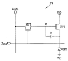
도 1은 종래의 유기발광 표시장치의 일 화소에 대한 등가 회로도를 나타낸 도면이다.1 is an equivalent circuit diagram of one pixel of a conventional OLED display.
도시된 바와 같이, 유기발광 표시장치는 스캔신호(Scan)배선 및 데이터 신호(Vdata)배선이 교차 형성되고, 이와 소정간격 이격되어 전원전압(VDD)를 공급하는 배선이 형성되어, 하나의 화소(PX)을 정의한다.As shown in the figure, the organic light emitting display device includes a scan line and a data line, which are formed by intersecting scan lines and data lines, PX).
또한, 스캔신호(Scan)에 대응하여 데이터 신호(Vdata)를 제1 노드(N1)에 인가하는 스위칭 박막트랜지스터(STFT)와, 소스전극에 구동전압(VDD)을 인가받으며, 제1 노드(N1)에 인가된 전압에 따라 드레인 전류를 유기전계 발광다이오드(Organic Light-Emitting Diode, OLED)에 인가하는 구동 박막트랜지스터(DTFT)와, 구동 박막트랜지스터(DTFT)의 게이트 전극에 인가되는 전압을 1 프레임 동안 유지시키는 캐패시터(C1)를 포함한다. A switching thin film transistor STFT applying a data signal Vdata to the first node N1 in response to the scan signal Scan and a second thin film transistor ST2 receiving a driving voltage VDD from the source electrode, A driving thin film transistor DTFT for applying a drain current to an organic light emitting diode (OLED) according to a voltage applied to the driving thin film transistor DTFT, Gt; C1 < / RTI >
그리고, 유기전계 발광다이오드(OLED)는 구동 박막트랜지스터(DTFT)의 드레인전극에 애노드전극이 접속되며, 캐소드전극이 접지(VSS)되며, 캐소드전극과 애노드전극사이에 형성되는 유기발광층을 포함한다. 전술한 유기발광층은 정공수송층, 발광층 및 전자수송층으로 구성될 수 있다.The organic light emitting diode OLED includes an anode electrode connected to the drain electrode of the driving thin film transistor DTFT, a cathode electrode Vss connected to the cathode electrode, and an organic emission layer formed between the cathode electrode and the anode electrode. The above-described organic luminescent layer may be composed of a hole transporting layer, a luminescent layer and an electron transporting layer.
전술한 유기발광 표시장치는 구동 박막트랜지스터(DTFT)에 의해 유기전계 발광다이오드에 흐르는 전류의 양을 조절하여 영상의 계조를 표시하는 것으로, 구동 박막트랜지스터(DTFT)의 특성에 의해 화질이 결정된다.The organic light emitting display device displays the gray level of an image by controlling the amount of current flowing in the organic light emitting diode by a driving thin film transistor (DTFT). The image quality is determined by the characteristics of the driving thin film transistor (DTFT).
그러나, 하나의 표시패널 내에서도 각 화소간 구동 박막트랜지스터(DTFT)들의 문턱전압(threshold voltage)에 편차가 존재하며, 이에 따라 유기전계 발광다이오드(OLED)들에 흐르는 전류가 변화하여 원하는 계조를 구현하지 못하는 문제가 발생하게 된다. 또한, 유기전계 발광다이오드(OLED)의 턱전압의 편차에 따라 흐르는 전류가 영향을 받게 된다. However, even within one display panel, there is a variation in the threshold voltage of the inter-pixel driving TFTs (DTFTs), so that the current flowing in the organic light emitting diodes OLEDs changes, A problem that can not be solved occurs. Also, the current flowing depending on the deviation of the threshold voltage of the organic light emitting diode (OLED) is affected.
도 2는 종래 유기발광 표시장치의 구동 박막트랜지스터 문턱전압 특성에 따른 전류특성을 그래프로 나타낸 도면이다.2 is a graph illustrating a current characteristic according to a threshold voltage characteristic of a driving thin film transistor of a conventional OLED display device.
도시된 바와 같이, 종래의 유기발광 표시장치에서 구동 박막트랜지스터의 게이트 전극에 데이터전압(Vd)이 인가되면, 게이트-소스간 전압(Vgs)에 따라 드레인-소스간 전류가 흐르게 되며, 이는 유기전계 발광다이오드(IOLED)에 흐르는 전류가 된다.As shown, when the data voltage Vd is applied to the gate electrode of the driving thin film transistor in the conventional OLED display device, the drain-source current flows according to the gate-source voltage Vgs, And becomes a current flowing in the light emitting diode IOLED.
이때, 구동 트랜지스터의 문턱전압(Vth)이 설계보다 낮거나, 전자이동도(μ)가 높은 특성을 갖는 갖는 경우, 구동 트랜지스터의 I-V 커브는 a로 변한다. 또한, 문턱전압(Vth)이 설계보다 높거나, 전자이동도(μ)가 낮은 특성을 갖는 갖는 경우, I-V 커브는 b로 변하게 된다. At this time, when the threshold voltage (Vth) of the driving transistor is lower than the design value or the electron mobility (μ) is high, the I-V curve of the driving transistor changes to a. Further, when the threshold voltage Vth is higher than the design value and the electron mobility is low, the I-V curve changes to b.
또한, 유기전계 발광 다이오드에 흐르는 전류에 영향을 주는 인자로서, 유기전계 발광 다이오드의 문턱전압(Vth)이 상승함에 따라, I-V 커브는 c로 변하게 된다.Further, as the threshold voltage (Vth) of the organic light emitting diode increases as a factor affecting the current flowing in the organic electroluminescent diode, the I-V curve changes to c.
전술한 I-V 커브변화에 대응하는 전류편차는 유기발광 표시장치에서 MURA, 잔상 및 수명감소 등과 같은 불량의 원인이 된다. The current deviation corresponding to the I-V curve change described above causes defects such as MURA, afterimage, and life span in the OLED display device.
본 발명은 전술한 문제점을 해결하기 위해 안출된 것으로, 본 발명의 목적은 구동 박막트랜지스터 및 유기전계 발광다이오드의 특성편차에 따라 발생하는 전류편차 문제를 개선하는 보상회로를 포함하는 유기발광 표시장치를 제공하는 데 있다. It is an object of the present invention to provide an organic light emitting display device including a driving thin film transistor and a compensation circuit for improving a current deviation problem caused by a characteristic deviation of the organic light emitting diode .
전술한 목적을 달성하기 위해, 본 발명의 바람직한 실시예에 따른 유기발광 표시장치복수의 게이트 배선 및 데이터 배선이 교차배치되고, 교차지점에 화소를 정의하는 표시패널; 상기 게이트 배선 및 데이터 배선을 구동하는 게이트 구동부 및 데이터 구동부; 상기 게이트 구동부 및 데이터 구동부를 제어하는 타이밍 콘트롤러; 및 전원전압 공급배선을 통해 상기 화소에 전원전압을 공급하며, 상기 표시패널의 내부저항에 의한 상기 전원전압의 전압강하 정도를 감지하고, 감지결과를 통해 상기 화소의 전류 편차를 보상하는 보상회로부를 포함한다. In order to achieve the above object, an organic light emitting display according to a preferred embodiment of the present invention includes: a display panel in which a plurality of gate wirings and data wirings are cross-arranged and pixels are defined at intersections; A gate driving unit and a data driving unit driving the gate wiring and the data wiring; A timing controller for controlling the gate driver and the data driver; And a compensation circuit for supplying a power supply voltage to the pixel through a power supply voltage supply line, detecting a voltage drop of the power supply voltage due to an internal resistance of the display panel, and compensating for a current deviation of the pixel through a detection result .
상기 보상 회로부는, 상기 전원전압 공급배선에 직렬연결되어 상기 화소에 전원전압의 공급을 제어하는 제1 스위칭 소자; 상기 전원전압 공급배선에 병렬연결되어 상기 화소에 전원전압의 공급을 제어하는 제2 스위칭 소자; 상기 제2 스위칭 소자와 직렬연결되어 상기 화소에 흐르는 전류를 산출하기 위한 저항값을 갖는 저항 소자; 및 상기 전원전압 공급배선과 병렬연결되어 상기 저항 소자에 의한 전압강하 값을 감지하는 전압 감지부를 포함하는 것을 특징으로 한다. Wherein the compensation circuit comprises: a first switching element connected in series to the power supply voltage supply wiring to control supply of a power supply voltage to the pixel; A second switching device connected in parallel to the power supply voltage supply line to control supply of a power supply voltage to the pixel; A resistance element connected in series with the second switching element and having a resistance value for calculating a current flowing to the pixel; And a voltage sensing unit connected in parallel to the power supply voltage supply line to sense a voltage drop value of the resistance device.
상기 보상 회로부는, 상기 제1 스위칭 소자 및 제2 스위칭 소자와 병렬로 연결되며, 상기 전원전압 공급배선과 상기 전압 감지부사이에 연결되는 노이즈 제거 캐패시터를 더 포함하는 것을 특징으로 한다. The compensation circuit unit may further include a noise removal capacitor connected in parallel to the first and second switching devices and connected to the power supply voltage supply line and the voltage sensing device.
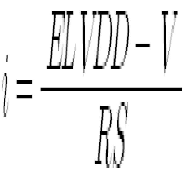
상기 전압 감지부는, 감지된 전압 강하값과, 상기 전원전압 및 상기 저항값을 통해 상기 화소의 전류값을 산출하는 것을 특징으로 한다. The voltage sensing unit may calculate a current value of the pixel through the sensed voltage drop value, the power supply voltage, and the resistance value.
상기 화소의 전류값(i)는 상기 전원전압을 ELVDD, 상기 저항값을 RS, 상기 감지된 전압 강하값을 V라 할 때, 수학식The current value (i) of the pixel may be expressed by the following equation when the power source voltage is ELVDD, the resistance value is RS, and the sensed voltage drop value is V,

를 만족하는 것을 특징으로 한다. . ≪ / RTI >
상기 타이밍 콘트롤러는, 상기 전류값에 따라 상기 데이터 전압의 보상정도를 결정하는 데이터 전압보상 수단이 더 포함되는 것을 특징으로 한다. The timing controller may further include data voltage compensation means for determining a degree of compensation of the data voltage according to the current value.
전술한 목적을 달성하기 위해, 본 발명의 바람직한 실시예에 따른 유기발광 표시장치의 구동방법은, 전원전압 공급배선을 통해 표시패널의 화소에 전원전압을 공급하며, 상기 표시패널의 내부저항에 의한 상기 전원전압의 전압강하 정도를 감지하고, 감지결과를 통해 상기 화소의 전류 편차를 보상하는 보상회로부를 포함하는 유기발광 표시장치의 구동방법에 있어서, 상기 전원전압을 감지하는 단계; 상기 보상회로부에 내장된 저항소자를 통해 전압강하된 전원전압을 감지하는 단계; 감지된 전압강하값, 상기 전원전압 및 상기 저항소자의 저항값을 통해 상기 화소의 전류값을 산출하는 단계; 및 산출된 전류값에 대응하여 상기 화소에 인가되는 데이터 전압을 보상하는 단계를 포함한다. According to an aspect of the present invention, there is provided a method of driving an organic light emitting display, including: supplying a power source voltage to a pixel of a display panel through a power supply voltage supply line; And a compensation circuit for sensing a voltage drop of the power supply voltage and compensating for a current deviation of the pixel through a detection result, the method comprising: sensing the power supply voltage; Sensing a power supply voltage that has been dropped through a resistance element built in the compensation circuit; Calculating a current value of the pixel through the sensed voltage drop value, the power supply voltage, and the resistance value of the resistance element; And compensating a data voltage applied to the pixel corresponding to the calculated current value.
상기 감지된 전압강하값, 상기 전원전압 및 상기 저항소자의 저항값을 통해 상기 화소의 전류값을 산출하는 단계는, 상기 화소에 255 계조의 데이터전압을 공급하는 단계를 포함하는 것을 특징으로 한다. The step of calculating the current value of the pixel through the sensed voltage drop value, the power supply voltage, and the resistance value of the resistance element may include supplying a data voltage of 255 gray levels to the pixel.
감지된 전압강하값, 상기 전원전압 및 상기 저항소자의 저항값을 통해 상기 화소의 전류값을 산출하는 단계는, 모든 화소를 하나씩 순차적으로 구동시켜 진행하는 것을 특징으로 한다. The step of calculating the current value of the pixel through the sensed voltage drop value, the power supply voltage, and the resistance value of the resistance element sequentially drives all the pixels one by one.
감지된 전압강하값, 상기 전원전압 및 상기 저항소자의 저항값을 통해 상기 화소의 전류값을 산출하는 단계는, 동일 수평선상의 화소를 동시에 구동시켜 하나의 수평선씩 순차적으로 진행하는 것을 특징으로 한다. The step of calculating the current value of the pixel through the sensed voltage drop value, the power supply voltage, and the resistance value of the resistive element sequentially drives the pixels on the same horizontal line one by one along the horizontal line.
감지된 전압강하값, 상기 전원전압 및 상기 저항소자의 저항값을 통해 상기 화소의 전류값을 산출하는 단계는, 인접한 복수의 화소를 동시에 구동시켜 블록단위로 진행하되, 전후 블록의 화소가 중첩되도록 진행하는 것을 특징으로 한다. The step of calculating the current value of the pixel through the sensed voltage drop value, the power supply voltage, and the resistance value of the resistive element may be performed by simultaneously driving a plurality of adjacent pixels so that the pixels of the previous and next blocks overlap each other .
본 발명의 실시예에 따르면, 서로 다른 전류패스를 통해 소정 노드의 전압을 감지하는 포함하는 보상회로부를 통해 화소에 인가되는 전원전압의 전압강화 정도를 센싱하고, 이에 따라 데이터전압을 보상하여 유기발광 표시장치의 각 화소의 전류편차에 따른 화질저하 및 수명감소 등의 문제점을 개선할 수 있는 효과가 있다. According to an embodiment of the present invention, a voltage compensation level of a power supply voltage applied to a pixel is sensed through a compensation circuit section that detects a voltage of a predetermined node through different current paths, There is an effect that the problems such as deterioration of the image quality and the life span due to the current deviation of each pixel of the display device can be improved.
도 1은 종래의 유기발광 표시장치의 일 화소에 대한 등가 회로도를 나타낸 도면이다.
도 2는 종래 유기발광 표시장치의 구동 박막트랜지스터 문턱전압 특성에 따른 전류특성을 그래프로 나타낸 도면이다.
도 3은 본 발명의 실시예에 따른 유기발광 표시장치의 전체 구조를 나타내는 도면이다.
도 4는 본 발명의 실시예에 따른 보상 회로부 및 이와 연결되는 표시패널상의 하나의 화소구조를 나타낸 도면이다.
도 5a 및 도 5b는 보상 회로부의 각각 전원전압(ELVDD)및 전압강하된 전원전압(ELVDD) 감지시의 전류패스를 나타낸 도면이고, 도 6은 보상 회로부 및 화소에 인가되는 신호파형을 나타내는 도면이다.
도 7a 내지 도 7c는 각 화소에 흐르는 전류의 편차를 구하는 형태를 나타낸 도면이다.1 is an equivalent circuit diagram of one pixel of a conventional OLED display.
2 is a graph illustrating a current characteristic according to a threshold voltage characteristic of a driving thin film transistor of a conventional OLED display device.
3 is a diagram illustrating an overall structure of an OLED display according to an exemplary embodiment of the present invention.
4 is a view illustrating one pixel structure on a compensation circuit portion and a display panel connected thereto according to an embodiment of the present invention.
FIGS. 5A and 5B are diagrams showing current paths when the power supply voltage ELVDD and the voltage-dropped power supply voltage ELVDD are sensed by the compensation circuit portion, respectively, and FIG. 6 is a diagram showing signal waveforms applied to the compensation circuit portion and the pixels .
Figs. 7A to 7C are diagrams showing a manner of obtaining a deviation of a current flowing in each pixel. Fig.
이하, 도면을 참조하여 본 발명의 바람직한 실시예에 따른 보상회로 및 이를 포함하는 유기발광 표시장치를 설명한다.Hereinafter, a compensation circuit according to a preferred embodiment of the present invention and an OLED display including the same will be described with reference to the drawings.
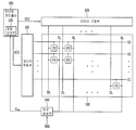
도 3은 본 발명의 실시예에 따른 유기발광 표시장치의 전체 구조를 나타내는 도면이다.3 is a diagram illustrating an overall structure of an OLED display according to an exemplary embodiment of the present invention.
도시된 바와 같이, 본 발명의 유기발광 표시장치는 다수의 화소가 정의되는 표시패널(100)와, 표시패널(100)과 연결되는 각종 구동부 및 콘트롤러(110, 120, 130)와, 보상 회로부(140)를 포함한다.As shown in the figure, the OLED display of the present invention includes a
표시패널(100)은 유기기판 또는 플라스틱 기판상에 서로 교차되도록 복수의 게이트 배선(GL) 및 데이터 배선(DL)이 형성되고, 게이트 배선(GL) 및 데이터 배선(DL)이 교차하는 지점에 각각 적(R), 녹(G) 및 청(B) 에 해당하는 화소(PX)들이 정의된다. 또한, 표시패널(100)에는 데이터 배선(DL)과 평행한 방향으로 형성되는 전원전압 공급배선(VL)이 더 형성되어 각 화소들(PX)과 연결된다. The
표시패널(100)의 각 배선(GL, DL)들은 표시패널(100)의 외곽에 형성되며 게이트 배선(GL)들에 스캔신호를 인가하는 게이트 구동부(110)와, 데이터 배선(DL)들에 데이터신호를 인가하는 데이터 구동부(120)와 연결된다. Each of the wirings GL and DL of the
또한, 표시패널(100)에 형성되는 전원전압 공급배선(VL)은 전원전압(ELVDD)이 공급되는 보상회로부(140)와 연결된다. 여기서, 도시되어 있지는 않지만, 전원공급부는 전원전압(ELVDD)뿐만 아니라, 접지전압(ELVSS)등의 표시장치의 구동을 위한 전압 등을 공급한다. 본 발명에서는 표시패널(100)에 형성된 전원전압 공급배선(VL)에 인가되는 전원전압(ELVDD)을 보상회로부(140)를 통해 공급하게 된다.The power supply voltage supply line VL formed in the
또한, 도시하지는 않았지만 상기 화소(PX)들은 적어도 하나의 유기전계 발광다이오드, 캐패시터, 스위칭 박막트랜지스터 및 구동 박막트랜지스터를 포함한다. 여기서, 유기전계 발광다이오드는 제 1 전극(정공주입 전극)과 유기 화합물층 및 제 2 전극(전자주입 전극)로 이루어질 수 있다.Also, although not shown, the pixels PX include at least one organic light emitting diode, a capacitor, a switching thin film transistor, and a driving thin film transistor. Here, the organic light emitting diode may include a first electrode (hole injection electrode), an organic compound layer, and a second electrode (electron injection electrode).
유기 화합물층은 실제 발광이 이루어지는 발광층 이외에 정공 또는 전자의 캐리어를 발광층까지 효율적으로 전달하기 위한 다양한 유기층들을 더 포함할 수 있다. 이러한 유기층들은 제 1 전극과 발광층 사이에 위치하는 정공주입층 및 정공수송층, 제 2 전극과 발광층 사이에 위치하는 전자주입층 및 전자수송층일 수 있다.The organic compound layer may further include various organic layers for efficiently transporting carriers of holes or electrons to the light-emitting layer in addition to the light-emitting layer in which light is actually emitted. These organic layers may be a hole injecting layer and a hole transporting layer positioned between the first electrode and the light emitting layer, an electron injecting layer and an electron transporting layer positioned between the second electrode and the light emitting layer.
또한, 스위칭 및 구동 박막트랜지스터들은 게이트배선(GL) 및 제어신호 공급배선(CL)과 데이터배선(DL)에 연결되며, 게이트배선(GL)에 입력되는 게이트 전압에 따라 스위칭 박막트랜지스터들이 도통되고, 동시에 데이터배선(DL)에 입력되는 데이터 전압을 구동 박막트랜지스터로 전송한다. 캐패시터는 박막트랜지스터와 전원공급배선에 사이에 연결되며, 박막트랜지스터로부터 전송되는 데이터전압으로 충전되어 1 프레임동안 유지하게 된다.The switching and driving thin film transistors are connected to the gate wiring GL and the control signal supply wiring CL and the data wiring DL so that the switching thin film transistors are made conductive in accordance with the gate voltage inputted to the gate wiring GL, At the same time, the data voltage inputted to the data line DL is transferred to the driving thin film transistor. The capacitor is connected between the thin film transistor and the power supply wiring, and is charged with the data voltage transmitted from the thin film transistor and held for one frame.
그리고, 구동 박막트랜지스터는 전원공급배선(VL)과 캐패시터에 연결되고, 게이트-소스간 전압에 대응하는 드레인 전류를 유기전계 발광다이오드로 공급한다. 이에 따라 유기전계 발광다이오드는 드레인 전류에 의해 발광하게 된다. 여기서, 구동 박막트랜지스터는 게이트전극과 소스전극 및 드레인전극을 포함하며, 유기전계 발광다이오드의 애노드 전극은 구동 박막트랜지스터의 일 전극에 연결된다. The driving thin film transistor is connected to the power supply wiring (VL) and the capacitor, and supplies a drain current corresponding to the gate-source voltage to the organic light emitting diode. Accordingly, the organic light emitting diode emits light by the drain current. Here, the driving thin film transistor includes a gate electrode, a source electrode and a drain electrode, and an anode electrode of the organic light emitting diode is connected to one electrode of the driving thin film transistor.
게이트 구동부(110)는 게이트 제어신호(GCS)에 대응하여 각 화소들(PX)에 게이트 전압을 하나의 수평선 단위씩 순차적으로 인가한다. 이러한 게이트 구동부(110)는 1 수평기간마다 하이레벨의 게이트 전압을 순차적으로 출력하는 다수의 스테이지를 갖는 쉬프트 레지스터로 구현될 수 있다.The
데이터 구동부(120)는 타이밍 콘트롤러(130)로부터 인가되는 디지털 파형의 영상신호를 입력받아 화소(PX)가 처리할 수 있는 계조값을 갖는 아날로그 전압형태의 데이터 전압으로 변환하고, 또한 입력되는 데이터 제어신호(DCS)에 대응하여 데이터 배선(DL)을 통해 각 화소(PX)에 데이터 전압을 공급한다. The
여기서, 데이터 구동부(120)는 기준전압 공급부(미도시)로부터 공급되는 다수의 기준전압을 이용하여 영상신호를 데이터 전압으로 변환하게 된다.Here, the
타이밍 콘트롤러(140)는 외부로부터 인가되는 영상신호와, 클럭신호, 수직 및 수평동기신호 등의 타이밍 신호를 인가받아, 게이트 제어신호(GCS) 및 데이터 제어신호(DCS)를 생성한다. The
여기서, 수평동기신호는 화면의 한 라인을 표시하는 데 걸리는 시간을 나타내고, 수직동기신호는 한 프레임의 화면을 표시하는 데 걸리는 시간을 나타낸다. 또한, 클록신호는 게이트 및 각 구동부의 제어신호의 생성 기준이 되는 신호이다. Here, the horizontal synchronizing signal represents the time taken to display one line of the screen, and the vertical synchronizing signal represents the time taken to display the screen of one frame. The clock signal is a signal that is a reference for generating the control signals of the gate and each driver.
한편, 도시하지는 않았지만, 타이밍 콘르롤러(130)는 외부의 시스템과 소정의 인터페이스를 통해 연결되어 그로부터 출력되는 영상관련 신호와 타이밍신호를 잡음 없이 고속으로 수신하게 된다. 이러한 인터페이스로는 LVDS(Low Voltage Differential Signal)방식 또는 TTL(Transistor-Transistor Logic) 인터페이스 방식 등이 이용될 수 있다.Meanwhile, although not shown, the
특히, 본 발명의 실시예에 따른 타이밍 콘트롤러(130)는 각 화소의 전류편차에 따른 데이터 전압의 보상값이 정의된 전압 보상부(135)를 내장하고 있으며, 이를 통해 데이터 구동부(120)에 제공하는 영상신호에 전압 보상값을 적용하여, 이후 데이터 구동부(120)에 의해 변환된 데이터 전압에 전압 보상값이 반영되도록 한다.In particular, the
또는, 데이터 구동부(120)에 제공되는 기준전압에 전압 보상값이 반영되는 형태로 구성되거나, 데이터 구동부(120)의해 변환된 데이터 전압의 전압레벨을 전압 보상값에 대응하여 조절하는 구조로 구현될 수 있다. Alternatively, a voltage compensation value may be reflected in a reference voltage provided to the
전압 보상부(135)는 보상 회로부(140)로부터 인가되는 전압감지 결과신호에 대응하여 상기 전압 보상값(Vres)을 산출하게 된다. The
보상 회로부(140)는 전원공급부(미도시)로부터 전원전압(ELVDD)을 인가받으며, 이를 표시패널(100)의 각 전원공급배선(VL)으로 공급하는데, 적어도 2개의 전류패스를 갖도록 구성되며, 초기 전원전압(ELVDD) 공급시 또는 정상구동시에 이용되는 하나의 전류패스와, 전원전압(ELVDD)의 전압강하시 전압을 감지하기 위해 이용되는 다른 전류패스가 형성되어 있다. 또한, 보상 회로부(140)는 내부 일 노드에 인가되는 전압의 레벨을 감지하는 전압 감지부를 포함한다.The
이러한 구조에 따라, 보상 회로부(140)는 제1 및 제2 전류패스에 대한 전압레벨을 감지하고, 전류패스내에 포함된 수동소자를 통해 화소에 흐르는 전류를 산출한 후, 그 결과를 전술한 타이밍 콘트롤러의 전압 보상부에 제공함으로서 각 화소간 전류편차를 보상한다.According to this structure, the
즉, 본 발명의 실시예에 따른 유기발광 표시장치는 전체 화소에 인가되는 전원전압(VDD)의 전압강하 정도와, 보상 회로부 내부에 저항소자를 통해 화소로 흐르는 전류값을 이용하여 데이터신호를 보상하는 보상회로부를 포함하는 것을 특징으로 한다. 이하, 도면을 참조하여, 본 발명의 실시예에 따른 유기발광 표시장치에 포함된 보상 회로부의 구조를 설명한다.That is, the organic light emitting display according to the embodiment of the present invention compensates the data signal by using the voltage drop degree of the power supply voltage VDD applied to all pixels and the current value flowing into the pixel through the resistance element in the compensation circuit portion And a compensating circuit portion for compensating the voltage of the output signal. Hereinafter, a structure of a compensation circuit included in an organic light emitting display according to an embodiment of the present invention will be described with reference to the drawings.
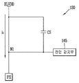
도 4는 본 발명의 실시예에 따른 보상 회로부 및 이와 연결되는 표시패널상의 하나의 화소구조를 나타낸 도면이다.4 is a view illustrating one pixel structure on a compensation circuit portion and a display panel connected thereto according to an embodiment of the present invention.
도면을 참조하면, 본 발명의 일 화소는 스캔신호(Scan)배선 및 데이터 신호(Vdata)배선이 교차 형성되고, 이와 소정간격 이격되어 전원전압(VDD)를 공급하는 배선이 형성되어, 하나의 화소(PX)을 정의한다.Referring to the drawings, one pixel of the present invention includes a scan line (scan line) and a data signal (Vdata) line intersecting with each other and a wiring line spaced apart from the scan line by a predetermined distance to supply a power source voltage VDD, (PX).
또한, 스캔신호(Scan)에 대응하여 데이터 신호(Vdata)를 제1 노드(N1)에 인가하는 스위칭 박막트랜지스터(STFT)와, 소스전극에 구동전압(VDD)을 인가받으며, 제1 노드(N1)에 인가된 전압에 따라 드레인 전류를 유기전계 발광다이오드(Organic Light-Emitting Diode, OLED)에 인가하는 구동 박막트랜지스터(DTFT)와, 구동 박막트랜지스터(DTFT)의 게이트 전극에 인가되는 전압을 1 프레임 동안 유지시키는 캐패시터(C1)를 포함한다.A switching thin film transistor STFT applying a data signal Vdata to the first node N1 in response to the scan signal Scan and a second thin film transistor ST2 receiving a driving voltage VDD from the source electrode, A driving thin film transistor DTFT for applying a drain current to an organic light emitting diode (OLED) according to a voltage applied to the driving thin film transistor DTFT, Gt; C1 < / RTI >
그리고, 전술한 일 화소(PX)의 전원전압(ELVDD) 공급배선은 표시패널의 외측에서 보상회로부(140)와 연결된다.The power supply voltage ELVDD supply wiring of one pixel PX is connected to the
보상 회로부(140)는 전원전압(ELVDD) 공급배선에 직렬연결되어 화소(PX)에 전원전압의 공급을 제어하는 제1 스위칭 소자(SW1)와, 전원전압(ELVDD) 공급배선에 병렬연결되어 화소(PX)에 전원전압(ELVDD)의 공급을 제어하는 제2 스위칭 소자(SW2)와, 제2 스위칭 소자(SW2)와 직렬연결되어 화소(PX)에 흐르는 전류를 산출하기 위한 저항값을 갖는 저항 소자(RS)와, 전원전압(ELVDD) 공급배선과 병렬연결되어 저항 소자(RS)에 의한 전압강하 값을 감지하는 전압 감지부(145)를 포함한다.The
여기서, 제1 스위칭 소자(SW1)는 제1 제어신호(VS1)에 의해 도통되며, 전원전압(ELVDD)에 의한 화소전류의 제1 전류패스를 형성한다. 또한, 제2 스위칭 소자(SW2)는 제2 제어신호(VS2)에 의해 도통되며, 저항 소자(RS)와 함께 화소전류의 제2 전류패스를 형성하게 된다.Here, the first switching device SW1 is conducted by the first control signal VS1 and forms the first current path of the pixel current by the power source voltage ELVDD. Further, the second switching element SW2 is conducted by the second control signal VS2, and forms a second current path of the pixel current together with the resistance element RS.
그리고, 제1 스위칭 소자(SW1) 및 제2 스위칭 소자(SW2)와 병렬로 연결되며, 전원전압 공급배선(ELVDD)과 전압 감지부 사이에 연결되는 노이즈 제거 캐패시터(CS)를 더 포함 할 수 있다. 이러한 노이즈 제거 캐패시터(CS)는 외부로부터 유입되는 정전기나 기타 전압성분에 의해 전류가 반대방향으로 흐르는 현상을 방지하기 위해 구비되는 것으로 생략될 수 있다.The first switch SW1 and the second switch SW2 may further include a noise removing capacitor CS connected in parallel and connected between the power supply voltage supply line ELVDD and the voltage sensing unit . Such a noise removing capacitor CS may be omitted in order to prevent the current from flowing in the opposite direction due to static electricity or other voltage components flowing from the outside.
이하, 보상 회로부(130)에 인가되는 신호의 파형을 참조하여 본 발명의 실시예에 따른 유기발광 표시장치의 구동방법을 설명한다.Hereinafter, a method of driving the OLED display according to an exemplary embodiment of the present invention will be described with reference to waveforms of signals applied to the
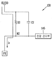
도 5a 및 도 5b는 보상 회로부의 각각 전원전압(ELVDD)및 전압강하된 전원전압(ELVDD) 감지시의 전류패스를 나타낸 도면이고, 도 6은 보상 회로부 및 화소에 인가되는 신호파형을 나타내는 도면이다.FIGS. 5A and 5B are diagrams showing current paths when the power supply voltage ELVDD and the voltage-dropped power supply voltage ELVDD are sensed by the compensation circuit portion, respectively, and FIG. 6 is a diagram showing signal waveforms applied to the compensation circuit portion and the pixels .
먼저 도 5a 및 도 6을 참조하면, 보상 회로부(130)에는 화소의 초기화 단계 또는 보상된 데이터전압의 인가단계에서 제1 제어신호(VS1)가 하이레벨로 인가되고, 제2 제어신호(VS2)가 로우레벨로 인가됨에 따라 제1 스위칭 소자(SW1)가 턴-온되어 제1 노드(N1)를 거쳐 전원전압(ELVDD)배선과 화소(PX)사이에 제1 전류패스(i1)가 형성된다.5A and 6, the first control signal VS1 is applied at a high level and the second control signal VS2 is applied to the
동시에 최대계조를 나타내는 로우레벨의 데이터전압(VDATA)이 인가되면, 제1 전류패스(i1)를 통해 최대량의 전류가 화소로 흐르게 된다. 이때, 제1 노드(N1)에는 전원전압(VDD)이 인가되며, 전압 감지부(145)는 초기 VDD 전압의 레벨을 감지하게 된다.At the same time, when a low level data voltage VDATA indicating the maximum gradation is applied, a maximum amount of current flows to the pixel through the first current path i1. At this time, the power supply voltage VDD is applied to the first node N1, and the
이후, 도 5b 및 도 6을 참조하면, 보상 회로부(130)에는 센싱단계에서 제1 제어신호(VS1)가 로우레벨로 인가되고, 제2 제어신호(VS2)가 하이레벨로 인가됨에 따라, 제1 스위칭 소자(SW1)는 턴-오프되고, 제2 스위칭 소자(SW2)는 턴-온되어 제2 노드(N2)를 거쳐 전원전압(ELVDD)배선과 화소(PX)사이에 제2 전류패스(i2)가 형성된다.5B and 6, the first control signal VS1 is applied to the
본 단계에서는 영상을 표시하는 것이 아닌, 화소(PX)의 전류특성을 감지하기 위한 것이므로 데이터 전압(VDATA)은 최소계조인 하이레벨의 데이터전압(VDATA)이 인가될 수 있다.In this step, since the current characteristic of the pixel PX is sensed instead of displaying the image, the data voltage VDATA can be applied to the data voltage VDATA of the high level which is the minimum gradation.
이에 따라, 제2 전류패스(i2)를 통해 전류가 화소로 흐르게 된다. 이때, 제2 노드(N2)에는 저항소자(RS)에 의해 전압강하된 전압이 인가되며, 전압 감지부(145)는 전압 강하된 전압 레벨을 감지하게 된다.As a result, current flows to the pixel through the second current path i2. At this time, a voltage lowered by the resistance element RS is applied to the second node N2, and the
즉, 제2 노드(N2)에 인가되는 전압은 이하의 수학식 1에 따라,
That is, the voltage applied to the second node N2 is expressed by the following equation (1)
![]()
![]()
가 되며, 이에 따라 제2 전류패스(i2)를 통해 흐르는 전류는,
So that the current flowing through the second current path i2,
즉, 제2 전류패스(i2)는 초기 전원전압(ELVDD), 제2 노드(N2)에 인가된 전압 및 저항소자(RS)에 의해 결정된다. 따라서, 상기 각 화소를 통해 흐르는 전류량을 산출할 수 있으며, 이를 통해 각 화소의 전류편차를 알아낼 수 있다. That is, the second current path i2 is determined by the initial power supply voltage ELVDD, the voltage applied to the second node N2, and the resistance element RS. Accordingly, the amount of current flowing through each pixel can be calculated, and the current deviation of each pixel can be obtained through the calculation.
전압 감지부는 전술한 초기화 단계 및 센싱단계를 통해 각 화소의 전류편차를 구하고, 보상단계에서 그 결과신호(Vres)를 타이밍 콘트롤러의 전압 보상부(135)에 인가하여 영상신호를 보상하거나, 또는 데이터전압을 보상하여 각 화소의 전류편차를 개선하게 된다. The voltage sensing unit obtains the current deviation of each pixel through the initialization step and the sensing step described above and supplies the resultant signal Vres to the
전술한 센싱단계는 각 화소별로 순차적으로 진행되거나, 수평선단위로 다수의 화소에 대하여 동시에 진행할 수 있으며, 또는 소정의 화소블록별로 중첩되도록 진행할 수도 있다. The sensing step may be sequentially performed for each pixel, for a plurality of pixels at a time on a horizontal line basis, or may be performed for each predetermined pixel block.
도 7a 내지 도 7b는 각 화소에 흐르는 전류의 편차를 구하는 형태를 나타낸 도면이다. Figs. 7A and 7B are diagrams showing a manner of obtaining a deviation of a current flowing in each pixel. Fig.
도 7a를 참조하면, 표시패널(100)상에 다수의 화소에 대하여 모든 화소를 하나씩 순차적으로 구동시켜 진행하는 것으로, 제1 화소(PX1)에 흐르는 전류량을 구하고, 이후 인접한 제2 화소(PX2)에 대한 화소전류를 구하게 된다. 이러한 방법은 모든 화소에 대하여 순차적으로 화소전류를 산출함에 따라 정확도가 높다는 장점이 있으나, 감지시간이 지연된다는 단점이 있다. Referring to FIG. 7A, the amount of current flowing in the first pixel PX1 is obtained by sequentially driving all the pixels one by one on the
다음으로, 도 7b는 동일 수평선상의 화소를 동시에 구동시켜 전류편차 감지를 하나의 수평선씩 순차적으로 진행하는 방법을 나타내고 있다. 먼저, 제1 화소라인(PXL1)에 흐르는 전류량을 구하고, 이후 게이트신호에 따라 제2 화소라인(PXL2)에 대한 화소전류를 구하게 된다.Next, FIG. 7B shows a method of simultaneously driving the pixels on the same horizontal line and detecting the current deviation sequentially by one horizontal line. First, the amount of current flowing through the first pixel line PXL1 is obtained, and then the pixel current for the second pixel line PXL2 is obtained according to the gate signal.
이러한 방법은 정확도는 떨어지나, 신속하게 화소전류의 편차를 구할 수 있다는 장점이 있다. 표시패널(100)의 전면에 걸쳐 공정,물리, 환경적인 특성이 유사한 경우 적용될 수 있다. This method has the advantage that the deviation of the pixel current can be quickly obtained although the accuracy is low. Physical, and environmental characteristics across the entire surface of the
또한, 도 7c를 참조하면, 인접한 복수의 화소를 동시에 구동시켜 블록단위로 전류편차 감지를 진행하되, 전후 블록의 화소가 중첩되도록 함으로서, 정확도를 높이고 감지시간을 단축할 수 있는 장점이 있다.Referring to FIG. 7C, the adjacent pixels are simultaneously driven to detect the current deviation on a block-by-block basis, and pixels of the preceding and following blocks are superimposed, thereby improving accuracy and sensing time.
전술한 설명에 많은 사항이 구체적으로 기재되어 있으나 이것은 발명의 범위를 한정하는 것이라기보다 바람직한 실시예의 예시로서 해석되어야 한다. 따라서, 발명은 설명된 실시예에 의하여 정할 것이 아니고 특허청구범위와 특허청구범위에 균등한 것에 의하여 정하여져야 한다.While a number of embodiments have been described in detail above, it should be construed as being illustrative of preferred embodiments rather than limiting the scope of the invention. Accordingly, the invention is not to be determined by the embodiments described, but should be determined by equivalents to the claims and the appended claims.
100 : 표시패널 110 : 게이트 구동부
120 : 데이터 구동부 130 : 타이밍 콘트롤러
135 : 전압 보상부 140 : 보상 회로부100: display panel 110: gate driver
120: Data driver 130: Timing controller
135: Voltage compensator 140: Compensation circuit
Claims (11)
상기 게이트 배선 및 데이터 배선을 구동하는 게이트 구동부 및 데이터 구동부;
상기 게이트 구동부 및 데이터 구동부를 제어하는 타이밍 콘트롤러; 및
전원전압 공급배선을 통해 상기 화소에 전원전압을 공급하며, 상기 표시패널의 내부저항에 의한 상기 전원전압의 전압강하 정도를 감지하고, 감지결과를 통해 상기 화소의 전류 편차를 보상하는 보상회로부
를 포함하는 유기발광 표시장치.A display panel in which a plurality of gate wirings and data wirings are cross-arranged and pixels are defined at intersections;
A gate driving unit and a data driving unit driving the gate wiring and the data wiring;
A timing controller for controlling the gate driver and the data driver; And
A compensation circuit for supplying a power supply voltage to the pixel through a power supply voltage supply line, detecting a voltage drop of the power supply voltage due to an internal resistance of the display panel, and compensating a current deviation of the pixel through a detection result,
And an organic light emitting diode (OLED).
상기 보상 회로부는,
상기 전원전압 공급배선에 직렬연결되어 상기 화소에 전원전압의 공급을 제어하는 제1 스위칭 소자;
상기 전원전압 공급배선에 병렬연결되어 상기 화소에 전원전압의 공급을 제어하는 제2 스위칭 소자;
상기 제2 스위칭 소자와 직렬연결되어 상기 화소에 흐르는 전류를 산출하기 위한 저항값을 갖는 저항 소자; 및
상기 전원전압 공급배선과 병렬연결되어 상기 저항 소자에 의한 전압강하 값을 감지하는 전압 감지부
를 포함하는 것을 특징으로 하는 유기발광 표시장치.The method according to claim 1,
Wherein the compensation circuit section comprises:
A first switching element connected in series to the power supply voltage supply wiring to control supply of a power supply voltage to the pixel;
A second switching device connected in parallel to the power supply voltage supply line to control supply of a power supply voltage to the pixel;
A resistance element connected in series with the second switching element and having a resistance value for calculating a current flowing to the pixel; And
A voltage sensing unit connected in parallel to the power supply voltage supply line to sense a voltage drop value of the resistance device,
And an organic light emitting diode (OLED).
상기 보상 회로부는,
상기 제1 스위칭 소자 및 제2 스위칭 소자와 병렬로 연결되며, 상기 전원전압 공급배선과 상기 전압 감지부사이에 연결되는 노이즈 제거 캐패시터
를 더 포함하는 것을 특징으로 하는 유기발광 표시장치.3. The method of claim 2,
Wherein the compensation circuit section comprises:
And a noise canceling capacitor connected in parallel to the first switching device and the second switching device and connected to the power supply voltage supply line and the voltage sensing device,
Wherein the organic light emitting display device further comprises an organic light emitting diode.
상기 전압 감지부는,
감지된 전압 강하값과, 상기 전원전압 및 상기 저항값을 통해 상기 화소의 전류값을 산출하는 것을 특징으로 하는 유기발광 표시장치.3. The method of claim 2,
The voltage sensing unit includes:
And calculates the current value of the pixel through the sensed voltage drop value, the power supply voltage, and the resistance value.
상기 화소의 전류값(i)는 상기 전원전압을 ELVDD, 상기 저항값을 RS, 상기 감지된 전압 강하값을 V라 할 때,
를 만족하는 것을 특징으로 하는 유기발광 표시장치.5. The method of claim 4,
The current value (i) of the pixel is set to a value obtained by dividing the power supply voltage by ELVDD, the resistance value by RS, and the sensed voltage drop value by V,
Of the organic light emitting display device.
상기 타이밍 콘트롤러는,
상기 전류값에 따라 상기 데이터 전압의 보상정도를 결정하는 데이터 전압보상 수단이 더 포함되는 것을 특징으로 하는 유기발광 표시장치.5. The method of claim 4,
The timing controller includes:
And data voltage compensation means for determining a degree of compensation of the data voltage according to the current value.
상기 전원전압을 감지하는 단계;
상기 보상회로부에 내장된 저항소자를 통해 전압강하된 전원전압을 감지하는 단계;
감지된 전압강하값, 상기 전원전압 및 상기 저항소자의 저항값을 통해 상기 화소의 전류값을 산출하는 단계; 및
산출된 전류값에 대응하여 상기 화소에 인가되는 데이터 전압을 보상하는 단계
를 포함하는 유기발광 표시장치의 구동방법.A compensation circuit for supplying a power supply voltage to pixels of a display panel through a power supply voltage supply line, detecting a voltage drop of the power supply voltage due to an internal resistance of the display panel, and compensating a current deviation of the pixel through a detection result, The method of driving an organic light emitting display device according to claim 1,
Sensing the power supply voltage;
Sensing a power supply voltage that has been dropped through a resistance element built in the compensation circuit;
Calculating a current value of the pixel through the sensed voltage drop value, the power supply voltage, and the resistance value of the resistance element; And
Compensating a data voltage applied to the pixel corresponding to the calculated current value
And a driving method of the organic light emitting display device.
상기 감지된 전압강하값, 상기 전원전압 및 상기 저항소자의 저항값을 통해 상기 화소의 전류값을 산출하는 단계는,
상기 화소에 255 계조의 데이터전압을 공급하는 단계를 포함하는 것을 특징으로 하는 유기발광 표시장치의 구동방법.8. The method of claim 7,
The step of calculating the current value of the pixel through the sensed voltage drop value, the power supply voltage, and the resistance value of the resistance element,
And supplying a data voltage of 255 gray levels to the pixel.
감지된 전압강하값, 상기 전원전압 및 상기 저항소자의 저항값을 통해 상기 화소의 전류값을 산출하는 단계는, 모든 화소를 하나씩 순차적으로 구동시켜 진행하는 것을 특징으로 하는 유기발광 표시장치의 구동방법.8. The method of claim 7,
Wherein the step of calculating the current value of the pixel through the sensed voltage drop value, the power supply voltage, and the resistance value of the resistive element sequentially drives all the pixels one by one. .
감지된 전압강하값, 상기 전원전압 및 상기 저항소자의 저항값을 통해 상기 화소의 전류값을 산출하는 단계는, 동일 수평선상의 화소를 동시에 구동시켜 하나의 수평선씩 순차적으로 진행하는 것을 특징으로 하는 유기발광 표시장치의 구동방법.8. The method of claim 7,
Wherein the step of calculating the current value of the pixel through the sensed voltage drop value, the power supply voltage, and the resistance value of the resistive element sequentially drives the pixels on the same horizontal line one at a time by one horizontal line. A method of driving a light emitting display device.
감지된 전압강하값, 상기 전원전압 및 상기 저항소자의 저항값을 통해 상기 화소의 전류값을 산출하는 단계는, 인접한 복수의 화소를 동시에 구동시켜 블록단위로 진행하되, 전후 블록의 화소가 중첩되도록 진행하는 것을 특징으로 하는 유기발광 표시장치의 구동방법.8. The method of claim 7,
The step of calculating the current value of the pixel through the sensed voltage drop value, the power supply voltage, and the resistance value of the resistive element may be performed by simultaneously driving a plurality of adjacent pixels so that the pixels of the previous and next blocks overlap each other Wherein the organic light emitting display device comprises a plurality of pixels.
Priority Applications (1)
| Application Number | Priority Date | Filing Date | Title |
|---|---|---|---|
| KR1020120146292A KR102028504B1 (en) | 2012-12-14 | 2012-12-14 | Organic light-emtting diode display device incuding compensation circuit |
Applications Claiming Priority (1)
| Application Number | Priority Date | Filing Date | Title |
|---|---|---|---|
| KR1020120146292A KR102028504B1 (en) | 2012-12-14 | 2012-12-14 | Organic light-emtting diode display device incuding compensation circuit |
Publications (2)
| Publication Number | Publication Date |
|---|---|
| KR20140077458A true KR20140077458A (en) | 2014-06-24 |
| KR102028504B1 KR102028504B1 (en) | 2019-10-04 |
Family
ID=51129393
Family Applications (1)
| Application Number | Title | Priority Date | Filing Date |
|---|---|---|---|
| KR1020120146292A Active KR102028504B1 (en) | 2012-12-14 | 2012-12-14 | Organic light-emtting diode display device incuding compensation circuit |
Country Status (1)
| Country | Link |
|---|---|
| KR (1) | KR102028504B1 (en) |
Cited By (15)
| Publication number | Priority date | Publication date | Assignee | Title |
|---|---|---|---|---|
| CN104821152A (en) * | 2015-05-28 | 2015-08-05 | 深圳市华星光电技术有限公司 | Method for compensating AMOLED voltage drop and system thereof |
| KR20160015428A (en) * | 2014-07-30 | 2016-02-15 | 삼성디스플레이 주식회사 | Organic light emitting display device and method of driving an organic light emitting display device |
| KR20160080948A (en) * | 2014-12-30 | 2016-07-08 | 엘지디스플레이 주식회사 | Organic Light Emitting Display, Image Quality Compensation Device And Method Thereof |
| KR20160094129A (en) * | 2015-01-30 | 2016-08-09 | 엘지디스플레이 주식회사 | Method and apparatus for sensing current of orgainc emitting diode display device |
| KR20160124338A (en) * | 2015-04-17 | 2016-10-27 | 삼성디스플레이 주식회사 | Data compensation device and display device including the same |
| KR20170118279A (en) * | 2016-04-14 | 2017-10-25 | 엘지디스플레이 주식회사 | Display device |
| CN109872695A (en) * | 2019-04-11 | 2019-06-11 | 深圳市华星光电半导体显示技术有限公司 | The detecting voltage correcting method of AMOLED pixel-driving circuit |
| CN110419074A (en) * | 2017-03-09 | 2019-11-05 | 硅工厂股份有限公司 | Pixel sensing device and panel driving device |
| CN111048019A (en) * | 2018-10-12 | 2020-04-21 | 三星显示有限公司 | Organic Light Emitting Display Device |
| KR20200065765A (en) * | 2018-11-30 | 2020-06-09 | 엘지디스플레이 주식회사 | Organic light emitting display apparatus |
| US10937366B2 (en) | 2018-11-21 | 2021-03-02 | Samsung Display Co., Ltd. | Pixel circuit of display apparatus |
| KR20210039880A (en) * | 2019-10-02 | 2021-04-12 | 엘지디스플레이 주식회사 | Display device and operating method of the same |
| US11087679B2 (en) | 2018-09-21 | 2021-08-10 | Samsung Display Co., Ltd. | Pixel and display device including the same |
| KR20210116735A (en) * | 2020-03-12 | 2021-09-28 | 삼성디스플레이 주식회사 | Display device and driving method thereof |
| CN114784024A (en) * | 2022-05-19 | 2022-07-22 | 广州华星光电半导体显示技术有限公司 | Display panel and preparation method thereof |
Families Citing this family (2)
| Publication number | Priority date | Publication date | Assignee | Title |
|---|---|---|---|---|
| TW202303553A (en) | 2021-06-28 | 2023-01-16 | 韓商Lx半導體科技有限公司 | Voltage drop compensation system of display panel, and display driving device for compensating for voltage drop of display panel |
| KR20230096541A (en) | 2021-12-23 | 2023-06-30 | 엘지디스플레이 주식회사 | Light emitting display apparatus and multi screen display apparatus using the same |
Citations (3)
| Publication number | Priority date | Publication date | Assignee | Title |
|---|---|---|---|---|
| KR100635582B1 (en) * | 2005-08-05 | 2006-10-17 | 삼성에스디아이 주식회사 | Organic light emitting display device |
| KR20090011701A (en) * | 2007-07-27 | 2009-02-02 | 삼성모바일디스플레이주식회사 | Organic light emitting display |
| KR20100046500A (en) * | 2008-10-27 | 2010-05-07 | 삼성전자주식회사 | Organic light emitting device, and apparatus and method of generating modification information therefor |
-
2012
- 2012-12-14 KR KR1020120146292A patent/KR102028504B1/en active Active
Patent Citations (3)
| Publication number | Priority date | Publication date | Assignee | Title |
|---|---|---|---|---|
| KR100635582B1 (en) * | 2005-08-05 | 2006-10-17 | 삼성에스디아이 주식회사 | Organic light emitting display device |
| KR20090011701A (en) * | 2007-07-27 | 2009-02-02 | 삼성모바일디스플레이주식회사 | Organic light emitting display |
| KR20100046500A (en) * | 2008-10-27 | 2010-05-07 | 삼성전자주식회사 | Organic light emitting device, and apparatus and method of generating modification information therefor |
Cited By (18)
| Publication number | Priority date | Publication date | Assignee | Title |
|---|---|---|---|---|
| KR20160015428A (en) * | 2014-07-30 | 2016-02-15 | 삼성디스플레이 주식회사 | Organic light emitting display device and method of driving an organic light emitting display device |
| KR20160080948A (en) * | 2014-12-30 | 2016-07-08 | 엘지디스플레이 주식회사 | Organic Light Emitting Display, Image Quality Compensation Device And Method Thereof |
| KR20160094129A (en) * | 2015-01-30 | 2016-08-09 | 엘지디스플레이 주식회사 | Method and apparatus for sensing current of orgainc emitting diode display device |
| KR20160124338A (en) * | 2015-04-17 | 2016-10-27 | 삼성디스플레이 주식회사 | Data compensation device and display device including the same |
| CN104821152A (en) * | 2015-05-28 | 2015-08-05 | 深圳市华星光电技术有限公司 | Method for compensating AMOLED voltage drop and system thereof |
| KR20170118279A (en) * | 2016-04-14 | 2017-10-25 | 엘지디스플레이 주식회사 | Display device |
| CN110419074B (en) * | 2017-03-09 | 2022-12-06 | 硅工厂股份有限公司 | Pixel sensing device |
| CN110419074A (en) * | 2017-03-09 | 2019-11-05 | 硅工厂股份有限公司 | Pixel sensing device and panel driving device |
| US11087679B2 (en) | 2018-09-21 | 2021-08-10 | Samsung Display Co., Ltd. | Pixel and display device including the same |
| CN111048019A (en) * | 2018-10-12 | 2020-04-21 | 三星显示有限公司 | Organic Light Emitting Display Device |
| US11227546B2 (en) | 2018-10-12 | 2022-01-18 | Samsung Display Co., Ltd. | Organic light emitting display device and method of driving the same |
| US10937366B2 (en) | 2018-11-21 | 2021-03-02 | Samsung Display Co., Ltd. | Pixel circuit of display apparatus |
| KR20200065765A (en) * | 2018-11-30 | 2020-06-09 | 엘지디스플레이 주식회사 | Organic light emitting display apparatus |
| CN109872695B (en) * | 2019-04-11 | 2021-12-28 | 深圳市华星光电半导体显示技术有限公司 | Detection voltage correction method of AMOLED pixel driving circuit |
| CN109872695A (en) * | 2019-04-11 | 2019-06-11 | 深圳市华星光电半导体显示技术有限公司 | The detecting voltage correcting method of AMOLED pixel-driving circuit |
| KR20210039880A (en) * | 2019-10-02 | 2021-04-12 | 엘지디스플레이 주식회사 | Display device and operating method of the same |
| KR20210116735A (en) * | 2020-03-12 | 2021-09-28 | 삼성디스플레이 주식회사 | Display device and driving method thereof |
| CN114784024A (en) * | 2022-05-19 | 2022-07-22 | 广州华星光电半导体显示技术有限公司 | Display panel and preparation method thereof |
Also Published As
| Publication number | Publication date |
|---|---|
| KR102028504B1 (en) | 2019-10-04 |
Similar Documents
| Publication | Publication Date | Title |
|---|---|---|
| KR102028504B1 (en) | Organic light-emtting diode display device incuding compensation circuit | |
| JP6654363B2 (en) | Organic light emitting display | |
| KR101969436B1 (en) | Driving method for organic light emitting display | |
| CN104700773B (en) | Organic light-emitting display device and its driving method | |
| KR101374477B1 (en) | Organic light emitting diode display device | |
| US9634070B2 (en) | Organic light emitting display device | |
| KR102091485B1 (en) | Organic light emitting display device and method for driving thereof | |
| KR102416682B1 (en) | Organic light emitting diode display | |
| KR102182129B1 (en) | Organic light emitting diode display and drving method thereof | |
| CN101980330B (en) | Pixel drive circuit for organic light emitting diodes | |
| KR102104254B1 (en) | Organic light emitting display device and method of driving the same | |
| KR102059806B1 (en) | Pixel, display device comprising the same and driving method thereof | |
| CN104575374A (en) | Organic light emitting diode display device and driving method thereof | |
| KR20160007786A (en) | Display device | |
| KR20140067583A (en) | Organic light emitting diode display device and method for driving the same | |
| KR101907962B1 (en) | Organic light emitting diode display device | |
| CN104575377A (en) | Pixel circuit and driving method thereof as well as active matrix organic light emitting display | |
| KR101596961B1 (en) | Organic light emitting diode display device and driving method thereof | |
| KR101901757B1 (en) | Organic light emitting diode display device and method of driving the same | |
| KR102026196B1 (en) | Organic light emitting diode display device and driving method thereof | |
| KR101970573B1 (en) | Organic light-emitting diode display device and driving method thereof | |
| KR102407490B1 (en) | Light Emitting Display Device and Driving Method thereof | |
| KR102319202B1 (en) | Organic light emitting display device | |
| KR20080082820A (en) | Organic light emitting diode display and its driving method | |
| KR101962810B1 (en) | Organic light emitting display device |
Legal Events
| Date | Code | Title | Description |
|---|---|---|---|
| PA0109 | Patent application |
St.27 status event code: A-0-1-A10-A12-nap-PA0109 |
|
| PG1501 | Laying open of application |
St.27 status event code: A-1-1-Q10-Q12-nap-PG1501 |
|
| P22-X000 | Classification modified |
St.27 status event code: A-2-2-P10-P22-nap-X000 |
|
| R17-X000 | Change to representative recorded |
St.27 status event code: A-3-3-R10-R17-oth-X000 |
|
| A201 | Request for examination | ||
| PA0201 | Request for examination |
St.27 status event code: A-1-2-D10-D11-exm-PA0201 |
|
| D13-X000 | Search requested |
St.27 status event code: A-1-2-D10-D13-srh-X000 |
|
| D14-X000 | Search report completed |
St.27 status event code: A-1-2-D10-D14-srh-X000 |
|
| E902 | Notification of reason for refusal | ||
| PE0902 | Notice of grounds for rejection |
St.27 status event code: A-1-2-D10-D21-exm-PE0902 |
|
| E13-X000 | Pre-grant limitation requested |
St.27 status event code: A-2-3-E10-E13-lim-X000 |
|
| P11-X000 | Amendment of application requested |
St.27 status event code: A-2-2-P10-P11-nap-X000 |
|
| P13-X000 | Application amended |
St.27 status event code: A-2-2-P10-P13-nap-X000 |
|
| E902 | Notification of reason for refusal | ||
| PE0902 | Notice of grounds for rejection |
St.27 status event code: A-1-2-D10-D21-exm-PE0902 |
|
| P11-X000 | Amendment of application requested |
St.27 status event code: A-2-2-P10-P11-nap-X000 |
|
| P13-X000 | Application amended |
St.27 status event code: A-2-2-P10-P13-nap-X000 |
|
| E701 | Decision to grant or registration of patent right | ||
| PE0701 | Decision of registration |
St.27 status event code: A-1-2-D10-D22-exm-PE0701 |
|
| GRNT | Written decision to grant | ||
| PR0701 | Registration of establishment |
St.27 status event code: A-2-4-F10-F11-exm-PR0701 |
|
| PR1002 | Payment of registration fee |
St.27 status event code: A-2-2-U10-U11-oth-PR1002 Fee payment year number: 1 |
|
| PG1601 | Publication of registration |
St.27 status event code: A-4-4-Q10-Q13-nap-PG1601 |
|
| FPAY | Annual fee payment |
Payment date: 20220816 Year of fee payment: 4 |
|
| PR1001 | Payment of annual fee |
St.27 status event code: A-4-4-U10-U11-oth-PR1001 Fee payment year number: 4 |
|
| PR1001 | Payment of annual fee |
St.27 status event code: A-4-4-U10-U11-oth-PR1001 Fee payment year number: 5 |
|
| P22-X000 | Classification modified |
St.27 status event code: A-4-4-P10-P22-nap-X000 |
|
| PR1001 | Payment of annual fee |
St.27 status event code: A-4-4-U10-U11-oth-PR1001 Fee payment year number: 6 |
|
| PR1001 | Payment of annual fee |
St.27 status event code: A-4-4-U10-U11-oth-PR1001 Fee payment year number: 7 |
|
| U11 | Full renewal or maintenance fee paid |
Free format text: ST27 STATUS EVENT CODE: A-4-4-U10-U11-OTH-PR1001 (AS PROVIDED BY THE NATIONAL OFFICE) Year of fee payment: 7 |