KR20140070045A - Light emitting diode and method of fabricating the same - Google Patents
Light emitting diode and method of fabricating the same Download PDFInfo
- Publication number
- KR20140070045A KR20140070045A KR1020120138057A KR20120138057A KR20140070045A KR 20140070045 A KR20140070045 A KR 20140070045A KR 1020120138057 A KR1020120138057 A KR 1020120138057A KR 20120138057 A KR20120138057 A KR 20120138057A KR 20140070045 A KR20140070045 A KR 20140070045A
- Authority
- KR
- South Korea
- Prior art keywords
- light emitting
- substrate
- emitting diode
- oil
- lens
- Prior art date
Links
Images


Classifications
-
- H—ELECTRICITY
- H01—ELECTRIC ELEMENTS
- H01L—SEMICONDUCTOR DEVICES NOT COVERED BY CLASS H10
- H01L33/00—Semiconductor devices with at least one potential-jump barrier or surface barrier specially adapted for light emission; Processes or apparatus specially adapted for the manufacture or treatment thereof or of parts thereof; Details thereof
- H01L33/48—Semiconductor devices with at least one potential-jump barrier or surface barrier specially adapted for light emission; Processes or apparatus specially adapted for the manufacture or treatment thereof or of parts thereof; Details thereof characterised by the semiconductor body packages
- H01L33/64—Heat extraction or cooling elements
- H01L33/648—Heat extraction or cooling elements the elements comprising fluids, e.g. heat-pipes
-
- H—ELECTRICITY
- H01—ELECTRIC ELEMENTS
- H01L—SEMICONDUCTOR DEVICES NOT COVERED BY CLASS H10
- H01L33/00—Semiconductor devices with at least one potential-jump barrier or surface barrier specially adapted for light emission; Processes or apparatus specially adapted for the manufacture or treatment thereof or of parts thereof; Details thereof
- H01L33/48—Semiconductor devices with at least one potential-jump barrier or surface barrier specially adapted for light emission; Processes or apparatus specially adapted for the manufacture or treatment thereof or of parts thereof; Details thereof characterised by the semiconductor body packages
- H01L33/58—Optical field-shaping elements
-
- H—ELECTRICITY
- H01—ELECTRIC ELEMENTS
- H01L—SEMICONDUCTOR DEVICES NOT COVERED BY CLASS H10
- H01L33/00—Semiconductor devices with at least one potential-jump barrier or surface barrier specially adapted for light emission; Processes or apparatus specially adapted for the manufacture or treatment thereof or of parts thereof; Details thereof
- H01L33/48—Semiconductor devices with at least one potential-jump barrier or surface barrier specially adapted for light emission; Processes or apparatus specially adapted for the manufacture or treatment thereof or of parts thereof; Details thereof characterised by the semiconductor body packages
- H01L33/62—Arrangements for conducting electric current to or from the semiconductor body, e.g. lead-frames, wire-bonds or solder balls
-
- H—ELECTRICITY
- H01—ELECTRIC ELEMENTS
- H01L—SEMICONDUCTOR DEVICES NOT COVERED BY CLASS H10
- H01L33/00—Semiconductor devices with at least one potential-jump barrier or surface barrier specially adapted for light emission; Processes or apparatus specially adapted for the manufacture or treatment thereof or of parts thereof; Details thereof
- H01L33/48—Semiconductor devices with at least one potential-jump barrier or surface barrier specially adapted for light emission; Processes or apparatus specially adapted for the manufacture or treatment thereof or of parts thereof; Details thereof characterised by the semiconductor body packages
- H01L33/64—Heat extraction or cooling elements
- H01L33/641—Heat extraction or cooling elements characterized by the materials
-
- H—ELECTRICITY
- H01—ELECTRIC ELEMENTS
- H01L—SEMICONDUCTOR DEVICES NOT COVERED BY CLASS H10
- H01L25/00—Assemblies consisting of a plurality of individual semiconductor or other solid state devices ; Multistep manufacturing processes thereof
- H01L25/03—Assemblies consisting of a plurality of individual semiconductor or other solid state devices ; Multistep manufacturing processes thereof all the devices being of a type provided for in the same subgroup of groups H01L27/00 - H01L33/00, or in a single subclass of H10K, H10N, e.g. assemblies of rectifier diodes
- H01L25/04—Assemblies consisting of a plurality of individual semiconductor or other solid state devices ; Multistep manufacturing processes thereof all the devices being of a type provided for in the same subgroup of groups H01L27/00 - H01L33/00, or in a single subclass of H10K, H10N, e.g. assemblies of rectifier diodes the devices not having separate containers
- H01L25/075—Assemblies consisting of a plurality of individual semiconductor or other solid state devices ; Multistep manufacturing processes thereof all the devices being of a type provided for in the same subgroup of groups H01L27/00 - H01L33/00, or in a single subclass of H10K, H10N, e.g. assemblies of rectifier diodes the devices not having separate containers the devices being of a type provided for in group H01L33/00
- H01L25/0753—Assemblies consisting of a plurality of individual semiconductor or other solid state devices ; Multistep manufacturing processes thereof all the devices being of a type provided for in the same subgroup of groups H01L27/00 - H01L33/00, or in a single subclass of H10K, H10N, e.g. assemblies of rectifier diodes the devices not having separate containers the devices being of a type provided for in group H01L33/00 the devices being arranged next to each other
-
- H—ELECTRICITY
- H01—ELECTRIC ELEMENTS
- H01L—SEMICONDUCTOR DEVICES NOT COVERED BY CLASS H10
- H01L2924/00—Indexing scheme for arrangements or methods for connecting or disconnecting semiconductor or solid-state bodies as covered by H01L24/00
- H01L2924/0001—Technical content checked by a classifier
- H01L2924/0002—Not covered by any one of groups H01L24/00, H01L24/00 and H01L2224/00
-
- H—ELECTRICITY
- H01—ELECTRIC ELEMENTS
- H01L—SEMICONDUCTOR DEVICES NOT COVERED BY CLASS H10
- H01L33/00—Semiconductor devices with at least one potential-jump barrier or surface barrier specially adapted for light emission; Processes or apparatus specially adapted for the manufacture or treatment thereof or of parts thereof; Details thereof
- H01L33/48—Semiconductor devices with at least one potential-jump barrier or surface barrier specially adapted for light emission; Processes or apparatus specially adapted for the manufacture or treatment thereof or of parts thereof; Details thereof characterised by the semiconductor body packages
- H01L33/483—Containers
- H01L33/486—Containers adapted for surface mounting
Abstract
Description
본 발명은 발광 다이오드에 관한 것으로, 특히 우수한 방열 기능을 가지는 발광 다이오드 및 그것을 제조하는 방법에 관한 것이다.BACKGROUND OF THE INVENTION 1. Field of the Invention The present invention relates to a light emitting diode, and more particularly, to a light emitting diode having an excellent heat dissipating function and a method of manufacturing the same.
일반적인 발광 다이오드는 사파이어와 같은 기판상에 N-GaN층, 활성층 및 P-GaN층이 순차적으로 형성되고, 상기 P-GaN층 상에 p-전극이 형성되고, 상기 N-GaN층 상에 n-전극이 형성된 발광 칩을 포함한다.In general, a light emitting diode has a structure in which an N-GaN layer, an active layer and a P-GaN layer are sequentially formed on a substrate such as sapphire, a p-electrode is formed on the P-GaN layer, And a light emitting chip having electrodes formed thereon.
또한, P-GaN층상에는 투명전극층이 더 형성될 수 있다. 상기 투명전극층은 저항 성분이 매우 큰 P-GaN층에 균일하게 전류를 분산하기 위해 형성된다.Further, a transparent electrode layer may be further formed on the P-GaN layer. The transparent electrode layer is formed so as to uniformly distribute current to the P-GaN layer having a very high resistance component.
상기 발광 칩을 포함하는 일반적인 발광 다이오드는 리드 프레임을 포함하는 기판상에 발광 칩이 실장되며, 상기 발광 칩 상에는 투명한 몰드가 형성된다. 여기서, 상기 몰드는 상기 발광 칩으로부터 발생된 광을 원하는 파장의 광으로 변환하는 형광 물질을 포함한다.In a typical light emitting diode including the light emitting chip, a light emitting chip is mounted on a substrate including a lead frame, and a transparent mold is formed on the light emitting chip. Here, the mold includes a fluorescent material that converts light generated from the light emitting chip into light having a desired wavelength.
최근 들어 발광 다이오드는 고전류 또는 고전압 구동에 의한 고효율의 발광 다이오드를 구현하기 위한 연구가 활발히 진행되고 있다. 여기서, 상기 고효율의 발광 다이오드는 1A/㎟이상의 구동전류에 의해 구동됨을 의미할 수 있다.2. Description of the Related Art In recent years, light emitting diodes have been actively studied for realizing high efficiency light emitting diodes by driving high current or high voltage. Here, the high-efficiency light emitting diode may be driven by a driving current of 1 A / mm 2 or more.
이와 같은 고효율 발광 다이오드는 고전류 또는 고전압 구동시에 발생하는 열에 의해 발광 다이오드의 수명저하 및 밝기저하 등의 문제가 있었다. 특히, 상기 발광 칩과 접합되는 상기 몰드 영역은 방열을 위한 어떠한 구성을 포함하지 않아 방열이 불가하므로 열에 의한 신뢰성 저하의 문제가 있었다.Such high-efficiency light emitting diodes have problems such as a decrease in lifetime of the light emitting diode and a decrease in brightness due to heat generated at the time of high current or high voltage. Particularly, since the mold region to be bonded to the light emitting chip does not include any structure for heat dissipation, heat dissipation is not possible and there is a problem of reliability lowering due to heat.
본 발명이 해결하고자 하는 과제는 우수한 방열 구조를 가지는 발광 다이오드 및 그것을 제조하는 방법을 제공하는 것이다.SUMMARY OF THE INVENTION It is an object of the present invention to provide a light emitting diode having an excellent heat dissipation structure and a method of manufacturing the same.
본 발명이 해결하고자 하는 다른 과제는, 우수한 방열 구조에 의해 고전류 또는 고전압 구동의 고효율 발광 다이오드를 제공하는 것이다.Another object of the present invention is to provide a high-efficiency light emitting diode driven by a high current or a high voltage by an excellent heat dissipation structure.
적어도 하나의 발광 칩과, 상기 발광 칩의 전극들과 전기적으로 접속되는 리드 프레임을 포함하는 기판과, 상기 기판상에 위치하여 상기 발광 칩을 감싸는 렌즈 및 상기 렌즈의 내부 및 상기 기판의 내부에 수용된 오일을 포함한다.A light emitting device comprising: a substrate including at least one light emitting chip and a lead frame electrically connected to the electrodes of the light emitting chip; a lens that is placed on the substrate and surrounds the light emitting chip; Oil.
상기 리드 프레임은 상기 기판의 일측을 감싸는 제1 리드 프레임 및 상기 기판의 타측을 감싸는 제2 리드 프레임을 포함하고, 상기 제1 및 제2 리드 프레임은 각각 상부 리드 및 하부 리드를 포함하고, 상기 기판에는 상기 오일이 수용될 수 있는 수용홀을 포함하고, 상기 수용홀은 상기 상부 리드에 위치한다.Wherein the lead frame includes a first lead frame surrounding one side of the substrate and a second lead frame surrounding the other side of the substrate, the first and second lead frames each including an upper lead and a lower lead, Includes a receiving hole through which the oil can be received, and the receiving hole is located in the upper lead.
상기 오일은 상기 상부 리드의 외면 및 내부면과 접촉되고, 상기 하부 리드의 내부면과 접촉된다.The oil contacts the outer and inner surfaces of the upper lid and contacts the inner surface of the lower lid.
상기 리드 프레임의 외곽을 따라 상기 상부 리드 및 상기 하부 리드 사이에는 상기 오일을 차폐하기 위해 개재된 차폐 부재를 더 포함하고, 상기 차폐 부재는 비투광성 수지로 이루어지고, 일정한 탄성을 가진다.And a shielding member interposed between the upper lead and the lower lead along the outer periphery of the lead frame to shield the oil, wherein the shielding member is made of a non-light-transmitting resin and has a predetermined elasticity.
상기 리드 프레임의 외곽을 따라 상기 상부 리드 및 상기 하부 리드 사이에는 상기 오일을 차폐하기 위해 개재된 차폐 부재를 더 포함하고, 상기 차폐 부재는 투광성 수지로 이루어지고, 일정한 탄성을 가진다.And a shielding member interposed between the upper lead and the lower lead along an outer periphery of the lead frame to shield the oil, wherein the shielding member is made of a translucent resin and has a predetermined elasticity.
상기 발광 칩의 아래에 위치한 서브 마운트 기판을 더 포함하고, 상기 서브 마운트 기판을 지지하는 지지부를 가진다.Further comprising a submount substrate positioned below the light emitting chip, and a support portion for supporting the submount substrate.
상기 지지부는 상기 기판의 일부분으로 절연물질로 이루어진다.The support portion is made of an insulating material as a part of the substrate.
상기 지지부는 방열이 용이한 금속 물질로 이루어지며, 상기 기판은 상기 지지부와 접합된 절연부를 더 포함한다.The support portion is made of a metal material that is easily dissipated, and the substrate further includes an insulating portion joined to the support portion.
상기 기판의 하부에 위치한 방열 플레이트를 더 포함하고, 상기 방열 플레이트는 상기 오일을 수용하는 수용홈을 가진다.And a heat dissipating plate disposed at a lower portion of the substrate, wherein the heat dissipating plate has a receiving groove for receiving the oil.
상기 발광 칩의 아래에 위치한 서브 마운트 기판을 더 포함하고, 상기 방열 플레이트의 상부면에는 상기 서브 마운트 기판을 지지하는 지지부가 돌출 형성된다.And a sub-mount substrate disposed below the light emitting chip, wherein a support portion for supporting the sub-mount substrate is formed on an upper surface of the heat dissipation plate.
상기 발열 플레이트는 상기 기판 및 상기 렌즈와 결합되고, 결합되는 영역에 위치하는 제1 봉합 수지를 포함한다.The heating plate includes a first sealing resin which is bonded to the substrate and the lens and is located in a bonding area.
상기 방열 플레이트에는 상기 오일의 수용시에 압력을 조절하기 위한 별도의 관통홀을 더 포함한다.The heat dissipation plate may further include a separate through hole for adjusting the pressure when the oil is received.
상기 관통홀을 봉합하는 제2 봉합 수지를 더 포함하고, 상기 제2 봉합 수지는 투광성 수지로 이루어지고, 일정한 탄성을 가진다.And a second sealing resin for sealing the through hole, wherein the second sealing resin is made of a light transmitting resin and has a predetermined elasticity.
상기 오일은 미네랄(mineral) 오일, 아모코(amoco) 오일 중 어느 하나일 수 있다.The oil may be any one of mineral oil and amoco oil.
상기 발광 칩 상에 위치한 파장변환층을 더 포함한다.And a wavelength conversion layer disposed on the light emitting chip.
상기 리드 프레임은 상기 발광 칩 주변까지 확장 형성되고, 상기 발광 칩과 인접한 상기 리드 프레임 상에 상기 수용홀이 다수개 형성된다.The lead frame is extended to the periphery of the light emitting chip, and a plurality of the receiving holes are formed on the lead frame adjacent to the light emitting chip.
상기 렌즈의 내부면 또는 외부면상에 위치하거나 상기 렌즈와 혼합된 형광물질을 더 포함한다.And a fluorescent material positioned on an inner surface or an outer surface of the lens or mixed with the lens.
렌즈의 내부 및 기판의 내부에 오일이 수용되는 발광 다이오드의 제조방법은, 상기 오일이 채워진 용기에 적어도 하나 이상의 발광 칩이 실장된 상기 기판 및 상기 발광 칩을 덮는 상기 렌즈를 삽입하여 오일을 수용하는 단계 및 탄성을 가지는 수지를 이용하여 상기 기판 내의 상기 오일을 차폐하는 단계를 포함한다.A method of manufacturing a light emitting diode in which oil is contained in a lens and inside of a substrate is characterized in that the substrate on which at least one light emitting chip is mounted in the oil filled container and the lens covering the light emitting chip are inserted, And shielding the oil in the substrate with a resin having elasticity.
상기 오일을 수용하는 단계는 상기 기판 및 상기 렌즈와 방열 플레이트가 결합되는 단계를 포함한다.The step of receiving the oil includes coupling the substrate and the lens to the radiating plate.
상기 렌즈, 상기 기판 및 상기 방열 플레이트의 경계영역을 봉합하는 단계를 더 포함한다.
And sealing the boundary region of the lens, the substrate, and the heat dissipation plate.
본 발명의 실시예들에 따르면, 기판의 내부 또는 방열 플레이트의 내부에 오일이 수용되고, 대류를 이용한 방열되는 방열 구조에 의해 열에 의한 발광 다이오드의 손상을 최소화할 수 있을 뿐만 아니라 방열이 우수하여 고전류 또는 고전압 구동의 고효율 발광 다이오드를 구현할 수 있는 장점을 가진다.According to the embodiments of the present invention, oil is received in the inside of the substrate or inside of the heat dissipating plate, and damage to the light emitting diode due to heat is minimized by the radiation heat dissipating structure using convection, Or a high-efficiency light emitting diode driven by a high voltage.
보다 구체적으로 본 발명은 기판의 내부 또는 방열 플레이트의 내부에 오일이 수용될 뿐만 아니라 발광 칩 상에 위치한 렌즈 내부에도 수용되어 대류를 이용하여 상기 방열 칩의 상부의 열을 냉각하는 최적화된 방열 구조를 포함한다. 따라서, 본 발명은 발광 칩 상에 몰드가 위치하여 방열에 취약한 일반적인 발광 다이오드와 대비하여 발광 칩 상부의 방열 차이에 의해 방열 효과가 큰 장점을 가진다.
More specifically, the present invention provides an optimized heat dissipation structure that not only receives oil in the interior of a substrate or inside a heat dissipation plate, but also is housed in a lens located on the light emitting chip to cool the upper heat of the heat dissipation chip using convection . Accordingly, the present invention has an advantage in that a heat dissipation effect is large due to a difference in heat radiation above the light emitting chip, as compared with a general light emitting diode that is located on a light emitting chip and is vulnerable to heat dissipation.
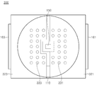
도 1은 본 발명의 제1 실시예에 따른 발광 다이오드를 도시한 사시도이다.
도 2는 도 1의 발광 다이오드를 도시한 평면도이다.
도 3은 도 1의 Ⅰ-Ⅰ'라인을 따라 절단한 발광 다이오드를 도시한 단면도이다.
도 4는 본 발명의 제2 실시예에 따른 발광 다이오드를 도시한 단면도이다.
도 5는 본 발명의 제3 실시예에 따른 발광 다이오드를 도시한 평면도이다.
도 6은 본 발명의 제4 실시예에 따른 발광 다이오드를 도시한 평면도이다.
도 7은 도 6의 Ⅱ-Ⅱ'라인을 따라 절단한 발광 다이오드를 도시한 단면도이다.
도 8은 본 발명의 제5 실시예에 따른 발광 다이오드를 도시한 평면도이다.
도 9는 본 발명의 제6 실시예에 따른 발광 다이오드를 도시한 단면도이다.1 is a perspective view illustrating a light emitting diode according to a first embodiment of the present invention.
2 is a plan view showing the light emitting diode of FIG.
3 is a cross-sectional view illustrating a light emitting diode taken along the line I-I 'of FIG.
4 is a cross-sectional view illustrating a light emitting diode according to a second embodiment of the present invention.
5 is a plan view showing a light emitting diode according to a third embodiment of the present invention.
6 is a plan view showing a light emitting diode according to a fourth embodiment of the present invention.
7 is a cross-sectional view illustrating a light emitting diode taken along line II-II 'of FIG.
8 is a plan view showing a light emitting diode according to a fifth embodiment of the present invention.
9 is a cross-sectional view illustrating a light emitting diode according to a sixth embodiment of the present invention.
이하, 첨부한 도면들을 참조하여 본 발명의 실시예들을 상세히 설명하기로 한다. 다음에 소개되는 실시예들은 당업자에게 본 발명의 사상이 충분히 전달될 수 있도록 하기 위해 예로서 제공되는 것이다. 따라서, 본 발명은 이하 설명되는 실시예들에 한정되지 않고 다른 형태로 구체화될 수도 있다. 그리고, 도면들에 있어서, 구성요소의 폭, 길이, 두께 등은 편의를 위하여 과장되어 표현될 수 있다. 명세서 전체에 걸쳐서 동일한 참조번호들은 동일한 구성요소들을 나타낸다.Hereinafter, embodiments of the present invention will be described in detail with reference to the accompanying drawings. The following embodiments are provided by way of example so that those skilled in the art can fully understand the spirit of the present invention. Therefore, the present invention is not limited to the embodiments described below, but may be embodied in other forms. In the drawings, the width, length, thickness, and the like of the components may be exaggerated for convenience. Like reference numerals designate like elements throughout the specification.
도 1은 본 발명의 제1 실시예에 따른 발광 다이오드를 도시한 사시도이고, 도 2는 도 1의 발광 다이오드를 도시한 평면도이고, 도 3은 도 1의 Ⅰ-Ⅰ'라인을 따라 절단한 발광 다이오드를 도시한 단면도이다.FIG. 1 is a perspective view illustrating a light emitting diode according to a first embodiment of the present invention, FIG. 2 is a plan view illustrating the light emitting diode of FIG. 1, and FIG. 3 is a cross- Sectional view showing a diode.
도 1 내지 도 3에 도시된 바와 같이, 본 발명의 제1 실시예에 따른 발광 다이오드(100)는 기판(110), 제1 및 제2 리드 프레임(121, 123), 서브 마운트 기판(121c), 발광 칩(150), 렌즈(140), 오일(170), 제1 및 제2 차폐부재(161, 163), 제1 및 제2 수용홀(131, 133)을 포함한다.1 to 3, a
상기 서브 마운트 기판(121c)은 상기 제1 및 제2 리드 프레임(121, 123) 형성 시에 동시에 형성된다. 즉, 상기 서브 마운트 기판(121c)은 상기 제1 및 제2 리드 프레임(121, 123)과 동일한 물질로 이루어질 수 있다. 일 예로 상기 서브 마운트 기판(121c)은 도전성 물질로 이루어질 수 있다. 상기 서브 마운트 기판(121c)은 상기 제1 리드 프레임(121)과 연결될 수 있다. 상기 본 발명의 제1 실시예에서는 서브 마운트 기판(121c)과 상기 제1 리드 프레임(121)이 서로 연결된 구조를 한정하여 설명하고 있지만, 이에 한정하지 않고, 상기 서브 마운트 기판(121c)은 상기 제1 리드 프레임(121)으로부터 분리될 수도 있다. 즉, 상기 서브 마운트 기판(121c)은 상기 제1 및 제2 리드 프레임(121, 123)으로부터 분리될 수 있고, 상기 서브 마운트 기판(121c) 상에 실장된 발광 칩(150)은 와이어(미도시)에 의해 상기 제1 및 제2 리드 프레임(121, 123)과 전기적으로 연결될 수 있다.The
상기 발광 칩(150)은 상기 서브 마운트 기판(121c) 상에 실장되며, 전극들(미도시)을 포함한다. 도면에서는 상세히 도시되지 않았지만, 상기 발광 칩(150)은 와이어(미도시)에 의해 상기 제1 및 제2 리드 프레임(121, 123)과 전기적으로 연결될 수 있다. 이에 한정하지 않고, 본 발명의 발광 칩(150)은 상기 발광 칩(150)의 종류에 따라 와이어가 모두 생략되고, 상기 발광 칩(150)의 전극들이 상기 제1 및 제2 리드 프레임(121, 123)과 직접 연결될 수도 있다. 또한, 상기 발광 칩(150)은 전극들 중 어느 하나만 와이어에 의해 상기 제1 및 제2 리드 프레임(121, 123) 중 어느 하나와 연결될 수도 있다.The
상기 기판(110)은 상기 제1 및 제2 리드 프레임(121, 123)의 위치를 결정할 수 있는 기본틀을 제공하고, 상기 서브 마운트 기판(121c)을 지지하는 지지부(111)를 포함한다. 도면에는 상세히 도시되지 않았지만, 상기 지지부(111)는 상기 서브 마운트 기판(121c)과 점착물질을 통해 접착될 수 있다.The
상기 제1 및 제2 리드 프레임(121, 123)은 상기 기판(110)의 외면을 따라 위치하고, 서로 상이한 극성을 가지며, 서로 일정 간격 이격된다. 상기 제1 및 제2 리드 프레임(121, 123)은 발광 칩(150)의 전극들에 각각 접속된다.The first and second lead frames 121 and 123 are located along the outer surface of the
상기 제1 리드 프레임(121)은 상기 기판(110)의 상부면 일부 및 일측면 일부에 위치하는 제1 상부 리드(121a)와, 상기 기판(110)의 하부면 일부 및 일측면 다른 일부에 위치하는 제1 하부 리드(121b)를 포함한다.The
상기 제2 리드 프레임(123)은 상기 기판(110)의 상부면 다른 일부 및 타측면 일부에 위치하는 제2 상부 리드(123a)와, 상기 기판(110)의 하부면 다른 일부 및 타측면 다른 일부에 위치하는 제2 하부 리드(123v)를 포함한다.The
상기 제1 및 제2 수용홀(131, 133)은 상기 기판(110)과 상기 제1 및 제2 리드 프레임(121, 123) 제조시에 형성될 수 있다. 상기 제1 및 제2 수용홀(131, 133)은 상기 기판(110) 내부에 위치할 수 있다. 상기 제1 수용홀(131)은 상기 제1 상부 리드(121a)와 상기 서브 마운트 기판(121c) 사이에 형성될 수 있으며, 상기 제1 하부 리드(121b)를 노출시킨다. 상기 제2 수용홀(133)은 상기 제2 상부 리드(123a)와 상기 서브 마운트 기판(121c) 사이에 형성될 수 있으며, 상기 제2 하부 리드(123b)를 노출시킨다. 따라서, 본 발명의 발광 다이오드(100)는 상기 제1 및 제2 수용홀(131, 133)에 의해서 상기 제1 및 제2 리드 프레임(121, 123)의 내부면 외부로 노출될 수 있다.The first and second receiving
상기 오일(170)은 빛의 투과율이 높은 투광성 물질로 이루어지며, 본 발명에서는 미네랄(mineral) 오일, 아모코(amoco) 오일 중 하나로 이루어질 수 있지만, 이에 한정하지 않고, 모든 가시광 영역에서 투명하고 1.4 내지 1.5의 굴절률을 가지는 오일이라면, 본 발명의 구성으로 사용할 수 있다.The
상기 오일(170)에는 상기 발광 칩(150)으로부터 발생된 광을 사용자가 원하는 특정 파장대의 광으로 변환하는 형광 물질(171)을 포함한다.The
상기 오일(170)은 상기 발광 칩(150) 상에 수용될 뿐만 아니라, 상기 제1 및 제2 수용홀(131, 133)을 통해서 상기 기판(110) 내부에 수용될 수 있다.The
상기 오일(170)은 상기 제1 및 제2 수용홀(131, 133)을 통해서 상기 제1 및 제2 상부 리드(121a, 123a)의 상부면 및 내부면과 접촉될 수 있고, 상기 제1 및 제2 하부 리드(121b, 123b)의 내부면과 접촉될 수 있다. 상기 발광 칩(150) 및 제1 및 제2 리드 프레임(121, 123)으로부터 발생된 열은 오일(170)의 대류에 의해 냉각된다. 본 발명의 발광 다이오드(100)는 상기 오일(170)과, 상기 제1 및 제2 리드 프레임(121, 123)의 접촉 면적을 넓게 함으로써, 대류에 의한 냉각 성능을 극대화할 수 있는 최적화된 구조를 가진다.The
상기 제1 및 제2 차폐 부재(161, 163)는 각각 상기 제1 및 제2 리드 프레임(121, 123)의 외곽에 위치한다. 보다 구체적으로, 상기 제1 차폐 부재(161)는 상기 제1 상부 리드(121a)와 상기 제1 하부 리드(121b)의 경계영역에 형성될 수 있고, 상기 제2 차폐 부재(163)는 상기 제2 상부 리드(123a)와 상기 제2 하부 리드(123b)의 경계영역에 형성될 수 있다. The first and
상기 제1 및 제2 차폐 부재(161, 163)는 상기 기판(110) 내부에 수용된 상기 오일(170)의 누수를 방지하는 기능을 가진다.The first and
또한, 상기 제1 및 제2 차폐 부재(161, 163)는 일정한 탄성을 가진다. 즉, 상기 제1 및 제2 차폐 부재(161, 163)는 탄성을 가지는 수지로 이루어져 열에 의해 오일(170)의 팽창과 수축을 완충하는 기능을 가진다.Also, the first and
상기 제1 및 제2 차폐 부재(161, 163)는 광이 투과될 수 있도록 투광성 수지로 이루어져 발광 다이오드(100)의 측 방향 광 추출을 향상시키는 기능을 가진다.The first and
본 발명의 제1 실시예에서는 제1 및 제2 차폐 부재(161, 163)가 투광성 수지로 한정하여 설명하고 있지만, 이에 한정하지 않고, 비투광성 수지로 이루어질 수도 있다.In the first embodiment of the present invention, the first and
따라서, 본 발명의 발광 다이오드(100)는 상기 제1 및 제2 차폐 부재(161, 163)에 의해서 오일(170)의 팽창과 수축을 완충시켜 제품의 신뢰도를 향상시킬 수 있으며, 측 방향으로의 광 추출을 향상시킬 수 있는 장점을 가진다.Therefore, the
상기 렌즈(140)는 상기 기판(110) 상에 위치하며, 본 실시예에서는 반구 형상으로 한정하여 설명하고 있지만, 이에 한정하지 않고 다양한 형상을 가질 수 있다. 예를 들면, 상면이 평평한 평면형 렌즈도 포함될 수 있다. 상기 렌즈(140)는 별도의 봉지 수지(180)를 통해서 상기 기판(110)과 결합될 수 있다. 이에 한정하지 않고, 렌즈(140)는 별도의 봉합 수지(180)를 사용하지 않고도 기판(110)과 결합될 수도 있다.Although the
본 발명의 제1 실시예에 따른 발광 다이오드(100)의 제조방법은 오일(170)이 수용된 용기에 렌즈(140)가 결합된 기판(110)을 상기 용기에 삽입하여 오일(170)이 상기 기판(110) 내부에 수용되도록 한다. 상기 기판(110) 내부에 오일(170)이 수용되면, 상기 제1 및 제2 차폐 부재(161, 163)를 이용하여 상기 기판(110) 내부의 오일(170)을 차폐한다. 여기서, 상기 렌즈(140)는 용기 내부에서 상기 기판(110)과 결합될 수도 있다.A method of manufacturing a
본 발명의 제1 실시예에 따른 발광 다이오드(100)의 다른 제조방법은 상기 렌즈(140)가 기판(110)과 결합되고, 상기 제1 및 제2 차폐 부재(161, 163)가 설치되기 전에 상기 오일을 상기 제1 또는 제2 차폐 부재(161, 163)가 설치되는 차폐홀을 통해 오일(170)이 주입되는 주입공정으로 제조될 수 있다.Another method of manufacturing the
이상에서와 같이, 본 발명의 제1 실시예에 따른 발광 다이오드(100)는 기판(110)의 내부에 수용된 오일(170)이 제1 및 제2 리드 프레임(121, 123)의 상부면 및 내부면과 직접 접촉되어 대류를 이용한 냉각 성능을 극대화할 수 있다.As described above, the
또한, 본 발명의 제1 실시예에 따른 발광 다이오드(100)는 기판(110)의 외측에 일정한 탄성을 가지며, 투광성 수지로 이루어진 제1 및 제2 차폐 부재(161, 163)가 각각 제1 상부 리드(121a) 및 제1 하부 리드(121b)의 경계영역과, 상기 제2 상부 리드(123a) 및 제2 하부 리드(123b)의 경계영역에 설치되어 오일(170)의 팽창 및 수축을 완충시켜 제품의 신뢰도를 향상시키고, 측 방향 광 효율을 향상시킬 수 있다.The
도 4는 본 발명의 제2 실시예에 따른 발광 다이오드를 도시한 단면도이다.4 is a cross-sectional view illustrating a light emitting diode according to a second embodiment of the present invention.
도 4에 도시된 바와 같이, 본 발명의 제2 실시예에 따른 발광 다이오드(200)는 파장변환층(151), 오일(270), 절연부(113) 및 히트 싱크(280)를 제외한 모든 구성은 상기 본 발명의 제1 실시예에 따른 발광 다이오드(도 1의 100)와 동일하므로 동일한 구성은 동일한 부호를 병기하고, 상세한 설명은 생략하기로 한다.4, the
본 발명의 제2 실시예에 따른 발광 다이오드(200)는 발광 칩(150) 상에 파장변환층(151)이 형성된다.In the
상기 파장변환층(151)은 상기 발광 칩(150)으로부터의 광을 특정 파장대로 변환하는 기능을 가진다. 따라서, 제2 실시예에 따른 발광 다이오드(200)는 상기 파장변환층(151)이 발광 칩(150) 상에 직접 형성되어 상기 오일(170)은 형광 물질을 포함하지 않는다.The
제2 실시예의 발광 다이오드(200)는 발광 칩(150) 상부에 상기 파장변환층(151)이 형성된 구조만을 한정하여 설명하고 있지만, 이에 한정하지 않고, 파장변환층(151)은 발광 칩(150)의 상부 및 측면들을 모두 감싸는 구조로 형성될 수도 있다.The
제2 실시예에 따른 발광 다이오드(200)는 상기 히트 싱크(280)를 더 포함할 수 있다.The
상기 히트 싱크(280)는 서브 마운트 기판(121c)의 하부에 위치하고, 상기 서브 마운트 기판(121c)의 하면과 접촉될 수 있다. 상기 히트 싱크(280)는 열 전도도가 우수하여 상기 서브 마운트 기판(121c)으로부터의 열을 용이하게 배출할 수 있다. 따라서, 상기 히트 싱크(280)는 방열 효과를 더 향상시킬 수 있다.The
상기 절연부(113) 는 기판의 일부분으로 이루어질 수 있다. 상기 절연부(113)는 상기 히트 싱크(280)와 상기 제1 및 제2 리드 프레임(121, 123)을 절연시키는 기능을 가진다. 상기 히트 싱크(280)는 열 전도도가 우수한 금속 물질로 이루어지며, 이에 따라 상기 히트 싱크(280)는 상기 제1 및 제2 리드 프레임(121, 123)과 절연되어야 한다. 따라서, 상기 절연부(113)는 상기 히트 싱크(280)를 감싸는 구조를 가진다The insulating
이상에서와 같이, 본 발명의 제2 실시예에 따른 발광 다이오드(200)는 제1 실시예에 따른 발광 다이오드(도 1의 100)의 효과를 가지며, 발광 칩(150) 상에 형성된 파장변환층(151)에 의해 원하는 파장의 광을 구현함에 있어서, 신뢰성이 보다 더 향상될 수 있으며, 오일(270)에 형광물질을 혼합하는 고정을 생략하여 제조 시간을 줄일 수 있다. 또한, 본 발명의 제2 실시예에 따른 발광 다이오드(200)는 서브 마운트 기판(121c)의 하부에 히트 싱크(280)가 구비되어 방열이 보다 더 우수한 장점을 가진다.As described above, the
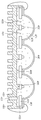
도 5는 본 발명의 제3 실시예에 따른 발광 다이오드를 도시한 평면도이다.5 is a plan view showing a light emitting diode according to a third embodiment of the present invention.
본 발명의 제3 실시예에 따른 발광 다이오드(300)는 제1 및 제2 리드 프레임(321, 323)과, 다수의 제1 및 제2 수용홀(331, 333)을 제외한 모든 구성은 상기 본 발명의 제1 실시예에 따른 발광 다이오드(도 1의 100)와 동일하므로 동일한 구성은 동일한 부호를 병기하고, 상세한 설명은 생략하기로 한다.The
제3 실시예에 따른 발광 다이오드(300)는 발광 칩(150)과 인접한 영역까지 제1 및 제2 리드 프레임(321, 323)이 확장된 구조를 가진다.The
상기 제1 및 제2 리드 프레임(321, 323)은 상기 발광 칩(150)과 인접한 영역까지 확장된 구조에 의해 제1 실시예의 발광 다이오드(도 1의 100) 보다 오일과의 접촉 면적이 넓다. 따라서, 제3 실시예에 따른 발광 다이오드(300)는 방열에 보다 더 우수한 장점을 가진다.The
상기 다수의 제1 및 제2 수용홀(331, 333)은 상기 발광 칩(150)과 인접한 영역까지 확장된 상기 제1 및 제2 리드 프레임(321, 323) 상에 형성될 수 있으며, 상기 제1 및 제2 리드 프레임(321, 323)과 오일의 접촉 면적을 넓히기 위해 원형 타입으로 다수개 형성될 수 있다. 본 발명의 제3 실시예에 따른 발광 다이오드(300)는 상기 다수의 제1 및 제2 수용홀(331, 333)의 형상을 원형 타입으로 한정하고 있지만, 다른 형상으로 변경될 수도 있다.The first and second receiving
도 6은 본 발명의 제4 실시예에 따른 발광 다이오드를 도시한 평면도이고, 도 7은 도 6의 Ⅱ-Ⅱ'라인을 따라 절단한 발광 다이오드를 도시한 단면도이다.FIG. 6 is a plan view illustrating a light emitting diode according to a fourth embodiment of the present invention, and FIG. 7 is a cross-sectional view illustrating a light emitting diode taken along the line II-II 'of FIG.
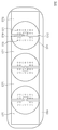
도 6 및 도 7에 도시된 바와 같이, 본 발명의 제4 실시예에 따른 발광 다이오드(400)는 기판(410), 복수의 제1 리드 프레임(421), 복수의 제2 리드 프레임(423), 복수의 발광 칩(450), 복수의 제1 수용홀(431), 복수의 제2 수용홀(433), 렌즈(440) 및 방열 플레이트(490)를 포함한다6 and 7, a
상기 기판(410)은 서로 상이한 극성을 가지는 복수의 제1 및 제2 리드 프레임(421, 423)을 포함한다. 도면에는 상세히 도시되지 않았지만, 상기 기판(410)은 복수의 발광 칩(450)이 실장되는 복수의 서브 마운트 기판을 포함하고, 상기 서브 마운트 기판은 상기 제1 및 제2 리드 프레임(421, 423) 형성 시에 동시에 형성된다.The
상기 복수의 발광 칩(450)은 와이어(미도시)에 의해 상기 제1 및 제2 리드 프레임(421, 423)과 전기적으로 연결될 수 있다. 이에 한정하지 않고, 본 발명의 발광 칩(450)은 상기 발광 칩(450)의 종류에 따라 전극들이 상기 제1 및 제2 리드 프레임(421, 423)과 직접 연결될 수도 있다. 또한, 상기 발광 칩(450)은 전극들 중 하나는 와이어에 의해 상기 제1 및 제2 리드 프레임(421, 423) 중 어느 하나와 연결되고, 다른 하나는 상기 제1 및 제2 리드 프레임(421, 423) 중 다른 하나와 직접 연결 수도 있다.The plurality of
상기 방열 플레이트(490)는 상기 발광 칩(450)과 상응하는 영역이 돌출된 복수의 지지부(495)를 더 포함한다. 상기 지지부(495)는 방열 플레이트(490)의 상부방향으로 돌출되며, 상기 방열 칩(450)의 위치와 상응하는 기판(410)의 하부를 지지한다.The
상기 방열 플레이트(490)의 가장자리에는 상부 방향으로 돌출된 측부를 더 포함한다.The
상기 방열 플레이트(490)는 상기 복수의 지지부(495)와 측부에 의해 음각 형상의 수용홈(493)이 형성될 수 있다.The
상기 방열 플레이트(490)는 상기 하부 방향으로 돌출된 다수의 요철부를 더 포함하고, 상기 요철부는 외부 공기와의 접촉 면적을 넓혀주는 기능을 가진다.The
상기 방열 플레이트(490)는 기판(410) 및 방열 플레이트(490)의 조립 시에 내부에 수용되는 오일(470)에 의한 압력을 조절하기 위해 형성된 관통홀(491)을 더 포함한다.The
본 발명의 제4 실시예의 발광 다이오드(400)는 기판(410)과 렌즈(440) 및 방열 플레이트(490)의 조립을 위해 점착물질(461)이 이용되고, 오일(470)의 누수를 방지하기 위해 상기 기판(410)과 렌즈(440) 및 방열 플레이트(490)의 경계영역을 덮는 제1 봉합 수지(463)가 형성된다.The
또한, 본 발명의 제4 실시예의 발광 다이오드(400)는 상기 관통홀(491)을 봉합하는 제2 봉합 수지(460)를 더 포함할 수 있다.In addition, the
상기 제2 봉합 수지(460)는 기판(410) 및 방열 플레이트(490)에 수용된 상기 오일(470)의 누수를 방지하는 기능을 가진다.The
또한, 상기 제2 봉합 수지(460)는 일정한 탄성을 가진다. 즉, 상기 제2 봉합 수지(460)는 탄성을 가지는 수지로 이루어져 열에 의해 팽창과 수축을 반복하는 오일(470)에 따라 완충 기능을 가진다.In addition, the
상기 복수의 제1 및 제2 수용홀(431, 433)은 상기 기판(410) 제조시에 형성될 수 있다. 상기 제1 및 제2 수용홀(431, 433)은 상기 기판(410)을 관통하여 형성될 수 있다. 상기 복수의 제1 및 제2 수용홀(431, 433)에 의해 상기 방열 플레이트(490)의 내부가 노출될 수 있다.The plurality of first and second receiving
상기 오일(470)은 빛의 투과율이 높은 투광성 물질로 이루어지며, 본 발명에서는 미네랄(mineral) 오일, 아모코(amoco) 오일 중 하나로 이루어질 수 있지만, 이에 한정하지 않고, 모든 가시광 영역에서 투명하고 1.4 내지 1.5의 굴절률을 가지는 오일이라면, 본 발명의 구성으로 사용할 수 있다.The
상기 오일(470)에는 상기 발광 칩(450)으로부터 발생된 광을 사용자가 원하는 특정 파장대의 광으로 변환하는 형광 물질(471)을 포함한다.The
상기 오일(470)은 상기 발광 칩(450) 상에 수용될 뿐만 아니라, 상기 제1 및 제2 수용홀(431, 433)을 통해서 상기 방열 플레이트(490) 내부에 수용될 수 있다.The
상기 오일(470)은 상기 제1 및 제2 수용홀(431, 433)을 통해서 상기 제1 및 제2 리드 프레임(421, 423)과 접촉될 수 있고, 상기 방열 플레이트(490)의 수용홈(495)에 수용될 수 있다. 따라서, 상기 오일(470)은 상기 방열 플레이트(490)의 내부면과 접촉될 수 있다.The
상기 오일(470)은 대류에 의해 상기 발광 칩(450), 제1 및 제2 리드 프레임(421, 423) 및 방열 플레이트(490)와 접촉되어 열을 냉각시킨다. 본 발명의 제4 실시예의 발광 다이오드(400)는 상기 오일(470)과, 상기 방열 플레이트(490), 상기 제1 및 제2 리드 프레임(421, 423)의 접촉 면적을 크게 함으로써, 대류 냉각 성능을 극대화할 수 있는 최적화된 구조를 가진다.The
본 발명의 제4 실시예에 따른 발광 다이오드(400)의 제조방법은 오일(470)이 채워진 용기에서 렌즈(440), 기판(410) 및 방열 플레이트(490)의 조립이 수행된다. 여기서, 상기 렌즈(440), 기판(410) 및 방열 플레이트(490)의 조립은 점착 물질(461)에 의해 이루어질 수 있다.The manufacturing method of the
여기서, 상기 기판(410)과 방열 플레이트(490)의 지지부(493)는 방열기능을 향상시키기 위해 전도성 테이프 등으로 서로 접착될 수 있다.Here, the
상기 오일(470)이 수용된 용기 내에서 상기 렌즈(440), 기판(410) 및 방열 플레이트(490)의 조립이 완료되면, 오일(470)의 누수를 방지하기 위해 제1 봉합 수지(463)를 이용하여 상기 기판(410)과 렌즈(440) 및 방열 플레이트(490)의 경계영역을 덮는다.When the assembly of the
여기서, 본 발명의 제4 실시예의 발광 다이오드(400)는 상기 제1 봉합 수지(463)를 덮기 전에 상기 제2 봉합 수지(460)를 이용하여 상기 관통홀(491)을 봉합할 수 있다.Here, the
이상에서와 같이, 본 발명의 제4 실시예에 따른 발광 다이오드(400)는 오일(470)이 기판(410)의 제1 및 제2 수용홀(461, 433)을 통해서 방열 플레이트(490)의 수용홈(495)으로 수용되어 대류를 이용한 냉각 성능을 극대화할 수 있다.As described above, in the
또한, 본 발명의 제4 실시예에 따른 발광 다이오드(400)는 오일(470)의 팽창 및 수축을 완충시킬 수 있는 제2 봉합 수지(460)가 구비되어 제품의 신뢰도를 향상시킬 수 있다.In addition, the
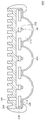
도 8은 본 발명의 제5 실시예에 따른 발광 다이오드를 도시한 평면도이고, 도 9는 본 발명의 제6 실시예에 따른 발광 다이오드를 도시한 단면도이다.FIG. 8 is a plan view illustrating a light emitting diode according to a fifth embodiment of the present invention, and FIG. 9 is a cross-sectional view illustrating a light emitting diode according to a sixth embodiment of the present invention.
도 8에 도시된 바와 같이, 본 발명의 제5 실시예에 따른 발광 다이오드(500)는 기판(510), 다수의 제1 및 제2 수용홀(531, 533), 제1 및 제2 리드 프레임(521, 523)을 제외한 모든 구성은 상기 본 발명의 제4 실시예에 따른 발광 다이오드(도 6의 400)와 동일함으로 동일한 구성은 동일한 부호를 병기하고, 상세한 설명은 생략하기로 한다.8, a
상기 제1 및 제2 리드 프레임(521, 523)은 상기 발광 칩(450)과 인접한 영역까지 확장된 구조를 가진다. 따라서, 제5 실시예에 따른 발광 다이오드(500)는 제4 실시예의 발광 다이오드(도 6의 400) 보다 오일과의 접촉 면적이 크다. 제5 실시예의 발광 다이오드(500)는 방열이 보다 더 우수한 장점을 가진다.The first and second lead frames 521 and 523 are extended to a region adjacent to the
상기 다수의 제1 및 제2 수용홀(531, 533)은 상기 발광 칩(450)과 인접한 영역까지 확장된 상기 제1 및 제2 리드 프레임(521, 523) 상에 형성될 수 있으며, 상기 제1 및 제2 리드 프레임(521, 523)과 오일의 접촉 면적을 넓히기 위해 원형 타입으로 다수개 형성될 수 있다. 본 발명의 제5 실시예에 따른 발광 다이오드(500)는 상기 다수의 제1 및 제2 수용홀(531, 533)의 형상을 원형 타입으로 한정하고 있지만, 다른 형상으로 변경될 수 있다.The plurality of first and second receiving
도 9에 도시된 바와 같이, 본 발명의 제6 실시예에 따른 발광 다이오드(600)는 파장변환층(651) 및 오일(670)을 제외한 모든 구성은 상기 본 발명의 제4 실시예에 따른 발광 다이오드(도 6의 400)와 동일함으로 동일한 구성은 동일한 부호를 병기하고, 상세한 설명은 생략하기로 한다.9, in the
본 발명의 제6 실시예에 따른 발광 다이오드(600)는 발광 칩(650) 상에 파장편환층(651)이 형성된다.In the
상기 파장변환층(651)은 상기 발광 칩(650)으로부터의 광을 특정 파장대로 변환하는 기능을 가진다. 따라서, 제6 실시예에 따른 발광 다이오드(600)는 상기 파장변환층(651)이 발광 칩(650) 상에 직접 형성되어 상기 오일(670)은 형광 물질을 포함하지 않는다.The
제6 실시예의 발광 다이오드(600)는 발광 칩(650) 상부에 상기 파장변환층(651)이 형성된 구조만을 한정하여 설명하고 있지만, 이에 한정하지 않고, 파장변환층(651)은 발광 칩(650)의 상부 및 측면들을 모두 감싸는 구조로 형성될 수도 있다.The
이상에서와 같이, 본 발명의 제6 실시예의 발광 다이오드(60)는 제4 실시예에 따른 발광 다이오드(도 6의 400)의 효과를 가지며, 발광 칩(650) 상에 형성된 파장변환층(651)에 의해 원하는 파장의 광을 구현함에 있어서, 신뢰성이 보다 더 향상될 수 있으며, 오일(670)에 형광물질을 혼합하는 고정을 생략하여 제조 시간을 줄일 수 있는 장점을 가진다.As described above, the light emitting diode 60 of the sixth embodiment of the present invention has the effect of the light emitting diode (400 of FIG. 6) according to the fourth embodiment, and the
이상에서는 복수의 발광 칩(650)이 일방향으로 복수개로 구비된 1열 구조를 한정하여 설명하고 있지만, 이에 한정하지 않고, 복수의 열을 가질 수 있다. 즉, 본 발명의 발광 다이오드는 발광 칩의 배열 구조에 있어서, 복수의 열과 복수의 행으로 배열되는 다양한 배열 구조를 모두 포함할 수 있다.In the above description, the one-column structure in which the plurality of
또한, 본 발명의 발광 칩은 베이스 기판으로 사파이어 기판, 스피넬 기판, 질화갈륨 기판, 탄화실리콘 기판 또는 실리콘 기판이 이용될 수 있다. 본 발명에서는 성장되는 반도체층과의 결정결함을 줄여 고효율의 발광 다이오드를 구현할 수 있도록 베이스 기판으로 질화갈륨 기판을 사용할 수 있다.In addition, a sapphire substrate, a spinel substrate, a gallium nitride substrate, a silicon carbide substrate, or a silicon substrate may be used as the base substrate of the light emitting chip of the present invention. In the present invention, a gallium nitride substrate can be used as a base substrate so as to realize a high-efficiency light emitting diode by reducing crystal defects with a semiconductor layer to be grown.
또한, 본 발명의 발광 다이오드는 오일에 형광 물질이 포함되거나, 발광 칩 상에 파장변환층이 직접 형성되는 실시예들을 한정하여 설명하고 있지만, 이에 한정하지 않고, 렌즈의 내부면 또는 외부면 상에 형광물질이 도포된 발광 다이오드 및 렌즈 내부에 형광물질이 포함된 발광 다이오드도 모두 포함될 수 있다.In addition, the light emitting diode of the present invention is limited to the embodiments in which the fluorescent material is contained in the oil or the wavelength conversion layer is directly formed on the light emitting chip. However, the present invention is not limited to this, A light emitting diode coated with a fluorescent material and a light emitting diode including a fluorescent material inside the lens may all be included.
이상에서, 본 발명의 다양한 실시예들 및 특징들에 대해 설명하였지만, 본 발명은 위에서 설명한 실시예들 및 특징들에 한정되는 것은 아니며, 본 발명의 사상을 벗어나지 않는 범위 내에서 다양하게 변형될 수 있다.While the present invention has been particularly shown and described with reference to exemplary embodiments thereof, it is to be understood that the invention is not limited to the disclosed exemplary embodiments or constructions. Various changes and modifications may be made without departing from the spirit and scope of the invention. have.
131, 331, 431, 531 : 제1 수용홀 133, 333, 433, 533 : 제2 수용홀
161 : 제1 차폐 부재 163 : 제2 차폐 부재
280 : 히트 싱크 460 : 제2 봉합 수지
463 : 제1 봉합 수지 490 : 방열 플레이트
495 : 수용홈 491 : 관통홀131, 331, 431, 531: first receiving
161: first shielding member 163: second shielding member
280: Heat sink 460: Second sealing resin
463: first sealing resin 490: heat dissipating plate
495: receiving groove 491: through hole
Claims (21)
상기 발광 칩의 전극들과 전기적으로 접속되는 리드 프레임을 포함하는 기판;
상기 기판상에 위치하여 상기 발광 칩을 감싸는 렌즈; 및
상기 렌즈의 내부 및 상기 기판의 내부에 수용된 오일을 포함하는 발광 다이오드.At least one light emitting chip;
A substrate including a lead frame electrically connected to the electrodes of the light emitting chip;
A lens positioned on the substrate and surrounding the light emitting chip; And
And an oil accommodated inside the lens and inside the substrate.
상기 제2 봉합 수지는 투광성 수지로 이루어지고, 일정한 탄성을 가지는 발광 다이오드.[12] The method of claim 12, further comprising a second sealing resin for sealing the through hole,
And the second sealing resin is made of a light transmitting resin and has a constant elasticity.
상기 오일이 채워진 용기에 적어도 하나 이상의 발광 칩이 실장된 상기 기판 및 상기 발광 칩을 덮는 상기 렌즈를 삽입하여 오일을 수용하는 단계; 및
탄성을 가지는 수지를 이용하여 상기 기판 내의 상기 오일을 차폐하는 단계를 포함하는 발광 다이오드의 제조방법.A method of manufacturing a light emitting diode in which oil is contained in a lens and in a substrate,
Receiving the oil by inserting the substrate on which the at least one light emitting chip is mounted and the lens covering the light emitting chip in a container filled with the oil; And
And shielding the oil in the substrate using a resin having elasticity.
[20] The method of claim 19, wherein the step of shielding the oil includes sealing the through hole located in the lower portion of the heat dissipation plate.
Priority Applications (3)
| Application Number | Priority Date | Filing Date | Title |
|---|---|---|---|
| KR1020120138057A KR20140070045A (en) | 2012-11-30 | 2012-11-30 | Light emitting diode and method of fabricating the same |
| PCT/KR2013/011057 WO2014084693A1 (en) | 2012-11-30 | 2013-12-02 | Light-emitting diode, and method for manufacturing same |
| US14/648,805 US9640745B2 (en) | 2012-11-30 | 2013-12-02 | Light emitting diode and method of manufacturing the same |
Applications Claiming Priority (1)
| Application Number | Priority Date | Filing Date | Title |
|---|---|---|---|
| KR1020120138057A KR20140070045A (en) | 2012-11-30 | 2012-11-30 | Light emitting diode and method of fabricating the same |
Publications (1)
| Publication Number | Publication Date |
|---|---|
| KR20140070045A true KR20140070045A (en) | 2014-06-10 |
Family
ID=50828230
Family Applications (1)
| Application Number | Title | Priority Date | Filing Date |
|---|---|---|---|
| KR1020120138057A KR20140070045A (en) | 2012-11-30 | 2012-11-30 | Light emitting diode and method of fabricating the same |
Country Status (3)
| Country | Link |
|---|---|
| US (1) | US9640745B2 (en) |
| KR (1) | KR20140070045A (en) |
| WO (1) | WO2014084693A1 (en) |
Families Citing this family (4)
| Publication number | Priority date | Publication date | Assignee | Title |
|---|---|---|---|---|
| CN104362247A (en) * | 2014-11-06 | 2015-02-18 | 中国科学院广州能源研究所 | LED light-emitting module applicable to fluid heat transfer |
| US10403792B2 (en) * | 2016-03-07 | 2019-09-03 | Rayvio Corporation | Package for ultraviolet emitting devices |
| JP1655194S (en) * | 2019-06-04 | 2020-03-16 | ||
| JP1655195S (en) * | 2019-06-04 | 2020-03-16 |
Family Cites Families (21)
| Publication number | Priority date | Publication date | Assignee | Title |
|---|---|---|---|---|
| JP3700482B2 (en) * | 1999-07-23 | 2005-09-28 | 松下電工株式会社 | Light source device |
| JP3614776B2 (en) * | 2000-12-19 | 2005-01-26 | シャープ株式会社 | Chip component type LED and its manufacturing method |
| US20040264192A1 (en) * | 2003-05-06 | 2004-12-30 | Seiko Epson Corporation | Light source apparatus, method of manufacture therefor, and projection-type display apparatus |
| DE102004063978B4 (en) * | 2003-07-17 | 2019-01-24 | Toyoda Gosei Co., Ltd. | Light-emitting device |
| JP2005079149A (en) * | 2003-08-28 | 2005-03-24 | Seiko Epson Corp | Light source unit and projector |
| TWI257718B (en) * | 2004-03-18 | 2006-07-01 | Phoseon Technology Inc | Direct cooling of LEDs |
| US7560820B2 (en) * | 2004-04-15 | 2009-07-14 | Saes Getters S.P.A. | Integrated getter for vacuum or inert gas packaged LEDs |
| US7737634B2 (en) * | 2006-03-06 | 2010-06-15 | Avago Technologies General Ip (Singapore) Pte. Ltd. | LED devices having improved containment for liquid encapsulant |
| DE102006015606A1 (en) * | 2006-04-04 | 2007-10-18 | Noctron Holding S.A. | Semiconductor lamps and light panels with such |
| KR20080032882A (en) * | 2006-10-11 | 2008-04-16 | 삼성전기주식회사 | Light emitting diode package |
| WO2008055616A1 (en) * | 2006-11-07 | 2008-05-15 | Perkinelmer Optoelectronics Gmbh & Co. Kg | Method for bonding metal surfaces by applying a first oxidised metal layer and a second oxidised metal layer object having cavities or structure of a light emitting diode produced through the last method |
| JP2008122499A (en) * | 2006-11-09 | 2008-05-29 | Sony Corp | Surface light source device and liquid crystal display assembly |
| JP4924053B2 (en) * | 2007-01-19 | 2012-04-25 | カシオ計算機株式会社 | Light emitting device and printing device |
| US20090001372A1 (en) * | 2007-06-29 | 2009-01-01 | Lumination Llc | Efficient cooling of lasers, LEDs and photonics devices |
| US20090126922A1 (en) | 2007-10-29 | 2009-05-21 | Jan Vetrovec | Heat transfer device |
| US20090140271A1 (en) * | 2007-11-30 | 2009-06-04 | Wen-Jyh Sah | Light emitting unit |
| KR100929325B1 (en) * | 2007-12-31 | 2009-11-27 | 서울반도체 주식회사 | Heat dissipation LED package |
| TW201007091A (en) * | 2008-05-08 | 2010-02-16 | Lok F Gmbh | Lamp device |
| US8390193B2 (en) * | 2008-12-31 | 2013-03-05 | Intematix Corporation | Light emitting device with phosphor wavelength conversion |
| TWI436506B (en) * | 2011-04-20 | 2014-05-01 | Lustrous Green Technology Of Lighting | Led package structure using a prefabricated phosphor cap |
| JP5893874B2 (en) * | 2011-09-02 | 2016-03-23 | 信越化学工業株式会社 | Optical semiconductor device |
-
2012
- 2012-11-30 KR KR1020120138057A patent/KR20140070045A/en not_active Application Discontinuation
-
2013
- 2013-12-02 US US14/648,805 patent/US9640745B2/en not_active Expired - Fee Related
- 2013-12-02 WO PCT/KR2013/011057 patent/WO2014084693A1/en active Application Filing
Also Published As
| Publication number | Publication date |
|---|---|
| WO2014084693A1 (en) | 2014-06-05 |
| US20150340581A1 (en) | 2015-11-26 |
| US9640745B2 (en) | 2017-05-02 |
Similar Documents
| Publication | Publication Date | Title |
|---|---|---|
| CN101051665B (en) | Light emitting diode package having anodized insulation layer and fabrication method therefor | |
| US8067782B2 (en) | LED package and light source device using same | |
| US7923739B2 (en) | Solid state lighting device | |
| US8158996B2 (en) | Semiconductor light emitting device package | |
| TWI542039B (en) | Light emitting diode package and carrier | |
| TWI620304B (en) | Led module | |
| US20150003038A1 (en) | Led assembly with omnidirectional light field | |
| KR20080030584A (en) | Package structure of semiconductor light-emitting device | |
| JP2010129615A (en) | Light emitting device, and illuminating apparatus | |
| KR101055074B1 (en) | Light emitting device | |
| WO2005083804A1 (en) | Light emitting diode with integral heat dissipation means | |
| JP2007043126A (en) | Luminaire using led | |
| US7923271B1 (en) | Method of assembling multi-layer LED array engine | |
| KR20140070045A (en) | Light emitting diode and method of fabricating the same | |
| US9822959B2 (en) | Light emitting device | |
| KR100780236B1 (en) | Light emitting diode package | |
| US9429305B2 (en) | Light emitting device | |
| TW201407748A (en) | LED light bar | |
| JP6210720B2 (en) | LED package | |
| KR20120001189A (en) | Light emitting diode package | |
| JP4678389B2 (en) | Light emitting device | |
| KR101468961B1 (en) | Light emitting device and backlight unit comprising the same | |
| KR100878398B1 (en) | High power led package and fabrication method thereof | |
| KR101152173B1 (en) | LED Package and Method of manufacturing LED Package | |
| TWI440207B (en) | The light emitting diode element is equipped with a light source |
Legal Events
| Date | Code | Title | Description |
|---|---|---|---|
| WITN | Application deemed withdrawn, e.g. because no request for examination was filed or no examination fee was paid |