KR20140065407A - Process for producing metallic particle assembly - Google Patents
Process for producing metallic particle assembly Download PDFInfo
- Publication number
- KR20140065407A KR20140065407A KR1020147005981A KR20147005981A KR20140065407A KR 20140065407 A KR20140065407 A KR 20140065407A KR 1020147005981 A KR1020147005981 A KR 1020147005981A KR 20147005981 A KR20147005981 A KR 20147005981A KR 20140065407 A KR20140065407 A KR 20140065407A
- Authority
- KR
- South Korea
- Prior art keywords
- metal
- aggregate
- particles
- average
- range
- Prior art date
Links
- 238000000034 method Methods 0.000 title claims description 32
- 230000008569 process Effects 0.000 title description 6
- 239000013528 metallic particle Substances 0.000 title description 3
- 239000002245 particle Substances 0.000 claims abstract description 476
- 229910052751 metal Inorganic materials 0.000 claims abstract description 425
- 239000002184 metal Substances 0.000 claims abstract description 425
- 239000000758 substrate Substances 0.000 claims abstract description 116
- 238000004519 manufacturing process Methods 0.000 claims abstract description 32
- 229910052709 silver Inorganic materials 0.000 claims description 51
- 239000004332 silver Substances 0.000 claims description 51
- 238000000862 absorption spectrum Methods 0.000 claims description 50
- 239000000463 material Substances 0.000 claims description 47
- 239000002923 metal particle Substances 0.000 claims description 43
- 238000002835 absorbance Methods 0.000 claims description 31
- 238000004544 sputter deposition Methods 0.000 claims description 15
- XKRFYHLGVUSROY-UHFFFAOYSA-N argon Substances [Ar] XKRFYHLGVUSROY-UHFFFAOYSA-N 0.000 claims description 6
- 229910000510 noble metal Inorganic materials 0.000 claims description 6
- 229910052786 argon Inorganic materials 0.000 claims description 5
- 239000004065 semiconductor Substances 0.000 claims 1
- 239000010409 thin film Substances 0.000 description 121
- 230000000052 comparative effect Effects 0.000 description 96
- BQCADISMDOOEFD-UHFFFAOYSA-N Silver Chemical compound [Ag] BQCADISMDOOEFD-UHFFFAOYSA-N 0.000 description 56
- WZFUQSJFWNHZHM-UHFFFAOYSA-N 2-[4-[2-(2,3-dihydro-1H-inden-2-ylamino)pyrimidin-5-yl]piperazin-1-yl]-1-(2,4,6,7-tetrahydrotriazolo[4,5-c]pyridin-5-yl)ethanone Chemical compound C1C(CC2=CC=CC=C12)NC1=NC=C(C=N1)N1CCN(CC1)CC(=O)N1CC2=C(CC1)NN=N2 WZFUQSJFWNHZHM-UHFFFAOYSA-N 0.000 description 35
- 230000002708 enhancing effect Effects 0.000 description 33
- 239000011521 glass Substances 0.000 description 33
- 238000006243 chemical reaction Methods 0.000 description 28
- 230000000694 effects Effects 0.000 description 28
- 239000000243 solution Substances 0.000 description 27
- 230000003287 optical effect Effects 0.000 description 25
- 239000010408 film Substances 0.000 description 24
- ZYGHJZDHTFUPRJ-UHFFFAOYSA-N coumarin Chemical compound C1=CC=C2OC(=O)C=CC2=C1 ZYGHJZDHTFUPRJ-UHFFFAOYSA-N 0.000 description 22
- LFQSCWFLJHTTHZ-UHFFFAOYSA-N Ethanol Chemical compound CCO LFQSCWFLJHTTHZ-UHFFFAOYSA-N 0.000 description 20
- CDBYLPFSWZWCQE-UHFFFAOYSA-L Sodium Carbonate Chemical compound [Na+].[Na+].[O-]C([O-])=O CDBYLPFSWZWCQE-UHFFFAOYSA-L 0.000 description 19
- 230000001443 photoexcitation Effects 0.000 description 17
- 239000002082 metal nanoparticle Substances 0.000 description 16
- OHVLMTFVQDZYHP-UHFFFAOYSA-N 1-(2,4,6,7-tetrahydrotriazolo[4,5-c]pyridin-5-yl)-2-[4-[2-[[3-(trifluoromethoxy)phenyl]methylamino]pyrimidin-5-yl]piperazin-1-yl]ethanone Chemical compound N1N=NC=2CN(CCC=21)C(CN1CCN(CC1)C=1C=NC(=NC=1)NCC1=CC(=CC=C1)OC(F)(F)F)=O OHVLMTFVQDZYHP-UHFFFAOYSA-N 0.000 description 15
- 238000001878 scanning electron micrograph Methods 0.000 description 15
- 238000004020 luminiscence type Methods 0.000 description 14
- 238000000089 atomic force micrograph Methods 0.000 description 13
- 230000003993 interaction Effects 0.000 description 13
- 238000005259 measurement Methods 0.000 description 13
- 230000009471 action Effects 0.000 description 11
- 229960000956 coumarin Drugs 0.000 description 11
- 235000001671 coumarin Nutrition 0.000 description 11
- 230000005284 excitation Effects 0.000 description 11
- WWSJZGAPAVMETJ-UHFFFAOYSA-N 2-[4-[2-(2,3-dihydro-1H-inden-2-ylamino)pyrimidin-5-yl]-3-ethoxypyrazol-1-yl]-1-(2,4,6,7-tetrahydrotriazolo[4,5-c]pyridin-5-yl)ethanone Chemical compound C1C(CC2=CC=CC=C12)NC1=NC=C(C=N1)C=1C(=NN(C=1)CC(=O)N1CC2=C(CC1)NN=N2)OCC WWSJZGAPAVMETJ-UHFFFAOYSA-N 0.000 description 10
- 239000007769 metal material Substances 0.000 description 10
- 230000001965 increasing effect Effects 0.000 description 8
- 238000002347 injection Methods 0.000 description 8
- 239000007924 injection Substances 0.000 description 8
- 238000000691 measurement method Methods 0.000 description 8
- 238000000295 emission spectrum Methods 0.000 description 7
- 239000002105 nanoparticle Substances 0.000 description 7
- 238000000870 ultraviolet spectroscopy Methods 0.000 description 7
- KZEVSDGEBAJOTK-UHFFFAOYSA-N 1-(2,4,6,7-tetrahydrotriazolo[4,5-c]pyridin-5-yl)-2-[5-[2-[[3-(trifluoromethoxy)phenyl]methylamino]pyrimidin-5-yl]-1,3,4-oxadiazol-2-yl]ethanone Chemical compound N1N=NC=2CN(CCC=21)C(CC=1OC(=NN=1)C=1C=NC(=NC=1)NCC1=CC(=CC=C1)OC(F)(F)F)=O KZEVSDGEBAJOTK-UHFFFAOYSA-N 0.000 description 6
- YJLUBHOZZTYQIP-UHFFFAOYSA-N 2-[5-[2-(2,3-dihydro-1H-inden-2-ylamino)pyrimidin-5-yl]-1,3,4-oxadiazol-2-yl]-1-(2,4,6,7-tetrahydrotriazolo[4,5-c]pyridin-5-yl)ethanone Chemical compound C1C(CC2=CC=CC=C12)NC1=NC=C(C=N1)C1=NN=C(O1)CC(=O)N1CC2=C(CC1)NN=N2 YJLUBHOZZTYQIP-UHFFFAOYSA-N 0.000 description 6
- CONKBQPVFMXDOV-QHCPKHFHSA-N 6-[(5S)-5-[[4-[2-(2,3-dihydro-1H-inden-2-ylamino)pyrimidin-5-yl]piperazin-1-yl]methyl]-2-oxo-1,3-oxazolidin-3-yl]-3H-1,3-benzoxazol-2-one Chemical compound C1C(CC2=CC=CC=C12)NC1=NC=C(C=N1)N1CCN(CC1)C[C@H]1CN(C(O1)=O)C1=CC2=C(NC(O2)=O)C=C1 CONKBQPVFMXDOV-QHCPKHFHSA-N 0.000 description 6
- 239000011248 coating agent Substances 0.000 description 6
- 238000000576 coating method Methods 0.000 description 6
- 239000003574 free electron Substances 0.000 description 6
- 230000007246 mechanism Effects 0.000 description 6
- FOIXSVOLVBLSDH-UHFFFAOYSA-N Silver ion Chemical compound [Ag+] FOIXSVOLVBLSDH-UHFFFAOYSA-N 0.000 description 5
- -1 argon ion Chemical class 0.000 description 5
- 238000001228 spectrum Methods 0.000 description 5
- 238000004528 spin coating Methods 0.000 description 5
- VWVRASTUFJRTHW-UHFFFAOYSA-N 2-[3-(azetidin-3-yloxy)-4-[2-(2,3-dihydro-1H-inden-2-ylamino)pyrimidin-5-yl]pyrazol-1-yl]-1-(2,4,6,7-tetrahydrotriazolo[4,5-c]pyridin-5-yl)ethanone Chemical compound O=C(CN1C=C(C(OC2CNC2)=N1)C1=CN=C(NC2CC3=C(C2)C=CC=C3)N=C1)N1CCC2=C(C1)N=NN2 VWVRASTUFJRTHW-UHFFFAOYSA-N 0.000 description 4
- JQMFQLVAJGZSQS-UHFFFAOYSA-N 2-[4-[2-(2,3-dihydro-1H-inden-2-ylamino)pyrimidin-5-yl]piperazin-1-yl]-N-(2-oxo-3H-1,3-benzoxazol-6-yl)acetamide Chemical compound C1C(CC2=CC=CC=C12)NC1=NC=C(C=N1)N1CCN(CC1)CC(=O)NC1=CC2=C(NC(O2)=O)C=C1 JQMFQLVAJGZSQS-UHFFFAOYSA-N 0.000 description 4
- CSCPPACGZOOCGX-UHFFFAOYSA-N Acetone Chemical compound CC(C)=O CSCPPACGZOOCGX-UHFFFAOYSA-N 0.000 description 4
- KDLHZDBZIXYQEI-UHFFFAOYSA-N Palladium Chemical compound [Pd] KDLHZDBZIXYQEI-UHFFFAOYSA-N 0.000 description 4
- 238000010521 absorption reaction Methods 0.000 description 4
- 238000000151 deposition Methods 0.000 description 4
- 230000008021 deposition Effects 0.000 description 4
- 230000001678 irradiating effect Effects 0.000 description 4
- 238000001748 luminescence spectrum Methods 0.000 description 4
- BASFCYQUMIYNBI-UHFFFAOYSA-N platinum Chemical compound [Pt] BASFCYQUMIYNBI-UHFFFAOYSA-N 0.000 description 4
- 229920000642 polymer Polymers 0.000 description 4
- 238000001771 vacuum deposition Methods 0.000 description 4
- SECXISVLQFMRJM-UHFFFAOYSA-N N-Methylpyrrolidone Chemical compound CN1CCCC1=O SECXISVLQFMRJM-UHFFFAOYSA-N 0.000 description 3
- 239000006185 dispersion Substances 0.000 description 3
- 230000002779 inactivation Effects 0.000 description 3
- 150000002500 ions Chemical class 0.000 description 3
- 230000031700 light absorption Effects 0.000 description 3
- 239000007788 liquid Substances 0.000 description 3
- 239000011159 matrix material Substances 0.000 description 3
- TVIVIEFSHFOWTE-UHFFFAOYSA-K tri(quinolin-8-yloxy)alumane Chemical compound [Al+3].C1=CN=C2C([O-])=CC=CC2=C1.C1=CN=C2C([O-])=CC=CC2=C1.C1=CN=C2C([O-])=CC=CC2=C1 TVIVIEFSHFOWTE-UHFFFAOYSA-K 0.000 description 3
- XLYOFNOQVPJJNP-UHFFFAOYSA-N water Substances O XLYOFNOQVPJJNP-UHFFFAOYSA-N 0.000 description 3
- IHCCLXNEEPMSIO-UHFFFAOYSA-N 2-[4-[2-(2,3-dihydro-1H-inden-2-ylamino)pyrimidin-5-yl]piperidin-1-yl]-1-(2,4,6,7-tetrahydrotriazolo[4,5-c]pyridin-5-yl)ethanone Chemical compound C1C(CC2=CC=CC=C12)NC1=NC=C(C=N1)C1CCN(CC1)CC(=O)N1CC2=C(CC1)NN=N2 IHCCLXNEEPMSIO-UHFFFAOYSA-N 0.000 description 2
- JVKRKMWZYMKVTQ-UHFFFAOYSA-N 2-[4-[2-(2,3-dihydro-1H-inden-2-ylamino)pyrimidin-5-yl]pyrazol-1-yl]-N-(2-oxo-3H-1,3-benzoxazol-6-yl)acetamide Chemical compound C1C(CC2=CC=CC=C12)NC1=NC=C(C=N1)C=1C=NN(C=1)CC(=O)NC1=CC2=C(NC(O2)=O)C=C1 JVKRKMWZYMKVTQ-UHFFFAOYSA-N 0.000 description 2
- NRZJOTSUPLCYDJ-UHFFFAOYSA-N 7-(ethylamino)-6-methyl-4-(trifluoromethyl)chromen-2-one Chemical compound O1C(=O)C=C(C(F)(F)F)C2=C1C=C(NCC)C(C)=C2 NRZJOTSUPLCYDJ-UHFFFAOYSA-N 0.000 description 2
- HEDRZPFGACZZDS-UHFFFAOYSA-N Chloroform Chemical compound ClC(Cl)Cl HEDRZPFGACZZDS-UHFFFAOYSA-N 0.000 description 2
- RYGMFSIKBFXOCR-UHFFFAOYSA-N Copper Chemical compound [Cu] RYGMFSIKBFXOCR-UHFFFAOYSA-N 0.000 description 2
- 229910004298 SiO 2 Inorganic materials 0.000 description 2
- 230000015572 biosynthetic process Effects 0.000 description 2
- MVPPADPHJFYWMZ-UHFFFAOYSA-N chlorobenzene Chemical compound ClC1=CC=CC=C1 MVPPADPHJFYWMZ-UHFFFAOYSA-N 0.000 description 2
- 239000000470 constituent Substances 0.000 description 2
- 229910052802 copper Inorganic materials 0.000 description 2
- 239000010949 copper Substances 0.000 description 2
- 230000005684 electric field Effects 0.000 description 2
- 239000008393 encapsulating agent Substances 0.000 description 2
- 238000005516 engineering process Methods 0.000 description 2
- 238000011156 evaluation Methods 0.000 description 2
- 239000007789 gas Substances 0.000 description 2
- PCHJSUWPFVWCPO-UHFFFAOYSA-N gold Chemical compound [Au] PCHJSUWPFVWCPO-UHFFFAOYSA-N 0.000 description 2
- 229910052737 gold Inorganic materials 0.000 description 2
- 239000010931 gold Substances 0.000 description 2
- 239000010445 mica Substances 0.000 description 2
- 229910052618 mica group Inorganic materials 0.000 description 2
- 239000003960 organic solvent Substances 0.000 description 2
- 229910052763 palladium Inorganic materials 0.000 description 2
- 229910052697 platinum Inorganic materials 0.000 description 2
- 238000002360 preparation method Methods 0.000 description 2
- MUSLHCJRTRQOSP-UHFFFAOYSA-N rhodamine 101 Chemical compound [O-]C(=O)C1=CC=CC=C1C(C1=CC=2CCCN3CCCC(C=23)=C1O1)=C2C1=C(CCC1)C3=[N+]1CCCC3=C2 MUSLHCJRTRQOSP-UHFFFAOYSA-N 0.000 description 2
- 239000002904 solvent Substances 0.000 description 2
- 239000000126 substance Substances 0.000 description 2
- 238000012546 transfer Methods 0.000 description 2
- 238000007740 vapor deposition Methods 0.000 description 2
- JNGRENQDBKMCCR-UHFFFAOYSA-N 2-(3-amino-6-iminoxanthen-9-yl)benzoic acid;hydrochloride Chemical compound [Cl-].C=12C=CC(=[NH2+])C=C2OC2=CC(N)=CC=C2C=1C1=CC=CC=C1C(O)=O JNGRENQDBKMCCR-UHFFFAOYSA-N 0.000 description 1
- HVTQDSGGHBWVTR-UHFFFAOYSA-N 2-[4-[2-(2,3-dihydro-1H-inden-2-ylamino)pyrimidin-5-yl]-3-phenylmethoxypyrazol-1-yl]-1-morpholin-4-ylethanone Chemical compound C(C1=CC=CC=C1)OC1=NN(C=C1C=1C=NC(=NC=1)NC1CC2=CC=CC=C2C1)CC(=O)N1CCOCC1 HVTQDSGGHBWVTR-UHFFFAOYSA-N 0.000 description 1
- ZRPAUEVGEGEPFQ-UHFFFAOYSA-N 2-[4-[2-(2,3-dihydro-1H-inden-2-ylamino)pyrimidin-5-yl]pyrazol-1-yl]-1-(2,4,6,7-tetrahydrotriazolo[4,5-c]pyridin-5-yl)ethanone Chemical compound C1C(CC2=CC=CC=C12)NC1=NC=C(C=N1)C=1C=NN(C=1)CC(=O)N1CC2=C(CC1)NN=N2 ZRPAUEVGEGEPFQ-UHFFFAOYSA-N 0.000 description 1
- MGGVALXERJRIRO-UHFFFAOYSA-N 4-[2-(2,3-dihydro-1H-inden-2-ylamino)pyrimidin-5-yl]-2-[2-oxo-2-(2,4,6,7-tetrahydrotriazolo[4,5-c]pyridin-5-yl)ethyl]-1H-pyrazol-5-one Chemical compound C1C(CC2=CC=CC=C12)NC1=NC=C(C=N1)C=1C(=NN(C=1)CC(=O)N1CC2=C(CC1)NN=N2)O MGGVALXERJRIRO-UHFFFAOYSA-N 0.000 description 1
- WTFUTSCZYYCBAY-SXBRIOAWSA-N 6-[(E)-C-[[4-[2-(2,3-dihydro-1H-inden-2-ylamino)pyrimidin-5-yl]piperazin-1-yl]methyl]-N-hydroxycarbonimidoyl]-3H-1,3-benzoxazol-2-one Chemical compound C1C(CC2=CC=CC=C12)NC1=NC=C(C=N1)N1CCN(CC1)C/C(=N/O)/C1=CC2=C(NC(O2)=O)C=C1 WTFUTSCZYYCBAY-SXBRIOAWSA-N 0.000 description 1
- DFGKGUXTPFWHIX-UHFFFAOYSA-N 6-[2-[4-[2-(2,3-dihydro-1H-inden-2-ylamino)pyrimidin-5-yl]piperazin-1-yl]acetyl]-3H-1,3-benzoxazol-2-one Chemical compound C1C(CC2=CC=CC=C12)NC1=NC=C(C=N1)N1CCN(CC1)CC(=O)C1=CC2=C(NC(O2)=O)C=C1 DFGKGUXTPFWHIX-UHFFFAOYSA-N 0.000 description 1
- 239000005964 Acibenzolar-S-methyl Substances 0.000 description 1
- 238000012935 Averaging Methods 0.000 description 1
- 239000004372 Polyvinyl alcohol Substances 0.000 description 1
- UPZKDDJKJWYWHQ-UHFFFAOYSA-O [6-amino-9-(2-carboxyphenyl)xanthen-3-ylidene]azanium Chemical compound C=12C=CC(=[NH2+])C=C2OC2=CC(N)=CC=C2C=1C1=CC=CC=C1C(O)=O UPZKDDJKJWYWHQ-UHFFFAOYSA-O 0.000 description 1
- 238000004847 absorption spectroscopy Methods 0.000 description 1
- 239000000956 alloy Substances 0.000 description 1
- 229910045601 alloy Inorganic materials 0.000 description 1
- 229910052782 aluminium Inorganic materials 0.000 description 1
- XAGFODPZIPBFFR-UHFFFAOYSA-N aluminium Chemical compound [Al] XAGFODPZIPBFFR-UHFFFAOYSA-N 0.000 description 1
- 229910052790 beryllium Inorganic materials 0.000 description 1
- ATBAMAFKBVZNFJ-UHFFFAOYSA-N beryllium atom Chemical compound [Be] ATBAMAFKBVZNFJ-UHFFFAOYSA-N 0.000 description 1
- VYXSBFYARXAAKO-WTKGSRSZSA-N chembl402140 Chemical compound Cl.C1=2C=C(C)C(NCC)=CC=2OC2=C\C(=N/CC)C(C)=CC2=C1C1=CC=CC=C1C(=O)OCC VYXSBFYARXAAKO-WTKGSRSZSA-N 0.000 description 1
- 238000004040 coloring Methods 0.000 description 1
- 239000002131 composite material Substances 0.000 description 1
- 239000004020 conductor Substances 0.000 description 1
- 229920000547 conjugated polymer Polymers 0.000 description 1
- 238000005520 cutting process Methods 0.000 description 1
- 239000003085 diluting agent Substances 0.000 description 1
- 238000010292 electrical insulation Methods 0.000 description 1
- 238000005401 electroluminescence Methods 0.000 description 1
- 238000000609 electron-beam lithography Methods 0.000 description 1
- 238000002474 experimental method Methods 0.000 description 1
- 238000000605 extraction Methods 0.000 description 1
- 230000006872 improvement Effects 0.000 description 1
- 239000011810 insulating material Substances 0.000 description 1
- 238000001755 magnetron sputter deposition Methods 0.000 description 1
- 150000002736 metal compounds Chemical class 0.000 description 1
- 229910044991 metal oxide Inorganic materials 0.000 description 1
- 150000004706 metal oxides Chemical class 0.000 description 1
- 150000002739 metals Chemical class 0.000 description 1
- 238000002156 mixing Methods 0.000 description 1
- 239000000203 mixture Substances 0.000 description 1
- 239000002086 nanomaterial Substances 0.000 description 1
- 125000005375 organosiloxane group Chemical group 0.000 description 1
- 230000010355 oscillation Effects 0.000 description 1
- 229920003023 plastic Polymers 0.000 description 1
- 239000004033 plastic Substances 0.000 description 1
- 229920003229 poly(methyl methacrylate) Polymers 0.000 description 1
- 229920000553 poly(phenylenevinylene) Polymers 0.000 description 1
- 239000004926 polymethyl methacrylate Substances 0.000 description 1
- 229920002451 polyvinyl alcohol Polymers 0.000 description 1
- 239000002096 quantum dot Substances 0.000 description 1
- 230000009467 reduction Effects 0.000 description 1
- 238000011160 research Methods 0.000 description 1
- HTNRBNPBWAFIKA-UHFFFAOYSA-M rhodamine 700 perchlorate Chemical compound [O-]Cl(=O)(=O)=O.C1CCN2CCCC3=C2C1=C1OC2=C(CCC4)C5=[N+]4CCCC5=CC2=C(C(F)(F)F)C1=C3 HTNRBNPBWAFIKA-UHFFFAOYSA-M 0.000 description 1
- PYWVYCXTNDRMGF-UHFFFAOYSA-N rhodamine B Chemical compound [Cl-].C=12C=CC(=[N+](CC)CC)C=C2OC2=CC(N(CC)CC)=CC=C2C=1C1=CC=CC=C1C(O)=O PYWVYCXTNDRMGF-UHFFFAOYSA-N 0.000 description 1
- 229940043267 rhodamine b Drugs 0.000 description 1
- 150000003839 salts Chemical class 0.000 description 1
- 230000003595 spectral effect Effects 0.000 description 1
- 238000002798 spectrophotometry method Methods 0.000 description 1
- 239000004094 surface-active agent Substances 0.000 description 1
- 229910052715 tantalum Inorganic materials 0.000 description 1
- GUVRBAGPIYLISA-UHFFFAOYSA-N tantalum atom Chemical compound [Ta] GUVRBAGPIYLISA-UHFFFAOYSA-N 0.000 description 1
- 230000000007 visual effect Effects 0.000 description 1
Images


Classifications
-
- B—PERFORMING OPERATIONS; TRANSPORTING
- B82—NANOTECHNOLOGY
- B82Y—SPECIFIC USES OR APPLICATIONS OF NANOSTRUCTURES; MEASUREMENT OR ANALYSIS OF NANOSTRUCTURES; MANUFACTURE OR TREATMENT OF NANOSTRUCTURES
- B82Y20/00—Nanooptics, e.g. quantum optics or photonic crystals
-
- B—PERFORMING OPERATIONS; TRANSPORTING
- B82—NANOTECHNOLOGY
- B82Y—SPECIFIC USES OR APPLICATIONS OF NANOSTRUCTURES; MEASUREMENT OR ANALYSIS OF NANOSTRUCTURES; MANUFACTURE OR TREATMENT OF NANOSTRUCTURES
- B82Y30/00—Nanotechnology for materials or surface science, e.g. nanocomposites
-
- C—CHEMISTRY; METALLURGY
- C23—COATING METALLIC MATERIAL; COATING MATERIAL WITH METALLIC MATERIAL; CHEMICAL SURFACE TREATMENT; DIFFUSION TREATMENT OF METALLIC MATERIAL; COATING BY VACUUM EVAPORATION, BY SPUTTERING, BY ION IMPLANTATION OR BY CHEMICAL VAPOUR DEPOSITION, IN GENERAL; INHIBITING CORROSION OF METALLIC MATERIAL OR INCRUSTATION IN GENERAL
- C23C—COATING METALLIC MATERIAL; COATING MATERIAL WITH METALLIC MATERIAL; SURFACE TREATMENT OF METALLIC MATERIAL BY DIFFUSION INTO THE SURFACE, BY CHEMICAL CONVERSION OR SUBSTITUTION; COATING BY VACUUM EVAPORATION, BY SPUTTERING, BY ION IMPLANTATION OR BY CHEMICAL VAPOUR DEPOSITION, IN GENERAL
- C23C14/00—Coating by vacuum evaporation, by sputtering or by ion implantation of the coating forming material
- C23C14/06—Coating by vacuum evaporation, by sputtering or by ion implantation of the coating forming material characterised by the coating material
- C23C14/14—Metallic material, boron or silicon
-
- C—CHEMISTRY; METALLURGY
- C23—COATING METALLIC MATERIAL; COATING MATERIAL WITH METALLIC MATERIAL; CHEMICAL SURFACE TREATMENT; DIFFUSION TREATMENT OF METALLIC MATERIAL; COATING BY VACUUM EVAPORATION, BY SPUTTERING, BY ION IMPLANTATION OR BY CHEMICAL VAPOUR DEPOSITION, IN GENERAL; INHIBITING CORROSION OF METALLIC MATERIAL OR INCRUSTATION IN GENERAL
- C23C—COATING METALLIC MATERIAL; COATING MATERIAL WITH METALLIC MATERIAL; SURFACE TREATMENT OF METALLIC MATERIAL BY DIFFUSION INTO THE SURFACE, BY CHEMICAL CONVERSION OR SUBSTITUTION; COATING BY VACUUM EVAPORATION, BY SPUTTERING, BY ION IMPLANTATION OR BY CHEMICAL VAPOUR DEPOSITION, IN GENERAL
- C23C14/00—Coating by vacuum evaporation, by sputtering or by ion implantation of the coating forming material
- C23C14/22—Coating by vacuum evaporation, by sputtering or by ion implantation of the coating forming material characterised by the process of coating
- C23C14/223—Coating by vacuum evaporation, by sputtering or by ion implantation of the coating forming material characterised by the process of coating specially adapted for coating particles
-
- C—CHEMISTRY; METALLURGY
- C23—COATING METALLIC MATERIAL; COATING MATERIAL WITH METALLIC MATERIAL; CHEMICAL SURFACE TREATMENT; DIFFUSION TREATMENT OF METALLIC MATERIAL; COATING BY VACUUM EVAPORATION, BY SPUTTERING, BY ION IMPLANTATION OR BY CHEMICAL VAPOUR DEPOSITION, IN GENERAL; INHIBITING CORROSION OF METALLIC MATERIAL OR INCRUSTATION IN GENERAL
- C23C—COATING METALLIC MATERIAL; COATING MATERIAL WITH METALLIC MATERIAL; SURFACE TREATMENT OF METALLIC MATERIAL BY DIFFUSION INTO THE SURFACE, BY CHEMICAL CONVERSION OR SUBSTITUTION; COATING BY VACUUM EVAPORATION, BY SPUTTERING, BY ION IMPLANTATION OR BY CHEMICAL VAPOUR DEPOSITION, IN GENERAL
- C23C14/00—Coating by vacuum evaporation, by sputtering or by ion implantation of the coating forming material
- C23C14/22—Coating by vacuum evaporation, by sputtering or by ion implantation of the coating forming material characterised by the process of coating
- C23C14/34—Sputtering
- C23C14/35—Sputtering by application of a magnetic field, e.g. magnetron sputtering
-
- H—ELECTRICITY
- H10—SEMICONDUCTOR DEVICES; ELECTRIC SOLID-STATE DEVICES NOT OTHERWISE PROVIDED FOR
- H10K—ORGANIC ELECTRIC SOLID-STATE DEVICES
- H10K50/00—Organic light-emitting devices
- H10K50/80—Constructional details
- H10K50/85—Arrangements for extracting light from the devices
- H10K50/856—Arrangements for extracting light from the devices comprising reflective means
Abstract
30개 이상의 금속계 입자가 서로 이격하여 2차원적으로 배치되어 이루어지는 금속계 입자 집합체를 제조하는 방법으로서, 100℃∼450℃의 범위 내로 온도 조정된 기판 상에, 1 ㎚/분 미만의 평균 높이 성장 속도로 금속계 입자를 성장시키는 공정을 포함하는 금속계 입자 집합체의 제조 방법이 제공된다. 상기 제조 방법에 따라, 평균 입자 직경이 200 ㎚∼1600 ㎚, 평균 높이가 55 ㎚∼500 ㎚, 평균 높이에 대한 평균 입자 직경의 비로 정의되는 애스펙트비가 1∼8인 금속계 입자로 이루어지는 금속계 입자 집합체를 제조할 수 있다.A method for producing a metal-based grain aggregate in which 30 or more metal-based particles are arranged two-dimensionally apart from each other, comprising the steps of: applying an average height growth rate of less than 1 nm / min on a substrate whose temperature has been adjusted within a range of 100 deg. C to 450 deg. A method of manufacturing a metal-based grain aggregate including a step of growing metal-based grains. According to the above production method, a metal-based grain aggregate composed of metal-based particles having an average particle diameter of 200 nm to 1600 nm, an average height of 55 nm to 500 nm, and an aspect ratio of 1 to 8 defined by a ratio of an average particle diameter to an average height Can be manufactured.
Description
본 발명은 발광 소자〔유기 EL(일렉트로 루미네센스) 소자, 무기 EL 소자, 무기 LED(라이트 에미팅 다이오드) 소자, 양자 도트 발광 소자 등〕의 발광 효율 향상이나 광전 변환 소자(태양 전지 소자 등)의 변환 효율 향상 등에 유용한 플라즈몬 재료(플라즈모닉 머티리얼)인 금속계 입자 집합체의 제조 방법에 관한 것이다.The present invention relates to a method for improving the light emitting efficiency of a light emitting element (an organic EL (electroluminescence) element, an inorganic EL element, an inorganic LED (light emitting diode) element, a quantum dot light emitting element, Which is a plasmon material (plasmonic material) useful for improving the conversion efficiency of a metal-based particle aggregate.
금속 입자를 나노 사이즈로까지 미세화하면, 벌크 상태에서는 보이지 않았던 기능을 발현하게 되는 것이 종래 알려져 있고, 그 중에서도 응용이 기대되고 있는 것이 「국재(局在) 플라즈몬 공명」이다. 플라즈몬이란, 금속 나노 구조체 내의 자유 전자의 집단적인 진동에 의해 생기(生起)하는 자유 전자의 조밀파를 말한다.It has been conventionally known that when the metal particles are miniaturized to nanosize, a function that has not been seen in the bulk state is developed, and among these, application is expected to be "localized plasmon resonance". Plasmon refers to a dense wave of free electrons generated by the collective vibration of free electrons in a metal nanostructure.
최근, 상기 플라즈몬을 취급하는 기술 분야는, 「플라즈모닉스」라고 불리고 큰 주목을 모으고 있으며 활발한 연구가 행해지고 있고, 이러한 연구는 금속 나노 입자의 국재 플라즈몬 공명 현상을 이용한 발광 소자의 발광 효율 향상이나, 광전 변환 소자(태양 전지 소자 등)의 변환 효율 향상을 목적으로 하는 것을 포함한다.In recent years, the technical field of handling the plasmons is called " plasmonics " and has attracted a great deal of attention, and vigorous research has been conducted. Such studies have been conducted to improve the luminous efficiency of light emitting devices using local plasmon resonance phenomenon of metal nanoparticles, And for improving the conversion efficiency of photoelectric conversion elements (solar cell elements, etc.).
예컨대 일본 특허 공개 제2007-139540호 공보(특허문헌 1), 일본 특허 공개 평성08-271431호 공보(특허문헌 2) 및 국제 공개 제2005/033335호(특허문헌 3)에는, 국재 플라즈몬 공명 현상을 이용하여 형광을 증강시키는 기술이 개시되어 있다. 또한, T. Fukuura and M. Kawasaki, "Long Range Enhancement of Molecular Fluorescence by Closely ㎩cked Submicro-scale Ag Islands", e-Journal of Surface Science and Nanotechnology, 2009, 7, 653(비특허문헌 1)에는, 은나노 입자에 의한 국재 플라즈몬 공명에 관한 연구가 표시되어 있다.For example, Japanese Laid-Open Patent Application No. 2007-139540 (Patent Document 1), Japanese Patent Application Laid-Open No. 08-271431 (Patent Document 2), and International Publication No. 2005/033335 (Patent Document 3) Thereby increasing the fluorescence. In addition, T. Fukuura and M. Kawasaki, "Long Range Enhancement of Molecular Fluorescence by Closely Submicroscale Ag Islands", e-Journal of Surface Science and Nanotechnology, 2009, 7, 653 (non-patent document 1) A study on local plasmon resonance by silver nanoparticles is shown.
금속 나노 입자의 국재 플라즈몬 공명 현상을 이용한 종래의 발광 증강에는 다음과 같은 과제가 있었다. 즉, 금속 나노 입자에 의한 발광 증강 작용의 요인에는, 1) 금속 나노 입자 중에 국재 플라즈몬이 생기됨으로써 입자 근방의 전장이 증강된다(제1 인자), 및, 2) 여기된 분자로부터의 에너지 이동에 의해 금속 나노 입자 중의 자유 전자의 진동 모드가 여기됨으로써, 여기된 분자의 발광성 쌍극자보다 큰 발광성의 유기 쌍극자가 금속 나노 입자 중에 생기하고, 이에 의해 발광 양자 효율 자체가 증가한다(제2 인자), 라고 하는 2가지의 인자가 있는 바, 보다 큰 요인인 제2 인자에 있어서의 발광성 유기 쌍극자를 금속 나노 입자에 유효하게 생기게 하기 위해서는, 금속 나노 입자와 여기되는 분자(형광 물질 등)의 거리를, 전자의 직접 이동인 덱스터 기구에 의한 에너지 이동이 일어나지 않는 범위로서, 푀르스터 기구의 에너지 이동이 발현되는 범위 내(1 ㎚∼10 ㎚)로 하는 것이 요구된다. 이것은, 발광성 유기 쌍극자의 생기가 푀르스터의 에너지 이동의 이론에 기초하기 때문이다(상기 비특허문헌 1 참조).Conventional luminescent enhancement using the local plasmon resonance phenomenon of metal nanoparticles has the following problems. That is, factors of the luminescent enhancing action by the metal nanoparticles include (1) the generation of localized plasmons in the metal nanoparticles, thereby enhancing the electric field near the particle (first factor) and (2) The oscillation mode of the free electrons in the metal nanoparticles is excited, whereby an organic dipole having a luminescence greater than that of the excited molecule is generated in the metal nanoparticles, thereby increasing the quantum efficiency of light emission itself (second factor) In order to effectively cause the luminescent organic dipole in the second factor, which is a larger factor, to occur in the metal nanoparticles, the distance between the metal nanoparticle and the excited molecule (fluorescent substance or the like) The energy transfer by the Dexter mechanism, which is a direct movement of the Dexter mechanism, does not take place, Nm). This is because the luminescence of the luminescent organic dipole is based on the theory of energy transfer of the stirrer (see Non-Patent Document 1).
일반적으로, 상기 1 ㎚∼10 ㎚의 범위 내에서 있어, 금속 나노 입자와 여기되는 분자의 거리를 가깝게 할수록, 발광성 유기 쌍극자가 생기하기 쉬워져, 발광 증강 효과가 높아지는 한편, 상기 거리를 크게 해 가면, 국재 플라즈몬 공명이 유효하게 영향을 미치지 않게 됨으로써 발광 증강 효과는 서서히 약해지고, 푀르스터 기구의 에너지 이동이 발현되는 범위를 넘으면(일반적으로 10 ㎚ 정도 이상의 거리가 되면), 발광 증강 효과를 거의 얻을 수 없었다. 상기 특허문헌 1∼3에 기재된 발광 증강 방법에 있어서도, 효과적인 발광 증강 효과를 얻기 위해 유효한 금속 나노 입자와 여기되는 분자 사이의 거리는 10 ㎚ 이하로 되어 있다.Generally, in the range of 1 nm to 10 nm, the closer the distance between the metal nanoparticles and the excited molecules is, the more easily the luminous organic dipole is generated, and the luminescence enhancing effect is enhanced. On the other hand, , The local luminous intensity enhancement effect is gradually weakened due to the fact that the local plasmon resonance is not effectively influenced, and when the energy movement of the Zruster mechanism is exceeded (generally, the distance is about 10 nm or more) There was no. In the luminescence enhancing method described in the
이와 같이 종래의 금속 나노 입자를 이용한 국재 플라즈몬 공명에 있어서는, 그 작용 범위가 금속 나노 입자 표면으로부터 10 ㎚ 이하로 매우 좁은 범위 내에 한정된다고 하는 본질적인 과제가 있었다. 이 과제는 필연적으로, 금속 나노 입자에 의한 국재 플라즈몬 공명을 발광 소자나 광전 변환 소자 등에 이용하여 발광 효율이나 변환 효율 향상을 도모하는 시도에 있어서, 거의 향상 효과가 보여지지 않는다고 하는 과제를 초래한다. 즉, 발광 소자나 광전 변환 소자는 통상, 두께가 수십 ㎚ 또는 그 이상의 활성층(예컨대 발광 소자의 발광층이나 광전 변환 소자의 광 흡수층)을 가지고 있지만, 만약 금속 나노 입자를 활성층에 근접, 혹은 내재시켜 배치할 수 있었다고 해도, 국재 플라즈몬 공명에 의한 직접적인 증강 효과는, 활성층의 극히 일부에서밖에 얻을 수 없다.Thus, there has been a fundamental problem that, in the local plasmon resonance using conventional metal nanoparticles, the action range is limited within a very narrow range from the surface of the metal nanoparticles to 10 nm or less. This problem inevitably brings about the problem that almost no improvement effect is shown in an attempt to improve the light emitting efficiency and the conversion efficiency by using the local plasmon resonance by the metal nanoparticles in the light emitting element or the photoelectric conversion element. That is, the light emitting element and the photoelectric conversion element usually have an active layer (for example, a light emitting layer of a light emitting element or a light absorbing layer of a photoelectric conversion element) having a thickness of several tens nm or more. However, if metal nanoparticles are arranged The direct enhancement effect by the local plasmon resonance can be obtained only in a very small part of the active layer.
본 발명은 상기 과제를 감안하여 이루어진 것으로, 그 목적은, 발광 소자, 광전 변환 소자(태양 전지 소자 등) 등을 포함하는 각종 광학 소자의 증강 요소로서 유용한 플라즈몬 재료(플라즈모닉 머티리얼)를 제조하기 위한 방법을 제공하는 데 있다.SUMMARY OF THE INVENTION The present invention has been made in view of the above problems, and its object is to provide a method of manufacturing a plasmon material (plasmonic material) useful as an enhancing element of various optical elements including a light emitting element, a photoelectric conversion element Method.
상기 특허문헌 1(단락 0010∼0011)에서는, 국재 플라즈몬 공명에 의한 발광 증강과 금속 나노 입자의 입자 직경의 관계에 대한 이론적인 설명이 이루어져 있고, 이에 따르면, 입자 직경이 약 500 ㎚인 완전 구형의 은입자를 이용하는 경우, 이론상, 발광 효율(φ)은 대략 1이 되지만, 실제로는 이러한 은입자는 발광 증강 작용을 거의 나타내지 않는다. 이러한 대형 은입자가 발광 증강 작용을 거의 나타내지 않는 것은, 은입자 중의 표면 자유 전자가 너무나도 많기 때문에, 일반적인 나노 입자(비교적 소입경의 나노 입자)로 보여지는 쌍극자형의 국재 플라즈몬이 생기하기 어렵기 때문이라고 추측된다. 그러나, 대형 나노 입자가 내포하는 매우 다수의 표면 자유 전자를 유효하게 플라즈몬으로서 여기할 수 있으면, 플라즈몬에 의한 증강 효과를 비약적으로 향상시킬 수 있다고 생각된다.In the above Patent Document 1 (paragraphs 0010 to 0011), a theoretical explanation is given on the relationship between the luminescent enhancement due to the localized plasmon resonance and the particle diameter of the metal nanoparticles. According to this, a completely spherical In the case of using silver particles, in theory, the luminous efficiency [phi] is approximately 1, but in practice these silver particles exhibit little luminescent enhancing action. Such a large-sized silver particle exhibits little luminescent enhancing action because the surface free electrons in the silver particles are so large that it is difficult to generate a dipole-type localized plasmon, which is seen as ordinary nanoparticles (relatively small-diameter nanoparticles) . However, if it is possible to effectively excite a large number of surface free electrons contained in the large nano-particles effectively as plasmons, it is considered that the enhancing effect by the plasmons can be dramatically improved.
본 발명자는, 예의 연구한 결과, 소정 조건 하에서 특정수 이상의 금속계 입자를 기판 상에 성장시켜 얻어지는 금속계 입자 집합체는, 이것을 구성하는 금속계 입자가, 상기한 바와 같이 일반적으로 발광 증강 효과가 작아진다고 생각되고 있는 비교적 대입자 직경임에도 불구하고, 특정한 형상을 갖는 것 등에 기인하여, 극히 강한 플라즈몬 공명을 나타내며, 현저하게 신장된 플라즈몬 공명의 작용 범위(플라즈몬에 의한 증강 효과가 미치는 범위)를 나타내는 것을 발견하였다.As a result of intensive studies, the inventors of the present invention have found that a metal-based grain aggregate obtained by growing a specified number or more of metal-based grains on a substrate under predetermined conditions is generally considered to have a small luminescence enhancing effect as described above (A range in which the enhancement effect by plasmons is exerted) exhibits extremely strong plasmon resonance and remarkably elongated plasmon resonance due to having a specific shape and the like despite its relatively large particle diameter.
즉 본 발명은 이하의 것을 포함한다.That is, the present invention includes the following.
[1] 30개 이상의 금속계 입자가 서로 이격하여 2차원적으로 배치되어 이루어지는 금속계 입자 집합체를 제조하는 방법으로서,[1] A method for producing a metal-based grain aggregate in which 30 or more metal-based grains are arranged two-dimensionally apart from each other,
100℃∼450℃의 범위 내로 온도 조정된 기판 상에, 1 ㎚/분 미만의 평균 높이 성장 속도로 금속계 입자를 성장시키는 공정을 포함하는 금속계 입자 집합체의 제조 방법.Comprising the step of growing metal-based particles at an average height growth rate of less than 1 nm / min on a substrate whose temperature has been adjusted within a range of 100 占 폚 to 450 占 폚.
[2] 금속계 입자를 성장시키는 공정에 있어서, 금속계 입자는, 100℃∼450℃의 범위 내로 온도 조정된 기판 상에, 1 ㎚/분 미만의 평균 높이 성장 속도, 또한, 5 ㎚/분 미만의 평균 입자 직경 성장 속도로 성장되는 [1]에 기재된 금속계 입자 집합체의 제조 방법.[2] In the step of growing the metal-based particles, the metal-based particles preferably have an average height growth rate of less than 1 nm / min and an average height growth rate of less than 5 nm / min Wherein the metal particles are grown at an average particle diameter growth rate.
[3] 상기 금속계 입자 집합체를 구성하는 금속계 입자는, 그 평균 입자 직경이 200 ㎚∼1600 ㎚의 범위 내, 평균 높이가 55 ㎚∼500 ㎚의 범위 내, 상기 평균 높이에 대한 상기 평균 입자 직경의 비로 정의되는 애스펙트비가 1∼8의 범위 내에 있고, 또한, 그 인접하는 금속계 입자와의 평균 거리(이하, 평균 입자 사이 거리라고도 함)가 1 ㎚∼150 ㎚의 범위 내가 되도록 배치되어 있는 [1] 또는 [2]에 기재된 금속계 입자 집합체의 제조 방법.[3] The metal particle constituting the metal-based particle aggregate preferably has an average particle diameter in the range of 200 nm to 1600 nm, an average height in the range of 55 nm to 500 nm, and an average particle diameter (1) in which the aspect ratio defined by the ratio is in the range of 1 to 8, and the average distance from the adjacent metal particles (hereinafter also referred to as the average particle distance) is in the range of 1 nm to 150 nm. Or the metal-based grain aggregate according to [2].
[4] 상기 금속계 입자 집합체를 구성하는 금속계 입자는, 그 평균 입자 직경이 200 ㎚∼1600 ㎚의 범위 내, 평균 높이가 55 ㎚∼500 ㎚의 범위 내, 상기 평균 높이에 대한 상기 평균 입자 직경의 비로 정의되는 애스펙트비가 1∼8의 범위 내에 있고,[4] The metallic particle constituting the metal-based particle aggregate preferably has an average particle diameter in the range of 200 nm to 1600 nm, an average height in the range of 55 nm to 500 nm, The aspect ratio defined by the ratio is in the range of 1 to 8,
상기 금속계 입자 집합체는, 가시광 영역에 있어서의 흡광 스펙트럼에 있어서, 상기 평균 입자 직경과 동일한 입자 직경, 상기 평균 높이와 동일한 높이 및 동일한 재질로 이루어지는 금속계 입자를, 금속계 입자 사이의 거리가 전부 1 ㎛∼2 ㎛의 범위 내가 되도록 배치한 참조 금속계 입자 집합체(X)와 비교하여, 가장 장파장측에 있는 피크의 극대 파장이 30 ㎚∼500 ㎚의 범위에서 단파장측으로 시프트하고 있는 [1] 또는 [2]에 기재된 금속계 입자 집합체의 제조 방법.The metal-based particle aggregate preferably has a particle diameter equal to the average particle diameter, a height equal to the average height, and the same material as the metal-based particle in the absorption spectrum in the visible light region, (1) or (2) in which the maximum wavelength of the peak on the longest wavelength side shifts to the short wavelength side in the range of 30 nm to 500 nm, as compared with the reference metal-based particle aggregate (X) Based on the total mass of the metal-based particles.
[5] 상기 금속계 입자 집합체를 구성하는 금속계 입자는, 그 평균 입자 직경이 200 ㎚∼1600 ㎚의 범위 내, 평균 높이가 55 ㎚∼500 ㎚의 범위 내, 상기 평균 높이에 대한 상기 평균 입자 직경의 비로 정의되는 애스펙트비가 1∼8의 범위 내에 있고,[5] The metallic particle constituting the metal-based particle aggregate preferably has an average particle diameter within the range of 200 nm to 1600 nm, an average height within the range of 55 nm to 500 nm, and an average particle diameter The aspect ratio defined by the ratio is in the range of 1 to 8,
상기 금속계 입자 집합체는, 가시광 영역에 있어서의 흡광 스펙트럼에 있어서, 상기 평균 입자 직경과 동일한 입자 직경, 상기 평균 높이와 동일한 높이 및 동일한 재질로 이루어지는 금속계 입자를, 금속계 입자 사이의 거리가 전부 1 ㎛∼2 ㎛의 범위 내가 되도록 배치한 참조 금속계 입자 집합체(Y)보다, 동일한 금속계 입자수에서의 비교에 있어서, 가장 장파장측에 있는 피크의 극대 파장에 있어서의 흡광도가 높은 [1] 또는 [2]에 기재된 금속계 입자 집합체의 제조 방법.The metal-based particle aggregate preferably has a particle diameter equal to the average particle diameter, a height equal to the average height, and the same material as the metal-based particle in the absorption spectrum in the visible light region, (1) or (2) where the absorbance at the maximum wavelength of the peak on the longest wavelength side is higher than that of the reference metal-based particle aggregate (Y) Based on the total mass of the metal-based particles.
[6] 금속계 입자를 성장시키는 공정에 있어서의 기판의 온도가 250℃∼350℃의 범위 내인 [1]∼[5] 중 어느 하나에 기재된 금속계 입자 집합체의 제조 방법.[6] The method for producing the metal-based grain aggregate according to any one of [1] to [5], wherein the temperature of the substrate in the step of growing the metal-based particles is within a range of 250 ° C. to 350 ° C.
[7] 금속계 입자를 성장시키는 공정이 6 ㎩ 이상의 압력 하에서 행해지는 [1]∼[6] 중 어느 하나에 기재된 금속계 입자 집합체의 제조 방법.[7] The method for producing a metal-based grain aggregate according to any one of [1] to [6], wherein the step of growing the metal-based particles is performed under a pressure of 6 Pa or more.
[8] 금속계 입자를 성장시키는 공정이 10 ㎩ 이상의 압력 하에서 행해지는 [7]에 기재된 금속계 입자 집합체의 제조 방법.[8] The method for producing a metal-based grain aggregate according to [7], wherein the step of growing metal-based particles is performed at a pressure of 10 Pa or more.
[9] 금속계 입자를 성장시키는 공정이 스퍼터링법에 따라 행해지는 [1]∼[8] 중 어느 하나에 기재된 금속계 입자 집합체의 제조 방법.[9] The method for producing a metal-based grain aggregate according to any one of [1] to [8], wherein the step of growing the metal-based particles is performed by a sputtering method.
[10] 금속계 입자를 성장시키는 공정이 직류 스퍼터링법에 따라 행해지는 [9]에 기재된 금속계 입자 집합체의 제조 방법.[10] The method for producing a metal-based grain aggregate according to [9], wherein the step of growing the metal-based particles is performed by the DC sputtering method.
[11] 금속계 입자를 성장시키는 공정이 직류 아르곤 이온 스퍼터링법에 따라 행해지는 [10]에 기재된 금속계 입자 집합체의 제조 방법.[11] The method for producing a metal-based grain aggregate according to [10], wherein the step of growing metal-based particles is performed by a direct current argon ion sputtering method.
[12] 상기 금속계 입자 집합체를 구성하는 금속계 입자가 귀금속으로 이루어지는 [1]∼[11] 중 어느 하나에 기재된 금속계 입자 집합체의 제조 방법.[12] The method for producing a metal-based grain aggregate according to any one of [1] to [11], wherein the metal-based particles constituting the metal-based grain aggregate are made of a noble metal.
[13] 상기 금속계 입자 집합체를 구성하는 금속계 입자가 은으로 이루어지는 [12]에 기재된 금속계 입자 집합체의 제조 방법.[13] The method for producing the metal-based grain aggregate according to [12], wherein the metal-based particles constituting the metal-based grain aggregate are silver.
본 발명의 제조 방법에 따르면, 소정의 형상(평균 입자 직경, 평균 높이 및 애스펙트비), 또한 소정의 평균 입자 사이 거리를 갖는 금속계 입자로 이루어지는 금속계 입자 집합체의 박막을 제어성 좋게 얻을 수 있다. 본 발명의 제조 방법에 따라 얻어지는 금속계 입자 집합체는, 발광 소자, 광전 변환 소자(태양 전지 소자 등) 등을 포함하는 광학 소자의 증강 요소로서 매우 유용하며, 적용한 광학 소자의 발광 효율이나 변환 효율을 현저하게 향상시킬 수 있다.According to the production method of the present invention, a thin film of a metal-based grain aggregate composed of metal-based particles having a predetermined shape (average particle diameter, average height and aspect ratio) and a predetermined distance between average particles can be obtained with good controllability. The metal particle aggregate obtained according to the production method of the present invention is extremely useful as an enhancing element of an optical element including a light emitting element, a photoelectric conversion element (solar cell element, etc.), and the luminous efficiency and conversion efficiency of the applied optical element .
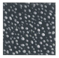
도 1은 실시예 1에서 얻어진 금속계 입자 집합체 박막을 바로 위에서 보았을 때의 SEM 화상(10000배 및 50000배 스케일)이다.
도 2는 실시예 1에서 얻어진 금속계 입자 집합체 박막의 AFM 화상이다.
도 3은 비교예 1에서 얻어진 은박막의 AFM 화상이다.
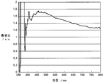
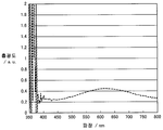
도 4는 실시예 1에서 얻어진 금속계 입자 집합체 박막 및 비교예 1에서 얻어진 은박막의 흡광 스펙트럼이다.
도 5는 참조 금속계 입자 집합체의 제조 방법을 나타내는 개략 흐름도이다.
도 6은 참조 금속계 입자 집합체 박막 적층 기판에 있어서의 참조 금속계 입자 집합체 박막을 바로 위에서 보았을 때의 SEM 화상(20000배 및 50000배 스케일)이다.
도 7은 현미경의 대물 렌즈(100배)를 이용한 흡광 스펙트럼 측정 방법을 설명하는 도면이다.
도 8은 현미경의 대물 렌즈(100배)를 이용한 방법에 따라 측정된 실시예 1에서 얻어진 금속계 입자 집합체 박막 적층 기판의 흡광 스펙트럼이다.
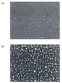
도 9는 비교예 4-1에서 얻어진 금속계 입자 집합체 박막 적층 기판에 있어서의 금속계 입자 집합체 박막을 바로 위에서 보았을 때의 SEM 화상(10000배 스케일)이다.
도 10은 비교예 4-1에서 얻어진 금속계 입자 집합체 박막 적층 기판에 있어서의 금속계 입자 집합체 박막의 AFM 화상이다.
도 11은 실시예 4-1 및 비교예 4-1에서 얻어진 금속계 입자 집합체 박막 적층 기판의, 적분구 분광 광도계를 이용한 측정법에 따른 흡광 스펙트럼이다.
도 12는 비교예 4-1에서 얻어진 금속계 입자 집합체 박막 적층 기판의, 현미경의 대물 렌즈(100배)를 이용한 측정법에 따른 흡광 스펙트럼이다.
도 13은 비교예 10-1에서 얻어진 금속계 입자 집합체 박막 적층 기판에 있어서의 금속계 입자 집합체 박막을 바로 위에서 보았을 때의 SEM 화상(10000배 및 50000배 스케일)이다.
도 14는 비교예 10-1에서 얻어진 금속계 입자 집합체 박막 적층 기판에 있어서의 금속계 입자 집합체 박막의 AFM 화상이다.
도 15는 비교예 10-1에서 얻어진 금속계 입자 집합체 박막 적층 기판의 흡광 스펙트럼이다.
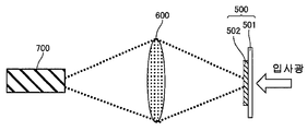
도 16의 (a)는 광 여기 발광 소자의 발광 스펙트럼의 측정 시스템을 나타내는 모식도이고, 도 16의 (b)는 금속계 입자 집합체막 및 절연층을 갖는 광 여기 발광 소자를 나타내는 단면 모식도이다.
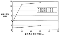
도 17은 실시예 4-1∼4-6의 광 여기 발광 소자에 있어서의 발광 증강 효과와, 비교예 4-1∼4-6의 광 여기 발광 소자에 있어서의 발광 증강 효과를 비교하는 도면이다.
도 18은 실시예 5-1∼5-5의 광 여기 발광 소자에 있어서의 발광 증강 효과와, 비교예 6-1∼6-5 및 비교예 10-1∼10-5의 광 여기 발광 소자에 있어서의 발광 증강 효과를 비교하는 도면이다.
도 19는 실시예 6-1∼6-3의 광 여기 발광 소자에 있어서의 발광 증강 효과와, 비교예 8-1∼8-3의 광 여기 발광 소자에 있어서의 발광 증강 효과를 비교하는 도면이다.1 is an SEM image (10000 times and 50000 times scale) when viewed from directly above the thin film of the metal-based grain aggregate obtained in Example 1. Fig.
Fig. 2 is an AFM image of the metal-based particle aggregate thin film obtained in Example 1. Fig.
3 is an AFM image of the silver film obtained in Comparative Example 1. Fig.
4 is an absorption spectrum of the metal-based particle aggregate thin film obtained in Example 1 and the silver thin film obtained in Comparative Example 1. Fig.
Fig. 5 is a schematic flow chart showing a method for producing a reference metal-based grain aggregate.
6 is an SEM image (20000 times and 50000 times scale) when the reference metal particle aggregate thin film in the reference metal particle aggregate thin film laminate substrate is viewed from above.
7 is a view for explaining a light absorption spectrum measuring method using an objective lens (100 times) of a microscope.
8 is an absorption spectrum of the metal-based particle-aggregate thin film laminated substrate obtained in Example 1, which was measured according to a method using an objective lens (100 times) of a microscope.
9 is an SEM image (10,000 times scale) when the metal-based particle aggregate thin film on the metal-based particle assembly thin film laminated substrate obtained in Comparative Example 4-1 is viewed from directly above.
10 is an AFM image of the metal-based particle aggregate thin film in the metal-based particle-aggregate thin film laminated substrate obtained in Comparative Example 4-1.
11 is an absorption spectrum of the thin film laminate substrate of the metal-based grain aggregated body obtained in Example 4-1 and Comparative Example 4-1 according to the measurement method using an integral spherical spectrophotometer.
12 is an absorption spectrum according to a measurement method using an objective lens (100 times) of a microscope of the thin film laminate of the metal-based grain-particle assembly obtained in Comparative Example 4-1.
13 is an SEM image (10000 times and 50000 times scale) when the metal-based particle aggregate thin film on the metal-based particle assembly thin film laminated substrate obtained in Comparative Example 10-1 is viewed from directly above.
14 is an AFM image of a metal-based particle aggregate thin film on the metal-based particle-aggregate thin film laminated substrate obtained in Comparative Example 10-1.
15 is an absorption spectrum of the metal-based grain-particle assembly thin-film laminated substrate obtained in Comparative Example 10-1.
FIG. 16A is a schematic view showing a measurement system of the light emission spectrum of a photoexcitation light emitting element, and FIG. 16B is a schematic cross-sectional view showing a photoexcitation light emitting element having a metal particle aggregate film and an insulating layer.
17 is a view for comparing the light emission enhancement effect of the photoexcitation light emitting device of Examples 4-1 to 4-6 and the light emission enhancement effect of the photoexcitation light emission device of Comparative Examples 4-1 to 4-6 .
FIG. 18 shows the light emission enhancing effect of the photoexcitation light emitting devices of Examples 5-1 to 5-5 and the light emission enhancing effect of the photoexcitation light emitting devices of Comparative Examples 6-1 to 6-5 and Comparative Examples 10-1 to 10-5 And the light emission enhancing effect in the light emitting layer.
19 is a view for comparing the light emission enhancement effect of the photoexcitation light emitting device of Examples 6-1 to 6-3 with the light emission enhancement effect of the photoexcitation light emission device of Comparative Examples 8-1 to 8-3 .
<금속계 입자 집합체의 제조 방법>≪ Process for producing metal-based grain aggregate &
본 발명의 금속계 입자 집합체의 제조 방법은, 소정 온도로 조정된 기판 상에, 매우 저속으로 금속계 입자를 성장시키는 공정(이하, 입자 성장 공정이라고도 함)을 포함하는 것이다. 이러한 입자 성장 공정을 포함하는 제조 방법에 따르면, 30개 이상의 금속계 입자가 서로 이격하여 2차원적으로 배치되어 있고, 상기 금속계 입자가, 소정 범위 내의 형상(평균 입자 직경 200 ㎚∼1600 ㎚, 평균 높이 55 ㎚∼500 ㎚ 및 애스펙트비 1∼8), 더욱 바람직하게는 소정 범위 내의 평균 입자 사이 거리(1 ㎚∼150 ㎚)를 갖는 금속계 입자 집합체의 박막을 제어성 좋게 얻을 수 있다.The method for producing the metal-based grain aggregate of the present invention includes a step of growing metal-based particles at a very low speed (hereinafter also referred to as a grain growing step) on a substrate adjusted to a predetermined temperature. According to the manufacturing method including such a grain growing step, 30 or more metal-based particles are two-dimensionally spaced apart from each other, and the metal-based particles have a shape within a predetermined range (
입자 성장 공정에 있어서, 기판 상에 금속계 입자를 성장시키는 속도는, 평균 높이 성장 속도로 1 ㎚/분 미만, 바람직하게는 0.5 ㎚/분 이하로 된다. 여기서 말하는 평균 높이 성장 속도란, 평균 퇴적 속도 또는 금속계 입자의 평균 두께 성장 속도라고도 부를 수 있고, 하기 식:In the grain growth process, the rate of growth of the metal-based particles on the substrate is less than 1 nm / min, preferably 0.5 nm / min or less, at the average height growth rate. The average height growth rate referred to herein may also be referred to as an average deposition rate or an average thickness growth rate of metal-based particles,
금속계 입자의 평균 높이/금속계 입자 성장 시간(금속계 재료의 공급 시간)Average height of metal-based particles / metal-based particle growth time (supply time of metal-based materials)
으로 정의된다. 「금속계 입자의 평균 높이」의 정의는 후술하는 바와 같다.. The definition of " average height of metal-based particles "
입자 성장 공정에 있어서의 기판의 온도는, 100℃∼450℃의 범위 내로 되고, 바람직하게는 200℃∼450℃, 보다 바람직하게는 250℃∼350℃, 더욱 바람직하게는 300℃ 또는 그 근방(300℃±10℃ 정도)이다.The temperature of the substrate in the grain growth process is in the range of 100 to 450 占 폚, preferably 200 to 450 占 폚, more preferably 250 to 350 占 폚, and more preferably 300 占 폚 or near 300 DEG C +/- 10 DEG C).
100℃∼450℃의 범위 내로 온도 조정된 기판 상에, 1 ㎚/분 미만의 평균 높이 성장 속도로 금속계 입자를 성장시키는 입자 성장 공정을 포함하는 본 발명의 제조 방법에서는, 입자 성장 초기에 있어서, 공급된 금속계 재료로 이루어지는 섬형상 구조물이 복수 형성되고, 이 섬형상 구조물이, 추가적인 금속계 재료의 공급을 받아 크게 성장하면서, 주위의 섬형상 구조물과 합체해 가며, 그 결과, 개개의 금속계 입자가 서로 완전하게 분리되어 있으면서도, 비교적 평균 입자 직경이 큰 입자가 조밀하게 배치된 금속계 입자 집합체가 형성된다. 따라서, 소정 범위 내의 형상(평균 입자 직경, 평균 높이 및 애스펙트비), 더욱 바람직하게는 소정 범위 내의 평균 입자 사이 거리를 갖도록 제어된 금속계 입자로 이루어지는 금속계 입자 집합체를 제조하는 것이 가능해진다.In the manufacturing method of the present invention, which includes a grain growth step of growing metal-based grains at an average height growth rate of less than 1 nm / min on a substrate whose temperature has been adjusted within a range of 100 ° C to 450 ° C, A plurality of island-like structures made of the supplied metal-based materials are formed, and the island-like structures are supplied with additional metal-based materials and coalesced with surrounding island-shaped structures while greatly growing. As a result, A metal-based grain aggregate in which particles having a relatively large mean particle diameter are densely arranged is formed while being completely separated. Therefore, it becomes possible to produce a metal-based grain aggregate composed of metal-based particles controlled to have a shape within a predetermined range (average particle diameter, average height and aspect ratio), more preferably a distance between average particles within a predetermined range.
또한, 평균 높이 성장 속도, 기판 온도 및/또는 금속계 입자의 성장 시간(금속계 재료의 공급 시간)의 조정에 의해, 기판 상에 성장되는 금속계 입자의 평균 입자 직경, 평균 높이, 애스펙트비 및/또는 평균 입자 사이 거리를 소정의 범위 내에서 제어하는 것도 가능하다.Further, by adjusting the average height growth rate, the substrate temperature and / or the growth time of the metal-based particles (the supply time of the metal-based material), the average particle diameter, the average height, the aspect ratio, and / or the average It is also possible to control the distance between particles within a predetermined range.
또한, 본 발명의 제조 방법에 따르면, 입자 성장 공정에 있어서의 기판 온도 및 평균 높이 성장 속도 이외의 여러가지 조건을 비교적 자유롭게 선택할 수 있기 때문에, 원하는 사이즈의 기판 상에 원하는 사이즈의 금속계 입자 집합체 박막을 효율적으로 형성할 수 있다고 하는 이점도 있다.Further, according to the manufacturing method of the present invention, various conditions other than the substrate temperature and the average height growth rate in the grain growth step can be selected relatively freely, so that the metal-based grain aggregate thin film of a desired size can be efficiently As shown in Fig.
평균 높이 성장 속도가 1 ㎚/분 이상인 경우나, 기판 온도가 100℃ 미만 또는 450℃를 넘는 경우에는, 섬형상 구조물이 크게 성장하기 전에 주위의 섬형상 구조물과 연속체를 형성하여, 서로 완전하게 분리된 대입자 직경의 금속계 입자로 이루어지는 금속계 집합체를 얻을 수 없거나, 또는, 원하는 형상을 갖는 금속계 입자로 이루어지는 금속계 집합체를 얻을 수 없다(예컨대 평균 높이나 평균 입자 사이 거리, 애스펙트비가 원하는 범위로부터 벗어나 버림).When the average height growth rate is 1 nm / min or more, or when the substrate temperature is lower than 100 deg. C or higher than 450 deg. C, a continuum is formed with the surrounding island structure before the island structure grows large, It is impossible to obtain a metal-based aggregate composed of metal-based particles having a large particle diameter or a metal-based aggregate composed of metal-based particles having a desired shape (for example, the average height and the distance between the average particles and the aspect ratio deviate from the desired range).
금속계 입자를 성장시킬 때의 압력(장치 챔버 내의 압력)은, 입자 성장 가능한 압력인 한 특별히 제한되지 않지만, 통상, 대기압 미만이다. 압력의 하한은 특별히 제한되지 않지만, 평균 높이 성장 속도를 상기 범위 내로 조정하기 쉽기 때문에, 바람직하게는 6 ㎩ 이상, 보다 바람직하게는 10 ㎩ 이상, 더욱 바람직하게는 30 ㎩ 이상이다.The pressure at which the metal-based particles are grown (the pressure in the apparatus chamber) is not particularly limited as long as it is a pressure capable of grain growth, but is usually lower than atmospheric pressure. The lower limit of the pressure is not particularly limited, but is preferably 6 Pa or more, more preferably 10 Pa or more, and further preferably 30 Pa or more because it is easy to adjust the average height growth rate within the above range.
기판 상에 금속계 입자를 성장시키는 구체적 방법은, 1 ㎚/분 미만의 평균 높이 성장 속도로 입자 성장시킬 수 있는 방법인 한 특별히 제한되지 않지만, 스퍼터링법, 진공 증착 등의 증착법을 들 수 있다. 스퍼터링법 중에서도, 비교적 간편하게 금속계 입자 집합체를 성장시킬 수 있고, 또한, 1 ㎚/분 미만의 평균 높이 성장 속도를 유지하기 쉽기 때문에, 직류(DC) 스퍼터링법을 이용하는 것이 바람직하다. 스퍼터링 방식은 특별히 제한되지 않고, 이온 건이나 플라즈마 방전으로 발생한 아르곤 이온을 전계로 가속하여 타겟에 조사하는 직류 아르곤 이온 스퍼터링법 등을 이용할 수 있다. 스퍼터링법에 있어서의 전류값, 전압값, 기판·타겟 사이 거리 등의 다른 여러가지 조건은, 1 ㎚/분 미만의 평균 높이 성장 속도로 입자 성장이 이루어지도록 적절하게 조정된다.A specific method of growing the metal-based particles on the substrate is not particularly limited as long as the method can grow the particles at an average height growth rate of less than 1 nm / minute, and examples thereof include a vapor deposition method such as a sputtering method and a vacuum deposition method. Among the sputtering methods, it is preferable to use the direct current (DC) sputtering method because the metal-based grain aggregate can be relatively easily grown and the average height growth rate of less than 1 nm / minute can be easily maintained. The sputtering method is not particularly limited, and a direct current argon ion sputtering method in which argon ions generated by an ion gun or a plasma discharge are accelerated by an electric field to irradiate a target can be used. Various other conditions such as a current value, a voltage value, and a distance between the substrate and the target in the sputtering method are appropriately adjusted so that the grain growth is carried out at an average height growth rate of less than 1 nm / min.
또한, 소정 범위 내의 형상(평균 입자 직경, 평균 높이 및 애스펙트비), 더욱 바람직하게는 소정 범위 내의 평균 입자 사이 거리를 갖는 금속계 입자로 이루어지는 금속계 입자 집합체의 박막을 제어성 좋게 얻기 위해서는, 입자 성장 공정에 있어서 평균 높이 성장 속도를 1 ㎚/분 미만으로 하는 것에 더하여, 평균 입자 직경 성장 속도를 5 ㎚ 미만으로 하는 것이 바람직하지만, 평균 높이 성장 속도가 1 ㎚/분 미만인 경우, 통상, 평균 입자 직경 성장 속도는 5 ㎚ 미만이 된다. 평균 입자 직경 성장 속도는, 보다 바람직하게는 1 ㎚/분 이하이다. 평균 입자 직경 성장 속도란, 하기 식:In order to controllably obtain a thin film of a metal-based grain aggregate composed of metal-based particles having a shape within a predetermined range (average particle diameter, average height and aspect ratio), more preferably a distance between average particles within a predetermined range, It is preferable to set the average height growth rate to less than 1 nm / min. In addition, when the average height growth rate is less than 1 nm / min, The speed is less than 5 nm. The average particle diameter growth rate is more preferably 1 nm / min or less. The average particle diameter growth rate refers to the following formula:
금속계 입자의 평균 입자 직경/금속계 입자 성장 시간(금속계 재료의 공급 시간)Average particle diameter of metal-based particles / metal-based particle growth time (supply time of metal-based material)
으로 정의된다. 「금속계 입자의 평균 입자 직경」의 정의는 후술하는 바와 같다.. The definition of " average particle diameter of metal-based particles "
입자 성장 공정에 있어서의 금속계 입자의 성장 시간(금속계 재료의 공급 시간)은, 적어도, 기판 상에 담지된 금속계 입자가 소정 범위 내의 형상, 더욱 바람직하게는 소정 범위 내의 평균 입자 사이 거리에 달하는 시간이고, 또한, 상기 소정 범위 내의 형상, 평균 입자 사이 거리로부터 일탈하기 시작하는 시간 미만이다. 예컨대, 상기 소정 범위 내의 평균 높이 성장 속도 및 기판 온도로 입자 성장을 행하여도, 성장 시간이 극단적으로 지나치게 긴 경우에는, 금속계 재료의 담지량이 지나치게 많아져, 서로 이격하여 배치된 금속계 입자의 집합체는 되지 않고 연속막이 되거나, 금속계 입자의 평균 입자 직경이나 평균 높이가 지나치게 커지거나 한다.The growth time (supply time of the metal-based material) of the metal-based particles in the grain growth process is at least the time for the metal-based particles carried on the substrate to reach a shape within a predetermined range, more preferably a distance between average particles within a predetermined range , And also the shape within the predetermined range, less than the time which starts to deviate from the distance between the average particles. For example, even if the grain growth is carried out at the average height growth rate and the substrate temperature within the predetermined range, if the growth time is extremely excessively long, the amount of the metal-based material to be supported is excessively large and aggregates of the metal- Or the average particle diameter or average height of the metal-based particles becomes excessively large.
따라서, 금속계 입자의 성장 시간을 적절한 시간으로 설정할(입자 성장 공정을 적절한 시간에 정지할) 필요가 있지만, 이러한 시간의 설정은, 예컨대, 미리 예비 실험을 행함으로써 얻어지는, 평균 높이 성장 속도 및 기판 온도와, 얻어지는 금속계 입자 집합체에 있어서의 금속계 입자의 형상 및 평균 입자 사이 거리의 관계에 기초하여 행할 수 있다. 혹은, 기판 상에 성장된 금속계 재료로 이루어지는 박막이 도전성을 나타내기까지의 시간(즉, 박막이 금속계 입자 집합체막이 아니라, 연속막이 되어 버리는 시간)을 미리 예비 실험에 의해 구해 두고, 이 시간에 달할 때까지 입자 성장 공정을 정지하도록 하여도 좋다.Therefore, it is necessary to set the growth time of the metal-based particles to an appropriate time (to stop the particle growth step at an appropriate time), but such setting of the time can be made, for example, And the relationship between the shape of the metal-based particles and the distance between the average particles in the obtained metal-based particle aggregate. Alternatively, a preliminary experiment may be carried out in advance to obtain the time until the thin film made of the metal-based material grown on the substrate exhibits conductivity (that is, the time when the thin film becomes a continuous film instead of the metal-based particle aggregate film) The particle growth process may be stopped.
금속계 입자 집합체를 구성하는 금속계 입자(기판 상에 공급되는 금속계 재료)는, 나노 입자 또는 그 집합체로 하였을 때에, 흡광 광도법에 따른 흡광 스펙트럼 측정에 있어서 자외∼가시 영역에 나타나는 플라즈몬 공명 피크(이하, 플라즈몬 피크라고도 함)를 나타내는 재료로 이루어지는 한 특별히 한정되지 않고, 예컨대, 금, 은, 동, 백금, 팔라듐 등의 귀금속이나, 알루미늄, 탄탈 등의 금속; 상기 귀금속 또는 금속을 함유하는 합금; 상기 귀금속 또는 금속을 포함하는 금속 화합물(금속 산화물이나 금속염 등)을 들 수 있다. 이들 중에서도, 금, 은, 동, 백금, 팔라듐 등의 귀금속이 바람직하고, 저렴하며 흡수가 작다(가시광 파장에 있어서 유전 함수의 허수 부분이 작다)고 하는 관점에서는 은인 것이 보다 바람직하다. 단, 금속계 재료의 종류는, 금속계 입자 집합체를 증강 요소로서 적용하는 광학 소자의 종류에 따라 적절하게 선택되는 것이 바람직하다.When the metal particles constituting the metal-based particle aggregate (metal-based material supplied onto the substrate) are nanoparticles or aggregates thereof, the plasmon resonance peaks appearing in the ultraviolet to visible region in the absorption spectrum measurement according to the absorption spectrophotometry (Also referred to as a peak), and examples thereof include noble metals such as gold, silver, copper, platinum and palladium, metals such as aluminum and tantalum; An alloy containing the noble metal or metal; And metal compounds (such as metal oxides and metal salts) containing the noble metal or metal. Of these, noble metals such as gold, silver, copper, platinum and palladium are preferable, and silver is more preferable from the viewpoints of low cost and low absorption (the imaginary part of the dielectric function is small at visible light wavelength). It is preferable that the kind of the metal-based material is appropriately selected depending on the kind of the optical element to which the metal-based grain aggregate is applied as the enhancing element.
여기서, 본 발명의 제조 방법에 따라 얻어지는 기판 상에 형성되는 금속계 입자 집합체의 박막에 있어서, 금속계 입자 간은 서로 절연되어 있는, 바꾸어 말하면, 인접하는 금속계 입자와의 사이에 관해서 비도전성(금속계 입자 집합체 박막으로서 비도전성)인 것이 바람직하다. 일부 혹은 모든 금속계 입자 사이에서 전자의 전달이 가능하기 때문에, 플라즈몬 피크는 첨예함을 잃고, 벌크 금속의 흡광 스펙트럼에 근접하며, 또한 높은 플라즈몬 공명이 얻어지지 않는다. 따라서, 금속계 입자 간은 확실하게 이격되어 있고, 금속계 입자 간에는 도전성 물질이 개재되지 않는 것이 바람직하다.Here, in the thin film of the metal-based particle aggregate formed on the substrate obtained according to the production method of the present invention, the metal-based particles are electrically insulated from each other, that is, between adjacent metal- Non-conductive as a thin film). Since electrons can be transmitted between some or all of the metal-based particles, the plasmon peak loses sharpness, is close to the absorption spectrum of the bulk metal, and high plasmon resonance is not obtained. Therefore, it is preferable that the metal-based particles are reliably spaced apart from each other, and that no conductive material intervenes between the metal-based particles.
금속계 입자 집합체 박막의 비도전성을 확보하는 관점에서, 기판으로서는 비도전성 기판을 이용하는 것이 바람직하다. 비도전성 기판으로서는, 유리, 각종 무기 절연 재료(SiO2, ZrO2, 운모 등), 각종 플라스틱 재료를 이용할 수 있다. 그 중에서도, 예컨대 발광 소자에 적용하였을 때에, 기판 표면(금속계 입자 집합체 박막과는 반대측의 면)으로부터의 광 취출이 가능하게 되기 때문에, 투광성을 갖는 기판을 이용하는 것이 바람직하고, 광학적으로 투명한 기판을 이용하는 것이 보다 바람직하다.From the viewpoint of ensuring the non-conductivity of the metal-based particle aggregate thin film, it is preferable to use a non-conductive substrate as the substrate. As the non-conductive substrate, glass, various inorganic insulating materials (SiO 2 , ZrO 2 , mica, etc.), and various plastic materials can be used. In particular, when applied to, for example, a light emitting device, light can be taken out from the surface of the substrate (the surface opposite to the surface of the metal-based particle aggregate thin film), so it is preferable to use a substrate having translucency, Is more preferable.
금속계 입자를 성장시키는 기판 표면은, 될 수 있는 한 평활한 것이 바람직하고, 특히, 예컨대 운모의 박리면과 같이 원자 레벨로 평활한 것이 보다 바람직하다. 기판 표면이 평활할수록, 기판으로부터 수취한 열 에너지에 의해, 성장 중인 금속계 입자가 별도의 주위의 인접 금속계 입자와 합체 성장하기 쉬워지기 때문에, 보다 큰 사이즈의 금속계 입자로 이루어지는 막이 얻어지기 쉬운 경향이 있다.The surface of the substrate on which the metal-based particles are grown is preferably as smooth as possible, and more preferably smooth at an atomic level such as, for example, the surface of mica. As the surface of the substrate becomes smoother, the growing metal particles tend to coalesce with other surrounding adjacent metal particles due to thermal energy received from the substrate, so that a film made of metal particles of a larger size tends to be easily obtained .
또한, 본 발명의 제조 방법은, 뒤에 상세하게 서술하는 바와 같이, 금속계 입자 집합체의 박막 표면에 절연층을 형성하는 공정을 포함하고 있어도 좋다.Further, the manufacturing method of the present invention may include a step of forming an insulating layer on the thin film surface of the metal-based grain aggregate, as described in detail later.
<금속계 입자 집합체>≪ Metal-based particle aggregate &
전술한 바와 같이, 본 발명에 따른 제조 방법에 따르면, 30개 이상의 금속계 입자가 서로 이격하여 2차원적으로 배치되어 있고, 상기 금속계 입자의 평균 입자 직경이 200 ㎚∼1600 ㎚의 범위 내, 평균 높이가 55 ㎚∼500 ㎚의 범위 내, 평균 높이에 대한 평균 입자 직경의 비로 정의되는 애스펙트비가 1∼8의 범위 내인 금속계 입자 집합체의 박막을 제어성 좋게 얻을 수 있다.As described above, according to the production method of the present invention, 30 or more metal-based particles are two-dimensionally arranged apart from each other, and the average particle diameter of the metal-based particles is within a range of 200 nm to 1600 nm, Having an aspect ratio within a range of 1 to 8, which is defined as a ratio of an average particle diameter to an average height within a range of 55 nm to 500 nm, can be obtained with good controllability.
본 발명에 따른 제조 방법에 따라 얻어지는 금속계 입자 집합체는, 더욱 하기의 어느 하나의 특징을 갖는다.The metal-based grain aggregate obtained by the production method according to the present invention further has any of the following characteristics.
〔i〕금속계 입자 집합체를 구성하는 금속계 입자가, 그 인접하는 금속계 입자와의 평균 거리(평균 입자 사이 거리)가 1 ㎚∼150 ㎚의 범위 내가 되도록 배치되어 있다,[I] The metal-based particles constituting the metal-based particle aggregate are arranged such that the average distance (distance between the average particles) to the adjacent metal-based particles is in the range of 1 nm to 150 nm.
〔ii〕금속계 입자 집합체는, 가시광 영역에 있어서의 흡광 스펙트럼에 있어서, 상기 평균 입자 직경과 동일한 입자 직경, 상기 평균 높이와 동일한 높이 및 동일한 재질로 이루어지는 금속계 입자를, 금속계 입자 사이의 거리가 전부 1 ㎛∼2 ㎛의 범위 내가 되도록 배치한 참조 금속계 입자 집합체(X)와 비교하여, 가장 장파장측에 있는 피크의 극대 파장이 30 ㎚∼500 ㎚의 범위에서 단파장측으로 시프트하고 있다,[Ii] The metal-based grain aggregate preferably has a particle diameter equal to the average particle diameter, a height equal to the average height, and the same material as the metal-based particle in the absorption spectrum in the visible light region, The maximum wavelength of the peak on the longest wavelength side is shifted to the short wavelength side in the range of 30 nm to 500 nm as compared with the reference metal-based particle aggregate (X)
〔iii〕금속계 입자 집합체는, 가시광 영역에 있어서의 흡광 스펙트럼에 있어서, 상기 평균 입자 직경과 동일한 입자 직경, 상기 평균 높이와 동일한 높이 및 동일한 재질로 이루어지는 금속계 입자를, 금속계 입자 사이의 거리가 전부 1 ㎛∼2 ㎛의 범위 내가 되도록 배치한 참조 금속계 입자 집합체(Y)보다, 동일한 금속계 입자수에서의 비교에 있어서, 가장 장파장측에 있는 피크의 극대 파장에 있어서의 흡광도가 높다.[Iii] The metal-based grain aggregate preferably has a particle diameter equal to the average particle diameter, a height equal to the average height, and the same material as the metal-based particles in the light absorption spectrum in the visible light region, The absorbance at the maximum wavelength of the peak on the longest wavelength side is higher than that of the reference metal-based particle aggregate (Y) arranged so as to fall within the range of from 2 to 2 mu m.
본 명세서에 있어서, 금속계 입자 집합체의 평균 입자 직경 및 평균 높이가 참조 금속계 입자 집합체(X) 또는 (Y)와 「동일」하다는 것은, 평균 입자 직경의 차가 ±5 ㎚의 범위 내이며, 평균 높이의 차가 ±10 ㎚의 범위 내인 것을 말한다.In the present specification, the mean particle diameter and average height of the metal-based particle aggregate are " the same as the reference metal-based particle aggregate (X) or (Y) " And the difference is within ± 10 nm.
(금속계 입자 집합체〔i〕)(Metal-based grain aggregate [i])
상기 〔i〕의 특징을 갖는 금속계 입자 집합체(금속계 입자 집합체〔i〕)는, 다음 점에 있어서 매우 유리하다.The metal-based grain aggregate (metal-based grain aggregate [i]) having the feature [i] described above is very advantageous in the following respects.
(1) 극히 강한 플라즈몬 공명을 나타내기 때문에, 발광 소자에 적용한 경우에는, 종래의 플라즈몬 재료를 이용하는 경우와 비교하여, 보다 강한 발광 증강 효과를 얻을 수 있고, 이에 의해 발광 효율을 비약적으로 높일 수 있다. 또한, 광전 변환 소자에 적용한 경우에는, 그 변환 효율을 비약적으로 높일 수 있다. 금속계 입자 집합체〔i〕가 나타내는 플라즈몬 공명의 강도는, 특정 파장에 있어서의 개개의 금속계 입자가 나타내는 국재 플라즈몬 공명의 단순한 총합이 아니며, 그 이상의 강도이다. 즉, 30개 이상의 소정 형상의 금속계 입자가 상기 소정 간격으로 조밀하게 배치됨으로써, 개개의 금속계 입자가 상호 작용하여, 극히 강한 플라즈몬 공명이 발현된다. 이것은, 금속계 입자의 국재 플라즈몬 사이의 상호 작용에 의해 발현된 것으로 생각된다.(1) Since it exhibits extremely strong plasmon resonance, when applied to a light emitting device, a stronger luminescence enhancing effect can be obtained as compared with the case of using a conventional plasmon material, and thereby the luminescence efficiency can be drastically increased . Further, when applied to a photoelectric conversion element, the conversion efficiency can be dramatically increased. The strength of the plasmon resonance represented by the metal-based grain aggregate [i] is not a simple sum of local plasmon resonance represented by the individual metal-based particles at a specific wavelength, but is more than that. That is, since 30 or more metal particles having a predetermined shape are densely arranged at the predetermined intervals, the individual metal particles interact with each other, and an extremely strong plasmon resonance is expressed. It is considered that this is expressed by the interaction between the local plasmons of the metal-based particles.
일반적으로 플라즈몬 재료는, 흡광 광도법으로 흡광 스펙트럼을 측정하였을 때, 자외∼가시 영역에 있어서의 피크로서 플라즈몬 피크가 관측되고, 이 플라즈몬 피크의 극대 파장에 있어서의 흡광도값의 대소로부터, 그 플라즈몬 재료의 플라즈몬 공명의 강도를 약식으로 평가할 수 있지만, 유리 기판 상에 형성된 금속계 입자 집합체〔i〕는, 흡광 스펙트럼을 측정하였을 때, 가시광 영역에 있어서 가장 장파장측에 있는 플라즈몬 피크의 극대 파장에 있어서의 흡광도가 1 이상, 또한 1.5 이상, 더욱 2 정도가 될 수 있다.Generally, a plasmon material exhibits a plasmon peak as a peak in the ultraviolet to visible region when the absorption spectrum is measured by the absorption spectrophotometry. From the magnitude of the absorbance at the maximum wavelength of the plasmon peak, The intensity of the plasmon resonance can be evaluated in an abbreviated manner. However, when the absorption spectrum of the metal-based particle aggregate [i] formed on the glass substrate is measured, the absorbance at the maximum wavelength of the plasmon peak on the longest wavelength side in the
금속계 입자 집합체의 흡광 스펙트럼은, 유리 기판 상에 형성한 것을 측정 샘플로 하여, 흡광 광도법에 따라 측정된다. 구체적으로는, 흡광 스펙트럼은, 금속계 입자 집합체 박막이 적층된 유리 기판의 이면측(금속계 입자 집합체 박막과는 반대측)으로서, 기판면에 수직인 방향으로부터 자외∼가시광 영역의 입사광을 조사하고, 금속계 입자 집합체 박막측에 투과한 전체 방향에 있어서의 투과광의 강도(I)와, 상기 측정 샘플의 기판과 동일한 두께, 재질의 기판으로서, 금속계 입자 집합체 박막이 적층되어 있지 않은 기판의 면에 수직인 방향으로부터 이전과 동일한 입사광을 조사하며, 입사면의 반대측으로부터 투과한 전체 방향에 있어서의 투과광의 강도(I0)를, 각각 적분구 분광 광도계를 이용하여 측정함으로써 얻어진다. 이때, 흡광 스펙트럼의 종축인 흡광도는, 하기 식:The absorption spectrum of the metal-based grain aggregate is measured by a spectrophotometric method using a sample formed on a glass substrate as a measurement sample. Concretely, the absorption spectrum is obtained by irradiating incident light in the ultraviolet to visible light region from the direction perpendicular to the substrate surface, on the back side (opposite to the metal-based particle aggregate thin film) of the glass substrate on which the metal- The intensity (I) of the transmitted light in the entire direction transmitted to the aggregate thin film side and the intensity (I) of the transmitted light from the direction perpendicular to the plane of the substrate on which the metal- Is obtained by irradiating the same incident light as before and measuring the intensity (I 0 ) of the transmitted light in the entire direction transmitted from the opposite side of the incident surface by using an integral spherical spectrophotometer. At this time, the absorbance, which is the ordinate of the absorption spectrum,
흡광도=-log10(I/I0)Absorbance = -log 10 (I / I 0 )
으로 나타낸다.Respectively.
(2) 플라즈몬 공명의 작용 범위(플라즈몬에 의한 증강 효과가 미치는 범위)가 현저하게 신장되어 있다. 이러한 신장 작용도 또한, 30개 이상의 소정 형상의 금속계 입자를 소정 간격으로 조밀하게 배치함으로써 생긴 금속계 입자의 국재 플라즈몬 사이의 상호 작용에 의해 발현된 것으로 생각된다. 금속계 입자 집합체〔i〕에 의하면, 종래에는 대략 푀르스터 거리의 범위 내(약 10 ㎚ 이하)로 한정되어 있던 플라즈몬 공명의 작용 범위를, 예컨대 수백 ㎚ 정도까지 신장시킬 수 있다.(2) the range of action of plasmon resonance (the range of enhancement effect by plasmon) is remarkably elongated. It is also believed that this elongation is also manifested by the interaction between the internally-generated plasmons of the metal-based particles formed by densely arranging the metal-based particles of 30 or more predetermined shapes at predetermined intervals. According to the metal-based grain aggregate [i], the action range of plasmon resonance, which has been conventionally limited within the range of the approximate Louverst distance (about 10 nm or less), can be extended to, for example, several hundreds nm.
상기와 같은 플라즈몬 공명의 작용 범위의 신장은, 발광 소자나 광전 변환 소자(태양 전자 소자 등) 등의 광학 소자의 증강에 매우 유리하다. 즉, 이 작용 범위의 대폭적인 신장에 의해, 통상 수십 ㎚ 또는 그 이상의 두께를 갖는 활성층(발광 소자에 있어서의 발광층이나 광전 변환 소자에 있어서의 광흡수층 등)의 전체를 증강시키는 것이 가능해지고, 이에 의해 광학 소자의 증강 효과(발광 효율이나 변환 효율 등)를 현저하게 향상시킬 수 있다.The elongation of the action range of plasmon resonance as described above is very advantageous for the enhancement of optical elements such as light emitting elements and photoelectric conversion elements (solar electronic elements, etc.). In other words, it is possible to increase the entirety of the active layer (light-emitting layer in the light-emitting element or light-absorbing layer in the photoelectric conversion element) having a thickness of usually several tens nm or more, The luminous efficiency (luminous efficiency, conversion efficiency, etc.) of the optical element can be remarkably improved.
또한, 종래의 플라즈몬 재료에 있어서는, 플라즈몬 재료를 활성층과의 거리가 푀르스터 거리의 범위 내가 되도록 배치할 필요가 있었지만, 금속계 입자 집합체〔i〕에 의하면, 활성층으로부터, 예컨대 10 ㎚, 또한 수십 ㎚(예컨대 20 ㎚), 더욱 수백 ㎚ 떨어진 위치에 배치하여도 플라즈몬 공명에 의한 증강 효과를 얻을 수 있다. 이것은, 예컨대 발광 소자라면, 발광층으로부터 상당히 떨어진 광 취출면 근방에 플라즈몬 재료(금속계 입자 집합체)를 배치하는 것이 가능하게 되는 것을 의미하고 있으며, 이에 의해 광 취출 효율을 대폭으로 향상시킬 수 있다. 종래의 플라즈몬 재료를 이용한 발광 소자에서는, 플라즈몬 재료를 발광층의 매우 근방에 배치하지 않을 수 없어, 플라즈몬 재료와 광 취출면의 거리가 크게 떨어져 있었기 때문에, 발생한 광이 광 취출면에 도달하기까지의 동안에, 그 대부분이, 통과하는 각종 발광 소자 구성층의 계면에서 전반사되어 버려, 광 취출 효율이 매우 작아지는 일이 있었다.In the conventional plasmon material, it is necessary to arrange the plasmon material so that the distance from the active layer is within the range of the Stokes distance. According to the metal-based particle aggregate [i], however, For example, 20 nm), and even if it is disposed at a position away from a few hundred nanometers, an enhancing effect by plasmon resonance can be obtained. This means that, for example, in the case of a light-emitting element, it becomes possible to dispose a plasmon material (metal-based particle aggregate) in the vicinity of the light-extracting surface, which is considerably distant from the light-emitting layer. In the light emitting device using the conventional plasmon material, it is necessary to arrange the plasmon material in the very vicinity of the light emitting layer, and since the distance between the plasmon material and the light emitting surface is large, , Most of the light is totally reflected at the interface between the various light emitting device constituent layers passing therethrough, and the light extraction efficiency may be very small.
이와 같이 금속계 입자 집합체〔i〕는, 그 단독으로는 쌍극자형의 국재 플라즈몬이 가시광 영역에서 생기하기 어려운 비교적 대형의 금속계 입자를 이용함에도 불구하고, 이러한 대형의 금속계 입자(소정의 형상을 갖고 있는 것이 필요하지만)의 특정수 이상을, 특정한 간격을 두고 조밀하게 배치함으로써, 상기 대형의 금속계 입자가 내포하는 극히 다수의 표면 자유 전자를 유효하게 플라즈몬으로서 여기할 수 있어, 현저하게 강한 플라즈몬 공명 및 플라즈몬 공명의 작용 범위의 현저한 신장의 실현을 가능하게 한 것이다.Although the metal-based particle aggregate [i] alone uses relatively large metal-based particles in which the dipole-type localized plasmons are hardly generated in the visible light region, such large metal-based particles (having a predetermined shape It is possible to effectively excite a large number of surface free electrons contained in the large metal-based particles effectively as a plasmon, and to achieve remarkably strong plasmon resonance and plasmon resonance Thereby realizing a remarkable elongation of the working range of the present invention.
또한, 금속계 입자 집합체〔i〕는, 특정한 형상을 갖는 비교적 대형인 금속계 입자의 특정수 이상을 2차원적으로 특정한 간격으로 이격하여 배치한 구조를 갖고 있는 것에 기인하여, 다음과 같은 유리한 효과를 나타낼 수 있다.Further, the metal-based grain aggregate [i] has the following advantageous effects owing to the structure in which a specified number or more of relatively large metal-based particles having a specific shape are two-dimensionally spaced apart at specific intervals .
(3) 가시광 영역에 있어서의 흡광 스펙트럼에 있어서, 금속계 입자의 평균 입자 직경 및 평균 입자 사이 거리에 의존하여, 플라즈몬 피크의 극대 파장이 특이한 시프트를 나타낼 수 있다. 구체적으로는, 평균 입자 사이 거리를 일정하게 하여 금속계 입자의 평균 입자 직경을 크게 함에 따라, 가시광 영역에 있어서 가장 장파장측에 있는 플라즈몬 피크의 극대 파장이 단파장측으로 시프트(블루 시프트)한다. 마찬가지로, 대형의 금속계 입자의 평균 입자 직경을 일정하게 하여 평균 입자 사이 거리를 작게 함에 따라(금속계 입자를 보다 조밀하게 배치하면), 가시광 영역에 있어서 가장 장파장측에 있는 플라즈몬 피크의 극대 파장이 단파장측으로 시프트한다. 이 특이한 현상은, 플라즈몬 재료에 관해서 일반적으로 인정되고 있는 미 산란 이론〔이 이론에 따르면, 입자 직경이 커지면 플라즈몬 피크의 극대 파장은 장파장측으로 시프트(레드 시프트)한다.〕에 반하는 것이다.(3) In the absorption spectrum in the visible light region, the maximum wavelength of the plasmon peak may exhibit a peculiar shift, depending on the average particle diameter of the metal-based particles and the distance between the average particles. Concretely, the maximum wavelength of the plasmon peak on the longest wavelength side in the visible light region shifts (blue shifts) to the short wavelength side as the average particle diameter of the metal-based particles is increased by keeping the distance between the average particles constant. Likewise, when the average particle diameter of the large metal-based particles is made constant and the distance between the average particles is made small (when the metal-based particles are densely arranged), the maximum wavelength of the plasmon peak on the longest wavelength side in the visible light region becomes shorter Shift. This peculiar phenomenon is contrary to the generally accepted scattering theory for plasmon materials (according to this theory, the maximum wavelength of the plasmon peak shifts to the longer wavelength side (red shift) when the particle diameter becomes large).
상기와 같은 특이한 블루 시프트도 또한, 금속계 입자 집합체〔i〕가 대형의 금속계 입자를 특정한 간격을 두고 조밀하게 배치한 구조를 가지고 있고, 이에 따라, 금속계 입자의 국재 플라즈몬 사이의 상호 작용이 생기고 있는 것에 의한 것으로 생각된다. 금속계 입자 집합체〔i〕(유리 기판 상에 적층한 상태)는, 금속계 입자의 형상이나 평균 입자 사이 거리에 따라, 흡광 광도법에 따라 측정되는 가시광 영역에 있어서의 흡광 스펙트럼에 있어서, 가장 장파장측에 있는 플라즈몬 피크가, 예컨대 350 ㎚∼550 ㎚의 파장 영역에 극대 파장을 나타낼 수 있다. 또한, 금속계 입자 집합체〔i〕는, 금속계 입자가 충분히 긴 입자 사이 거리(예컨대 1 ㎛)를 두고 배치되는 경우와 비교하여, 전형적으로는 30 ㎚∼500 ㎚ 정도(예컨대 30 ㎚∼250 ㎚)의 블루 시프트를 발생시킬 수 있다.The above-mentioned peculiar blue shift also has a structure in which the metal-based grain aggregate [i] has a structure in which large metal-based grains are densely arranged at specific intervals, and thus the interaction between the internally- . The metal-based grain aggregate [i] (in a state of being laminated on a glass substrate) has a maximum absorption spectrum in the absorption spectrum in the visible light region measured according to the absorption spectrophotometry, depending on the shape of the metal- The plasmon peak can exhibit a maximum wavelength in a wavelength range of 350 nm to 550 nm, for example. In addition, the metal-based grain aggregate [i] has a grain size of about 30 nm to about 500 nm (for example, about 30 nm to about 250 nm), which is typically about 30 nm to about 500 nm in comparison with the case where the metal- Blue shift can be generated.
이러한, 종래의 것과 비교하여 플라즈몬 피크의 극대 파장이 블루 시프트하고 있는 금속계 입자 집합체는, 예컨대 다음 점에서 매우 유리하다. 즉, 높은 발광 효율을 나타내는 청색(혹은 그 근방 파장 영역, 이하 동일) 발광 재료(특히 청색 인광 재료)의 실현이 강하게 요구되고 있는 한편, 충분히 실용에 견디는 이러한 재료의 개발이 현재 상황에서는 곤란한 바, 예컨대 청색의 파장 영역에 플라즈몬 피크를 갖는 금속계 입자 집합체〔i〕를 증강 요소로서 발광 소자에 적용함으로써, 비교적 발광 효율이 낮은 청색 발광 재료를 이용하는 경우라도, 그 발광 효율을 충분한 정도로까지 증강시킬 수 있다. 또한, 광전 변환 소자(태양 전지 소자 등)에 적용한 경우에는, 예컨대 공명 파장을 블루 시프트시킴으로써 활성층 자체에서는 이용할 수 없었던 파장 영역을 유효 이용할 수 있게 되어, 변환 효율을 향상시킬 수 있다.Such a metal-based grain aggregate in which the maximum wavelength of the plasmon peak is blue-shifted as compared with the conventional one is very advantageous, for example, in the following points. In other words, it is strongly desired to realize a blue light emitting material (particularly a blue light emitting material) that exhibits a high light emitting efficiency. However, it is difficult in the present situation to develop such a material that can withstand practical use sufficiently, For example, by applying the metal particle aggregate [i] having a plasmon peak in a blue wavelength region to a light emitting element as an enhancing element, even when a blue light emitting material having a relatively low light emitting efficiency is used, the light emitting efficiency can be increased to a sufficient level . In addition, when applied to a photoelectric conversion element (solar cell element or the like), for example, by blue-shifting the resonance wavelength, it is possible to effectively use the wavelength region that was not available in the active layer itself, and the conversion efficiency can be improved.
다음에, 금속계 입자 집합체〔i〕의 구체적 구성에 대해서 보다 상세하게 설명한다.Next, the specific constitution of the metal-based grain aggregate [i] will be described in more detail.
금속계 입자의 평균 입자 직경은 200 ㎚∼1600 ㎚의 범위 내이며, 상기 (1)∼(3)의 효과를 효과적으로 얻기 위해, 바람직하게는 200 ㎚∼1200 ㎚, 보다 바람직하게는 250 ㎚∼500 ㎚, 더욱 바람직하게는 300 ㎚∼500 ㎚의 범위 내이다. 금속계 입자의 평균 입자 직경은, 금속계 입자 집합체를 증강 요소로서 적용하는 광학 소자의 종류나 금속계 입자를 구성하는 재료의 종류에 따라 적절하게 선택되는 것이 바람직하다.The average particle diameter of the metal-based particles is in the range of 200 nm to 1600 nm and is preferably 200 nm to 1200 nm, more preferably 250 nm to 500 nm, in order to effectively obtain the effects (1) to (3) , More preferably in the range of 300 nm to 500 nm. The average particle diameter of the metal-based particles is desirably appropriately selected depending on the kind of the optical element to which the metal-based particle aggregate is applied as the enhancing element and the kind of the material constituting the metal-based particle.
여기서 특필하여야 할 점은, 예컨대 평균 입자 직경 500 ㎚라고 하는 대형의 금속계 입자는, 전술한 바와 같이, 그 단독으로는 국재 플라즈몬에 의한 증강 효과가 거의 인정되지 않는다고 하는 것이다. 이에 대하여 금속계 입자 집합체〔i〕는, 이러한 대형의 금속계 입자의 소정수(30개) 이상을 소정의 간격으로 조밀하게 배치함으로써, 현저하게 강한 플라즈몬 공명 및 플라즈몬 공명의 작용 범위의 현저한 신장, 더욱 상기 (3)의 효과를 실현하는 것이다.It should be noted here that, as described above, large metal particles having an average particle diameter of 500 nm, for example, are rarely recognized by the local plasmon as an enhancing effect. On the other hand, the metal-based grain aggregate [i] has a remarkably strong plasmon resonance and remarkable elongation of the action range of plasmon resonance, (3).
금속계 입자의 평균 입자 직경이란, 2차원적으로 금속계 입자가 배치된 금속계 입자 집합체 박막의 바로 위로부터의 SEM 관찰 화상에 있어서, 무작위로 입자를 10개 선택하고, 각 입자상 내에 무작위로 접선 직경을 5개 그어(단, 접선 직경이 되는 직선은 모두 입자상 내부만을 통과할 수 있으며, 이 중 1개는 입자 내부만을 통과하여, 가장 길게 그어지는 직선인 것으로 함), 그 평균값을 각 입자의 입자 직경으로 하였을 때의, 선택한 10개의 입자 직경의 평균값이다. 접선 직경이란, 입자의 윤곽(투영상)을 이것에 접하는 2개의 평행선으로 사이에 끼웠을 때의 간격(닛칸코교신분샤 「입자 계측 기술」, 1994, 제5 페이지)을 연결하는 수선으로 정의한다.The average particle diameter of the metal-based particles means that 10 particles are randomly selected in an SEM observation image just above a thin film of the metal-based particle aggregate on which the metal-based particles are two-dimensionally arranged, randomly tangent diameters within each particle are set to 5 (The straight line having a tangential diameter can pass only through the interior of the particle, one of which passes through only the inside of the particle and is regarded as a straight line drawn the longest), and the average value is set to the particle diameter of each particle , The average value of the diameters of the ten selected particles. The tangential diameter is defined as a line connecting the contour (projection) of the particle with the interval between two parallel lines touching it (Nikken Kogyo Shinbunsha "Particle Measurement Technology", 1994, page 5) .
금속계 입자의 평균 높이는 55 ㎚∼500 ㎚의 범위 내이며, 상기 (1)∼(3)의 효과를 효과적으로 얻기 위해, 바람직하게는 55 ㎚∼300 ㎚, 보다 바람직하게는 70 ㎚∼150 ㎚의 범위 내이다. 금속계 입자의 평균 높이란, 금속계 입자 집합체 박막의 AFM 관찰 화상에 있어서, 무작위로 입자를 10개 선택하고, 이들 10개의 입자의 높이를 측정하였을 때의, 10개의 측정값의 평균값이다.The average height of the metal-based particles is in the range of 55 nm to 500 nm and is preferably in the range of 55 nm to 300 nm, more preferably in the range of 70 nm to 150 nm, in order to effectively obtain the effects (1) to (3) It is mine. The average height of the metal-based particles is an average value of 10 measured values when 10 particles are randomly selected and the height of these 10 particles is measured in the AFM observation image of the thin film of the metal-based particle aggregate.
금속계 입자의 애스펙트비는 1∼8의 범위 내이며, 범위 내에서 금속계 입자 집합체를 증강 요소로서 적용하는 광학 소자의 종류에 따라 적절하게 선택하는 것이 바람직하다. 예컨대 발광 소자의 증강 요소로서 이용하는 경우에는, 금속계 입자는 편평 형상을 갖는 것이 바람직한 경향이 있고, 이 경우, 보다 높은 증강 효과를 얻기 위해, 애스펙트비는 2∼8인 것이 바람직하며, 2.5∼8인 것이 보다 바람직하다. 한편, 광전 변환 소자의 증강 요소로서 이용하는 경우, 보다 높은 증강 효과를 얻기 위해서는, 금속계 입자는 완전 구형에 가까울수록 바람직한 경향이 있다. 금속계 입자의 애스펙트비는, 상기 평균 높이에 대한 상기 평균 입자 직경의 비(평균 입자 직경/평균 높이)로 정의된다.The aspect ratio of the metal-based particles is in the range of 1 to 8, and it is preferable that the aspect ratio is appropriately selected depending on the kind of the optical element to which the metal-based particle aggregate is applied as the enhancing element. For example, when used as an enhancing element of a light-emitting element, it is preferable that the metal-based particles have a flat shape. In this case, in order to obtain a higher enhancing effect, the aspect ratio is preferably 2 to 8, Is more preferable. On the other hand, when used as an enhancing element of a photoelectric conversion element, in order to obtain a higher enhancing effect, metal-based particles tend to be closer to a perfectly spherical shape. The aspect ratio of the metal-based particles is defined as a ratio (average particle diameter / average height) of the average particle diameter to the average height.
금속계 입자는, 효과가 높은 플라즈몬을 여기하는 관점에서, 그 표면이 매끄러운 곡면으로 이루어지는 것이 바람직하지만, 표면에 미소한 요철(거칠기)을 어느 정도 포함하고 있어도 좋고, 이러한 의미에 있어서 금속계 입자는 부정형이어도 좋다.Although it is preferable that the metal-based particles have a smooth curved surface from the viewpoint of exciting the highly effective plasmons, the metal-based particles may contain minute unevenness (roughness) on the surface. In this sense, the metal- good.
금속계 입자 집합체의 면내에 있어서의 플라즈몬 공명의 강도의 균일성을 감안하여, 금속계 입자 사이의 사이즈의 불균일은 될 수 있는 한 작은 것이 바람직하다. 단, 입자 직경에 다소 불균일이 생겼다고 해도, 대형 입자 사이의 거리가 커지는 것은 바람직하지 못하고, 그 사이를 소형의 입자가 매립함으로써 대형 입자 사이의 상호 작용을 발현하기 쉽게 하는 것이 바람직하다.In consideration of the uniformity of the intensity of the plasmon resonance in the plane of the metal-based grain aggregate, it is preferable that the size irregularity among the metal-based grains is as small as possible. However, even if the particle diameter is somewhat uneven, it is not preferable that the distance between the large particles is large, and it is preferable that the small particles are embedded between the large particles to facilitate the interaction between the large particles.
금속계 입자 집합체〔i〕에 있어서 금속계 입자는, 그 인접하는 금속계 입자와의 평균 거리(평균 입자 사이 거리)가 1 ㎚∼150 ㎚의 범위 내가 되도록 배치된다. 이와 같이 금속계 입자를 조밀하게 배치함으로써, 현저하게 강한 플라즈몬 공명 및 플라즈몬 공명의 작용 범위의 현저한 신장, 더욱 상기 (3)의 효과를 실현시킬 수 있다. 평균 입자 사이 거리는, 상기 (1)∼(3)의 효과를 효과적으로 얻기 위해, 바람직하게는 1 ㎚∼100 ㎚, 보다 바람직하게는 1 ㎚∼50 ㎚, 더욱 바람직하게는 1 ㎚∼20 ㎚의 범위 내이다. 평균 입자 사이 거리가 1 ㎚ 미만이면, 입자 간에서 덱스터 기구에 기초한 전자 이동이 생겨, 국재 플라즈몬의 실활의 점에서 불리해진다.In the metal-based grain aggregate [i], the metal-based particles are arranged such that the average distance (distance between the average particles) to the adjacent metal-based particles is in the range of 1 nm to 150 nm. By densely arranging the metal-based particles in this way, remarkably strong plasmon resonance and remarkable elongation of the action range of plasmon resonance can be achieved, and the effect (3) can be further realized. The average particle distance is preferably in the range of 1 nm to 100 nm, more preferably in the range of 1 nm to 50 nm, and still more preferably in the range of 1 nm to 20 nm, in order to effectively obtain the effects (1) to (3) It is mine. If the distance between the average particles is less than 1 nm, electron movement based on the Dexter mechanism occurs between the particles, which is disadvantageous in view of inactivation of the local plasmon.
평균 입자 사이 거리란, 2차원적으로 금속계 입자가 배치된 금속계 입자 집합체 박막의 바로 위로부터의 SEM 관찰 화상에 있어서, 무작위로 입자를 30개 선택하고, 선택한 각각의 입자에 대해서, 인접하는 입자와의 입자 사이 거리를 구하였을 때의, 이들 30개의 입자의 입자 사이 거리의 평균값이다. 인접하는 입자와의 입자 사이 거리란, 모든 인접하는 입자와의 거리(표면끼리 사이의 거리임)를 각각 측정하여, 이들을 평균한 값이다.The average particle-to-particle distance is a distance between particles of the metal-based particle-assembled body in which the metal-based particles are arranged two-dimensionally. Is the mean value of the distance between the particles of these 30 particles. The distance between particles with adjacent particles is a value obtained by measuring the distance between all the adjacent particles (the distance between the surfaces), and averaging them.
금속계 입자 집합체〔i〕에 포함되는 금속계 입자의 수는 30개 이상이며, 바람직하게는 50개 이상이다. 금속계 입자를 30개 이상 포함하는 집합체를 형성함으로써, 금속계 입자의 국재 플라즈몬 사이의 상호 작용에 의해 극히 강한 플라즈몬 공명 및 플라즈몬 공명의 작용 범위의 신장이 발현된다.The number of the metal-based particles contained in the metal-based grain aggregate [i] is 30 or more, and preferably 50 or more. By forming an aggregate containing 30 or more metal-based particles, extremely strong plasmon resonance and elongation of the action range of plasmon resonance are expressed by interaction between the internally-generated plasmons of the metal-based particles.
금속계 입자 집합체〔i〕를 증강 소자로서 광학 소자에 적용하는 경우, 광학 소자의 일반적인 소자 면적에 비추어 보면, 금속계 입자 집합체〔i〕에 포함되는 금속계 입자의 수는, 예컨대 300개 이상, 더욱 17500개 이상이 될 수 있다.When the metal-based grain aggregate [i] is applied to an optical element as an enhancement element, the number of metal-based grains contained in the metal-based grain aggregate [i] is 300 or more, Or more.
금속계 입자 집합체〔i〕에 있어서의 금속계 입자의 수밀도(number density)는, 7개/㎛2 이상인 것이 바람직하고, 15개/㎛2 이상인 것이 보다 바람직하다.The number density of the metal-based particles in the metal-based grain aggregate [i] is preferably 7 / μm 2 or more, more preferably 15 / μm 2 or more.
(금속계 입자 집합체〔ii〕)(Metal particle aggregate [ii])
상기 〔ii〕의 특징을 갖는 금속계 입자 집합체(금속계 입자 집합체〔ii〕)는, 다음 점에 있어서 매우 유리하다.The metal-based particle aggregate (metal-based particle aggregate [ii]) having the characteristics of the above-mentioned [ii] is very advantageous in the following respects.
(I) 가시광 영역에 있어서의 흡광 스펙트럼에 있어서, 가장 장파장측에 있는 플라즈몬 피크의 극대 파장이 특이적인 파장 영역에 존재한다. 구체적으로는, 금속계 입자 집합체〔ii〕는, 흡광 스펙트럼을 측정하였을 때, 상기 플라즈몬 피크의 극대 파장이, 후술하는 참조 금속계 입자 집합체(X)의 극대 파장에 비해서, 30 ㎚∼500 ㎚의 범위(예컨대 30 ㎚∼250 ㎚의 범위)에서 단파장측으로 시프트(블루 시프트)하고 있고, 전형적으로는, 상기 플라즈몬 피크의 극대 파장은 350 ㎚∼550 ㎚의 범위 내에 있다.(I) In the absorption spectrum in the visible light region, the maximum wavelength of the plasmon peak on the longest wavelength side exists in a specific wavelength region. Concretely, the metal-based particle aggregate [ii] has a maximum wavelength of the plasmon peak in a range of 30 nm to 500 nm (as compared with the maximum wavelength of the reference metal-based particle aggregate (X) (Blue shift) toward the shorter wavelength side in the range of, e.g., 30 nm to 250 nm. Typically, the maximum wavelength of the plasmon peak is in the range of 350 nm to 550 nm.
이러한 청색 또는 그 근방 파장 영역에 플라즈몬 피크를 가질 수 있는 금속계 입자 집합체〔ii〕는, 청색 또는 그 근방 파장 영역의 발광 재료를 이용한 발광 소자의 발광 증강 등에 매우 유용하며, 이러한 금속계 입자 집합체〔ii〕를 구비하는 발광 소자에서는, 비교적 발광 효율이 낮은 청색 발광 재료를 이용하는 경우라도, 그 발광 효율을 충분한 정도로까지 증강시킬 수 있다. 또한, 광전 변환 소자(태양 전지 소자 등)에 적용한 경우에는, 예컨대 공명 파장을 블루 시프트시킴으로써 활성층 자체에서는 이용할 수 없었던 파장 영역을 유효 이용할 수 있게 되어, 변환 효율을 향상시킬 수 있다.The metal-based grain aggregate [ii] capable of having a plasmon peak in the blue or near-wavelength region is very useful for light emission enhancement of a light-emitting element using a light emitting material of blue or near wavelength region, It is possible to increase the luminous efficiency to a sufficient level even when a blue light emitting material having a relatively low luminous efficiency is used. In addition, when applied to a photoelectric conversion element (solar cell element or the like), for example, by blue-shifting the resonance wavelength, it is possible to effectively use the wavelength region that was not available in the active layer itself, and the conversion efficiency can be improved.
상기 블루 시프트는, 금속계 입자 집합체〔ii〕가 특정한 형상을 갖는 대형의 금속계 입자의 특정수 이상을 2차원적으로 이격하여 배치한 구조를 가지고 있고, 이에 따라, 금속계 입자의 국재 플라즈몬 사이의 상호 작용이 생기고 있는 것에 의한 것으로 생각된다.The blue shift has a structure in which the metal-based particle aggregate [ii] has a specific number or more of a large number of metal-based particles having a specific shape arranged two-dimensionally apart from each other. Thus, the interaction between metal- Is thought to be due to what is happening.
여기서, 어떤 금속계 입자 집합체와 참조 금속계 입자 집합체(X) 사이에서 가장 장파장측에 있는 피크의 극대 파장이나 그 극대 파장에 있어서의 흡광도를 비교하는 경우에는, 양자에 대해서, 현미경(Nikon사 제조 「OPTIPHOT-88」)과 분광 광도계(오오츠카덴시사 제조 「MCPD-3000」)를 이용하여, 측정 시야를 좁혀 흡광 스펙트럼 측정을 행한다.Here, when comparing the maximum wavelength of the peak on the longest wavelength side between the certain metal-based grain aggregate and the reference metal-based grain aggregate (X) or the absorbance at the maximum wavelength thereof, a microscope ("OPTIPHOT -88 ") and a spectrophotometer (" MCPD-3000 "manufactured by OTSUKA DENKI Co., Ltd.) are used to measure the absorption spectrum by narrowing the measurement visual field.
참조 금속계 입자 집합체(X)는, 흡광 스펙트럼 측정의 대상이 되는 금속계 입자 집합체가 갖는 평균 입자 직경, 평균 높이와 동일한 입자 직경, 높이 및 동일한 재질을 갖는 금속계 입자(A)를, 금속계 입자 사이의 거리가 전부 1 ㎛∼2 ㎛의 범위 내가 되도록 배치한 금속계 입자 집합체로서, 유리 기판에 적층한 상태로, 상기 현미경을 이용한 흡광 스펙트럼 측정을 행할 수 있는 정도의 크기를 갖는 것이다.The reference metal particle aggregate (X) is obtained by dispersing the metal particle (A) having the average particle diameter, the average particle diameter, the height and the same material of the metal particle aggregate as the object of the absorption spectrum measurement, Is in the range of 1 占 퐉 to 2 占 퐉 and has such a size as to be capable of performing absorption spectroscopy using the microscope in a state of being laminated on a glass substrate.
참조 금속계 입자 집합체(X)의 흡광 스펙트럼 파형은, 금속계 입자(A)의 입자 직경 및 높이, 금속계 입자(A)의 재질의 유전 함수, 금속계 입자(A) 주변의 매체(예컨대 공기)의 유전 함수, 기판(예컨대 유리 기판)의 유전 함수를 이용하여, 3D-FDTD법에 따라 이론상 계산하는 것도 가능하다.The absorption spectral waveform of the reference metal particle aggregate (X) is determined by the particle diameter and height of the metal-based particle (A), the dielectric function of the material of the metal-based particle (A) , It is also possible to calculate theoretically according to the 3D-FDTD method using the dielectric function of the substrate (e.g., glass substrate).
또한, 금속계 입자 집합체〔ii〕는, 특정한 형상을 갖는 비교적 대형인 금속계 입자의 특정수 이상을 2차원적으로 이격하여 배치한 구조를 갖고 있는 것에 기인하여, (II) 극히 강한 플라즈몬 공명을 나타낼 수 있고(상기 금속계 입자 집합체〔i〕의 효과 (1)과 동일), 및 (III) 플라즈몬 공명의 작용 범위(플라즈몬에 의한 증강 효과가 미치는 범위)가 현저하게 신장될 수 있는(상기 금속계 입자 집합체〔i〕의 효과 (2)와 동일), 등의 효과를 나타낼 수 있다. 금속계 입자 집합체〔ii〕는, 이것을 유리 기판 상에 적층한 상태로 흡광 스펙트럼을 측정하였을 때, 가시광 영역에 있어서 가장 장파장측에 있는 플라즈몬 피크의 극대 파장에 있어서의 흡광도가 1 이상, 또한 1.5 이상, 더욱 2 정도가 될 수 있다.Further, the metal-based grain aggregate [ii] has a structure in which a specific number or more of relatively large metal-based particles having a specific shape are arranged two-dimensionally apart from each other, and (II) exhibits extremely strong plasmon resonance (The same as the effect (1) of the metal-based grain aggregate [i]) and (III) the range of action of the plasmon resonance (the range of enhancement by plasmons) i] (the same as the effect (2)), and the like. The metal-based particle aggregate [ii] has an absorbance at a maximum wavelength of the plasmon peak on the longest wavelength side in the visible light region of not less than 1, more preferably not less than 1.5, It can be about two more.
금속계 입자 집합체〔ii〕의 구체적 구성은, 금속계 입자 집합체〔i〕의 구체적 구성(금속계 입자의 재질, 평균 입자 직경, 평균 높이, 애스펙트비, 평균 입자 사이 거리, 금속계 입자의 수, 금속계 입자 집합체의 비도전성 등)과 기본적으로는 동일하게 할 수 있다. 평균 입자 직경, 평균 높이, 애스펙트비, 평균 입자 사이 거리 등의 용어의 정의도 금속계 입자 집합체〔i〕와 동일하다.The specific constitution of the metal-based particle aggregate [ii] is preferably a specific constitution of the metal-based grain aggregate [i] (the material of the metal-based particle, the average particle diameter, the average height, the aspect ratio, the distance between the average particles, Non-conductivity, etc.) can be made basically the same. The definitions of the mean particle diameter, the average height, the aspect ratio, the distance between the average particles, and the like are also the same as those of the metal particle aggregate [i].
금속계 입자의 평균 입자 직경은 200 ㎚∼1600 ㎚의 범위 내이며, 상기 (I)∼(III)의 효과를 효과적으로 얻기 위해, 바람직하게는 200 ㎚∼1200 ㎚, 보다 바람직하게는 250 ㎚∼500 ㎚, 더욱 바람직하게는 300 ㎚∼500 ㎚의 범위 내이다. 이러한 대형의 금속계 입자의 소정수(30개) 이상을 2차원적으로 배치한 집합체로 함으로써, 현저하게 강한 플라즈몬 공명 및 플라즈몬 공명의 작용 범위가 현저한 신장의 실현이 가능해진다. 또한, 상기 〔ii〕의 특징(단파장측으로의 플라즈몬 피크의 시프트)을 발현시키는 데 있어서도, 금속계 입자는, 평균 입자 직경이 200 ㎚ 이상인 것이 필수이며, 바람직하게는 250 ㎚ 이상이다. 금속계 입자의 평균 입자 직경은, 금속계 입자 집합체를 증강 요소로서 적용하는 광학 소자의 종류나 금속계 입자를 구성하는 재료의 종류에 따라 적절하게 선택되는 것이 바람직하다.The average particle diameter of the metal-based particles is in the range of 200 nm to 1600 nm, preferably 200 nm to 1200 nm, more preferably 250 nm to 500 nm, in order to effectively obtain the effects (I) to (III) , More preferably in the range of 300 nm to 500 nm. By forming the aggregate in which two or more predetermined number (30 or more) of such large metal-based particles are arranged, it is possible to realize a remarkably strong elongation with a remarkable range of action of plasmon resonance and plasmon resonance. Also, in expressing the characteristic (shift of the plasmon peak to the short wavelength side) of the above-mentioned [ii], the metal-based particles are required to have an average particle diameter of 200 nm or more, and preferably 250 nm or more. The average particle diameter of the metal-based particles is desirably appropriately selected depending on the kind of the optical element to which the metal-based particle aggregate is applied as the enhancing element and the kind of the material constituting the metal-based particle.
금속계 입자 집합체〔ii〕에서는, 가시광 영역에 있어서 가장 장파장측에 있는 플라즈몬 피크의 극대 파장은, 금속계 입자의 평균 입자 직경에 의존한다. 즉, 금속계 입자의 평균 입자 직경이 일정한 값을 넘으면, 상기 플라즈몬 피크의 극대 파장은 단파장측으로 시프트(블루 시프트)한다.In the metal-based particle aggregate [ii], the maximum wavelength of the plasmon peak on the longest wavelength side in the visible light region depends on the average particle diameter of the metal-based particles. That is, when the average particle diameter of the metal-based particles exceeds a predetermined value, the maximum wavelength of the plasmon peak shifts to the short wavelength side (blue shift).
금속계 입자의 평균 높이는 55 ㎚∼500 ㎚의 범위 내이며, 상기 (I)∼(III)의 효과를 효과적으로 얻기 위해, 바람직하게는 55 ㎚∼300 ㎚, 보다 바람직하게는 70 ㎚∼150 ㎚의 범위 내이다. 금속계 입자의 애스펙트비는 1∼8의 범위 내이며, 금속계 입자 집합체〔i〕와 마찬가지로, 범위 내에서 금속계 입자 집합체를 증강 요소로서 적용하는 광학 소자의 종류에 따라 적절하게 선택하는 것이 바람직하다.The average height of the metal-based particles is in the range of 55 nm to 500 nm and is preferably in the range of 55 nm to 300 nm, more preferably in the range of 70 nm to 150 nm in order to effectively obtain the effects (I) to (III) It is mine. The aspect ratio of the metal-based particles is in the range of 1 to 8, and it is preferable that the aspect ratio is appropriately selected according to the type of the optical element to which the metal-based particle aggregate is applied as the enhancing element within the range.
금속계 입자 집합체〔ii〕에 있어서 금속계 입자는, 평균 입자 사이 거리가 1 ㎚∼150 ㎚의 범위 내가 되도록 배치되는 것이 바람직하다. 보다 바람직하게는 1 ㎚∼100 ㎚, 더욱 바람직하게는 1 ㎚∼50 ㎚, 특히 바람직하게는 1 ㎚∼20 ㎚의 범위 내이다. 이와 같이 금속계 입자를 조밀하게 배치함으로써, 금속계 입자의 국재 플라즈몬 사이의 상호 작용이 효과적으로 생겨, 상기 (I)∼(III)의 효과가 발현되기 쉬워진다. 플라즈몬 피크의 극대 파장은, 금속계 입자의 평균 입자 사이 거리에 의존하기 때문에, 평균 입자 사이 거리의 조정에 의해, 가장 장파장측에 있는 플라즈몬 피크의 블루 시프트의 정도나 그 플라즈몬 피크의 극대 파장을 제어하는 것이 가능하다. 평균 입자 사이 거리가 1 ㎚ 미만이면, 입자 간에서 덱스터 기구에 기초한 전자 이동이 생겨, 국재 플라즈몬의 실활의 점에서 불리해진다.The metal-based particles in the metal-based particle aggregate [ii] are preferably arranged so that the distance between the average particles is in the range of 1 nm to 150 nm. More preferably 1 nm to 100 nm, further preferably 1 nm to 50 nm, particularly preferably 1 nm to 20 nm. By densely arranging the metal-based particles in this way, the interactions between the local plasmons of the metal-based particles are effectively produced, and the effects (I) to (III) described above are easily exhibited. Since the maximum wavelength of the plasmon peak depends on the distance between the average particles of the metal-based particles, by adjusting the distance between the average particles, the degree of blue shift of the plasmon peak on the longest wavelength side and the maximum wavelength of the plasmon peak are controlled It is possible. If the distance between the average particles is less than 1 nm, electron movement based on the Dexter mechanism occurs between the particles, which is disadvantageous in view of inactivation of the local plasmon.
금속계 입자 집합체〔ii〕에 포함되는 금속계 입자의 수는 30개 이상이며, 바람직하게는 50개 이상이다. 금속계 입자를 30개 이상 포함하는 집합체를 형성함으로써, 금속계 입자의 국재 플라즈몬 사이의 상호 작용이 효과적으로 생겨, 상기 〔ii〕의 특징 및 상기 (I)∼(III)의 효과의 발현이 가능해진다.The number of the metal-based particles contained in the metal-based particle aggregate [ii] is 30 or more, preferably 50 or more. By forming aggregates containing 30 or more metal-based particles, interactions between the internally-generated plasmons of the metal-based particles are effectively produced, and the characteristics of the above-mentioned [ii] and the effects of the above (I) to (III) can be manifested.
금속계 입자 집합체〔ii〕를 증강 소자로서 광학 소자에 적용하는 경우, 광학 소자의 일반적인 소자 면적에 비추어 보면, 금속계 입자 집합체〔ii〕에 포함되는 금속계 입자의 수는, 예컨대 300개 이상, 더욱 17500개 이상이 될 수 있다.When the metal-based particle aggregate [ii] is applied to an optical element as an enhancement element, the number of the metal-based particles contained in the metal-based grain aggregate [ii] is 300 or more, Or more.
금속계 입자 집합체〔ii〕에 있어서의 금속계 입자의 수밀도는, 7개/㎛2 이상인 것이 바람직하고, 15개/㎛2 이상인 것이 보다 바람직하다.The number density of the metal-based particles in the metal-based particle aggregate [ii] is not less than 7 / ㎛ 2, and more preferably larger than 15 / ㎛ 2.
(금속계 입자 집합체〔iii〕)(Metal particle aggregate [iii])
상기 〔iii〕의 특징을 갖는 금속계 입자 집합체(금속계 입자 집합체〔iii〕)는, 다음 점에 있어서 매우 유리하다.The metal-based grain aggregate (metal-based grain aggregate [iii]) having the feature [iii] described above is very advantageous in the following respects.
(A) 플라즈몬 피크인 가시광 영역에 있어서 가장 장파장측에 있는 피크의 극대 파장에 있어서의 흡광도가, 금속계 입자가 아무런 입자 사이 상호 작용도 없이 단순하게 집합한 집합체라고 간주할 수 있는 후술하는 참조 금속계 입자 집합체(Y)보다 크고, 따라서, 극히 강한 플라즈몬 공명을 나타내기 때문에, 발광 소자에 적용한 경우에는, 종래의 플라즈몬 재료를 이용하는 경우와 비교하여, 보다 강한 발광 증강 효과를 얻을 수 있으며, 이에 의해 발광 효율을 비약적으로 높일 수 있다. 또한, 광전 변환 소자에 적용한 경우에는, 이 변환 효율을 비약적으로 높일 수 있다. 이러한 강한 플라즈몬 공명은, 금속계 입자의 국재 플라즈몬 사이의 상호 작용에 의해 발현된 것으로 생각된다.(A) the absorbance at the maximum wavelength of the peak on the longest wavelength side in the visible light region which is the plasmon peak, can be regarded as an aggregate in which the metal-based particles are simply aggregated without any interaction between particles, Is larger than the aggregate (Y), and thus exhibits extremely strong plasmon resonance. Therefore, when applied to a light emitting device, a stronger luminescent enhancing effect can be obtained as compared with the case of using a conventional plasmon material, Can be dramatically increased. Further, in the case where the present invention is applied to a photoelectric conversion element, the conversion efficiency can be dramatically increased. This strong plasmon resonance is believed to be expressed by the interaction between the metal plasmons and the local plasmons.
상기한 바와 같이, 플라즈몬 피크의 극대 파장에 있어서의 흡광도값의 대소로부터, 그 플라즈몬 재료의 플라즈몬 공명의 강도를 약식으로 평가하는 것이 가능하지만, 금속계 입자 집합체〔iii〕는, 이것을 유리 기판 상에 적층한 상태로 흡광 스펙트럼을 측정하였을 때, 가시광 영역에 있어서 가장 장파장측에 있는 플라즈몬 피크의 극대 파장에 있어서의 흡광도가 1 이상, 또한 1.5 이상, 더욱 2 정도가 될 수 있다.As described above, the intensity of the plasmon resonance of the plasmon material can be evaluated sharply from the magnitude of the absorbance at the maximum wavelength of the plasmon peak, but the metal-based particle aggregate [iii] The absorbance at the maximum wavelength of the plasmon peak on the longest wavelength side in the visible light region can be 1 or more, more preferably 1.5 or more, or even 2 or so.
전술한 바와 같이, 어떤 금속계 입자 집합체와 참조 금속계 입자 집합체(Y) 사이에서 가장 장파장측에 있는 피크의 극대 파장이나 그 극대 파장에 있어서의 흡광도를 비교하는 경우에는, 양자에 대해서, 현미경(Nikon사 제조 「OPTIPHOT-88」)과 분광 광도계(오오츠카덴시사 제조 「MCPD-3000」)를 이용하여, 측정 시야를 좁혀 흡광 스펙트럼 측정을 행한다.As described above, when comparing the maximum wavelength of the peak on the longest wavelength side between the certain metal-based grain aggregate and the reference metal-based grain aggregate (Y) or the absorbance at the maximum wavelength, they are measured with a microscope Quot; OPTIPHOT-88 ") and a spectrophotometer (" MCPD-3000 " manufactured by OTSUKA DENKI CO., LTD.) Are used to narrow the measurement field and perform absorption spectrophotometry.
참조 금속계 입자 집합체(Y)는, 흡광 스펙트럼 측정의 대상이 되는 금속계 입자 집합체가 갖는 평균 입자 직경, 평균 높이와 동일한 입자 직경, 높이 및 동일한 재질을 갖는 금속계 입자(B)를, 금속계 입자 사이의 거리가 전부 1 ㎛∼2 ㎛의 범위 내가 되도록 배치한 금속계 입자 집합체로서, 유리 기판에 적층한 상태로, 상기 현미경을 이용한 흡광 스펙트럼 측정을 행할 수 있는는 정도의 크기를 갖는 것이다.The reference metal particle aggregate (Y) is obtained by mixing the metal particle (B) having the average particle diameter, the particle diameter, height, and the same material as the average particle diameter and height of the metal particle aggregate to be subjected to the absorption spectrum measurement, Is in the range of 1 탆 to 2 탆, and has a size such that the absorption spectrum measurement using the microscope can be performed in a state of being laminated on a glass substrate.
흡광 스펙트럼 측정의 대상이 되는 금속계 입자 집합체와 참조 금속계 입자 집합체(Y) 사이에서, 가장 장파장측에 있는 피크의 극대 파장에 있어서의 흡광도를 비교할 때에는, 이하에 서술하는 바와 같이, 동일한 금속계 입자수가 되도록 환산한 참조 금속계 입자 집합체(Y)의 흡광 스펙트럼을 구하고, 그 흡광 스펙트럼에 있어서의 가장 장파장측에 있는 피크의 극대 파장에 있어서의 흡광도를 비교의 대상으로 한다. 구체적으로는, 금속계 입자 집합체와 참조 금속계 입자 집합체(Y)의 흡광 스펙트럼을 각각 구하고, 각각의 흡광 스펙트럼에 있어서의 가장 장파장측에 있는 피크의 극대 파장에 있어서의 흡광도를, 각각의 피복률(금속계 입자에 의한 기판 표면의 피복률)로 나눈 값을 산출하여, 이들을 비교한다.When comparing the absorbance at the maximum wavelength of the peak on the longest wavelength side between the metal particle aggregate and the reference metal particle aggregate (Y) to be subjected to the absorption spectrum measurement, as described below, Absorbing spectrum of the reference metal grain aggregate (Y) in terms of the maximum absorption wavelength at the maximum wavelength of the peak in the absorption spectrum is to be compared. Specifically, the absorption spectra of the metal-based grain aggregate and the reference metal-based grain aggregate (Y) are respectively obtained, and the absorbance at the maximum wavelength of the peak on the longest wavelength side in each absorption spectrum is measured by the respective coating rates The coating rate of the surface of the substrate by the particles) is calculated and compared.
또한, 금속계 입자 집합체〔iii〕는, 특정한 형상을 갖는 비교적 대형인 금속계 입자의 특정수 이상을 2차원적으로 이격하여 배치한 구조를 가지고 있는 것에 기인하여, (B) 플라즈몬 공명의 작용 범위(플라즈몬에 의한 증강 효과가 미치는 범위)가 현저하게 신장될 수 있고(상기 금속계 입자 집합체〔i〕의 효과 (2)와 동일), 및 (C) 플라즈몬 피크의 극대 파장이 특이한 시프트를 나타낼 수 있는(상기 금속계 입자 집합체〔i〕의 효과 (3)과 동일), 등의 효과를 나타낼 수 있다.Further, the metal-based particle aggregate [iii] has a structure in which a specific number or more of relatively large metal-based particles having a specific shape are arranged two-dimensionally apart from each other, and (B) the action range of plasmon resonance (The same effect as the effect (2) of the metal-based grain aggregate [i]), and (C) the maximum wavelength of the plasmon peak can exhibit a peculiar shift (The same as the effect (3) of the metal-based grain aggregate [i]).
금속계 입자 집합체〔iii〕(유리 기판 상에 적층한 상태)는, 금속계 입자의 형상이나 평균 입자 사이 거리에 따라, 흡광 광도법에 따라 측정되는 가시광 영역에 있어서의 흡광 스펙트럼에 있어서, 가장 장파장측에 있는 플라즈몬 피크가, 예컨대 350 ㎚∼550 ㎚의 파장 영역에 극대 파장을 나타낼 수 있다. 또한, 금속계 입자 집합체〔iii〕는, 금속계 입자가 충분히 긴 입자 사이 거리(예컨대 1 ㎛)를 두고 배치되는 경우와 비교하여, 전형적으로는 30 ㎚∼500 ㎚ 정도(예컨대 30 ㎚∼250 ㎚)의 블루 시프트를 발생시킬 수 있다.The metal-based particle aggregate [iii] (in a state of being laminated on a glass substrate) has a maximum absorption spectrum in the absorption spectrum in the visible light region measured according to the absorption spectrophotometry, depending on the shape of the metal- The plasmon peak can exhibit a maximum wavelength in a wavelength range of 350 nm to 550 nm, for example. In addition, the metal-based grain aggregate [iii] has a grain size of about 30 nm to 500 nm (for example, about 30 nm to about 250 nm), which is typically about 30 nm to about 500 nm in comparison with the case where the metal- Blue shift can be generated.
금속계 입자 집합체〔iii〕의 구체적 구성은, 금속계 입자 집합체〔i〕의 구체적 구성(금속계 입자의 재질, 평균 입자 직경, 평균 높이, 애스펙트비, 평균 입자 사이 거리, 금속계 입자의 수, 금속계 입자 집합체의 비도전성 등)과 기본적으로는 동일하게 할 수 있다. 평균 입자 직경, 평균 높이, 애스펙트비, 평균 입자 사이 거리 등의 용어의 정의도 금속계 입자 집합체〔i〕와 동일하다.The specific constitution of the metal-based grain aggregate [iii] is not particularly limited as long as the specific constitution of the metal-based grain aggregate [i] (the material of the metal-based grain, the average particle diameter, the average height, the aspect ratio, the distance between the average particles, Non-conductivity, etc.) can be made basically the same. The definitions of the mean particle diameter, the average height, the aspect ratio, the distance between the average particles, and the like are also the same as those of the metal particle aggregate [i].
금속계 입자의 평균 입자 직경은 200 ㎚∼1600 ㎚의 범위 내이며, 상기 〔iii〕의 특징(가장 장파장측에 있는 플라즈몬 피크의 극대 파장에 있어서의 흡광도가 참조 금속계 입자 집합체(Y)의 그것보다 높다고 하는 특징), 더욱 상기 (A)∼(C)의 효과를 효과적으로 얻기 위해, 바람직하게는 200 ㎚∼1200 ㎚, 보다 바람직하게는 250 ㎚∼500 ㎚, 더욱 바람직하게는 300 ㎚∼500 ㎚의 범위 내이다. 이와 같이, 비교적 대형의 금속계 입자를 형성하는 것이 긴요하며, 대형의 금속계 입자의 소정수(30개) 이상을 2차원적으로 배치한 집합체로 함으로써, 현저하게 강한 플라즈몬 공명, 더욱 플라즈몬 공명의 작용 범위의 현저한 신장, 단파장측으로의 플라즈몬 피크의 시프트의 실현이 가능해진다. 금속계 입자의 평균 입자 직경은, 금속계 입자 집합체를 증강 요소로서 적용하는 광학 소자의 종류나 금속계 입자를 구성하는 재료의 종류에 따라 적절하게 선택되는 것이 바람직하다.The average particle diameter of the metal-based particles is in the range of 200 nm to 1600 nm, and the feature [iii] (the absorbance at the maximum wavelength of the plasmon peak on the longest wavelength side is higher than that of the reference metal- In order to effectively obtain the effects of the above (A) to (C), it is preferable to set the range of 200 nm to 1200 nm, more preferably 250 nm to 500 nm, further preferably 300 nm to 500 nm It is mine. As described above, it is critical to form relatively large metal-based particles, and by forming an aggregate in which two or more predetermined number (30 or more) of large metal-based particles are arranged, remarkably strong plasmon resonance, And the shift of the plasmon peak to the short wavelength side can be realized. The average particle diameter of the metal-based particles is desirably appropriately selected depending on the kind of the optical element to which the metal-based particle aggregate is applied as the enhancing element and the kind of the material constituting the metal-based particle.
금속계 입자의 평균 높이는 55 ㎚∼500 ㎚의 범위 내이며, 상기 〔iii〕의 특징, 더욱 상기 (A)∼(C)의 효과를 효과적으로 얻기 위해, 바람직하게는 55 ㎚∼300 ㎚, 보다 바람직하게는 70 ㎚∼150 ㎚의 범위 내이다. 금속계 입자의 애스펙트비는 1∼8의 범위 내이며, 금속계 입자 집합체〔i〕와 마찬가지로, 범위 내에서 금속계 입자 집합체를 증강 요소로서 적용하는 광학 소자의 종류에 따라 적절하게 선택하는 것이 바람직하다.The average height of the metal-based particles is in the range of 55 nm to 500 nm and is preferably 55 nm to 300 nm, more preferably 55 nm to 300 nm in order to effectively obtain the characteristics of the above [iii] and the effects of the above (A) Is in the range of 70 nm to 150 nm. The aspect ratio of the metal-based particles is in the range of 1 to 8, and it is preferable that the aspect ratio is appropriately selected according to the type of the optical element to which the metal-based particle aggregate is applied as the enhancing element within the range.
상기 〔iii〕의 특징이 효과적으로 얻어지기 때문에, 금속계 입자 집합체〔iii〕를 구성하는 금속계 입자는, 이들의 사이즈 및 형상(평균 입자 직경, 평균 높이, 애스펙트비)이 될 있는 한 균일한 것이 바람직하다. 즉, 금속계 입자의 사이즈 및 형상을 균일하게 함으로써, 플라즈몬 피크가 첨예화하고, 이에 따라, 가장 장파장측에 있는 플라즈몬 피크의 흡광도가 참조 금속계 입자 집합체(Y)의 그것보다 높아지기 쉬워진다. 금속계 입자 사이의 사이즈 및 형상의 불균일의 저감은, 금속계 입자 집합체 면내에 있어서의 플라즈몬 공명의 강도의 균일성의 관점에서도 유리하다. 단 전술한 바와 같이, 입자 직경에 다소 불균일이 생겼다고 해도, 대형 입자 사이의 거리가 커지는 것은 바람직하지 못하며, 그 사이를 소형의 입자가 매립함으로써 대형 입자 사이의 상호 작용을 발현하기 쉽게 하는 것이 바람직하다.Since the characteristics of [iii] are effectively obtained, it is preferable that the metal-based particles constituting the metal-based particle aggregate [iii] are as uniform as possible in terms of their size and shape (average particle diameter, average height and aspect ratio) . That is, by making the size and shape of the metal-based particles uniform, the plasmon peak becomes sharp, and accordingly, the absorbance of the plasmon peak on the longest wavelength side becomes higher than that of the reference metal-based particle aggregate (Y). The reduction in unevenness in the size and shape between the metal-based particles is advantageous from the viewpoint of uniformity of the intensity of plasmon resonance in the surface of the metal-based particle aggregate. However, as described above, it is not preferable that the distance between the large particles is large even if the particle diameter is somewhat uneven, and it is preferable to facilitate the interaction between the large particles by embedding small particles therebetween .
금속계 입자 집합체〔iii〕에 있어서 금속계 입자는, 평균 입자 사이 거리가 1 ㎚∼150 ㎚의 범위 내가 되도록 배치되는 것이 바람직하다. 보다 바람직하게는 1 ㎚∼100 ㎚, 더욱 바람직하게는 1 ㎚∼50 ㎚, 특히 바람직하게는 1 ㎚∼20 ㎚의 범위 내이다. 이와 같이 금속계 입자를 조밀하게 배치함으로써, 금속계 입자의 국재 플라즈몬 사이의 상호 작용이 효과적으로 생겨, 상기 〔iii〕의 특징, 더욱 상기 (A)∼(C)의 효과를 효과적으로 발현시킬 수 있다. 평균 입자 사이 거리가 1 ㎚ 미만이면, 입자 간에서 덱스터 기구에 기초한 전자 이동이 생겨, 국재 플라즈몬의 실활의 점에서 불리해진다.The metal-based particles in the metal-based particle aggregate [iii] are preferably arranged so that the distance between the average particles is in the range of 1 nm to 150 nm. More preferably 1 nm to 100 nm, further preferably 1 nm to 50 nm, particularly preferably 1 nm to 20 nm. By densely arranging the metal-based particles in this way, the interaction between the internally-generated plasmons of the metal-based particles is effectively generated, and the characteristics of the above-mentioned [iii] and further the effects of the above-mentioned (A) to (C) can be effectively exhibited. If the distance between the average particles is less than 1 nm, electron movement based on the Dexter mechanism occurs between the particles, which is disadvantageous in view of inactivation of the local plasmon.
금속계 입자 집합체〔iii〕에 포함되는 금속계 입자의 수는 30개 이상이며, 바람직하게는 50개 이상이다. 금속계 입자를 30개 이상 포함하는 집합체를 형성함으로써, 금속계 입자의 국재 플라즈몬 사이의 상호 작용이 효과적으로 생겨, 상기 〔iii〕의 특징, 더욱 상기 (A)∼(C)의 효과를 효과적으로 발현시킬 수 있다.The number of the metal-based particles contained in the metal-based particle aggregate [iii] is 30 or more, preferably 50 or more. By forming aggregates containing 30 or more metal-based particles, the interactions between the internally-generated plasmons of the metal-based particles are effectively produced, and the characteristics of the [iii] and the effects of the above (A) to (C) can be effectively exhibited .
금속계 입자 집합체〔iii〕를 증강 소자로서 광학 소자에 적용하는 경우, 광학 소자의 일반적인 소자 면적에 비추어 보면, 금속계 입자 집합체〔iii〕에 포함되는 금속계 입자의 수는, 예컨대 300개 이상, 더욱 17500개 이상이 될 수 있다.When the metal-based grain aggregate [iii] is applied to an optical element as an enhancement element, the number of metal-based grains contained in the metal-based grain aggregate [iii] is 300 or more, more preferably 17500 Or more.
금속계 입자 집합체〔iii〕에 있어서의 금속계 입자의 수밀도는, 7개/㎛2 이상인 것이 바람직하고, 15개/㎛2 이상인 것이 보다 바람직하다.The number density of the metal-based particles in the metal-based particle aggregate [iii] is not less than 7 / ㎛ 2, and more preferably larger than 15/2 ㎛.
이상과 같이, 금속계 입자 집합체〔iii〕는, 이것을 구성하는 금속계 입자의 금속종, 사이즈, 형상, 금속계 입자 사이의 평균 거리 등의 제어에 의해 얻을 수 있다.As described above, the metal-based grain aggregate [iii] can be obtained by controlling the metal species, the size, the shape, the average distance between the metal-based particles, and the like of the metal-based particles constituting the metal-based grain-based aggregate [iii].
본 발명의 제조 방법에 따라 얻어지는 금속계 입자 집합체는, 상기 〔i〕∼〔iii〕 중 적어도 어느 하나의 특징을 갖는 것이며, 보다 전형적으로는, 〔i〕∼〔iii〕 중 어느 2개 이상의 특징을 가지고, 더욱 전형적으로는, 〔i〕∼〔iii〕의 모든 특징을 갖는다.The metal-based grain aggregate obtained according to the production method of the present invention has at least any one of the above-mentioned features [i] to [iii], and more typically any two or more of the features [i] to [iii] More typically, all the features of [i] to [iii].
본 발명에 있어서는, 전술한 입자 성장 공정 후에 절연층 형성 공정을 마련하여, 금속계 입자 집합체의 박막 상에, 각 금속계 입자의 표면을 덮는 절연층을 형성하여도 좋다. 이러한 절연층은, 전술한 금속계 입자 집합체 박막의 비도전성(금속계 입자 사이의 비도전성)을 담보하는 데 있어서 바람직할 뿐만 아니라, 금속계 입자 집합체를 광학 소자에 적용하는 경우에도 바람직하다. 즉, 전기 에너지 구동의 발광 소자나 광전 변환 소자 등의 광학 소자에서는, 이것을 구성하는 각 층에 전류가 흐르지만, 금속계 입자 집합체 박막에 전류가 흘러 버리면, 플라즈몬 공명에 의한 증강 효과가 충분히 얻어지지 않을 우려가 있다. 금속계 입자 집합체 박막을 캡하는 절연층을 마련함으로써, 광학 소자에 적용한 경우에 있어서도 금속계 입자 집합체 박막과, 이것에 인접하는 광학 소자의 구성층 사이의 전기적 절연을 도모할 수 있기 때문에, 금속계 입자 집합체 박막을 구성하는 금속계 입자에 전류가 주입되는 것을 방지할 수 있다.In the present invention, an insulating layer for covering the surface of each metal-based particle may be formed on the thin film of the metal-based particle aggregate by providing an insulating layer forming step after the above-described particle growth step. Such an insulating layer is preferable not only for securing the non-conductivity (non-conductivity between metal particles) of the metal-based particle aggregate thin film, but also for applying the metal-based particle aggregate to an optical element. That is, in an optical element such as a light-emitting element driven by an electric energy or a photoelectric conversion element, a current flows in each layer constituting it, but if an electric current flows in the thin film of the metal-based particle aggregate, an enhancement effect due to plasmon resonance is not sufficiently obtained There is a concern. It is possible to provide electrical insulation between the metal particle aggregate thin film and the constituent layers of the optical element adjacent to the metal particle aggregate thin film even when applied to an optical element by providing the insulating layer capping the metal particle aggregate thin film, It is possible to prevent an electric current from being injected into the metal-based particles constituting the electrode.
절연층을 구성하는 재료로서는, 양호한 절연성을 갖는 것이면 특별히 제한되지 않고, 예컨대, 스핀 온 글라스(SOG; 예컨대 유기 실록산 재료를 함유하는 것) 외에, SiO2나 Si3N4 등을 이용할 수 있다. 절연층의 두께는, 원하는 절연성이 확보되는 한 특별히 제한은 없지만, 후술하는 바와 같이 광학 소자에 적용하였을 때의 활성층(예컨대 발광 소자의 발광층이나 광전 변환 소자의 광흡수층)과 금속계 입자 집합체 박막의 거리는 가까울수록 바람직하기 때문에, 원하는 절연성이 확보되는 범위에서 얇을수록 좋다.The material constituting the insulating layer is not particularly limited as long as it has good insulating properties. For example, SiO 2 , Si 3 N 4 and the like can be used in addition to spin-on glass (SOG) containing an organosiloxane material. The thickness of the insulating layer is not particularly limited as long as the desired insulating property can be ensured. However, as will be described later, the distance between the active layer (for example, the light absorbing layer of the light emitting element or the light absorbing layer of the photoelectric conversion element) The closer the thickness is, the better the insulating property is.
본 발명의 제조 방법에 따라 얻어지는 금속계 입자 집합체는, 발광 소자, 광전 변환 소자(태양 전지 소자 등) 등의 광학 소자를 위한 증강 요소로서 매우 유용하다. 본 발명에 따른 금속계 입자 집합체를 광학 소자에 적용함으로써, 광학 소자의 발광 효율이나 변환 효율을 현저하게 향상시킬 수 있다. 금속계 입자 집합체는, 이것을 제조할 때에 이용하는 기판과 일체화한 상태로, 각종 광학 소자에 편입시킬 수 있다.The metal-based grain aggregate obtained according to the production method of the present invention is very useful as an enhancing element for optical elements such as a light-emitting element, a photoelectric conversion element (solar cell element, etc.). By applying the metal-based grain aggregate according to the present invention to an optical element, the luminous efficiency and conversion efficiency of the optical element can be remarkably improved. The metal-based grain aggregate can be incorporated in various optical elements in a state integrated with the substrate used for the production thereof.
전술한 바와 같이, 본 발명의 제조 방법에 따라 얻어지는 금속계 입자 집합체는, 극히 강한 플라즈몬 공명을 나타내고, 더욱 플라즈몬 공명의 작용 범위(플라즈몬에 의한 증강 효과가 미치는 범위)가 현저하게 신장되어 있기 때문에, 예컨대, 10 ㎚ 이상, 또한 20 ㎚ 이상, 더욱 그 이상의 두께를 갖는 활성층(발광 소자에 있어서의 발광층이나 광전 변환 소자에 있어서의 광흡수층 등)의 전체를 증강시키는 것이 가능하다. 또한, 예컨대 10 ㎚, 또한 수십 ㎚(예컨대 20 ㎚), 더욱 수백 ㎚ 이상 떨어진) 위치에 배치된 활성층도, 매우 효과적으로 증강시킬 수 있다.As described above, since the metal-based grain aggregate obtained according to the production method of the present invention exhibits extremely strong plasmon resonance and further remarkably elongates the action range of plasmon resonance (the range of enhancement by plasmon) , The active layer (the light absorbing layer in the light emitting layer or the photoelectric conversion element in the light emitting element) having a thickness of not less than 10 nm and not less than 20 nm and having a thickness not less than that of the active layer. Further, the active layer disposed at a position of 10 nm, for example, several tens nm (for example, 20 nm), more than several hundred nm or more) can also be very effectively enhanced.
또한, 플라즈몬에 의한 증강 효과는, 그 성질상, 활성층과 금속계 입자 집합체의 거리가 커질수록 작아지는 경향이 있기 때문에, 그 거리는 작을수록 바람직하다. 활성층과 금속계 입자 집합체의 거리는, 바람직하게는 100 ㎚ 이하이며, 보다 바람직하게는 20 ㎚ 이하이고, 더욱 바람직하게는 10 ㎚ 이하이다.In addition, the enhancing effect by the plasmon tends to decrease as the distance between the active layer and the metal-based particle aggregate becomes larger, so that the smaller the distance is, the better. The distance between the active layer and the metal-based grain aggregate is preferably 100 nm or less, more preferably 20 nm or less, and further preferably 10 nm or less.
활성층이 나타내는 발광 파장(예컨대 발광 소자의 경우) 또는 흡수 파장(예컨대 광전 변환 소자의 경우)의 극대 파장은, 금속계 입자 집합체의 플라즈몬 피크의 극대 파장과 일치하거나 또는 가까운 것이 바람직하다. 이에 따라, 플라즈몬 공명에 의한 증강 효과를 보다 효과적으로 높일 수 있다. 금속계 입자 집합체의 플라즈몬 피크의 극대 파장은, 이것을 구성하는 금속계 입자의 금속종, 평균 입자 직경, 평균 높이, 애스펙트비 및/또는 평균 입자 사이 거리의 조정에 의해 제어 가능하다.It is preferable that the maximum wavelength of an emission wavelength (for example, in the case of a light emitting element) or an absorption wavelength (in the case of a photoelectric conversion element, for example) represented by the active layer matches or is close to the maximum wavelength of the plasmon peak of the metal-based grain aggregate. Thus, the enhancing effect due to the plasmon resonance can be enhanced more effectively. The maximum wavelength of the plasmon peak of the metal-based particle aggregate can be controlled by adjusting the metal species, the average particle diameter, the average height, the aspect ratio, and / or the distance between the average particles of the metal particles constituting the peak.
상기 발광층은, 예컨대, 1) 색소분자를 평면형으로 배치한 단분자막으로 이루어지는 것, 2) 매트릭스 중에 색소 분자를 도핑하여 이루어지는 것, 3) 발광성 저분자로 이루어지는 것, 4) 발광성 고분자로 이루어지는 것, 등일 수 있다.The light emitting layer may be formed, for example, of 1) a monomolecular film in which dye molecules are arranged in a planar shape, 2) a dye doped in a matrix, 3) a low molecular weight luminescent material, 4) have.
1)의 발광층은, 색소 분자 함유액을 스핀 코트한 후, 용매를 제거하는 방법에 따라 얻을 수 있다. 색소 분자의 구체예는, Exciton사에서 판매되고 있는 로다민 101, 로다민 110, 로다민 560, 로다민 6G, 로다민 B, 로다민 640, 로다민 700 등의 로다민계 색소, Exciton사에서 판매되고 있는 쿠마린(503) 등의 쿠마린계 색소 등을 포함한다.1) can be obtained by spin coating the dye-containing liquid and then removing the solvent. Specific examples of dye molecules are sold by Exciton under the names Rhodamine 101, Rhodamine 110, Rhodamine 560, Rhodamine 6G, Rhodamine B, Rhodamine 640 and
2)의 발광층은, 색소 분자 및 메트릭스 재료를 함유하는 액을 스핀 코트한 후, 용매를 제거하는 방법에 따라 얻을 수 있다. 메트릭스 재료로서는, 폴리비닐알코올, 폴리메타크릴산메틸과 같은 투명 고분자를 이용할 수 있다. 색소 분자의 구체예는 1)의 발광층과 같을 수 있다.2) can be obtained by a method of spin-coating a liquid containing dye molecules and a matrix material, and then removing the solvent. As the matrix material, a transparent polymer such as polyvinyl alcohol or polymethyl methacrylate can be used. Specific examples of the dye molecule may be the same as the light emitting layer of 1).
3)의 발광층은, 스핀 코트법, 증착법을 비롯한 드라이 또는 웨트 성막법에 따라 얻을 수 있다. 발광성 저분자의 구체예는, 트리스(8-퀴놀리노레이트)알루미늄 착체〔트리스(8-히드록시퀴놀린)알루미늄 착체; Alq3〕, 비스(벤조퀴놀리노레이트)베릴륨 착체〔BeBq〕 등을 포함한다.3) can be obtained by a dry or wet film formation method including a spin coating method and a vapor deposition method. Specific examples of the luminescent low molecule include tris (8-quinolinolato) aluminum complex [tris (8-hydroxyquinoline) aluminum complex; Alq 3 ], bis (benzoquinolinolato) beryllium complex [BeBq], and the like.
4)의 발광층은, 스핀 코트법 등, 발광성 고분자 함유액을 이용한 웨트 성막법에 따라 얻을 수 있다. 발광성 고분자의 구체예는, F8BT〔폴리(9,9-디옥틸플루오렌-alt-벤조티아디아졸)〕, 폴리(p-페닐렌비닐렌), 폴리알킬티오펜과 같은 π 공액계 고분자 등을 포함한다.4) can be obtained by a wet film-forming method using a luminescent polymer-containing liquid such as a spin coating method. Specific examples of the luminescent polymer include π conjugated polymers such as F8BT [poly (9,9-dioctylfluorene-alt-benzothiadiazole)], poly (p-phenylenevinylene) .
실시예Example
이하, 실시예를 들어 본 발명을 보다 상세하게 설명하지만, 본 발명은 이들 실시예에 한정되는 것이 아니다.Hereinafter, the present invention will be described in more detail with reference to examples, but the present invention is not limited to these examples.
〔금속계 입자 집합체의 제작〕[Production of metal particle aggregate]
<실시예 1>≪ Example 1 >
직류 마그네트론 스퍼터링 장치를 이용하여, 하기의 조건으로, 소다 유리 기판 상에, 은입자를 매우 천천히 성장시켜, 기판 표면의 전체면에 금속계 입자 집합체의 박막을 형성하여, 금속계 입자 집합체 박막 적층 기판을 얻었다.Silver particles were very slowly grown on a soda glass substrate using a DC magnetron sputtering apparatus under the following conditions to form a thin film of a metal-based grain aggregate on the entire surface of the substrate to obtain a metal-based grain-particle aggregate thin film laminated substrate .
사용 가스: 아르곤,Use gas: argon,
챔버 내 압력(스퍼터 가스압): 10 ㎩,Chamber pressure (sputter gas pressure): 10 Pa,
기판·타겟 사이 거리: 100 ㎜,Distance between substrate and target: 100 mm,
스퍼터 전력: 4 W,Sputter power: 4 W,
평균 입자 직경 성장 속도(평균 입자 직경/스퍼터 시간): 0.9 ㎚/분,Average particle diameter growth rate (average particle diameter / sputter time): 0.9 nm / min,
평균 높이 성장 속도(=평균 퇴적 속도=평균 높이/스퍼터 시간): 0.25 ㎚/분,Average height growth rate (= average deposition rate = average height / sputter time): 0.25 nm / min,
기판 온도: 300℃,Substrate temperature: 300 DEG C,
기판 사이즈 및 형상: 한변이 5 ㎝인 정사각형.Substrate size and shape: Square with 5 cm on each side.
도 1은 얻어진 금속계 입자 집합체 박막을 바로 위에서 보았을 때의 SEM 화상이다. 도 1의 (a)는 10000배 스케일의 확대상이며, 도 1의 (b)는 50000배 스케일의 확대상이다. 또한 도 2는 얻어진 금속계 입자 집합체 박막을 나타내는 AFM 화상이다. AFM상 촬영에는 키엔스사 제조 「VN-8010」을 이용하였다(이하 동일). 도 2에 도시되는 화상의 사이즈는 5 ㎛×5 ㎛이다.Fig. 1 is an SEM image of the obtained metal-based particle aggregate thin film viewed from directly above. Fig. 1 (a) is an enlarged image of 10000 times scale, and Fig. 1 (b) is an enlarged image of 50000 times scale. 2 is an AFM image showing the obtained thin film of the metal-based particle aggregate. &Quot; VN-8010 " manufactured by Keyence Corporation was used for AFM image-taking (the same applies hereinafter). The size of the image shown in Fig. 2 is 5 占 퐉 占 5 占 퐉.
도 1에 도시되는 SEM 화상으로부터, 본 실시예의 금속계 입자 집합체를 구성하는 은입자의 상기 정의에 기초한 평균 입자 직경은 335 ㎚, 평균 입자 사이 거리는 16.7 ㎚로 구해졌다. 또한 도 2에 도시되는 AFM 화상으로부터, 평균 높이는 96.2 ㎚로 구해졌다. 이들로부터 은입자의 애스펙트비(평균 입자 직경/평균 높이)는 3.48로 산출되고, 또한, 취득한 화상으로부터도 은입자는 편평 형상을 가지고 있는 것을 알 수 있었다. 또한 SEM 화상으로부터, 본 실시예의 금속계 입자 집합체는, 약 6.25×10¹⁰개(약 25개/㎛2)의 은입자를 갖는 것을 알 수 있었다.From the SEM image shown in Fig. 1, the average particle diameter based on the above definition of the silver particles constituting the metal-based particle aggregate of this example was found to be 335 nm and the average particle distance was found to be 16.7 nm. From the AFM image shown in Fig. 2, the average height was found to be 96.2 nm. From these, the aspect ratio (average particle diameter / average height) of the silver particles was calculated to be 3.48, and it was found from the obtained image that the silver particles had a flat shape. In addition, from the SEM image, the present embodiment is a metal-based particle aggregate, from about 6.25 × 10 10 pieces (about 25 / ㎛ 2) has been found that a particle.
또한, 금속계 입자 집합체 박막의 표면에 테스터〔멀티미터(휴렛·패커드사 제조 「E2378A」〕를 접속하여 도전성을 확인한 바, 도전성을 갖지 않는 것이 확인되었다.In addition, it was confirmed that when the tester ("E2378A" manufactured by Hewlett-Packard Co., Ltd.) was connected to the surface of the metal-based particle aggregate thin film to check the conductivity, it was confirmed that it did not have conductivity.
<비교예 1>≪ Comparative Example 1 &
평균 높이 성장 속도(퇴적 속도)를 60.6 ㎚/분, 처리 시간(퇴적 시간)을 2분으로 한 것 이외에는 실시예 1과 동일하게 하여 스퍼터링을 행하여, 은으로 이루어지는 박막을 형성하였다. 도 3은 얻어진 은박막을 나타내는 AFM 화상이다. 도 3에 도시되는 화상의 사이즈는 5 ㎛×5 ㎛이다.Sputtering was carried out in the same manner as in Example 1 except that the average height growth rate (deposition rate) was set to 60.6 nm / min and the treatment time (deposition time) was set to 2 minutes to form a silver thin film. 3 is an AFM image showing the obtained silver film. The size of the image shown in Fig. 3 is 5 占 퐉 占 5 占 퐉.
또한, 본 비교예에 있어서의 평균 높이 성장 속도란, 기판 상에 형성된 은층의 평균 높이를 스퍼터 시간으로 나눈 값이다. 은층의 평균 높이는, 핀셋의 끝으로 은층에 박리선을 마련하고, 그 박리선에 있어서의 은층의 외측 표면과 기판의 은층측 표면의 높이의 차를 무작위로 5점 선택하였을 때의 그 5점의 평균값으로서 구하였다.The average height growth rate in this comparative example is a value obtained by dividing the average height of the silver layer formed on the substrate by the sputter time. The average height of the silver layer was measured by setting the peeling line on the silver layer at the end of the tweezers and calculating the difference in height between the outer surface of the silver layer and the silver layer side surface of the substrate at random, As an average value.
도 3에 도시되는 AFM 화상으로부터, 평균 높이는 121.3 ㎚로 구해졌다. 상기와 동일한 테스터를 이용하여 은박막의 도전성을 확인한 바, 도전성을 갖는 것이 확인되었다. 즉, 본 비교예에 있어서의 기판에의 은의 담지량은, 상기 실시예 1과 대략 동일하지만, 개개의 은입자가 서로 분리되어 있지 않고, 연속막으로 되어 있는 것이 확인되었다.From the AFM image shown in Fig. 3, the average height was found to be 121.3 nm. When the conductivity of the silver foil film was confirmed by using the same tester as described above, it was confirmed that it had conductivity. That is, the amount of silver supported on the substrate in this comparative example was substantially the same as in Example 1, but it was confirmed that the individual silver particles were not separated from each other and formed a continuous film.
〔은박막의 흡광 스펙트럼 측정〕[Absorption spectrum measurement of silver foil film]
도 4는 실시예 1에서 얻어진 금속계 입자 집합체 박막 및 비교예 1에서 얻어진 은박막(모두 기판에 적층된 상태)의 흡광 광도법에 따라 측정된 흡광 스펙트럼이다. 비특허문헌(K. Lance Kelly, et al., "The Optical Properties of Metal Nanoparticles: The Influence of Size, Shape, and Dielectric Enviro㎚ent", The Journal of Physical Chemistry B, 2003, 107, 668)에 표시되어 있는 바와 같이, 실시예 1과 같은 편평 형상의 은입자는, 평균 입자 직경이 200 ㎚일 때 약 550 ㎚ 부근에, 평균 입자 직경이 300 ㎚일 때는 650 ㎚ 부근에 플라즈몬 피크를 갖는 것이 일반적이다(모두 은입자 단독인 경우임).4 is an absorption spectrum measured according to the absorption spectrophotometry of the thin film of the metal-based grain aggregate obtained in Example 1 and the silver-plated film obtained in Comparative Example 1 (both of which are laminated on the substrate). (See, for example, K. Lance Kelly, et al., &Quot; The Optical Properties of Metal Nanoparticles: The Influence of Size, Shape, and Dielectric Enviroment ", The Journal of Physical Chemistry B, 2003, 107, 668) As described above, it is common that the flat silver particles as in Example 1 have a plasmon peak in the vicinity of 550 nm when the average particle diameter is 200 nm and in the vicinity of 650 nm when the average particle diameter is 300 nm (All are particles alone).
한편, 실시예 1의 금속계 입자 집합체 박막은, 이것을 구성하는 은입자의 평균 입자 직경이 약 300 ㎚(335 ㎚)임에도 불구하고, 도 4에 도시되는 바와 같이, 가시광 영역에 있어서 가장 장파장측에 있는 플라즈몬 피크의 극대 파장은 약 450 ㎚ 부근으로, 단파장측으로 시프트하고 있는 것을 알 수 있다. 이 현상은, 실시예 1과 같이, 은입자가, 상기 소정의 형상을 갖는 대형의 입자이며, 또한 상기 바람직한 평균 입자 사이 거리에서 매우 조밀하게 배치되어 있는 경우에 발현할 수 있다.On the other hand, the metal-based particle aggregate thin film of Example 1 has an average particle diameter of about 300 nm (335 nm) of silver particles constituting the metal-based particle aggregate thin film, It can be seen that the maximum wavelength of the plasmon peak is about 450 nm and shifted toward the short wavelength side. This phenomenon can be manifested when the silver particles are large particles having the predetermined shape and are arranged very closely at the distance between the average particles as in the first embodiment.
또한, 가시광 영역에 있어서 가장 장파장측에 있는 플라즈몬 피크의 극대 파장에 있어서의 흡광도가 약 1.9로, 극히 강한 플라즈몬 공명을 나타내는 것을 알 수 있다. 이에 대하여, 비교예 1의 은박막은, 연속막으로 되어 있기 때문에, 플라즈몬 공명에 기초한 플라즈몬 피크를 나타내지 않았다.Further, it can be seen that the absorbance at the maximum wavelength of the plasmon peak on the longest wavelength side in the visible light region is about 1.9, indicating extremely strong plasmon resonance. On the other hand, since the silver foil film of Comparative Example 1 was a continuous film, it did not show a plasmon peak based on plasmon resonance.
또한, 도 4에 도시되는 흡광 스펙트럼은, 은박막이 적층된 유리 기판의 이면측(은박막과는 반대측)으로서, 기판면에 수직인 방향으로부터 자외∼가시광 영역의 입사광을 조사하고, 은박막측으로 투과한 전체 방향에 있어서의 투과광의 강도(I)와, 상기 기판과 동일한 두께, 재질의 기판으로서, 은박막이 적층되어 있지 않은 기판의 면에 수직인 방향으로부터 이전과 동일한 입사광을 조사하고, 입사면의 반대측으로부터 투과한 전체 방향에 있어서의 투과광의 강도(I0)를, 각각 적분구 분광 광도계를 이용하여 측정함으로써 얻어진 것이다. 종축의 흡광도는, 하기 식:The absorption spectrum shown in Fig. 4 is a spectrum obtained by irradiating incident light in the ultraviolet to visible region from the direction perpendicular to the substrate surface on the back side (opposite side of the silver foil film) of the glass substrate on which the silver foil films are stacked, The intensity I of the transmitted light in one entire direction and the same thickness of the substrate as the substrate are irradiated with the same incident light as before from a direction perpendicular to the surface of the substrate on which the silver foil film is not stacked, And the intensity (I 0 ) of the transmitted light in the entire direction transmitted from the opposite side are measured by using an integrating sphere spectrophotometer. The absorbance on the vertical axis is represented by the following formula:
흡광도=-log10(I/I0)Absorbance = -log 10 (I / I 0 )
으로 나타낸다.Respectively.
〔참조 금속계 입자 집합체의 제작 및 흡광 스펙트럼 측정〕[Preparation of Reference Metal-Based Particle Assembly and Measurement of Absorption Spectrum]
도 5에 도시되는 방법에 따라, 참조 금속계 입자 집합체가 적층된 기판을 제작하였다. 우선, 세로 5 ㎝, 가로 5 ㎝의 소다 유리 기판(100)의 대략 전체면에 레지스트(니혼제온가부시키가이샤 제조 ZEP520A)를 스핀 코트하였다(도 5의 (a)). 레지스트(400)의 두께는 약 120 ㎚로 하였다. 다음에, 전자빔 리소그래피에 의해 레지스트(400)에 원형 개구(401)를 형성하였다(도 5의 (b)). 원형 개구(401)의 직경은 약 350 ㎚로 하였다. 또한, 인접하는 원형 개구(401)의 중심 사이 거리는 약 1500 ㎚로 하였다.According to the method shown in Fig. 5, a substrate laminated with reference metal grain aggregates was produced. First, a resist (ZEP520A, manufactured by Nippon Zeon Co., Ltd.) was spin-coated on substantially the entire surface of a
이어서, 원형 개구(401)를 갖는 레지스트(400)에, 진공 증착법에 따라 은막(201)을 증착하였다(도 5의 (c)). 은막(201)의 막 두께는 약 100 ㎚로 하였다. 마지막으로, 은막(201)을 갖는 기판을 NMP(도쿄카세이코교 제조 N-메틸-2-피롤리돈)에 침지하고, 초음파 장치 내에서 1분간 상온 정치함으로써 레지스트(400) 및 레지스트(400) 상에 성막된 은막(201)을 박리하여, 원형 개구(401) 내의 은막(201)(은입자)만이 소다 유리 기판(100) 상에 잔존, 적층된 참조 금속계 입자 집합체 박막 적층 기판을 얻었다(도 5의 (d)).Then, the
도 6은 얻어진 참조 금속계 입자 집합체 박막 적층 기판에 있어서의 참조 금속계 입자 집합체 박막을 바로 위에서 보았을 때의 SEM 화상이다. 도 6의 (a)는 20000배 스케일의 확대상이며, 도 6의 (b)는 50000배 스케일의 확대상이다. 도 6에 도시되는 SEM 화상으로부터, 참조 금속계 입자 집합체 박막을 구성하는 은입자의 상기 정의에 기초한 평균 입자 직경은 333 ㎚, 평균 입자 사이 거리는 1264 ㎚로 구해졌다. 또한 별도 취득한 AFM 화상으로부터, 평균 높이는 105.9 ㎚로 구해졌다. 또한 SEM 화상으로부터, 참조 금속계 입자 집합체는, 약 62500개의 은입자를 갖는 것을 알 수 있었다.Fig. 6 is an SEM image of the reference metal-based particle aggregate thin film obtained in the obtained reference metal-based particle aggregate thin film laminated substrate viewed directly above. FIG. 6A is an enlarged image of 20000 times scale, and FIG. 6B is an enlarged image of 50000 times scale. From the SEM image shown in Fig. 6, the average particle diameter based on the above definition of the silver particles constituting the reference metal-based particle aggregate thin film was found to be 333 nm and the average particle distance was found to be 1264 nm. From the AFM images obtained separately, the average height was found to be 105.9 nm. From the SEM image, it was found that the reference metal-based particle aggregate had about 62500 silver particles.
전술한 현미경의 대물 렌즈(100배)를 이용한 측정법에 따라, 실시예 1의 금속계 입자 집합체 박막 적층 기판의 흡광 스펙트럼 측정을 행하였다. 구체적으로는, 도 7을 참조하여, 금속계 입자 집합체 박막 적층 기판(500)의 기판(501)측(금속계 입자 집합체 박막(502)과는 반대측)으로서, 기판면에 수직인 방향으로부터 가시광 영역의 입사광을 조사하였다. 그리고, 금속계 입자 집합체 박막(502)측으로 투과하며, 또한 100배의 대물 렌즈(600)에 도달한 투과광을 대물 렌즈(600)에서 집광하고, 이 집광광을 분광 광도계(700)에 의해 검출하여 흡광 스펙트럼을 얻었다.The absorption spectra of the metal-based grain-particle assembly thin-film laminated substrate of Example 1 were measured according to the measurement method using the objective lens (100 times) of the above-mentioned microscope. 7, the
분광 광도계(700)에는 오오츠카덴시사 제조의 자외 가시 분광 광도계 「MCPD-3000」을, 대물 렌즈(600)에는 Nikon사 제조의「BD Plan 100/0.80 ELWD」를 이용하였다. 결과를 도 8에 나타낸다. 가시광 영역에 있어서 가장 장파장측에 있는 플라즈몬 피크의 극대 파장은, 도 4의 흡광 스펙트럼과 마찬가지로, 약 450 ㎚였다. 한편, 마찬가지로 현미경의 대물 렌즈를 이용한 측정법에 따라 참조 금속계 입자 집합체 박막 적층 기판의 흡광 스펙트럼 측정을 행한 바, 가시광 영역에 있어서 가장 장파장측에 있는 피크의 극대 파장은, 654 ㎚였다. 실시예 1의 금속계 입자 집합체 박막 적층 기판은, 참조 금속계 입자 집합체 박막 적층 기판과 비교하여, 가시광 영역에 있어서 가장 장파장측에 있는 피크의 극대 파장이 약 200 ㎚ 블루 시프트하고 있다.An ultraviolet visible spectrophotometer " MCPD-3000 " manufactured by Otsuka Electronics Co., Ltd. was used for the
실시예 1의 금속계 입자 집합체 박막 적층 기판은, 가시광 영역에 있어서 가장 장파장측에 있는 피크의 극대 파장에 있어서의 흡광도가 1.744이며(도 8), 참조 금속계 입자 집합체 박막 적층 기판은 0.033이었다. 실시예 1의 금속계 입자 집합체 박막 적층 기판과 참조 금속계 입자 집합체 박막 적층 기판 사이에서 가장 장파장측에 있는 피크의 극대 파장에 있어서의 흡광도를 비교하는 데 있어서 동일한 금속계 입자수에서의 비교가 되도록 하기 위해, 흡광 스펙트럼으로부터 얻어지는 흡광도를, 금속계 입자수에 상당하는 파라미터인, 금속계 입자에 의한 기판 표면의 피복률로 나누어, 흡광도/피복률을 산출하였다. 실시예 1의 금속계 입자 집합체 박막 적층 기판의 흡광도/피복률은 2.04이며(피복률 85.3%), 참조 금속계 입자 집합체 박막 적층 기판의 흡광도/피복률은 0.84였다(피복률 3.9%).The metal-based grain-aggregated thin film laminated substrate of Example 1 had an absorbance at the maximum wavelength of the peak at the longest wavelength side in the visible light region of 1.744 (FIG. 8) and 0.033 of the reference metal-based grain aggregated thin film laminated substrate. In order to compare the absorbance at the maximum wavelength of the peak on the longest wavelength side between the metal-based grain-particle-aggregate thin film laminated substrate and the reference metal-grain-layered thin-film laminated substrate of Example 1 in comparison with the same number of metal- The absorbance obtained from the absorption spectrum was divided by the coating rate of the surface of the substrate with the metal-based particles, which is a parameter corresponding to the number of metal-based particles, and the absorbance / coverage was calculated. The absorbance / coverage of the metal-based particle-aggregate thin film laminated substrate of Example 1 was 2.04 (coverage rate: 85.3%), and the absorbance / coverage of the reference metal-based particle assembly thin film laminate substrate was 0.84 (coverage ratio: 3.9%).
〔유기 EL 소자의 제작 및 발광 강도의 평가〕[Preparation of organic EL device and evaluation of luminescence intensity]
<실시예 2>≪ Example 2 >
실시예 1과 동조건으로 은입자를 성장시킴으로써, 0.5 ㎜ 두께의 소다 유리 기판 상에 실시예 1에 기재된 금속계 입자 집합체 박막을 형성하였다. 그 후 즉시, 스핀 온 글라스(SOG) 용액을 금속계 입자 집합체 박막 상에 스핀 코트하여, 평균 두께 80 ㎚의 절연층을 적층하였다. SOG 용액에는, 유기계 SOG 재료인 도쿄오카코교가부시키가이샤 제조 「OCD T-7 5500T」를 에탄올로 희석한 것을 이용하였다.The metal-based particle aggregate thin film described in Example 1 was formed on a 0.5 mm thick soda glass substrate by growing silver particles under the same conditions as in Example 1. [ Immediately thereafter, a spin-on-glass (SOG) solution was spin-coated on the thin film of the metal-based particle aggregate to laminate an insulating layer having an average thickness of 80 nm. As the SOG solution, an organic SOG material "OCD T-7 5500T" manufactured by Tokyo Ohka Kogyo K.K., diluted with ethanol, was used.
다음에, 이온 스퍼터링법에 따라, 애노드극으로서의 IZO층(두께 22 ㎚)을 절연층 상에 적층한 후, 정공 주입층 형성용 용액을 애노드극 상에 스핀 코트하여, 평균 두께 20 ㎚의 정공 주입층을 적층하였다. 정공 주입층 형성용 용액에는, PLEXTRONICS사 제조, 상품명 「Plexcore AQ 1200」을, 에탄올을 이용하여 소정 농도로 희석한 것을 이용하였다. 절연층, 애노드극 및 정공 주입층의 합계 평균 두께(즉, 금속계 입자 집합체 박막 표면으로부터 발광층까지의 평균 거리)는 122 ㎚이다.Next, an IZO layer (thickness of 22 nm) serving as an anode electrode was laminated on the insulating layer as an anode electrode by ion sputtering method, and then the solution for forming a hole injection layer was spin-coated on the anode electrode to inject holes of 20 nm in average thickness Layer. As the solution for forming the hole injection layer, a product "Plexcore AQ 1200" manufactured by PLEXTRONICS, which was diluted with ethanol to a predetermined concentration, was used. The total average thickness of the insulating layer, the anode and the hole injection layer (i.e., the average distance from the surface of the metal-based particle-collecting thin film to the light-emitting layer) is 122 nm.
이어서, 유기 용매에 용해 가능한 고분자 발광체를, 소정 농도로 유기 용매에 용해하고, 이것을 정공 주입층 상에 스핀 코트하여, 100 ㎚ 두께의 발광층을 형성하였다. 그 후, 진공 증착법에 따라, 전자 주입층으로서의 NaF층(2 ㎚ 두께), 캐소드극으로서의 Mg층(2 ㎚ 두께) 및 Ag층(10 ㎚ 두께)을 이 순서로 발광층 상에 적층하였다. 얻어진 소자를 표면측으로부터 밀봉제(나가세캠텍스사 제조 자외선 경화성 수지 「XNR5516ZLV」)를 이용하여 밀봉하여, 유기 EL 소자를 얻었다.Subsequently, a polymer light-emitting material soluble in an organic solvent was dissolved in an organic solvent at a predetermined concentration and spin-coated on the hole injection layer to form a light-emitting layer having a thickness of 100 nm. Thereafter, a NaF layer (2 nm thick) serving as an electron injecting layer, a Mg layer (2 nm thick) serving as a cathode, and an Ag layer (10 nm thick) serving as an electron injecting layer were laminated on the light emitting layer in this order. The resulting device was sealed from the surface side using an encapsulant ("XNR5516ZLV" manufactured by Nagase Kamec Co., Ltd.) to obtain an organic EL device.
<비교예 2>≪ Comparative Example 2 &
금속계 입자 집합체 박막을 형성하지 않는 것 이외는 실시예 2와 동일하게 하여 유기 EL 소자를 제작하였다.An organic EL device was fabricated in the same manner as in Example 2 except that the metal-based particle aggregate thin film was not formed.
실시예 2의 유기 EL 소자에, 소스미터(키슬리인스트루먼츠 주식회사 제조 소스미터 2602A형)에 의해 15 V의 일정 전압을 인가하고, 전극 사이에 흐르는 전류값을 2.3 ㎃로 하여 소자를 발광시켰다. 발광 스펙트럼을 코니카미놀타사 제조 분광 측정 장치 「CS-2000」을 이용하여 측정하고, 얻어진 발광 스펙트럼을 가시광 파장 영역으로 적분하여, 발광 강도를 구하였다. 전극 사이에 흐르는 전류값을 2.7 ㎃로 한 것 이외에는 실시예 2의 유기 EL 소자와 동일하게 하여(인가 전압은, 실시예 2의 유기 EL 소자와 마찬가지로 15 V임), 비교예 2의 유기 EL 소자에 대해서도 발광 강도를 구하였다. 그 결과, 실시예 2의 유기 EL 소자는, 비교예 2의 유기 EL 소자와 비교하여 약 3.8배의 발광 강도를 나타내는 것이 확인되었다.A constant voltage of 15 V was applied to the organic EL device of Example 2 by a source meter (SourceMeter 2602A, manufactured by Keithley Instruments, Inc.), and the current flowing between the electrodes was 2.3 mA to cause the device to emit light. The luminescence spectrum was measured using a spectrophotometer "CS-2000" manufactured by Konica Minolta, and the obtained luminescence spectrum was integrated into a visible light wavelength region to determine the luminescence intensity. The applied voltage was 15 V in the same manner as in the organic EL device of Example 2 except that the current flowing between the electrodes was 2.7 mA. The organic EL device of Comparative Example 2 The light emission intensity was also determined. As a result, it was confirmed that the organic EL device of Example 2 exhibited about 3.8 times the luminescence intensity as compared with the organic EL device of Comparative Example 2. [
<실시예 3>≪ Example 3 >
실시예 1과 동조건으로 은입자를 성장시킴으로써, 0.5 ㎜ 두께의 소다 유리 기판 상에 실시예 1에 기재된 금속계 입자 집합체 박막을 형성하였다. 그 후 즉시, 스핀 온 글라스(SOG) 용액을 금속계 입자 집합체 박막 상에 스핀 코트하여, 평균 두께 30 ㎚의 절연층을 적층하였다. SOG 용액에는, 유기계 SOG 재료인 도쿄오카코교가부시키가이샤 제조 「OCD T-7 5500T」를 에탄올로 희석한 것을 이용하였다.The metal-based particle aggregate thin film described in Example 1 was formed on a 0.5 mm thick soda glass substrate by growing silver particles under the same conditions as in Example 1. [ Immediately thereafter, a spin-on glass (SOG) solution was spin-coated on the thin film of the metal-based particle aggregate to laminate an insulating layer having an average thickness of 30 nm. As the SOG solution, an organic SOG material "OCD T-7 5500T" manufactured by Tokyo Ohka Kogyo K.K., diluted with ethanol, was used.
다음에, 이온 스퍼터링법에 따라, 애노드극으로서의 IZO층(두께 22 ㎚)을 절연층 상에 적층한 후, 정공 주입층 형성용 용액을 애노드극 상에 스핀 코트하여, 평균 두께 20 ㎚의 정공 주입층을 적층하였다. 정공 주입층 형성용 용액에는, PLEXTRONICS사 제조, 상품명 「Plexcore AQ 1200」을, 에탄올을 이용하여 소정 농도로 희석한 것을 이용하였다. 절연층, 애노드극 및 정공 주입층의 합계 평균 두께(즉, 금속계 입자 집합체 박막 표면으로부터 발광층까지의 평균 거리)는 72 ㎚이다.Next, an IZO layer (thickness of 22 nm) serving as an anode electrode was laminated on the insulating layer as an anode electrode by ion sputtering method, and then the solution for forming a hole injection layer was spin-coated on the anode electrode to inject holes of 20 nm in average thickness Layer. As the solution for forming the hole injection layer, a product "Plexcore AQ 1200" manufactured by PLEXTRONICS, which was diluted with ethanol to a predetermined concentration, was used. The total average thickness of the insulating layer, the anode electrode, and the hole injection layer (that is, the average distance from the surface of the metal-based particle-aggregate thin film to the light-emitting layer) is 72 nm.
이어서, 진공 증착법에 따라 정공 주입층 상에 발광층으로서 Alq3을 80 ㎚ 성막하였다. 그 후, 진공 증착법에 따라, 전자 주입층으로서의 NaF층(2 ㎚ 두께), 캐소드극으로서의 Mg층(2 ㎚ 두께) 및 Ag층(10 ㎚ 두께)을 이 순서로 발광층 상에 적층하였다. 얻어진 소자를 표면측으로부터 밀봉제(나가세캠텍스사 제조 자외선 경화성 수지 「XNR5516ZLV」)를 이용하여 밀봉하여, 유기 EL 소자를 얻었다.Subsequently, Alq 3 was formed as a light emitting layer on the hole injection layer to a thickness of 80 nm by a vacuum deposition method. Thereafter, a NaF layer (2 nm thick) serving as an electron injecting layer, a Mg layer (2 nm thick) serving as a cathode, and an Ag layer (10 nm thick) serving as an electron injecting layer were laminated on the light emitting layer in this order. The resulting device was sealed from the surface side using an encapsulant ("XNR5516ZLV" manufactured by Nagase Kamec Co., Ltd.) to obtain an organic EL device.
<비교예 3>≪ Comparative Example 3 &
금속계 입자 집합체 박막을 형성하지 않은 것 이외에는 실시예 3과 동일하게 하여 유기 EL 소자를 제작하였다.An organic EL device was fabricated in the same manner as in Example 3 except that the metal-based particle aggregate thin film was not formed.
실시예 3의 유기 EL 소자에, 소스미터(키슬리인스트루먼츠 주식회사 제조 소스미터 2602A형)에 의해 11 V의 일정 전압을 인가하고, 전극 사이에 흐르는 전류값을 0.7 ㎃로 하여 소자를 발광시켰다. 발광 스펙트럼을 코니카미놀타사 제조 분광 측정 장치 「CS-2000」을 이용하여 측정하고, 얻어진 발광 스펙트럼을 가시광 파장 영역으로 적분하여, 발광 강도를 구하였다. 전극 사이에 흐르는 전류값을 1.1 ㎃로 조절한 것 이외에는 실시예 3의 유기 EL 소자와 마찬가지로 하여(인가 전압은, 실시예 3의 유기 EL 소자와 마찬가지로 11 V임), 비교예 3의 유기 EL 소자에 대해서도 발광 강도를 구하였다. 그 결과, 실시예 3의 유기 EL 소자는, 비교예 3의 유기 EL 소자와 비교하여 약 2.6배의 발광 강도를 나타내는 것이 확인되었다.A constant voltage of 11 V was applied to the organic EL device of Example 3 by a source meter (Source meter 2602A type, manufactured by Keithley Instruments, Inc.), and the current flowing between the electrodes was 0.7 mA to cause the device to emit light. The luminescence spectrum was measured using a spectrophotometer "CS-2000" manufactured by Konica Minolta, and the obtained luminescence spectrum was integrated into a visible light wavelength region to determine the luminescence intensity. The applied voltage was 11 V in the same manner as in the organic EL device of Example 3 except that the current flowing between the electrodes was adjusted to 1.1 mA. The organic EL device of Comparative Example 3 The light emission intensity was also determined. As a result, it was confirmed that the organic EL device of Example 3 exhibited an emission intensity about 2.6 times as high as that of the organic EL device of Comparative Example 3.
〔광 여기 발광 소자의 제작 및 발광 증강의 평가〕[Production of photoexcitation light emitting device and evaluation of luminescent enhancement]
<실시예 4-1>≪ Example 4-1 >
실시예 1과 거의 동일한 조건으로 은입자를 성장시킴으로써, 0.5 ㎜ 두께의 소다 유리 기판 상에 실시예 1과 동일한 금속계 입자 집합체 박막을 형성하였다. 이 금속계 입자 집합체 박막은, 금속계 입자의 평균 높이가 66.1 ㎚인 것 이외에는 실시예 1과 동일한 입자 형상 및 평균 입자 사이 거리를 갖는 것이었다.The same metal grain aggregate thin film as in Example 1 was formed on a 0.5 mm thick soda glass substrate by growing silver particles under almost the same conditions as in Example 1. [ This metal-based particle aggregate thin film had the same particle shape and a distance between average particles as in Example 1 except that the average height of the metal-based particles was 66.1 nm.
다음에, 금속계 입자 집합체 박막 상에 쿠마린계 발광층용 용액을 3000 rpm으로 스핀 코트하고, 극박(단분자막 스케일의) 쿠마린계 발광층을 형성하여, 발광 소자를 얻었다. 쿠마린계 발광층용 용액은 다음과 같이 조제하였다. 우선 쿠마린 색소(Exciton사 Coumarin503)를 에탄올에 용해하여 5 mM 쿠마린 용액으로 하였다. 또한 별도, 유기계 스핀 온 글라스(SOG) 재료(도쿄오카코교가부시키가이샤 제조 「OCD T-7 5500T」)를 에탄올로 33 체적%로 희석하였다. 이 33 체적% 유기계 SOG 재료 희석액, 5 mM 쿠마린 용액, 에탄올을, 체적비가 1:5:5가 되도록 혼합하여, 쿠마린계 발광층용 용액을 얻었다.Next, a solution for a coumarin-based light emitting layer was spin-coated on a thin film of the metal-based particle aggregate at 3000 rpm to form an ultra-thin (monomolecular scale) coumarin-based light emitting layer to obtain a light emitting device. The coumarin-based light emitting layer solution was prepared as follows. First, coumarin dye (Exciton Coumarin 503) was dissolved in ethanol to prepare a 5 mM coumarin solution. Separately, an organic spin-on glass (SOG) material ("OCD T-7 5500T" manufactured by Tokyo Ohka Kogyo Co., Ltd.) was diluted with ethanol to 33 vol%. This 33 vol% organic-based SOG material diluent, 5 mM coumarin solution, and ethanol were mixed at a volume ratio of 1: 5: 5 to obtain a coumarin-based light emitting layer solution.
<실시예 4-2>≪ Example 4-2 >
실시예 4-1과 동조건으로 은입자를 성장시킴으로써, 0.5 ㎜ 두께의 소다 유리 기판 상에 실시예 4-1에 기재된 금속계 입자 집합체 박막을 형성하였다. 그 후 즉시, SOG 용액을 금속계 입자 집합체 박막 상에 스핀 코트하여, 평균 두께 10 ㎚의 절연층을 적층하였다. SOG 용액에는, 유기계 SOG 재료인 도쿄오카코교가부시키가이샤 제조 「OCD T-7 5500T」를 에탄올로 희석한 것을 이용하였다. 「평균 두께」란, 표면 요철을 갖는 금속계 입자 집합체 박막 상에 형성되었을 때의 평균 두께를 의미하고 있으며, SOG 용액을 소다 유리 기판 상에 직접 스핀 코트하였을 때의 두께로서 측정하였다(이하의 실시예, 비교예에 대해서도 동일). 평균 두께가 비교적 작은 값일 때는 금속계 입자 집합체 박막의 골 부분에만 절연층이 형성되어, 금속계 입자 집합체 박막의 최외측 표면 전체를 피복할 수 없는 경우가 있다.The silver-based particle aggregate thin film described in Example 4-1 was formed on a 0.5 mm thick soda glass substrate by growing silver particles under the same conditions as in Example 4-1. Immediately thereafter, the SOG solution was spin-coated on the metal-based grain aggregate thin film to laminate an insulating layer having an average thickness of 10 nm. As the SOG solution, an organic SOG material "OCD T-7 5500T" manufactured by Tokyo Ohka Kogyo K.K., diluted with ethanol, was used. The "average thickness" means an average thickness when formed on a thin film of metal-based particle aggregates having surface irregularities and was measured as the thickness when the SOG solution was directly spin-coated on a soda glass substrate , The same applies to the comparative example). When the average thickness is relatively small, an insulating layer is formed only in the valley portion of the metal-based particle-aggregate thin film, so that the entire outermost surface of the metal-based particle-collecting thin film can not be covered.
다음에, 상기 절연층을 갖는 금속계 입자 집합체 박막의 최외측 표면에, 실시예 4-1에서 이용한 것과 동일한 쿠마린계 발광층용 용액을 3000 rpm으로 스핀 코트하여, 극박(단분자막 스케일의) 쿠마린계 발광층을 형성하여, 발광 소자를 얻었다.Next, on the outermost surface of the metal-based particle aggregate thin film having the insulating layer, the same solution for the coumarin-based light emitting layer as used in Example 4-1 was spin-coated at 3000 rpm to form an ultra-thin (monomolecular scale) coumarin- To obtain a light emitting device.
<실시예 4-3><Example 4-3>
절연층의 평균 두께를 30 ㎚로 한 것 이외에는 실시예 4-2와 동일하게 하여, 발광 소자를 얻었다.A light emitting device was obtained in the same manner as in Example 4-2 except that the insulating layer had an average thickness of 30 nm.
<실시예 4-4><Example 4-4>
절연층의 평균 두께를 80 ㎚로 한 것 이외에는 실시예 4-2와 동일하게 하여, 발광 소자를 얻었다.A light emitting device was obtained in the same manner as in Example 4-2 except that the insulating layer had an average thickness of 80 nm.
<실시예 4-5><Example 4-5>
절연층의 평균 두께를 150 ㎚로 한 것 이외에는 실시예 4-2와 동일하게 하여, 발광 소자를 얻었다.A light emitting device was obtained in the same manner as in Example 4-2 except that the insulating layer had an average thickness of 150 nm.
<실시예 4-6><Example 4-6>
절연층의 평균 두께를 350 ㎚로 한 것 이외에는 실시예 4-2와 동일하게 하여, 발광 소자를 얻었다.A light emitting device was obtained in the same manner as in Example 4-2 except that the insulating layer had an average thickness of 350 nm.
<비교예 4-1>≪ Comparative Example 4-1 >
은나노 입자 수분산물(미츠비시세이시사 제조, 은나노 입자 농도: 25 중량%)을 순수로, 은나노 입자 농도가 6 중량%가 되도록 희석하였다. 이어서, 이 은나노 입자 수분산물에 대하여 1 체적%의 계면 활성제를 첨가하여 잘 교반한 후, 얻어진 은나노 입자 수분산물에 대하여 80 체적%의 아세톤을 첨가하여 상온에서 충분히 섞어, 은나노 입자 코팅액을 조제하였다.The silver nanoparticle water dispersion (manufactured by Mitsubishi Chemical Co., Ltd., concentration of silver nanoparticles: 25% by weight) was diluted with pure water to a concentration of silver nanoparticles of 6% by weight. Subsequently, 1% by volume of a surfactant was added to the aqueous dispersion of the silver nanoparticles and the mixture was stirred well. Then, 80 vol% of acetone was added to the water dispersion of the obtained silver nanoparticles and sufficiently mixed at room temperature to prepare a silver nanoparticle coating solution.
다음에, 표면을 아세톤으로 닦은 1 ㎜ 두께의 소다 유리 기판 상에 상기 은나노 입자 코팅액을 1500 rpm으로 스핀 코트한 후, 그대로 대기 중에서 1분간 방치하고, 그 후 550℃의 전기로 내에서 5분간 소성하여, 금속계 입자 집합체 박막 적층 기판을 얻었다.Next, the above-described silver nanoparticle coating solution was spin-coated on a 1-mm-thick soda glass substrate whose surface was wiped with acetone by spin coating at 1500 rpm, and then left as it is in the air for 1 minute. To obtain a metal particle-aggregated thin film laminated substrate.
도 9는 본 비교예 4-1에서 얻어진 금속계 입자 집합체 박막 적층 기판에 있어서의 금속계 입자 집합체 박막을 바로 위에서 보았을 때의 SEM 화상이며, 10000배 스케일의 확대상이다. 또한 도 10은 본 비교예 4-1에서 얻어진 금속계 입자 집합체 박막 적층 기판에 있어서의 금속계 입자 집합체 박막을 나타내는 AFM 화상이다. 도 10에 도시되는 화상의 사이즈는 5 ㎛×5 ㎛이다.9 is an SEM image of the metal-based particle aggregate thin film on the metal-based particle aggregate thin film laminated substrate obtained in Comparative Example 4-1, viewed from directly above, and is an enlarged image at a magnification of 10,000 times. 10 is an AFM image showing the metal-based particle aggregate thin film in the metal-based particle-aggregate thin film laminated substrate obtained in Comparative Example 4-1. The size of the image shown in Fig. 10 is 5 占 퐉 占 5 占 퐉.
도 9에 도시되는 SEM 화상으로부터, 본 비교예 4-1의 금속계 입자 집합체 박막을 구성하는 은입자의 상기 정의에 기초한 평균 입자 직경은 278 ㎚, 평균 입자 사이 거리는 195.5 ㎚로 구해졌다. 또한 도 10에 도시되는 AFM 화상으로부터, 평균 높이는 99.5 ㎚로 구해졌다. 이들로부터 은입자의 애스펙트비(평균 입자 직경/평균 높이)는 2.79로 산출되고, 또한, 취득한 화상으로부터도 은입자는 편평 형상을 갖고 있는 것을 알 수 있다. 또한 SEM 화상으로부터, 본 비교예 4-1의 금속계 입자 집합체는, 약 2.18×10¹⁰개(약 8.72개/㎛2)의 은입자를 갖는 것을 알 수 있다.From the SEM image shown in Fig. 9, the average particle diameter based on the above definition of the silver particles constituting the metal-based particle aggregate thin film of Comparative Example 4-1 was found to be 278 nm and the average particle distance was found to be 195.5 nm. From the AFM image shown in Fig. 10, the average height was found to be 99.5 nm. From these, the aspect ratio (average particle diameter / average height) of the silver particles was calculated to be 2.79, and it was also found from the obtained image that the silver particles had a flat shape. From the SEM image, it can be seen that the metal-based particle aggregate of Comparative Example 4-1 has silver particles of about 2.18 × 10 10 (about 8.72 / μm 2 ).
상기 실시예 4-1 및 본 비교예 4-1에서 얻어진 금속계 입자 집합체 박막 적층 기판의, 전술한 적분구 분광 광도계를 이용한 측정법에 따른 흡광 스펙트럼을 도 11에 나타낸다. 또한, 본 비교예 4-1에서 얻어진 금속계 입자 집합체 박막 적층 기판의, 현미경의 대물 렌즈(100배)를 이용한 측정법에 따른 흡광 스펙트럼을 도 12에 나타낸다. 어느 측정법에 있어서도 본 비교예 4-1에서 얻어진 금속계 입자 집합체 박막 적층 기판은, 가시광 영역에 있어서 가장 장파장측에 있는 피크의 극대 파장이 611 ㎚였다. 이 극대 파장은, 본 비교예 4-1의 금속계 입자 집합체 박막 적층 기판에 대응하는 참조 금속계 입자 집합체 박막 적층 기판의 극대 파장과 거의 동일하며, 본 비교예 4-1의 금속계 입자 집합체 박막은 거의 블루 시프트를 나타내지 않는다. 또한 도 11로부터, 실시예 4-1의 흡광 스펙트럼의 피크 파장(가장 장파장측에 있는 플라즈몬 피크의 극대 파장)은, 비교예 4-1의 흡광 스펙트럼의 피크 파장에 비해서 블루 시프트의 정도가 크고, 또한, 가장 장파장측에 있는 플라즈몬 피크가 첨예화하여, 그 극대 파장에 있어서의 흡광도가 높아져 있는 것을 알 수 있다.11 shows the absorption spectra of the metal-based grain-particle-aggregated thin-film laminated substrate obtained in Example 4-1 and Comparative Example 4-1, according to the measurement method using the above-described integral-section spectrophotometer. Fig. 12 shows an absorption spectrum according to a measurement method using an objective lens (100 times) of a microscope of the thin film laminate substrate of the metal-based particle assembly obtained in this Comparative Example 4-1. In any of the measurement methods, in the metal-based grain-particle composite thin film laminated substrate obtained in Comparative Example 4-1, the peak wavelength of the peak on the longest wavelength side in the visible light region was 611 nm. This maximum wavelength is almost the same as the maximum wavelength of the reference metal particle aggregate thin film laminate substrate corresponding to the metal particle aggregate thin film laminate substrate of this Comparative Example 4-1 and the metal particle aggregate thin film of this Comparative Example 4-1 is almost blue Does not indicate a shift. 11, the peak wavelength of the absorption spectrum of Example 4-1 (the maximum wavelength of the plasmon peak on the longest wavelength side) is larger than the peak wavelength of the absorption spectrum of Comparative Example 4-1, Also, it can be seen that the plasmon peak on the longest wavelength side is sharpened, and the absorbance at the maximum wavelength is high.
도 12의 흡광 스펙트럼으로부터 얻어지는 가시광 영역에 있어서 가장 장파장측에 있는 피크의 극대 파장에 있어서의 흡광도는 0.444이며, 금속계 입자에 의한 기판 표면의 피복률이 53.2%이기 때문에, 흡광도/피복률은 0.83으로 산출된다. 이 흡광도/피복률은, 참조 금속계 입자 집합체 박막 적층 기판보다 작다.The absorbance at the maximum wavelength of the peak at the longest wavelength side in the visible light region obtained from the light absorption spectrum in Fig. 12 is 0.444, and the coverage rate of the substrate surface with the metal-based particles is 53.2%, so that the absorbance / coverage ratio is 0.83 . This absorbance / coating ratio is smaller than that of the reference metal-based particle-aggregate thin film laminated substrate.
다음에, 실시예 4-1과 동일하게 하여, 금속계 입자 집합체 박막상에 쿠마린계 발광층을 형성하여, 발광 소자를 얻었다.Then, in the same manner as in Example 4-1, a coumarin-based light emitting layer was formed on the metal-based particle aggregate thin film to obtain a light emitting device.
<비교예 4-2>≪ Comparative Example 4-2 &
비교예 4-1과 동일한 방법으로, 1 ㎜ 두께의 소다 유리 기판 상에 비교예 4-1에 기재된 금속계 입자 집합체 박막을 형성하였다. 그 후 즉시, SOG 용액을 금속계 입자 집합체 박막상에 스핀 코트하여, 평균 두께 10 ㎚의 절연층을 적층하였다. SOG 용액에는, 유기계 SOG 재료인 도쿄오카코교가부시키가이샤 제조 「OCD T-7 5500T」를 에탄올로 희석한 것을 이용하였다.A thin film of the metal-based particle aggregate described in Comparative Example 4-1 was formed on a 1-mm-thick soda glass substrate in the same manner as in Comparative Example 4-1. Immediately thereafter, the SOG solution was spin-coated on the metal-based particle aggregate thin film to laminate an insulating layer having an average thickness of 10 nm. As the SOG solution, an organic SOG material "OCD T-7 5500T" manufactured by Tokyo Ohka Kogyo K.K., diluted with ethanol, was used.
다음에, 실시예 4-2와 동일하게 하여, 상기 절연층을 갖는 금속계 입자 집합체 박막의 최외측 표면에 쿠마린계 발광층을 형성하여, 발광 소자를 얻었다.Then, in the same manner as in Example 4-2, a coumarin-based light emitting layer was formed on the outermost surface of the metal-based particle aggregate thin film having the insulating layer to obtain a light emitting device.
<비교예 4-3>≪ Comparative Example 4-3 &
절연층의 평균 두께를 30 ㎚로 한 것 이외에는 비교예 4-2와 동일하게 하여, 발광 소자를 얻었다.A light emitting device was obtained in the same manner as in Comparative Example 4-2 except that the insulating layer had an average thickness of 30 nm.
<비교예 4-4>≪ Comparative Example 4-4 &
절연층의 평균 두께를 80 ㎚로 한 것 이외에는 비교예 4-2와 동일하게 하여, 발광 소자를 얻었다.A light emitting device was obtained in the same manner as in Comparative Example 4-2 except that the insulating layer had an average thickness of 80 nm.
<비교예 4-5>≪ Comparative Example 4-5 &
절연층의 평균 두께를 150 ㎚로 한 것 이외에는 비교예 4-2와 동일하게 하여, 발광 소자를 얻었다.A light emitting device was obtained in the same manner as in Comparative Example 4-2 except that the insulating layer had an average thickness of 150 nm.
<비교예 4-6>≪ Comparative Example 4-6 >
절연층의 평균 두께를 350 ㎚로 한 것 이외에는 비교예 4-2와 동일하게 하여, 발광 소자를 얻었다.A light emitting device was obtained in the same manner as in Comparative Example 4-2 except that the average thickness of the insulating layer was 350 nm.
<비교예 5>≪ Comparative Example 5 &
금속계 입자 집합체 박막을 형성하지 않은 것 이외에는 실시예 4-1과 동일하게 하여 발광 소자를 얻었다.A light emitting device was obtained in the same manner as in Example 4-1 except that the metal-based particle aggregate thin film was not formed.
<실시예 5-1>≪ Example 5-1 >
실시예 4-1과 동일한 방법으로, 0.5 ㎜ 두께의 소다 유리 기판 상에 실시예 4-1에 기재된 금속계 입자 집합체 박막을 형성하였다.A thin film of the metal-based particle aggregate described in Example 4-1 was formed on a 0.5 mm thick soda glass substrate in the same manner as in Example 4-1.
다음에, 금속계 입자 집합체 박막 상에 Alq3 발광층용 용액을 스핀 코트하여, 평균 두께 30 ㎚의 Alq3 발광층을 형성하였다. Alq3 발광층용 용액은, Alq3(시그마알드리치사 Tris-(8-hydroxyquinoline)aluminum)을, 농도가 0.5 중량%가 되도록 클로로포름에 용해하여 조제하였다.Next, a solution for the Alq 3 light emitting layer was spin-coated on the metal-based particle aggregate thin film to form an Alq 3 light emitting layer having an average thickness of 30 nm. The solution for the Alq 3 light emitting layer was prepared by dissolving Alq 3 (Tris- (8-hydroxyquinoline) aluminum) in chloroform so that the concentration was 0.5% by weight.
<실시예 5-2>≪ Example 5-2 >
실시예 4-2와 동일한 방법으로, 평균 두께 10 ㎚의 절연층을 갖는 금속계 입자 집합체 박막을 형성한 후, 실시예 5-1과 동일한 방법으로 평균 두께 30 ㎚의 Alq3 발광층을 형성하여, 발광 소자를 얻었다.A thin film of a metal-based particle aggregate having an insulating layer with an average thickness of 10 nm was formed in the same manner as in Example 4-2, and then an Alq 3 light emitting layer having an average thickness of 30 nm was formed in the same manner as in Example 5-1, Device was obtained.
<실시예 5-3>≪ Example 5-3 >
절연층의 평균 두께를 30 ㎚로 한 것 이외에는 실시예 5-2와 동일하게 하여, 발광 소자를 얻었다.A light emitting device was obtained in the same manner as in Example 5-2 except that the insulating layer had an average thickness of 30 nm.
<실시예 5-4>≪ Example 5-4 >
절연층의 평균 두께를 80 ㎚로 한 것 이외에는 실시예 5-2와 동일하게 하여, 발광 소자를 얻었다.A light emitting device was obtained in the same manner as in Example 5-2 except that the insulating layer had an average thickness of 80 nm.
<실시예 5-5><Example 5-5>
절연층의 평균 두께를 150 ㎚로 한 것 이외에는 실시예 5-2와 동일하게 하여, 발광 소자를 얻었다.A light emitting device was obtained in the same manner as in Example 5-2 except that the insulating layer had an average thickness of 150 nm.
<비교예 6-1>≪ Comparative Example 6-1 >
비교예 4-1과 동일한 방법으로, 1 ㎜ 두께의 소다 유리 기판 상에 비교예 4-1에 기재된 금속계 입자 집합체 박막을 형성한 후, 실시예 5-1과 동일한 방법으로 평균 두께 30 ㎚의 Alq3 발광층을 형성하여, 발광 소자를 얻었다.After the thin film of the metal-based particle aggregate described in Comparative Example 4-1 was formed on a 1-mm-thick soda glass substrate in the same manner as in Comparative Example 4-1, an
<비교예 6-2>≪ Comparative Example 6-2 &
비교예 4-2와 동일한 방법으로, 평균 두께 10 ㎚의 절연층을 갖는 금속계 입자 집합체 박막을 형성한 후, 실시예 5-1과 동일한 방법으로 평균 두께 30 ㎚의 Alq3 발광층을 형성하여, 발광 소자를 얻었다.A thin film of a metal-based particle aggregate having an insulating layer with an average thickness of 10 nm was formed in the same manner as in Comparative Example 4-2, and then an Alq 3 light emitting layer having an average thickness of 30 nm was formed in the same manner as in Example 5-1, Device was obtained.
<비교예 6-3>≪ Comparative Example 6-3 &
절연층의 평균 두께를 30 ㎚로 한 것 이외에는 비교예 6-2와 동일하게 하여, 발광 소자를 얻었다.A light emitting device was obtained in the same manner as in Comparative Example 6-2 except that the insulating layer had an average thickness of 30 nm.
<비교예 6-4>≪ Comparative Example 6-4 &
절연층의 평균 두께를 80 ㎚로 한 것 이외에는 비교예 6-2와 동일하게 하여, 발광 소자를 얻었다.A light emitting device was obtained in the same manner as in Comparative Example 6-2 except that the average thickness of the insulating layer was 80 nm.
<비교예 6-5>≪ Comparative Example 6-5 >
절연층의 평균 두께를 150 ㎚로 한 것 이외에는 비교예 6-2와 동일하게 하여, 발광 소자를 얻었다.A light emitting device was obtained in the same manner as in Comparative Example 6-2 except that the insulating layer had an average thickness of 150 nm.
<비교예 7>≪ Comparative Example 7 &
금속계 입자 집합체 박막을 형성하지 않은 것 이외에는 실시예 5-1과 동일하게 하여 발광 소자를 얻었다.A light emitting device was obtained in the same manner as in Example 5-1 except that the metal-based particle aggregate thin film was not formed.
<실시예 6-1>≪ Example 6-1 >
실시예 4-1과 동일한 방법으로, 0.5 ㎜ 두께의 소다 유리 기판 상에 실시예 4-1에 기재된 금속계 입자 집합체 박막을 형성하였다.A thin film of the metal-based particle aggregate described in Example 4-1 was formed on a 0.5 mm thick soda glass substrate in the same manner as in Example 4-1.
다음에, 금속계 입자 집합체 박막상에 F8BT 발광층용 용액을 스핀 코트한 후, 핫 플레이트에서 170℃, 30분간 소성하여, 평균 두께 30 ㎚의 F8BT 발광층을 형성하였다. F8BT 발광층용 용액은, F8BT(Luminescence Technology사)를, 농도가 1중량%가 되도록 클로로벤젠에 용해하여 조제하였다.Next, the F8BT luminescent layer solution was spin-coated on the metal-based particle aggregate thin film, and then fired at 170 DEG C for 30 minutes on a hot plate to form an F8BT luminescent layer having an average thickness of 30 nm. The solution for the F8BT light emitting layer was prepared by dissolving F8BT (Luminescence Technology) in chlorobenzene so that the concentration was 1 wt%.
<실시예 6-2>≪ Example 6-2 >
실시예 4-2와 동일한 방법으로, 평균 두께 10 ㎚의 절연층을 갖는 금속계 입자 집합체 박막을 형성한 후, 실시예 6-1과 동일한 방법으로 평균 두께 30 ㎚의 F8BT 발광층을 형성하여, 발광 소자를 얻었다.A metal-based particle aggregate thin film having an insulating layer with an average thickness of 10 nm was formed in the same manner as in Example 4-2, and then an F8BT light emitting layer having an average thickness of 30 nm was formed in the same manner as in Example 6-1, .
<실시예 6-3>≪ Example 6-3 >
절연층의 평균 두께를 30 ㎚로 한 것 이외에는 실시예 6-2와 동일하게 하여, 발광 소자를 얻었다.A light emitting device was obtained in the same manner as in Example 6-2 except that the insulating layer had an average thickness of 30 nm.
<비교예 8-1>≪ Comparative Example 8-1 >
비교예 4-1과 동일한 방법으로, 1 ㎜ 두께의 소다 유리 기판 상에 비교예 4-1에 기재된 금속계 입자 집합체 박막을 형성한 후, 실시예 6-1과 동일한 방법으로 평균 두께 30 ㎚의 F8BT 발광층을 형성하여, 발광 소자를 얻었다.After the thin film of the metal-based particle aggregate described in Comparative Example 4-1 was formed on a 1-mm-thick soda glass substrate in the same manner as in Comparative Example 4-1, F8BT having an average thickness of 30 nm A light emitting layer was formed to obtain a light emitting element.
<비교예 8-2>≪ Comparative Example 8-2 >
비교예 4-2와 동일한 방법으로, 평균 두께 10 ㎚의 절연층을 갖는 금속계 입자 집합체 박막 적층 기판을 형성한 후, 실시예 6-1과 동일한 방법으로 평균 두께 30 ㎚의 F8BT 발광층을 형성하여, 발광 소자를 얻었다.A metal-based particle assembly thin film multilayer substrate having an insulating layer with an average thickness of 10 nm was formed in the same manner as in Comparative Example 4-2, and then an F8BT emission layer having an average thickness of 30 nm was formed in the same manner as in Example 6-1, A light emitting element was obtained.
<비교예 8-3>≪ Comparative Example 8-3 >
절연층의 평균 두께를 30 ㎚로 한 것 이외에는 비교예 8-2와 동일하게 하여, 발광 소자를 얻었다.A light emitting device was obtained in the same manner as in Comparative Example 8-2 except that the insulating layer had an average thickness of 30 nm.
<비교예 9>≪ Comparative Example 9 &
금속계 입자 집합체 박막을 형성하지 않은 것 이외에는 실시예 6-1과 동일하게 하여 발광 소자를 얻었다.A light emitting device was obtained in the same manner as in Example 6-1 except that the metal-based particle aggregate thin film was not formed.
<비교예 10-1>≪ Comparative Example 10-1 >
1 ㎜ 두께의 소다 유리 기판 상에, 진공 증착법에 따라 막 두께 13 ㎚의 도전성 은박막을 성막하였다. 성막 시의 챔버내 압력은 3×10⁻³ ㎩로 하였다. 다음에, 도전성 은박막이 성막된 기판을 400℃의 전기로 내에서 10분간 소성하여, 금속계 입자 집합체 박막 적층 기판을 얻었다.On the soda glass substrate having a thickness of 1 mm, a conductive silver thin film having a thickness of 13 nm was formed by a vacuum evaporation method. The pressure in the chamber at the time of film formation was 3 x 10 < -3 > Subsequently, the substrate on which the conductive silver thin film was formed was fired in an electric furnace at 400 DEG C for 10 minutes to obtain a metal-based particle aggregate thin film laminated substrate.
도 13은 얻어진 금속계 입자 집합체 박막 적층 기판에 있어서의 금속계 입자 집합체 박막을 바로 위에서 보았을 때의 SEM 화상이다. 도 13의 (a)는 10000배 스케일의 확대상이며, 도 13의 (b)는 50000배 스케일의 확대상이다. 또한 도 14는 본 비교예 10-1에서 얻어진 금속계 입자 집합체 박막 적층 기판에 있어서의 금속계 입자 집합체 박막을 나타내는 AFM 화상이다. 도 14에 도시되는 화상의 사이즈는 5 ㎛×5 ㎛이다.13 is an SEM image of the metal-based particle-aggregate thin film on the obtained metal-based particle-aggregate thin film-laminated substrate viewed from directly above. FIG. 13A is an enlarged image of 10000 times scale, and FIG. 13B is an enlarged image of 50000 times scale. 14 is an AFM image showing a metal-based particle aggregate thin film in the metal-based particle-aggregate thin film laminated substrate obtained in Comparative Example 10-1. The size of the image shown in Fig. 14 is 5 占 퐉 占 5 占 퐉.
도 13에 도시되는 SEM 화상으로부터, 본 비교예 10-1의 금속계 입자 집합체를 구성하는 은입자의 상기 정의에 기초한 평균 입자 직경은 95 ㎚, 평균 입자 사이 거리는 35.2 ㎚로 구해졌다. 또한 도 14에 도시되는 AFM 화상으로부터, 평균 높이는 29.6 ㎚로 구해졌다. 이들로부터 은입자의 애스펙트비(평균 입자 직경/평균 높이)는 3.20으로 산출된다.From the SEM image shown in Fig. 13, the average particle diameter based on the above definition of silver particles constituting the metal-based particle aggregate of Comparative Example 10-1 was found to be 95 nm and the average particle distance was found to be 35.2 nm. Also, from the AFM image shown in Fig. 14, the average height was found to be 29.6 nm. From these, the aspect ratio (average particle diameter / average height) of the silver particles is calculated to be 3.20.
본 비교예 10-1에서 얻어진 금속계 입자 집합체 박막 적층 기판의 흡광 스펙트럼을 도 15에 나타낸다(흡광 스펙트럼의 측정 방법은 상기한 바와 같음). 비교예 10-1의 흡광 스펙트럼의 피크 파장(가장 장파장측에 있는 플라즈몬 피크의 극대 파장)은, 도 11에 도시되는 실시예 4-1의 흡광 스펙트럼의 피크 파장에 비해서 보다 장파장측에 있고, 또한, 그 피크 파장에 있어서의 흡광도도 낮다.15 shows the absorption spectrum of the metal-based grain-particle assembly thin-film laminated substrate obtained in this Comparative Example 10-1 (the measurement method of the absorption spectrum is as described above). The peak wavelength (maximum wavelength of the plasmon peak on the longest wavelength side) of the absorption spectrum of Comparative Example 10-1 is on the longer wavelength side as compared with the peak wavelength of the absorption spectrum of Example 4-1 shown in Fig. 11, , And the absorbance at the peak wavelength is also low.
다음에, 실시예 5-1과 동일한 방법으로 평균 두께 30 ㎚의 Alq3 발광층을 형성하여, 발광 소자를 얻었다.Next, an Alq 3 light emitting layer having an average thickness of 30 nm was formed in the same manner as in Example 5-1, thereby obtaining a light emitting device.
<비교예 10-2>≪ Comparative Example 10-2 &
비교예 10-1과 동일한 방법으로, 1 ㎜ 두께의 소다 유리 기판 상에 비교예 10-1에 기재된 금속계 입자 집합체 박막을 형성하였다. 그 후 즉시, SOG 용액을 금속계 입자 집합체 박막상에 스핀 코트하여, 평균 두께 10 ㎚의 절연층을 적층하였다. SOG 용액에는, 유기계 SOG 재료인 도쿄오카코교가부시키가이샤 제조 「OCD T-7 5500T」를 에탄올로 희석한 것을 이용하였다. 그 후, 실시예 5-1과 동일한 방법으로 평균 두께 30 ㎚의 Alq3 발광층을 형성하여, 발광 소자를 얻었다.A thin film of the metal-based grain aggregate described in Comparative Example 10-1 was formed on a 1-mm-thick soda glass substrate in the same manner as in Comparative Example 10-1. Immediately thereafter, the SOG solution was spin-coated on the metal-based particle aggregate thin film to laminate an insulating layer having an average thickness of 10 nm. As the SOG solution, an organic SOG material "OCD T-7 5500T" manufactured by Tokyo Ohka Kogyo K.K., diluted with ethanol, was used. Thereafter, an Alq 3 light emitting layer having an average thickness of 30 nm was formed in the same manner as in Example 5-1 to obtain a light emitting device.
<비교예 10-3>≪ Comparative Example 10-3 &
절연층의 평균 두께를 30 ㎚로 한 것 이외에는 비교예 10-2와 동일하게 하여, 발광 소자를 얻었다.A light emitting device was obtained in the same manner as in Comparative Example 10-2 except that the insulating layer had an average thickness of 30 nm.
<비교예 10-4>≪ Comparative Example 10-4 >
절연층의 평균 두께를 80 ㎚로 한 것 이외에는 비교예 10-2와 동일하게 하여, 발광 소자를 얻었다.A light emitting device was obtained in the same manner as in Comparative Example 10-2 except that the insulating layer had an average thickness of 80 nm.
<비교예 10-5>≪ Comparative Example 10-5 >
절연층의 평균 두께를 150 ㎚로 한 것 이외에는 비교예 10-2와 동일하게 하여, 발광 소자를 얻었다.A light emitting device was obtained in the same manner as in Comparative Example 10-2 except that the insulating layer had an average thickness of 150 nm.
실시예 4-1, 4-2, 4-3, 4-4, 4-5, 4-6, 실시예 5-1, 5-2, 5-3, 5-4, 5-5, 실시예 6-1, 6-2, 6-3, 비교예 4-1, 4-2, 4-3, 4-4, 4-5, 4-6, 비교예 5, 비교예 6-1, 6-2, 6-3, 6-4, 6-5, 비교예 7, 비교예 8-1, 8-2, 8-3, 비교예 9, 비교예 10-1, 10-2, 10-3, 10-4, 10-5의 각각의 광 여기 발광 소자에 대해서, 다음과 같이 하여 발광 증강의 정도를 평가하였다. 광 여기 발광 소자의 발광 스펙트럼의 측정 시스템을 나타내는 도 16의 (a) 및 광 여기 발광 소자의 단면 모식도인 도 16의 (b)를 참조하여, 광 여기 발광 소자(1)의 발광층(2)측에, 발광층(2)의 표면에 대하여 수직인 방향으로부터 여기광(3)을 조사함으로써 광 여기 발광 소자(1)를 발광시켰다. 여기 광원(4)에는 UV-LED(사우스워커사 제조 UV-LED375-nano, 여기광 파장 375 ㎚)를 이용하여, 여기 광원(4)으로부터의 발광을 렌즈(5)에서 집광하여 여기광(3)으로 하고, 이것을 조사하였다. 여기광(3)의 광축에 대하여 40°의 방향으로 방사되는 광 여기 발광 소자(1)로부터의 발광(6)을 렌즈(7)에서 집광하여, 여기광의 파장의 광을 컷트하는 파장 컷트 필터(8)(시그마코키사 제조 SCF-50 S-44Y)를 통과하여, 분광 측정기(9)(오오츠카덴시사 제조 MCPD-3000)에 의해 검출하였다. 도 16의 (b)는 실시예 및 비교예에서 제작한 소다 유리 기판(100) 상에, 금속계 입자 집합체 박막(200), 절연층(300), 발광층(2)을 이 순서로 구비하는 광 여기 발광 소자(1)를 나타내는 단면 모식도이다.Examples 4-1, 4-2, 4-3, 4-4, 4-5, 4-6, Examples 5-1, 5-2, 5-3, 5-4, 5-5, Example 6-1, 6-2, 6-3, Comparative Examples 4-1, 4-2, 4-3, 4-4, 4-5, 4-6, Comparative Example 5, 6-3, 6-4, 6-5, Comparative Example 7, Comparative Examples 8-1, 8-2, 8-3, Comparative Example 9, Comparative Examples 10-1, 10-2, 10-3, 10-4 and 10-5, the degree of luminescence enhancement was evaluated as follows. 16 (a) showing the measurement system of the light emission spectrum of the photoexcitation light emitting element and FIG. 16 (b) showing the cross section of the photoexcitation light emitting element, the
검출된 발광의 스펙트럼에 대해서 발광 파장 영역에 있어서의 적분값을 구하였다. 실시예 4-1, 4-2, 4-3, 4-4, 4-5, 4-6, 및, 비교예 4-1, 4-2, 4-3, 4-4, 4-5, 4-6의 광 여기 발광 소자에 대해서 측정한 발광 스펙트럼으로부터 구한 적분값을, 비교예 5의 광 여기 발광 소자에 대해서 측정한 발광 스펙트럼으로부터 구한 적분값으로 나눈 값을 「발광 증강 배율」로 하고, 이것을 종축으로 한 그래프를 도 17에 나타내었다.The integrated value in the light emission wavelength region was obtained with respect to the spectrum of the detected light emission. 4-2, 4-3, 4-4, 4-5, 4-6, and Comparative Examples 4-1, 4-2, 4-3, 4-4, 4-5, A value obtained by dividing the integral value obtained from the light emission spectrum measured for the photoexcitation light emitting element of 4-6 by the integral value obtained from the light emission spectrum measured for the photoexcitation light emitting element of Comparative Example 5 was taken as the " FIG. 17 is a graph showing this as a vertical axis.
실시예 5-1, 5-2, 5-3, 5-4, 5-5, 비교예 6-1, 6-2, 6-3, 6-4, 6-5 및 비교예 10-1, 10-2, 10-3, 10-4, 10-5의 광 여기 발광 소자에 대해서 측정한 발광 스펙트럼으로부터 구한 적분값을, 비교예 7의 광 여기 발광 소자에 대해서 측정한 발광 스펙트럼으로부터 구한 적분값으로 나눈 값을 「발광 증강 배율」로 하고, 이것을 종축으로 한 그래프를 도 18에 나타내었다.Examples 5-1, 5-2, 5-3, 5-4, 5-5, Comparative Examples 6-1, 6-2, 6-3, 6-4, 6-5 and Comparative Examples 10-1, 10-2, 10-3, 10-4, and 10-5 were measured from the emission spectra measured for the photoexcitation light emitting device of Comparative Example 7, and the integral values obtained from the emission spectra measured for the photoexcitation light emitting devices of Examples 10-2, 10-3, Quot; emission enhancement magnification ", and a graph obtained by plotting this as the vertical axis is shown in Fig.
실시예 6-1, 6-2, 6-3, 및, 비교예 8-1, 8-2, 8-3의 광 여기 발광 소자에 대해서 측정한 발광 스펙트럼으로부터 구한 적분값을, 비교예 9의 광 여기 발광 소자에 대해서 측정한 발광 스펙트럼으로부터 구한 적분값으로 나눈 값을 「발광 증강 배율」로 하고, 이것을 종축으로 한 그래프를 도 19에 나타내었다.The integrated values obtained from the light emission spectra measured for the photoexcitation light emitting devices of Examples 6-1, 6-2, 6-3, and Comparative Examples 8-1, 8-2, and 8-3 were compared with those of Comparative Example 9 The value obtained by dividing the light-emitting element by the integral value obtained from the light-emitting spectrum measured for the photo-excited light-emitting element is referred to as " luminescence intensification magnification "
1 광 여기 발광 소자, 2 발광층, 3 여기광, 4 여기 광원, 5, 7 렌즈, 6 광 여기 발광 소자로부터의 발광, 8 파장 컷트 필터, 9 분광 측정기, 100 소다 유리 기판, 200 금속계 입자 집합체 박막, 201 은막, 300 절연층, 400 레지스트, 401 원형 개구, 500 금속계 입자 집합체 박막 적층 기판, 501 기판, 502 금속계 입자 집합체 박막, 600 대물 렌즈, 700 분광 광도계.1 light excitation light emitting element, 2 light emitting layer, 3 excitation light, 4 excitation light source, 5 and 7 lens, 6 light emission from the light excitation element, 8 wavelength cut filter, 9 spectroscopic detector, 100 soda glass substrate, Layer thin film laminated substrate, 501 substrate, 502 metal particle aggregate thin film, 600 objective lens, 700 spectrophotometer.
Claims (13)
100℃∼450℃의 범위 내로 온도 조정된 기판 상에, 1 ㎚/분 미만의 평균 높이 성장 속도로 금속계 입자를 성장시키는 공정을 포함하는 금속계 입자 집합체의 제조 방법.A method for producing a metal-based grain aggregate in which 30 or more metal-based grains are arranged two-dimensionally apart from each other,
Comprising the step of growing metal-based particles at an average height growth rate of less than 1 nm / min on a substrate whose temperature has been adjusted within a range of 100 占 폚 to 450 占 폚.
상기 금속계 입자 집합체는, 가시광 영역에 있어서의 흡광 스펙트럼에 있어서, 상기 평균 입자 직경과 동일한 입자 직경, 상기 평균 높이와 동일한 높이 및 동일한 재질로 이루어지는 금속계 입자를, 금속계 입자 사이의 거리가 전부 1 ㎛∼2 ㎛의 범위 내가 되도록 배치한 참조 금속계 입자 집합체와 비교하여, 가장 장파장측에 있는 피크의 극대 파장이 30 ㎚∼500 ㎚의 범위에서 단파장측으로 시프트하고 있는 금속계 입자 집합체의 제조 방법.The metal-based particle assembly according to claim 1, wherein the metal-based particles constituting the metal-based particle aggregate have an average particle diameter in the range of 200 nm to 1600 nm, an average height in the range of 55 nm to 500 nm, The aspect ratio defined by the ratio of the particle diameter is in the range of 1 to 8,
The metal-based particle aggregate preferably has a particle diameter equal to the average particle diameter, a height equal to the average height, and the same material as the metal-based particle in the absorption spectrum in the visible light region, Wherein the maximum wavelength of the peak on the longest wavelength side shifts to the short wavelength side in the range of 30 nm to 500 nm as compared with the reference metal-based particle aggregate arranged so as to be in the range of 2 to 2 占 퐉.
상기 금속계 입자 집합체는, 가시광 영역에 있어서의 흡광 스펙트럼에 있어서, 상기 평균 입자 직경과 동일한 입자 직경, 상기 평균 높이와 동일한 높이 및 동일한 재질로 이루어지는 금속계 입자를, 금속계 입자 사이의 거리가 전부 1 ㎛∼2 ㎛의 범위 내가 되도록 배치한 참조 금속계 입자 집합체보다, 동일한 금속계 입자수에서의 비교에 있어서, 가장 장파장측에 있는 피크의 극대 파장에 있어서의 흡광도가 높은 금속계 입자 집합체의 제조 방법.The metal-based particle assembly according to claim 1, wherein the metal-based particles constituting the metal-based particle aggregate have an average particle diameter in the range of 200 nm to 1600 nm, an average height in the range of 55 nm to 500 nm, The aspect ratio defined by the ratio of the particle diameter is in the range of 1 to 8,
The metal-based particle aggregate preferably has a particle diameter equal to the average particle diameter, a height equal to the average height, and the same material as the metal-based particle in the absorption spectrum in the visible light region, Wherein the absorbance at a maximum wavelength of the peak on the longest wavelength side is higher than that of the reference metal-based particle aggregate arranged so as to be in the range of 2 占 퐉 to 2 占 퐉.
Applications Claiming Priority (3)
| Application Number | Priority Date | Filing Date | Title |
|---|---|---|---|
| JP2011207462 | 2011-09-22 | ||
| JPJP-P-2011-207462 | 2011-09-22 | ||
| PCT/JP2012/068661 WO2013042449A1 (en) | 2011-09-22 | 2012-07-24 | Process for producing metallic particle assembly |
Publications (2)
| Publication Number | Publication Date |
|---|---|
| KR20140065407A true KR20140065407A (en) | 2014-05-29 |
| KR102002190B1 KR102002190B1 (en) | 2019-07-19 |
Family
ID=47914230
Family Applications (1)
| Application Number | Title | Priority Date | Filing Date |
|---|---|---|---|
| KR1020147005981A KR102002190B1 (en) | 2011-09-22 | 2012-07-24 | Process for producing metallic particle assembly |
Country Status (4)
| Country | Link |
|---|---|
| JP (1) | JP5969859B2 (en) |
| KR (1) | KR102002190B1 (en) |
| TW (1) | TWI599767B (en) |
| WO (1) | WO2013042449A1 (en) |
Cited By (2)
| Publication number | Priority date | Publication date | Assignee | Title |
|---|---|---|---|---|
| KR20170031648A (en) | 2014-07-16 | 2017-03-21 | 가부시키가이샤 아데카 | Nonaqueous electrolyte secondary battery and nonaqueous electrolyte solution |
| KR20210121177A (en) | 2019-03-04 | 2021-10-07 | 고꾸리쯔 다이가꾸 호우징 오사까 다이가꾸 | Binder for electrochemical device, electrode mixture, electrode, electrochemical device and secondary battery |
Families Citing this family (2)
| Publication number | Priority date | Publication date | Assignee | Title |
|---|---|---|---|---|
| JP2016186875A (en) * | 2015-03-27 | 2016-10-27 | 住友化学株式会社 | Light emitting element |
| CN113838984B (en) * | 2021-08-27 | 2023-07-25 | 电子科技大学 | Appearance adjusting method for active layer of all-polymer solar cell based on coumarin 7 |
Citations (6)
| Publication number | Priority date | Publication date | Assignee | Title |
|---|---|---|---|---|
| JPH08271431A (en) | 1995-03-17 | 1996-10-18 | Avl Medical Instr Ag | Photochemical fluorescent sensor and measuring method thereof |
| WO2005033335A2 (en) | 2003-10-09 | 2005-04-14 | Commissariat A L'energie Atomique | Microsensors and nanosensors for chemical and biological species with surface plasmons |
| JP2007139540A (en) | 2005-11-17 | 2007-06-07 | Kyoto Univ | Fluorescence enhancing element, fluorescence element and fluorescence method |
| KR20080104605A (en) * | 2007-05-28 | 2008-12-03 | 삼성코닝 주식회사 | Nano-sized y2o3:eu coating and preparation method thereof |
| KR20110045256A (en) * | 2009-10-26 | 2011-05-04 | 삼성전자주식회사 | Nanophosphor, light emitting device including nanophosphor and method for preparing nanophosphor |
| KR20110057257A (en) * | 2008-10-21 | 2011-05-31 | 도꾸리쯔교세이호진 상교기쥬쯔 소고겡뀨죠 | Method for producing metal oxide thin film |
Family Cites Families (6)
| Publication number | Priority date | Publication date | Assignee | Title |
|---|---|---|---|---|
| JPH05142605A (en) * | 1991-11-18 | 1993-06-11 | Matsushita Electric Ind Co Ltd | Nonlinear optical material and its production |
| JPH05259163A (en) * | 1992-03-11 | 1993-10-08 | Ricoh Co Ltd | Alumininum thin film |
| JP3916454B2 (en) * | 2001-12-19 | 2007-05-16 | 独立行政法人科学技術振興機構 | Method for producing β-FeSi2 thin film |
| JP2004279359A (en) * | 2003-03-19 | 2004-10-07 | Konica Minolta Holdings Inc | Nanoprobe for near-field infrared microscope spectroscopy |
| US20050244977A1 (en) * | 2004-03-24 | 2005-11-03 | Drachev Vladimir P | Adaptive metal films for detection of biomolecules |
| JP2010241638A (en) * | 2009-04-06 | 2010-10-28 | Riichi Murakami | Thin film laminate with metal nanoparticle layer interposed |
-
2012
- 2012-07-24 KR KR1020147005981A patent/KR102002190B1/en active IP Right Grant
- 2012-07-24 WO PCT/JP2012/068661 patent/WO2013042449A1/en active Application Filing
- 2012-08-22 JP JP2012183321A patent/JP5969859B2/en active Active
- 2012-09-20 TW TW101134561A patent/TWI599767B/en active
Patent Citations (6)
| Publication number | Priority date | Publication date | Assignee | Title |
|---|---|---|---|---|
| JPH08271431A (en) | 1995-03-17 | 1996-10-18 | Avl Medical Instr Ag | Photochemical fluorescent sensor and measuring method thereof |
| WO2005033335A2 (en) | 2003-10-09 | 2005-04-14 | Commissariat A L'energie Atomique | Microsensors and nanosensors for chemical and biological species with surface plasmons |
| JP2007139540A (en) | 2005-11-17 | 2007-06-07 | Kyoto Univ | Fluorescence enhancing element, fluorescence element and fluorescence method |
| KR20080104605A (en) * | 2007-05-28 | 2008-12-03 | 삼성코닝 주식회사 | Nano-sized y2o3:eu coating and preparation method thereof |
| KR20110057257A (en) * | 2008-10-21 | 2011-05-31 | 도꾸리쯔교세이호진 상교기쥬쯔 소고겡뀨죠 | Method for producing metal oxide thin film |
| KR20110045256A (en) * | 2009-10-26 | 2011-05-04 | 삼성전자주식회사 | Nanophosphor, light emitting device including nanophosphor and method for preparing nanophosphor |
Non-Patent Citations (1)
| Title |
|---|
| 비특허문헌 1: T. Fukuura and M. Kawasaki, "Long Range Enhancement of Molecular Fluorescence by Closely ㎩cked Submicro-scale Ag Islands", e-Journal of Surface Science and Nanotechnology, 2009, 7, 653 |
Cited By (2)
| Publication number | Priority date | Publication date | Assignee | Title |
|---|---|---|---|---|
| KR20170031648A (en) | 2014-07-16 | 2017-03-21 | 가부시키가이샤 아데카 | Nonaqueous electrolyte secondary battery and nonaqueous electrolyte solution |
| KR20210121177A (en) | 2019-03-04 | 2021-10-07 | 고꾸리쯔 다이가꾸 호우징 오사까 다이가꾸 | Binder for electrochemical device, electrode mixture, electrode, electrochemical device and secondary battery |
Also Published As
| Publication number | Publication date |
|---|---|
| JP5969859B2 (en) | 2016-08-17 |
| TWI599767B (en) | 2017-09-21 |
| TW201317562A (en) | 2013-05-01 |
| WO2013042449A1 (en) | 2013-03-28 |
| JP2013079442A (en) | 2013-05-02 |
| KR102002190B1 (en) | 2019-07-19 |
Similar Documents
| Publication | Publication Date | Title |
|---|---|---|
| JP6018774B2 (en) | Metal-based particle aggregate | |
| JP6018857B2 (en) | Metal-based particle aggregate | |
| JP6085095B2 (en) | Optical element | |
| JP5979932B2 (en) | Organic electroluminescence device | |
| JP6125758B2 (en) | Optical element | |
| KR102002190B1 (en) | Process for producing metallic particle assembly |
Legal Events
| Date | Code | Title | Description |
|---|---|---|---|
| A201 | Request for examination | ||
| E902 | Notification of reason for refusal | ||
| AMND | Amendment | ||
| E601 | Decision to refuse application | ||
| AMND | Amendment | ||
| X701 | Decision to grant (after re-examination) | ||
| GRNT | Written decision to grant |