KR20140049988A - 11 족 단일-금속 전구체 화합물 및 금속 증착에서의 이의 용도 - Google Patents
11 족 단일-금속 전구체 화합물 및 금속 증착에서의 이의 용도 Download PDFInfo
- Publication number
- KR20140049988A KR20140049988A KR1020137032769A KR20137032769A KR20140049988A KR 20140049988 A KR20140049988 A KR 20140049988A KR 1020137032769 A KR1020137032769 A KR 1020137032769A KR 20137032769 A KR20137032769 A KR 20137032769A KR 20140049988 A KR20140049988 A KR 20140049988A
- Authority
- KR
- South Korea
- Prior art keywords
- compound
- precursor
- metal
- optionally substituted
- group
- Prior art date
Links
- 150000001875 compounds Chemical class 0.000 title claims abstract description 275
- 239000002243 precursor Substances 0.000 title claims abstract description 259
- 238000001465 metallisation Methods 0.000 title claims abstract description 16
- 229910052751 metal Inorganic materials 0.000 claims abstract description 139
- 239000002184 metal Substances 0.000 claims abstract description 136
- 238000000034 method Methods 0.000 claims abstract description 122
- 239000000758 substrate Substances 0.000 claims abstract description 102
- -1 for example Chemical class 0.000 claims abstract description 97
- 239000010949 copper Substances 0.000 claims abstract description 94
- 229910052802 copper Inorganic materials 0.000 claims abstract description 69
- RYGMFSIKBFXOCR-UHFFFAOYSA-N Copper Chemical compound [Cu] RYGMFSIKBFXOCR-UHFFFAOYSA-N 0.000 claims abstract description 68
- 239000003446 ligand Substances 0.000 claims abstract description 53
- 125000000129 anionic group Chemical group 0.000 claims abstract description 43
- 239000010931 gold Substances 0.000 claims abstract description 32
- 229910052737 gold Inorganic materials 0.000 claims abstract description 26
- PCHJSUWPFVWCPO-UHFFFAOYSA-N gold Chemical compound [Au] PCHJSUWPFVWCPO-UHFFFAOYSA-N 0.000 claims abstract description 25
- 229910052709 silver Inorganic materials 0.000 claims abstract description 22
- BQCADISMDOOEFD-UHFFFAOYSA-N Silver Chemical compound [Ag] BQCADISMDOOEFD-UHFFFAOYSA-N 0.000 claims abstract description 21
- 229920006395 saturated elastomer Polymers 0.000 claims abstract description 21
- 239000004332 silver Substances 0.000 claims abstract description 21
- 150000002739 metals Chemical class 0.000 claims abstract description 7
- IJGRMHOSHXDMSA-UHFFFAOYSA-N Atomic nitrogen Chemical compound N#N IJGRMHOSHXDMSA-UHFFFAOYSA-N 0.000 claims description 121
- 238000000231 atomic layer deposition Methods 0.000 claims description 114
- 229910052757 nitrogen Inorganic materials 0.000 claims description 109
- 239000010408 film Substances 0.000 claims description 86
- 239000007789 gas Substances 0.000 claims description 51
- 238000005229 chemical vapour deposition Methods 0.000 claims description 47
- 229910052739 hydrogen Inorganic materials 0.000 claims description 41
- 230000015572 biosynthetic process Effects 0.000 claims description 40
- 238000010926 purge Methods 0.000 claims description 40
- 239000001257 hydrogen Substances 0.000 claims description 36
- 125000001931 aliphatic group Chemical group 0.000 claims description 35
- 125000003118 aryl group Chemical group 0.000 claims description 31
- UFHFLCQGNIYNRP-UHFFFAOYSA-N Hydrogen Chemical compound [H][H] UFHFLCQGNIYNRP-UHFFFAOYSA-N 0.000 claims description 30
- 125000004122 cyclic group Chemical group 0.000 claims description 30
- 125000005843 halogen group Chemical group 0.000 claims description 30
- 239000000203 mixture Substances 0.000 claims description 30
- HZVOZRGWRWCICA-UHFFFAOYSA-N methanediyl Chemical group [CH2] HZVOZRGWRWCICA-UHFFFAOYSA-N 0.000 claims description 26
- 125000001072 heteroaryl group Chemical group 0.000 claims description 25
- XKRFYHLGVUSROY-UHFFFAOYSA-N Argon Chemical compound [Ar] XKRFYHLGVUSROY-UHFFFAOYSA-N 0.000 claims description 24
- QDVBRRUHORJCQY-UHFFFAOYSA-N C[Si](C)(C)[N-][Si](C)(C)C.CC(C)N1CCN(C(C)C)C1=[Cu+] Chemical compound C[Si](C)(C)[N-][Si](C)(C)C.CC(C)N1CCN(C(C)C)C1=[Cu+] QDVBRRUHORJCQY-UHFFFAOYSA-N 0.000 claims description 22
- 239000002356 single layer Substances 0.000 claims description 22
- 235000012054 meals Nutrition 0.000 claims description 21
- 238000010438 heat treatment Methods 0.000 claims description 19
- 239000010410 layer Substances 0.000 claims description 19
- BDAGIHXWWSANSR-UHFFFAOYSA-N methanoic acid Natural products OC=O BDAGIHXWWSANSR-UHFFFAOYSA-N 0.000 claims description 18
- 239000010409 thin film Substances 0.000 claims description 18
- 239000000463 material Substances 0.000 claims description 15
- 125000000217 alkyl group Chemical group 0.000 claims description 14
- 229910052786 argon Inorganic materials 0.000 claims description 13
- XUIMIQQOPSSXEZ-UHFFFAOYSA-N Silicon Chemical compound [Si] XUIMIQQOPSSXEZ-UHFFFAOYSA-N 0.000 claims description 12
- 229910052799 carbon Inorganic materials 0.000 claims description 12
- 125000004435 hydrogen atom Chemical class [H]* 0.000 claims description 12
- 229910052710 silicon Inorganic materials 0.000 claims description 12
- 239000010703 silicon Substances 0.000 claims description 12
- 238000004519 manufacturing process Methods 0.000 claims description 10
- 150000003839 salts Chemical class 0.000 claims description 10
- OSWFIVFLDKOXQC-UHFFFAOYSA-N 4-(3-methoxyphenyl)aniline Chemical compound COC1=CC=CC(C=2C=CC(N)=CC=2)=C1 OSWFIVFLDKOXQC-UHFFFAOYSA-N 0.000 claims description 9
- VYPSYNLAJGMNEJ-UHFFFAOYSA-N Silicium dioxide Chemical compound O=[Si]=O VYPSYNLAJGMNEJ-UHFFFAOYSA-N 0.000 claims description 9
- 239000012298 atmosphere Substances 0.000 claims description 9
- 230000015556 catabolic process Effects 0.000 claims description 9
- 125000000753 cycloalkyl group Chemical group 0.000 claims description 9
- 238000006731 degradation reaction Methods 0.000 claims description 9
- 235000019253 formic acid Nutrition 0.000 claims description 9
- 125000000623 heterocyclic group Chemical group 0.000 claims description 9
- 229910001507 metal halide Inorganic materials 0.000 claims description 9
- 229910052760 oxygen Inorganic materials 0.000 claims description 9
- 239000004065 semiconductor Substances 0.000 claims description 9
- XLYOFNOQVPJJNP-UHFFFAOYSA-N water Substances O XLYOFNOQVPJJNP-UHFFFAOYSA-N 0.000 claims description 9
- 150000001408 amides Chemical class 0.000 claims description 8
- 125000004404 heteroalkyl group Chemical group 0.000 claims description 8
- 239000001301 oxygen Substances 0.000 claims description 8
- 150000003254 radicals Chemical class 0.000 claims description 8
- ATJFFYVFTNAWJD-UHFFFAOYSA-N Tin Chemical compound [Sn] ATJFFYVFTNAWJD-UHFFFAOYSA-N 0.000 claims description 7
- QVGXLLKOCUKJST-UHFFFAOYSA-N atomic oxygen Chemical compound [O] QVGXLLKOCUKJST-UHFFFAOYSA-N 0.000 claims description 7
- QJGQUHMNIGDVPM-UHFFFAOYSA-N nitrogen group Chemical group [N] QJGQUHMNIGDVPM-UHFFFAOYSA-N 0.000 claims description 7
- 229910052718 tin Inorganic materials 0.000 claims description 7
- OAKJQQAXSVQMHS-UHFFFAOYSA-N Hydrazine Chemical compound NN OAKJQQAXSVQMHS-UHFFFAOYSA-N 0.000 claims description 6
- 239000003638 chemical reducing agent Substances 0.000 claims description 6
- 150000005309 metal halides Chemical class 0.000 claims description 6
- 238000001179 sorption measurement Methods 0.000 claims description 6
- 238000009834 vaporization Methods 0.000 claims description 6
- 230000008016 vaporization Effects 0.000 claims description 6
- 238000009472 formulation Methods 0.000 claims description 5
- 230000001590 oxidative effect Effects 0.000 claims description 5
- SNOOUWRIMMFWNE-UHFFFAOYSA-M sodium;6-[(3,4,5-trimethoxybenzoyl)amino]hexanoate Chemical compound [Na+].COC1=CC(C(=O)NCCCCCC([O-])=O)=CC(OC)=C1OC SNOOUWRIMMFWNE-UHFFFAOYSA-M 0.000 claims description 5
- QGZKDVFQNNGYKY-UHFFFAOYSA-N Ammonia Chemical compound N QGZKDVFQNNGYKY-UHFFFAOYSA-N 0.000 claims description 4
- MHAJPDPJQMAIIY-UHFFFAOYSA-N Hydrogen peroxide Chemical compound OO MHAJPDPJQMAIIY-UHFFFAOYSA-N 0.000 claims description 4
- MWUXSHHQAYIFBG-UHFFFAOYSA-N Nitric oxide Chemical compound O=[N] MWUXSHHQAYIFBG-UHFFFAOYSA-N 0.000 claims description 4
- KJTLSVCANCCWHF-UHFFFAOYSA-N Ruthenium Chemical compound [Ru] KJTLSVCANCCWHF-UHFFFAOYSA-N 0.000 claims description 4
- UORVGPXVDQYIDP-UHFFFAOYSA-N borane Chemical compound B UORVGPXVDQYIDP-UHFFFAOYSA-N 0.000 claims description 4
- 229910052707 ruthenium Inorganic materials 0.000 claims description 4
- 125000000999 tert-butyl group Chemical group [H]C([H])([H])C(*)(C([H])([H])[H])C([H])([H])[H] 0.000 claims description 4
- 150000004703 alkoxides Chemical group 0.000 claims description 3
- 125000005103 alkyl silyl group Chemical group 0.000 claims description 3
- 230000004888 barrier function Effects 0.000 claims description 3
- ZSWFCLXCOIISFI-UHFFFAOYSA-N endo-cyclopentadiene Chemical group C1C=CC=C1 ZSWFCLXCOIISFI-UHFFFAOYSA-N 0.000 claims description 3
- 125000001449 isopropyl group Chemical group [H]C([H])([H])C([H])(*)C([H])([H])[H] 0.000 claims description 3
- 229910052715 tantalum Inorganic materials 0.000 claims description 3
- GUVRBAGPIYLISA-UHFFFAOYSA-N tantalum atom Chemical compound [Ta] GUVRBAGPIYLISA-UHFFFAOYSA-N 0.000 claims description 3
- WFKWXMTUELFFGS-UHFFFAOYSA-N tungsten Chemical compound [W] WFKWXMTUELFFGS-UHFFFAOYSA-N 0.000 claims description 3
- 239000010937 tungsten Substances 0.000 claims description 3
- 229910052721 tungsten Inorganic materials 0.000 claims description 3
- DIIIISSCIXVANO-UHFFFAOYSA-N 1,2-Dimethylhydrazine Chemical compound CNNC DIIIISSCIXVANO-UHFFFAOYSA-N 0.000 claims description 2
- MGWGWNFMUOTEHG-UHFFFAOYSA-N 4-(3,5-dimethylphenyl)-1,3-thiazol-2-amine Chemical compound CC1=CC(C)=CC(C=2N=C(N)SC=2)=C1 MGWGWNFMUOTEHG-UHFFFAOYSA-N 0.000 claims description 2
- CPELXLSAUQHCOX-UHFFFAOYSA-M Bromide Chemical group [Br-] CPELXLSAUQHCOX-UHFFFAOYSA-M 0.000 claims description 2
- DGAQECJNVWCQMB-PUAWFVPOSA-M Ilexoside XXIX Chemical group C[C@@H]1CC[C@@]2(CC[C@@]3(C(=CC[C@H]4[C@]3(CC[C@@H]5[C@@]4(CC[C@@H](C5(C)C)OS(=O)(=O)[O-])C)C)[C@@H]2[C@]1(C)O)C)C(=O)O[C@H]6[C@@H]([C@H]([C@@H]([C@H](O6)CO)O)O)O.[Na+] DGAQECJNVWCQMB-PUAWFVPOSA-M 0.000 claims description 2
- CBENFWSGALASAD-UHFFFAOYSA-N Ozone Chemical compound [O-][O+]=O CBENFWSGALASAD-UHFFFAOYSA-N 0.000 claims description 2
- 229910052581 Si3N4 Inorganic materials 0.000 claims description 2
- 229910004298 SiO 2 Inorganic materials 0.000 claims description 2
- BLRPTPMANUNPDV-UHFFFAOYSA-N Silane Chemical compound [SiH4] BLRPTPMANUNPDV-UHFFFAOYSA-N 0.000 claims description 2
- 239000000654 additive Substances 0.000 claims description 2
- 230000000996 additive effect Effects 0.000 claims description 2
- TVJORGWKNPGCDW-UHFFFAOYSA-N aminoboron Chemical compound N[B] TVJORGWKNPGCDW-UHFFFAOYSA-N 0.000 claims description 2
- 229910021529 ammonia Inorganic materials 0.000 claims description 2
- 239000003708 ampul Substances 0.000 claims description 2
- 239000003963 antioxidant agent Substances 0.000 claims description 2
- 230000003078 antioxidant effect Effects 0.000 claims description 2
- 229910000085 borane Inorganic materials 0.000 claims description 2
- 239000002274 desiccant Substances 0.000 claims description 2
- 239000005350 fused silica glass Substances 0.000 claims description 2
- 239000011521 glass Substances 0.000 claims description 2
- 150000004678 hydrides Chemical group 0.000 claims description 2
- XMBWDFGMSWQBCA-UHFFFAOYSA-N hydrogen iodide Chemical group I XMBWDFGMSWQBCA-UHFFFAOYSA-N 0.000 claims description 2
- AMGQUBHHOARCQH-UHFFFAOYSA-N indium;oxotin Chemical compound [In].[Sn]=O AMGQUBHHOARCQH-UHFFFAOYSA-N 0.000 claims description 2
- 125000002496 methyl group Chemical group [H]C([H])([H])* 0.000 claims description 2
- JCXJVPUVTGWSNB-UHFFFAOYSA-N nitrogen dioxide Inorganic materials O=[N]=O JCXJVPUVTGWSNB-UHFFFAOYSA-N 0.000 claims description 2
- 239000011368 organic material Substances 0.000 claims description 2
- 229910052594 sapphire Inorganic materials 0.000 claims description 2
- 239000010980 sapphire Substances 0.000 claims description 2
- 229910000077 silane Inorganic materials 0.000 claims description 2
- HQVNEWCFYHHQES-UHFFFAOYSA-N silicon nitride Chemical compound N12[Si]34N5[Si]62N3[Si]51N64 HQVNEWCFYHHQES-UHFFFAOYSA-N 0.000 claims description 2
- 229910052708 sodium Inorganic materials 0.000 claims description 2
- 239000011734 sodium Chemical group 0.000 claims description 2
- 230000002269 spontaneous effect Effects 0.000 claims description 2
- 239000012713 reactive precursor Substances 0.000 claims 3
- WHXSMMKQMYFTQS-UHFFFAOYSA-N Lithium Chemical group [Li] WHXSMMKQMYFTQS-UHFFFAOYSA-N 0.000 claims 1
- 239000000956 alloy Substances 0.000 claims 1
- 229910045601 alloy Inorganic materials 0.000 claims 1
- 125000000484 butyl group Chemical group [H]C([*])([H])C([H])([H])C([H])([H])C([H])([H])[H] 0.000 claims 1
- 150000001805 chlorine compounds Chemical group 0.000 claims 1
- 125000000058 cyclopentadienyl group Chemical group C1(=CC=CC1)* 0.000 claims 1
- 125000001495 ethyl group Chemical group [H]C([H])([H])C([H])([H])* 0.000 claims 1
- XLYOFNOQVPJJNP-UHFFFAOYSA-M hydroxide Chemical group [OH-] XLYOFNOQVPJJNP-UHFFFAOYSA-M 0.000 claims 1
- 229910052744 lithium Inorganic materials 0.000 claims 1
- 125000003386 piperidinyl group Chemical group 0.000 claims 1
- XAEFZNCEHLXOMS-UHFFFAOYSA-M potassium benzoate Chemical group [K+].[O-]C(=O)C1=CC=CC=C1 XAEFZNCEHLXOMS-UHFFFAOYSA-M 0.000 claims 1
- 125000001436 propyl group Chemical group [H]C([*])([H])C([H])([H])C([H])([H])[H] 0.000 claims 1
- 125000000719 pyrrolidinyl group Chemical group 0.000 claims 1
- 125000002914 sec-butyl group Chemical group [H]C([H])([H])C([H])([H])C([H])(*)C([H])([H])[H] 0.000 claims 1
- 239000010944 silver (metal) Substances 0.000 claims 1
- 238000000151 deposition Methods 0.000 abstract description 59
- 125000002015 acyclic group Chemical group 0.000 abstract description 18
- 239000002131 composite material Substances 0.000 abstract description 7
- 238000004377 microelectronic Methods 0.000 abstract description 5
- 230000002194 synthesizing effect Effects 0.000 abstract description 4
- YXFVVABEGXRONW-UHFFFAOYSA-N Toluene Chemical compound CC1=CC=CC=C1 YXFVVABEGXRONW-UHFFFAOYSA-N 0.000 description 87
- 239000000243 solution Substances 0.000 description 75
- RTZKZFJDLAIYFH-UHFFFAOYSA-N Diethyl ether Chemical compound CCOCC RTZKZFJDLAIYFH-UHFFFAOYSA-N 0.000 description 72
- 238000005481 NMR spectroscopy Methods 0.000 description 60
- WYURNTSHIVDZCO-UHFFFAOYSA-N Tetrahydrofuran Chemical compound C1CCOC1 WYURNTSHIVDZCO-UHFFFAOYSA-N 0.000 description 52
- 239000007787 solid Substances 0.000 description 47
- 238000012360 testing method Methods 0.000 description 40
- 230000008021 deposition Effects 0.000 description 38
- 238000003786 synthesis reaction Methods 0.000 description 37
- JTSFUEIRXRBFHZ-UHFFFAOYSA-N bis(trimethylsilyl)azanide;copper(1+) Chemical compound [Cu+].C[Si](C)(C)[N-][Si](C)(C)C JTSFUEIRXRBFHZ-UHFFFAOYSA-N 0.000 description 35
- 238000006243 chemical reaction Methods 0.000 description 32
- 230000008569 process Effects 0.000 description 27
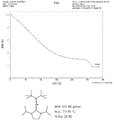
- 230000004580 weight loss Effects 0.000 description 25
- 239000000376 reactant Substances 0.000 description 23
- 125000001424 substituent group Chemical group 0.000 description 21
- CSCPPACGZOOCGX-UHFFFAOYSA-N Acetone Chemical compound CC(C)=O CSCPPACGZOOCGX-UHFFFAOYSA-N 0.000 description 20
- 229910021591 Copper(I) chloride Inorganic materials 0.000 description 20
- OXBLHERUFWYNTN-UHFFFAOYSA-M copper(I) chloride Chemical compound [Cu]Cl OXBLHERUFWYNTN-UHFFFAOYSA-M 0.000 description 20
- LFQSCWFLJHTTHZ-UHFFFAOYSA-N Ethanol Chemical compound CCO LFQSCWFLJHTTHZ-UHFFFAOYSA-N 0.000 description 19
- 239000013078 crystal Substances 0.000 description 19
- OFBQJSOFQDEBGM-UHFFFAOYSA-N n-pentane Natural products CCCCC OFBQJSOFQDEBGM-UHFFFAOYSA-N 0.000 description 19
- 239000000725 suspension Substances 0.000 description 19
- 239000003039 volatile agent Substances 0.000 description 17
- 239000012691 Cu precursor Substances 0.000 description 16
- 239000012159 carrier gas Substances 0.000 description 14
- 239000000706 filtrate Substances 0.000 description 14
- YNESATAKKCNGOF-UHFFFAOYSA-N lithium bis(trimethylsilyl)amide Chemical compound [Li+].C[Si](C)(C)[N-][Si](C)(C)C YNESATAKKCNGOF-UHFFFAOYSA-N 0.000 description 14
- YLQBMQCUIZJEEH-UHFFFAOYSA-N tetrahydrofuran Natural products C=1C=COC=1 YLQBMQCUIZJEEH-UHFFFAOYSA-N 0.000 description 14
- 238000005240 physical vapour deposition Methods 0.000 description 12
- 239000000047 product Substances 0.000 description 12
- MFRIHAYPQRLWNB-UHFFFAOYSA-N sodium tert-butoxide Chemical compound [Na+].CC(C)(C)[O-] MFRIHAYPQRLWNB-UHFFFAOYSA-N 0.000 description 12
- 239000002904 solvent Substances 0.000 description 12
- 238000002411 thermogravimetry Methods 0.000 description 12
- VEXZGXHMUGYJMC-UHFFFAOYSA-N Hydrochloric acid Chemical compound Cl VEXZGXHMUGYJMC-UHFFFAOYSA-N 0.000 description 11
- UTQPYFQVJZORSD-UHFFFAOYSA-N copper bis(trimethylsilyl)azanide Chemical compound [Cu+2].C[Si](C)(C)[N-][Si](C)(C)C.C[Si](C)(C)[N-][Si](C)(C)C UTQPYFQVJZORSD-UHFFFAOYSA-N 0.000 description 11
- 238000002474 experimental method Methods 0.000 description 11
- 238000000655 nuclear magnetic resonance spectrum Methods 0.000 description 11
- 238000010586 diagram Methods 0.000 description 10
- BASFCYQUMIYNBI-UHFFFAOYSA-N platinum Chemical compound [Pt] BASFCYQUMIYNBI-UHFFFAOYSA-N 0.000 description 10
- 238000012545 processing Methods 0.000 description 10
- YMWUJEATGCHHMB-UHFFFAOYSA-N Dichloromethane Chemical compound ClCCl YMWUJEATGCHHMB-UHFFFAOYSA-N 0.000 description 9
- 239000011261 inert gas Substances 0.000 description 9
- 239000007788 liquid Substances 0.000 description 9
- VLKZOEOYAKHREP-UHFFFAOYSA-N n-Hexane Chemical compound CCCCCC VLKZOEOYAKHREP-UHFFFAOYSA-N 0.000 description 9
- 239000012299 nitrogen atmosphere Substances 0.000 description 9
- 230000008859 change Effects 0.000 description 8
- 238000002447 crystallographic data Methods 0.000 description 8
- 239000000126 substance Substances 0.000 description 8
- WUHBJMXQJSWAGH-UHFFFAOYSA-M 1,3-di(propan-2-yl)-4,5-dihydroimidazol-1-ium;chloride Chemical compound [Cl-].CC(C)N1CC[N+](C(C)C)=C1 WUHBJMXQJSWAGH-UHFFFAOYSA-M 0.000 description 7
- OKTJSMMVPCPJKN-UHFFFAOYSA-N Carbon Chemical compound [C] OKTJSMMVPCPJKN-UHFFFAOYSA-N 0.000 description 7
- VEXZGXHMUGYJMC-UHFFFAOYSA-M Chloride anion Chemical compound [Cl-] VEXZGXHMUGYJMC-UHFFFAOYSA-M 0.000 description 7
- 230000001133 acceleration Effects 0.000 description 7
- 125000004429 atom Chemical group 0.000 description 7
- ORTQZVOHEJQUHG-UHFFFAOYSA-L copper(II) chloride Chemical class Cl[Cu]Cl ORTQZVOHEJQUHG-UHFFFAOYSA-L 0.000 description 7
- 238000013480 data collection Methods 0.000 description 7
- 230000009257 reactivity Effects 0.000 description 7
- 238000003756 stirring Methods 0.000 description 7
- 238000000859 sublimation Methods 0.000 description 7
- 230000008022 sublimation Effects 0.000 description 7
- RAOIDOHSFRTOEL-UHFFFAOYSA-N tetrahydrothiophene Chemical compound C1CCSC1 RAOIDOHSFRTOEL-UHFFFAOYSA-N 0.000 description 7
- 229910018072 Al 2 O 3 Inorganic materials 0.000 description 6
- OYDRJSYCABOKLS-UHFFFAOYSA-N C[Si](C)(C)[N-][Si](C)(C)C.CC(C)N1CCN(C(C)C)C1=[Au+] Chemical compound C[Si](C)(C)[N-][Si](C)(C)C.CC(C)N1CCN(C(C)C)C1=[Au+] OYDRJSYCABOKLS-UHFFFAOYSA-N 0.000 description 6
- GLQWTRIFTMPCDL-UHFFFAOYSA-N C[Si](C)(C)[N-][Si](C)(C)C.CCN1CCN(CC)C1=[Cu+] Chemical compound C[Si](C)(C)[N-][Si](C)(C)C.CCN1CCN(CC)C1=[Cu+] GLQWTRIFTMPCDL-UHFFFAOYSA-N 0.000 description 6
- 239000005749 Copper compound Substances 0.000 description 6
- UHOVQNZJYSORNB-MZWXYZOWSA-N benzene-d6 Chemical compound [2H]C1=C([2H])C([2H])=C([2H])C([2H])=C1[2H] UHOVQNZJYSORNB-MZWXYZOWSA-N 0.000 description 6
- WPYMKLBDIGXBTP-UHFFFAOYSA-N benzoic acid Chemical compound OC(=O)C1=CC=CC=C1 WPYMKLBDIGXBTP-UHFFFAOYSA-N 0.000 description 6
- 239000003153 chemical reaction reagent Substances 0.000 description 6
- 150000001880 copper compounds Chemical class 0.000 description 6
- 150000004820 halides Chemical class 0.000 description 6
- 239000003921 oil Substances 0.000 description 6
- 235000019198 oils Nutrition 0.000 description 6
- 238000010521 absorption reaction Methods 0.000 description 5
- 238000000354 decomposition reaction Methods 0.000 description 5
- 150000004985 diamines Chemical class 0.000 description 5
- 239000012535 impurity Substances 0.000 description 5
- 239000000543 intermediate Substances 0.000 description 5
- 150000002500 ions Chemical class 0.000 description 5
- 239000012528 membrane Substances 0.000 description 5
- 229910052697 platinum Inorganic materials 0.000 description 5
- 238000002360 preparation method Methods 0.000 description 5
- 238000001228 spectrum Methods 0.000 description 5
- AEVBPXDFDKBGLT-YOUFYPILSA-N (2s,3s,4r,5r)-n-[2-[4-(diethoxyphosphorylmethyl)anilino]-2-oxoethyl]-5-(2,4-dioxopyrimidin-1-yl)-3,4-dihydroxyoxolane-2-carboxamide Chemical compound C1=CC(CP(=O)(OCC)OCC)=CC=C1NC(=O)CNC(=O)[C@@H]1[C@@H](O)[C@@H](O)[C@H](N2C(NC(=O)C=C2)=O)O1 AEVBPXDFDKBGLT-YOUFYPILSA-N 0.000 description 4
- IKULNZRVXMLVMK-UHFFFAOYSA-M 1,3-diethyl-4,5-dihydroimidazol-1-ium;chloride Chemical compound [Cl-].CCN1CC[N+](CC)=C1 IKULNZRVXMLVMK-UHFFFAOYSA-M 0.000 description 4
- WGABOZPQOOZAOI-UHFFFAOYSA-N 2-[4-[[(3,5-dimethoxy-4-methylbenzoyl)-(3-phenylpropyl)amino]methyl]phenyl]acetic acid Chemical compound COC1=C(C)C(OC)=CC(C(=O)N(CCCC=2C=CC=CC=2)CC=2C=CC(CC(O)=O)=CC=2)=C1 WGABOZPQOOZAOI-UHFFFAOYSA-N 0.000 description 4
- LVBSJTOXNPVARB-UHFFFAOYSA-N C[Si](C)(C)[N-][Si](C)(C)C.CC(C)N1C(C)=C(C)N(C(C)C)C1=[Cu+] Chemical compound C[Si](C)(C)[N-][Si](C)(C)C.CC(C)N1C(C)=C(C)N(C(C)C)C1=[Cu+] LVBSJTOXNPVARB-UHFFFAOYSA-N 0.000 description 4
- VMQMZMRVKUZKQL-UHFFFAOYSA-N Cu+ Chemical compound [Cu+] VMQMZMRVKUZKQL-UHFFFAOYSA-N 0.000 description 4
- FAPWRFPIFSIZLT-UHFFFAOYSA-M Sodium chloride Chemical compound [Na+].[Cl-] FAPWRFPIFSIZLT-UHFFFAOYSA-M 0.000 description 4
- 125000003342 alkenyl group Chemical group 0.000 description 4
- 125000000304 alkynyl group Chemical group 0.000 description 4
- 238000004458 analytical method Methods 0.000 description 4
- 239000011248 coating agent Substances 0.000 description 4
- 238000000576 coating method Methods 0.000 description 4
- 229940126212 compound 17a Drugs 0.000 description 4
- 238000004821 distillation Methods 0.000 description 4
- 238000000635 electron micrograph Methods 0.000 description 4
- 238000011049 filling Methods 0.000 description 4
- 230000006872 improvement Effects 0.000 description 4
- HVTICUPFWKNHNG-UHFFFAOYSA-N iodoethane Chemical compound CCI HVTICUPFWKNHNG-UHFFFAOYSA-N 0.000 description 4
- BIFJXHQPKDLWIE-UHFFFAOYSA-N n,n'-diethylethane-1,2-diamine;dihydrochloride Chemical compound Cl.Cl.CCNCCNCC BIFJXHQPKDLWIE-UHFFFAOYSA-N 0.000 description 4
- 238000000425 proton nuclear magnetic resonance spectrum Methods 0.000 description 4
- 238000010992 reflux Methods 0.000 description 4
- 241000894007 species Species 0.000 description 4
- 230000009897 systematic effect Effects 0.000 description 4
- PYOKUURKVVELLB-UHFFFAOYSA-N trimethyl orthoformate Chemical compound COC(OC)OC PYOKUURKVVELLB-UHFFFAOYSA-N 0.000 description 4
- WCDLCPLAAKUJNY-UHFFFAOYSA-N 4-[4-[3-(1h-pyrazol-4-yl)pyrazolo[1,5-a]pyrimidin-6-yl]phenyl]morpholine Chemical compound C1COCCN1C1=CC=C(C2=CN3N=CC(=C3N=C2)C2=CNN=C2)C=C1 WCDLCPLAAKUJNY-UHFFFAOYSA-N 0.000 description 3
- ADLVDYMTBOSDFE-UHFFFAOYSA-N 5-chloro-6-nitroisoindole-1,3-dione Chemical compound C1=C(Cl)C([N+](=O)[O-])=CC2=C1C(=O)NC2=O ADLVDYMTBOSDFE-UHFFFAOYSA-N 0.000 description 3
- 239000005711 Benzoic acid Substances 0.000 description 3
- NDMPOVNGHDNXBH-UHFFFAOYSA-N C[Si](C)(C)[N-][Si](C)(C)C.CC(C)(C)N1C=CN(C(C)(C)C)C1=[Cu+] Chemical compound C[Si](C)(C)[N-][Si](C)(C)C.CC(C)(C)N1C=CN(C(C)(C)C)C1=[Cu+] NDMPOVNGHDNXBH-UHFFFAOYSA-N 0.000 description 3
- CURLTUGMZLYLDI-UHFFFAOYSA-N Carbon dioxide Chemical compound O=C=O CURLTUGMZLYLDI-UHFFFAOYSA-N 0.000 description 3
- ZMXDDKWLCZADIW-UHFFFAOYSA-N N,N-Dimethylformamide Chemical compound CN(C)C=O ZMXDDKWLCZADIW-UHFFFAOYSA-N 0.000 description 3
- RWRDLPDLKQPQOW-UHFFFAOYSA-N Pyrrolidine Chemical compound C1CCNC1 RWRDLPDLKQPQOW-UHFFFAOYSA-N 0.000 description 3
- YLEIFZAVNWDOBM-ZTNXSLBXSA-N ac1l9hc7 Chemical compound C([C@H]12)C[C@@H](C([C@@H](O)CC3)(C)C)[C@@]43C[C@@]14CC[C@@]1(C)[C@@]2(C)C[C@@H]2O[C@]3(O)[C@H](O)C(C)(C)O[C@@H]3[C@@H](C)[C@H]12 YLEIFZAVNWDOBM-ZTNXSLBXSA-N 0.000 description 3
- 229910052782 aluminium Inorganic materials 0.000 description 3
- XAGFODPZIPBFFR-UHFFFAOYSA-N aluminium Chemical compound [Al] XAGFODPZIPBFFR-UHFFFAOYSA-N 0.000 description 3
- 235000010233 benzoic acid Nutrition 0.000 description 3
- XGIUDIMNNMKGDE-UHFFFAOYSA-N bis(trimethylsilyl)azanide Chemical compound C[Si](C)(C)[N-][Si](C)(C)C XGIUDIMNNMKGDE-UHFFFAOYSA-N 0.000 description 3
- 125000004432 carbon atom Chemical group C* 0.000 description 3
- 235000011089 carbon dioxide Nutrition 0.000 description 3
- 238000005137 deposition process Methods 0.000 description 3
- 238000013461 design Methods 0.000 description 3
- UAOMVDZJSHZZME-UHFFFAOYSA-N diisopropylamine Chemical compound CC(C)NC(C)C UAOMVDZJSHZZME-UHFFFAOYSA-N 0.000 description 3
- BPBLGCSAYMJJJW-UHFFFAOYSA-M dimethylaminomethylidene(dimethyl)azanium;chloride Chemical compound [Cl-].CN(C)C=[N+](C)C BPBLGCSAYMJJJW-UHFFFAOYSA-M 0.000 description 3
- 239000012530 fluid Substances 0.000 description 3
- 125000005842 heteroatom Chemical group 0.000 description 3
- 150000002430 hydrocarbons Chemical group 0.000 description 3
- 150000002431 hydrogen Chemical class 0.000 description 3
- RAXXELZNTBOGNW-UHFFFAOYSA-N imidazole Natural products C1=CNC=N1 RAXXELZNTBOGNW-UHFFFAOYSA-N 0.000 description 3
- 238000002955 isolation Methods 0.000 description 3
- 239000011777 magnesium Substances 0.000 description 3
- 238000001000 micrograph Methods 0.000 description 3
- 238000005459 micromachining Methods 0.000 description 3
- MFIGJRRHGZYPDD-UHFFFAOYSA-N n,n'-di(propan-2-yl)ethane-1,2-diamine Chemical compound CC(C)NCCNC(C)C MFIGJRRHGZYPDD-UHFFFAOYSA-N 0.000 description 3
- 125000004433 nitrogen atom Chemical group N* 0.000 description 3
- 125000006574 non-aromatic ring group Chemical group 0.000 description 3
- 238000001208 nuclear magnetic resonance pulse sequence Methods 0.000 description 3
- 238000007747 plating Methods 0.000 description 3
- LPNYRYFBWFDTMA-UHFFFAOYSA-N potassium tert-butoxide Chemical compound [K+].CC(C)(C)[O-] LPNYRYFBWFDTMA-UHFFFAOYSA-N 0.000 description 3
- 239000000843 powder Substances 0.000 description 3
- 239000002244 precipitate Substances 0.000 description 3
- 239000012088 reference solution Substances 0.000 description 3
- 238000004544 sputter deposition Methods 0.000 description 3
- 239000007858 starting material Substances 0.000 description 3
- 238000000427 thin-film deposition Methods 0.000 description 3
- 238000007740 vapor deposition Methods 0.000 description 3
- ZCYVEMRRCGMTRW-UHFFFAOYSA-N 7553-56-2 Chemical group [I] ZCYVEMRRCGMTRW-UHFFFAOYSA-N 0.000 description 2
- NFIDSENWEVPGCL-UHFFFAOYSA-N CC(C)N(CCN1C(C)C)C1=[Ag].C[Si](C)(C)N[Si](C)(C)C Chemical compound CC(C)N(CCN1C(C)C)C1=[Ag].C[Si](C)(C)N[Si](C)(C)C NFIDSENWEVPGCL-UHFFFAOYSA-N 0.000 description 2
- QUSNBJAOOMFDIB-UHFFFAOYSA-N Ethylamine Chemical compound CCN QUSNBJAOOMFDIB-UHFFFAOYSA-N 0.000 description 2
- ZRALSGWEFCBTJO-UHFFFAOYSA-N Guanidine Chemical compound NC(N)=N ZRALSGWEFCBTJO-UHFFFAOYSA-N 0.000 description 2
- BAVYZALUXZFZLV-UHFFFAOYSA-N Methylamine Chemical compound NC BAVYZALUXZFZLV-UHFFFAOYSA-N 0.000 description 2
- CJKRXEBLWJVYJD-UHFFFAOYSA-N N,N'-diethylethylenediamine Chemical compound CCNCCNCC CJKRXEBLWJVYJD-UHFFFAOYSA-N 0.000 description 2
- IMNFDUFMRHMDMM-UHFFFAOYSA-N N-Heptane Chemical compound CCCCCCC IMNFDUFMRHMDMM-UHFFFAOYSA-N 0.000 description 2
- 235000019502 Orange oil Nutrition 0.000 description 2
- 229910019142 PO4 Inorganic materials 0.000 description 2
- 239000005662 Paraffin oil Substances 0.000 description 2
- NQRYJNQNLNOLGT-UHFFFAOYSA-N Piperidine Chemical compound C1CCNCC1 NQRYJNQNLNOLGT-UHFFFAOYSA-N 0.000 description 2
- 229910021607 Silver chloride Inorganic materials 0.000 description 2
- NIOLVNVKXOEOKS-UHFFFAOYSA-M [di(propan-2-yl)amino]methylidene-di(propan-2-yl)azanium;chloride Chemical compound [Cl-].CC(C)N(C(C)C)C=[N+](C(C)C)C(C)C NIOLVNVKXOEOKS-UHFFFAOYSA-M 0.000 description 2
- 230000002776 aggregation Effects 0.000 description 2
- 125000003545 alkoxy group Chemical group 0.000 description 2
- 150000001540 azides Chemical class 0.000 description 2
- 239000003054 catalyst Substances 0.000 description 2
- 238000012512 characterization method Methods 0.000 description 2
- 239000004020 conductor Substances 0.000 description 2
- 238000012937 correction Methods 0.000 description 2
- 238000013211 curve analysis Methods 0.000 description 2
- 239000000539 dimer Substances 0.000 description 2
- 238000005516 engineering process Methods 0.000 description 2
- 238000001704 evaporation Methods 0.000 description 2
- 230000008020 evaporation Effects 0.000 description 2
- 238000001914 filtration Methods 0.000 description 2
- 239000011888 foil Substances 0.000 description 2
- 235000013305 food Nutrition 0.000 description 2
- 239000003365 glass fiber Substances 0.000 description 2
- 150000002344 gold compounds Chemical class 0.000 description 2
- NEXSMEBSBIABKL-UHFFFAOYSA-N hexamethyldisilane Chemical compound C[Si](C)(C)[Si](C)(C)C NEXSMEBSBIABKL-UHFFFAOYSA-N 0.000 description 2
- 238000009616 inductively coupled plasma Methods 0.000 description 2
- 230000003993 interaction Effects 0.000 description 2
- 230000009878 intermolecular interaction Effects 0.000 description 2
- 238000003475 lamination Methods 0.000 description 2
- 239000012705 liquid precursor Substances 0.000 description 2
- 230000004807 localization Effects 0.000 description 2
- 238000005259 measurement Methods 0.000 description 2
- 230000007246 mechanism Effects 0.000 description 2
- 229910052987 metal hydride Inorganic materials 0.000 description 2
- 150000004681 metal hydrides Chemical class 0.000 description 2
- VNWKTOKETHGBQD-UHFFFAOYSA-N methane Chemical compound C VNWKTOKETHGBQD-UHFFFAOYSA-N 0.000 description 2
- 230000004048 modification Effects 0.000 description 2
- 238000012986 modification Methods 0.000 description 2
- 239000002808 molecular sieve Substances 0.000 description 2
- LOGIFHDKSCXBAC-UHFFFAOYSA-N n,n'-di(propan-2-yl)ethane-1,2-diamine;dihydrochloride Chemical compound Cl.Cl.CC(C)NCCNC(C)C LOGIFHDKSCXBAC-UHFFFAOYSA-N 0.000 description 2
- DBQQUTSEQPPYPO-UHFFFAOYSA-N n,n'-ditert-butylethane-1,2-diamine;dihydrochloride Chemical compound Cl.Cl.CC(C)(C)NCCNC(C)(C)C DBQQUTSEQPPYPO-UHFFFAOYSA-N 0.000 description 2
- 239000002159 nanocrystal Substances 0.000 description 2
- 238000005457 optimization Methods 0.000 description 2
- 239000010502 orange oil Substances 0.000 description 2
- 125000004430 oxygen atom Chemical group O* 0.000 description 2
- 230000037361 pathway Effects 0.000 description 2
- 239000010452 phosphate Substances 0.000 description 2
- XHXFXVLFKHQFAL-UHFFFAOYSA-N phosphoryl trichloride Chemical compound ClP(Cl)(Cl)=O XHXFXVLFKHQFAL-UHFFFAOYSA-N 0.000 description 2
- 238000005498 polishing Methods 0.000 description 2
- 239000005373 porous glass Substances 0.000 description 2
- 239000011148 porous material Substances 0.000 description 2
- 238000002203 pretreatment Methods 0.000 description 2
- 238000000746 purification Methods 0.000 description 2
- 238000011160 research Methods 0.000 description 2
- HKZLPVFGJNLROG-UHFFFAOYSA-M silver monochloride Chemical compound [Cl-].[Ag+] HKZLPVFGJNLROG-UHFFFAOYSA-M 0.000 description 2
- 239000002002 slurry Substances 0.000 description 2
- URGAHOPLAPQHLN-UHFFFAOYSA-N sodium aluminosilicate Chemical compound [Na+].[Al+3].[O-][Si]([O-])=O.[O-][Si]([O-])=O URGAHOPLAPQHLN-UHFFFAOYSA-N 0.000 description 2
- WRIKHQLVHPKCJU-UHFFFAOYSA-N sodium bis(trimethylsilyl)amide Chemical compound C[Si](C)(C)N([Na])[Si](C)(C)C WRIKHQLVHPKCJU-UHFFFAOYSA-N 0.000 description 2
- 239000011780 sodium chloride Substances 0.000 description 2
- 239000006228 supernatant Substances 0.000 description 2
- 238000010189 synthetic method Methods 0.000 description 2
- MZLGASXMSKOWSE-UHFFFAOYSA-N tantalum nitride Chemical compound [Ta]#N MZLGASXMSKOWSE-UHFFFAOYSA-N 0.000 description 2
- 229940071240 tetrachloroaurate Drugs 0.000 description 2
- 230000008646 thermal stress Effects 0.000 description 2
- FYSNRJHAOHDILO-UHFFFAOYSA-N thionyl chloride Chemical compound ClS(Cl)=O FYSNRJHAOHDILO-UHFFFAOYSA-N 0.000 description 2
- 229910052723 transition metal Inorganic materials 0.000 description 2
- 150000003624 transition metals Chemical class 0.000 description 2
- GKASDNZWUGIAMG-UHFFFAOYSA-N triethyl orthoformate Chemical compound CCOC(OCC)OCC GKASDNZWUGIAMG-UHFFFAOYSA-N 0.000 description 2
- 125000000026 trimethylsilyl group Chemical group [H]C([H])([H])[Si]([*])(C([H])([H])[H])C([H])([H])[H] 0.000 description 2
- 238000012982 x-ray structure analysis Methods 0.000 description 2
- VWQHBWVJAVTWQG-UHFFFAOYSA-M 1,3-ditert-butyl-4,5-dihydroimidazol-1-ium;chloride Chemical compound [Cl-].CC(C)(C)N1CC[N+](C(C)(C)C)=C1 VWQHBWVJAVTWQG-UHFFFAOYSA-M 0.000 description 1
- RYHBNJHYFVUHQT-UHFFFAOYSA-N 1,4-Dioxane Chemical compound C1COCCO1 RYHBNJHYFVUHQT-UHFFFAOYSA-N 0.000 description 1
- VRIMBAGMCFLRRY-UHFFFAOYSA-M 1-tert-butyl-3-ethyl-4,5-dihydroimidazol-3-ium;chloride Chemical compound [Cl-].CCN1CC[N+](C(C)(C)C)=C1 VRIMBAGMCFLRRY-UHFFFAOYSA-M 0.000 description 1
- CJINLWNKOZBXMF-UHFFFAOYSA-M 1-tert-butyl-3-methyl-4,5-dihydroimidazol-3-ium;chloride Chemical compound [Cl-].CN1CC[N+](C(C)(C)C)=C1 CJINLWNKOZBXMF-UHFFFAOYSA-M 0.000 description 1
- DCPXDNQTCUBMHS-UHFFFAOYSA-M 1-tert-butyl-3-propan-2-yl-4,5-dihydroimidazol-3-ium;chloride Chemical compound [Cl-].CC(C)N1CC[N+](C(C)(C)C)=C1 DCPXDNQTCUBMHS-UHFFFAOYSA-M 0.000 description 1
- JDIIGWSSTNUWGK-UHFFFAOYSA-N 1h-imidazol-3-ium;chloride Chemical compound [Cl-].[NH2+]1C=CN=C1 JDIIGWSSTNUWGK-UHFFFAOYSA-N 0.000 description 1
- IUXYVKZUDNLISR-UHFFFAOYSA-N 2-(tert-butylamino)ethanol Chemical compound CC(C)(C)NCCO IUXYVKZUDNLISR-UHFFFAOYSA-N 0.000 description 1
- BJAYKVGFRDEELV-UHFFFAOYSA-N 2-propyl-4,5-dihydro-1H-imidazole hydrochloride Chemical compound Cl.C(CC)C=1NCCN1 BJAYKVGFRDEELV-UHFFFAOYSA-N 0.000 description 1
- MCSXGCZMEPXKIW-UHFFFAOYSA-N 3-hydroxy-4-[(4-methyl-2-nitrophenyl)diazenyl]-N-(3-nitrophenyl)naphthalene-2-carboxamide Chemical compound Cc1ccc(N=Nc2c(O)c(cc3ccccc23)C(=O)Nc2cccc(c2)[N+]([O-])=O)c(c1)[N+]([O-])=O MCSXGCZMEPXKIW-UHFFFAOYSA-N 0.000 description 1
- UFQDKRWQSFLPQY-UHFFFAOYSA-N 4,5-dihydro-1h-imidazol-3-ium;chloride Chemical compound Cl.C1CN=CN1 UFQDKRWQSFLPQY-UHFFFAOYSA-N 0.000 description 1
- QCMHGCDOZLWPOT-FMNCTDSISA-N COC1=C(CC[C@@H]2CCC3=C(C2)C=CC(=C3)[C@H]2CC[C@](N)(CO)C2)C=CC=C1 Chemical compound COC1=C(CC[C@@H]2CCC3=C(C2)C=CC(=C3)[C@H]2CC[C@](N)(CO)C2)C=CC=C1 QCMHGCDOZLWPOT-FMNCTDSISA-N 0.000 description 1
- UJHYABXBRZBYHR-UHFFFAOYSA-N C[Si](C)(C)[N-][Si](C)(C)C.CC(C)(C)N1CCN(C(C)(C)C)C1=[Cu+] Chemical compound C[Si](C)(C)[N-][Si](C)(C)C.CC(C)(C)N1CCN(C(C)(C)C)C1=[Cu+] UJHYABXBRZBYHR-UHFFFAOYSA-N 0.000 description 1
- PCUDNNQTYAKKOJ-UHFFFAOYSA-N C[Si](C)(C)[N-][Si](C)(C)C.CC(C)N1CCN(C(C)(C)C)C1=[Cu+] Chemical compound C[Si](C)(C)[N-][Si](C)(C)C.CC(C)N1CCN(C(C)(C)C)C1=[Cu+] PCUDNNQTYAKKOJ-UHFFFAOYSA-N 0.000 description 1
- UKEWWDKPRXIECB-UHFFFAOYSA-N C[Si](C)(C)[N-][Si](C)(C)C.CC1C(C)N(C(C)(C)C)C(=[Cu+])N1C(C)(C)C Chemical compound C[Si](C)(C)[N-][Si](C)(C)C.CC1C(C)N(C(C)(C)C)C(=[Cu+])N1C(C)(C)C UKEWWDKPRXIECB-UHFFFAOYSA-N 0.000 description 1
- LUBUQDJKFYTISD-UHFFFAOYSA-N C[Si](C)(C)[N-][Si](C)(C)C.CCN1CCN(C(C)(C)C)C1=[Cu+] Chemical compound C[Si](C)(C)[N-][Si](C)(C)C.CCN1CCN(C(C)(C)C)C1=[Cu+] LUBUQDJKFYTISD-UHFFFAOYSA-N 0.000 description 1
- YHVVNKZJCOUQJR-UHFFFAOYSA-N C[Si](C)(C)[N-][Si](C)(C)C.CN1CCN(C(C)(C)C)C1=[Cu+] Chemical compound C[Si](C)(C)[N-][Si](C)(C)C.CN1CCN(C(C)(C)C)C1=[Cu+] YHVVNKZJCOUQJR-UHFFFAOYSA-N 0.000 description 1
- BVKZGUZCCUSVTD-UHFFFAOYSA-L Carbonate Chemical compound [O-]C([O-])=O BVKZGUZCCUSVTD-UHFFFAOYSA-L 0.000 description 1
- JZUFKLXOESDKRF-UHFFFAOYSA-N Chlorothiazide Chemical compound C1=C(Cl)C(S(=O)(=O)N)=CC2=C1NCNS2(=O)=O JZUFKLXOESDKRF-UHFFFAOYSA-N 0.000 description 1
- QBXVXKRWOVBUDB-GRKNLSHJSA-N ClC=1C(=CC(=C(CN2[C@H](C[C@H](C2)O)C(=O)O)C1)OCC1=CC(=CC=C1)C#N)OCC1=C(C(=CC=C1)C1=CC2=C(OCCO2)C=C1)C Chemical compound ClC=1C(=CC(=C(CN2[C@H](C[C@H](C2)O)C(=O)O)C1)OCC1=CC(=CC=C1)C#N)OCC1=C(C(=CC=C1)C1=CC2=C(OCCO2)C=C1)C QBXVXKRWOVBUDB-GRKNLSHJSA-N 0.000 description 1
- HMZGOVWVHDXZHK-UHFFFAOYSA-M Cl[Cu]=C1NCCN1 Chemical compound Cl[Cu]=C1NCCN1 HMZGOVWVHDXZHK-UHFFFAOYSA-M 0.000 description 1
- 235000013175 Crataegus laevigata Nutrition 0.000 description 1
- 229910002480 Cu-O Inorganic materials 0.000 description 1
- 229910002530 Cu-Y Inorganic materials 0.000 description 1
- YIIMEMSDCNDGTB-UHFFFAOYSA-N Dimethylcarbamoyl chloride Chemical compound CN(C)C(Cl)=O YIIMEMSDCNDGTB-UHFFFAOYSA-N 0.000 description 1
- PIICEJLVQHRZGT-UHFFFAOYSA-N Ethylenediamine Chemical compound NCCN PIICEJLVQHRZGT-UHFFFAOYSA-N 0.000 description 1
- 241000976924 Inca Species 0.000 description 1
- FYYHWMGAXLPEAU-UHFFFAOYSA-N Magnesium Chemical compound [Mg] FYYHWMGAXLPEAU-UHFFFAOYSA-N 0.000 description 1
- 241001024304 Mino Species 0.000 description 1
- CHJJGSNFBQVOTG-UHFFFAOYSA-N N-methyl-guanidine Natural products CNC(N)=N CHJJGSNFBQVOTG-UHFFFAOYSA-N 0.000 description 1
- 229910002651 NO3 Inorganic materials 0.000 description 1
- NHNBFGGVMKEFGY-UHFFFAOYSA-N Nitrate Chemical compound [O-][N+]([O-])=O NHNBFGGVMKEFGY-UHFFFAOYSA-N 0.000 description 1
- 229910052777 Praseodymium Inorganic materials 0.000 description 1
- KEAYESYHFKHZAL-UHFFFAOYSA-N Sodium Chemical compound [Na] KEAYESYHFKHZAL-UHFFFAOYSA-N 0.000 description 1
- QAOWNCQODCNURD-UHFFFAOYSA-L Sulfate Chemical compound [O-]S([O-])(=O)=O QAOWNCQODCNURD-UHFFFAOYSA-L 0.000 description 1
- 229910004166 TaN Inorganic materials 0.000 description 1
- RTAQQCXQSZGOHL-UHFFFAOYSA-N Titanium Chemical compound [Ti] RTAQQCXQSZGOHL-UHFFFAOYSA-N 0.000 description 1
- 238000004125 X-ray microanalysis Methods 0.000 description 1
- 238000004833 X-ray photoelectron spectroscopy Methods 0.000 description 1
- QCWXUUIWCKQGHC-UHFFFAOYSA-N Zirconium Chemical compound [Zr] QCWXUUIWCKQGHC-UHFFFAOYSA-N 0.000 description 1
- PNXKRHWROOZWSO-UHFFFAOYSA-N [Si].[Ru] Chemical compound [Si].[Ru] PNXKRHWROOZWSO-UHFFFAOYSA-N 0.000 description 1
- 238000009825 accumulation Methods 0.000 description 1
- 125000004442 acylamino group Chemical group 0.000 description 1
- 230000000274 adsorptive effect Effects 0.000 description 1
- 238000005273 aeration Methods 0.000 description 1
- 239000000443 aerosol Substances 0.000 description 1
- 238000005054 agglomeration Methods 0.000 description 1
- 238000004220 aggregation Methods 0.000 description 1
- 150000001298 alcohols Chemical class 0.000 description 1
- 125000006323 alkenyl amino group Chemical group 0.000 description 1
- 125000004450 alkenylene group Chemical group 0.000 description 1
- 125000004453 alkoxycarbonyl group Chemical group 0.000 description 1
- 125000005194 alkoxycarbonyloxy group Chemical group 0.000 description 1
- 125000003282 alkyl amino group Chemical group 0.000 description 1
- 125000004448 alkyl carbonyl group Chemical group 0.000 description 1
- 125000005196 alkyl carbonyloxy group Chemical group 0.000 description 1
- 125000004691 alkyl thio carbonyl group Chemical group 0.000 description 1
- 125000004414 alkyl thio group Chemical group 0.000 description 1
- 125000002947 alkylene group Chemical group 0.000 description 1
- 229940059260 amidate Drugs 0.000 description 1
- 150000001409 amidines Chemical class 0.000 description 1
- NMVVJCLUYUWBSZ-UHFFFAOYSA-N aminomethylideneazanium;chloride Chemical compound Cl.NC=N NMVVJCLUYUWBSZ-UHFFFAOYSA-N 0.000 description 1
- 125000004397 aminosulfonyl group Chemical group NS(=O)(=O)* 0.000 description 1
- 150000001450 anions Chemical class 0.000 description 1
- 238000003556 assay Methods 0.000 description 1
- 125000000852 azido group Chemical group *N=[N+]=[N-] 0.000 description 1
- RWCCWEUUXYIKHB-UHFFFAOYSA-N benzophenone Chemical compound C=1C=CC=CC=1C(=O)C1=CC=CC=C1 RWCCWEUUXYIKHB-UHFFFAOYSA-N 0.000 description 1
- 239000012965 benzophenone Substances 0.000 description 1
- SEHPFYAPKAWFTN-UHFFFAOYSA-N bis(trimethylsilyl)azanide gold(1+) Chemical compound [Au+].C[Si](C)(C)[N-][Si](C)(C)C SEHPFYAPKAWFTN-UHFFFAOYSA-N 0.000 description 1
- 229910052797 bismuth Inorganic materials 0.000 description 1
- JCXGWMGPZLAOME-UHFFFAOYSA-N bismuth atom Chemical compound [Bi] JCXGWMGPZLAOME-UHFFFAOYSA-N 0.000 description 1
- 229910052794 bromium Inorganic materials 0.000 description 1
- 239000006227 byproduct Substances 0.000 description 1
- 125000003917 carbamoyl group Chemical group [H]N([H])C(*)=O 0.000 description 1
- 150000001721 carbon Chemical group 0.000 description 1
- 239000007795 chemical reaction product Substances 0.000 description 1
- 239000013626 chemical specie Substances 0.000 description 1
- 229910052801 chlorine Inorganic materials 0.000 description 1
- 230000000052 comparative effect Effects 0.000 description 1
- 230000009918 complex formation Effects 0.000 description 1
- 238000009833 condensation Methods 0.000 description 1
- 230000005494 condensation Effects 0.000 description 1
- 238000011109 contamination Methods 0.000 description 1
- 238000004320 controlled atmosphere Methods 0.000 description 1
- 239000012043 crude product Substances 0.000 description 1
- 125000004093 cyano group Chemical group *C#N 0.000 description 1
- 230000007423 decrease Effects 0.000 description 1
- 230000001934 delay Effects 0.000 description 1
- 230000001419 dependent effect Effects 0.000 description 1
- 238000003795 desorption Methods 0.000 description 1
- 125000005265 dialkylamine group Chemical group 0.000 description 1
- 238000009792 diffusion process Methods 0.000 description 1
- 229940043279 diisopropylamine Drugs 0.000 description 1
- SWSQBOPZIKWTGO-UHFFFAOYSA-N dimethylaminoamidine Natural products CN(C)C(N)=N SWSQBOPZIKWTGO-UHFFFAOYSA-N 0.000 description 1
- 229910001873 dinitrogen Inorganic materials 0.000 description 1
- 238000006073 displacement reaction Methods 0.000 description 1
- 238000001035 drying Methods 0.000 description 1
- 230000000694 effects Effects 0.000 description 1
- 150000002148 esters Chemical class 0.000 description 1
- 150000002170 ethers Chemical class 0.000 description 1
- NPUKDXXFDDZOKR-LLVKDONJSA-N etomidate Chemical compound CCOC(=O)C1=CN=CN1[C@H](C)C1=CC=CC=C1 NPUKDXXFDDZOKR-LLVKDONJSA-N 0.000 description 1
- 230000005284 excitation Effects 0.000 description 1
- 239000000284 extract Substances 0.000 description 1
- 229910052731 fluorine Inorganic materials 0.000 description 1
- 238000005187 foaming Methods 0.000 description 1
- WBJINCZRORDGAQ-UHFFFAOYSA-N formic acid ethyl ester Natural products CCOC=O WBJINCZRORDGAQ-UHFFFAOYSA-N 0.000 description 1
- 239000012634 fragment Substances 0.000 description 1
- 125000000524 functional group Chemical group 0.000 description 1
- 125000002541 furyl group Chemical group 0.000 description 1
- 238000010574 gas phase reaction Methods 0.000 description 1
- UCGCVRKULHHWGA-UHFFFAOYSA-M gold(1+);thiolane;chloride Chemical compound [Au]Cl.C1CCSC1 UCGCVRKULHHWGA-UHFFFAOYSA-M 0.000 description 1
- 229910052735 hafnium Inorganic materials 0.000 description 1
- VBJZVLUMGGDVMO-UHFFFAOYSA-N hafnium atom Chemical compound [Hf] VBJZVLUMGGDVMO-UHFFFAOYSA-N 0.000 description 1
- 229910052736 halogen Inorganic materials 0.000 description 1
- 150000002367 halogens Chemical class 0.000 description 1
- 150000004679 hydroxides Chemical class 0.000 description 1
- 125000002887 hydroxy group Chemical group [H]O* 0.000 description 1
- 150000004693 imidazolium salts Chemical class 0.000 description 1
- 238000002347 injection Methods 0.000 description 1
- 239000007924 injection Substances 0.000 description 1
- 239000011810 insulating material Substances 0.000 description 1
- 238000004573 interface analysis Methods 0.000 description 1
- 230000001788 irregular Effects 0.000 description 1
- 238000002032 lab-on-a-chip Methods 0.000 description 1
- 229910052746 lanthanum Inorganic materials 0.000 description 1
- FZLIPJUXYLNCLC-UHFFFAOYSA-N lanthanum atom Chemical compound [La] FZLIPJUXYLNCLC-UHFFFAOYSA-N 0.000 description 1
- 239000011133 lead Substances 0.000 description 1
- 229910003002 lithium salt Inorganic materials 0.000 description 1
- 159000000002 lithium salts Chemical class 0.000 description 1
- 229910052749 magnesium Inorganic materials 0.000 description 1
- WPBNNNQJVZRUHP-UHFFFAOYSA-L manganese(2+);methyl n-[[2-(methoxycarbonylcarbamothioylamino)phenyl]carbamothioyl]carbamate;n-[2-(sulfidocarbothioylamino)ethyl]carbamodithioate Chemical compound [Mn+2].[S-]C(=S)NCCNC([S-])=S.COC(=O)NC(=S)NC1=CC=CC=C1NC(=S)NC(=O)OC WPBNNNQJVZRUHP-UHFFFAOYSA-L 0.000 description 1
- 239000011159 matrix material Substances 0.000 description 1
- 229910044991 metal oxide Inorganic materials 0.000 description 1
- 150000004706 metal oxides Chemical class 0.000 description 1
- CLKUPZYLSZLSSN-UHFFFAOYSA-N methylidenecopper Chemical compound [Cu]=C CLKUPZYLSZLSSN-UHFFFAOYSA-N 0.000 description 1
- 230000005012 migration Effects 0.000 description 1
- 238000013508 migration Methods 0.000 description 1
- 238000002156 mixing Methods 0.000 description 1
- 239000002052 molecular layer Substances 0.000 description 1
- PDXKMDGONYRVES-UHFFFAOYSA-N n,n',n'-tributylethane-1,2-diamine Chemical compound CCCCNCCN(CCCC)CCCC PDXKMDGONYRVES-UHFFFAOYSA-N 0.000 description 1
- KGHYGBGIWLNFAV-UHFFFAOYSA-N n,n'-ditert-butylethane-1,2-diamine Chemical compound CC(C)(C)NCCNC(C)(C)C KGHYGBGIWLNFAV-UHFFFAOYSA-N 0.000 description 1
- UNBDDZDKBWPHAX-UHFFFAOYSA-N n,n-di(propan-2-yl)formamide Chemical compound CC(C)N(C=O)C(C)C UNBDDZDKBWPHAX-UHFFFAOYSA-N 0.000 description 1
- 239000002086 nanomaterial Substances 0.000 description 1
- 230000007935 neutral effect Effects 0.000 description 1
- 229910052758 niobium Inorganic materials 0.000 description 1
- 239000010955 niobium Substances 0.000 description 1
- GUCVJGMIXFAOAE-UHFFFAOYSA-N niobium atom Chemical compound [Nb] GUCVJGMIXFAOAE-UHFFFAOYSA-N 0.000 description 1
- 150000002825 nitriles Chemical class 0.000 description 1
- 125000000449 nitro group Chemical group [O-][N+](*)=O 0.000 description 1
- 229940054975 nitrogen 99.99 % Drugs 0.000 description 1
- 230000006911 nucleation Effects 0.000 description 1
- 238000010899 nucleation Methods 0.000 description 1
- 230000000269 nucleophilic effect Effects 0.000 description 1
- 230000003287 optical effect Effects 0.000 description 1
- 230000003647 oxidation Effects 0.000 description 1
- 238000007254 oxidation reaction Methods 0.000 description 1
- 238000004806 packaging method and process Methods 0.000 description 1
- 239000002245 particle Substances 0.000 description 1
- 230000000737 periodic effect Effects 0.000 description 1
- 239000012071 phase Substances 0.000 description 1
- 125000001997 phenyl group Chemical group [H]C1=C([H])C([H])=C(*)C([H])=C1[H] 0.000 description 1
- NBIIXXVUZAFLBC-UHFFFAOYSA-K phosphate Chemical compound [O-]P([O-])([O-])=O NBIIXXVUZAFLBC-UHFFFAOYSA-K 0.000 description 1
- UEZVMMHDMIWARA-UHFFFAOYSA-M phosphonate Chemical compound [O-]P(=O)=O UEZVMMHDMIWARA-UHFFFAOYSA-M 0.000 description 1
- 239000004033 plastic Substances 0.000 description 1
- 159000000001 potassium salts Chemical class 0.000 description 1
- PUDIUYLPXJFUGB-UHFFFAOYSA-N praseodymium atom Chemical compound [Pr] PUDIUYLPXJFUGB-UHFFFAOYSA-N 0.000 description 1
- 238000009417 prefabrication Methods 0.000 description 1
- 125000002924 primary amino group Chemical group [H]N([H])* 0.000 description 1
- 125000004076 pyridyl group Chemical group 0.000 description 1
- 239000011541 reaction mixture Substances 0.000 description 1
- 238000001953 recrystallisation Methods 0.000 description 1
- 230000009467 reduction Effects 0.000 description 1
- 239000013557 residual solvent Substances 0.000 description 1
- 238000005389 semiconductor device fabrication Methods 0.000 description 1
- 239000011343 solid material Substances 0.000 description 1
- 230000000087 stabilizing effect Effects 0.000 description 1
- 229910001220 stainless steel Inorganic materials 0.000 description 1
- 239000010935 stainless steel Substances 0.000 description 1
- 238000010561 standard procedure Methods 0.000 description 1
- 238000003860 storage Methods 0.000 description 1
- 238000012496 stress study Methods 0.000 description 1
- 229940124530 sulfonamide Drugs 0.000 description 1
- 150000003456 sulfonamides Chemical class 0.000 description 1
- BDHFUVZGWQCTTF-UHFFFAOYSA-M sulfonate Chemical compound [O-]S(=O)=O BDHFUVZGWQCTTF-UHFFFAOYSA-M 0.000 description 1
- 229910052717 sulfur Inorganic materials 0.000 description 1
- 238000005211 surface analysis Methods 0.000 description 1
- 238000006557 surface reaction Methods 0.000 description 1
- 238000001308 synthesis method Methods 0.000 description 1
- 229940066765 systemic antihistamines substituted ethylene diamines Drugs 0.000 description 1
- 238000007725 thermal activation Methods 0.000 description 1
- 238000005979 thermal decomposition reaction Methods 0.000 description 1
- 238000002207 thermal evaporation Methods 0.000 description 1
- 125000001544 thienyl group Chemical group 0.000 description 1
- 238000010896 thin film analysis Methods 0.000 description 1
- 150000007970 thio esters Chemical class 0.000 description 1
- 150000003568 thioethers Chemical class 0.000 description 1
- 229910052719 titanium Inorganic materials 0.000 description 1
- 239000010936 titanium Substances 0.000 description 1
- 239000012808 vapor phase Substances 0.000 description 1
- 238000010792 warming Methods 0.000 description 1
- 229910052726 zirconium Inorganic materials 0.000 description 1
Images


Classifications
-
- C—CHEMISTRY; METALLURGY
- C07—ORGANIC CHEMISTRY
- C07F—ACYCLIC, CARBOCYCLIC OR HETEROCYCLIC COMPOUNDS CONTAINING ELEMENTS OTHER THAN CARBON, HYDROGEN, HALOGEN, OXYGEN, NITROGEN, SULFUR, SELENIUM OR TELLURIUM
- C07F7/00—Compounds containing elements of Groups 4 or 14 of the Periodic Table
- C07F7/02—Silicon compounds
- C07F7/08—Compounds having one or more C—Si linkages
- C07F7/10—Compounds having one or more C—Si linkages containing nitrogen having a Si-N linkage
-
- C—CHEMISTRY; METALLURGY
- C07—ORGANIC CHEMISTRY
- C07F—ACYCLIC, CARBOCYCLIC OR HETEROCYCLIC COMPOUNDS CONTAINING ELEMENTS OTHER THAN CARBON, HYDROGEN, HALOGEN, OXYGEN, NITROGEN, SULFUR, SELENIUM OR TELLURIUM
- C07F1/00—Compounds containing elements of Groups 1 or 11 of the Periodic Table
-
- C—CHEMISTRY; METALLURGY
- C07—ORGANIC CHEMISTRY
- C07F—ACYCLIC, CARBOCYCLIC OR HETEROCYCLIC COMPOUNDS CONTAINING ELEMENTS OTHER THAN CARBON, HYDROGEN, HALOGEN, OXYGEN, NITROGEN, SULFUR, SELENIUM OR TELLURIUM
- C07F1/00—Compounds containing elements of Groups 1 or 11 of the Periodic Table
- C07F1/005—Compounds containing elements of Groups 1 or 11 of the Periodic Table without C-Metal linkages
-
- C—CHEMISTRY; METALLURGY
- C07—ORGANIC CHEMISTRY
- C07F—ACYCLIC, CARBOCYCLIC OR HETEROCYCLIC COMPOUNDS CONTAINING ELEMENTS OTHER THAN CARBON, HYDROGEN, HALOGEN, OXYGEN, NITROGEN, SULFUR, SELENIUM OR TELLURIUM
- C07F1/00—Compounds containing elements of Groups 1 or 11 of the Periodic Table
- C07F1/08—Copper compounds
-
- C—CHEMISTRY; METALLURGY
- C07—ORGANIC CHEMISTRY
- C07F—ACYCLIC, CARBOCYCLIC OR HETEROCYCLIC COMPOUNDS CONTAINING ELEMENTS OTHER THAN CARBON, HYDROGEN, HALOGEN, OXYGEN, NITROGEN, SULFUR, SELENIUM OR TELLURIUM
- C07F7/00—Compounds containing elements of Groups 4 or 14 of the Periodic Table
- C07F7/02—Silicon compounds
- C07F7/08—Compounds having one or more C—Si linkages
-
- C—CHEMISTRY; METALLURGY
- C09—DYES; PAINTS; POLISHES; NATURAL RESINS; ADHESIVES; COMPOSITIONS NOT OTHERWISE PROVIDED FOR; APPLICATIONS OF MATERIALS NOT OTHERWISE PROVIDED FOR
- C09D—COATING COMPOSITIONS, e.g. PAINTS, VARNISHES OR LACQUERS; FILLING PASTES; CHEMICAL PAINT OR INK REMOVERS; INKS; CORRECTING FLUIDS; WOODSTAINS; PASTES OR SOLIDS FOR COLOURING OR PRINTING; USE OF MATERIALS THEREFOR
- C09D5/00—Coating compositions, e.g. paints, varnishes or lacquers, characterised by their physical nature or the effects produced; Filling pastes
- C09D5/24—Electrically-conducting paints
-
- C—CHEMISTRY; METALLURGY
- C23—COATING METALLIC MATERIAL; COATING MATERIAL WITH METALLIC MATERIAL; CHEMICAL SURFACE TREATMENT; DIFFUSION TREATMENT OF METALLIC MATERIAL; COATING BY VACUUM EVAPORATION, BY SPUTTERING, BY ION IMPLANTATION OR BY CHEMICAL VAPOUR DEPOSITION, IN GENERAL; INHIBITING CORROSION OF METALLIC MATERIAL OR INCRUSTATION IN GENERAL
- C23C—COATING METALLIC MATERIAL; COATING MATERIAL WITH METALLIC MATERIAL; SURFACE TREATMENT OF METALLIC MATERIAL BY DIFFUSION INTO THE SURFACE, BY CHEMICAL CONVERSION OR SUBSTITUTION; COATING BY VACUUM EVAPORATION, BY SPUTTERING, BY ION IMPLANTATION OR BY CHEMICAL VAPOUR DEPOSITION, IN GENERAL
- C23C16/00—Chemical coating by decomposition of gaseous compounds, without leaving reaction products of surface material in the coating, i.e. chemical vapour deposition [CVD] processes
- C23C16/06—Chemical coating by decomposition of gaseous compounds, without leaving reaction products of surface material in the coating, i.e. chemical vapour deposition [CVD] processes characterised by the deposition of metallic material
- C23C16/18—Chemical coating by decomposition of gaseous compounds, without leaving reaction products of surface material in the coating, i.e. chemical vapour deposition [CVD] processes characterised by the deposition of metallic material from metallo-organic compounds
-
- C—CHEMISTRY; METALLURGY
- C23—COATING METALLIC MATERIAL; COATING MATERIAL WITH METALLIC MATERIAL; CHEMICAL SURFACE TREATMENT; DIFFUSION TREATMENT OF METALLIC MATERIAL; COATING BY VACUUM EVAPORATION, BY SPUTTERING, BY ION IMPLANTATION OR BY CHEMICAL VAPOUR DEPOSITION, IN GENERAL; INHIBITING CORROSION OF METALLIC MATERIAL OR INCRUSTATION IN GENERAL
- C23C—COATING METALLIC MATERIAL; COATING MATERIAL WITH METALLIC MATERIAL; SURFACE TREATMENT OF METALLIC MATERIAL BY DIFFUSION INTO THE SURFACE, BY CHEMICAL CONVERSION OR SUBSTITUTION; COATING BY VACUUM EVAPORATION, BY SPUTTERING, BY ION IMPLANTATION OR BY CHEMICAL VAPOUR DEPOSITION, IN GENERAL
- C23C16/00—Chemical coating by decomposition of gaseous compounds, without leaving reaction products of surface material in the coating, i.e. chemical vapour deposition [CVD] processes
- C23C16/44—Chemical coating by decomposition of gaseous compounds, without leaving reaction products of surface material in the coating, i.e. chemical vapour deposition [CVD] processes characterised by the method of coating
- C23C16/455—Chemical coating by decomposition of gaseous compounds, without leaving reaction products of surface material in the coating, i.e. chemical vapour deposition [CVD] processes characterised by the method of coating characterised by the method used for introducing gases into reaction chamber or for modifying gas flows in reaction chamber
- C23C16/45523—Pulsed gas flow or change of composition over time
- C23C16/45525—Atomic layer deposition [ALD]
- C23C16/45553—Atomic layer deposition [ALD] characterized by the use of precursors specially adapted for ALD
-
- C—CHEMISTRY; METALLURGY
- C23—COATING METALLIC MATERIAL; COATING MATERIAL WITH METALLIC MATERIAL; CHEMICAL SURFACE TREATMENT; DIFFUSION TREATMENT OF METALLIC MATERIAL; COATING BY VACUUM EVAPORATION, BY SPUTTERING, BY ION IMPLANTATION OR BY CHEMICAL VAPOUR DEPOSITION, IN GENERAL; INHIBITING CORROSION OF METALLIC MATERIAL OR INCRUSTATION IN GENERAL
- C23C—COATING METALLIC MATERIAL; COATING MATERIAL WITH METALLIC MATERIAL; SURFACE TREATMENT OF METALLIC MATERIAL BY DIFFUSION INTO THE SURFACE, BY CHEMICAL CONVERSION OR SUBSTITUTION; COATING BY VACUUM EVAPORATION, BY SPUTTERING, BY ION IMPLANTATION OR BY CHEMICAL VAPOUR DEPOSITION, IN GENERAL
- C23C16/00—Chemical coating by decomposition of gaseous compounds, without leaving reaction products of surface material in the coating, i.e. chemical vapour deposition [CVD] processes
- C23C16/44—Chemical coating by decomposition of gaseous compounds, without leaving reaction products of surface material in the coating, i.e. chemical vapour deposition [CVD] processes characterised by the method of coating
- C23C16/50—Chemical coating by decomposition of gaseous compounds, without leaving reaction products of surface material in the coating, i.e. chemical vapour deposition [CVD] processes characterised by the method of coating using electric discharges
-
- H—ELECTRICITY
- H01—ELECTRIC ELEMENTS
- H01L—SEMICONDUCTOR DEVICES NOT COVERED BY CLASS H10
- H01L21/00—Processes or apparatus adapted for the manufacture or treatment of semiconductor or solid state devices or of parts thereof
- H01L21/02—Manufacture or treatment of semiconductor devices or of parts thereof
- H01L21/04—Manufacture or treatment of semiconductor devices or of parts thereof the devices having potential barriers, e.g. a PN junction, depletion layer or carrier concentration layer
- H01L21/18—Manufacture or treatment of semiconductor devices or of parts thereof the devices having potential barriers, e.g. a PN junction, depletion layer or carrier concentration layer the devices having semiconductor bodies comprising elements of Group IV of the Periodic Table or AIIIBV compounds with or without impurities, e.g. doping materials
- H01L21/30—Treatment of semiconductor bodies using processes or apparatus not provided for in groups H01L21/20 - H01L21/26
- H01L21/31—Treatment of semiconductor bodies using processes or apparatus not provided for in groups H01L21/20 - H01L21/26 to form insulating layers thereon, e.g. for masking or by using photolithographic techniques; After treatment of these layers; Selection of materials for these layers
- H01L21/3205—Deposition of non-insulating-, e.g. conductive- or resistive-, layers on insulating layers; After-treatment of these layers
- H01L21/32051—Deposition of metallic or metal-silicide layers
Landscapes
- Chemical & Material Sciences (AREA)
- Organic Chemistry (AREA)
- Engineering & Computer Science (AREA)
- Materials Engineering (AREA)
- General Chemical & Material Sciences (AREA)
- Chemical Kinetics & Catalysis (AREA)
- Mechanical Engineering (AREA)
- Metallurgy (AREA)
- Physics & Mathematics (AREA)
- General Physics & Mathematics (AREA)
- Condensed Matter Physics & Semiconductors (AREA)
- Manufacturing & Machinery (AREA)
- Computer Hardware Design (AREA)
- Microelectronics & Electronic Packaging (AREA)
- Power Engineering (AREA)
- Life Sciences & Earth Sciences (AREA)
- Wood Science & Technology (AREA)
- Plasma & Fusion (AREA)
- Chemical Vapour Deposition (AREA)
- Electrodes Of Semiconductors (AREA)
Applications Claiming Priority (5)
| Application Number | Priority Date | Filing Date | Title |
|---|---|---|---|
| US201161485912P | 2011-05-13 | 2011-05-13 | |
| US61/485,912 | 2011-05-13 | ||
| US201161552169P | 2011-10-27 | 2011-10-27 | |
| US61/552,169 | 2011-10-27 | ||
| PCT/CA2012/050296 WO2012155264A1 (fr) | 2011-05-13 | 2012-05-04 | Composés précurseurs monométalliques du groupe 11 et utilisation de ceux-ci dans le dépôt de métal |
Publications (1)
| Publication Number | Publication Date |
|---|---|
| KR20140049988A true KR20140049988A (ko) | 2014-04-28 |
Family
ID=47176095
Family Applications (1)
| Application Number | Title | Priority Date | Filing Date |
|---|---|---|---|
| KR1020137032769A KR20140049988A (ko) | 2011-05-13 | 2012-05-04 | 11 족 단일-금속 전구체 화합물 및 금속 증착에서의 이의 용도 |
Country Status (7)
| Country | Link |
|---|---|
| US (2) | US9453036B2 (fr) |
| EP (1) | EP2707375A4 (fr) |
| JP (1) | JP2014518944A (fr) |
| KR (1) | KR20140049988A (fr) |
| CA (1) | CA2834809A1 (fr) |
| TW (1) | TW201249854A (fr) |
| WO (1) | WO2012155264A1 (fr) |
Families Citing this family (47)
| Publication number | Priority date | Publication date | Assignee | Title |
|---|---|---|---|---|
| US8795771B2 (en) | 2006-10-27 | 2014-08-05 | Sean T. Barry | ALD of metal-containing films using cyclopentadienyl compounds |
| EP2215282B1 (fr) * | 2007-10-11 | 2016-11-30 | Valence Process Equipment, Inc. | Réacteur de dépôt chimique en phase vapeur |
| CN102112654B (zh) * | 2008-08-01 | 2013-03-20 | 乔治洛德方法研究和开发液化空气有限公司 | 在基质上形成含钽层的方法 |
| US20110293830A1 (en) | 2010-02-25 | 2011-12-01 | Timo Hatanpaa | Precursors and methods for atomic layer deposition of transition metal oxides |
| CA2834809A1 (fr) * | 2011-05-13 | 2012-11-22 | Greencentre Canada | Composes precurseurs monometalliques du groupe 11 et utilisation de ceux-ci dans le depot de metal |
| US9132436B2 (en) | 2012-09-21 | 2015-09-15 | Applied Materials, Inc. | Chemical control features in wafer process equipment |
| US10256079B2 (en) | 2013-02-08 | 2019-04-09 | Applied Materials, Inc. | Semiconductor processing systems having multiple plasma configurations |
| US9201305B2 (en) | 2013-06-28 | 2015-12-01 | Az Electronic Materials (Luxembourg) S.A.R.L. | Spin-on compositions of soluble metal oxide carboxylates and methods of their use |
| US9296922B2 (en) * | 2013-08-30 | 2016-03-29 | Az Electronic Materials (Luxembourg) S.A.R.L. | Stable metal compounds as hardmasks and filling materials, their compositions and methods of use |
| EP3172356B1 (fr) | 2014-07-24 | 2018-09-19 | Basf Se | Procédé pour la production de films minces inorganiques |
| US11637002B2 (en) | 2014-11-26 | 2023-04-25 | Applied Materials, Inc. | Methods and systems to enhance process uniformity |
| US9373561B1 (en) | 2014-12-18 | 2016-06-21 | International Business Machines Corporation | Integrated circuit barrierless microfluidic channel |
| US20160225652A1 (en) | 2015-02-03 | 2016-08-04 | Applied Materials, Inc. | Low temperature chuck for plasma processing systems |
| US9741593B2 (en) | 2015-08-06 | 2017-08-22 | Applied Materials, Inc. | Thermal management systems and methods for wafer processing systems |
| US10504700B2 (en) | 2015-08-27 | 2019-12-10 | Applied Materials, Inc. | Plasma etching systems and methods with secondary plasma injection |
| US10801105B2 (en) | 2015-11-24 | 2020-10-13 | Basf Se | Process for the generation of thin inorganic films |
| SG11201804019QA (en) * | 2015-11-30 | 2018-06-28 | Basf Se | Process for the generation of metallic films |
| US10570514B2 (en) | 2015-11-30 | 2020-02-25 | Basf Se | Process for the generation of metallic films |
| US10504754B2 (en) | 2016-05-19 | 2019-12-10 | Applied Materials, Inc. | Systems and methods for improved semiconductor etching and component protection |
| EP3507293B1 (fr) | 2016-08-31 | 2021-03-31 | Basf Se | Procédé pour la production de films minces inorganiques |
| US10546729B2 (en) | 2016-10-04 | 2020-01-28 | Applied Materials, Inc. | Dual-channel showerhead with improved profile |
| US10145009B2 (en) * | 2017-01-26 | 2018-12-04 | Asm Ip Holding B.V. | Vapor deposition of thin films comprising gold |
| US10431429B2 (en) | 2017-02-03 | 2019-10-01 | Applied Materials, Inc. | Systems and methods for radial and azimuthal control of plasma uniformity |
| US10943834B2 (en) | 2017-03-13 | 2021-03-09 | Applied Materials, Inc. | Replacement contact process |
| US11276559B2 (en) | 2017-05-17 | 2022-03-15 | Applied Materials, Inc. | Semiconductor processing chamber for multiple precursor flow |
| US11276590B2 (en) | 2017-05-17 | 2022-03-15 | Applied Materials, Inc. | Multi-zone semiconductor substrate supports |
| US10297458B2 (en) | 2017-08-07 | 2019-05-21 | Applied Materials, Inc. | Process window widening using coated parts in plasma etch processes |
| WO2019048393A1 (fr) | 2017-09-06 | 2019-03-14 | AZ Electronic Materials (Luxembourg) S.à.r.l. | Composition pour dépôt à la tournette contenant un oxyde inorganique utile en tant que masques durs et matériaux de remplissage ayant une stabilité thermique améliorée |
| US10854459B2 (en) | 2017-09-28 | 2020-12-01 | Taiwan Semiconductor Manufacturing Co., Ltd. | Gate structure passivating species drive-in method and structure formed thereby |
| US10903054B2 (en) | 2017-12-19 | 2021-01-26 | Applied Materials, Inc. | Multi-zone gas distribution systems and methods |
| US11328909B2 (en) | 2017-12-22 | 2022-05-10 | Applied Materials, Inc. | Chamber conditioning and removal processes |
| US10854426B2 (en) | 2018-01-08 | 2020-12-01 | Applied Materials, Inc. | Metal recess for semiconductor structures |
| US10964512B2 (en) | 2018-02-15 | 2021-03-30 | Applied Materials, Inc. | Semiconductor processing chamber multistage mixing apparatus and methods |
| US10319600B1 (en) | 2018-03-12 | 2019-06-11 | Applied Materials, Inc. | Thermal silicon etch |
| US10886137B2 (en) | 2018-04-30 | 2021-01-05 | Applied Materials, Inc. | Selective nitride removal |
| US10468258B1 (en) * | 2018-06-12 | 2019-11-05 | Taiwan Semiconductor Manufacturing Company, Ltd. | Passivator for gate dielectric |
| US11049755B2 (en) | 2018-09-14 | 2021-06-29 | Applied Materials, Inc. | Semiconductor substrate supports with embedded RF shield |
| US10892198B2 (en) | 2018-09-14 | 2021-01-12 | Applied Materials, Inc. | Systems and methods for improved performance in semiconductor processing |
| US11062887B2 (en) | 2018-09-17 | 2021-07-13 | Applied Materials, Inc. | High temperature RF heater pedestals |
| US11417534B2 (en) | 2018-09-21 | 2022-08-16 | Applied Materials, Inc. | Selective material removal |
| US11682560B2 (en) * | 2018-10-11 | 2023-06-20 | Applied Materials, Inc. | Systems and methods for hafnium-containing film removal |
| US11121002B2 (en) | 2018-10-24 | 2021-09-14 | Applied Materials, Inc. | Systems and methods for etching metals and metal derivatives |
| US11437242B2 (en) | 2018-11-27 | 2022-09-06 | Applied Materials, Inc. | Selective removal of silicon-containing materials |
| US11721527B2 (en) | 2019-01-07 | 2023-08-08 | Applied Materials, Inc. | Processing chamber mixing systems |
| US10920319B2 (en) | 2019-01-11 | 2021-02-16 | Applied Materials, Inc. | Ceramic showerheads with conductive electrodes |
| US11462626B2 (en) | 2019-10-29 | 2022-10-04 | Taiwan Semiconductor Manufacturing Co., Ltd. | Semiconductor device and method of manufacture |
| US20230381812A1 (en) * | 2022-04-21 | 2023-11-30 | Queen's University At Kingston | Method of Selective Deposition of Small Molecules on Metal Surfaces |
Family Cites Families (9)
| Publication number | Priority date | Publication date | Assignee | Title |
|---|---|---|---|---|
| CN1726303B (zh) | 2002-11-15 | 2011-08-24 | 哈佛学院院长等 | 使用脒基金属的原子层沉积 |
| WO2006012294A2 (fr) * | 2004-06-25 | 2006-02-02 | Arkema Inc. | Depot chimique en phase vapeur realise avec des precurseurs nucleophiles stables porteurs de carbene |
| US7722720B2 (en) * | 2004-12-08 | 2010-05-25 | Rohm And Haas Electronic Materials Llc | Delivery device |
| US7562672B2 (en) * | 2006-03-30 | 2009-07-21 | Applied Materials, Inc. | Chemical delivery apparatus for CVD or ALD |
| JP4918810B2 (ja) * | 2006-05-02 | 2012-04-18 | 宇部興産株式会社 | 置換フェニルエチニル銅−含窒素へテロ環カルベン錯体及びそれを用いた有機エレクトロルミネッセンス素子 |
| US20090162550A1 (en) | 2006-06-02 | 2009-06-25 | Advanced Technology Materials, Inc. | Copper (i) amidinates and guanidinates, mixed ligand copper complexes, and compositions for chemical vapor deposition, atomic layer deposition, and rapid vapor deposition of copper |
| WO2008085426A1 (fr) | 2006-12-28 | 2008-07-17 | Air Products And Chemicals, Inc. | Précurseurs de cuivre liquide volatile pour des applications de film fin |
| US20090004385A1 (en) * | 2007-06-29 | 2009-01-01 | Blackwell James M | Copper precursors for deposition processes |
| CA2834809A1 (fr) * | 2011-05-13 | 2012-11-22 | Greencentre Canada | Composes precurseurs monometalliques du groupe 11 et utilisation de ceux-ci dans le depot de metal |
-
2012
- 2012-05-04 CA CA2834809A patent/CA2834809A1/fr not_active Abandoned
- 2012-05-04 KR KR1020137032769A patent/KR20140049988A/ko not_active Application Discontinuation
- 2012-05-04 EP EP12785682.1A patent/EP2707375A4/fr not_active Withdrawn
- 2012-05-04 WO PCT/CA2012/050296 patent/WO2012155264A1/fr active Application Filing
- 2012-05-04 JP JP2014510625A patent/JP2014518944A/ja active Pending
- 2012-05-10 US US13/468,601 patent/US9453036B2/en not_active Expired - Fee Related
- 2012-05-11 TW TW101116961A patent/TW201249854A/zh unknown
-
2016
- 2016-09-23 US US15/274,997 patent/US20170073361A1/en not_active Abandoned
Also Published As
| Publication number | Publication date |
|---|---|
| US20120323008A1 (en) | 2012-12-20 |
| US9453036B2 (en) | 2016-09-27 |
| EP2707375A4 (fr) | 2015-01-07 |
| CA2834809A1 (fr) | 2012-11-22 |
| EP2707375A1 (fr) | 2014-03-19 |
| US20170073361A1 (en) | 2017-03-16 |
| JP2014518944A (ja) | 2014-08-07 |
| TW201249854A (en) | 2012-12-16 |
| WO2012155264A1 (fr) | 2012-11-22 |
Similar Documents
| Publication | Publication Date | Title |
|---|---|---|
| KR20140049988A (ko) | 11 족 단일-금속 전구체 화합물 및 금속 증착에서의 이의 용도 | |
| US10914001B2 (en) | Volatile dihydropyrazinly and dihydropyrazine metal complexes | |
| EP2032529B1 (fr) | Composés de tétra-amidinate de métal (iv) et leur utilisation dans le dépôt en phase vapeur | |
| US7638645B2 (en) | Metal (IV) tetra-amidinate compounds and their use in vapor deposition | |
| EP2644741B1 (fr) | Procédés de préparation de films minces contenant du titane par dépôt de couches atomiques à l'aide de précurseurs à base de monocyclopentadiényltitane | |
| KR101847953B1 (ko) | 몰리브덴(iv) 아미드 전구체 및 원자층 증착용으로서의 그것의 용도 | |
| KR20150139628A (ko) | 하프늄과 지르코늄계 전구체를 이용한 원자층 증착에 의한 박막의 제조 방법 | |
| JP2009542654A5 (fr) | ||
| WO2011007323A1 (fr) | Dépôt de films contenant des métaux du groupe iv à haute température | |
| US20090032952A1 (en) | TANTALUM AMIDO-COMPLEXES WITH CHELATE LIGANDS USEFUL FOR CVD AND ALD OF TaN AND Ta205 THIN FILMS | |
| US11555242B2 (en) | Precursors and methods for atomic layer deposition of transition metal oxides | |
| US8642797B2 (en) | Amidate precursors for depositing metal containing films | |
| US10253408B2 (en) | Compound, thin film-forming material, and thin film manufacturing method | |
| JP2021507124A (ja) | 金属含有膜の生成方法 | |
| JP2023167012A (ja) | 薄膜形成方法およびそれを含むメモリ素子の製造方法 | |
| TW201823262A (zh) | 產生薄無機膜的方法 | |
| Reitfort | New single source precursors for MOCVD of tungsten carbonitride thin films |
Legal Events
| Date | Code | Title | Description |
|---|---|---|---|
| WITN | Application deemed withdrawn, e.g. because no request for examination was filed or no examination fee was paid |