KR20140045308A - Glass-like polymeric antireflective films coated with silica nanoparticles, methods of making and light absorbing devices using same - Google Patents
Glass-like polymeric antireflective films coated with silica nanoparticles, methods of making and light absorbing devices using same Download PDFInfo
- Publication number
- KR20140045308A KR20140045308A KR1020137018413A KR20137018413A KR20140045308A KR 20140045308 A KR20140045308 A KR 20140045308A KR 1020137018413 A KR1020137018413 A KR 1020137018413A KR 20137018413 A KR20137018413 A KR 20137018413A KR 20140045308 A KR20140045308 A KR 20140045308A
- Authority
- KR
- South Korea
- Prior art keywords
- film
- antireflective
- structured
- light
- sample
- Prior art date
Links
Images


Classifications
-
- G—PHYSICS
- G02—OPTICS
- G02B—OPTICAL ELEMENTS, SYSTEMS OR APPARATUS
- G02B1/00—Optical elements characterised by the material of which they are made; Optical coatings for optical elements
- G02B1/10—Optical coatings produced by application to, or surface treatment of, optical elements
- G02B1/11—Anti-reflection coatings
- G02B1/118—Anti-reflection coatings having sub-optical wavelength surface structures designed to provide an enhanced transmittance, e.g. moth-eye structures
-
- G—PHYSICS
- G02—OPTICS
- G02B—OPTICAL ELEMENTS, SYSTEMS OR APPARATUS
- G02B1/00—Optical elements characterised by the material of which they are made; Optical coatings for optical elements
- G02B1/10—Optical coatings produced by application to, or surface treatment of, optical elements
- G02B1/11—Anti-reflection coatings
- G02B1/111—Anti-reflection coatings using layers comprising organic materials
-
- G—PHYSICS
- G02—OPTICS
- G02B—OPTICAL ELEMENTS, SYSTEMS OR APPARATUS
- G02B5/00—Optical elements other than lenses
- G02B5/003—Light absorbing elements
-
- G—PHYSICS
- G02—OPTICS
- G02B—OPTICAL ELEMENTS, SYSTEMS OR APPARATUS
- G02B5/00—Optical elements other than lenses
- G02B5/04—Prisms
- G02B5/045—Prism arrays
Landscapes
- Physics & Mathematics (AREA)
- General Physics & Mathematics (AREA)
- Optics & Photonics (AREA)
- Laminated Bodies (AREA)
- Surface Treatment Of Optical Elements (AREA)
- Photovoltaic Devices (AREA)
- Coating Of Shaped Articles Made Of Macromolecular Substances (AREA)
- Manufacture Of Macromolecular Shaped Articles (AREA)
Abstract
구조화된 표면을 정의하는 반사 방지 구조물을 갖는, 구조화된 면을 가지는 구조화된 필름 기재를 포함하는 투명한 반사 방지 구조화된 필름. 구조화된 면은 광에 대해 반사 방지성이고, 구조화된 면의 적어도 상당 부분은 유리같은 표면을 포함한다. 적어도 반사 방지 구조물은 가교 결합된 실리콘 탄성중합체 물질을 포함하고, 유리같은 표면은 SiO2 화학량론을 포함한다. 유리같은 표면이 적어도 하나의 실리카 나노입자 응집체 층의 코팅으로 코팅되고, 응집체는 3차원 다공성 실리카 나노입자 네트워크를 포함하고, 실리카 나노입자는 인접한 실리카 나노입자에 결합되어 있다. 광 에너지가 광 흡수체에 의해 흡수되고 있을 때, 광 에너지 소스와 광 흡수체의 광 에너지 수광 면 사이에 있도록 배치되어 있는 투명한 반사 방지 구조화된 필름을 포함하는 광 에너지 흡수 디바이스.A transparent antireflective structured film comprising a structured film substrate having a structured face, having an antireflective structure defining a structured surface. The structured face is antireflective to light and at least a substantial portion of the structured face comprises a glassy surface. At least the antireflective structure comprises a crosslinked silicone elastomer material and the glassy surface comprises SiO 2 stoichiometry. A glassy surface is coated with a coating of at least one layer of silica nanoparticle aggregates, the aggregates comprising a three-dimensional porous silica nanoparticle network, wherein the silica nanoparticles are bonded to adjacent silica nanoparticles. And a transparent antireflective structured film disposed so as to be between the light energy source and the light energy receiving face of the light absorber when the light energy is being absorbed by the light absorber.
Description
관련 출원과의 상호 참조Cross reference to related application
이 출원은 2010년 12월 20일자로 출원된 미국 가특허 출원 제61/424707호를 기초로 우선권 주장하며, 이 출원은 참조 문헌으로서 그 전체 내용이 본 명세서에 포함된다.This application claims priority based on U.S. Provisional Patent Application 61/424707, filed December 20, 2010, which is incorporated herein by reference in its entirety.
본 발명은 DOE에 의해 수여된 계약 번호 DE-EE0000587 하에서 정부 지원에 의해 이루어졌다. 정부는 본 발명에서 소정의 권리를 갖는다.The present invention was made with government support under contract number DE-EE0000587 awarded by the DOE. The government has certain rights in the present invention.
본 발명은 투명한 반사 방지 구조화된 필름에 관한 것으로서, 상세하게는, 나노입자로 코팅된 가교 결합된 실리콘 탄성중합체 물질을 포함하는 투명한 반사 방지 구조화된 필름에 관한 것이며, 보다 상세하게는, 실리카 나노입자로 코팅된 유리같은 표면을 갖는 반사 방지 구조물을 가지는 이러한 필름, 이러한 필름을 제조하는 방법, 및 이러한 필름을 포함하는 광 흡수 디바이스에 관한 것이다.The present invention relates to a transparent antireflective structured film, and more particularly, to a transparent antireflective structured film comprising a crosslinked silicone elastomer material coated with nanoparticles, and more particularly, to silica nanoparticles. A film having an antireflective structure having a glassy surface coated with a glass, a method of making such a film, and a light absorbing device comprising the film.
화석 연료(예컨대, 석유 및 석탄 기반 발전소)를 연소시키는 것에 기초한 종래의 발전 비용이 증가함에 따라 그리고 연관된 온실 가스를 감소시키고자 하기 위해, 비종래의 전력원에 대한 투자가 증가하였다. 예를 들어, 미국 에너지국은 태양열 발전(예컨대, 태양 에너지 기반 온수 및 전기 발생)의 연구 및 개발에 많은 투자를 하였다. 한가지 이러한 비종래의 발전원은 태양광 에너지를 전기로 변환하기 위해 광전지를 사용하는 것이다. 주거용 및 상업용으로 물을 직접 또는 간접적으로 가열하기 위해 태양광 에너지가 또한 사용되어 왔다. 이러한 관심 수준의 증가와 함께, 이러한 비종래의 태양 에너지 기술이 광 에너지를 흡수하고 그로써 사용가능한 태양 에너지의 양을 증가시킬 수 있는 효율을 향상시킬 필요가 있다.As conventional power generation costs based on burning fossil fuels (eg, petroleum and coal based power plants) have increased and in order to reduce associated greenhouse gases, investment in non-conventional power sources has increased. For example, the US Department of Energy has invested heavily in research and development of solar power generation (eg, solar-based hot water and electricity generation). One such conventional power source is the use of photovoltaic cells to convert solar energy into electricity. Solar energy has also been used to heat water directly or indirectly for residential and commercial purposes. With this increase in level of interest, there is a need to improve the efficiency with which these non-conventional solar energy technologies can absorb light energy and thereby increase the amount of available solar energy.
본 발명은 보다 많은 유용한 광 에너지가 대응하는 광 흡수 요소(예컨대, 광전지) 내로 들어갈 수 있게 해줌으로써 태양 및 기타 광 에너지 흡수 기술의 효율을 향상시키는(즉, 에너지 발생 가능성을 증가시키는) 방법을 제공한다.The present invention provides a method of improving the efficiency of the solar and other light energy absorption technologies (i.e., increasing the likelihood of generating energy) by allowing more useful light energy to enter into the corresponding light absorbing elements (eg photovoltaic cells). do.
실리콘 탄성중합체는 장기간의 자외선광 노출 하에서 안정성이 있는 것으로 알려져 있으며, 실리콘 탄성중합체는 광학적으로 투명하고 튼튼할 수 있다. 안타깝게도, 실리콘 탄성중합체는 또한 오염물 및 먼지 입자를 끌어당기고 부착시키며 보유하는 경향이 있는 비교적 점착성있는 표면을 가지고 있다. 지금까지, 오염물 및 먼지를 부착시켜 보유하는 특성으로 인해, 실리콘 탄성중합체는, 예컨대, 광전지의 광학적으로 투명한 프리즘 모양의 커버 등의 광 에너지 흡수 또는 변환 디바이스의 노출된 표면을 형성하는 데 바람직하지 않은 후보가 되었다. 본 발명은, 실리콘 탄성중합체 물질의 구조화된 표면이 SiO2 화학량론을 포함하는 유리같은 표면이 되도록 구조화된 표면을 처리함으로써, 실리콘 탄성중합체 표면의 이러한 점착성이 상당히 감소되고 오염물 및 먼지 입자 부착에 대한 내성이 상당히 증가될 수 있다는 발견에, 적어도 부분적으로, 근거하고 있다. 유리같은 표면을 무기 나노입자로 코팅함으로써, 내마모성을 유지하면서 오염물 및 먼지 입자 부착에 대한 내성이 추가적으로 증가될 수 있다.Silicone elastomers are known to be stable under prolonged ultraviolet light exposure, and silicone elastomers can be optically clear and robust. Unfortunately, silicone elastomers also have relatively cohesive surfaces that tend to attract, adhere and retain contaminants and dust particles. To date, due to the nature of adhering and retaining contaminants and dusts, silicone elastomers are undesirable for forming exposed surfaces of light energy absorbing or converting devices, such as, for example, optically transparent prismatic covers of photovoltaic cells. I became a candidate. By treating the structured surface such that the structured surface of the silicone elastomer material is a glassy surface comprising SiO 2 stoichiometry, this adhesion of the silicone elastomer surface is significantly reduced and It is based, at least in part, on the discovery that resistance can be significantly increased. By coating a glassy surface with inorganic nanoparticles, the resistance to contaminant and dust particle adhesion can be further increased while maintaining wear resistance.
본 발명의 일 태양에서, 광에 대해 반사 방지성인 구조화된 표면을 정의하는 반사 방지 구조물을 가지는 구조화된 면을 포함하는 구조화된 필름 기재를 포함하는 투명한 반사 방지 구조화된 필름, 시트, 웨브 등이 제공된다. 적어도 반사 방지 구조물은 가교 결합된 실리콘 탄성중합체 물질을 포함하고, 구조화된 표면의 전부, 대부분 또는 적어도 상당 부분은 유리같은 표면을 포함하며, 유리같은 표면은 SiO2 화학량론을 포함한다. 유리같은 표면이 적어도 하나의 실리카 나노입자 응집체 층의 코팅으로 코팅되고, 응집체는 3차원 다공성 실리카 나노입자 네트워크를 포함하고, 실리카 나노입자는 인접한 실리카 나노입자에 결합되어 있다.In one aspect of the invention, there is provided a transparent antireflective structured film, sheet, web, and the like comprising a structured film substrate comprising a structured surface having an antireflective structure defining a structured surface that is antireflective to light. do. At least the antireflective structure comprises a crosslinked silicone elastomer material, all, most or at least a substantial portion of the structured surface comprises a glassy surface, and the glassy surface comprises SiO 2 stoichiometry. A glassy surface is coated with a coating of at least one layer of silica nanoparticle aggregates, the aggregates comprising a three-dimensional porous silica nanoparticle network, wherein the silica nanoparticles are bonded to adjacent silica nanoparticles.
유리같은 표면이 약 50 몰% 초과의 SiO2를 포함하는 것이 바람직하다. 유리같은 표면이 약 50 몰% 초과 내지 약 90 몰%의 범위의 SiO2를 포함하는 것이 바람직할 수 있다. 또한 유리같은 표면이 약 60 몰% 이상 내지 약 90 몰%의 범위의 SiO2를 포함하는 것이 바람직할 수 있다. 바람직하게는, 유리같은 표면은 약 60, 65, 70, 75, 80 또는 85 몰% 이상의 SiO2를 포함한다. 유리같은 표면은 적어도 어떤 양의 SiOH를 포함할 수 있다. 본 명세서에서 사용되는 바와 같이, SiOH에 대한 임의의 언급은 SiOH 뿐만 아니라 Si 및 OH를 포함하는 다른 성분도 역시 포함한다.It is preferred that the glassy surface comprises more than about 50 mol% SiO 2 . It may be desirable for the glassy surface to comprise SiO 2 in the range of greater than about 50 mol% to about 90 mol%. It may also be desirable for the glassy surface to comprise SiO 2 in the range of at least about 60 mol% to about 90 mol%. Preferably, the glassy surface comprises at least about 60, 65, 70, 75, 80 or 85 mole percent SiO 2 . The glassy surface may include at least any amount of SiOH. As used herein, any reference to SiOH includes not only SiOH but also other components including Si and OH.
각각의 반사 방지 구조물의 외부층만이 유리같은 것(즉, 각각의 반사 방지 구조물이 유리같은 표면을 갖는 것)이 바람직하다. 반사 방지 구조물은 구조화된 필름 기재의 기부 부분 또는 배킹으로부터 돌출해 있을 수 있다. 유리같은 표면의 깊이는 반사 방지 구조물의 적어도 상당 부분 상에 유리같은 표면을 형성하는 데 사용되는 처리(예컨대, 불꽃 온도 및 지속기간, UV 방사 세기 및 지속기간, 산소 플라즈마 전력 및 지속기간 등)의 설정(예컨대, 세기 및/또는 지속기간)에 의존한다.It is preferred that only the outer layer of each antireflective structure is glassy (ie, each antireflective structure has a glassy surface). The antireflective structure may protrude from the backing or base portion of the structured film substrate. The depth of the glassy surface of the treatment (eg, flame temperature and duration, UV radiation intensity and duration, oxygen plasma power and duration, etc.) used to form the glassy surface on at least a substantial portion of the antireflective structure. It depends on the setting (eg intensity and / or duration).
본 발명의 다른 태양에서, 본 발명에 따라 투명한 반사 방지 구조화된 필름을 제조하는 방법이 제공된다. 이 방법은 광에 대해 반사 방지성인 반사 방지 구조화된 표면을 정의하는 반사 방지 구조물을 포함하는 구조화된 면을 가지는 구조화된 필름 기재에 가교 결합된 실리콘 탄성중합체 물질을 포함하는 적어도 반사 방지 구조물을 제공하는 단계; 반사 방지 구조화된 표면의 적어도 상당 부분이 SiO2 화학량론을 가지는 유리같은 표면을 포함하도록 반사 방지 구조화된 표면의 적어도 상당 부분을 정의하는 가교 결합된 실리콘 탄성중합체 물질을 SiO2 화학량론을 포함하는 유리같은 물질로 변환하기 위해 반사 방지 구조화된 표면을 처리하는 단계; 유리같은 표면을 적어도 하나의 실리카 나노입자 응집체 층의 코팅으로 코팅하는 단계 - 응집체는 3차원 다공성 실리카 나노입자 네트워크를 포함하고, 실리카 나노입자는 인접한 실리카 나노입자에 결합되어 있음 - 를 포함한다.In another aspect of the present invention, a method for producing a transparent antireflective structured film is provided according to the present invention. The method provides at least an antireflective structure comprising a silicone elastomer material crosslinked to a structured film substrate having a structured face that includes an antireflective structure defining an antireflective structured surface that is antireflective to light. step; A glass comprising SiO 2 stoichiometry is a crosslinked silicone elastomer material that defines at least a substantial portion of the antireflective structured surface such that at least a substantial portion of the antireflective structured surface comprises a glassy surface having a SiO 2 stoichiometry. Treating the antireflective structured surface to convert to the same material; Coating a glassy surface with a coating of at least one layer of silica nanoparticle aggregates, the aggregates comprising a three-dimensional porous silica nanoparticle network, wherein the silica nanoparticles are bonded to adjacent silica nanoparticles.
구조화된 필름 기재를 제공하는 단계는 가교 결합된 실리콘 전구체 물질을 형성하기 위해 경화가능한 실리콘 전구체 물질을 제공하는 단계; 실리콘 전구체 물질을 구조화된 필름 기재의 형상으로 형성하는 단계; 및 구조화된 필름 기재를 형성하기 위해 실리콘 전구체 물질을 경화시키는 단계를 포함할 수 있다. 유리같은 표면을 적어도 하나의 실리카 나노입자 응집체 층으로 코팅하는 단계는 종래의 공기 나이프 코팅 기법을 사용하여 수행될 수 있다.Providing the structured film substrate comprises providing a curable silicon precursor material to form a crosslinked silicon precursor material; Forming a silicon precursor material into the shape of the structured film substrate; And curing the silicon precursor material to form a structured film substrate. Coating the glassy surface with at least one layer of silica nanoparticle aggregates can be performed using conventional air knife coating techniques.
본 발명의 부가의 태양에서, 광 흡수체(예컨대, 태양열 온수 순환 튜브 또는 기타 도관, 광전지 등) 및 투명한 반사 방지 구조화된 필름을 포함하는 광 에너지 흡수 디바이스(예컨대, 태양열 온수 시스템, 광전 발전 시스템 등)가 제공된다. 광 흡수체가 광 에너지 수광 면을 가지며, 투명한 반사 방지 구조화된 필름은, 적어도 광 에너지 소스로부터의 광 에너지가 광 흡수체에 의해 흡수되고 있는 동안, 광 에너지 소스(예컨대, 태양)와 광 에너지 수광 면 사이에 있도록 배치되어 있다. 광 에너지 흡수 디바이스(예컨대, 태양 에너지 변환 디바이스)는 넓은 응용 분야, 즉 지상 응용 및 우주 기반 응용 둘 다에서 사용되고 있다. 일부 실시 형태에서, 태양 에너지 변환 디바이스는 자동차, 비행기, 열차, 보트 또는 우주 위성 등의 육지 기반, 수상 기반, 공중 기반, 및/또는 우주 기반 운반체에 부착될 수 있다. 이들 환경 중 다수는 유기 중합체성 물질에 아주 적대적일 수 있다.In a further aspect of the invention, an optical energy absorbing device (eg, solar hot water system, photovoltaic power generation system, etc.) comprising a light absorber (eg, solar hot water circulation tube or other conduit, photovoltaic cell, etc.) and a transparent antireflective structured film. Is provided. The light absorber has a light energy light receiving surface, and the transparent antireflective structured film is provided between the light energy source (eg, the sun) and the light energy light receiving surface, at least while light energy from the light energy source is being absorbed by the light absorber. It is arranged to be. Light energy absorbing devices (eg, solar energy conversion devices) are used in a wide range of applications, both terrestrial and space-based applications. In some embodiments, solar energy conversion devices may be attached to land-based, water-based, air-based, and / or space-based vehicles, such as automobiles, airplanes, trains, boats, or space satellites. Many of these environments can be very hostile to organic polymeric materials.
본 발명의 추가의 태양에서, 광 에너지 흡수 디바이스를 제조하는 방법이 제공된다. 이 방법은 본 발명에 따라 투명한 반사 방지 구조화된 필름을 제공하는 단계, 광 수광 면을 가지는 광 흡수체를 제공하는 단계, 및 광이 반사 방지 구조화된 필름을 통해 광 흡수체의 광 수광 면 쪽으로 갈 수 있도록, 광 흡수체에 대해 반사 방지 구조화된 필름을 고정시키는 단계를 포함한다.In a further aspect of the invention, a method of manufacturing a light energy absorbing device is provided. The method comprises the steps of providing a transparent antireflective structured film in accordance with the present invention, providing a light absorber having a light receiving surface, and allowing light to be directed toward the light receiving surface of the light absorber through the antireflective structured film. Securing the antireflective structured film to the light absorber.
본 명세서에서 사용되는 바와 같이 그리고 달리 언급하지 않는 한, "필름"이라는 용어는 시트, 웨브 및 유사 구조물과 동의어이다.As used herein and unless otherwise noted, the term "film" is synonymous with sheets, webs, and similar structures.
본 명세서에서 사용되는 바와 같이, "투명한"이라는 용어는 구조물(예컨대, 본 발명의 필름)이 그를 통한 원하는 대역폭의 광 투과를 가능하게 해준다는 것을 말한다. 그 용어가 본 명세서에서 사용되는 바와 같이, 역시 맑은 것으로 간주되는 일 없이, 구조물이 여전히 투명할 수 있다. 즉, 구조물이 탁한 것으로 간주될 수 있고, 그 용어가 본 명세서에서 사용되는 바와 같이, 여전히 투명할 수 있다. 본 발명에 따른 투명한 구조물이 그를 통해 85%, 91%, 92%, 93%, 94%, 95%, 96%, 97% 또는 98% 이상의 광 투과를 가능하게 해주는 것이 바람직하다. 본 발명은 넓은 대역의 광 파장에서 유용할 수 있다. 예를 들어, 본 발명이 약 400 ㎚ 내지 약 2500 ㎚의 파장 대역 내의 광의 투과에 투명한 것이 바람직할 수 있다. 이 대역은 일반적으로 근적외선(IR) 광을 포함하는 가시광의 대역에 대응한다.As used herein, the term "transparent" refers to a structure (eg, a film of the present invention) that allows light transmission of the desired bandwidth therethrough. As the term is used herein, a structure may still be transparent, without again being considered clear. That is, the structure may be considered turbid and the term may still be transparent, as the term is used herein. It is preferred that the transparent structure according to the invention allows light transmission of at least 85%, 91%, 92%, 93%, 94%, 95%, 96%, 97% or 98% through it. The present invention may be useful in a wide band of light wavelengths. For example, it may be desirable for the present invention to be transparent to the transmission of light in the wavelength band of about 400 nm to about 2500 nm. This band generally corresponds to the band of visible light, including near infrared (IR) light.
본 명세서에서 사용되는 바와 같이, "반사 방지 구조물"이라는 용어는, 광이 임계각을 초과하여 중합체성 물질에 들어가서 내부적으로 투과되도록, 광의 입사각을 변경하는 표면 구조물을 말한다.As used herein, the term "antireflective structure" refers to a surface structure that alters the angle of incidence of light such that light enters the polymeric material beyond the critical angle and is transmitted internally.
본 명세서에서 사용되는 바와 같이, "유리같은 표면"이라는 용어는 실리콘 탄성중합체 기재(즉, 가교 결합된 실리콘 탄성중합체 물질, 열가소성 실리콘 탄성중합체 물질, 또는 둘 다를 포함하는 기재)의 표면을 말하고, 여기서 표면은 실리카(SiO2) 화학량론을 포함하고, 100% 유리 표면이 나타내는 것과 비슷하거나 적어도 유사한 오염물 및 먼지 입자 부착에 대한 내성(즉, 내오염성) 및/또는 내마모성을 나타낸다. "유리같은 표면"은 친수성일 수 있지만, 친수성일 필요는 없을 수 있다. 그에 부가하여, "유리같은 표면"은, 이하에서 기술하는 바와 같이, 오염물 부착 시험, 낙사 시험 또는 이들 시험 둘 다를 거친 후에, 그의 의도된 광 에너지 흡수 응용에 적합한 정도의 광 투과를 나타낸다. 본 명세서에서 사용되는 바와 같이, 유리같은 표면이 오염물 부착 시험, 낙사 시험, 또는 이들 시험 둘 다에 대해 바람직한 내성을 나타낼 때, 이러한 시험이 광 투과의 정도 및/또는 그렇게 시험된 후에 그 표면이 나타내는 광 투과율 변화에 미치는 영향으로 증명되는 바와 같이, 반사 방지 구조화된 표면의 일부가 실질적으로 유리와 같다.As used herein, the term “glassy surface” refers to the surface of a silicone elastomer substrate (ie, a substrate comprising a crosslinked silicone elastomer material, a thermoplastic silicone elastomer material, or both), wherein The surface comprises silica (SiO 2 ) stoichiometry and exhibits resistance (ie, fouling resistance) and / or wear resistance to contaminant and dust particle attachments that are similar or at least similar to those exhibited by 100% glass surfaces. A "glassy surface" can be hydrophilic, but need not be hydrophilic. In addition, a “glassy surface” exhibits a degree of light transmission suitable for its intended light energy absorption application after undergoing a contaminant adhesion test, a fallout test, or both, as described below. As used herein, when a glassy surface exhibits desirable resistance to contaminant adhesion tests, fallout tests, or both, the degree of light transmission and / or the surface exhibited after so tested. As evidenced by the effect on the change in light transmittance, a portion of the antireflective structured surface is substantially glassy.
본 명세서에서 사용되는 바와 같이, "실리카 또는 SiO2 화학량론"이라는 용어는 조성물이 실리카 유리의 특성들 중 적어도 일부를 나타내는 실리카의 화학량론(즉, 2 대 1의 산소 대 규소의 비)에 충분히 가까운 비율로 규소 및 산소를 함유하는 조성물을 말한다. 예를 들어, 산소 대 규소의 비가 적어도 1.25 대 1.00, 적어도 1.5 대 1.0, 적어도 1.75 대 1.00, 그리고 바람직하게는 산소 대 규소의 비가 약 2.0 대 1.0에 가깝거나 그와 같을 때, 조성물은 실리카 화학량론을 가진다.As used herein, the term “silica or SiO 2 stoichiometry” is sufficient to describe the stoichiometry of the silica (ie, the ratio of 2 to 1 oxygen to silicon) in which the composition exhibits at least some of the properties of the silica glass. It refers to a composition containing silicon and oxygen in near proportions. For example, when the ratio of oxygen to silicon is at least 1.25 to 1.00, at least 1.5 to 1.0, at least 1.75 to 1.00, and preferably the ratio of oxygen to silicon is close to or equal to about 2.0 to 1.0, the composition is characterized by silica stoichiometry Has
"포함한다", "포함하는", "구비하는" 및 그 변형은 이들 용어가 상세한 설명 및 특허청구범위에서 나타날 경우 제한적 의미를 갖지 않는다.The terms "comprises", "comprising", "comprising" and variations thereof do not have a limiting meaning where these terms appear in the description and claims.
단어 "바람직한" 및 "바람직하게는"은 소정의 환경 하에서 소정의 이득을 제공할 수 있는 본 발명의 실시 형태를 말한다. 그러나, 동일한 또는 다른 상황 하에서 다른 실시예가 또한 바람직할 수 있다. 또한, 하나 이상의 바람직한 실시예의 언급은 다른 실시예가 유용하지 않다는 것을 의미하지 않으며, 본 발명의 범주로부터 다른 실시예를 배제하고자 하는 것은 아니다.The words "preferred" and "preferably" refer to embodiments of the invention that can provide certain benefits under certain circumstances. However, other embodiments may also be desirable under the same or different circumstances. Moreover, mention of one or more preferred embodiments does not imply that other embodiments are not useful and are not intended to exclude other embodiments from the scope of the present invention.
본 명세서에서 사용되는 바와 같이, 내용이 명백히 달리 말하고 있지 않는 한, "한", "어떤", "그", "적어도 하나" 및 "하나 이상"은 서로 바꾸어 사용될 수 있다.As used herein, "an", "any", "the", "at least one" and "one or more" may be used interchangeably unless the content clearly dictates otherwise.
"및/또는"이라는 용어는 열거된 요소들 중 하나 또는 전부, 또는 열거된 요소들의 임의의 2개 이상의 조합을 의미한다(예컨대, 반사 방지 구조화된 표면을 처리하기 위해 UV 광, UVO, 산소 플라즈마, 및/또는 열을 사용하는 것은 UV 광, UVO, 산소 플라즈마, 열 또는 이들 셋의 임의의 조합을 사용하는 것을 의미한다).The term “and / or” means one or all of the listed elements, or a combination of any two or more of the listed elements (eg, UV light, UVO, oxygen plasma to treat an antireflective structured surface). , And / or using heat means using UV light, UVO, oxygen plasma, heat or any combination of the three).
또한 본 명세서에서, 끝점들로 수치 범위를 말하는 것은 그 범위 내의 모든 숫자들(예를 들어, 1 내지 5의 범위는 1, 1.5, 2, 2.75, 3, 3.80, 4, 4.6, 5, 5.3 등을 포함함) 및 그 범위 내의 임의의 범위를 포함한다.Also in this specification, referring to a numerical range with endpoints refers to all numbers within the range (eg, the range of 1 to 5 is 1, 1.5, 2, 2.75, 3, 3.80, 4, 4.6, 5, 5.3, etc.). And any range within that range.
반사 방지 구조화된 필름의 사용은, 본 명세서에 개시된 바와 같이, 반사되어 광 에너지 흡수 디바이스의 광 흡수 요소(들)에 도달하지 않는 광의 양의 감소를 나타내었다. 예를 들어, 이러한 반사 방지 구조화된 필름은 종래의 태양 전지 모듈이 약 3% 내지 약 7% 의 범위의 평균 전력 출력 증가를 경험할 수 있게 해주었다. 본 발명은 오염물 및 먼지 입자 부착에 대한 내성(즉, 내오염성) 및/또는 반사 방지 구조화된 필름의 노출된 표면의 내마모성을 향상시킴으로써, 광 에너지 흡수 디바이스의 수명 동안, 이러한 반사 방지 구조화된 필름을 통한 광의 투과를 유지하는 데 도움을 줄 수 있다. 이러한 방식으로, 본 발명은 이러한 광 에너지 흡수 디바이스의 광 노출된 표면(들)으로부터 반사하는 입사광의 양을 감소시키는 데 도움을 줄 수 있다. 상세하게는, 유리같은 표면을 가짐으로써, 본 발명의 구조화된 면은 세정하기 더 쉽고(즉, 오염물 부착에 대한 더 많은 내성을 가짐), 유리같은 표면을 갖지 않는 동일한 실리콘 탄성중합체 물질에 비해 또한 다른 중합체성 물질(예컨대, 폴리우레탄)로 이루어진 동일한 구조화된 면에 비해 비교적 양호한 기계적 내구성(예컨대, 낙사에 대한 내성)을 가진다. 이러한 구조화된 면 상에 축적되는 오염물 및 먼지 입자는 또한 비교적 세정하기 더 쉬울 수 있다.The use of antireflective structured films has shown a reduction in the amount of light that is reflected and does not reach the light absorbing element (s) of the light energy absorbing device, as disclosed herein. For example, such antireflective structured films have allowed conventional solar cell modules to experience an average power output increase in the range of about 3% to about 7%. The present invention improves the resistance to contaminant and dust particle adhesion (i.e. fouling resistance) and / or wear resistance of the exposed surfaces of the antireflective structured film, thereby improving the antireflective structured film during the lifetime of the light energy absorbing device. It can help to maintain the transmission of light through. In this way, the present invention can help to reduce the amount of incident light that reflects from the light exposed surface (s) of such light energy absorbing devices. Specifically, by having a glassy surface, the structured side of the invention is easier to clean (ie has more resistance to contaminant adhesion), and also compared to the same silicone elastomer material that does not have a glassy surface. It has relatively good mechanical durability (eg resistance to fall) compared to the same structured face made of other polymeric materials (eg polyurethane). Contaminants and dust particles that accumulate on these structured surfaces may also be relatively easier to clean.
광 에너지 흡수 디바이스, 및 특히 반사 방지 구조화된 필름의 구조화된 면은 외부 환경으로부터의 각종의 유해한 조건에 노출될 수 있다. 예를 들어, 구조화된 면은 구조화된 면의 구조화된 표면을 손상시킬 수 있는 비, 바람, 우박, 눈, 얼음, 날리는 모래 등과 같은 환경 요소에 노출될 수 있다. 그에 부가하여, 태양으로부터의 열 및 UV 방사 노출 등의 다른 환경 조건에의 장기 노출은 또한 구조화된 면의 열화를 야기할 수 있다. 예를 들어, 많은 중합체성 유기 물질은 UV 방사에의 반복된 노출 시에 파괴에 취약하다. 예를 들어, 태양 에너지 변환 디바이스 등의 광 에너지 흡수 디바이스의 내후성은 일반적으로 수년 단위로 측정되는데, 그 이유는 물질이 수년 동안 성능의 열화 또는 손실 없이 기능할 수 있는 것이 바람직하기 때문이다. 물질이, 광 투과율 또는 기계적 무결성을 그다지 상실하지 않고, 최대 20년의 실외 노출에 견딜 수 있는 것이 바람직하다. 전형적인 중합체성 유기 물질은 20년 등의 오랜 기간 동안 광 투과율 또는 기계적 무결성의 손실 없이 실외 노출에 견디지 못한다. 적어도 일부 실시 형태에서, 본 발명의 구조화된 면은 약 5년 이상 내지 약 20년 이상의 범위에서 그리고 어쩌면 더 오랫동안(예컨대, 약 25년 이상) 내오염성 및/또는 기계적 내구성을 나타낼 것으로 예상된다. 그에 부가하여, 구조화된 면은, 실리콘 물질로 이루어져 있기 때문에, 약 15년, 약 20년 또는 심지어 약 25년 이상의 장기 UV 안정성을 나타낼 수 있다.The light energy absorbing device, and in particular the structured side of the antireflective structured film, can be exposed to various harmful conditions from the external environment. For example, the structured face may be exposed to environmental elements such as rain, wind, hail, snow, ice, blowing sand, and the like, which may damage the structured surface of the structured face. In addition, prolonged exposure to other environmental conditions such as heat and UV radiation exposure from the sun can also cause degradation of the structured side. For example, many polymeric organic materials are susceptible to destruction upon repeated exposure to UV radiation. For example, the weather resistance of light energy absorbing devices, such as solar energy conversion devices, is generally measured in years, since it is desirable for the material to function without degradation or loss of performance for many years. It is desirable for the material to be able to withstand up to 20 years of outdoor exposure without much loss of light transmission or mechanical integrity. Typical polymeric organic materials do not tolerate outdoor exposure without loss of light transmission or mechanical integrity for long periods of time such as 20 years. In at least some embodiments, the structured aspects of the present invention are expected to exhibit fouling resistance and / or mechanical durability in the range of about 5 years or more to about 20 years or more and possibly longer (eg, about 25 years or more). In addition, the structured side, because it is made of silicone material, can exhibit long term UV stability of about 15 years, about 20 years or even about 25 years or more.
본 발명의 이들 및 기타 잠재적 이점은 유사한 도면 부호가 유사한 부분을 나타내는 데 사용되는 본 발명의 상세한 설명 및 도면에서 추가로 도시되고 기술되어 있다. 그러나, 도면 및 설명은 예시의 목적만을 가지며 본 발명의 범주를 부당하게 제한하는 방식으로 읽혀져서는 안 된다는 것을 이해하여야 한다.These and other potential advantages of the present invention are further illustrated and described in the description and drawings of the invention where like reference numerals are used to designate like parts. It should be understood, however, that the drawings and description are for the purpose of illustration only and should not be read in a manner that would unduly limit the scope of the invention.
<도 1>
도 1은 본 발명의 투명한 반사 방지 구조화된 필름 실시 형태의 측단면도.
<도 2>
도 2는 본 발명의 대안의 투명한 반사 방지 구조화된 필름 실시 형태의 측단면도.
<도 3>
도 3은 본 발명의 다른 투명한 반사 방지 구조화된 필름 실시 형태의 측단면도.
<도 4>
도 4는 광 흡수체에 의해 흡수되는 광의 양을 증가시키도록 배치되어 있는 투명한 반사 방지 구조화된 필름을 가지는 광 에너지 흡수 디바이스 실시 형태의 측면도.
<도 5>
도 5는 광 흡수체에 의해 흡수되는 광의 양을 증가시키기 위해 입사광이 진행할 수 있는 반사 경로를 보여주는 다른 광 에너지 흡수 디바이스 실시 형태의 측면도.≪ 1 >
1 is a side cross-sectional view of a transparent antireflective structured film embodiment of the present invention.
2,
2 is a side cross-sectional view of an alternative transparent anti-reflective structured film embodiment of the present invention.
3,
3 is a side cross-sectional view of another transparent anti-reflective structured film embodiment of the present invention.
<Fig. 4>
4 is a side view of a light energy absorbing device embodiment having a transparent antireflective structured film disposed to increase the amount of light absorbed by the light absorber.
5,
5 is a side view of another light energy absorbing device embodiment showing a reflection path through which incident light may travel to increase the amount of light absorbed by the light absorber.
이하의 기재는 예시적인 실시예를 더 상세하게 예시하고 있다. 본 발명의 이하의 실시 형태를 기술함에 있어서, 명확함을 위해 특정의 용어가 사용된다. 그러나, 본 발명은 이와 같이 선택된 특정의 용어로 제한하고자 하는 것은 아니며, 이와 같이 선택된 각각의 용어는 유사하게 작동하는 모든 기술적 등가물을 포함한다. 그에 부가하여, 상이한 예시된 실시 형태의 동일하거나 유사한 요소를 가리키기 위해 동일한 참조 번호가 사용된다.The following description illustrates the exemplary embodiment in more detail. In describing the following embodiments of the present invention, specific terminology is used for the sake of clarity. However, the present invention is not intended to be limited to the specific terms so selected, and each term so selected includes all technical equivalents that operate similarly. In addition, like reference numerals are used to refer to the same or similar elements of different illustrated embodiments.
달리 언급하지 않는 한, 이상의 명세서 및 첨부된 특허청구범위에 기술되는 숫자 파라미터는 본 명세서에 개시된 발명 내용을 이용하여 당업자가 달성하고자 하는 원하는 특성에 따라 달라질 수 있는 근사치이다.Unless stated otherwise, the numerical parameters set forth in the foregoing specification and the appended claims are approximations that may vary depending upon the desired properties sought by one of ordinary skill in the art using the invention disclosed herein.
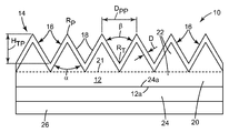
도 1을 참조하면, 예시적인 투명한 반사 방지 구조화된 필름(10)은, 예를 들어, 광에 대해 반사 방지성인 프리즘 모양의 리블렛(16)의 형태로 되어 있는 반사 방지 구조물을 갖는 주 구조화된 면(14)을 가지는 구조화된 필름 기재(12)를 포함하고 있다(도 5 참조). 각각의 반사 방지 구조물(예컨대, 리블렛)(16)은 선단각(tip angle) α, 골과 피크 사이의 높이(trough to peak height) HTP, 및 노출되는 구조화된 표면(18)을 가진다. 2개의 인접한 반사 방지 구조물(예컨대, 리블렛)(16)은 이들 사이의 골각(trough angle) ㅯ 및 피크간 거리(peak to peak distance) DPP를 정의한다. 필름(10)은 기부 부분(20) - 이로부터 반사 방지 구조물(16)이 뻗어 있음 - 을 추가로 포함한다. 기부 부분(20)은, 예시된 바와 같이, 구조물(16)의 일체로 형성된 부분이거나, 파선(21)으로 나타낸 바와 같이 별도의 층일 수 있다. 그의 내구성을 향상시키기 위해, 둥근 피크 RP 및 둥근 골 RT을 갖는 리블렛(16)을 제공하는 것이 바람직할 수 있다.Referring to FIG. 1, an exemplary transparent antireflective
구조화된 필름 기재(12)는 가교 결합된 실리콘 탄성 중합체 물질을 포함한다. 실리콘 탄성중합체 물질은, 예를 들어, 열 경화될 수 있거나 축합 경화될 수 있는 2 부분으로 된(two-part) 실리콘 고무(예컨대, Momentive RTV615 Silicone), 전자빔(e-빔) 경화될 수 있는 폴리다이메틸 실록산(예컨대, 미국 펜실베니아주 모리스빌 소재의 Gelest로부터 입수가능한 DMS-S51) 등, 또는 그 조합일 수 있다. 구조화된 표면을 형성하는 데 사용될 수 있는 실리콘 물질의 기타 특정의 예는 예컨대, Dow Corning으로부터 입수가능한 Sylgard 184, 또는 Wacker Chemie AG로부터 입수가능한 Elastosil 601 등의 다른 하이드로실릴화 경화 실리콘(hydrosilylation cure silicone); 예컨대, Dow Corning으로부터 입수가능한 732 및 734 RTV 실리콘 등의 축합 경화 실리콘; 및 예컨대, Gelest로부터 입수가능한 DMS-S42 또는 Wacker로부터 입수가능한 EL Polymer NA 등의 전자 빔 가교 결합성 실리콘이다.
구조화된 면(14)은 각각의 구조물(16)의 표면(18)의 전부, 대부분 또는 적어도 상당 부분을 정의하는 가교 결합된 실리콘 탄성중합체 물질을 SiO2 화학량론을 포함하는 유리같은 물질로 변환시키는 처리에 노출된다. 실리콘 물질을 VUV(vacuum-ultraviolet, 진공 자외선) 광(예컨대, 172 ㎚ 엑시머 VUV 램프 처리), VUVO(vacuum-ultraviolet light and ozone, 진공 자외선 광 및 오존), 불꽃, 산소 플라즈마, 및 실리콘 탄성중합체 물질 내의 규소 원자를 SiO2 화학량론을 나타내도록 변환시킬 수 있는 임의의 다른 처리 중 하나 또는 그 조합에 노출시키는 것을 포함할 수 있다. 유리같은 물질이 각각의 구조물(16) 내에 깊이 D까지 형성된다. 유리같은 물질의 깊이 D는 처리의 노출 세기 및/또는 지속기간에 의존한다. 이와 같이, 유리같은 물질이 각각의 구조물(16)에 가교 결합된 실리콘 탄성중합체 물질의 코어 또는 나머지(22)를 남기는 또는 전체적으로 유리같은 물질로 형성되어 있는 각각의 구조물(16)을 남기는 깊이 D까지 형성될 수 있다. 나중의 실시 형태에서, [예컨대, 파선(21) 아래에 있는] 필름 기재(12)의 나머지가 미처리된 실리콘 탄성중합체 물질로 이루어져 있을 수 있다. 구조화된 표면(18)을 형성하는 물질이 SiO2 화학량론에 가깝게 나타낼수록, 표면(18)이 오염물 및 먼지 입자 부착에 내성이 있거나(오염물 부착 시험 결과로 표시됨), 내마모성이 있거나(낙사 시험 결과로 표시됨), 또는 둘 다일 가능성이 많다.
이론에 의해 구속받고 싶지 않지만, 유리같은 표면이 고에너지 광자의 흡수를 통해 또는 열 산화를 통해 반사 방지 구조물의 노출된 표면 상의 및 그 근방의 Si-C 결합을 파괴하는 것에 의해 형성되는 것으로 생각되고 있다. 이러한 Si-C 결합의 파괴 후에, SiOH가 생성되고, 이는 응축되어 SiO2 화학량론을 형성한다.While not wishing to be bound by theory, it is believed that glassy surfaces are formed by breaking Si—C bonds on and near the exposed surfaces of antireflective structures through absorption of high energy photons or through thermal oxidation. have. After breaking this Si-C bond, SiOH is produced, which condenses to form SiO 2 stoichiometry.
구조화된 표면(18)의 오염물 및 먼지 입자 부착에 대한 내성(오염물 부착 시험 결과로 표시됨)이 유리같은 표면을 1개 이상의 실리카 나노입자 응집체 층(23)의 코팅으로 코팅하는 것에 의해 추가로 향상될 수 있다. 응집체는 3차원 다공성 실리카 나노입자 네트워크를 포함하며, 실리카 나노입자는 인접한 실리카 나노입자에 결합되어 있다. 실리카 나노입자가 약 5 나노미터(㎚) 내지 최대 약 100 ㎚(이를 포함함)의 범위에 있는 평균 크기(즉, 주 직경 또는 치수)를 가지는 것이 바람직할 수 있다. 실리카 나노입자 코팅이 최대 약 1000 ㎚의 두께를 가지는 것이 바람직할 수 있고, 또한 실리카 나노입자 코팅이 약 20 ㎚ 내지 최대 약 100 ㎚(이를 포함함)의 범위에 있는 두께를 가지는 것이 바람직할 수 있다. 100 ㎚ 초과의 코팅을 도포하는 것은 문제가 될 수 있다. 예를 들어, 이러한 두꺼운 나노입자 코팅으로 인해, 나노입자의 과도한 응집이 일어날 수 있고 및/또는 코팅이 바람직하지 않은 채색 효과를 나타낼 수 있다. 이러한 실리카 나노입자 층은 PCT 공개 제WO2009/140482호, 미국 특허 출원 공개 제US2001/036547호, 및 미국 특허 제3,986,997호 및 제4,027,073호는 물론, PCT 출원 제US2010/056773호, 미국 가특허 출원 제61/390491호(2010년 10월 6일자로 출원됨) 및 제61/262423호(2009년 11월 18일자로 출원됨)(이들 모두는 참조 문헌으로서 그 전체 내용이 본 명세서에 포함됨)에 개시된 것들 중 임의의 하나 또는 그 조합을 포함할 수 있다.Resistance to contaminant and dust particle adhesion of the structured surface 18 (indicated by contaminant adhesion test results) can be further enhanced by coating a glassy surface with a coating of one or more silica nanoparticle aggregate layers 23. Can be. The aggregates comprise a three-dimensional porous silica nanoparticle network, wherein the silica nanoparticles are bound to adjacent silica nanoparticles. It may be desirable for the silica nanoparticles to have an average size (ie, major diameter or dimension) in the range of about 5 nanometers (nm) up to about 100 nm (including). It may be desirable for the silica nanoparticle coating to have a thickness of up to about 1000 nm, and it may also be desirable for the silica nanoparticle coating to have a thickness in the range of about 20 nm to up to about 100 nm (including). . Applying a coating greater than 100 nm can be problematic. For example, due to such thick nanoparticle coatings, excessive aggregation of the nanoparticles can occur and / or the coating can exhibit undesirable coloring effects. Such silica nanoparticle layers include PCT Publication No. WO2009 / 140482, US Patent Application Publication No. US2001 / 036547, and US Patent Nos. 3,986,997 and 4,027,073, as well as PCT Application US2010 / 056773, US Provisional Patent Application. 61/390491 (filed Oct. 6, 2010) and 61/262423 (filed Nov. 18, 2009), all of which are incorporated herein by reference in their entirety. Any one or combinations thereof.
필름(10) 또는 본 발명에 따른 임의의 다른 투명한 반사 방지 구조화된 필름이 선택적인 투명한 지지체 배킹(24)과 결합되어 사용되는 것이 바람직할 수 있다. 이러한 실시 형태에서, 지지체 배킹(24)은 주 면(24a)을 가지며, 구조화된 필름 기재(12)는 투명한 강화된 반사 방지 구조화된 필름을 형성하기 위해 지지체 배킹(24)의 주 면(24a)에 접합되어 있는 주 배킹 면(12a)을 추가로 포함하고 있다. 지지체 배킹(24)은 중합체성 물질 또는 유리 또는 다른 투명한 세라믹 물질을 포함할 수 있다. 예시적인 중합체성 물질은 폴리메틸(메트)아크릴레이트(PMMA) 필름, 폴리비닐리덴 플루오라이드(PVDF) 필름, 폴리에틸렌 테레프탈레이트(PET) 필름, 프라이밍된 PET 필름, 폴리카보네이트 필름, 가교 결합된 폴리우레탄 필름, 아크릴레이트 필름, 에틸렌 테트라플루오로에틸렌(ETFE), 플루오르화된 에틸렌-프로필렌(FEP) 필름, 또는 그 블렌드 중 적어도 하나 또는 그 조합을 포함할 수 있다. 향상된 실외 내구성을 위해 자외광 흡수체[예컨대, Ciba Geigy로부터의 Tinuvin 1577, 및 Sukano TA11-10 MB03 PMMA-UVA 및 Sukano TA07-07 MV02 PET-UVA(둘 다 미국 사우스 캐롤라이나주 덩컨 소재의 Sukano Polymers Corporation으로부터 입수가능함) 등]가 PMMA 및 PVDF와 PMMA의 블렌드에 포함될 수 있다. 다른 투명한 세라믹 물질은, 예컨대, 석영 결정 등일 수 있다. 투명한 부직포 또는 직포 섬유 물질, 또는 절단된 투명한 섬유가 또한 지지체 배킹(24)을 형성하는 데 사용될 수 있다. 이러한 섬유 물질이 구조화된 필름(10) 상에 배치된, 구조화된 필름(10)을 형성하는 실리콘 탄성중합체 물질에 또는 둘 다에 배치될 수 있다.It may be desirable for the
투명한 지지체 배킹(24)이 또한 정전기를 소산시키도록 선택될 수 있다. 예를 들어, 지지체 배킹은 지지체 배킹(24)이 정전기를 소산시킬 수 있게 해주는 하나 이상의 중합체성 물질을 포함할 수 있다. 정전기를 소산시키기 위해, 투명한 지지체 배킹(24)은 또한 Lubrizol Corp.로부터의 STATRITE X5091 폴리우레탄 또는 STATRITE M809 폴리메틸 메타크릴레이트로서 입수가능한 것 등의 본질적으로 정전기 소산 중합체를 포함할 수 있다. 대안적으로, 3M Company로부터 입수가능한 FC4400 등의 정전기 소산염이 투명한 지지체 배킹 24(예컨대, PVDF)를 제조하는 데 사용되는 중합체에 블렌딩될 수 있다. 그에 부가하여 또는 대안적으로, 구조화된 필름 기재(12)는 이러한 정전기 소산염을 포함할 수 있다.The
또한, 필름(10) 또는 본 발명에 따른 임의의 다른 투명한 반사 방지 구조화된 필름이 선택적인 습기 장벽층(moisture barrier layer)(26)과 결합되어 사용되는 것이 바람직할 수 있다. 이러한 실시 형태에서, 예를 들어, 방습 장벽층(26)을 하나 이상의 중간층[예컨대, 지지체 배킹층(24)]을 통해 간접적으로 또는 구조화된 필름 기재(12)의 주 배킹 면(12a) 상에 직접 적층, 코팅 또는 다른 방식으로 접합하는 것에 의해 습기 장벽층(26)이 형성될 수 있다. 대안적으로, 습기 장벽 특성을 나타내도록(예컨대, 흡습, 침윤 등을 억제하기 위해) 필름(10)의 조성물을 조제함으로써 습기 장벽층(26)이 형성될 수 있다.It may also be desirable for the
습기 장벽은, 예를 들어, 장벽 어셈블리 또는 국제 특허 출원 제PCT/US2009/062944호, 미국 특허 제7,486,019호 및 제7,215,473호, 및 미국 특허 출원 공개 제US 2006/0062937 A1호(참조 문헌으로서 그 전체 내용이 본 명세서에 포함됨)에 개시된 장벽층들 중 하나 이상일 수 있다. 습기 장벽이 유용할 수 있는데, 그 이유는 실리콘이 높은 수증기 투과도(moisture vapor transmission rate)를 가지며, 광전지는 전형적으로 습기에 민감하다. 따라서, 습기 장벽층으로 배킹되는 것에 의해, 본 발명의 투명한 반사 방지 구조화된 필름이 습기에 민감한 광전지(예컨대, 구리/인듐/갈륨/셀레늄 또는 CIGS 광전지) 바로 위에 사용될 수 있다.Moisture barriers are described, for example, in barrier assemblies or in International Patent Application Nos. PCT / US2009 / 062944, US Pat. Nos. 7,486,019 and 7,215,473, and US Pat. The contents may be one or more of the barrier layers disclosed herein). Moisture barriers can be useful because silicon has a high moisture vapor transmission rate, and photovoltaic cells are typically sensitive to moisture. Thus, by backing into the moisture barrier layer, the transparent antireflective structured film of the present invention can be used directly on moisture sensitive photovoltaic cells (eg, copper / indium / gallium / selenium or CIGS photovoltaic cells).
도 2를 참조하면, 본 발명의 투명한 반사 방지 구조화된 필름의 다른 실시 형태(10a)에서, 주 구조화된 면(14)이 각각의 반사 방지 구조물(16)의 실리콘 탄성중합체 물질 모두가 SiO2 화학량론을 포함하는 유리같은 물질로 변환되게 하는 정도/지속기간의 처리에 노출된다. 이 실시 형태에서, 필름 기재(12)의 나머지(22)는 실리콘 탄성중합체 물질인 채로 있다. 파선(23)은 기재(12)의 유리같은 물질 부분을 실리콘 탄성중합체 물질 부분과 분리시킨다. 다시 말하지만, 구조화된 표면(18)은 유리같은 표면을 1개 이상의 실리카 나노입자 응집체 층(23)의 코팅으로 코팅하는 것에 의해 추가로 향상될 수 있다Referring to FIG. 2, in another
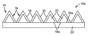
도 3을 참조하면, 본 발명의 투명한 반사 방지 구조화된 필름의 부가의 실시 형태(10b)에서, 각각의 반사 방지 구조물(16)은 별도의 기부 부분(20')으로부터 뻗어 있다. 별도의 기부 부분(20')은 가교 결합된 실리콘 탄성중합체 물질의 하나 이상의 층일 수 있거나, 별도의 기부(20')가 상이한 물질(예컨대, PMMA, PVDF 및 PET와 같은 보다 저렴한 물질)의 하나 이상의 층일 수 있다. 별도의 기부(20')는, 실리콘 탄성중합체 물질과 상이한 물질 사이의 상용성에 따라, 임의의 적당한 수단에 의해 반사 방지 구조물(16)에 접착 또는 다른 방식으로 접합된다. 예를 들어, 기부 부분(20')은 선택적으로 프라이머로 코팅되거나 다른 방식으로 처리(예컨대, 코로나 처리)되거나 각각의 실리콘 탄성중합체 반사 방지 구조물(16)의 주 배킹 면(16a)을 수납하여 그와 접합하도록 준비되는 주 면(20a)을 가질 수 있다. 예를 들어, 반사 방지 구조물(16)의 원하는 패턴과 일치하는 그의 주 표면들 중 적어도 하나에 형성되는 미세-복제된 패턴을 가지는 도구 필름(도시 생략)을 사용함으로써 반사 방지 구조물(16)이 형성될 수 있다.Referring to FIG. 3, in a
원하는 실리콘 탄성중합체 전구체 물질의 층이 기부 부분 면(20a)의 표면 상에 압출, 코팅 또는 다른 방식으로 도포될 수 있다. 도포된 실리콘 탄성중합체 전구체 물질의 노출된 표면을 원하는 반사 방지 구조물(16)의 형상으로 형성하기 위해 도구 필름의 미세-복제된 주 표면이 이어서 실리콘 탄성중합체 전구체 물질의 층과 접촉하게 될 수 있다. 대안적으로, 실리콘 탄성중합체 전구체 물질의 층이 도구 필름의 미세-복제된 주 표면 상에 압출, 코팅 또는 다른 방식으로 도포될 수 있고, 이어서 도포된 전구체 물질의 노출된 후방 표면이 기부 부분 면(20a)의 표면과 접합하도록 적층되거나 다른 방식으로 접촉하게 될 수 있다. 대안적으로, 실리콘 탄성중합체 전구체 물질의 층이 도구 필름의 미세-복제된 주 표면과 기부 부분 면(20a)의 표면 사이에 직접 압출, 코팅 또는 다른 방식으로 도포될 수 있는데, 그 이유는, 예를 들어, 닙 롤 스테이션을 통과하는 등에 의해 3개의 층 모두가 서로 적층되어 있기 때문이다. 형성된 전구체 물질이 기부 부분 면(20a)의 표면과 접촉하면, 실리콘 탄성중합체 전구체 물질이 먼저 가교 결합되거나 경화되고, 도구가 제거되며, 이어서 후속 처리가 행해져 반사 방지 구조물(16)의 적어도 표면(18)에 유리같은 물질을 생성한다.The desired layer of silicone elastomer precursor material may be extruded, coated or otherwise applied onto the surface of the
반사 방지 구조물은 프리즘 모양의, 피라미드형, 원추형, 반구형, 포물선 모양의, 원통형, 및 기둥 모양의 구조물 중 적어도 하나 또는 그 조합을 포함할 수 있다. 프리즘을 포함하는 반사 방지 구조물은 프리즘 선단각 α가 약 90도 미만, 약 60도 이하, 약 30도 이하, 또는 약 10도 내지 최대 약 90도의 범위에 있을 수 있다. 이러한 반사 방지 프리즘 구조물은 또한 골간 또는 피크간 피치 또는 거리가 약 2 마이크로미터 내지 약 2 ㎝의 범위에 있을 수 있다. 프리즘을 포함하는 반사 방지 구조물은 또한 프리즘 선단각이 약 15도 내지 약 75도의 범위에 있을 수 있다. 프리즘을 포함하는 반사 방지 구조물은 또한 골간 또는 피크간 피치가 약 10 마이크로미터 내지 약 250 마이크로미터의 범위에 있을 수 있다. 향상된 내구성을 갖는 반사 방지 구조물(16)의 일 실시 형태에서, 리블렛(16)은 약 5 마이크로미터의 반경을 갖는 둥근 피크 RP 및 골 RT, 약 53도의 골각 β, 약 50 마이크로미터의 피크간 피치 또는 거리 DPP, 및 약 37.7307 마이크로미터의 골과 피크 사이의 높이 HTP를 가진다.The antireflective structure may include at least one or a combination of prismatic, pyramidal, conical, hemispherical, parabolic, cylindrical, and columnar structures. An antireflective structure comprising a prism may have a prism tip angle α of less than about 90 degrees, about 60 degrees or less, about 30 degrees or less, or about 10 degrees up to about 90 degrees. Such antireflective prism structures may also have an interbone or peak to peak pitch or distance in the range of about 2 micrometers to about 2 cm. Antireflective structures comprising prisms can also have a prism tip angle in the range of about 15 degrees to about 75 degrees. Antireflective structures comprising prisms may also have an interbone or interpeak pitch in the range of about 10 micrometers to about 250 micrometers. In one embodiment of the
반사 방지 구조물이 약 1.55 미만인 굴절률, 및 바람직하게는 약 1.50 미만인 굴절률을 나타내는 것이 바람직할 수 있다. 반사 방지 구조물이 프리즘 구조물(즉, 선형 프리즘 구조물 또는 리블렛)을 포함할 때, 각각의 프리즘이 그의 기부로부터 선단 쪽으로 좁아져 정각(apex angle)이 약 90도 미만, 및 바람직하게는 약 60 이하인 것이 바람직할 수 있다. 이러한 프리즘 구조물이 골과 피크 사이의 높이가 약 10 마이크로미터 내지 약 250 마이크로미터의 범위에 있는 것이 바람직할 수 있다. 또한, 이러한 프리즘 구조물이 골과 피크 사이의 높이가 약 25 마이크로미터 내지 약 100 마이크로미터의 범위에 있는 것이 바람직할 수 있다.It may be desirable for the antireflective structure to exhibit a refractive index of less than about 1.55, and preferably a refractive index of less than about 1.50. When the antireflective structure comprises a prism structure (ie, a linear prism structure or riblet), each prism is narrowed from its base toward the tip so that the apex angle is less than about 90 degrees, and preferably about 60 or less. It may be desirable. It may be desirable for such prism structures to have a height between the valleys and the peaks in the range of about 10 micrometers to about 250 micrometers. It may also be desirable for such prismatic structures to have a height between the valleys and the peaks in the range of about 25 micrometers to about 100 micrometers.
구조화된 표면이 오염물 부착 시험, 낙사 시험, 또는 양 시험의 조합에 노출된 후에, 본 발명의 투명한 반사 방지 구조화된 필름이 약 85%, 90%, 91%, 92%, 93%, 94%, 95%, 96%, 97%, 98% 또는 99% 이상의 광 투과율을 나타내는 것이 바람직할 수 있다. 이들 검사에 대해 이하에서 기술한다. 또한, 구조화된 표면이 오염물 부착 시험, 낙사 시험, 또는 양 시험의 조합에 노출된 후에, 본 발명의 투명한 반사 방지 구조화된 필름이 10%, 9%, 8%, 7%, 6%, 5%, 4%, 3%, 2% 또는 1% 미만의 광 투과율 변화를 나타내는 것이 바람직할 수 있다.After the structured surface is exposed to the contaminant adhesion test, the falloff test, or a combination of both tests, the transparent antireflective structured film of the present invention is about 85%, 90%, 91%, 92%, 93%, 94%, It may be desirable to exhibit a light transmittance of at least 95%, 96%, 97%, 98% or 99%. These tests are described below. In addition, after the structured surface is exposed to a contaminant adhesion test, a fallout test, or a combination of both tests, the transparent antireflective structured film of the present invention is 10%, 9%, 8%, 7%, 6%, 5%. It may be desirable to exhibit a light transmittance change of less than 4%, 3%, 2% or 1%.
본 발명의 투명한 반사 방지 구조화된 필름은 또한 반사 방지 구조물의 실리콘 탄성중합체 물질에 무기 입자, 및 바람직하게는 나노입자를 포함할 수 있다. 이들 입자는 임의의 적당한 무기 물질(예컨대, 실리카, 지르코니아, 티타니아, 등 또는 이들의 임의의 조합)을 포함할 수 있다. 이러한 입자는 또한 실란에서의 분산을 촉진시키기 위해 실란 표면 개질로 코팅될 수 있다. 이러한 입자는 크기가 최대 약 2.0 마이크로미터(이를 포함함)의 범위에 있을 수 있다. 실리카 입자는 최대 마이크로미터 크기일 수 있지만, 다른 물질로 이루어진 입자가 나노미터 크기로[즉, 약 5 ㎚ 내지 최대 약 50 ㎚(이를 포함함)의 범위에 있음] 사용되는 것이 바람직하다. 이러한 입자, 특히 나노입자는 또한 0 중량% 내지 최대 약 60 중량%(이를 포함함)의 범위에서 실리콘 탄성 중합체 물질에 로딩될 수 있다.The transparent antireflective structured film of the present invention may also include inorganic particles, and preferably nanoparticles, in the silicone elastomer material of the antireflective structure. These particles may comprise any suitable inorganic material (eg, silica, zirconia, titania, etc. or any combination thereof). Such particles can also be coated with silane surface modification to promote dispersion in silanes. Such particles may range in size up to about 2.0 micrometers (including). The silica particles may be up to micrometers in size, but it is preferred that particles of other materials be used in nanometer sizes (ie, in the range of about 5 nm up to about 50 nm, including). Such particles, in particular nanoparticles, may also be loaded into the silicone elastomer material in the range of 0 wt% to up to about 60 wt%, including.
도 4를 참조하면, 본 발명의 투명한 반사 방지 구조화된 필름(10)의 임의의 실시 형태가, 예를 들어, 광원 열 에너지 흡수 디바이스(예컨대, 태양열 온수 시스템), 광전 디바이스 또는 임의의 다른 광 에너지 흡수 디바이스 등의 광 에너지 흡수 디바이스(30)에 사용될 수 있다. 이러한 디바이스(30)는 또한 광 에너지 수광 면(32a)을 가지는 광 흡수체(32)(예컨대, 광전지)를 포함하고, 투명한 반사 방지 구조화된 필름(10)은 광 에너지 소스(예컨대, 태양)와 광 에너지 수광 면(32a) 사이에 있도록 광 흡수체(32)에 대해 배치되어 있다. 이러한 방식으로, 광원으로부터의 광 에너지는 광 흡수체(32)에 의해 흡수되기 전에 구조화된 필름(10)을 통과한다. 필름(10)은 광 에너지 수광 면(32a)과 직접 접촉하게 접합되거나, 접착되거나, 기계적으로 고정되거나 다른 방식으로 배치될 수 있다. 대안적으로, 원하는 경우, 투명한 지지체 배킹(24) 또는 다른 중간층들 중 하나 이상이 필름(10)과 광 흡수체(32) 사이에 배치될 수 있다.With reference to FIG. 4, any embodiment of the transparent antireflective
도 5를 참조하면, 광 에너지 흡수 디바이스(30)의 광 흡수체(32)를 갖는 본 발명의 투명한 반사 방지 구조화된 필름(10)을 사용함으로써, 반사 방지 구조물(16)의 표면(18)에 충돌하는 입사광(화살표 40으로 나타냄)은 여러번 반사될 가능성이 있다(화살표 40R로 나타냄). 이러한 여러번의 광(40)의 반사는 광(40)이 광 흡수체(32) 내로 굴절될 확률을 증가시키는 것은 물론, 입사광 수광각(acceptance angle)도 증가시킨다. 이러한 방식으로, 이러한 투명한 반사 방지 구조물의 사용은 디바이스(30)의 효율 및 에너지를 증가시킬 수 있다.Referring to FIG. 5, by using the transparent antireflective
광 흡수 디바이스가 광전 디바이스일 때, 광 흡수체는 태양 또는 기타 광 에너지를 전기 에너지로 변환하는 적어도 하나의 광전지를 가지는 광전 모듈이다. 반사 방지 구조화된 필름은 표면 반사를 감소시키고, 이는 광전지에 충돌하는 광의 양을 증가시킬 수 있고, 그 결과 전기 에너지의 생성이 증가된다. 본 발명의 투명한 반사 방지 구조화된 필름을 이러한 방식으로 사용함으로써, 광 에너지를 전기 에너지로 변환하는 효율이 약 3% 이상 및 어쩌면 약 5% 내지 최대 약 10%(이를 포함함)의 범위만큼 향상될 수 있다. 투명한 반사 방지 구조물이 필름의 형태로 되어 있기 때문에, 광전지는 손상되는 일 없이 롤에 감기거나 접히도록 충분히 연성이고 유연할 수 있다.When the light absorbing device is a photovoltaic device, the light absorber is a photovoltaic module having at least one photovoltaic cell that converts the sun or other light energy into electrical energy. Antireflective structured films reduce surface reflections, which can increase the amount of light impinging on photovoltaic cells, resulting in increased production of electrical energy. By using the transparent antireflective structured film of the present invention in this manner, the efficiency of converting light energy into electrical energy can be improved by at least about 3% and possibly in the range of about 5% up to about 10% (including). Can be. Since the transparent antireflective structure is in the form of a film, the photovoltaic cell can be sufficiently soft and flexible to be wound or folded on a roll without being damaged.
본 발명의 광 에너지 흡수 디바이스는, 광이 반사 방지 구조화된 필름을 통해 광 흡수체(예컨대, 광전지)의 광 수광 면 쪽으로 갈 수 있도록, 광 흡수체에 대해 반사 방지 구조화된 필름을 기계적으로 부착하거나, 접착제로 접합시키거나, 다른 방식으로 고정시키는 것에 의해 제조될 수 있다. 광 흡수체는, 예를 들어, 태양열 온수 히터 또는 기타 광 발생 열 에너지 흡수 디바이스, 태양 또는 기타 광 에너지를 전기 에너지로 변환하는 광전지, 또는 그 조합일 수 있다.The light energy absorbing device of the present invention mechanically attaches an antireflective structured film to the light absorber, or an adhesive, so that light can travel through the antireflective structured film toward the light receiving surface of the light absorber (eg, photovoltaic cell). By bonding or by fixing in another way. The light absorber can be, for example, a solar hot water heater or other light generating thermal energy absorbing device, a photovoltaic cell that converts solar or other light energy into electrical energy, or a combination thereof.
본 발명에 따른 투명한 반사 방지 구조화된 필름은 앞서 기술한 바와 같이 투명한 구조화된 필름 기재를 제공하고 이어서, 구조화된 표면을 정의하는 가교 결합된 실리콘 탄성중합체 물질의 전부, 대부분 또는 적어도 상당 부분이 SiO2 화학량론을 포함하는 유리같은 물질로 변환되도록, 구조화된 표면을 처리하는 것에 의해 제조될 수 있다. 이 유리같은 표면은 이어서 적어도 하나의 실리카 나노입자 응집체 층을 포함하는, 본질적으로 그 층으로 이루어져 있는, 또는 그 층으로 이루어져 있는 코팅으로 코팅되고, 응집체는 3차원 다공성 실리카 나노입자 네트워크를 포함하고, 실리카 나노입자는 인접한 실리카 나노입자에 결합되어 있다.The transparent antireflective structured film according to the present invention provides a transparent structured film substrate as described above, and then all, most or at least a substantial portion of the crosslinked silicone elastomer material defining the structured surface is SiO 2. It can be prepared by treating a structured surface to be converted into a glassy material including stoichiometry. This glassy surface is then coated with a coating consisting essentially of, or consisting of, a layer comprising at least one silica nanoparticle aggregate layer, the aggregate comprising a three-dimensional porous silica nanoparticle network, Silica nanoparticles are bound to adjacent silica nanoparticles.
초기의 구조화된 필름 기재의 반사 방지 구조화된 표면은, 예를 들어, 반사 방지 구조화된 표면을, 예를 들어, VUV(vacuum-ultraviolet) 광(예컨대, 172 ㎚ 엑시머 처리에 의함), VUVO(vacuum-ultraviolet light and ozone), 산소 플라즈마, 및 열(예컨대, 유도 가열, 불꽃 등) 중 적어도 하나 또는 그 조합 등의 임의의 적당한 처리에 노출시키는 것에 의해, 유리같은 표면을 형성하도록 처리될 수 있다. 대량 제조 설정에서 사용하기에 적합하도록 하기 위해, 이러한 처리가 비교적 신속하게 수행될 필요가 있다. 상세하게는, 예를 들어, 고속(즉, 대량) 웨브-기반 제조 공정은, 예를 들어, 약 5분 이하 정도로 짧은 처리 시간을 사용할 필요가 있을 것이다. 이와 동시에, 규소로부터 SiO2 화학량론으로의 원하는 레벨의 변환을 생성하기 위해, 실리콘 물질의 표면은 충분한 기간(예컨대, 5 내지 300 초의 172 ㎚ 엑시머 램프 노출) 동안 적당한 에너지 레벨(예컨대, 50 ppm 미만의 산소를 갖는 질소 불활성 분위기에서 10 내지 50 mW/㎠)에서 처리될 필요가 있다. 유리같은 표면을 생성하기 위해 사용되는 처리의 설정(예컨대, 세기 및/또는 지속기간)에 따라, 유리같은 물질로 변환되지 않은 구조화된 필름 기재의 남아 있는 부분이 있을 수 있다. 예를 들어, 도 2에서 보는 바와 같이, 처리 설정이 또한 각각의 반사 방지 구조물을 정의하는 가교 결합된 실리콘 탄성중합체 물질 전부가 SiO2 화학량론을 포함하는 유리같은 물질로 변환되도록 선택될 수 있다. 대안적으로, 처리 설정이 각각의 반사 방지 구조물의 코어 부분이 실리콘 탄성중합체 물질인 채로 있도록 선택될 수 있다(도 1, 도 3 및 도 4 참조). 에너지 비용을 절감하기 위해, 반사 방지 구조화된 표면이 유리같은 표면으로 변환되는 깊이 및 정도를 최소화하는 것이 바람직할 수 있다.The antireflective structured surface of the initial structured film substrate may, for example, form an antireflective structured surface, eg, by vacuum-ultraviolet (VUV) light (eg, by 172 nm excimer treatment), VUVO (vacuum). -ultraviolet light and ozone), oxygen plasma, and heat (eg, induction heating, flames, etc.) by exposure to any suitable treatment, such as at least one or a combination thereof, can be processed to form a glassy surface. In order to be suitable for use in high volume manufacturing settings, this process needs to be performed relatively quickly. Specifically, for example, high speed (ie, large volume) web-based manufacturing processes will need to use treatment times as short as, for example, about 5 minutes or less. At the same time, in order to produce the desired level of conversion from silicon to SiO 2 stoichiometry, the surface of the silicon material must be at an appropriate energy level (eg less than 50 ppm) for a sufficient period of time (eg, 172 nm excimer lamp exposure of 5 to 300 seconds). In an inert atmosphere of nitrogen with oxygen of 10 to 50 mW / cm 2). Depending on the set of treatments (eg, intensity and / or duration) used to create the glassy surface, there may be remaining portions of the structured film substrate that are not converted to glassy materials. For example, as shown in FIG. 2, the treatment setup may also be selected such that all of the crosslinked silicone elastomer material defining each antireflective structure is converted to a glassy material including SiO 2 stoichiometry. Alternatively, the treatment setup may be selected such that the core portion of each antireflective structure remains a silicone elastomer material (see FIGS. 1, 3, and 4). To save energy costs, it may be desirable to minimize the depth and extent to which the antireflective structured surface is converted to a glassy surface.
투명한 구조화된 필름 기재는 가교 결합된 실리콘 전구체 물질을 형성하기 위해 경화가능한 실리콘 탄성중합체 전구체 물질을 제공하는 것에 의해 제조될 수 있다. 이 실리콘 탄성중합체 전구체 물질은 임의의 적당한 형성 기법을 사용하여 구조화된 필름 기재의 형상으로 형성된다. 예를 들어, 적절한 크기의 홈이 기재에 형성될 수 있고, 이어서 구조화된 필름 기재의 반사 방지 구조물을 갖는 주 구조화된 면을 주조하기 위해 기재가 실리콘 탄성중합체 전구체 물질이 코팅되는 몰드 표면으로서 사용될 수 있다. 이러한 몰드 표면은, 예를 들어, 미국 특허 공개 제US 2006/0234605호(참조 문헌으로서 그 전체 내용이 본 명세서에 포함됨)에 개시된 기법 및 장비에 따라 제조될 수 있다. 이 형상으로 있는 동안, 실리콘 탄성중합체 전구체 물질이 경화되어 구조화된 필름 기재를 형성한다. 대안적으로, 미국 특허 공개 제US 2006/0234605호에 개시된 도구는 나중에 몰드 표면으로서 사용되는 중합체 몰드 기재(예컨대, 필름 형태로 되어 있음)에 적절한 크기의 홈을 주조하는 데 사용될 수 있다. 사용되는 실리콘 탄성중합체 전구체 물질에 따라, 경화 공정은 전구체 물질을 가교 결합 처리(예컨대, 열 및/또는 방사 처리)를 거치게 하는 것을 포함할 수 있다. 전구체 물질이 2 부분으로 된 자기 경화 실리콘 탄성중합체 물질일 때, 경화 공정은 2 부분이 혼합된 후 가교 결합이 일어날 수 있기에 충분한 기간 동안 전구체 물질을 몰드 표면과 접촉한 채로 유지하는 것을 포함할 수 있다.Transparent structured film substrates can be made by providing a curable silicone elastomer precursor material to form a crosslinked silicone precursor material. This silicone elastomer precursor material is formed into the shape of the structured film substrate using any suitable forming technique. For example, an appropriately sized groove can be formed in the substrate and then the substrate can be used as a mold surface to which the silicone elastomer precursor material is coated to cast the main structured side with the antireflective structure of the structured film substrate. have. Such mold surfaces may be prepared according to the techniques and equipment disclosed, for example, in US 2006/0234605, incorporated herein by reference in its entirety. While in this shape, the silicone elastomer precursor material cures to form a structured film substrate. Alternatively, the tool disclosed in US 2006/0234605 may be used to cast grooves of a suitable size to a polymer mold substrate (eg, in the form of a film) that is later used as mold surface. Depending on the silicone elastomer precursor material used, the curing process may include subjecting the precursor material to a crosslinking treatment (eg, heat and / or spinning treatment). When the precursor material is a two part self-curing silicone elastomer material, the curing process may include keeping the precursor material in contact with the mold surface for a period of time sufficient to allow crosslinking to occur after the two parts are mixed. .
유리같은 표면을 적어도 하나의 실리카 나노입자 응집체 층으로 코팅하는 단계는, 예를 들어, 앞서 포함된 PCT 공개 제WO2009/140482호, 미국 특허 출원 공개 제US2001/036547호, 및 미국 특허 제3,986,997호 및 제4,027,073호는 물론, PCT 출원 제US2010/056773호, 미국 가특허 출원 제61/390491호(2010년 10월 6일자로 출원됨) 및 제61/262423호(2009년 11월 18일자로 출원됨)에 개시된 기법에 따라 수행될 수 있다. 실리카 나노입자 코팅의 양호한 젖음을 달성하기 위해, 유리같은 표면이 친수성 특성을 나타내는 것이 바람직할 수 있다. 또한, 나노입자를 서로 소결하도록 유도하기 위해 (예컨대, 불꽃, 유도 가열 등에 의해) 실리카 나노입자 코팅에 열을 가하는 것이 바람직할 수 있다. 이러한 소결 단계를 제한하는 것이 바람직할 수 있고, 그렇지 않으면, 실리카 나노입자 응집체의 과도한 평탄화가 일어날 수 있다. 하나 이상의 실리카 나노입자 응집체 층을 도포하기 위해 다양한 코팅 기법이 사용될 수 있지만, 이러한 코팅을 도포하기 위해 종래의 에어 나이프 코팅(air-knife coating) 기법을 사용하는 것이 바람직하다는 것을 알았다. 이러한 에어 나이프 코팅 공정은 유리같은 반사 방지 구조화된 표면 상에의 실리카 나노입자 응집체의 비교적 얇은 코팅을 보장해주는 데 도움을 준다.Coating a glassy surface with at least one layer of silica nanoparticle aggregates is described, for example, in PCT Publication No. WO2009 / 140482, US Patent Application No. US2001 / 036547, and US Patent Nos. 3,986,997 and 4,027,073, as well as PCT Application US2010 / 056773, US Provisional Patent Application 61/390491 (filed October 6, 2010) and 61/262423 (filed November 18, 2009) It can be carried out according to the technique disclosed in). In order to achieve good wetting of the silica nanoparticle coating, it may be desirable for the glassy surface to exhibit hydrophilic properties. It may also be desirable to heat the silica nanoparticle coating (eg, by flame, induction heating, etc.) to induce the nanoparticles to sinter each other. It may be desirable to limit this sintering step, otherwise excessive planarization of the silica nanoparticle aggregates may occur. Although various coating techniques can be used to apply one or more layers of silica nanoparticle aggregates, it has been found that it is desirable to use conventional air-knife coating techniques to apply such coatings. This air knife coating process helps to ensure a relatively thin coating of the silica nanoparticle aggregates on the antireflective structured surface, such as glass.
하기의 실시예들은 단지 본 발명의 특징, 장점 및/또는 기타 상세 사항을 추가로 설명하기 위하여 선택되었다. 그러나, 이 실시예들이 이와 같은 목적을 갖지만, 사용된 특정 성분과 양 및 기타 조건과 상세 사항은 본 발명의 범주를 부당하게 제한하는 방식으로 해석되지 않아야 한다는 것을 명확히 이해하여야 한다.The following examples are only chosen to further illustrate the features, advantages and / or other details of the invention. It is to be expressly understood, however, that these embodiments have this purpose, but that the particular components and amounts used and other conditions and details should not be construed in a manner that would unduly limit the scope of the invention.
실시예Example
실시예 1Example 1
RTV615 Part A 및 RTV615 Part B(미국 뉴욕주 워터포트 소재의 Momentive Performance Materials로부터 입수가능함)가 10:1 비율로 혼합되고 100 마이크로미터 두께로 4개의 석영 유리 슬라이드 각각에 코팅되었다. 이어서, 열 경화성 실리콘 탄성중합체 전구체 물질을 가교 결합/경화시키기 위해 실리콘 코팅된 석영 유리 슬라이드가 컨벡션 오븐에서 30분 동안 85℃로 가열되었다. 가교 결합된 실리콘으로 코팅된 이들 유리 슬라이드(샘플 2 내지 샘플 5)는 이어서 표 1에 나타낸 바와 같이 화염 처리에 노출되었다. 저장 탄성률을 알아보기 위해, 이들 화염 처리된 실리콘 코팅된 유리 구조체는 이어서 나노 압입에 의해 분석되었다. 이들 화염 처리된 실리콘 코팅된 유리 구조체에서의 탄성률 변화가 표 1에 나타내어져 있다.RTV615 Part A and RTV615 Part B (available from Momentive Performance Materials, Waterport, NY) were mixed in a 10: 1 ratio and coated on each of four quartz glass slides at 100 micrometer thickness. The silicone coated quartz glass slide was then heated to 85 ° C. for 30 minutes in a convection oven to crosslink / cure the heat curable silicone elastomer precursor material. These glass slides (Samples 2-5) coated with crosslinked silicone were then exposed to flame treatment as shown in Table 1. To determine the storage modulus, these flame treated silicon coated glass structures were then analyzed by nanoindentation. The modulus change in these flame treated silicone coated glass structures is shown in Table 1.
[표 1][Table 1]

실시예 2Example 2
14개의 7.6 cm(3 인치) × 5.1 ㎝(2 인치) 유리 슬라이드(VWR International, LLC.로부터 입수가능함)가 나노-실리카 기반 프라이머로 프라이밍되었다. 나노-실리카 프라이머는 H2O 중에서 70:30 비의 제1 콜로이드성 실리카("NALCO 1115 COLLOIDAL SILICA")와 제2 콜로이드성 실리카("NALCO 1050 colloidal SILICA")의 5 중량% 블렌드(HNO3에 의해 2.5 내지 2.0의 pH로 됨)로 이루어져 있다. 나노-실리카 프라이머 용액으로 적셔져 있는 작은 와이프(미국 조지아주 로스웰 소재의 Kimberly-Clark으로부터 "KIMTECH"라는 상표명으로 입수됨)로 표면을 와이핑함으로써, 프라이머의 얇은(약 100 나노미터) 균일한 코팅이 각각의 유리 슬라이드에 도포되었다. 프라이머가 실온에서 건조될 수 있었다. 부가 경화 실리콘(미국 미시간주 미들랜드 소재의 Dow Corning으로부터 입수가능한 Sylgard 184)이 10:1(부분 A 대 부분 B)의 비율로 혼합되었고, 프라이밍된 유리 슬라이드의 표면에 45 마이크로미터의 두께로 매끄러운 코팅으로 도포되어 48 시간 동안 완전히 경화될 수 있었다. 샘플 6 및 샘플 7에서는, 실리콘의 표면이 처리되지 않은 반면, 샘플 8 내지 샘플 19는 68.6-㎝(27-인치) 하부 전력 공급 전극 및 중앙 가스 펌핑과 함께 반응성 이온 에칭(RIE)을 하도록 구성되어 있는 상용 배치 플라즈마 시스템(batch plasma system)(Plasmatherm Model 3032)을 사용하여 산소 플라즈마 처리되었다. 챔버를 건식 기계식 펌프(에드워즈 모델 iQDP80)에 의해 지원되는 루츠 블로어(roots blower)(에드워즈 모델 EH1200)에 의해 펌핑한다. RF 전력이 임피던스 정합 회로망을 통해 3 kW, 13.56 Mhz 고상 발전기(solid-state generator)(RFPP Model RF30H)에 의해 전달된다. 시스템은 공칭 기저 압력이 0.67 Pa(5 mTorr)이다. 가스의 유량을 MKS 유동 제어기에 의해 제어하였다. 플라즈마 처리를 위한 기재가 하부 전력 공급 전극 상에 위치된다. 실리콘 코팅된 유리 슬라이드가 배치 플라즈마 장치의 전력 공급 전극 상에 위치되었다. 90초 동안 산소 가스(Oxygen Service Corporation, UHP Grade)를 500 sccm(standard cm3/min)의 흐름 속도 및 3000 와트의 플라즈마 전력으로 유동시킴으로써 산소 플라즈마에 의해 플라즈마 처리가 수행되었다. 플라즈마 처리가 완료된 후에, 챔버가 대기로 배기되고 샘플이 제거되었다.Fourteen 7.6 cm (3 inch) x 5.1 cm (2 inch) glass slides (available from VWR International, LLC.) Were primed with nano-silica based primers. The nano-silica primer was prepared in a 5% by weight blend (HNO 3 ) of a first colloidal silica ("NALCO 1115 COLLOIDAL SILICA") and a second colloidal silica ("NALCO 1050 colloidal SILICA") in a 70:30 ratio in H 2 O. By a pH of 2.5 to 2.0). Thin (approximately 100 nanometers) uniform coating of the primer by wiping the surface with a small wipe (obtained under the trade name "KIMTECH" from Kimberly-Clark, Roswell, GA, US) wetted with nano-silica primer solution. This was applied to each glass slide. The primer could be dried at room temperature. Additive cured silicone (Sylgard 184, available from Dow Corning, Midland, Mich.) Was mixed at a ratio of 10: 1 (Part A to Part B) and a smooth coating of 45 micrometers thick on the surface of the primed glass slide It could be applied and cured completely for 48 hours. In Samples 6 and 7, the surface of the silicon was untreated, while Samples 8-19 were configured to perform reactive ion etching (RIE) with a 68.6-cm (27-inch) bottom power supply electrode and central gas pumping. Oxygen plasma treatment was performed using a commercial batch plasma system (Plasmatherm Model 3032). The chamber is pumped by a roots blower (Edwards model EH1200) supported by a dry mechanical pump (Edwards model iQDP80). RF power is delivered by a 3 kW, 13.56 Mhz solid-state generator (RFPP Model RF30H) through an impedance matching network. The system has a nominal base pressure of 0.6 m Pa (5 mTorr). The flow rate of the gas was controlled by the MKS flow controller. A substrate for the plasma treatment is located on the lower power supply electrode. A silicon coated glass slide was placed on the power supply electrode of the batch plasma apparatus. Plasma treatment was performed by oxygen plasma by flowing oxygen gas (Oxygen Service Corporation, UHP Grade) at a flow rate of 500 sccm (standard cm 3 / min) and a plasma power of 3000 watts for 90 seconds. After the plasma treatment was completed, the chamber was evacuated to atmosphere and samples removed.
샘플 6 내지 샘플 17은, 하나의 코팅되지 않은 보통의 유리 슬라이드와 함께, 이하에서 기술하는 오염물 부착 시험 #1을 주기적으로 거쳤으며, 시험되기 이전의 초기 광 투과율(Ti), 시험된 후의 최종 광 투과율(Tf), 및 초기 광 투과율과 최종 광 투과율 간의 차이(Td) 각각이 이하의 표 2(오염물 부착 시험 #1 결과)에 표로 나타내어져 있다. 탁도계를 사용하여 투과율이 시험되었다. 표로 나타낸 데이터는, 미처리된 샘플 6 및 샘플 7에 비해, 산소 플라즈마 처리된 샘플 8 내지 샘플 17의 광 투과율의 상당한 증가를 보여주고 있다. 이러한 광 투과율 차이는 부가적으로 처리된 실리콘 탄성중합체 표면(샘플 8 내지 샘플 17)이 미처리된 샘플 6 및 샘플 7보다 적은 오염물을 부착하고 보유하는 것에 의해 야기된다. 표 2 데이터는 또한 처리된 샘플 6 내지 샘플 17이 보통의 유리 슬라이드의 광 투명도와 비슷한 광 투명도를 나타내었음을 보여주고 있다.Samples 6-17, with one uncoated normal glass slide, were periodically subjected to Contaminant Adhesion Test # 1, described below, with initial light transmittance (Ti) before testing, and final light after testing. The transmittance Tf and the difference Td between the initial light transmittance and the final light transmittance, respectively, are shown in a table in the following Table 2 (contaminant adhesion test # 1 result). Permeability was tested using a turbidimeter. The tabulated data shows a significant increase in light transmittance of samples 8 to 17 treated with oxygen plasma compared to untreated samples 6 and 7. This light transmittance difference is caused by the additionally treated silicone elastomer surface (Samples 8-17) attaching and retaining less contaminants than untreated Samples 6 and 7. Table 2 data also shows that treated Samples 6-17 exhibited light transparency similar to that of ordinary glass slides.
[표 2][Table 2]

샘플 18 및 샘플 19는 이하에서 기술하는 낙사 시험을 거쳤으며, 시험되기 이전의 초기 광 투과율(Ti), 시험된 후의 최종 광 투과율(Tf), 및 초기 광 투과율과 최종 광 투과율 간의 차이(Td)가 이하의 표 3(낙사 시험)에 표로 나타내어져 있다. 표로 나타낸 데이터는 처리된 샘플 18 및 샘플 19가 보통의 유리 슬라이드의 광 투명도와 비슷한 광 투명도를 나타내었음을 보여주고 있다.
[표 3][Table 3]

샘플 18 및 샘플 19는 또한 낙사 시험 직후에 오염물 시험을 거쳤으며, 낙사 시험 후의 투과율 값을 나타내는 초기 투과율(Ti), 오염물 시험 후의 투과율 값을 나타내는 최종 투과율(Tf), 및 초기 투과율과 최종 투과율 간의 차이(Td)는 이하의 표 4(낙사 시험 직후의 오염물 시험 #1 결과)에 표로 나타내어져 있다. 표로 나타낸 데이터는 산소 플라즈마 처리된 실리콘 샘플이 보통의 유리 슬라이드의 성능으로부터 2% 내에 있다는 것을 보여주고 있다.
[표 4][Table 4]

실시예Example 3 3
2개의 30.5 ㎝(12 인치) × 15.2 ㎝(6 인치) 폴리에틸렌 테레프탈레이트(PET)(미국 버지니아주 체스터 소재의 DuPont Teijin Films으로부터 "Melinex 618"이라는 상표명으로 획득됨) 시트가 나노-실리카 기반 프라이머로 프라이밍되었다. 나노-실리카 프라이머는 H2O 중에서 70:30 비의 제1 콜로이드성 실리카("NALCO 1115 COLLOIDAL SILICA")와 제2 콜로이드성 실리카("NALCO 1050 colloidal SILICA")의 5 중량% 블렌드(HNO3에 의해 2.5 내지 2.0의 pH로 됨)로 이루어져 있다. 나노-실리카 프라이머 용액으로 적셔져 있는 작은 와이프(미국 조지아주 로스웰 소재의 Kimberly-Clark으로부터 "KIMTECH"라는 상표명으로 입수됨)로 표면을 와이핑함으로써, 프라이머의 얇은(약 100 나노미터) 균일한 코팅이 각각의 유리 슬라이드에 도포되었다. 프라이머가 실온에서 건조될 수 있었다. 실라놀 말단 폴리다이메틸실록산 유체(미국 펜실베니아주 모리스빌 소재의 Gelest Inc.로부터 입수가능한 DMS-S51)가 노치 바 코터(notch bar coater)를 사용하여 프라이밍된 PET 필름 상에 100 마이크로미터의 두께로 코팅되었다. 실리콘 코팅을 갖는 PET 필름이 캐리어 웨브에 테이핑되고, 190 keV의 가속 전압 및 10 MRad의 선량의 전자 빔을 통과하였다. E-빔 유닛은 광대역 커튼형 전자 빔 처리기(PCT Engineered Systems, LLC로부터 입수됨)였다. 6개의 편부(샘플 20, 샘플 21, 샘플 22, 샘플 23, 샘플 24 및 샘플 25)가 하나의 실리콘 코팅된 필름으로부터 절단되었고, 샘플 20, 샘플 21, 샘플 22 및 샘플 23은 실리콘 코팅의 표면이 질소 퍼징(nitrogen purging)과 함께 10 mW/㎠의 방사 조도(irradiance)로 120초 동안 172 ㎚ 엑시머 램프(미국 캘리포니아주 사이프러스 소재의 Ushio America, Inc.로부터 입수가능한 Model UER20-172)에 노출되었다. 샘플 24 및 샘플 25는 엑시머 램프 처리를 받지 않았다. 6개의 편부(샘플 26, 샘플 27, 샘플 28, 샘플 29, 샘플 30 및 샘플 31)가 표면을 추가로 가교 결합시키기 위해 120 keV에서 15 MRad/패스(pass)의 선량으로 4번의 패스의 추가의 e-빔 선량을 받은 다른 실리콘 코팅된 필름으로부터 절단되었다. 샘플 26, 샘플 27, 샘플 28 및 샘플 29는 이어서 10 mW/㎠의 방사 조도에서 172 ㎚ 엑시머 램프에 120초 동안 노출되었다. 샘플 30 및 샘플 31은 엑시머 램프 처리를 받지 않았다.Two 30.5 cm (12 inch) by 15.2 cm (6 inch) polyethylene terephthalate (PET) (obtained under the trade name "Melinex 618" from DuPont Teijin Films, Chester, VA) as a nano-silica based primer Primed. The nano-silica primer was prepared in a 5% by weight blend (HNO 3 ) of a first colloidal silica ("NALCO 1115 COLLOIDAL SILICA") and a second colloidal silica ("NALCO 1050 colloidal SILICA") in a 70:30 ratio in H 2 O. By a pH of 2.5 to 2.0). Thin (approximately 100 nanometers) uniform coating of the primer by wiping the surface with a small wipe (obtained under the trade name "KIMTECH" from Kimberly-Clark, Roswell, GA, US) wetted with nano-silica primer solution. This was applied to each glass slide. The primer could be dried at room temperature. The silanol terminated polydimethylsiloxane fluid (DMS-S51, available from Gelest Inc., Morrisville, Pa.) Was 100 micrometers thick on a PET film primed using a notch bar coater. Coated. The PET film with the silicone coating was taped to the carrier web and passed through an electron beam of an acceleration voltage of 190 keV and a dose of 10 MRad. The E-beam unit was a broadband curtain electron beam processor (obtained from PCT Engineered Systems, LLC). Six portions (
샘플 20, 샘플 21, 샘플 24, 샘플 26, 샘플 27 및 샘플 30은 이하에서 기술하는 오염물 부착 시험 #1을 거쳤으며, 시험되기 이전의 초기 광 투과율(Ti), 시험된 후의 최종 광 투과율(Tf), 및 초기 광 투과율과 최종 광 투과율 간의 차이(Td) 각각이 이하의 표 5(오염물 부착 시험 #1 결과)에 표로 나타내어져 있다. 표로 나타낸 데이터는, 미처리된 샘플 24 및 샘플 30에 비해, 부가적으로 처리된 샘플 20, 샘플 21, 샘플 26 및 샘플 27의 광 투과율의 상당한 증가를 보여주고 있다. 이러한 광 투과율 차이는 부가적으로 처리된 실리콘 탄성중합체 표면(샘플 20, 샘플 21, 샘플 26 및 샘플 27)이 미처리된 샘플 24 및 샘플 30보다 적은 오염물을 부착하고 보유하는 것에 의해 야기된다. 표 5 데이터는 또한 처리된 샘플 20, 샘플 21, 샘플 26 및 샘플 27이 표 5로부터의 보통의 유리 슬라이드의 광 투명도와 비슷한 광 투명도를 나타내었음을 보여주고 있다. 이 표는 또한 샘플 30에서의 추가의 전자 빔 가교 결합으로 인해, 172 ㎚ 엑시머 램프 처리가 없더라도, 전자빔도 172 ㎚ 엑시머 램프 처리도 받지 않은 샘플 24에 비해 투과율이 덜 상실된다는 것을 보여주고 있다.
[표 5][Table 5]

샘플 22, 샘플 23, 샘플 25, 샘플 28, 샘플 29 및 샘플 31은 이하에서 기술하는 낙사 시험을 거쳤으며, 시험되기 이전의 초기 광 투과율(Ti), 시험된 후의 최종 광 투과율(Tf), 및 초기 광 투과율과 최종 광 투과율 간의 차이(Td)가 이하의 표 6(낙사 시험)에 표로 나타내어져 있다. 표로 나타낸 데이터는, 부가적으로 전자빔 가교 결합되지 않은 샘플 22 및 샘플 23에 비해, 172 ㎚ 엑시머 램프 처리 이전에 부가적으로 전자 빔 가교 결합된 샘플 28 및 샘플 29의 광 투과율의 증가(즉, 낙사 시험 결과)를 보여주고 있다. 이 표는 또한 샘플 31에서의 172 ㎚ 엑시머 램프 처리 없는 추가의 전자 빔 가교 결합으로 인해 추가의 전자 빔 가교 결합도 172 ㎚ 엑시머 레이저 처리를 받지 않은 샘플 25는 물론, 172 ㎚ 엑시머 램프 처리만을 받은 샘플 22 및 샘플 23 그리고 추가의 전자 빔 가교 결합 및 172 ㎚ 엑시머 램프 처리 둘 다를 받은 샘플 28 및 샘플 29에 비해 투과율이 덜 상실된다는 것을 보여주고 있다.
[표 6][Table 6]

실시예 4Example 4
2개의 30.5 ㎝(12 인치) × 15.2 ㎝(6 인치) 폴리에틸렌 테레프탈레이트(PET)(미국 버지니아주 체스터 소재의 DuPont Teijin Films으로부터 "Melinex 618"이라는 상표명으로 획득됨) 시트가 나노-실리카 기반 프라이머로 프라이밍되었다. 나노-실리카 프라이머는 H2O 중에서 70:30 비의 제1 콜로이드성 실리카("NALCO 1115 COLLOIDAL SILICA")와 제2 콜로이드성 실리카("NALCO 1050 colloidal SILICA")의 5 중량% 블렌드(HNO3에 의해 2.5 내지 2.0의 pH로 됨)로 이루어져 있다. 나노-실리카 프라이머 용액으로 적셔져 있는 작은 와이프(미국 조지아주 로스웰 소재의 Kimberly-Clark으로부터 "KIMTECH"라는 상표명으로 입수됨)로 표면을 와이핑함으로써, 프라이머의 얇은(약 100 나노미터) 균일한 코팅이 각각의 유리 슬라이드에 도포되었다. 프라이머가 실온에서 건조될 수 있었다. 열 경화 실리콘 탄성중합체(미국 미시간주 미들랜드 소재의 Dow Corning으로부터 입수가능한 Sylgard 184)가 프라이밍된 PET와 반사 방지 표면 구조물을 포함하는 폴리프로필렌 도구 필름 사이에 코팅되었다. 실리콘 코팅을 경화시키기 위해, 실리콘 코팅 및 폴리프로필렌 도구 필름을 갖는 PET 필름이 75℃에서 90분 동안 오븐에 위치되었다. 오븐으로부터 필름을 제거한 후에, 도구 필름이 제거되었고, 그 결과 표면 구조화된 반사 방지 실리콘 코팅이 PET 필름에 부착되었다. 실리콘 표면 구조물의 표면에서의 내구성의 향상을 위한 추가의 가교 결합을 제공하기 위해, 한장의 코팅된 필름이 이어서 캐리어 웨브에 테이핑되었고, 4번의 패스에 대해 120 keV의 가속 전압 및 15 MRad/패스로 전자 빔을 통과하였다. E-빔 유닛은 광대역 커튼형 전자 빔 처리기(PCT Engineered Systems, LLC로부터 입수됨)였다.Two 30.5 cm (12 inch) by 15.2 cm (6 inch) polyethylene terephthalate (PET) (obtained under the trade name "Melinex 618" from DuPont Teijin Films, Chester, VA) as a nano-silica based primer Primed. The nano-silica primer was prepared in a 5% by weight blend (HNO 3 ) of a first colloidal silica ("NALCO 1115 COLLOIDAL SILICA") and a second colloidal silica ("NALCO 1050 colloidal SILICA") in a 70:30 ratio in H 2 O. By a pH of 2.5 to 2.0). Thin (approximately 100 nanometers) uniform coating of the primer by wiping the surface with a small wipe (obtained under the trade name "KIMTECH" from Kimberly-Clark, Roswell, GA, US) wetted with nano-silica primer solution. This was applied to each glass slide. The primer could be dried at room temperature. A thermoset silicone elastomer (Sylgard 184, available from Dow Corning, Midland, Mich.) Was coated between the primed PET and a polypropylene tool film comprising an antireflective surface structure. To cure the silicone coating, a PET film with a silicone coating and a polypropylene tool film was placed in an oven at 75 ° C. for 90 minutes. After removing the film from the oven, the tool film was removed, resulting in a surface structured antireflective silicone coating attached to the PET film. To provide additional crosslinking for improved durability at the surface of the silicon surface structure, one coated film was then taped to the carrier web, with an acceleration voltage of 120 keV and 15 MRad / pass for four passes. Passed through the electron beam. The E-beam unit was a broadband curtain electron beam processor (obtained from PCT Engineered Systems, LLC).
4개의 편부(샘플 32, 샘플 33, 샘플 34, 및 샘플 35)가 추가의 전자 빔 처리를 받지 않은 실리콘 코팅된 필름으로부터 절단되었고, 샘플 32 및 샘플 33은 질소 퍼징과 함께 대략 10 mW/㎠의 방사 조도로 172 ㎚ 엑시머 램프(Ushio Model UER20-172)에 300초 동안 노출된 실리콘 코팅의 표면을 가졌다. 샘플 34 및 샘플 35는 엑시머 램프 처리를 받지 않았다. 4개의 편부(샘플 36, 샘플 37, 샘플 38, 및 샘플 39)가 추가의 e-빔 처리를 받은 다른 실리콘 코팅된 필름으로부터 절단되었다. 샘플 37 및 샘플 37은 이어서 대략 10 mW/㎠의 방사 조도에서 172 ㎚ 엑시머 램프에 300초 동안 노출되었다. 샘플 38 및 샘플 39는 엑시머 램프 처리를 받지 않았다.Four portions (
샘플 32, 샘플 34, 샘플 36 및 샘플 38은 이하에서 기술하는 오염물 부착 시험 #1을 거쳤으며, 시험되기 이전의 초기 광 투과율(Ti), 시험된 후의 최종 광 투과율(Tf), 및 초기 광 투과율과 최종 광 투과율 간의 차이(Td) 각각이 이하의 표 7(오염물 부착 시험 #1 결과)에 표로 나타내어져 있다. 표로 나타낸 데이터는, 미처리된 샘플 34 및 샘플 38에 비해, 172 ㎚ 엑시머 램프 처리된 샘플 32 및 샘플 36의 광 투과율의 상당한 증가를 보여주고 있다. 이러한 광 투과율 차이는 172 ㎚ 엑시머 램프 처리된 실리콘 탄성중합체 표면(샘플 32 및 샘플 36)이 미처리된 샘플 34 및 샘플 38보다 적은 오염물을 부착하고 보유하는 것에 의해 야기된다. 표 7 데이터는 또한 172 ㎚ 엑시머 램프 처리 이전에 부가적인 전자 빔 가교 결합을 받은 샘플 36이 172 ㎚ 엑시머 램프 처리만을 받은 샘플 32보다 더 나은 오염물 부착 시험 결과를 생성한다는 것을 보여주고 있다.
[표 7][Table 7]

샘플 33, 샘플 35, 샘플 37 및 샘플 39는 이하에서 기술하는 낙사 시험을 거쳤으며, 시험되기 이전의 초기 광 투과율(Ti), 시험된 후의 최종 광 투과율(Tf), 및 초기 광 투과율과 최종 광 투과율 간의 차이(Td)가 이하의 표 8(낙사 시험)에 표로 나타내어져 있다. 표로 나타낸 데이터는, 172 ㎚ 엑시머 램프로 처리되지 않은 샘플 35 및 샘플 39에 비해, 172 ㎚ 엑시머 램프 처리를 받은 샘플 33 및 샘플 37의 광 투과율의 증가(즉, 낙사 시험 결과)를 보여주고 있다. 또한, 부가적으로 전자빔 가교 결합되지 않은 샘플 33 및 샘플 35에 비해, 172 ㎚ 엑시머 램프 처리 이전에 부가적으로 전자 빔 가교 결합된 샘플 37 및 샘플 39의 광 투과율의 증가(즉, 낙사 시험 결과)가 또한 보여지고 있다.Sample 33, Sample 35, Sample 37, and Sample 39 were subjected to the fallout test described below, with initial light transmittance (Ti) before testing, final light transmittance (Tf) after testing, and initial light transmittance and final light The difference Td between transmittances is shown in the table | surface in the following Table 8 (analysis test). The tabulated data shows an increase in light transmittance (ie, results of a fallout test) of Sample 33 and Sample 37 that received 172 nm Excimer Ramp treatment, compared to Sample 35 and Sample 39 that were not treated with 172 nm Excimer Lamp. In addition, compared to Sample 33 and Sample 35 that were not additionally electron beam crosslinked, an increase in the light transmittance of Sample 37 and Sample 39 that was additionally electron beam crosslinked prior to 172 nm excimer ramp treatment (ie, results from the fallout test) Is also being shown.
[표 8][Table 8]

샘플 33, 샘플 35, 샘플 37 및 샘플 39는 또한 낙사 시험 직후에 오염물 시험 #1을 거쳤으며, 낙사 시험 후의 투과율 값을 나타내는 초기 투과율(Ti), 오염물 시험 후의 투과율 값을 나타내는 최종 투과율(Tf), 및 초기 투과율과 최종 투과율 간의 차이(Td)는 이하의 표 9(낙사 시험 직후의 오염물 시험 #1 결과)에 표로 나타내어져 있다. 표로 나타낸 데이터는, 추가의 전자 빔 표면 처리를 받지 않은 샘플 33 및 샘플 35에 비해 오염물 시험 후에 투과율의 상실이 더 적은 것으로 알 수 있는 바와 같이, 추가의 전자 빔 표면 처리를 받은 샘플 37 및 샘플 39가 샘플의 내오염성을 유지하고 있다는 것을 보여주고 있다.Sample 33, Sample 35, Sample 37, and Sample 39 also passed Contaminant Test # 1 immediately after the Fall Test, with initial transmittance (Ti) representing the transmittance value after the fall test, and Final Transmittance (Tf) representing the transmittance value after the contaminant test. , And the difference (Td) between the initial transmittance and the final transmittance are tabulated in Table 9 (contaminant test # 1 result immediately after the drop test). The tabulated data shows that Sample 37 and Sample 39 undergoing additional electron beam surface treatment, as can be seen to have less loss of transmittance after contaminant testing compared to Sample 33 and Sample 35, which did not undergo additional electron beam surface treatment. Shows that the sample retains contamination resistance.
[표 9]TABLE 9

실시예Example 5 5
실라놀 말단 폴리다이메틸 실록산(Gelest로부터의 PDMS-S51)이 SS4120(미국 뉴욕주 워터포드 소재의 Mometive Performance Materials로부터 입수가능함)으로 프라이밍된 폴리에틸렌 테레프탈레이트(PET)(미국 버지니아주 체스터 소재의 DuPont Teijin Films로부터 "Melinex 618"이라는 상표명으로 획득됨)의 시트 상에 25 마이크로미터의 두께로 코팅되었다. 실리콘 코팅을 갖는 PET 필름이 캐리어 웨브에 테이핑되고, 160 keV의 가속 전압 및 12 MRad의 선량의 전자 빔을 통과하였다. E-빔 유닛은 광대역 커튼형 전자 빔 처리기(PCT Engineered Systems, LLC로부터 입수됨)였다. 실리콘 코팅된 PET 필름이 이어서 6개의 편부로 절단되었다. 이들 실리콘 코팅된 PET 편부 중 2개(샘플 41 및 샘플 44)는 6.4 ㎜ 두께의 알루미늄 플레이트 상부의 얇은 수막 상에 부유되었고 이어서 코팅된 표면을 대략 2000℃ 불꽃에 20초 동안 노출시킴으로써 화염 처리에 노출되었다. 실리콘 코팅된 PET 편부들 중 다른 2개(샘플 42 및 샘플 45)는, 실리콘의 표면을 추가로 가교 결합시키기 위해, 140 kV 및 12 Mrad/패스에서 5 패스의 부가적인 전자 빔 처리에 노출되었고, 이어서 6.4 ㎜ 두께의 알루미늄 플레이트 상부의 얇은 수막 상에 부유되었고 대략 2000℃ 불꽃에 20초 동안 노출되었다. 마지막의 실리콘 코팅된 PET 편부(샘플 40 및 샘플 43)는 부가적으로 처리되지 않았다.Silaneol terminated polydimethyl siloxane (PDMS-S51 from Gelest) primed polyethylene terephthalate (PET) (available from Mometive Performance Materials, Waterford, NY) (DuPont Teijin, Chester, VA) Coated on a sheet of " Melinex 618 " from Films to a thickness of 25 micrometers. PET film with a silicone coating was taped to the carrier web and passed through an electron beam with an acceleration voltage of 160 keV and a dose of 12 MRad. The E-beam unit was a broadband curtain electron beam processor (obtained from PCT Engineered Systems, LLC). The silicone coated PET film was then cut into six pieces. Two of these silicone coated PET pieces (Sample 41 and Sample 44) were suspended on a thin water film on top of a 6.4 mm thick aluminum plate and then exposed to flame treatment by exposing the coated surface to a flame of approximately 2000 ° C. for 20 seconds. It became. The other two of the silicone coated PET pieces (Sample 42 and Sample 45) were exposed to 5 passes of additional electron beam treatment at 140 kV and 12 Mrad / pass to further crosslink the surface of the silicon, It was then suspended on a thin water film on top of a 6.4 mm thick aluminum plate and exposed to an approximately 2000 ° C. flame for 20 seconds. The last silicone coated PET piece (
샘플 41 및 샘플 42는 이하에서 기술하는 오염물 부착 시험 #2를 거쳤으며, 시험되기 이전의 초기 광 투과율(Ti), 시험된 후의 최종 광 투과율(Tf), 및 초기 광 투과율과 최종 광 투과율 간의 차이(Td) 각각이 이하의 표 10(오염물 부착 시험 #2 결과)에 표로 나타내어져 있다. 표로 나타낸 데이터는, 미처리된 샘플 40에 비해, 부가적으로 처리된 샘플 41 및 샘플 42의 광 투과율의 상당한 증가를 보여주고 있다. 이러한 광 투과율 차이는 부가적으로 처리된 실리콘 탄성중합체 표면(샘플 41 및 샘플 42)이 미처리된 샘플 40보다 적은 오염물을 부착하고 보유하는 것에 의해 야기된다. 표 10 데이터는 또한 화염 처리 이전의 부가의 가교 결합(즉, 샘플 42)이 더 나은 오염물 부착 시험 결과를 생성한다는 것을 보여주고 있다.Samples 41 and 42 were subjected to Contaminant Adhesion Test # 2, described below, with the initial light transmittance before being tested (Ti), the final light transmittance after being tested (Tf), and the difference between the initial light transmittance and the final light transmittance. Each (Td) is shown by the table | surface in the following Table 10 (result adhesion test # 2 result). The tabulated data shows a significant increase in the light transmittance of the additionally treated samples 41 and 42 compared to the
[표 10][Table 10]

샘플 43, 샘플 44 및 샘플 45는 이하에서 기술하는 낙사 시험을 거쳤으며, 시험되기 이전의 초기 광 투과율(Ti), 시험된 후의 최종 광 투과율(Tf), 및 초기 광 투과율과 최종 광 투과율 간의 차이(Td)가 이하의 표 11(낙사 시험)에 표로 나타내어져 있다. 표로 나타낸 데이터는, 미처리된 샘플 43에 비해, 부가적으로 처리된 샘플 45의 광 투과율의 상당한 증가를 보여주고 있다. 이러한 광 투과율 차이는 부가적으로 처리된 실리콘 탄성중합체 표면(샘플 45)이 미처리된 샘플 43보다 적은 오염물을 부착하고 보유하는 것에 의해 야기된다. 표로 나타낸 데이터는 또한, 부가적으로 가교 결합되지 않은 샘플 44에 비해, 화염 처리 이전에 부가적으로 가교 결합된 샘플 45의 광 투과율의 증가(즉, 낙사 시험 결과)를 보여주고 있다.Samples 43, 44, and 45 were subjected to the fallout test described below, with the initial light transmittance before being tested (Ti), the final light transmittance after being tested (Tf), and the difference between the initial light transmittance and the final light transmittance. (Td) is shown by the table | surface in the following Table 11 (expansion test). The tabulated data shows a significant increase in the light transmittance of the additionally treated sample 45 compared to the untreated sample 43. This light transmittance difference is caused by the additionally treated silicone elastomer surface (sample 45) attaching and retaining less contaminants than the untreated sample 43. The tabulated data also shows an increase in the light transmittance of the additionally crosslinked sample 45 prior to flame treatment (ie, the results of the fallout test) compared to sample 44 that was not additionally crosslinked.
[표 11][Table 11]

시험 방법Test Methods
오염물 부착 시험 #1Contaminant Adhesion Test # 1
페트리 접시의 하반부를 관통하여 천공된 5 ㎝ 구멍을 갖는 95 ㎜ 정사각형 플라스틱 페트리 접시(상표명 Falcon 35112: Becton Dickinson Labware로부터 입수가능함)로 구성된 장치를 사용하여 코팅 내오염성(coating soil resistance)이 시험된다. 샘플의 코팅된 표면이 페트리 접시의 내부와 마주하고 시험 오염물에 직접 노출되도록, 5 ㎝ × 8 ㎝의 코팅된 샘플이 페트리 접시의 외부 상에 접착 테이프로 부착되어 5 ㎝ 구멍을 덮는다. 50 g의 Arizona Test Dirt(0 내지 600 마이크로미터 분포; 미국 미네소타주 번스빌 소재의 Powder Technology, Inc.로부터 입수가능함)가 페트리 접시의 하반부 내에 위치되어 코팅된 샘플을 덮는다. 오염물이 샘플의 표면 상에서 왔다갔다 뒹굴도록 페트리 접시의 2개의 반쪽을 견고하게 결합하여 좌우 사이클로 가볍게 흔든다. 초당 1 사이클의 속도로 60 사이클 동안 샘플을 흔든다. 이어서, 시험 장치로부터 샘플을 제거하고 느슨하게 부착된 오염물을 제거하기 위해 가볍게 톡톡 친다. BYK-Gardner로부터 입수가능한 Haze Gard Plus를 사용하여 오염물 시험 전후에, 코팅된 샘플의 투과율이 측정된다.Coated soil resistance is tested using a device consisting of a 95 mm square plastic Petri dish (trade name Falcon 35112 available from Becton Dickinson Labware) having a 5 cm hole perforated through the lower half of the Petri dish. To ensure that the coated surface of the sample faces the inside of the petri dish and is directly exposed to the test contaminants, a 5 cm by 8 cm coated sample is attached with an adhesive tape on the outside of the petri dish to cover the 5 cm hole. 50 g of Arizona Test Dirt (0 to 600 micron distribution; available from Powder Technology, Inc., Burnsville, Minn.) Is placed in the lower half of the Petri dish to cover the coated sample. The two halves of the Petri dish are firmly joined and gently shaken in a left-right cycle so that the contaminants roll back and forth on the surface of the sample. The sample is shaken for 60 cycles at a rate of 1 cycle per second. The sample is then removed from the test apparatus and patted gently to remove loosely attached contaminants. Before and after contaminant testing using Haze Gard Plus available from BYK-Gardner, the transmittance of the coated sample is measured.
오염물 부착 시험 #2Contaminant Adhesion Test # 2
본 명세서에서 사용되는 바와 같이, 이 오염물 부착 시험은 100 그램의 미세한/먼지같은 Arizona 오염물을 갖는 3.8 L(1 갈론) Nalgen 용기 내부에서 투명한 반사 방지 구조화된 필름의 샘플을 뒹굴게 하는 것을 수반한다. 3.8 ㎝(1.5") × 6.4 ㎝(2.5") 샘플이 0.25 ㎜(10 밀) PET의 보다 큰 7.6 ㎝(3") × 12.7 ㎝(5") 편부에 부착되었다. 모터로 구동되는 롤러 상에 수평으로 놓여 있는 Nalgen 용기의 내부 상의 배플로 인해 샘플 및 오염물이 뒹군다. 2분의 뒹굼 후에, 표면에 속박되어 있는 오염물만이 남아 있도록 과도한 오염물을 제거하기 위해 압축 공기(canned air)로 샘플을 털어낸다. BYK-Gardner로부터 입수가능한 Haze Gard Plus를 사용하여 오염물 시험 전후에, 코팅된 샘플의 투과율이 측정된다.As used herein, this contaminant adhesion test involves rolling a sample of a transparent antireflective structured film inside a 3.8 L (1 gallon) Nalgen container with 100 grams of fine / dusty Arizona contaminants. A 3.8 cm (1.5 ") x 6.4 cm (2.5") sample was attached to a larger 7.6 cm (3 ") x 12.7 cm (5") piece of 0.25 mm (10 mil) PET. Baffles on the interior of the Nalgen vessel lying horizontally on the motorized rollers ooze samples and contaminants. After 2 minutes of rinsing, the sample is shaken off with canned air to remove excess contaminants so that only contaminants bound to the surface remain. Before and after contaminant testing using Haze Gard Plus available from BYK-Gardner, the transmittance of the coated sample is measured.
낙사Discouragement 시험 exam
Humboldt MFG. Co.로부터 입수가능한 낙사 마모 시험기(상표명 HP-1160)를 사용하여 코팅 내마모성이 시험된다. 5 ㎝ × 8 ㎝ 코팅된 샘플이 접착 테이프로 낙사 튜브의 출구 아래의 중앙에 위치된 시험 플랫폼에 부착된다. 1000 g의 ASTM C778 실리카 모래(U.S. Silica Company로부터 입수가능함)가 낙사 튜브에 피드하는 호퍼에 로딩된다. 게이트가 열리고 모래가 낙사 튜브를 통해 100 ㎝의 거리만큼 낙하하기 시작하여 코팅된 샘플의 표면에 충돌한다. 물을 마모된 표면 상에 5초 동안 지나가게 하고, 이어서 표면을 축축한 KimWipe(Kimberly-Clark)를 사용하여 가볍게 닦아낸다. 이어서 샘플을 건조시키기 위해 샘플을 건조된 KimWipe로 가볍게 닦아낸다. BYK-Gardner로부터 입수가능한 Haze Gard Plus를 사용하여 낙사 시험 전후에, 코팅된 샘플의 투과율이 측정된다.Humboldt MFG. Coating wear resistance is tested using a fall wear tester (trade name HP-1160) available from Co. A 5 cm x 8 cm coated sample is attached to the test platform centered below the exit of the drop tube with adhesive tape. 1000 g of ASTM C778 silica sand (available from U.S. Silica Company) is loaded into a hopper that feeds a drop tube. The gate opens and the sand begins to fall through the drop tube a distance of 100 cm and impinges on the surface of the coated sample. The water is allowed to pass over the worn surface for 5 seconds and then gently wiped using the wet wet KimWipe (Kimberly-Clark). The sample is then lightly wiped with dried KimWipe to dry the sample. The transmittance of the coated sample is measured before and after the fall test using Haze Gard Plus available from BYK-Gardner.
본 발명의 예시적인 실시 형태Exemplary Embodiments of the Invention
반사 방지 필름 실시 형태 1Antireflection Film Embodiment 1
투명한 반사 방지 구조화된 필름, 시트, 웨브 등으로서,As a transparent antireflective structured film, sheet, web, and the like,
주 구조화된 면 및 주 배킹 면을 가지는 구조화된 필름 기재를 포함하고, 구조화된 면은 구조화된 표면을 정의하고 광에 대해 반사 방지성인 반사 방지 구조물을 포함하며, 구조화된 표면의 적어도 상당 부분, 대부분 또는 전부는 유리같은 표면을 포함하고, 적어도 반사 방지 구조물은 가교 결합된 실리콘 탄성중합체 물질을 포함하며, 유리같은 표면은 SiO2 화학량론을 포함하는 것인 필름.A structured film substrate having a primary structured side and a primary backing side, the structured side defining an structured surface and comprising an antireflective structure that is antireflective to light, wherein at least a substantial portion of the structured surface, most Or all comprise a glassy surface, at least the antireflective structure comprises a crosslinked silicone elastomer material, and the glassy surface comprises SiO 2 stoichiometry.
필름 실시 형태 2Film Embodiment 2
필름 실시 형태 1에 있어서, 유리같은 표면은 각각의 반사 방지 구조물 내로 약 1, 5, 10, 15, 20, 25, 30, 35, 40, 45, 50, 55, 60, 65, 70, 75, 80, 85, 90, 95, 또는 100 나노미터 이상의 깊이까지 또는 훨씬 더 깊게 SiO2 화학량론을 포함하는 것인 필름.In film embodiment 1, the glassy surface is about 1, 5, 10, 15, 20, 25, 30, 35, 40, 45, 50, 55, 60, 65, 70, 75, A film comprising SiO 2 stoichiometry up to or even deeper than a depth of at least 80, 85, 90, 95, or 100 nanometers.
필름 실시 형태 3Film Embodiment 3
필름 실시 형태 1에 있어서, 유리같은 표면은 각각의 반사 방지 구조물 내로 최대 약 100, 110, 120, 130, 140 또는 150 나노미터의 깊이까지 또는 훨씬 더 깊게(예컨대, 1, 2, 3, 4 또는 5 마이크로미터 정도로 깊음) SiO2 화학량론을 포함하는 것인 필름.In film embodiment 1, the glassy surface is formed into each antireflective structure up to a depth of up to about 100, 110, 120, 130, 140 or 150 nanometers or even deeper (eg, 1, 2, 3, 4 or As deep as 5 microns) SiO 2 film.
필름 실시 형태 4Film Embodiment 4
필름 실시 형태 1 내지 필름 실시 형태 3 중 어느 한 필름 실시 형태에 있어서, 유리같은 표면은 최소 약 10 몰% 이상의 탄소 원자 또는 약 20 몰% 이상의 탄소 원자, 최대 약 40 몰%의 탄소 원자를 포함하는 것인 필름. 유리같은 표면에서의 비교적 많은 양의 탄소 원자가 본 발명에 따라 SiO2 화학량론을 생성하기 위해 실리콘 물질을 처리하는 데 비교적 짧은 기간이 사용되는 것을 나타내는 것으로 생각된다.The film embodiment of any one of Film Embodiments 1 through 3, wherein the glassy surface comprises at least about 10 mol% or more carbon atoms or about 20 mol% or more carbon atoms and up to about 40 mol% carbon atoms. Film. It is believed that a relatively large amount of carbon atoms on a glassy surface indicates that a relatively short period of time is used to treat the silicon material to produce SiO 2 stoichiometry according to the present invention.
필름 실시 형태 5Film Embodiment 5
필름 실시 형태 1 내지 필름 실시 형태 4 중 어느 한 필름 실시 형태에 있어서, 반사 방지 구조물은 프리즘 모양의, 피라미드형, 원추형, 포물선 모양의, 반구형, 원통형, 및 기둥 모양의 구조물 중 적어도 하나 또는 그 조합을 포함하는 것인 필름.The film embodiment of any of film embodiments 1 through 4, wherein the antireflective structure is at least one or a combination of prismatic, pyramidal, conical, parabolic, hemispherical, cylindrical, and columnar structures. Film comprising a.
필름 실시 형태 6Film Embodiment 6
필름 실시 형태 1 내지 필름 실시 형태 5 중 어느 한 필름 실시 형태에 있어서, 반사 방지 구조물은 프리즘 선단각이 약 90도 미만, 약 60도 이하, 또는 약 10도 내지 최대 약 90도의 범위에 있고 피치가 약 2 마이크로미터 내지 약 2 ㎝의 범위에 있는 프리즘을 포함하는 것인 필름.The film embodiment of any one of Film Embodiments 1-5, wherein the antireflective structure has a prism tip angle of less than about 90 degrees, about 60 degrees or less, or about 10 degrees up to about 90 degrees, and a pitch And a prism in the range of about 2 micrometers to about 2 cm.
필름 실시 형태 7Film Embodiment 7
필름 실시 형태 1 내지 필름 실시 형태 6 중 어느 한 필름 실시 형태에 있어서, 반사 방지 구조물은 프리즘 선단각이 약 15도 내지 약 75도의 범위에 있고 피치가 약 10 마이크로미터 내지 약 250 마이크로미터의 범위에 있는 프리즘을 포함하는 것인 필름.The film embodiment of any of Film Embodiments 1-6, wherein the antireflective structure has a prism tip angle in the range of about 15 degrees to about 75 degrees and a pitch in the range of about 10 micrometers to about 250 micrometers. A film that contains a prism.
필름 실시 형태 8Film Embodiment 8
필름 실시 형태 1 내지 필름 실시 형태 7 중 어느 한 필름 실시 형태에 있어서, 반사 방지 구조물은 골과 피크 사이의 높이가 약 10 마이크로미터 내지 약 250 마이크로미터의 범위에 있는 프리즘을 포함하는 것인 필름.The film embodiment of any one of Film Embodiments 1-7, wherein the antireflective structure comprises a prism having a height between the valleys and the peaks in the range of about 10 micrometers to about 250 micrometers.
필름 실시 형태 9Film Embodiment 9
필름 실시 형태 1 내지 필름 실시 형태 8 중 어느 한 필름 실시 형태에 있어서, 구조화된 표면이 오염물 부착 시험, 낙사 시험, 또는 이들 시험 둘 다에 노출된 후에, 필름은 약 80%, 81%, 82%, 83%, 84%, 85%, 90%, 91%, 92%, 93%, 94%, 95%, 96%, 97%, 98% 또는 99% 이상의 광 투과율을 나타내는 것인 필름.The film embodiment of any of Film Embodiments 1-8, wherein after the structured surface is exposed to the contaminant adhesion test, the drop test, or both, the film is about 80%, 81%, 82%. And at least 83%, 84%, 85%, 90%, 91%, 92%, 93%, 94%, 95%, 96%, 97%, 98% or 99% light transmittance.
필름 실시 형태 10
필름 실시 형태 1 내지 필름 실시 형태 9 중 어느 한 필름 실시 형태에 있어서, 구조화된 표면이 오염물 부착 시험, 낙사 시험, 또는 이들 시험 둘 다에 노출된 후에, 필름은 10%, 9%, 8%, 7%, 6%, 5%, 4%, 3%, 2% 또는 1% 미만의 광 투과율 변화를 나타내는 것인 필름.The film embodiment of any one of Film Embodiments 1-9, wherein after the structured surface is exposed to the contaminant adhesion test, the falloff test, or both of these tests, the film is 10%, 9%, 8%, Wherein the film exhibits a light transmittance change of less than 7%, 6%, 5%, 4%, 3%, 2%, or 1%.
필름 실시 형태 11Film Embodiment 11
필름 실시 형태 1 내지 필름 실시 형태 10 중 어느 한 필름 실시 형태에 있어서, 구조화된 표면은 약 20 MPa 이상의 저장 탄성률을 나타내고, 각각의 반사 방지 구조물의 나머지는 구조화된 표면이 나타내는 것보다 더 낮은 저장 탄성률을 나타내는 것인 필름.The film embodiment of any one of Film Embodiments 1-10, wherein the structured surface exhibits a storage modulus of at least about 20 MPa and the remainder of each antireflective structure exhibits a lower storage modulus than that of the structured surface. To represent the film.
필름 실시 형태 12
필름 실시 형태 1 내지 필름 실시 형태 11 중 어느 한 필름 실시 형태에 있어서, 적어도 반사 방지 구조물의 가교 결합된 실리콘 탄성중합체 물질에 (예컨대, 실리카, 지르코니아, 티타니아 등의) 무기 나노입자를 추가로 포함하는 필름. 이러한 입자는 크기가 최대 약 2.0 마이크로미터(이를 포함함)의 범위에 있을 수 있다. 실리카 입자는 최대 마이크로미터 크기일 수 있지만, 다른 물질로 이루어진 입자가 나노미터 크기로[즉, 약 5 ㎚ 내지 최대 약 50 ㎚(이를 포함함)의 범위에 있음] 사용되는 것이 바람직하다. 이러한 입자, 특히 나노입자는 또한 약 0 중량% 내지 최대 약 60 중량%(이를 포함함)의 범위에서 실리콘 탄성 중합체 물질에 로딩될 수 있다.The film embodiment of any one of Film Embodiments 1-11, further comprising inorganic nanoparticles (eg, silica, zirconia, titania, etc.) in at least the crosslinked silicone elastomer material of the antireflective structure. film. Such particles may range in size up to about 2.0 micrometers (including). The silica particles may be up to micrometers in size, but it is preferred that particles of other materials be used in nanometer sizes (ie, in the range of about 5 nm up to about 50 nm, including). Such particles, in particular nanoparticles, may also be loaded into the silicone elastomer material in a range from about 0 wt% up to about 60 wt%, including.
필름 실시 형태 13Film Embodiment 13
필름 실시 형태 1 내지 필름 실시 형태 12 중 어느 한 필름 실시 형태에 있어서, 구조화된 필름 기재는 반사 방지 구조물이 그로부터 뻗어 있는 기부 부분을 추가로 포함하는 것인 필름. 기부 부분 및 반사 방지 구조물 둘 다가 실리콘 탄성중합체 물질로 이루어져 있을 때, 각각의 반사 방지 구조물은 대략 동일한 실리콘 탄성중합체 가교 결합 밀도를 가질 수 있고, 기부 부분은 각각의 반사 방지 구조물보다 낮은 실리콘 탄성중합체 가교 결합 밀도를 가질 수 있다.The film of any of embodiments 1-12, wherein the structured film substrate further comprises a base portion from which the antireflective structure extends. When both the base portion and the antireflective structure are made of a silicone elastomer material, each antireflective structure may have approximately the same silicone elastomer crosslink density, and the base portion may have a lower silicone elastomer crosslink than the respective antireflective structure. It can have a binding density.
필름 실시 형태 14
필름 실시 형태 1 내지 필름 실시 형태 13 중 어느 한 필름 실시 형태에 있어서, 주 면을 가지는 투명한 지지체 배킹과 결합하여, 구조화된 필름 기재는 보강된 반사 방지 구조화된 필름을 형성하기 위해 지지체 배킹의 주 면에 접합되어 있는 배킹 면(예컨대, 주 배킹 면)을 추가로 포함하는 것인 필름. 반사 방지 구조물은 보강된 반사 방지 구조화된 필름의 노출된 표면을 형성할 수 있다.The film embodiment of any of film embodiments 1 through 13, wherein the structured film substrate, in combination with a transparent support backing having a major surface, forms the major surface of the support backing to form a reinforced antireflective structured film. And a backing face (eg, a primary backing face) bonded to the film. The antireflective structure may form an exposed surface of the reinforced antireflective structured film.
필름 실시 형태 15Film Embodiment 15
필름 실시 형태 14에 있어서, 투명한 지지체 배킹은 정전기를 소산시키는 것인 필름.The film of
필름 실시 형태 16
필름 실시 형태 1 내지 필름 실시 형태 15 중 어느 한 필름 실시 형태에 있어서, 장벽층과 결합하여, 구조화된 필름 기재는 배킹 면(예컨대, 주 배킹 면)을 추가로 포함하고, 장벽층은 구조화된 필름 기재의 배킹 면에 접합되어 있는 것인 필름.The film embodiment of any of Film Embodiments 1-15, wherein, in combination with the barrier layer, the structured film substrate further comprises a backing side (eg, a main backing side), wherein the barrier layer is a structured film The film bonded to the backing surface of a base material.
필름 실시 형태 17Film Embodiment 17
필름 실시 형태 16에 있어서, 장벽층이 습기 장벽(moisture barrier)인 필름.The film of
필름 실시 형태 18
필름 실시 형태 1 내지 필름 실시 형태 17 중 어느 한 필름 실시 형태에 있어서, 각각의 반사 방지 구조물은 실리콘 탄성중합체 가교 결합 밀도 경사를 나타내고, 실리콘 탄성중합체 가교 결합 밀도는 유리같은 표면에 가까울수록 높고 유리같은 표면으로부터 멀어질수록 낮은 것인 필름.The film embodiment of any of Film Embodiments 1-17, wherein each antireflective structure exhibits a slope of silicone elastomer crosslink density, wherein the silicone elastomer crosslink density is higher and closer to a glassy surface. The lower the distance from the surface of the film.
필름 실시 형태 19Film Embodiment 19
필름 실시 형태 1 내지 필름 실시 형태 18 중 어느 한 필름 실시 형태에 있어서, 각각의 반사 방지 구조물은, 그의 유리같은 표면 이외에, 코어 부분 및 나머지 부분을 가지며, 코어 부분을 형성하는 가교 결합된 실리콘 탄성중합체 물질은 나머지 부분을 형성하는 가교 결합된 실리콘 탄성중합체 물질보다 낮은 가교 결합 밀도를 가지는 것인 필름. 코어 부분을 형성하는 가교 결합된 실리콘 탄성중합체 물질은 나머지 부분을 형성하는 가교 결합된 실리콘 탄성중합체 물질보다 낮은 실질적으로 균일한 가교 결합 밀도를 가질 수 있다.The film embodiment of any one of Film Embodiments 1-18, wherein each antireflective structure has, in addition to its glassy surface, a core portion and a remaining portion, and a crosslinked silicone elastomer that forms the core portion. Wherein the material has a lower crosslink density than the crosslinked silicone elastomer material forming the remainder. The crosslinked silicone elastomer material forming the core portion may have a substantially uniform crosslink density that is lower than the crosslinked silicone elastomer material forming the remainder.
필름 실시 형태 20
필름 실시 형태 1 내지 필름 실시 형태 19 중 어느 한 필름 실시 형태에 있어서, 코팅은 건조 두께가 약 50 Å 내지 약 10,000 Å인 필름. 이 코팅이 약 50 Å 내지 약 2500 Å의 범위에 있는 두께를 가지는 것이 바람직할 수 있다.The film embodiment of any of Film Embodiments 1-19, wherein the coating has a dry thickness of from about 50 kPa to about 10,000 kPa. It may be desirable for this coating to have a thickness in the range of about 50 kPa to about 2500 kPa.
필름 실시 형태 21
필름 실시 형태 1 내지 필름 실시 형태 20 중 어느 한 필름 실시 형태에 있어서, 실리카 나노입자는 평균 입자 직경이 약 40 나노미터 이하인 필름. 실리카 나노입자는 또한 구형일 수 있다.The film embodiment of any one of Film Embodiments 1-20, wherein the silica nanoparticles have an average particle diameter of about 40 nanometers or less. Silica nanoparticles may also be spherical.
필름 실시 형태 22
필름 실시 형태 1 내지 필름 실시 형태 21 중 어느 한 필름 실시 형태에 있어서, 코팅은In the film embodiment of any one of film embodiments 1 through 21, the coating is
a) 약 60 중량%(즉, 중량 퍼센트) 내지 약 95 중량%의 실리카 나노입자 응집체;a) about 60% (ie, weight percent) to about 95% by weight silica nanoparticle aggregates;
b) 약 0.1 중량% 내지 약 20 중량%의 적어도 하나 이상의 테트라알콕시실란;b) about 0.1% to about 20% by weight of at least one tetraalkoxysilane;
c) 선택적으로, 약 0 중량% 내지 약 5 중량%의 계면활성제;c) optionally, from about 0 wt% to about 5 wt% surfactant;
d) 선택적으로, 약 0 중량% 내지 약 5 중량%의 습윤제를 포함하는 것인 필름.d) optionally, from about 0 wt% to about 5 wt% of a wetting agent.
필름 실시 형태 23
필름 실시 형태 1 내지 필름 실시 형태 20 중 어느 한 필름 실시 형태에 있어서, 코팅은In the film embodiment of any one of film embodiments 1-20, the coating is
a) 약 0.5 중량% 내지 약 99 중량%의 물;a) about 0.5% to about 99% by weight of water;
b) 약 0.1 중량% 내지 약 20 중량%의 평균 입자 직경이 40 ㎚ 이하인 실리카 나노입자;b) silica nanoparticles having an average particle diameter of about 0.1% to about 20% by weight or less;
c) 선택적으로, 약 0 중량% 내지 약 20 중량%의 평균 입자 직경이 약 50 ㎚ 초과인 실리카 나노입자 - b) 및 c)의 합은 약 0.1 중량% 내지 약 20 중량%임 -;c) optionally, silica nanoparticles having an average particle diameter of about 0 wt% to about 20 wt% greater than about 50 nm, wherein the sum of b) and c) is about 0.1 wt% to about 20 wt%;
d) pH를 5 미만으로 감소시키기에 충분한 양의 pKa가 3.5 미만인 산; 및d) an acid having an amount of pKa less than 3.5 sufficient to reduce the pH to less than 5; And
e) 선택적으로, 실리카 나노입자의 양에 대해, 약 0 중량% 내지 약 20 중량%의 테트라알콕시실란을 포함하는 것인 필름.e) optionally, from about 0 wt% to about 20 wt% tetraalkoxysilane, relative to the amount of silica nanoparticles.
광 에너지 흡수 Light energy absorption 디바이스device 실시 형태 1 Embodiment 1
광 에너지 수광 면을 가지는 광 흡수체; 및 광 에너지 소스로부터의 광 에너지가 광 흡수체에 의해 흡수되는 동안, 광 에너지 소스와 광 에너지 수광 면 사이에 있도록 배치되어 있는, 필름 실시 형태 1 내지 필름 실시 형태 23 중 어느 한 필름 실시 형태에 따른 투명한 반사 방지 구조화된 필름을 포함하는 디바이스. 광 에너지 흡수 디바이스는, 예를 들어, 광원(예컨대, 태양)으로부터의 열 에너지를 흡수하는 열 에너지 흡수 디바이스, 광을 전기 에너지로 변환하는 광전 디바이스, 또는 임의의 다른 광 에너지 흡수 디바이스(이들로 제한되지 않음)를 포함할 수 있다.A light absorber having a light energy receiving surface; And the film according to any one of film embodiments 1 to 23, wherein the light energy from the light energy source is disposed so as to be between the light energy source and the light energy receiving face while being absorbed by the light absorber. A device comprising an antireflective structured film. The light energy absorbing device can be, for example, a heat energy absorbing device that absorbs thermal energy from a light source (eg, the sun), a photovoltaic device that converts light into electrical energy, or any other light energy absorbing device, including but not limited to May not be used).
디바이스device 실시 형태 2 Embodiment 2
디바이스 실시 형태 1에 있어서, 광 흡수 디바이스가 광전 디바이스이고, 광 흡수체가 적어도 하나의 광전지를 포함하는 광전 모듈을 포함하며, 반사 방지 구조화된 필름은 약 3% 이상만큼 광전 모듈의 전력 출력을 향상시키기 위해(즉, 광 에너지를 전기 에너지로 변환하는 광전 모듈의 효율을 향상시키기 위해) 표면 반사를 감소시키는 것인 디바이스. 광전 모듈의 전력 출력이 약 5% 이상 그리고 바람직하게는 약 5% 내지 약 10%의 범위 또는 그 이상만큼 향상되는 것이 바람직하다.The device of embodiment 1, wherein the light absorbing device is a photovoltaic device, the light absorber comprises a photovoltaic module comprising at least one photovoltaic cell, and the antireflective structured film improves the power output of the photovoltaic module by at least about 3%. Device to reduce surface reflection (ie, to improve the efficiency of the photovoltaic module to convert light energy into electrical energy). It is desirable for the power output of the photovoltaic module to be improved by at least about 5% and preferably in the range or greater than about 5% to about 10%.
디바이스device 실시 형태 3 Embodiment 3
디바이스 실시 형태 1 또는 디바이스 실시 형태 2에 있어서, 광 흡수체는 광전지를 포함하고, 광 흡수 디바이스는 손상되는 일 없이 롤에 감기거나 접히도록 충분히 연성이고 유연한 광전 디바이스인 디바이스.The device according to device embodiment 1 or device embodiment 2, wherein the light absorber comprises a photovoltaic cell and the light absorbing device is a sufficiently flexible and flexible photovoltaic device to be wound or folded on a roll without being damaged.
디바이스device 실시 형태 4 Embodiment 4
디바이스 실시 형태 1 또는 디바이스 실시 형태 2에 있어서, 광 흡수 디바이스는 경성 광전 모듈을 포함하는 것인 디바이스.The device of device embodiment 1 or device 2, wherein the light absorbing device comprises a hard photoelectric module.
디바이스device 실시 형태 5 Embodiment 5
디바이스 실시 형태 1에 있어서, 광 흡수 디바이스는 태양열 패널을 포함하는 것인 디바이스.Device The device of embodiment 1, wherein the light absorbing device comprises a solar panel.
디바이스device 실시 형태 6 Embodiment 6
디바이스 실시 형태 1, 디바이스 실시 형태 2, 디바이스 실시 형태 4 및 디바이스 실시 형태 5 중 어느 한 디바이스 실시 형태에 있어서, 구조화된 필름 기재는 유리 기재에 적층되거나, 유리 기재 상의 코팅이거나, 유리 기재 상에 다른 방식으로 배치되는 것인 디바이스.In any one of device embodiment 1, device embodiment 2, device embodiment 4, or device embodiment 5, the structured film substrate is laminated to a glass substrate, coated on a glass substrate, or otherwise on a glass substrate. The device being arranged in a manner.
투명한 반사 방지 필름 제조 방법 실시 형태 1Transparent antireflection film manufacturing method Embodiment 1
투명한 반사 방지 구조화된 필름을 제조하는 방법으로서, 주 구조화된 면 및 주 배킹 면을 가지는 투명한 구조화된 필름 기재를 제공하는 단계 - 구조화된 면은 광에 대해 반사 방지성인 반사 방지 구조화된 표면을 정의하는 반사 방지 구조물을 포함하며, 적어도 반사 방지 구조물은 가교 결합된 실리콘 탄성중합체 물질을 포함함 -; 반사 방지 구조화된 표면의 전부, 대부분 또는 적어도 상당 부분이 SiO2 화학량론을 가지는 유리같은 표면을 포함하도록, 반사 방지 구조화된 표면에 있는 가교 결합된 실리콘 탄성중합체 물질을 SiO2 화학량론을 포함하는 유리같은 물질로 변환하기 위해 반사 방지 구조화된 표면의 전부, 대부분 또는 적어도 상당 부분을 처리하는 단계; 및 유리같은 표면을 적어도 하나의 실리카 나노입자 응집체 층의 코팅으로 코팅하는 단계 - 응집체는 3차원 다공성 실리카 나노입자 네트워크를 포함하고, 실리카 나노입자는 인접한 실리카 나노입자에 결합되어 있음 - 를 포함하는 방법.A method of making a transparent antireflective structured film, comprising: providing a transparent structured film substrate having a primary structured side and a primary backing side, the structured side defining an antireflective structured surface that is antireflective to light; An antireflective structure, at least the antireflective structure comprising a crosslinked silicone elastomer material; The crosslinked silicone elastomer material in the antireflective structured surface is composed of SiO 2 stoichiometry such that all, most or at least a substantial portion of the antireflective structured surface comprises a glassy surface having SiO 2 stoichiometry. Treating all, most or at least a substantial portion of the antireflective structured surface to convert to the same material; And coating the glassy surface with a coating of at least one layer of silica nanoparticle aggregates, the aggregates comprising a three-dimensional porous silica nanoparticle network, wherein the silica nanoparticles are bonded to adjacent silica nanoparticles. .
필름 제조 방법 실시 형태 2Film manufacturing method Embodiment 2
필름 제조 방법 실시 형태 1에 있어서, 처리하는 단계는 반사 방지 구조화된 표면을 VUV(vacuum-ultraviolet, 진공 자외선) 광(예컨대, 172 ㎚ 엑시머 처리에 의함), VUVO(vacuum-ultraviolet light and ozone, 진공 자외선 광 및 오존), 산소 플라즈마, 및 열(예컨대, 유도 가열, 불꽃 등) 중 적어도 하나 또는 그 조합에 노출시키는 단계를 포함하는 것인 방법.Film Preparation Method In Embodiment 1, the treating step comprises the step of treating the antireflective structured surface by VUV (vacuum-ultraviolet, vacuum ultraviolet) light (eg, by 172 nm excimer treatment), VUVO (vacuum-ultraviolet light and ozone, vacuum). Ultraviolet light and ozone), oxygen plasma, and heat (eg, induction heating, flame, etc.).
규소로부터 SiO2 화학량론으로의 원하는 레벨의 변환을 생성하기 위해, 실리콘 물질의 표면은 충분한 기간(예컨대, 5 내지 300 초의 172 ㎚ 엑시머 램프 노출) 동안 적당한 에너지 레벨(예컨대, 50 ppm 미만의 산소를 갖는 질소 불활성 분위기에서 10-50 mW/㎠)에서 처리될 필요가 있다.In order to produce the desired level of conversion from silicon to SiO 2 stoichiometry, the surface of the silicon material may have a suitable energy level (e.g., less than 50 ppm oxygen) for a sufficient period of time (e.g., 172 nm excimer lamp exposure of 5 to 300 seconds). 10-50 mW / cm 2) in an inert nitrogen atmosphere.
필름 제조 방법 실시 형태 3Film manufacturing method Embodiment 3
필름 제조 방법 실시 형태 1 또는 필름 제조 방법 실시 형태 2에 있어서, 적어도 구조화된 표면의 가교 결합된 실리콘 탄성중합체 물질의 추가적인 가교 결합을 야기하기 위해 반사 방지 구조화된 표면을 e-빔 방사에 노출시키는 단계 - e-빔 방사 노출은 처리하는 단계 이전에 수행됨 - 를 추가로 포함하는 방법.Film Manufacturing Method Embodiment 1 or film manufacturing method Embodiment 2, further comprising exposing the antireflective structured surface to e-beam radiation to cause further crosslinking of at least the structured surface of the crosslinked silicone elastomer material. e-beam radiation exposure is performed prior to the treating step.
필름 제조 방법 실시 형태 4Film manufacturing method Embodiment 4
필름 제조 방법 실시 형태 1 내지 필름 제조 방법 실시 형태 3 중 어느 한 필름 제조 방법 실시 형태에 있어서, 투명한 구조화된 필름 기재를 제공하는 단계는 가교 결합된 실리콘 탄성중합체 물질을 형성하기 위해 경화가능한 실리콘 전구체 물질(예컨대, 용융된 열가소성 또는 가교 결합가능한 열경화성 실리콘 탄성중합체 수지)을 제공하는 단계;Method of Making Films Method of Making Films 1 to 3 of any of Embodiments 3, the step of providing a transparent structured film substrate is a curable silicone precursor material to form a crosslinked silicone elastomer material. (Eg, a molten thermoplastic or crosslinkable thermoset silicone elastomer resin);
실리콘 전구체 물질을 구조화된 필름 기재의 형상으로 형성하는 단계; 및Forming a silicon precursor material into the shape of the structured film substrate; And
투명한 구조화된 필름 기재를 형성하기 위해 실리콘 전구체 물질을 경화시키는 단계를 포함하는 것인 방법.Curing the silicon precursor material to form a transparent structured film substrate.
광 에너지 흡수 Light energy absorption 디바이스device 제조 방법 실시 형태 1 Manufacturing Method Embodiment 1
예를 들어, 광원(예컨대, 태양) 열 에너지 흡수 디바이스, 광전 디바이스, 또는 임의의 다른 광 에너지 흡수 디바이스 등의 광 에너지 흡수 디바이스를 제조하는 방법으로서,For example, a method of manufacturing a light energy absorbing device, such as a light source (eg, solar) heat energy absorbing device, a photovoltaic device, or any other light energy absorbing device,
실시 형태 1 내지 실시 형태 23 중 임의의 한 실시 형태에 따른 투명한 반사 방지 구조화된 필름을 제공하는 단계;Providing a transparent antireflective structured film according to any one of embodiments 1 through 23;
광 수광 면을 가지는 광 흡수체(예컨대, 태양열 온수 히터 또는 기타 열 에너지 흡수 디바이스, 태양 또는 기타 광 에너지를 전기 에너지로 변환하는 적어도 하나의 광전지를 가지는 광전 모듈 등)를 제공하는 단계; 및 광이 반사 방지 구조화된 필름을 통해 광 흡수체의 광 수광 면 쪽으로 갈 수 있도록, 광 흡수체에 대해 반사 방지 구조화된 필름을 기계적으로 부착하거나, 접착제로 접합시키거나, 다른 방식으로 고정시키는 단계를 포함하는 방법.Providing a light absorber having a light receiving surface (eg, a solar hot water heater or other thermal energy absorbing device, a photovoltaic module having at least one photovoltaic cell that converts solar or other light energy into electrical energy, etc.); And mechanically attaching, bonding, or otherwise fixing the antireflective structured film to the light absorber such that the light can pass through the antireflective structured film toward the light receiving surface of the light absorber. How to.
광 에너지 흡수 Light energy absorption 디바이스device 제조 방법 실시 형태 2 Manufacturing Method Embodiment 2
예를 들어, 광원(예컨대, 태양) 열 에너지 흡수 디바이스, 광전 디바이스, 또는 임의의 다른 광 에너지 흡수 디바이스 등의 광 에너지 흡수 디바이스를 제조하는 방법으로서,For example, a method of manufacturing a light energy absorbing device, such as a light source (eg, solar) heat energy absorbing device, a photovoltaic device, or any other light energy absorbing device,
필름 제조 방법 실시 형태 1 내지 필름 제조 방법 실시 형태 4 중 어느 한 필름 제조 방법 실시 형태에 따라 투명한 반사 방지 구조화된 필름을 제조하는 단계; 광 에너지 수광 면을 가지는 광 흡수체(예컨대, 태양열 온수 히터 또는 기타 열 에너지 흡수 디바이스, 태양 또는 기타 광 에너지를 전기 에너지로 변환하는 적어도 하나의 광전지를 가지는 광전 모듈)를 제공하는 단계; 및 광이 반사 방지 구조화된 필름을 통해 광 흡수체의 광 에너지 수광 면 쪽으로 갈 수 있도록, 광 흡수체에 대해 반사 방지 구조화된 필름을 기계적으로 부착하거나, 접착제로 접합시키거나, 다른 방식으로 고정시키는 단계를 포함하는 방법.Method for Making Films Method for Making Films According to any one of Embodiments 1 to 4, a method for making a film comprises the steps of: preparing a transparent antireflective structured film; Providing a light absorber having a light energy receiving surface (eg, a solar hot water heater or other thermal energy absorbing device, a photovoltaic module having at least one photovoltaic cell that converts solar or other light energy into electrical energy); And mechanically attaching, adhesively bonding, or otherwise fixing the antireflective structured film to the light absorber such that light can pass through the antireflective structured film toward the light energy receiving side of the light absorber. How to include.
본 발명은 그의 사상 및 범주로부터 벗어나지 않고서 여러 변형 및 변경을 취할 수 있다. 따라서, 본 발명은 전술한 것에 의해 제한되는 것이 아니라, 하기의 청구의 범위 및 이의 임의의 균등물에 기술된 한계에 의해 좌우되어야 한다.The present invention may take many variations and modifications without departing from the spirit and scope thereof. Accordingly, the invention is not to be limited by the foregoing description, but shall be governed by the limits set forth in the following claims and any equivalents thereof.
본 발명은 본 명세서에 구체적으로 개시되지 않은 임의의 요소의 부재 시에도 적합하게 실시될 수 있다.The present invention may be suitably practiced in the absence of any element not specifically disclosed herein.
배경기술 단락에 인용된 것을 비롯하여 상기 인용된 모든 특허 및 특허 출원은 전체적으로 본 명세서에서 참고로 포함된다.All patents and patent applications cited herein, including those cited in the Background section, are incorporated herein by reference in their entirety.
Claims (10)
구조화된 면(structured face)을 가지는 구조화된 필름 기재를 포함하고, 상기 구조화된 면은 구조화된 표면을 정의하고 광에 대해 반사 방지성인 반사 방지 구조물을 포함하며, 상기 구조화된 표면의 적어도 상당 부분은 유리같은 표면(glass-like surface)을 포함하고, 적어도 상기 반사 방지 구조물은 가교 결합된 실리콘 탄성중합체 물질을 포함하며, 상기 유리같은 표면은 SiO2 화학량론을 포함하고 적어도 하나의 실리카 나노입자 응집체 층의 코팅으로 코팅되어 있으며, 상기 응집체는 3차원 다공성 실리카 나노입자 네트워크를 포함하고, 상기 실리카 나노입자는 인접한 실리카 나노입자에 결합되어 있는 것인 필름.A transparent antireflective structured film,
A structured film substrate having a structured face, the structured face defining an structured surface and including an antireflective structure that is antireflective to light, wherein at least a substantial portion of the structured surface is A glass-like surface, at least the antireflective structure comprising a crosslinked silicone elastomer material, the glassy surface comprising SiO 2 stoichiometry and at least one silica nanoparticle aggregate layer Wherein the agglomerate comprises a three-dimensional porous silica nanoparticle network, wherein the silica nanoparticles are bonded to adjacent silica nanoparticles.
광 에너지 소스로부터의 광 에너지가 상기 광 흡수체에 의해 흡수되는 동안, 상기 소스와 상기 광 에너지 수광 면 사이에 있도록 배치되어 있는, 제1항 내지 제19항 중 어느 한 항에 따른 투명한 반사 방지 구조화된 필름을 포함하는 광 에너지 흡수 디바이스.A light absorber having a light energy receiving surface; And
20. A transparent antireflective structured structure according to any one of claims 1 to 19, arranged to be between the source and the light energy receiving face while light energy from a light energy source is absorbed by the light absorber. An optical energy absorbing device comprising a film.
광에 대해 반사 방지성인 반사 방지 구조화된 표면을 정의하는 반사 방지 구조물을 포함하는 구조화된 면을 가지는 구조화된 필름 기재에 가교 결합된 실리콘 탄성중합체 물질을 포함하는 적어도 반사 방지 구조물을 제공하는 단계;
반사 방지 구조화된 표면의 적어도 상당 부분이 SiO2 화학량론을 가지는 유리같은 표면을 포함하도록, 반사 방지 구조화된 표면의 적어도 상당 부분을 정의하는 가교 결합된 실리콘 탄성중합체 물질을 SiO2 화학량론을 포함하는 유리같은 물질로 변환하기 위해 반사 방지 구조화된 표면을 처리하는 단계; 및
유리같은 표면을 적어도 하나의 실리카 나노입자 응집체 층의 코팅으로 코팅하는 단계 - 상기 응집체는 3차원 다공성 실리카 나노입자 네트워크를 포함하고, 실리카 나노입자는 인접한 실리카 나노입자에 결합되어 있음 - 를 포함하는 방법.A method of making a transparent antireflective structured film,
Providing at least an antireflective structure comprising a crosslinked silicone elastomer material to a structured film substrate having a structured surface comprising an antireflective structure defining an antireflective structured surface that is antireflective to light;
The crosslinked silicone elastomer material that defines at least a substantial portion of the antireflective structured surface includes SiO 2 stoichiometry such that at least a substantial portion of the antireflective structured surface comprises a glassy surface having a SiO 2 stoichiometry. Treating the antireflective structured surface to convert it into a glassy material; And
Coating a glassy surface with a coating of at least one layer of silica nanoparticle aggregates, the aggregates comprising a three-dimensional porous silica nanoparticle network, wherein the silica nanoparticles are bonded to adjacent silica nanoparticles. .
Applications Claiming Priority (3)
| Application Number | Priority Date | Filing Date | Title |
|---|---|---|---|
| US201061424707P | 2010-12-20 | 2010-12-20 | |
| US61/424,707 | 2010-12-20 | ||
| PCT/US2011/064613 WO2012087663A1 (en) | 2010-12-20 | 2011-12-13 | Glass-like polymeric antireflective films coated with silica nanoparticles, methods of making and light absorbing devices using same |
Publications (1)
| Publication Number | Publication Date |
|---|---|
| KR20140045308A true KR20140045308A (en) | 2014-04-16 |
Family
ID=45507869
Family Applications (1)
| Application Number | Title | Priority Date | Filing Date |
|---|---|---|---|
| KR1020137018413A KR20140045308A (en) | 2010-12-20 | 2011-12-13 | Glass-like polymeric antireflective films coated with silica nanoparticles, methods of making and light absorbing devices using same |
Country Status (7)
| Country | Link |
|---|---|
| US (1) | US20130258483A1 (en) |
| EP (1) | EP2656119B1 (en) |
| JP (1) | JP2014502735A (en) |
| KR (1) | KR20140045308A (en) |
| CN (1) | CN103270433B (en) |
| BR (1) | BR112013013807A2 (en) |
| WO (1) | WO2012087663A1 (en) |
Cited By (2)
| Publication number | Priority date | Publication date | Assignee | Title |
|---|---|---|---|---|
| KR20180001423A (en) * | 2016-06-27 | 2018-01-04 | 삼성에스디아이 주식회사 | Window film for display apparatus and flexible display apparatus comprising the same |
| WO2018088737A1 (en) * | 2016-11-11 | 2018-05-17 | 주식회사 리크릭스 | Anti-reflection film |
Families Citing this family (24)
| Publication number | Priority date | Publication date | Assignee | Title |
|---|---|---|---|---|
| KR20170137207A (en) | 2010-10-06 | 2017-12-12 | 쓰리엠 이노베이티브 프로퍼티즈 컴파니 | Anti-reflective articles with nanosilica-based coatings and barrier layer |
| EP2649384A1 (en) * | 2010-12-08 | 2013-10-16 | 3M Innovative Properties Company | Glass-like polymeric antireflective films, methods of making and light absorbing devices using same |
| TWI498275B (en) * | 2012-08-13 | 2015-09-01 | Ind Tech Res Inst | Structure of micro-nano anti-reflective layer and method for manufacturing the same |
| WO2014134594A1 (en) | 2013-03-01 | 2014-09-04 | Board Of Trustees Of The University Of Arkansas | Antireflective coating for glass applications and method of forming same |
| DE102014105939B4 (en) | 2014-04-28 | 2019-08-29 | Fraunhofer-Gesellschaft zur Förderung der angewandten Forschung e.V. | Process for producing an anti-reflection coating on a silicone surface and optical element |
| CN104167982A (en) * | 2014-08-06 | 2014-11-26 | 东南大学 | Photovoltaic power generation device |
| CN107533159A (en) * | 2015-03-30 | 2018-01-02 | Scivax株式会社 | Reflection prevents structure |
| EP3308407B1 (en) * | 2015-06-09 | 2018-12-12 | Lumileds LLC | Led fabrication using high-refractive-index adhesives |
| JP2017032806A (en) * | 2015-08-03 | 2017-02-09 | 国立大学法人東京工業大学 | Method for manufacturing antireflection fine protrusion |
| WO2018035091A1 (en) | 2016-08-15 | 2018-02-22 | University Of Florida Research Foundation, Inc. | Methods and compositions relating to tunable nanoporous coatings |
| US11467094B2 (en) | 2017-05-17 | 2022-10-11 | University Of Florida Research Foundation, Inc. | Methods and sensors for detection |
| CN107318070A (en) * | 2017-07-31 | 2017-11-03 | 歌尔股份有限公司 | Vibrating diaphragm and sound-producing device for sound-producing device |
| CN107863393B (en) * | 2017-10-12 | 2019-05-17 | 深圳清华大学研究院 | The preparation method of solar energy photovoltaic glass with micro-nano antireflection layer |
| US11480527B2 (en) | 2017-12-20 | 2022-10-25 | University Of Florida Research Foundation, Inc. | Methods and sensors for detection |
| WO2019126245A1 (en) * | 2017-12-20 | 2019-06-27 | University Of Florida Research Foundation | Methods of forming an antireflective layer on a complex substrate and complex substrates having the antireflective layer |
| WO2019126171A1 (en) | 2017-12-21 | 2019-06-27 | University Of Florida Research Foundation | Substrates having a broadband antireflection layer and methods of forming a broadband antireflection layer |
| US11906701B2 (en) | 2017-12-29 | 2024-02-20 | 3M Innovative Properties Company | Anti-reflective surface structures |
| JP6773063B2 (en) * | 2018-02-22 | 2020-10-21 | 日亜化学工業株式会社 | Method of forming a translucent member |
| WO2019246370A1 (en) | 2018-06-20 | 2019-12-26 | University Of Florida Research Foundation | Intraocular pressure sensing material, devices, and uses thereof |
| JPWO2020067134A1 (en) * | 2018-09-25 | 2021-09-02 | 日本電気硝子株式会社 | Transparent goods |
| DE102018132342A1 (en) * | 2018-12-14 | 2020-06-18 | Heliatek Gmbh | Stabilization of laser structured organic photovoltaics |
| CN110412669A (en) * | 2019-08-13 | 2019-11-05 | 哈尔滨工业大学 | It is a kind of for wavelength be 1053nm light wave active absorption body device |
| CN110426766A (en) * | 2019-08-13 | 2019-11-08 | 哈尔滨工业大学 | A kind of horizontal active absorption body device |
| CN111722308A (en) * | 2020-08-21 | 2020-09-29 | 深圳市汇顶科技股份有限公司 | Optical element and preparation method thereof |
Family Cites Families (28)
| Publication number | Priority date | Publication date | Assignee | Title |
|---|---|---|---|---|
| US4027073A (en) | 1974-06-25 | 1977-05-31 | Dow Corning Corporation | Pigment-free coating compositions |
| US3986997A (en) | 1974-06-25 | 1976-10-19 | Dow Corning Corporation | Pigment-free coating compositions |
| US4590117A (en) * | 1983-03-10 | 1986-05-20 | Toray Industries, Inc. | Transparent material having antireflective coating |
| JPH11281802A (en) * | 1998-03-31 | 1999-10-15 | Fuji Photo Film Co Ltd | Antireflection film, antireflection member and production of antireflection member |
| JP2001254072A (en) | 2000-03-09 | 2001-09-18 | Central Glass Co Ltd | Preparation process of anti-fogging composition, anti- fogging coating agent and anti-fogging coated film- forming base material |
| US6829442B2 (en) * | 2000-12-19 | 2004-12-07 | Lite Cycles, Inc. | High speed optical receiver |
| US20040157044A1 (en) * | 2001-08-01 | 2004-08-12 | Samsung Corning Co., Ltd. | Anti-reflective and anti-static multi-layer thin film for display device |
| US7215473B2 (en) | 2002-08-17 | 2007-05-08 | 3M Innovative Properties Company | Enhanced heat mirror films |
| US20040045419A1 (en) | 2002-09-10 | 2004-03-11 | Bryan William J. | Multi-diamond cutting tool assembly for creating microreplication tools |
| US7018713B2 (en) | 2003-04-02 | 2006-03-28 | 3M Innovative Properties Company | Flexible high-temperature ultrabarrier |
| JP2005254033A (en) * | 2004-03-09 | 2005-09-22 | Okamoto Kogaku Kakosho:Kk | Coating method utilizing ultraviolet ray curing of silicone rubber |
| US20060004154A1 (en) * | 2004-07-02 | 2006-01-05 | Derudder James L | Thermoplastic polycarbonate compositions, method of manufacture, and method of use thereof |
| JP2006040351A (en) * | 2004-07-23 | 2006-02-09 | Konica Minolta Opto Inc | Optical element and optical pickup device |
| JP2007086774A (en) * | 2005-08-26 | 2007-04-05 | Hitachi Chem Co Ltd | Sheet-like optical member and manufacturing method thereof |
| US20070153162A1 (en) * | 2005-12-30 | 2007-07-05 | Wright Robin E | Reinforced reflective polarizer films |
| US20070153384A1 (en) * | 2005-12-30 | 2007-07-05 | Ouderkirk Andrew J | Reinforced reflective polarizer films |
| CN101479777B (en) * | 2006-05-31 | 2011-07-06 | 株式会社半导体能源研究所 | Display device and electronic apparatus |
| JP2008130861A (en) * | 2006-11-22 | 2008-06-05 | Sony Corp | Silicon rubber layer laminate and its manufacturing method, abutting device, mounting method of article onto mounting substrate as well as manufacturing method of light emitting diode display device |
| US20100056773A1 (en) | 2007-01-08 | 2010-03-04 | V.B. Medicare Pvt. Ltd. | Decolorization of process streams by chemical oxidation in the manufacture of trichlorogalactosucrose |
| US20090062944A1 (en) | 2007-09-04 | 2009-03-05 | Apple Inc. | Modifying media files |
| JP2009204706A (en) * | 2008-02-26 | 2009-09-10 | Asahi Rubber Inc | Light transmissive optical component and manufacturing method thereof |
| JP5437662B2 (en) * | 2008-03-03 | 2014-03-12 | 学校法人慶應義塾 | Antireflection film and method for forming the same |
| CN101579672A (en) | 2008-05-16 | 2009-11-18 | 3M创新有限公司 | Silicon dioxide coating for improving hydrophilicity/transmittivity |
| CN101581802B (en) * | 2008-05-16 | 2011-04-13 | 财团法人工业技术研究院 | Anti-glare film and method for manufacturing same |
| JP5254664B2 (en) * | 2008-05-27 | 2013-08-07 | 株式会社Dnpファインケミカル | Antireflection film and method for manufacturing the same |
| WO2010042951A2 (en) * | 2008-10-10 | 2010-04-15 | Nano Terra Inc. | Anti-reflective coatings comprising ordered layers of nanowires and methods of making and using the same |
| CN101665014B (en) * | 2009-09-18 | 2013-01-02 | 浙江大学 | Antireflection film used in all-angle and wide wavelength range and preparation method thereof |
| WO2011084661A2 (en) * | 2009-12-17 | 2011-07-14 | 3M Innovative Properties Company | Sulfonate-functional coatings and methods |
-
2011
- 2011-12-13 BR BR112013013807A patent/BR112013013807A2/en not_active IP Right Cessation
- 2011-12-13 US US13/990,172 patent/US20130258483A1/en not_active Abandoned
- 2011-12-13 JP JP2013544686A patent/JP2014502735A/en active Pending
- 2011-12-13 WO PCT/US2011/064613 patent/WO2012087663A1/en active Application Filing
- 2011-12-13 CN CN201180061547.7A patent/CN103270433B/en not_active Expired - Fee Related
- 2011-12-13 EP EP11810930.5A patent/EP2656119B1/en not_active Not-in-force
- 2011-12-13 KR KR1020137018413A patent/KR20140045308A/en not_active Application Discontinuation
Cited By (2)
| Publication number | Priority date | Publication date | Assignee | Title |
|---|---|---|---|---|
| KR20180001423A (en) * | 2016-06-27 | 2018-01-04 | 삼성에스디아이 주식회사 | Window film for display apparatus and flexible display apparatus comprising the same |
| WO2018088737A1 (en) * | 2016-11-11 | 2018-05-17 | 주식회사 리크릭스 | Anti-reflection film |
Also Published As
| Publication number | Publication date |
|---|---|
| CN103270433A (en) | 2013-08-28 |
| JP2014502735A (en) | 2014-02-03 |
| BR112013013807A2 (en) | 2016-09-13 |
| WO2012087663A1 (en) | 2012-06-28 |
| EP2656119A1 (en) | 2013-10-30 |
| US20130258483A1 (en) | 2013-10-03 |
| CN103270433B (en) | 2016-06-08 |
| EP2656119B1 (en) | 2015-08-26 |
Similar Documents
| Publication | Publication Date | Title |
|---|---|---|
| KR20140045308A (en) | Glass-like polymeric antireflective films coated with silica nanoparticles, methods of making and light absorbing devices using same | |
| US20130250425A1 (en) | Glass-like polymeric antireflective films, methods of making and light absorbing devices using same | |
| US9598586B2 (en) | Coating materials and methods for enhanced reliability | |
| Cherupurakal et al. | Recent advances in superhydrophobic polymers for antireflective self-cleaning solar panels | |
| KR20120112646A (en) | Anti-reflective films with cross-linked silicone surfaces, methods of making and light absorbing devices using same | |
| US20140261615A1 (en) | Tuning the anti-reflective, abrasion resistance, anti-soiling and self-cleaning properties of transparent coatings for different glass substrates and solar cells | |
| EP3170208A1 (en) | Coating materials and methods for enhanced reliability | |
| KR101816093B1 (en) | a coating composition for anti-reflection | |
| TW201526255A (en) | Method for manufacturing solar cell and solar cell made by same | |
| JP5710236B2 (en) | Microstructure laminate | |
| EP2669259A1 (en) | Coated article comprising a hydrophobic anti-reflection surface, and methods for making the same | |
| Kócs et al. | Silica sol-gel coatings with improved light transmittance and stability | |
| CN107863393A (en) | The preparation method of solar energy photovoltaic glass with micro-nano antireflection layer | |
| KR20100131045A (en) | Method for fabricating superhydrophobic layer on the sorar-cell | |
| US9202953B1 (en) | Method for manufacturing solar cell with nano-structural film | |
| Ye et al. | Design of core-shell SiO2 nanoparticles to create anti-reflection and anti-fouling coatings for solar cells | |
| TWI676294B (en) | A photovoltaic module and manufacturing process using the same | |
| Das et al. | Zeolite Crystals Embedded Nanotextured Coating with Hydrophobic Surface: An Innovation Toward Next Generation Solar Cover Glass for Efficient Light‐Harvesting | |
| JPH1067873A (en) | Method for making substrate surface hydrophilic | |
| KR102174467B1 (en) | a coating composition for anti-reflection | |
| FR2940527A1 (en) | Diffusing or textured transparent substrate e.g. lime soda glass substrate, for organic LED device, has oblong shaped particles presenting longitudinal axis forming angle, where axis is arranged in same plane of secondary main face | |
| Whitney | Development of Textured Antireflective Layers for Optical Path Length Enhancement in Solar Cells | |
| CN115923273A (en) | High-transparency material with anti-icing function and preparation method thereof | |
| Smith et al. | Low cost anti-soiling coatings for CSP collector mirrors and heliostats | |
| JP2012023148A (en) | Protective sheet for solar cell, and solar cell |
Legal Events
| Date | Code | Title | Description |
|---|---|---|---|
| WITN | Application deemed withdrawn, e.g. because no request for examination was filed or no examination fee was paid |