KR20130140690A - Compact optics for concentration and illumination systems - Google Patents
Compact optics for concentration and illumination systems Download PDFInfo
- Publication number
- KR20130140690A KR20130140690A KR1020137010534A KR20137010534A KR20130140690A KR 20130140690 A KR20130140690 A KR 20130140690A KR 1020137010534 A KR1020137010534 A KR 1020137010534A KR 20137010534 A KR20137010534 A KR 20137010534A KR 20130140690 A KR20130140690 A KR 20130140690A
- Authority
- KR
- South Korea
- Prior art keywords
- light
- optical
- waveguide
- redirecting
- elements
- Prior art date
Links
- 238000005286 illumination Methods 0.000 title abstract description 5
- 230000003287 optical effect Effects 0.000 claims abstract description 150
- 230000008859 change Effects 0.000 claims description 13
- 239000011521 glass Substances 0.000 claims description 7
- 238000000059 patterning Methods 0.000 claims description 2
- 230000008707 rearrangement Effects 0.000 claims 6
- 238000009833 condensation Methods 0.000 description 11
- 230000005494 condensation Effects 0.000 description 11
- 238000013461 design Methods 0.000 description 10
- 238000004519 manufacturing process Methods 0.000 description 10
- 239000006059 cover glass Substances 0.000 description 8
- 230000008901 benefit Effects 0.000 description 7
- 239000000463 material Substances 0.000 description 7
- 238000000034 method Methods 0.000 description 7
- 230000005540 biological transmission Effects 0.000 description 5
- 239000000853 adhesive Substances 0.000 description 3
- 230000001070 adhesive effect Effects 0.000 description 3
- 238000005253 cladding Methods 0.000 description 3
- 238000000576 coating method Methods 0.000 description 3
- 238000005056 compaction Methods 0.000 description 3
- 230000000295 complement effect Effects 0.000 description 3
- 230000007246 mechanism Effects 0.000 description 3
- 230000008569 process Effects 0.000 description 3
- 238000000926 separation method Methods 0.000 description 3
- 238000010521 absorption reaction Methods 0.000 description 2
- 238000006243 chemical reaction Methods 0.000 description 2
- 238000007596 consolidation process Methods 0.000 description 2
- 230000000694 effects Effects 0.000 description 2
- 238000004049 embossing Methods 0.000 description 2
- 238000012545 processing Methods 0.000 description 2
- 230000001902 propagating effect Effects 0.000 description 2
- 230000003595 spectral effect Effects 0.000 description 2
- 239000000758 substrate Substances 0.000 description 2
- 238000002834 transmittance Methods 0.000 description 2
- XUIMIQQOPSSXEZ-UHFFFAOYSA-N Silicon Chemical compound [Si] XUIMIQQOPSSXEZ-UHFFFAOYSA-N 0.000 description 1
- 238000009825 accumulation Methods 0.000 description 1
- 230000002776 aggregation Effects 0.000 description 1
- 238000004220 aggregation Methods 0.000 description 1
- 230000005975 antitumor immune response Effects 0.000 description 1
- 239000011248 coating agent Substances 0.000 description 1
- 238000011109 contamination Methods 0.000 description 1
- 230000008878 coupling Effects 0.000 description 1
- 238000010168 coupling process Methods 0.000 description 1
- 238000005859 coupling reaction Methods 0.000 description 1
- 230000008021 deposition Effects 0.000 description 1
- 230000001627 detrimental effect Effects 0.000 description 1
- 238000009792 diffusion process Methods 0.000 description 1
- 229920001971 elastomer Polymers 0.000 description 1
- 239000000806 elastomer Substances 0.000 description 1
- 230000005611 electricity Effects 0.000 description 1
- 230000001747 exhibiting effect Effects 0.000 description 1
- 238000001125 extrusion Methods 0.000 description 1
- 239000000446 fuel Substances 0.000 description 1
- 238000001746 injection moulding Methods 0.000 description 1
- 238000009434 installation Methods 0.000 description 1
- 239000002184 metal Substances 0.000 description 1
- MUDCDMMNYVJLEB-UHFFFAOYSA-N methyl 2-(3-amino-4,5-dibromo-6-iminoxanthen-9-yl)benzoate;hydrochloride Chemical compound Cl.COC(=O)C1=CC=CC=C1C1=C2C=CC(=N)C(Br)=C2OC2=C(Br)C(N)=CC=C21 MUDCDMMNYVJLEB-UHFFFAOYSA-N 0.000 description 1
- 238000012986 modification Methods 0.000 description 1
- 230000004048 modification Effects 0.000 description 1
- 229920001296 polysiloxane Polymers 0.000 description 1
- 230000001681 protective effect Effects 0.000 description 1
- 238000004064 recycling Methods 0.000 description 1
- 238000007789 sealing Methods 0.000 description 1
- 229910052710 silicon Inorganic materials 0.000 description 1
- 239000010703 silicon Substances 0.000 description 1
- 229910000679 solder Inorganic materials 0.000 description 1
- 239000007787 solid Substances 0.000 description 1
- 239000010409 thin film Substances 0.000 description 1
Images


Classifications
-
- G—PHYSICS
- G02—OPTICS
- G02B—OPTICAL ELEMENTS, SYSTEMS OR APPARATUS
- G02B6/00—Light guides; Structural details of arrangements comprising light guides and other optical elements, e.g. couplings
- G02B6/10—Light guides; Structural details of arrangements comprising light guides and other optical elements, e.g. couplings of the optical waveguide type
- G02B6/12—Light guides; Structural details of arrangements comprising light guides and other optical elements, e.g. couplings of the optical waveguide type of the integrated circuit kind
- G02B6/122—Basic optical elements, e.g. light-guiding paths
- G02B6/124—Geodesic lenses or integrated gratings
-
- H—ELECTRICITY
- H01—ELECTRIC ELEMENTS
- H01L—SEMICONDUCTOR DEVICES NOT COVERED BY CLASS H10
- H01L31/00—Semiconductor devices sensitive to infrared radiation, light, electromagnetic radiation of shorter wavelength or corpuscular radiation and specially adapted either for the conversion of the energy of such radiation into electrical energy or for the control of electrical energy by such radiation; Processes or apparatus specially adapted for the manufacture or treatment thereof or of parts thereof; Details thereof
- H01L31/04—Semiconductor devices sensitive to infrared radiation, light, electromagnetic radiation of shorter wavelength or corpuscular radiation and specially adapted either for the conversion of the energy of such radiation into electrical energy or for the control of electrical energy by such radiation; Processes or apparatus specially adapted for the manufacture or treatment thereof or of parts thereof; Details thereof adapted as photovoltaic [PV] conversion devices
- H01L31/054—Optical elements directly associated or integrated with the PV cell, e.g. light-reflecting means or light-concentrating means
- H01L31/0547—Optical elements directly associated or integrated with the PV cell, e.g. light-reflecting means or light-concentrating means comprising light concentrating means of the reflecting type, e.g. parabolic mirrors, concentrators using total internal reflection
-
- F—MECHANICAL ENGINEERING; LIGHTING; HEATING; WEAPONS; BLASTING
- F24—HEATING; RANGES; VENTILATING
- F24S—SOLAR HEAT COLLECTORS; SOLAR HEAT SYSTEMS
- F24S23/00—Arrangements for concentrating solar-rays for solar heat collectors
-
- F—MECHANICAL ENGINEERING; LIGHTING; HEATING; WEAPONS; BLASTING
- F24—HEATING; RANGES; VENTILATING
- F24S—SOLAR HEAT COLLECTORS; SOLAR HEAT SYSTEMS
- F24S23/00—Arrangements for concentrating solar-rays for solar heat collectors
- F24S23/12—Light guides
-
- F—MECHANICAL ENGINEERING; LIGHTING; HEATING; WEAPONS; BLASTING
- F24—HEATING; RANGES; VENTILATING
- F24S—SOLAR HEAT COLLECTORS; SOLAR HEAT SYSTEMS
- F24S23/00—Arrangements for concentrating solar-rays for solar heat collectors
- F24S23/30—Arrangements for concentrating solar-rays for solar heat collectors with lenses
-
- F—MECHANICAL ENGINEERING; LIGHTING; HEATING; WEAPONS; BLASTING
- F24—HEATING; RANGES; VENTILATING
- F24S—SOLAR HEAT COLLECTORS; SOLAR HEAT SYSTEMS
- F24S23/00—Arrangements for concentrating solar-rays for solar heat collectors
- F24S23/70—Arrangements for concentrating solar-rays for solar heat collectors with reflectors
- F24S23/79—Arrangements for concentrating solar-rays for solar heat collectors with reflectors with spaced and opposed interacting reflective surfaces
-
- G—PHYSICS
- G02—OPTICS
- G02B—OPTICAL ELEMENTS, SYSTEMS OR APPARATUS
- G02B6/00—Light guides; Structural details of arrangements comprising light guides and other optical elements, e.g. couplings
- G02B6/10—Light guides; Structural details of arrangements comprising light guides and other optical elements, e.g. couplings of the optical waveguide type
- G02B6/12—Light guides; Structural details of arrangements comprising light guides and other optical elements, e.g. couplings of the optical waveguide type of the integrated circuit kind
- G02B6/122—Basic optical elements, e.g. light-guiding paths
-
- H—ELECTRICITY
- H01—ELECTRIC ELEMENTS
- H01L—SEMICONDUCTOR DEVICES NOT COVERED BY CLASS H10
- H01L31/00—Semiconductor devices sensitive to infrared radiation, light, electromagnetic radiation of shorter wavelength or corpuscular radiation and specially adapted either for the conversion of the energy of such radiation into electrical energy or for the control of electrical energy by such radiation; Processes or apparatus specially adapted for the manufacture or treatment thereof or of parts thereof; Details thereof
- H01L31/04—Semiconductor devices sensitive to infrared radiation, light, electromagnetic radiation of shorter wavelength or corpuscular radiation and specially adapted either for the conversion of the energy of such radiation into electrical energy or for the control of electrical energy by such radiation; Processes or apparatus specially adapted for the manufacture or treatment thereof or of parts thereof; Details thereof adapted as photovoltaic [PV] conversion devices
- H01L31/054—Optical elements directly associated or integrated with the PV cell, e.g. light-reflecting means or light-concentrating means
- H01L31/0543—Optical elements directly associated or integrated with the PV cell, e.g. light-reflecting means or light-concentrating means comprising light concentrating means of the refractive type, e.g. lenses
-
- G—PHYSICS
- G02—OPTICS
- G02B—OPTICAL ELEMENTS, SYSTEMS OR APPARATUS
- G02B6/00—Light guides; Structural details of arrangements comprising light guides and other optical elements, e.g. couplings
- G02B6/0001—Light guides; Structural details of arrangements comprising light guides and other optical elements, e.g. couplings specially adapted for lighting devices or systems
- G02B6/0011—Light guides; Structural details of arrangements comprising light guides and other optical elements, e.g. couplings specially adapted for lighting devices or systems the light guides being planar or of plate-like form
- G02B6/0013—Means for improving the coupling-in of light from the light source into the light guide
- G02B6/0023—Means for improving the coupling-in of light from the light source into the light guide provided by one optical element, or plurality thereof, placed between the light guide and the light source, or around the light source
- G02B6/0028—Light guide, e.g. taper
-
- G—PHYSICS
- G02—OPTICS
- G02B—OPTICAL ELEMENTS, SYSTEMS OR APPARATUS
- G02B6/00—Light guides; Structural details of arrangements comprising light guides and other optical elements, e.g. couplings
- G02B6/0001—Light guides; Structural details of arrangements comprising light guides and other optical elements, e.g. couplings specially adapted for lighting devices or systems
- G02B6/0011—Light guides; Structural details of arrangements comprising light guides and other optical elements, e.g. couplings specially adapted for lighting devices or systems the light guides being planar or of plate-like form
- G02B6/0033—Means for improving the coupling-out of light from the light guide
- G02B6/0035—Means for improving the coupling-out of light from the light guide provided on the surface of the light guide or in the bulk of it
- G02B6/0045—Means for improving the coupling-out of light from the light guide provided on the surface of the light guide or in the bulk of it by shaping at least a portion of the light guide
- G02B6/0046—Tapered light guide, e.g. wedge-shaped light guide
- G02B6/0048—Tapered light guide, e.g. wedge-shaped light guide with stepwise taper
-
- Y—GENERAL TAGGING OF NEW TECHNOLOGICAL DEVELOPMENTS; GENERAL TAGGING OF CROSS-SECTIONAL TECHNOLOGIES SPANNING OVER SEVERAL SECTIONS OF THE IPC; TECHNICAL SUBJECTS COVERED BY FORMER USPC CROSS-REFERENCE ART COLLECTIONS [XRACs] AND DIGESTS
- Y02—TECHNOLOGIES OR APPLICATIONS FOR MITIGATION OR ADAPTATION AGAINST CLIMATE CHANGE
- Y02E—REDUCTION OF GREENHOUSE GAS [GHG] EMISSIONS, RELATED TO ENERGY GENERATION, TRANSMISSION OR DISTRIBUTION
- Y02E10/00—Energy generation through renewable energy sources
- Y02E10/40—Solar thermal energy, e.g. solar towers
- Y02E10/44—Heat exchange systems
-
- Y—GENERAL TAGGING OF NEW TECHNOLOGICAL DEVELOPMENTS; GENERAL TAGGING OF CROSS-SECTIONAL TECHNOLOGIES SPANNING OVER SEVERAL SECTIONS OF THE IPC; TECHNICAL SUBJECTS COVERED BY FORMER USPC CROSS-REFERENCE ART COLLECTIONS [XRACs] AND DIGESTS
- Y02—TECHNOLOGIES OR APPLICATIONS FOR MITIGATION OR ADAPTATION AGAINST CLIMATE CHANGE
- Y02E—REDUCTION OF GREENHOUSE GAS [GHG] EMISSIONS, RELATED TO ENERGY GENERATION, TRANSMISSION OR DISTRIBUTION
- Y02E10/00—Energy generation through renewable energy sources
- Y02E10/50—Photovoltaic [PV] energy
- Y02E10/52—PV systems with concentrators
Abstract
입력 광을 수집하기 위한 집광 요소, 광을 수신하고 광을 방향전환시키기 위한 방향전환 요소, 광의 수집과 수광기로의 집광을 가능하게 하는 복수의 증분형 부분을 포함하는 도파관을 갖는 광학 집광기. 그 밖의 다른 시스템에서 수광기는 광원으로 대체되어, 광소자가 조명을 제공할 수 있다. An optical concentrator having a waveguide comprising a light collecting element for collecting input light, a redirecting element for receiving light and redirecting light, and a plurality of incremental portions for collecting light and condensing it to a light receiver. In other systems, the light receiver is replaced with a light source so that the optical device can provide illumination.
Description
관련 특허 출원의 상호 참조Cross Reference of Related Patent Application
이 출원은 2010년 11월 04일에 출원된 미국 특허 출원 번호 12/939,348를 기초로 우선권을 주장하며, 상기 미국 특허 출원은 2010년 02월 12일에 출원된 미국 특허 번호 7,925,129의 일부 계속 출원이며, 상기 미국 특허는 2008년 09월 09일에 출원된 미국 특허 번호 7,664,350의 계속 출원이고, 상기 미국 특허는 2007년 09월 10일에 출원된 미국 특허 번호 7,672,549의 일부 계속 출원이다. This application claims priority based on US Patent Application No. 12 / 939,348, filed November 04, 2010, which is part of US Patent No. 7,925,129, filed February 12, 2010. US Patent No. 7,664,350, filed September 09, 2008, and US Patent No. 7,672,549, filed September 10, 2007.
본 발명은 전기, 열, 및 복사 에너지를 생성하기 위한 광학 집광기(optical concentrator)에 관한 것이며, 또한 본원에서 기재되는 구조 및 방법을 채용하는 광학 조명기(optical illuminator)에 관한 것이다. 더 구체적으로, 본 발명은 태양광을 집광시키고 집결시키는 광학 요소의 조합을 이용하는 태양 집광기(solar concentrator)에 관한 것이다. 또 다른 적용예는 압밀한(compact) 광소자(optics)를 이용하는 조명(lighting and illumination)을 포함한다.The present invention relates to optical concentrators for generating electricity, heat, and radiant energy, and also to optical illuminators employing the structures and methods described herein. More specifically, the present invention relates to solar concentrators that use a combination of optical elements that focus and collect sunlight. Another application includes lighting and illumination using compact optics.
태양광의 수집(collection)과 집광(concentration)을 위해 태양광 수집기(solar collector)가 오랫동안 개발되었다. 주변 태양광의 에너지 밀도를 증가시킴으로써, 에너지의 유용한 형태로의 더 효율적인 변환이 가능해진다. 많은 지오메트리(geometry)와 시스템이 개발되었지만, 이러한 시스템의 평범한 성능과 높은 비용이 광범위한 사용을 가능하게 하지 않는다. 적절한 성능 및 제조역량(manufacturability)을 얻기 위해, 태양 에너지 수집기의 개선이 필요하다.Solar collectors have long been developed for the collection and concentration of sunlight. By increasing the energy density of ambient sunlight, more efficient conversion of energy into useful forms is possible. Although many geometries and systems have been developed, the mediocre performance and high cost of such systems do not allow for widespread use. In order to achieve adequate performance and manufacturing capability, improvements to solar energy collectors are needed.
집광기 시스템은, 집광 요소(concentrating element), 가령, 태양광을 복수의 계단형 반사 표면을 갖도록 구성된 광 도파관 내로 방향전환시켜 효율적인 합침(aggregation)과 수광기 유닛(열 및/또는 광기전 유닛)으로의 집광, 및 그 밖의 다른 종래의 에너지 변환 시스템으로의 집광을 위한 굴절형 및/또는 반사형 구성요소, 반사형 및/또는 굴절형 요소를 포함하는 광학 요소들의 조합을 포함한다. 광 도파관의 종횡비와 함께 반사 표면의 지오메트리를 제어함으로써, 태양광의 손쉬운 조작, 수집, 및 집광, 바람직하게는, 다양한 상업적 적용예(가령, 태양 전지 장치, 광 파이프 적용, 열 교환기, 연료 생산 시스템, 스펙트럼 스플리터, 및 다양한 광학적 적용예를 위한 광의 그 밖의 다른 2차 조작)를 위해 연속 영역으로의 집광이 가능해진다. 바람직하게도, 이들 구조물 및 방법은 다양한 광학 조명 적용예를 위해 적용될 수 있다.The condenser system redirects condensing elements, such as sunlight, into an optical waveguide configured with a plurality of stepped reflective surfaces to provide efficient aggregation and receiver units (thermal and / or photovoltaic units). And a combination of optical elements, including refractive and / or reflective components, reflective and / or refractive elements, for condensation of light, and other conventional energy conversion systems. By controlling the geometry of the reflective surface along with the aspect ratio of the optical waveguide, it is easy to manipulate, collect, and collect sunlight, preferably in various commercial applications (eg, solar cell devices, light pipe applications, heat exchangers, fuel production systems, Spectral splitters, and other secondary manipulations of light for various optical applications) allows for condensation into continuous regions. Preferably, these structures and methods can be applied for various optical lighting applications.
본 발명의 이러한, 그리고 그 밖의 다른 목적, 이점, 및 적용예가, 본 발명의 구조 및 동작 방법과 함께, 첨부된 도면을 통해 이하의 상세한 설명으로부터 자명해질 것이다. These and other objects, advantages, and applications of the present invention will become apparent from the following detailed description through the accompanying drawings, together with the structure and method of operation of the present invention.
도 1은 본 발명의 하나의 실시예에 따라 일반적으로 구성된 태양 에너지 집광기를 도시한다.
도 2는 도 1에 개략적으로 도시된 광 도파관의 하나의 실시예의 횡단면도를 도시한다.
도 3은 도 1에 개략적으로 도시된 광 도파관의 선형 실시예의 또 다른 횡단면도를 도시한다.
도 4는 도 1에 개략적으로 도시된 광 도파관의 회전 실시예의 또 다른 횡단면도를 도시한다.
도 5A는 도파관의 반사형 요소의 제 1 변부 형태를 도시한다.
도 5B는 도파관의 반사형 요소의 제 2 변부 형태를 도시한다.
도 5C는 계단형 도파관의 일부분으로서 광을 방향전환시키기 위한 제 1 개별 요소를 도시한다.
도 5D는 계단형 도파관의 일부분으로서 광을 방향전환시키기 위한 제 2 개별 요소를 도시한다.
도 5E는 계단형 도파관으로 연결된 복수의 광 파이프를 갖는 시스템을 도시한다.
도 5F는 내장된 방향전환 구성요소를 갖는 도파관을 도시한다.
도 6은 도파관에 연결된 곡선형 집광 요소와 곡선형 반사체를 도시한다.
도 7은 도파관에 연결된 하나의 곡선형 집광 요소와 2개의 평판형 반사체를 도시한다.
도 8A는 도파관에 연결된 폐쇄된 광학 요소를 도시한다.
도 8B는 도 8A의 광학 요소와 도파관의 접합부의 확대도를 도시한다.
도 9A는 도파관에 연결된 또 다른 폐쇄 광학 요소를 도시하며, 도 9B는 도 9A의 광학 요소와 도파관의 접합부의 확대도를 도시한다.
도 10A는 도파관에 연결된 또 다른 폐쇄된 광학 요소를 도시하고, 도 10B는 도 10A의 광학 요소와 도파관의 접합부의 확대도를 도시한다.
도 11A는 도파관에 연결된 또 다른 폐쇄된 요소를 도시하고, 도 11B는 도 11A의 광학 요소와 도파관의 접합부의 확대도를 도시한다.
도 12는 도 2 및 6-11의 광학 시스템에 대한 광선 추적 결과를 도시한다.
도 13은 태양 에너지 집광기 또는 조명기의 실시예의 또 다른 표현을 도시한다.
도 14는 종래의 시스템에 대한 굴절형 집광기 구성요소를 도시한다.
도 15는 또 다른 종래 시스템에 대한 반사형 집광기 구성요소를 도시한다.
도 16은 1차 반사형 광소자와 2차 반사형 광소자를 갖는 카세그레인 집광기를 도시한다.
도 17은 도 13과 유사한 시스템에 대한 광 투과율 대 수광각을 도시한다.
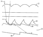
도 18은 도파관이 광을 바닥 표면을 향해 지향시키기 위한 반사체 구성요소에서 끝나는 하나의 실시예를 도시한다.
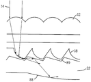
도 19는 도 18의 변형예를 도시하며, 여기서 집광기는 대칭 축을 중심으로 거울 대칭된다.
도 20은 도파관 및 방향전환 요소가 집광기에 대해 기울어진 도 13의 실시예의 한 형태를 도시한다.
도 21은 집광기 및/또는 방향전환 소자의 다양한 크기를 갖는 하나의 실시예를 도시한다.
도 22는 수광기를 대신해 광원을 이용한 광 확산을 위한 하나의 실시예를 도시한다.
도 23은 2개의 축을 가로지르는 집광을 얻기 위해 도 4의 실시예에 대한 서로 다른 변동을 도시한다.
도 24는 2개의 축을 가로지르는 집광을 얻기 위한 또 다른 실시예를 도시한다.
도 25는 본 발명의 태양 집광기의 상이한 실시예를 도시한다.
도 26는 본 발명의 태양 집광기의 상이한 실시예를 도시한다.
도 27는 본 발명의 태양 집광기의 상이한 실시예를 도시한다.
도 28은 본 발명의 집광기의 상이한 실시예를 도시한다.
도 29은 본 발명의 집광기의 상이한 실시예를 도시한다.
도 30은 본 발명의 집광기의 상이한 실시예를 도시한다.
도 31은 본 발명의 집광기의 상이한 실시예를 도시한다.
도 32은 본 발명의 집광기의 상이한 실시예를 도시한다.
도 33은 본 발명의 집광기의 상이한 실시예를 도시한다.
도 34은 본 발명의 집광기의 상이한 실시예를 도시한다.
도 35은 본 발명의 집광기의 상이한 실시예를 도시한다.
도 36은 본 발명의 집광기의 상이한 실시예를 도시한다.
도 37은 본 발명의 집광기의 상이한 실시예를 도시한다.
도 38은 엔트리 요소를 갖는 도파관을 도시한다.
도 39는 엔트리 요소를 갖는 도파관의 상이한 실시예를 도시한다.
도 40은 본 발명의 태양 집광기의 상이한 실시예를 도시한다.
도 41은 본 발명의 집광기의 상이한 실시예를 도시한다.
도 42는 본 발명의 집광기의 상이한 실시예를 도시한다.
도 43은 본 발명의 집광기의 상이한 실시예를 도시한다.
도 44는 본 발명의 집광기의 상이한 실시예를 도시한다.
도 45는 본 발명의 집광기의 상이한 실시예를 도시한다.
도 46은 중앙 축을 중심으로 하는 대칭을 갖는 본 발명의 태양 집광기의 상이한 실시예를 도시한다.
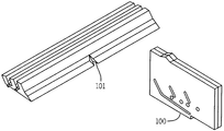
도 47은 위치설정 요소를 갖는 도 46의 압출도(extruded view)를 도시한다.
도 48은 횡단 광학 요소 및 위치설정 요소의 예를 도시한다.
도 49는 횡단 광학 요소를 갖는 도 46의 압출도를 도시한다. 1 illustrates a solar energy collector generally constructed in accordance with one embodiment of the present invention.
FIG. 2 shows a cross-sectional view of one embodiment of the optical waveguide shown schematically in FIG. 1.
FIG. 3 shows another cross-sectional view of a linear embodiment of the optical waveguide shown schematically in FIG. 1.
FIG. 4 shows another cross sectional view of a rotating embodiment of the optical waveguide shown schematically in FIG. 1.
5A shows the shape of the first edge of the reflective element of the waveguide.
5B shows the shape of the second edge of the reflective element of the waveguide.
5C shows a first discrete element for redirecting light as part of a stepped waveguide.
5D shows a second discrete element for diverting light as part of a stepped waveguide.
5E shows a system having a plurality of light pipes connected by stepped waveguides.
5F shows a waveguide with a built-in redirecting component.
6 shows a curved light collecting element and a curved reflector connected to a waveguide.
7 shows one curved light collecting element and two planar reflectors connected to the waveguide.
8A shows a closed optical element connected to the waveguide.
FIG. 8B shows an enlarged view of the junction of the optical element and waveguide of FIG. 8A.
9A shows another closed optical element connected to the waveguide, and FIG. 9B shows an enlarged view of the junction of the optical element and waveguide of FIG. 9A.
10A shows another closed optical element connected to the waveguide, and FIG. 10B shows an enlarged view of the junction of the optical element and waveguide of FIG. 10A.
FIG. 11A shows another closed element connected to the waveguide, and FIG. 11B shows an enlarged view of the junction of the optical element and waveguide of FIG. 11A.
12 shows the ray tracing results for the optical system of FIGS. 2 and 6-11.
13 shows another representation of an embodiment of a solar energy concentrator or illuminator.
14 illustrates a refractive concentrator component for a conventional system.
15 illustrates a reflective collector component for yet another conventional system.
Fig. 16 shows a casee grain condenser having a primary reflective optical element and a secondary reflective optical element.
FIG. 17 shows light transmittance versus light receiving angle for a system similar to FIG. 13.
18 illustrates one embodiment where the waveguide ends in a reflector component for directing light towards the bottom surface.
FIG. 19 shows a variant of FIG. 18, wherein the collector is mirror symmetric about an axis of symmetry.
FIG. 20 illustrates one form of the embodiment of FIG. 13 with the waveguide and the redirecting element tilted relative to the collector.
21 shows one embodiment with various sizes of the light collector and / or the redirecting element.
22 shows one embodiment for light diffusion using a light source in place of a light receiver.
FIG. 23 illustrates different variations for the embodiment of FIG. 4 to obtain condensing across two axes.
24 illustrates another embodiment for obtaining condensing across two axes.
25 shows a different embodiment of the solar collector of the present invention.
Figure 26 shows a different embodiment of the solar collector of the present invention.
Figure 27 shows a different embodiment of the solar collector of the present invention.
28 shows different embodiments of the light collector of the present invention.
29 shows different embodiments of the light collector of the present invention.
30 shows a different embodiment of the light collector of the present invention.
Figure 31 shows a different embodiment of the light collector of the present invention.
32 shows a different embodiment of the light collector of the present invention.
33 shows different embodiments of the light collector of the present invention.
34 shows different embodiments of the light collector of the present invention.
35 shows a different embodiment of the light collector of the present invention.
36 shows different embodiments of the light collector of the present invention.
37 shows different embodiments of the light collector of the present invention.
38 shows a waveguide with entry element.
39 illustrates a different embodiment of a waveguide with entry element.
40 shows different embodiments of the solar collector of the present invention.
Figure 41 shows a different embodiment of the light collector of the present invention.
42 shows different embodiments of the light collector of the present invention.
43 shows a different embodiment of the light collector of the present invention.
44 shows different embodiments of the light collector of the present invention.
45 shows different embodiments of the light collector of the present invention.
46 illustrates different embodiments of the solar collector of the present invention having symmetry about a central axis.
FIG. 47 shows the extruded view of FIG. 46 with a positioning element.
48 shows examples of transversal optical elements and positioning elements.
FIG. 49 shows the extrusion view of FIG. 46 with the transverse optical element.
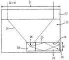
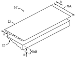
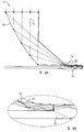
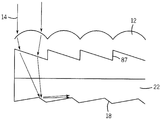
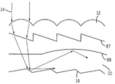
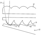
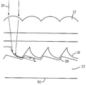
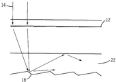
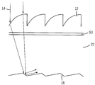
본 발명의 바람직한 실시예에 따라 구축된 태양 에너지 집광기 시스템은 도 1에서 개략적으로 (10)으로 나타내어진다. 태양 에너지 집광기 시스템(10)은 임의의 종래의 집광기, 가령, 대물 렌즈, 프레넬 렌즈(Fresnel lens)일 수 있는 광학 집광 요소(optical concentrating element)(12) 및/또는 반사 표면 요소, 가령, 포물선 형태 또는 복합 형태 반사체를 포함한다. 이 광학 집광 요소(12)는 입력 광(input light)(14)에 작용하여 광(14)을 작은 초점 영역(16)에 집광시킬 수 있다. 바람직한 실시예에서, 작은 초점 영역(16)은 반사 또는 방향전환(redirecting) 구성요소(18) 또는 내부 전반사를 야기하는 그 밖의 다른 종래의 광 방향전환 요소 내에 배치된다. 방향전환 구성요소(18)는 집광된 광(20)을 도파관(22)으로 방향전환시킨다. 도파관(22)은 스넬 법칙에 따라, 광(20)의 내부 반사를 일으켜 광(20)이 도파관(22)을 따라 전파되도록 구성되며, 여기서 도파관(22)의 표면(24)에 입사되는 광(20)의 각도가 임계각 ![]()
![]()
![]()
![]()
여기서, ![]()
![]()
η도파관 = 도파관 재료의 굴절률,η waveguide = refractive index of the waveguide material,
η클래딩 = 클래딩 층의 굴절률 또는, 주변/도파관 경계면에서의 굴절률η cladding = refractive index of the cladding layer or refractive index at the periphery / waveguide interface
수광기(26)가 도파관(22)의 단부에 배치되고, 유용한 에너지로 처리하기 위해, 또는 그 밖의 다른 광학적 이용을 위해, 광(20)을 수신한다. A
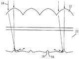
도 13은 시스템(10)의 바람직한 형태를 구체적으로 도시한다. 복수의(N개의) 집광 요소(12) 및 방향전환 요소(18)가 도시된다. 집광도 비(concentration ratio)=A/B이도록, 각각의 집광 요소(12)는 영역(A)으로부터 θ1의 반각(half angle)을 갖는 입력 광(14)을 취하고, 반각 θ2을 갖고 광(14)을 더 작은 영역(B)로 집광시킨다. 방향전환 요소(18) 각각은 집광 요소(12)들 중 연관된 하나로부터 집광된 광을 수신하여, 약간의 각도![]()
![]()
= 도파관의 높이 / 도파관의 길이= Waveguide height / waveguide length
= N×B/N×A= N × B / N × A
= B/A= B / A
= 1/각각의 요소 내 집광도 비 = 1 / condensing ratio in each element
압밀성(compactness)은 태양 집광기(및 그 밖의 다른 장치, 가령, 조명기(illuminator))에 대한 훌륭한 현실적인 이점을 가진다. 다른 이점들 중에서, 재료가 덜 사용되고, 어려운 밀봉이 요구되는 광소자와 수광기(23) 간의 큰 공기 간격이 제거되며, 장치의 부피가 훨씬 덜 커서 배송 및 설치 비용이 낮고, 비싸고 위험부담이 있는 커스텀 제조 방법보다 전통적인 플랫 모듈 제조 방법이 사용될 수 있다는 이점이 있다. Compactness has excellent practical advantages over solar concentrators (and other devices, such as illuminators). Among other advantages, a large air gap between the optical element and the
도파관(22)에 대한 압밀성의 한계는 수광기(23)에 의해 정의된다. 따라서 도파관(22)은 자신이 광을 전달하는 수광기(23)만큼만 압밀할 수 있다. 대부분의 집광기의 경우, 집광기(12)의 압밀성이 수광기(23)의 폭보다 상당히 더 크다. 그러나 이 장치는 자신에게 전달되는 집광된 광의 면적에 의해 정의되는 높이를 각각 갖는 섹션들로부터 도파관(22)을 구성하기 때문에, 합쳐진 도파관(22)은 수광기(23)의 폭과 동일한 높이를 가진다. 다시 말하면, 도파관(22)은 한계까지 압밀하다. The limit of consolidation on the
따라서 본 발명의 구성의 관점에서, 집광기 시스템(10)에 의해 얻어지는 광의 집광도는 종횡비 A/B의 함수이며, 매우 압밀한 집광기 시스템(10)을 도출한다. 상기 장치는 비교적 넓은 영역으로부터의 광을 집결시키고 상기 광을 압밀성을 유지하면서 연속 영역을 갖는 비교적 작은 수광기로 집광시킬 수 있다. 이는 필요한 재료의 부피를 감소시키고, 단일 몰드(mold)로부터 복수의 유닛이 만들어질 수 있게 하며, 조립 복잡도를 감소시킴으로써, 생산을 단순화시킨다. Therefore, from the viewpoint of the configuration of the present invention, the light condensing degree of light obtained by the
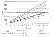
도 12는 도 2 및 6-11에 도시된 설계에서 수행되는 광선 추적(ray tracing)의 결과를 도시한다. 각각의 설계는, A/B의 비로 나타나는 바와 같은, 선형 차원으로 광을 집광시키는 능력 측면에서 특정 성능을 보인다. 데이터는 +-1도의 입력 원뿔 반각과 +-20도의 출력 원뿔 반각, n=1의 초기 굴절률, 및 n=1.5의 최종 굴절률을 갖는 광에 대한 것이다. 상기의 입력 파라미터일 때 이론적 최대 허용 가능한 광학 집광도는 선형 차원에서 30x이며, 반면에 예를 들어 도 9는 25x의 집광도 팩터(concentration factor)를 얻는다. 선형 차원에서의 집광도 팩터는 종횡비 A/B에 비례하기 때문에, 도 9에 도시된 설계는 길이(A)가 250밀리미터인 반면에 두께(B)는 10밀리미터에 불과한 집광기, 또는 길이(A)가 500밀리미터인 반면에 두께(B)는 20밀리미터에 불과한 집광기를 보여준다. 이는 비교적 넓은 영역으로부터 집광된 광을 효과적으로 집결시키고, 상기 광을 단일 수광기로 전달할 수 있는 매우 압밀한 집광기 시스템(10)을 나타낸다. FIG. 12 shows the results of ray tracing performed in the designs shown in FIGS. 2 and 6-11. Each design exhibits certain performance in terms of its ability to focus light in a linear dimension, as represented by the ratio of A / B. The data are for light with an input cone half angle of + -1 degrees and an output cone half angle of + -20 degrees, an initial refractive index of n = 1, and a final refractive index of n = 1.5. The theoretical maximum allowable optical concentration is 30x in the linear dimension with the above input parameters, whereas FIG. 9, for example, obtains a concentration factor of 25x. Since the condensing factor in the linear dimension is proportional to the aspect ratio A / B, the design shown in FIG. 9 has a length A of 250 millimeters while the thickness B is only 10 millimeters, or a length A Is 500 millimeters, while thickness (B) shows a condenser of only 20 millimeters. This represents a very
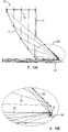
집광기(12)의 임의의 입구 구경(entry aperture)에 대해 집광 요소(12) 및 방향전환 요소(18)의 치수 및 개수는 달라질 수 있다. 예를 들어, 도 13에 도시된 시스템(10)은 크기는 절반(A/2 및 B/2)이고 개수는 2배(2×N)인 요소를 갖고 구성될 수 있다. 집광 요소(12) 및 방향전환 요소(18)가 더 작아지고 더 많아짐에 따라, 1/집광도 비로 나타나는 전체 집광기(12)의 종횡비는 도파관(22)의 종횡비에 근사한다. 다시 말하면, 10의 집광도 비의 경우, 집광기(12)의 종횡비는 0.1일 수 있다.For any entry aperture of the
집광기(12)에 대한 일반적인 종횡비는 1 정도이다. 도 14는 굴절형 집광기(12)를 도시하며, 상기 굴절형 집광기는 예를 들어 대물 렌즈 또는 프레넬 렌즈일 수 있다. 대물 렌즈의 초점 길이는 높이(25)를 정의한다. 집광도 비는 A/B로 나타나고, 종횡비는 높이/A로 나타나며, 이는 집광도 비보다 크다. 도 15는 반사형의 집광기(12)에 대한 유사한 경우를 보여준다.The general aspect ratio for the
단일 집광 요소에 대해 압밀성의 한계에 도달하기 위한 시도가 이뤄졌다. 도 16은 1차 및 2차 반사형 광소자로 구성된 카세그레인(Cassegrainian)식 집광기를 보여준다. 높이/A로 나타나는 종횡비는 0.25이다. 윈스톤(Winston)은 "Planar Concentrators Near the Etendue Limit", 2005에서 "1/4 종횡비의 기본적인 압밀성 한계(fundamental compactness limit of a 1/4 aspect ratio)"라고 기술했다. 본 발명의 맥락에서, 이 압밀성 한계는 개별 집광 요소(12)들에게 적용된다. 복수의 집광 요소(12)로부터 합쳐지는 도파관(22)을 사용함으로써, 시스템(10)의 압밀성이 ¼보다 낮아지게 되고, 1/집광도 비에 근사하게 된다.Attempts have been made to reach a limit of compaction for a single light collecting element. FIG. 16 shows a Cassgrainian condenser composed of primary and secondary reflective optical elements. The aspect ratio, expressed as height / A, is 0.25. Winston wrote in "Planar Concentrators Near the Etendue Limit", 2005, "fundamental compactness limit of a 1/4 aspect ratio." In the context of the present invention, this limit of compaction applies to the individual
본 발명은 또한, 입력에서부터 수광기(23)로 전달되는 광 에너지의 투과 효율(transmission efficiency)에서 이점을 가진다. 도 13에서, θ2는 집광 요소(12)에 의해 제어된다. 또한 θ2는 도파관(22)의 표면에 충돌하는 광에 의해 만들어진 각도가 되고, 90-θ2는 도파관 표면의 법선에 대한 각도이다. 앞서 설명된 바와 같이, θ2는 도파관(22) 내에서 내부 전반사를 얻도록 설정될 수 있어서, 표면 흡수 손실을 0까지로 감소시킨다.The invention also has an advantage in the transmission efficiency of the light energy transferred from the input to the
덧붙이자면, 이하의 특정 실시예에서 나타난 것처럼, 집광 요소(12) 및 방향전환 요소(18)는 내부 전반사를 이용해 광(14)을 조작하도록 설계될 수 있다. 또한 집광 요소(12) 및 방향전환 요소(18) 및 도파관(22)은 광(14)에 대해 고형 유전체 매질 내에에 연속 경로(contiguous path)를 제공하도록 구성될 수 있다. 다시 말하면, 입력 영역으로부터 수광기(23)로의 광선이 반사형 코팅 또는 굴절률의 변경에 결코 직면할 필요가 없다. 반사형 코팅은 ~8%의 흡수 손실을 야기할 수 있다. 굴절률 1.5의 광학 물질(플라스틱 또는 유리)로부터 공기로의 굴절률의 변화가 ~4%의 프레넬 반사 손실을 야기할 수 있다. 따라서 이들 손실 메커니즘에 대한 투과 효율은 100%에 근사할 수 있다.In addition, as shown in the specific embodiments below, the
이는 종래의 집광기 광소자와 다른 점이다. 반사형 광소자는 반사될 때 8% 손실률을 가질 것이다. 따라서 투과 효율은 단일 광소자에서 ~92%일 것이고, 2차 반사형 광소자가 사용될 때 ~85%일 것이다. 굴절형 광소자는 적어도 하나의 굴절률 변경을 필요로 한다. 따라서 투과 효율은 단일 광소자의 경우, ~96%일 것이고, 2차 굴절형 광소자가 사용될 때 ~92%일 것이다.This is different from the conventional condenser optical element. Reflective optical devices will have an 8% loss rate when reflected. Therefore, the transmission efficiency will be ~ 92% in a single optical device, and ~ 85% when a secondary reflective optical device is used. Refractive optical elements require at least one refractive index change. Therefore, the transmission efficiency will be ˜96% for a single optical device and ˜92% when a second refractive optical device is used.
도 17은 도 13에 도시된 발명의 실시예에 따라, 입력 반각 θ1의 함수로서의 투과율을 도시한다. 계산은 광선 추적 소프트웨어를 기초로 한다. 실시예는 +-3도의 입력 각 내에서 기능하도록 설계되었다. 효율은 프레넬 반사율 및 하드 반사율로부터의 손실을 고려한다. 나타난 것처럼, 장치의 효율은 θ1=0에서 100%에 근사하며, +-3도 내에서 거의 100%를 유지하고, 그 다음에 가파르게 낮아진다. FIG. 17 shows the transmittance as a function of the input half-angle θ 1 , according to the embodiment of the invention shown in FIG. 13. The calculation is based on ray tracing software. The embodiment is designed to function within an input angle of + -3 degrees. Efficiency takes into account losses from Fresnel reflectance and hard reflectance. As shown, the efficiency of the device is close to 100% at θ 1 = 0, and maintains nearly 100% within + -3 degrees and then drops steeply.
도 2에 도시된 집광기 시스템(10)의 또 다른 선호되는 형태에서, 입사광(14)은 본원에 기재된 요소(12)를 이용해 제 1 계단에서 집광 또는 포커스된다. 집광된 광(20)은 집광기 시스템(10)의 섹션을 반사체/도파관 섹션(28)과 연관시킴으로써 추가로 처리된다. 반사체/도파관 섹션(28) 각각은 집광된 광(20)을 수신하고, 연관된 도파관 섹션(28) 내에서 광(30)을 방향전환시키는 반사형 섹션(32)을 포함하며, 여기서, 전체 도파관(22)의 길이 방향을 따라 내부 전반사(TIR: total internal reflection)를 겪는다. 복수의 반사체/도파관 섹션(28)은 도파관(22)을 포함하고, 계단형의 도파관 구조를 형성한다. In another preferred form of the
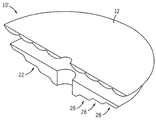
도 18은 도파관(22)이 반사체(27)에서 끝나고, 반사체(27)가 광(14)을, 수광기(23)가 위치할 수 있는 도파관(22)의 바닥 표면 쪽으로 방향전환시키는 시스템(10)의 또 다른 실시예를 도시한다. 집광기 광소자가 수광기(23)를 구현하는 종래의 수광기 요소의 평면 상으로 편평하게 놓이는 것이 제조상 이점일 수 있다.18 shows a
이러한 구성을 이용할 때, 어느 한 단부에서 두 개의 수광기(23)가 하나의 단일 수광기(23)가 배치될 수 있는 하나의 연속 영역을 형성하도록, 집광기(12)는 도 19에 도시된 것처럼 대칭축을 중심으로 거울 대칭될 수 있다. 이러한 경우, 개구부 면적은 두 배가 되지만 집광기(12)의 두께는 변하지 않기 때문에, 압밀성의 한계는 1/(2×집광도 비)에 의해 표현된다.Using this configuration, the
방향전환 요소(18)는 각도 ![]()
![]()
![]()
![]()
![]()
![]()
집광 요소(12)와 방향전환 요소(18) 및 이들과 연관된 도파관의 크기도 달라질 수 있고, 도 21은 이에 대한 예시를 보여준다. 여기서, A1, A2, 및 A3은 상이한 길이를 가지며, B1, B2 및 B3도 상이한 길이를 가진다. 그러나 집광도 비는 각각의 섹션에서 동일하게 유지된다: A1/B1 = A2/B2 등등. 따라서 도파관(22)의 종횡비는 다음의 식에 의해 표현된다: The size of the
= (Bl + B2 + B3) / (Al + A2 + A3) = (Bl + B2 + B3) / (Al + A2 + A3)
= 1 / 집광도 비 = 1 / light intensity ratio
도 22에 도시된 또 다른 실시예에서, 또한 시스템(10)은 광(31)을 역방향으로 통과시킴으로써, 산광기로서 사용될 수도 있다. 도 22에서 본래는 수광기(23)인 광원(33)으로부터 입력되는 광은 도파관(22)을 통과하며, 방향전환 요소(18)에 의해 집광 요소(12) 상으로 방향전환되며, 상기 집광 요소는 출력 광을 시스템(10) 위로 전달한다. 적용예는 조명(illumination), 배면 조명(backlighting), 및 그 밖의 다른 산광 장치를 포함한다. 광의 집광을 위해 예로 든 광소자가 조명을 위해서도 사용될 수 있고, 이때, "수광기(23)"가 광원으로 대체됨을 이해해야 한다. In another embodiment shown in FIG. 22, the
다양한 반사체/도파관 섹션(28)의 횡단면은 집광기 시스템(10)의 다양한 구성에 대한 기본 빌딩 블록을 제공한다. 종횡비 N×B/N×A, A/B, A/B에 비례하는 면적 집광도 팩터 또는 에너지 밀도 Δ![]()
![]()
도 4는 도파관(22)의 반사체/도파관 섹션(28)과 연관된 집광기 시스템(10') 및 집광 요소(12)를 갖는 회전(또는 축) 대칭적 지오메트리의 형태로 된 집광기 시스템(10)의 또 다른 예시를 도시한다. 원의 일부분일 수 있는 이러한 회전 대칭적 형태의 집광기 시스템(10')(또는 시스템(10))은 입사광(14)의 3차원 방사형 수렴이 (A/B)2에 비례하는 집광도 비 Δ![]()
![]()
도 4는 2개의 축에 걸친 집광도를 얻기 위한 한 가지 방법을 도시하며, 도 23은 또 다른 방식을 도시한다. 여기서 선형 대칭 1차 집광기(12)는 하나의 축을 따라 집광되는 광을 집광기(12)의 측부에 있는 자신의 수광기(23)로 전달한다. 이때, 2차 선형 대칭 집광기(37)는 수직 축으로 위치한다. 이 2차 집광기(37)는 제 2 축을 따라 광을 집광시켜 최종 수광기(23)로 광을 전달한다. 4 shows one method for obtaining the degree of condensation across two axes, and FIG. 23 shows another way. The linear symmetric
도 24는 두 축에 걸쳐 집광도를 얻기 위한 세 번째 방식을 도시한다. 여기서 도시된 집광기(12)는 도 19에 도시된 것처럼 거울 대칭을 가진다. 다시 말하면, 선형 대칭 1차 집광기(12)는 하나의 축을 따라 집광된 광(14)을, 집광기(12)의 바닥에 있는 자신의 수광기(23)로 전달한다. 따라서 2차 선형 대칭 집광기(37)가 수직 축으로 위치한다. 이 2차 집광기(37)는 광(14)을 두 번째 축을 따라 집광시키고, 광을 최종 수광기(23)로 전달한다. 24 shows a third way to obtain the degree of condensing across two axes. The
도 3 및 4의 선형 및 회전 실시예에 추가로, 집광기 시스템(10')은 입사광(14)의 방향에 대해 도파관(22) 위 및/또는 아래에 배치될 수 있다. 이러한 실시예에서, 광(14) 중 일부는 도파관(22)을 통과할 것이고, 집광기 시스템(10')에 의해 방향전환되어 도파관(22)으로 되돌아 올 것이다. 이들 형태의 시스템은 광 재활용을 가능하게 하고, 따라서 본원에 기재된 집광을 위한 반사형 시스템의 최종 효율 및 사용을 개선하고, 종래의 굴절형 시스템에 비해 광의 집광에 대해 증가된 효율을 보인다. In addition to the linear and rotational embodiments of FIGS. 3 and 4, the
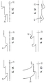
또 다른 실시예에서, TIR을 야기하기 위해 반사형 요소(18)는 도파관(22)에 대해 각도 조절될 수 있다. 상기 반사형 요소(18)는 다양한 다각 프로파일을 갖는 도파관(22)의 일체 부분일 수 있다(도 5A 및 5B 참조). 요소(18)는 또한 요소(38 및 39)로부터 분리될 수 있다(도 5C 및 5D 참조). 덧붙여, 반사형 요소(18) 및 이와 연관된 도파관(22)은 도 5E 및 5F에서 각각 나타난 복잡한 광 수집기 파이프(42) 및 광 방향전환 구성요소(43)의 형태를 취할 수도 있다.In another embodiment,
앞서 기재된 형태의 집광기 시스템(10 및 10')은 집광된 광(20)을 분절 영역과 대비되는 연속 영역으로 제공하며, 이로써, 집광된 태양 에너지가 다양한 다운스트림 수광기(26), 가령, 태양 전지, 추가 처리를 위한 광 파이프, 열 교환기, 2차 집광기, 및 광 스펙트럼 스플리터로 전달된다.
도 6-11B에 나타난 또 다른 일련의 실시예에서, 다양한 광학 구성요소들이 조합 사용되어 집광 및 수집 효율 모두를 추가로 그리고 실질적으로 개선할 수 있다. 가장 바람직한 실시예에서 도 6은 광(52)을 곡선형 반사체(54) 상으로 지향시키는 곡선형의 집광 요소(50)를 도시하며, 상기 곡선형 반사체(54)는 광(52)을 도파관(22)으로 통과시킨다. 또 다른 가장 바람직한 실시예에서 도 7은 또 다른 곡선형 집광 요소(56)를 도시하며, 상기 곡선형 집광 요소(56)는, TIR에 의해 광(52)을 도파관(22) 내로 방향전환시키는 두 개의 편평한 표면(59 및 60)을 갖는 반사체(58)로부터 광(52)을 지향시킨다. 도 8A는 계면(66)에서 광(52)을 방향전환시키고, 곡선형 반사체(68)로부터의 광(52)을 반사시켜 광(52)을 광학 요소(64)의 하부 반사 표면(72) 사이의 계면(70)으로 포커싱하는 부분 폐쇄된 광학 요소(64)를 도시한다. 도 8B의 확대도로 잘 나타나 있는 것처럼, 도파관(22)은 반사 표면(72)과 실질적으로 상보적인 다각 정합을 가진다.In another set of embodiments shown in FIGS. 6-11B, various optical components can be used in combination to further and substantially improve both light collection and collection efficiency. In the most preferred embodiment, FIG. 6 shows a curved light collecting element 50 that directs light 52 onto
도 9A의 또 다른 바람직한 실시예는 광학 요소(65)가 폐쇄되고 (광 파이프의 형태로 된) 확장 도파관(74)으로 연결되며, 상기 확장 도파관(74)은 광(52)을 수집하고 이를 도파관(22) 내로 전달(도 9B에서 가장 잘 나타남)한다는 것을 제외하고 도 8A의 실시예와 유사하다.Another preferred embodiment of FIG. 9A is that
도 10A에서 광학 요소(76)는 도 10B에 가장 잘 나타난 특정 다각형 횡단면을 갖는 반사 표면(77)으로부터의 TIR에 의해 반사된 입력 광(52)에 의해 폐쇄되며, 상기 특정 다각형 횡단면은 TIR로부터의 광의 수집을 가능하게 하고 표면(80, 81 및 82)으로부터의 반사에서부터 도파관(22)으로의 연결을 가능하게 한다.In FIG. 10A
도 11A에서, 두 개의 상이한 광원(82 및 84)으로부터 광(52)을 도파관(22) 내로 지향시키기 위해, 광학 요소(82)는 또 다른 반사체(84)와 협업하고, 따라서 광학 요소(82)의 표면(86)에 입사하는 모든 광의 수집이 추가로 보장된다. 이 실시예에서, 광학 요소(82 및 84)는 집광 요소와 반사 요소 모두의 역할을 수행한다.In FIG. 11A, to direct light 52 from two
도 25에서, 곡선형 집광 요소(12)는 광(14)을 방향전환 구성요소(18) 상으로 지향시키고, 상기 방향전환 구성요소(18)는 광(14)을 도파관(22) 내부로 전달한다. 집광 요소(12) 및 방향전환 구성요소(18)는 동일한 물리적 부분 상의 두 개의 서로 다른 특징부로서 나타나며, 도파관(22)은 첫 번째 물리적 부분에 연결된 두 번째 물리적 부분으로 나타난다. 도 26에서 곡선형 집광 요소(12)는 광(14)을 시퀀스로 동작하는 두 개의 반사체(방향전환 구성요소(18)) 상으로 지향시키며, 상기 반사체는 광(14)을 도파간(22) 내부로 전달한다. 집광 요소(12), 방향전환 구성요소(18), 및 도파관(22)은 모두 다 함께 연결된 개별적인 물리적 부분으로 나타난다. 도 27은 도 26과 유사하게, 광(14)을 도파관(22) 내부로 지향시킨다. 그러나 방향전환 구성요소(18) 및 도파관(22)은 하나의 구조물로 조합된다. In FIG. 25, the curved
도 28에서, 굴절형 집광 요소(12)는 광(14)을 방향전환 요소(18) 내부로 지향시키고, 상기 방향전환 요소(18)는 광(14)을 도파관(22) 내부로 반사시킨다. 방향전환 요소(18)는 증분형 계단 특징부로서 도파관 구조물에 일체 구성되는 것이 바람직하다. 도 29에서, 도파관(22)이 자신의 길이 방향을 따라 실질적으로 균일한 횡단면 두께를 가지도록, 도파관(22)의 상부 표면이 기울어져 있는 것을 제외하고, 집광 요소(12) 및 방향전환 요소(18)는 도 28에 도시된 것과 유사하다.In FIG. 28, refracting
도파관이 집광 요소(12)의 평면에 실질적으로 평행이도록 방향전환 요소(18) 및 도파관(22)이 회전하는 것을 제외하고, 도 30은 도 29와 유사하다. 방향전환 요소(18)에 대한 광의 입사각이 도 30의 비교되는 광의 입사각보다 크도록, 집광 요소로부터의 광을 굴절시키는 방향전환 요소(87)의 추가 설정을 제외하고, 도 31은 도 30과 유사하다. 이는, 예를 들어, 방향전환 요소(18)에 대한 방향전환의 메커니즘으로서 내부 전반사를 더 잘 촉진시킨다. 도파관(22)의 상부 표면이 맞춤 구성된 형태(tailored shape)(88)인 것을 제외하고, 도 32는 도 31과 유사하다. 상기 맞춤 구성된 형태(88)는, 예를 들어, 도파관을 통해 지정된 스팟, 또는 도파관(22)의 단부의 위치 L로 전파하는 광을 전달하는 데 유용하다.FIG. 30 is similar to FIG. 29 except that the redirecting
도 33에서, 방향전환 요소(18)는 집광 요소(12) 및 도파관(22)을 운반하는 부분들과 별개인 단일 부분으로 일체 구성된다. 방향전환 요소(18)는 본원에서 앞서 언급된 임의의 유형을 가질 수 있고, 도 6에 나타난 것과 유사한 곡선형 반사형 요소로서 나타난다. 도파관(22)은 방향전환 요소(18)로부터의 광을 수신하도록 위치 설정된 증분형 계단(incremental step) 특징부(89)로 구성된다. 도파관(22)이 자신의 길이 방향을 따라 실질적으로 균일한 횡단면 두께를 갖도록 도파관(22)의 바닥 표면(90)이 기울어진 것을 제외하고, 도 34는 도 33과 유사하다. 도 35 및 36은 도파관(22)의 바닥 표면이, 각각 평평한 면(88) 및 곡선형 요소(88)로 나타나는 맞춤 구성된 형태(88)를 가짐을 보여준다. 도 32에 나타난 것처럼, 맞춤 구성된 형태(88)는 도파관(22)을 통해 도파관(22)의 단부의 지정된 스팟 L로 전파되는 광을 전달하는 데 유용하다. In FIG. 33, the redirecting
집광 요소(12)가 프레넬 렌즈(Fresnel lens)라는 것을 제외하고, 도 37은 도 30과 유사하다. 상기 프레넬 렌즈는 예를 들어 폴리머 물질 또는 공정에 적합한 그 밖의 다른 물질의 사출 성형(injection molding), 고온 엠보싱(hot embossing) 또는 미소복제(microreplication)에 의해 제조될 수 있다. FIG. 37 is similar to FIG. 30 except that the
도 38은 도 33-36에 도시된 것과 유사한 상부 표면 상의 엔트리 요소(91)를 갖는 도파관(22)을 도시한다. 엔트리 요소(91)가 개별 부분으로서 일체 구성되고, 그 후 광학 결합 층(92)을 통해 벌크 도파관 요소(22)의 편평한 상부 표면에 광학적으로 연결되는 것을 제외하고, 도 39는 유사한 도파관(22)을 도시한다. 따라서 광 엔트리 요소는 도파관의 본체로부터 물질적으로 불연속하게 배치된다. 이로써, 예를 들어 박막 기판을 기반으로 하는 제조 공정의 사용이 엔트리 요소 특징부를 만들 수 있다. 도 40은 완전 광학 설계의 일례 내에서 동작하는 도 39에 도시된 도파관(22)을 도시한다. 집광 요소(12)는 광(14)을 방향전환 요소(18) 상으로 집광시키려 상기 방향전환 요소(18)는 광(14)을 방향전환시켜, 엔트리 요소(91)를 통해 도파관(22) 내부로 삽입한다.FIG. 38 shows waveguide 22 with
집광 요소(12)를 포함하는 부분이 저율 접착제(low index adhesive)(93)를 이용해 도파관(22)으로 광학적으로 연결된다는 것을 제외하고, 도 41은 도 30과 유사하다. 이 구성은 집광 요소(12) and 도파관(22) 사이의 공극(air gap)을 제거하고, 따라서 집광 요소(12)에서 도파관(22)으로 광이 진행할 때 프레넬 반사 효과로 인한 광학 손실을 약화시킨다. 내부 전반사를 이용한 도파관(22) 내 광의 전파를 가능하게 하기 위해, 상기 저율 접착제(93)는 도파관(22)의 굴절률보다 낮은 적절한 굴절률을 가질 필요가 있다. 예를 들어, 저율 접착제(93)는 실리콘계 엘라스토머, 가령, Dow Corning Sylgard 184일 수 있다. 집광 요소(12)가 비대칭 벌크 렌즈 대신 프레넬 렌즈인 것을 제외하고 도 42는 도 41과 유사하다. FIG. 41 is similar to FIG. 30 except that the portion comprising the
도 43에서, 집광 요소(12)는 광(14)을 제 1 방향전환 요소(87)로 지향시키고, 상기 제 1 방향전환 요소(87)는 광(14)을 제 2 방향전환 요소(18) 상으로 지향시키면서 광(14)을 굴절시키며, 상기 제 2 방향전환 요소(18)는 광을 도파관(22) 내로 방향전환시켜 전파시킨다. 도 43에서, 제 1 방향전환 요소(87)는 편평한 면이다. 제 1 방향전환 요소(87)가 집광 요소(12)보다 앞서 광(14)과 상호작용한다는 것을 제외하고, 도 44는 도 43과 유사하다. 도 45에서, 도파관(22)은 자신의 길이 방향을 따라 광(14)을 2방향으로 또는 다중 방향으로 전파한다. 집광 요소(12)는 광을 방향전환 요소(18 및 94) 상으로 집광시키며, 두 개의 방향전환 요소(18 및 94)는 광을 반대 방향으로 도파관(22) 내부로 방향전환시킨다. 이 구성에 의해, 도파관(22)의 양 단부 모두에서 광이 집광되고 수집된다. In FIG. 43,
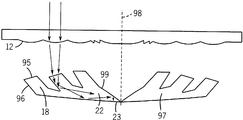
도 46에서, 집광 요소(12)는 광(14)을 방향전환 요소(18) 상으로 집광시킨다. 방향전환 요소(18)는 2개의 부분, 즉, 광을 벌크 광소자로 굴절시키는 편평한 면(95), 및 광을 도파관(22)으로 반사시키는 또 다른 편평한 면(96)을 가진다. 방향전환 면(95 및 96)과 도파관(22)은 하나의 단일 부분으로 일체 구성된다. 앞서 단락 [0059]에서 이전에 기재된 것처럼 도파관의 단부는 광을 수광기(23) 쪽으로 하향 방향전환시키는 면(99)을 가진다. 이 실시예에서, 도파관(22)은 축(98)을 중심으로 하는 거울 이미지로서, 도파관(97)을 가진다. 도파관(22)의 단부에 있는 2차 광소자의 배치 및 도파관(22)의 대칭 레이아웃은 본 출원에서 제시되는 모든 실시예와 함께 구현될 수 있고, 앞서 [0049]에서 설명된 바 있다.In FIG. 46, the
도 1-46에 기재된 방향전환 요소(18)는 대응하는 집광 요소(12)와 연관되고, 반사, 내부 전반사, 및 굴절의 광학 메커니즘 중 적어도 하나를 이용해, 도파관(22) 내로 광을 전달한다. 그러나 방향전환 요소가 집광 요소와 광학적으로 연결되고 물리적으로 분리될 필요는 없다.The redirecting
본 출원에 기재된 다양한 실시예에서, 집광 요소(12)는 층에 의해 연관된 방향전환 요소(18)의 적어도 일부분으로부터 분리된다. 광(14)은 이 층 내에서 어떠한 방향의 재배치 변경도 겪지 않는다. 상기 층 자체는 연관된 방향전환 요소(18) 각각의 적어도 일부분들 사이에서 연속이다. 이러한 층 분리에 의해, 집광 요소(12)와 방향전환 요소(18)가 물리적으로 개별적인 구성요소들의 수직 스택으로 배치될 수 있다. 이로써, 전체 태양 집광기를 형성하기 위해, 개별적인 부분들의 직접 조립이 가능해진다.In various embodiments described in this application, the
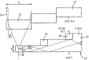
비용을 최소화하고 설계를 간소화하기 위해, 한 가지 현실적인 과제는 강건한 재료와 함께 가능한 적은 부분들로 앞서 기재된 모든 기능을 얻어야 한다는 것이다. 일반적으로 이는 복수의 기능을 단 몇 개의 부분에 포함시키는 것을 포함한다. 예를 들어, 커버유리(coverglass)에 광학 특징부를 패터닝함으로써, 다양한 광학 코팅을 위한 기판으로서 기능하는 유리의 능력을 보존하면서, 유리가 모듈을 보호하면서 집광 요소로서 동작하는 것이 실현 가능하다. 연화된 유리에, 기계 가공된 동심 특징부를 갖는 원통형 금속 롤(roll)을 적용함으로써, 대형 유리 제조 설비가 시트의 하나의 측부 상에 마일드 렌즈 특징부를 일상적으로 형성할 수 있다. 광학 특징부를 각인하기 위한 적절한 롤 설계가 주어지면, 1차 광학(집광) 요소(12)를 형성하기 위해, 선형 렌즈가 커버유리 상에서 패터닝될 수 있다. 상기 집광 요소(12)는 기능을 보존하면서 외향 및 내향 모두로 배향될 수 있다. 외향 특징부는 광 투과성에 유해한 입자 축적(particulate accumulation), 즉, 오염(soiling)의 위험을 무릅쓴다. 가공된 커버유리 방식에 추가로, 역시 집광 기능을 제공하는 실리콘계 증착과 같은 공정을 이용해, 특징부가 편평한 커버유리에 추가될 수 있다. In order to minimize costs and simplify the design, one realistic challenge is to get all the functions described above in as few parts as possible with robust materials. Typically this involves including a plurality of functions in just a few parts. For example, by patterning optical features on coverglass, it is feasible to operate the glass as a light collecting element while protecting the module while preserving the glass's ability to function as a substrate for various optical coatings. By applying a cylindrical metal roll with machined concentric features to the softened glass, large glass manufacturing equipment can routinely form mild lens features on one side of the sheet. Given the appropriate roll design for engraving optical features, a linear lens can be patterned on the coverglass to form the primary optical (condensing)
더욱이, 커버유리 층으로부터 집광된 광(14)에 대해 방향전환 요소(18)로서 기능하고, 방향전환된 광(14)을 수광기(23)로 전달하기 위한 도파관(22)으로서 기능하는 보완적 2차(secondary) 광학 부분을 구성하는 것이 가능하다(도 46). 이 실시예에서, 주(primary) 광소자는 보호성 커버유리와 집광 층 모두로서 기능하고, 2차 광소자에서 방향전환 기능과 도파관 기능이 조합될 수 있다. 마찬가지로, 점-포커스(point-focus) 설계의 경우, 고온 엠보싱 또는 성형(mold)-유형 공정을 이용해, 축방향 대칭 렌즈 패턴이 유리에 제공될 수 있다. Moreover, complementary, which acts as a redirecting
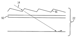
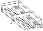
광학 기능을 커버유리에 포함시키고 방향전환 기능과 도파관-초점 영역 기능을 하나의 부분으로 조합하는 것에 의해, 단 2개의 부분에 의해서 전체 광학 경로가 관리되거나 얻어질 수 있다. ATIR의 이 2-부분 분류의 한 가지 중요한 양태는 도파관 또는 2차 광소자의 수직 부분과 수평 부분 모두 1차 광학 층(커버유리)에 비해 잘 유지되어야 한다는 것이다. 다른 관점에서, 분리 층의 지오메트리를 유지하는 것이 강건한 기능을 보장하는 데 중요하다. 이를 이루기 위한 한 가지 방법은 또 다른 기능을 1차 또는 2차/도파관 광학 부분 내에 포함시키는 것이다. 예를 들어, 도 47에 도시된 것처럼, 위치설정 요소, 즉, 리브(rib) 특징부(100)를 2차 광소자내로 포함시킴으로써, 안정적인 분리를 보장하기 위해 1차 광학 부분과 2차 광학 부분을 수직 차원과 수평 차원 모두에서 제한(constrain)하면서, 상기 1차 광학 부분과 2차 광학 부분을 기계적으로 상호체결(interlock)시키는 것이 가능하다. 따라서 위치설정 요소(100)는 수평, 수직, 및 회전 평면에서, 복수의 광학 요소와 도파관 간의 기하학적 관계(geometrical relationship)를 유지한다.By incorporating the optical function into the coverglass and combining the redirection function and the waveguide-focus area function into one part, the entire optical path can be managed or obtained by only two parts. One important aspect of this two-part classification of ATIR is that both the vertical and horizontal portions of the waveguide or secondary optical element must be well maintained relative to the primary optical layer (cover glass). In other respects, maintaining the geometry of the separation layer is important to ensure robust functionality. One way to accomplish this is to incorporate another function into the primary or secondary / waveguide optics. For example, as shown in FIG. 47, by including a positioning element, i.e.,
또 다른 생산 선택사항은 개별적으로 지지하는 위치설정 요소 즉 리브 특징부(100)를 생산하는 것이다. 이 선택사항은 또 다른 개별 부분을 만들어야 하는 단점을 지닌다. 그러나 리브 특징부는 매우 단순하여, 이 부분을 성형(mold)하기 위한 툴링 비용이 낮을 수 있고, 조립체는 모듈성을 더 갖게 된다(리브와 2차 광학 부분이 조립되는 방식으로 설계 유연성이 가능해 진다). 도 48은 보완적 광학 2차 지지 리브 특징부(100)를 도시한 영상을 도시한다. 이들 부분들은 설계 유연성을 제공하기 위해 모듈식으로 조립될 수 있다. 따라서 위치설정 요소(100)는 도파관의 일체형 부분 또는 도파관으로부터 분리되어 있는 요소일 수 있다.Another production option is to produce the individually supporting positioning elements, ie rib features 100. This option has the disadvantage of creating another separate part. However, the rib features are very simple, so the tooling cost to mold these parts can be low, and the assembly is more modular (allowing design flexibility by the way the rib and secondary optical parts are assembled). 48 shows an image showing the complementary optical secondary
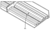
실현 가능한 수광기는 복수의 이산 광기전 태양 전지로 구성될 확률이 크다. 태양 전지들을 다 함께 연결할 때, 솔더 접합부 주변에 응력 집광을 관리하고 전지 파손을 최소화하기 위해 전지들 사이에 틈새(gap)를 남겨두는 것이 바람직하다. 이들 틈새의 효과는 광 에너지가 수집될 수 있는 영역을 감소시키는 것이다. 이들 틈새는 비-광학-활성 지지 특징부, 가령, 위치설정 요소 즉 리브(100)를 위치설정하기 위한 유용한 곳이다. 또한 광소자는 광학 방향전환 요소 또는 노치(notch) 특징부(101)에 의해 개조되어, 다른 경우라면 틈새 상으로 왔을 광의 대부분을 활성 수광기 쪽으로 지향시키도록 할 수 있다(도 49). 노치 특징부(101)는 방향전환 요소와 유사하지만 도파관(22)의 상이한 평면으로 배향되어, 광을 갭으로부터 활성 수광기 상으로 내부 반사시킬 수 있다. 노치 또는 횡단 광학 요소(101)는 도파관(22)으로 연결되고, 광을 도파관(22) 내에서 광의 전파 방향과 교차하는 방향으로 방향전환시킨다. 앞서, 도파관과 연결되고, 도파관에서부터 수광기로 광을 방향전환시키는 2차 광학 요소(27)가 기재되었다. 앞서 언급된 횡단 광학 요소(101)가 사용될 때, 2차 광학 요소(27)는 도파관으로부터 그리고 횡단 광학 요소로부터 수광기로 광을 방향전환시킨다.A feasible receiver is likely to consist of a plurality of discrete photovoltaic solar cells. When connecting the solar cells together, it is desirable to leave gaps between the cells to manage stress collection around the solder joint and minimize cell breakage. The effect of these gaps is to reduce the area where light energy can be collected. These gaps are useful for positioning non-optical-active support features, such as positioning elements, ie
본 발명의 실시예에 대한 상기의 기재는 설명과 기재의 목적으로 제공되었다. 이는 본 발명을 총 망라한 것은 아니며, 본 발명을 개시된 구체적인 형태로 한정하지 않고, 상기의 설명의 관점에서 수정 및 변형이 가능하고, 본 발명의 실시로부터 얻어질 수 있다. 다양한 실시예에서, 그리고 특정 용도에 적합할 때 다양한 변형예로, 해당 분야의 통상의 기술자가 본 발명을 이용하기 위해, 실시예들은 본 발명의 원리 및 그 실제 적용을 설명하기 위해 선택 및 기재되었다.
The foregoing description of the embodiments of the invention has been presented for the purposes of illustration and description. It is not intended to be exhaustive or to limit the invention to the precise forms disclosed, and modifications and variations are possible in light of the above teachings and may be obtained from practice of the invention. In various embodiments, and in various variations when suitable for a particular use, for those skilled in the art to use the invention, the embodiments have been selected and described to illustrate the principles of the invention and its practical application. .
Claims (18)
서로 인접하게 배치된 복수의 광학 요소
를 포함하고, 상기 복수의 광학 요소 각각은,
a) 광을 수집하고 재배치하기 위한 집광 요소(concentrating element), 및
b) 상기 집광 요소로부터의 광을 수신하기 위해, 상기 집광 요소와 연관되고 상기 집광 요소로부터 분리되어 있는 연관 방향전환 요소(redirecting element)
를 포함하며, 복수의 광학 요소의 각각의 집광 요소는 층에 의해 연관 방향전환 요소의 적어도 하나의 부분으로부터 분리되어 있고, 상기 층 내에서 광은 방향의 재배치 변화를 겪지 않고, 상기 층은 연관 방향전환 요소들 각각의 적어도 일부분들 사이에서 연속(contiguous)이며, 상기 광학 집광기는
연관 방향전환 요소의 적어도 하나의 부분으로부터의 광을 수신하기 위한 계단형 도파관 - 상기 연관 방향전환 요소의 적어도 하나의 부분은 광을 계단형 도파관 내부로 재배치하여 집적(accumulation)되게 하도록 구성됨 - ;
계단형 도파관으로 연결되어 있으며, 도파관으로부터의 광을 수광기 쪽으로 방향전환시키는 2차 광학 요소; 및
계단형 도파관으로부터의 광을 수신하기 위한 수광기(light receiver)
를 포함하는, 광학 집광기. As an optical concentrator, the optical concentrator
A plurality of optical elements
Includes, each of the plurality of optical elements,
a) a concentrating element for collecting and relocating light, and
b) an associated redirecting element associated with and separate from the light collecting element for receiving light from the light collecting element.
Wherein each condensing element of the plurality of optical elements is separated from the at least one portion of the associative redirecting element by a layer, in which light does not experience a rearrangement change in direction, wherein the layer is in an associative direction Between at least portions of each of the switching elements is contiguous, the optical concentrator
Stepped waveguide for receiving light from at least one portion of the associated redirecting element, wherein at least one portion of the associated redirecting element is configured to rearrange and accumulate light into the stepped waveguide;
A secondary optical element connected by a stepped waveguide and redirecting light from the waveguide toward the light receiver; And
Light receiver for receiving light from a stepped waveguide
Including, an optical condenser.
서로 인접하게 배치된 복수의 광학 요소
를 포함하고, 상기 복수의 광학 요소 각각은,
a) 광을 수집하고 재배치하기 위한 집광 요소(concentrating element), 및
b) 방향전환 요소(redirecting element)
를 포함하며, 상기 방향전환 요소는, 1) 집광 요소로부터의 재배치된 광을 수신하고 상기 광을 제 2 방향전환 요소 상으로 굴절시키는 제 1 방향전환 요소와, 2) 제 1 방향전환 요소로부터의 광을 수신하고 반사를 통해 광을 재배치하는 제 2 방향전환 요소를 포함하며, 복수의 광학 요소 각각의 집광 요소는 층에 의해 연관 방향전환 요소의 적어도 하나의 부분으로부터 분리되어 있으며, 상기 층 내에서 광은 방향의 재배치 변화를 겪지 않고, 상기 층은 연관 방향전환 요소 각각의 적어도 일부분들 사이에서 연속이고, 상기 광학 집광기는
연관 방향전환 요소의 적어도 하나의 부분으로부터의 광을 수신하기 위한 계단형 도파관 - 상기 연관 방향전환 요소의 적어도 하나의 부분은 광을 계단형 도파관 내부로 재배치하여 집적(accumulation)되게 하도록 구성됨 -
을 더 포함하는, 광학 집광기. As an optical condenser, the optical condenser
A plurality of optical elements
Includes, each of the plurality of optical elements,
a) a concentrating element for collecting and relocating light, and
b) redirecting element
Wherein the redirecting element comprises: 1) a first redirecting element that receives relocated light from the light collecting element and refracts the light onto a second redirecting element; and 2) from the first redirecting element. A second redirecting element that receives light and repositions the light through reflection, wherein the light collecting element of each of the plurality of optical elements is separated from the at least one portion of the associated redirecting element by a layer, within the layer The light does not undergo a rearrangement change in direction, and the layer is continuous between at least portions of each of the associated redirecting elements and the optical concentrator
Stepped waveguide for receiving light from at least one portion of the associated redirecting element, wherein at least one portion of the associated redirecting element is configured to rearrange and accumulate light into the stepped waveguide
It further comprises an optical condenser.
서로 인접하게 배치된 복수의 광학 요소
를 포함하고, 상기 복수의 광학 요소 각각은,
a) 광을 수집하고 재배치하기 위한 굴절 집광 요소(refracting concentrating element), 및
b) 상기 집광 요소로부터의 광을 수신하기 위해, 상기 집광 요소와 연관되고 상기 집광 요소로부터 분리되어 있는 연관 방향전환 요소(redirecting element)
를 포함하며, 복수의 광학 요소의 각각의 집광 요소는 층에 의해 연관 방향전환 요소의 적어도 하나의 부분으로부터 분리되어 있고, 상기 층 내에서 광은 방향의 재배치 변화를 겪지 않고, 상기 층은 광학 요소들 각각의 적어도 일부분들 사이에서 연속(contiguous)이며, 상기 광학 집광기는
연관 방향전환 요소의 적어도 하나의 부분으로부터의 광을 수신하기 위한 도파관 - 상기 연관 방향전환 요소의 적어도 하나의 부분은 광을 도파관 내부로 재배치하여 집적(accumulation)되게 하도록 구성되고, 방향전환 요소는 도파관과 일체 부분이고, 도파관은 실질적으로 서로 평행인 상부 표면과 하부 표면을 가지며, 상기 도파관은 자신의 길이 방향을 따라 실질적으로 균일한 두께를 가지며, 광이 상기 도파관 내에서 다중 방향으로(multi-directionally) 전파되기 위해 광학 요소는 광을 도파관 내부로 삽입하도록 구조적으로 위치설정됨 -
을 더 포함하는, 광학 집광기.As an optical condenser, the optical condenser
A plurality of optical elements
Includes, each of the plurality of optical elements,
a) refracting concentrating element for collecting and relocating light, and
b) an associated redirecting element associated with and separate from the light collecting element for receiving light from the light collecting element.
Wherein each condensing element of the plurality of optical elements is separated from the at least one portion of the associated redirecting element by a layer, in which light does not experience a repositioning change in direction, wherein the layer is an optical element Is contiguous between at least portions of each of the optical concentrators
Waveguide for receiving light from at least one portion of the associated redirecting element, wherein at least one portion of the associated redirecting element is configured to rearrange and accumulate light into the waveguide, the redirecting element being a waveguide The waveguide has an upper surface and a lower surface that are substantially parallel to each other, the waveguide has a substantially uniform thickness along its length, and light is multi-directionally within the waveguide. To propagate, the optical element is structurally positioned to insert light into the waveguide.
It further comprises an optical condenser.
서로 인접하게 배치된 복수의 광학 요소
를 포함하며, 상기 복수의 광학 요소 각각은
a) 광을 수집하고 재배치하기 위한 집광 요소, 및
b) 상기 집광 요소로부터의 광을 수신하기 위해, 상기 집광 요소와 연관되고 상기 집광 요소로부터 분리되어 있는 연관 방향전환 요소(redirecting element)
를 포함하며, 복수의 광학 요소의 각각의 집광 요소는 층에 의해 연관 방향전환 요소의 적어도 하나의 부분으로부터 분리되어 있고, 상기 층 내에서 광은 방향의 재배치 변화를 겪지 않고, 상기 층은 연관 방향전환 요소들 각각의 적어도 일부분들 사이에서 연속(contiguous)이며, 상기 광학 집광기는
연관 방향전환 요소의 적어도 하나의 부분으로부터의 광을 수신하기 위한 계단형 도파관 - 상기 연관 방향전환 요소의 적어도 하나의 부분은 광을 계단형 도파관 내부로 재배치하여 집적(accumulation)되게 하도록 구성됨 -
를 더 포함하고, 상기 요소들은 횡단면으로 구성되고, 상기 횡단면이 압출(extrude)되어 광학 집광기를 형성하는, 광학 집광기. As an optical condenser, the optical condenser
A plurality of optical elements
Wherein each of the plurality of optical elements
a) light collecting elements for collecting and rearranging light, and
b) an associated redirecting element associated with and separate from the light collecting element for receiving light from the light collecting element.
Wherein each condensing element of the plurality of optical elements is separated from the at least one portion of the associative redirecting element by a layer, in which light does not experience a rearrangement change in direction, wherein the layer is in an associative direction Between at least portions of each of the switching elements is contiguous, the optical concentrator
Stepped waveguide for receiving light from at least one portion of the associated redirecting element, wherein at least one portion of the associated redirecting element is configured to rearrange and accumulate light into the stepped waveguide
Further comprising a cross section, the cross section being extruded to form an optical concentrator.
서로 인접하게 배치된 복수의 광학 요소
를 포함하며, 상기 복수의 광학 요소 각각은
a) 광을 수집하고 재배치하기 위한 집광 요소 - 광이 집광 요소의 하나의 축을 따라 재배치됨 -, 및
b) 상기 집광 요소로부터의 광을 수신하기 위해, 상기 집광 요소와 연관되고 상기 집광 요소로부터 분리되어 있는 연관 방향전환 요소(redirecting element)
를 포함하며, 복수의 광학 요소의 각각의 집광 요소는 층에 의해 연관 방향전환 요소의 적어도 하나의 부분으로부터 분리되어 있고, 상기 층 내에서 광은 방향의 재배치 변화를 겪지 않고, 상기 층은 연관 방향전환 요소들 각각의 적어도 일부분들 사이에서 연속(contiguous)이며, 상기 광학 집광기는
연관 방향전환 요소의 적어도 하나의 부분으로부터의 광을 수신하기 위한 계단형 도파관 - 상기 연관 방향전환 요소의 적어도 하나의 부분은 광을 계단형 도파관 내부로 재배치하여 집적(accumulation)되게 하도록 구성됨 -
을 더 포함하는, 광학 집광기. As an optical condenser, the optical condenser
A plurality of optical elements
Wherein each of the plurality of optical elements
a) light collecting element for collecting and rearranging light, the light being rearranged along one axis of the light collecting element, and
b) an associated redirecting element associated with and separate from the light collecting element for receiving light from the light collecting element.
Wherein each condensing element of the plurality of optical elements is separated from the at least one portion of the associative redirecting element by a layer, in which light does not experience a rearrangement change in direction, wherein the layer is in an associative direction Between at least portions of each of the switching elements is contiguous, the optical concentrator
Stepped waveguide for receiving light from at least one portion of the associated redirecting element, wherein at least one portion of the associated redirecting element is configured to rearrange and accumulate light into the stepped waveguide
It further comprises an optical condenser.
서로 인접하게 배치된 복수의 광학 요소
를 포함하며, 상기 복수의 광학 요소 각각은
a) 광을 수집하고 재배치하기 위한 집광 요소, 및
b) 상기 집광 요소로부터의 광을 수신하기 위해, 상기 집광 요소와 연관되고 상기 집광 요소로부터 분리되어 있는 연관 방향전환 요소(redirecting element)
를 포함하며, 복수의 광학 요소의 각각의 집광 요소는 층에 의해 연관 방향전환 요소의 적어도 하나의 부분으로부터 분리되어 있고, 상기 층 내에서 광은 방향의 재배치 변화를 겪지 않고, 상기 층은 연관 방향전환 요소들 각각의 적어도 일부분들 사이에서 연속(contiguous)이며, 상기 광학 집광기는
연관 방향전환 요소의 적어도 하나의 부분으로부터의 광을 수신하기 위한 도파관 - 상기 연관 방향전환 요소의 적어도 하나의 부분은 광을 도파관 내부로 재배치하여 집적(accumulation)되게 하도록 구성됨 - ; 및
수평, 수직, 및 회전 평면에서 복수의 광학 요소와 도파관 간의 기하학적 관계를 유지하는 위치설정 요소(positioning element)
를 더 포함하는, 광학 집광기. As an optical condenser, the optical condenser
A plurality of optical elements
Wherein each of the plurality of optical elements
a) light collecting elements for collecting and rearranging light, and
b) an associated redirecting element associated with and separate from the light collecting element for receiving light from the light collecting element.
Wherein each condensing element of the plurality of optical elements is separated from the at least one portion of the associative redirecting element by a layer, in which light does not experience a rearrangement change in direction, wherein the layer is in an associative direction Between at least portions of each of the switching elements is contiguous, the optical concentrator
A waveguide for receiving light from at least one portion of the associated redirecting element, wherein at least one portion of the associated redirecting element is configured to rearrange and accumulate light into the waveguide; And
Positioning elements that maintain the geometric relationship between the plurality of optical elements and the waveguide in the horizontal, vertical, and rotation planes
Further comprising, an optical condenser.
서로 인접하게 배치된 복수의 광학 요소
를 포함하며, 상기 복수의 광학 요소 각각은
a) 광을 수집하고 재배치하기 위한 집광 요소, 및
b) 상기 집광 요소로부터의 광을 수신하기 위해, 상기 집광 요소와 연관되고 상기 집광 요소로부터 분리되어 있는 연관 방향전환 요소(redirecting element)
를 포함하며, 복수의 광학 요소의 각각의 집광 요소는 층에 의해 연관 방향전환 요소의 적어도 하나의 부분으로부터 분리되어 있고, 상기 층 내에서 광은 방향의 재배치 변화를 겪지 않고, 상기 층은 연관 방향전환 요소들 각각의 적어도 일부분들 사이에서 연속(contiguous)이며, 상기 광학 집광기는
연관 방향전환 요소의 적어도 하나의 부분으로부터의 광을 수신하기 위한 계단형 도파관 - 상기 연관 방향전환 요소의 적어도 하나의 부분은 광을 계단형 도파관 내부로 재배치하여 집적(accumulation)되게 하도록 구성되고, 상기 계단형 도파관은 복수의 광학 요소로부터의 광을 합치고, 상기 광을 수광기 쪽으로 전파함 - ;
상기 도파관에 연결되며, 도파관 내에서의 광의 전파 방향에 교차하는 방향으로 광을 방향전환시키는 횡단 광학 요소(transverse optical element);
계단형 도파관에 연결되며, 도파관 및 횡단 광학 요소로부터의 광을 수광기 쪽으로 방향전환시키는 2차 광학 요소; 및
계단형 도파관으로부터의 광을 수신하기 위한 수광기
를 더 포함하는, 광학 집광기. As an optical condenser, the optical condenser
A plurality of optical elements
Wherein each of the plurality of optical elements
a) light collecting elements for collecting and rearranging light, and
b) an associated redirecting element associated with and separate from the light collecting element for receiving light from the light collecting element.
Wherein each condensing element of the plurality of optical elements is separated from the at least one portion of the associative redirecting element by a layer, in which light does not experience a rearrangement change in direction, wherein the layer is in an associative direction Between at least portions of each of the switching elements is contiguous, the optical concentrator
Stepped waveguide for receiving light from at least one portion of the associated redirecting element, wherein at least one portion of the associated redirecting element is configured to rearrange and accumulate light into the stepped waveguide, and The stepped waveguide combines light from the plurality of optical elements and propagates the light towards the receiver;
A transverse optical element connected to the waveguide and redirecting the light in a direction crossing the propagation direction of the light in the waveguide;
A secondary optical element connected to the stepped waveguide and redirecting light from the waveguide and the transverse optical element towards the receiver; And
Receiver for receiving light from stepped waveguide
Further comprising, an optical condenser.
Applications Claiming Priority (3)
| Application Number | Priority Date | Filing Date | Title |
|---|---|---|---|
| US12/939,348 | 2010-11-04 | ||
| US12/939,348 US8412010B2 (en) | 2007-09-10 | 2010-11-04 | Compact optics for concentration and illumination systems |
| PCT/US2011/058144 WO2012061204A2 (en) | 2010-11-04 | 2011-10-27 | Compact optics for concentration and illumination systems |
Publications (1)
| Publication Number | Publication Date |
|---|---|
| KR20130140690A true KR20130140690A (en) | 2013-12-24 |
Family
ID=46025031
Family Applications (1)
| Application Number | Title | Priority Date | Filing Date |
|---|---|---|---|
| KR1020137010534A KR20130140690A (en) | 2010-11-04 | 2011-10-27 | Compact optics for concentration and illumination systems |
Country Status (8)
| Country | Link |
|---|---|
| US (1) | US8412010B2 (en) |
| EP (1) | EP2635929A4 (en) |
| JP (1) | JP5944400B2 (en) |
| KR (1) | KR20130140690A (en) |
| CN (1) | CN103201657A (en) |
| AU (1) | AU2011323696B2 (en) |
| CA (1) | CA2816065C (en) |
| WO (1) | WO2012061204A2 (en) |
Families Citing this family (36)
| Publication number | Priority date | Publication date | Assignee | Title |
|---|---|---|---|---|
| EP2153475B1 (en) | 2007-05-01 | 2017-07-12 | Morgan Solar Inc. | Light-guide solar panel and method of fabrication thereof |
| AU2010246958B2 (en) * | 2009-05-14 | 2015-03-19 | Sunboost Ltd. | Light collection system and method |
| TWI400812B (en) * | 2010-06-30 | 2013-07-01 | 晶元光電股份有限公司 | Electromagnetic wave gathering device and solar cell module with the same |
| KR20130130707A (en) * | 2010-10-28 | 2013-12-02 | 반얀 에너지, 인크 | Redirecting optics for concentration and illumination systems |
| US8885995B2 (en) | 2011-02-07 | 2014-11-11 | Morgan Solar Inc. | Light-guide solar energy concentrator |
| TWI538239B (en) * | 2011-02-14 | 2016-06-11 | Light collection device and its light collection method | |
| US8328403B1 (en) | 2012-03-21 | 2012-12-11 | Morgan Solar Inc. | Light guide illumination devices |
| AU2013317707B2 (en) * | 2012-09-22 | 2017-03-09 | Solar Sure Pty Ltd | An improved apparatus for concentrating solar energy |
| US9442243B2 (en) | 2013-01-30 | 2016-09-13 | Cree, Inc. | Waveguide bodies including redirection features and methods of producing same |
| US9869432B2 (en) | 2013-01-30 | 2018-01-16 | Cree, Inc. | Luminaires using waveguide bodies and optical elements |
| US9581751B2 (en) | 2013-01-30 | 2017-02-28 | Cree, Inc. | Optical waveguide and lamp including same |
| US9366396B2 (en) | 2013-01-30 | 2016-06-14 | Cree, Inc. | Optical waveguide and lamp including same |
| US9690029B2 (en) | 2013-01-30 | 2017-06-27 | Cree, Inc. | Optical waveguides and luminaires incorporating same |
| US9291320B2 (en) | 2013-01-30 | 2016-03-22 | Cree, Inc. | Consolidated troffer |
| US9411086B2 (en) | 2013-01-30 | 2016-08-09 | Cree, Inc. | Optical waveguide assembly and light engine including same |
| US9625638B2 (en) | 2013-03-15 | 2017-04-18 | Cree, Inc. | Optical waveguide body |
| US10436970B2 (en) | 2013-03-15 | 2019-10-08 | Ideal Industries Lighting Llc | Shaped optical waveguide bodies |
| US9960303B2 (en) | 2013-03-15 | 2018-05-01 | Morgan Solar Inc. | Sunlight concentrating and harvesting device |
| US9435934B2 (en) * | 2013-03-15 | 2016-09-06 | Morgan Solar Inc. | Optics for solar concentrators |
| US9714756B2 (en) | 2013-03-15 | 2017-07-25 | Morgan Solar Inc. | Illumination device |
| US10379278B2 (en) * | 2013-03-15 | 2019-08-13 | Ideal Industries Lighting Llc | Outdoor and/or enclosed structure LED luminaire outdoor and/or enclosed structure LED luminaire having outward illumination |
| US9920901B2 (en) | 2013-03-15 | 2018-03-20 | Cree, Inc. | LED lensing arrangement |
| CN105051454B (en) | 2013-03-15 | 2019-06-18 | 摩根阳光公司 | Tabula rasa, the tabula rasa with the optical module for improving interface and with improved fabrication tolerance |
| US10502899B2 (en) * | 2013-03-15 | 2019-12-10 | Ideal Industries Lighting Llc | Outdoor and/or enclosed structure LED luminaire |
| US10209429B2 (en) | 2013-03-15 | 2019-02-19 | Cree, Inc. | Luminaire with selectable luminous intensity pattern |
| US9366799B2 (en) | 2013-03-15 | 2016-06-14 | Cree, Inc. | Optical waveguide bodies and luminaires utilizing same |
| US10400984B2 (en) | 2013-03-15 | 2019-09-03 | Cree, Inc. | LED light fixture and unitary optic member therefor |
| US9595627B2 (en) | 2013-03-15 | 2017-03-14 | John Paul Morgan | Photovoltaic panel |
| US9798072B2 (en) | 2013-03-15 | 2017-10-24 | Cree, Inc. | Optical element and method of forming an optical element |
| JP2015099336A (en) * | 2013-11-20 | 2015-05-28 | 株式会社東芝 | Optical element and optical device |
| DE102015105630B4 (en) | 2015-02-03 | 2019-02-14 | Helmholtz-Zentrum Berlin Für Materialien Und Energie Gmbh | Optoelectronic component array with optical waveguide structure |
| EP3054487A1 (en) | 2015-02-03 | 2016-08-10 | Helmholtz-Zentrum Berlin für Materialien und Energie GmbH | Optoelectronic construction element array with light guide structure |
| US10416377B2 (en) | 2016-05-06 | 2019-09-17 | Cree, Inc. | Luminaire with controllable light emission |
| US11719882B2 (en) | 2016-05-06 | 2023-08-08 | Ideal Industries Lighting Llc | Waveguide-based light sources with dynamic beam shaping |
| US10784391B2 (en) * | 2016-12-08 | 2020-09-22 | University Of Rochester | Multiple layer optics for light collecting and emitting apparatus |
| WO2023174522A1 (en) * | 2022-03-15 | 2023-09-21 | Freshape Sa | Light collecting assembly |
Family Cites Families (152)
| Publication number | Priority date | Publication date | Assignee | Title |
|---|---|---|---|---|
| US705778A (en) | 1901-11-07 | 1902-07-29 | William Leggett Mccabe | Portable conveyer. |
| US3780722A (en) | 1972-04-26 | 1973-12-25 | Us Navy | Fiber optical solar collector |
| US4029519A (en) | 1976-03-19 | 1977-06-14 | The United States Of America As Represented By The United States Energy Research And Development Administration | Solar collector having a solid transmission medium |
| US4074704A (en) * | 1976-05-28 | 1978-02-21 | Gellert Donald P | Process of and apparatus for solar heating and the like |
| US4357486A (en) | 1978-03-16 | 1982-11-02 | Atlantic Richfield Company | Luminescent solar collector |
| US4411490A (en) | 1980-08-18 | 1983-10-25 | Maurice Daniel | Apparatus for collecting, distributing and utilizing solar radiation |
| US4379944A (en) | 1981-02-05 | 1983-04-12 | Varian Associates, Inc. | Grooved solar cell for deployment at set angle |
| US4863224A (en) | 1981-10-06 | 1989-09-05 | Afian Viktor V | Solar concentrator and manufacturing method therefor |
| US4505264A (en) | 1983-12-27 | 1985-03-19 | Universite Laval | Electromagnetic wave concentrator |
| JPS61114214A (en) * | 1984-11-09 | 1986-05-31 | Shimizu Constr Co Ltd | Light collecting device |
| JPS62195601A (en) * | 1985-09-20 | 1987-08-28 | Nissho Giken Kk | Optical direction converter |
| US5353075A (en) | 1988-08-17 | 1994-10-04 | In Focus Systems, Inc. | Convertible flat panel display system |
| JPH0432102A (en) * | 1990-05-25 | 1992-02-04 | Sanyo Electric Co Ltd | Natural lighting device |
| US5828427A (en) | 1990-06-11 | 1998-10-27 | Reveo, Inc. | Computer-based image display systems having direct and projection modes of viewing |
| US5050946A (en) | 1990-09-27 | 1991-09-24 | Compaq Computer Corporation | Faceted light pipe |
| US5150960A (en) | 1991-12-06 | 1992-09-29 | General Motors Corporation | Rear license plate illumination |
| US5146354A (en) | 1991-05-07 | 1992-09-08 | Compaq Computer Corporation | LCD system with a backlight having a light source at a light pipe's edge and with the LCD enframed |
| JPH05142535A (en) | 1991-08-29 | 1993-06-11 | Meitaku Syst:Kk | Incident light supply device for edge light panel |
| US5542017A (en) | 1991-09-27 | 1996-07-30 | Koike; Yasuhiro | Light scattering light guide and applied optical apparatuses |
| JPH05127161A (en) | 1991-11-07 | 1993-05-25 | Rohm Co Ltd | Liquid crystal display device and its backlight |
| KR970008351B1 (en) | 1991-12-03 | 1997-05-23 | 샤프 가부시끼가이샤 | Liquid crystal display device |
| US5438484A (en) | 1991-12-06 | 1995-08-01 | Canon Kabushiki Kaisha | Surface lighting device and a display having such a lighting device |
| JP2692025B2 (en) | 1992-01-24 | 1997-12-17 | スタンレー電気株式会社 | Planar light emitter device |
| JP3025109B2 (en) | 1992-03-11 | 2000-03-27 | シャープ株式会社 | Light source and light source device |
| US5237641A (en) | 1992-03-23 | 1993-08-17 | Nioptics Corporation | Tapered multilayer luminaire devices |
| US5303322A (en) | 1992-03-23 | 1994-04-12 | Nioptics Corporation | Tapered multilayer luminaire devices |
| US6002829A (en) | 1992-03-23 | 1999-12-14 | Minnesota Mining And Manufacturing Company | Luminaire device |
| US5528720A (en) | 1992-03-23 | 1996-06-18 | Minnesota Mining And Manufacturing Co. | Tapered multilayer luminaire devices |
| US5806955A (en) | 1992-04-16 | 1998-09-15 | Tir Technologies, Inc. | TIR lens for waveguide injection |
| JP2980776B2 (en) | 1992-06-04 | 1999-11-22 | 東ソー株式会社 | Backlight |
| JP3136200B2 (en) | 1992-07-22 | 2001-02-19 | 株式会社日立製作所 | Liquid crystal display |
| DE4227468C2 (en) | 1992-08-20 | 2002-01-17 | Teves Gmbh Alfred | Electrical switch unit, in particular for controlling air conditioning systems in motor vehicles |
| US5323477A (en) | 1992-08-24 | 1994-06-21 | Motorola, Inc. | Contact array imager with integral waveguide and electronics |
| JPH0695112A (en) | 1992-09-16 | 1994-04-08 | Hitachi Ltd | Prism plate and information display device formed by using this plate |
| US5339179A (en) | 1992-10-01 | 1994-08-16 | International Business Machines Corp. | Edge-lit transflective non-emissive display with angled interface means on both sides of light conducting panel |
| US5359691A (en) | 1992-10-08 | 1994-10-25 | Briteview Technologies | Backlighting system with a multi-reflection light injection system and using microprisms |
| US5390276A (en) | 1992-10-08 | 1995-02-14 | Briteview Technologies | Backlighting assembly utilizing microprisms and especially suitable for use with a liquid crystal display |
| US5499165A (en) | 1992-10-08 | 1996-03-12 | Holmes, Jr.; Lawrence | Transparent edge-lit lighting pane for displays |
| US5432876C1 (en) | 1992-10-19 | 2002-05-21 | Minnesota Mining & Mfg | Illumination devices and optical fibres for use therein |
| US5400224A (en) | 1993-01-08 | 1995-03-21 | Precision Lamp, Inc. | Lighting panel |
| KR0158247B1 (en) | 1993-01-19 | 1999-03-20 | 미따라이 하지메 | Light guide, illuminating device having the light guide and image reading device and information processing apparatus having the illuminating device |
| JPH06314069A (en) | 1993-03-03 | 1994-11-08 | Fujitsu Ltd | Illuminating device |
| JP3051591B2 (en) | 1993-03-05 | 2000-06-12 | 日本メジフィジックス株式会社 | Anti-adhesion agent for thallium-201 container |
| US6111622A (en) | 1993-03-12 | 2000-08-29 | Ois Optical Imaging Systems, Inc. | Day/night backlight for a liquid crystal display |
| WO1994023244A1 (en) | 1993-03-29 | 1994-10-13 | Precision Lamp, Inc. | Flat thin uniform thickness large area light source |
| JP3781441B2 (en) | 1993-07-23 | 2006-05-31 | 康博 小池 | Light scattering light guide light source device and liquid crystal display device |
| US5485354A (en) | 1993-09-09 | 1996-01-16 | Precision Lamp, Inc. | Flat panel display lighting system |
| US5455882A (en) | 1993-09-29 | 1995-10-03 | Associated Universities, Inc. | Interactive optical panel |
| US5440197A (en) | 1993-10-05 | 1995-08-08 | Tir Technologies, Inc. | Backlighting apparatus for uniformly illuminating a display panel |
| US6313892B2 (en) | 1993-10-05 | 2001-11-06 | Teledyne Lighting And Display Products, Inc. | Light source utilizing reflective cavity having sloped side surfaces |
| CN1051379C (en) | 1993-10-05 | 2000-04-12 | 梯尔技术公司 | Light source for back lighting |
| US6129439A (en) | 1993-11-05 | 2000-10-10 | Alliedsignal Inc. | Illumination system employing an array of multi-faceted microprisms |
| US5521725A (en) | 1993-11-05 | 1996-05-28 | Alliedsignal Inc. | Illumination system employing an array of microprisms |
| US5555329A (en) | 1993-11-05 | 1996-09-10 | Alliesignal Inc. | Light directing optical structure |
| US5396350A (en) | 1993-11-05 | 1995-03-07 | Alliedsignal Inc. | Backlighting apparatus employing an array of microprisms |
| US5428468A (en) | 1993-11-05 | 1995-06-27 | Alliedsignal Inc. | Illumination system employing an array of microprisms |
| US5477239A (en) | 1993-11-12 | 1995-12-19 | Dell Usa, L.P. | Front lighting system for liquid crystal display |
| US5598281A (en) | 1993-11-19 | 1997-01-28 | Alliedsignal Inc. | Backlight assembly for improved illumination employing tapered optical elements |
| US5390085A (en) | 1993-11-19 | 1995-02-14 | Motorola, Inc. | Light diffuser for a liquid crystal display |
| US5479275A (en) | 1993-12-03 | 1995-12-26 | Ois Optical Imaging Systems, Inc. | Backlit liquid crystal display with integral collimating, refracting, and reflecting means which refracts and collimates light from a first light source and reflects light from a second light source |
| US5485291A (en) | 1994-02-22 | 1996-01-16 | Precision Lamp, Inc. | Uniformly thin, high efficiency large area lighting panel with two facet grooves that are spaced apart and have light source facing facets with smaller slopes than the facets facing away from the light source |
| US5982540A (en) | 1994-03-16 | 1999-11-09 | Enplas Corporation | Surface light source device with polarization function |
| CA2134902C (en) | 1994-04-07 | 2000-05-16 | Friedrich Bertignoll | Light diffusing apparatus |
| JP3538220B2 (en) | 1994-05-25 | 2004-06-14 | 株式会社エンプラス | Corner light supply type surface light source device |
| US5671994A (en) | 1994-06-08 | 1997-09-30 | Clio Technologies, Inc. | Flat and transparent front-lighting system using microprisms |
| US5692066A (en) | 1994-09-20 | 1997-11-25 | Neopath, Inc. | Method and apparatus for image plane modulation pattern recognition |
| US5506929A (en) | 1994-10-19 | 1996-04-09 | Clio Technologies, Inc. | Light expanding system for producing a linear or planar light beam from a point-like light source |
| AU4409496A (en) | 1994-11-29 | 1996-06-19 | Precision Lamp, Inc. | Edge light for panel display |
| US5579134A (en) | 1994-11-30 | 1996-11-26 | Honeywell Inc. | Prismatic refracting optical array for liquid flat panel crystal display backlight |
| US5659643A (en) | 1995-01-23 | 1997-08-19 | Minnesota Mining And Manufacturing Company | Notched fiber array illumination device |
| JP3251452B2 (en) | 1995-01-31 | 2002-01-28 | シャープ株式会社 | Backlight device for liquid crystal display device |
| US5608837A (en) | 1995-05-15 | 1997-03-04 | Clio Technologies, Inc. | Transmissive type display and method capable of utilizing ambient light |
| US5621833A (en) | 1995-06-12 | 1997-04-15 | Lau; Ronnie C. | Superposition of two-dimensional arrays |
| US5631994A (en) | 1995-08-23 | 1997-05-20 | Minnesota Mining And Manufacturing Company | Structured surface light extraction overlay and illumination system |
| US5877874A (en) | 1995-08-24 | 1999-03-02 | Terrasun L.L.C. | Device for concentrating optical radiation |
| US6104454A (en) | 1995-11-22 | 2000-08-15 | Hitachi, Ltd | Liquid crystal display |
| US5710793A (en) | 1995-12-21 | 1998-01-20 | National Semiconductor Corporation | Error signal quantization method and hardware for mixed blind and decision directed equalization |
| US5905826A (en) | 1996-01-24 | 1999-05-18 | Minnesota Mining And Manufacturing Co. | Conspicuity marking system including light guide and retroreflective structure |
| US5838403A (en) | 1996-02-14 | 1998-11-17 | Physical Optics Corporation | Liquid crystal display system with internally reflecting waveguide for backlighting and non-Lambertian diffusing |
| US6072551A (en) | 1996-02-14 | 2000-06-06 | Physical Optics Corporation | Backlight apparatus for illuminating a display with controlled light output characteristics |
| DE19610816C2 (en) | 1996-03-19 | 1999-02-04 | Ctx Opto Electronics Corp | Backlight system for a scoreboard |
| US5926601A (en) | 1996-05-02 | 1999-07-20 | Briteview Technologies, Inc. | Stacked backlighting system using microprisms |
| US5914760A (en) | 1996-06-21 | 1999-06-22 | Casio Computer Co., Ltd. | Surface light source device and liquid crystal display device using the same |
| US6005343A (en) | 1996-08-30 | 1999-12-21 | Rakhimov; Alexander Tursunovich | High intensity lamp |
| US5870156A (en) | 1996-09-05 | 1999-02-09 | Northern Telecom Limited | Shadow mask for backlit LCD |
| US5854872A (en) | 1996-10-08 | 1998-12-29 | Clio Technologies, Inc. | Divergent angle rotator system and method for collimating light beams |
| JPH10221528A (en) | 1996-12-05 | 1998-08-21 | Toyota Motor Corp | Solar battery device |
| US6473554B1 (en) | 1996-12-12 | 2002-10-29 | Teledyne Lighting And Display Products, Inc. | Lighting apparatus having low profile |
| EP0863422B1 (en) | 1997-03-04 | 2006-10-04 | Matsushita Electric Industrial Co., Ltd. | Linear beam irradiator |
| US6007209A (en) | 1997-03-19 | 1999-12-28 | Teledyne Industries, Inc. | Light source for backlighting |
| US6123431A (en) | 1997-03-19 | 2000-09-26 | Sanyo Electric Co., Ltd | Backlight apparatus and light guide plate |
| EP0867747A3 (en) | 1997-03-25 | 1999-03-03 | Sony Corporation | Reflective display device |
| US6879354B1 (en) | 1997-03-28 | 2005-04-12 | Sharp Kabushiki Kaisha | Front-illuminating device and a reflection-type liquid crystal display using such a device |
| US6992733B1 (en) | 1997-04-11 | 2006-01-31 | Micron Technology, Inc. | Backlighting system for an LCD |
| US6164799A (en) | 1997-09-19 | 2000-12-26 | Decoma International Inc. | Optics for separation of high and low intensity light |
| US6021007A (en) | 1997-10-18 | 2000-02-01 | Murtha; R. Michael | Side-collecting lightguide |
| US6057505A (en) | 1997-11-21 | 2000-05-02 | Ortabasi; Ugur | Space concentrator for advanced solar cells |
| US6151089A (en) | 1998-01-20 | 2000-11-21 | Sony Corporation | Reflection type display with light waveguide with inclined and planar surface sections |
| US6497939B1 (en) | 1998-02-03 | 2002-12-24 | Nippon Zeon Co., Ltd. | Flat plate and light guide plate |
| JPH11259007A (en) | 1998-03-10 | 1999-09-24 | Sony Corp | Reflection type display device |
| US6134092A (en) | 1998-04-08 | 2000-10-17 | Teledyne Lighting And Display Products, Inc. | Illumination device for non-emissive displays |
| JP3119241B2 (en) | 1998-07-01 | 2000-12-18 | 日本電気株式会社 | Liquid crystal display |
| US6428198B1 (en) | 1998-07-07 | 2002-08-06 | Alliedsignal Inc. | Display system having a light source separate from a display device |
| US6234656B1 (en) | 1998-08-20 | 2001-05-22 | Physical Optics Corporation | Fiber optic luminaire |
| JP2000147262A (en) * | 1998-11-11 | 2000-05-26 | Nobuyuki Higuchi | Converging device and photovoltaic power generation system utilizing the device |
| GB9905642D0 (en) | 1999-03-11 | 1999-05-05 | Imperial College | Light concentrator for PV cells |
| US6623132B2 (en) | 1999-08-11 | 2003-09-23 | North American Lighting, Inc. | Light coupler hingedly attached to a light guide for automotive lighting |
| JP2001127331A (en) | 1999-10-29 | 2001-05-11 | Sanyo Electric Co Ltd | Solar battery module |
| US6440769B2 (en) | 1999-11-26 | 2002-08-27 | The Trustees Of Princeton University | Photovoltaic device with optical concentrator and method of making the same |
| US6347874B1 (en) | 2000-02-16 | 2002-02-19 | 3M Innovative Properties Company | Wedge light extractor with risers |
| JP2001289515A (en) * | 2000-04-07 | 2001-10-19 | Masahiro Nishikawa | Planar solar ray concentrating device |
| US6639349B1 (en) | 2000-06-16 | 2003-10-28 | Rockwell Collins, Inc. | Dual-mode LCD backlight |
| JP3932407B2 (en) | 2000-07-03 | 2007-06-20 | ミネベア株式会社 | Surface lighting device |
| JP2002289900A (en) | 2001-03-23 | 2002-10-04 | Canon Inc | Concentrating solar cell module and concentrating photovoltaic power generation system |
| US6738051B2 (en) | 2001-04-06 | 2004-05-18 | 3M Innovative Properties Company | Frontlit illuminated touch panel |
| US6592234B2 (en) | 2001-04-06 | 2003-07-15 | 3M Innovative Properties Company | Frontlit display |
| KR100765138B1 (en) | 2001-04-09 | 2007-10-15 | 삼성전자주식회사 | Backlight assembly and liquid crystal display device using thereof |
| US6957904B2 (en) | 2001-07-30 | 2005-10-25 | 3M Innovative Properties Company | Illumination device utilizing displaced radiation patterns |
| US6576887B2 (en) | 2001-08-15 | 2003-06-10 | 3M Innovative Properties Company | Light guide for use with backlit display |
| KR100789138B1 (en) | 2001-09-05 | 2007-12-27 | 삼성전자주식회사 | Illumination device and reflection type liquid crystal display device using the same |
| US6966684B2 (en) | 2001-09-13 | 2005-11-22 | Gelcore, Llc | Optical wave guide |
| KR100403599B1 (en) * | 2001-11-06 | 2003-10-30 | 삼성전자주식회사 | Illumination system and a projection system imploying it |
| DE20200571U1 (en) | 2002-01-15 | 2002-04-11 | Fer Fahrzeugelektrik Gmbh | vehicle light |
| US6796700B2 (en) | 2002-02-02 | 2004-09-28 | Edward Robert Kraft | Flat panel luminaire with remote light source and hollow light pipe for back lit signage applications |
| US6986660B2 (en) | 2002-06-04 | 2006-01-17 | Zimmer Dental, Inc. | Retaining screw with rententive feature |
| JP2004047753A (en) * | 2002-07-12 | 2004-02-12 | Bridgestone Corp | Solar cell with condensing element |
| JP3923867B2 (en) | 2002-07-26 | 2007-06-06 | 株式会社アドバンスト・ディスプレイ | Planar light source device and liquid crystal display device using the same |
| US6842571B2 (en) | 2002-09-05 | 2005-01-11 | Motorola, Inc. | Optical interconnect system with layered lightpipe |
| US7063449B2 (en) | 2002-11-21 | 2006-06-20 | Element Labs, Inc. | Light emitting diode (LED) picture element |
| JP3767544B2 (en) | 2002-11-25 | 2006-04-19 | セイコーエプソン株式会社 | Optical device, illumination device, and projector |
| JP3776082B2 (en) | 2002-12-19 | 2006-05-17 | シャープ株式会社 | Solar cell module |
| US7286296B2 (en) | 2004-04-23 | 2007-10-23 | Light Prescriptions Innovators, Llc | Optical manifold for light-emitting diodes |
| JP2007027150A (en) * | 2003-06-23 | 2007-02-01 | Hitachi Chem Co Ltd | Concentrating photovoltaic power generation system |
| US6966661B2 (en) | 2003-09-16 | 2005-11-22 | Robert L. Read | Half-round total internal reflection magnifying prism |
| JP4262113B2 (en) | 2004-02-13 | 2009-05-13 | シチズン電子株式会社 | Backlight |
| AU2005315329B2 (en) | 2004-12-17 | 2011-07-28 | Sopogy, Inc | Electromagnetic radiation collector |
| US20060174867A1 (en) | 2004-12-28 | 2006-08-10 | Applied Optical Materials | Nonimaging solar collector/concentrator |
| AU2006213443B2 (en) | 2005-02-10 | 2012-07-12 | Instapower Ltd. | A lighting device |
| KR100778887B1 (en) * | 2006-01-18 | 2007-11-22 | 재단법인서울대학교산학협력재단 | Shape Resonance Terahertz and Infrared Filters |
| US7682761B2 (en) * | 2007-02-20 | 2010-03-23 | Sharp Laboratories Of America, Inc. | Method of fabricating a grayscale mask using a wafer bonding process |
| EP2153475B1 (en) | 2007-05-01 | 2017-07-12 | Morgan Solar Inc. | Light-guide solar panel and method of fabrication thereof |
| US20090110356A1 (en) | 2007-06-18 | 2009-04-30 | Xiao-Dong Xiang | Methods and apparatuses for waveguiding luminescence generated in a scattering medium |
| WO2009035986A2 (en) * | 2007-09-10 | 2009-03-19 | Banyan Energy, Inc | Compact optics for concentration, aggregation and illumination of light energy |
| US7672549B2 (en) | 2007-09-10 | 2010-03-02 | Banyan Energy, Inc. | Solar energy concentrator |
| WO2009063416A2 (en) * | 2007-11-13 | 2009-05-22 | Koninklijke Philips Electronics, N.V. | Thin and efficient collecting optics for solar system |
| US20090126792A1 (en) * | 2007-11-16 | 2009-05-21 | Qualcomm Incorporated | Thin film solar concentrator/collector |
| US7878190B2 (en) * | 2007-11-28 | 2011-02-01 | Walter T Charlton | Solar collection apparatus, solar collection arrays, and related methods |
| CN102160196A (en) * | 2008-09-18 | 2011-08-17 | 高通Mems科技公司 | Increasing angular range of light collection in solar collectors/concentrators |
| ES2364665B1 (en) * | 2008-11-12 | 2012-05-23 | Abengoa Solar New Technologies, S.A. | LIGHTING AND CONCENTRATION SYSTEM. |
| US20100212717A1 (en) * | 2009-02-20 | 2010-08-26 | Whitlock John P | Solar collector with optical waveguide |
| WO2010124028A2 (en) * | 2009-04-21 | 2010-10-28 | Vasylyev Sergiy V | Light collection and illumination systems employing planar waveguide |
| JP2012531622A (en) * | 2009-06-24 | 2012-12-10 | ユニバーシティー オブ ロチェスター | Dimple-type light collection and collection system, components and methods thereof |
-
2010
- 2010-11-04 US US12/939,348 patent/US8412010B2/en not_active Expired - Fee Related
-
2011
- 2011-10-27 AU AU2011323696A patent/AU2011323696B2/en not_active Expired - Fee Related
- 2011-10-27 CN CN2011800531452A patent/CN103201657A/en active Pending
- 2011-10-27 KR KR1020137010534A patent/KR20130140690A/en not_active Application Discontinuation
- 2011-10-27 EP EP11838569.9A patent/EP2635929A4/en not_active Withdrawn
- 2011-10-27 WO PCT/US2011/058144 patent/WO2012061204A2/en active Application Filing
- 2011-10-27 JP JP2013537705A patent/JP5944400B2/en not_active Expired - Fee Related
- 2011-10-27 CA CA2816065A patent/CA2816065C/en not_active Expired - Fee Related
Also Published As
| Publication number | Publication date |
|---|---|
| CN103201657A (en) | 2013-07-10 |
| AU2011323696A2 (en) | 2013-08-15 |
| WO2012061204A2 (en) | 2012-05-10 |
| CA2816065C (en) | 2016-08-30 |
| JP2013543150A (en) | 2013-11-28 |
| EP2635929A2 (en) | 2013-09-11 |
| US20110096426A1 (en) | 2011-04-28 |
| AU2011323696B2 (en) | 2016-09-29 |
| EP2635929A4 (en) | 2014-11-12 |
| JP5944400B2 (en) | 2016-07-05 |
| WO2012061204A3 (en) | 2012-07-19 |
| US8412010B2 (en) | 2013-04-02 |
| AU2011323696A1 (en) | 2013-05-23 |
| CA2816065A1 (en) | 2012-05-10 |
Similar Documents
| Publication | Publication Date | Title |
|---|---|---|
| CA2816065C (en) | Compact optics for concentration and illumination systems | |
| KR101455892B1 (en) | Compact Optics for Concentration, Aggregation and Illumination of Light Energy | |
| US7672549B2 (en) | Solar energy concentrator | |
| JP5944398B2 (en) | Turning optics for heat collection and lighting systems | |
| US9274266B2 (en) | System and method for solar energy capture and related method of manufacturing | |
| US20130104984A1 (en) | Monolithic photovoltaic solar concentrator | |
| JP2010539428A6 (en) | Compact optical element that focuses, collects and illuminates light energy | |
| WO2015061909A1 (en) | Optical concentrator/diffuser using graded index waveguide | |
| AU2012223120B2 (en) | Compact optics for concentration, aggregation and illumination of light energy |
Legal Events
| Date | Code | Title | Description |
|---|---|---|---|
| E902 | Notification of reason for refusal | ||
| E601 | Decision to refuse application |