KR20130130707A - Redirecting optics for concentration and illumination systems - Google Patents
Redirecting optics for concentration and illumination systems Download PDFInfo
- Publication number
- KR20130130707A KR20130130707A KR1020137010535A KR20137010535A KR20130130707A KR 20130130707 A KR20130130707 A KR 20130130707A KR 1020137010535 A KR1020137010535 A KR 1020137010535A KR 20137010535 A KR20137010535 A KR 20137010535A KR 20130130707 A KR20130130707 A KR 20130130707A
- Authority
- KR
- South Korea
- Prior art keywords
- optical
- redirecting
- light
- receiver
- optical element
- Prior art date
Links
- 238000005286 illumination Methods 0.000 title description 3
- 230000003287 optical effect Effects 0.000 claims abstract description 237
- 238000009833 condensation Methods 0.000 claims description 16
- 230000005494 condensation Effects 0.000 claims description 16
- 239000000463 material Substances 0.000 claims description 15
- 238000005253 cladding Methods 0.000 claims description 4
- 150000001875 compounds Chemical class 0.000 claims description 2
- 238000000576 coating method Methods 0.000 description 16
- 239000011248 coating agent Substances 0.000 description 14
- 238000013459 approach Methods 0.000 description 7
- 238000004519 manufacturing process Methods 0.000 description 6
- 230000008901 benefit Effects 0.000 description 4
- 230000008859 change Effects 0.000 description 4
- 239000011521 glass Substances 0.000 description 4
- 238000000034 method Methods 0.000 description 4
- 238000013461 design Methods 0.000 description 3
- 230000001747 exhibiting effect Effects 0.000 description 3
- 230000009286 beneficial effect Effects 0.000 description 2
- 230000007613 environmental effect Effects 0.000 description 2
- 238000012986 modification Methods 0.000 description 2
- 230000004048 modification Effects 0.000 description 2
- 235000008708 Morus alba Nutrition 0.000 description 1
- 240000000249 Morus alba Species 0.000 description 1
- 230000004888 barrier function Effects 0.000 description 1
- 230000005540 biological transmission Effects 0.000 description 1
- 238000005056 compaction Methods 0.000 description 1
- 239000000470 constituent Substances 0.000 description 1
- 238000010276 construction Methods 0.000 description 1
- 230000008602 contraction Effects 0.000 description 1
- 238000009792 diffusion process Methods 0.000 description 1
- 239000000428 dust Substances 0.000 description 1
- 230000000694 effects Effects 0.000 description 1
- 230000000116 mitigating effect Effects 0.000 description 1
- 230000000737 periodic effect Effects 0.000 description 1
- 230000009467 reduction Effects 0.000 description 1
- 229910052709 silver Inorganic materials 0.000 description 1
- 239000004332 silver Substances 0.000 description 1
- 238000012546 transfer Methods 0.000 description 1
Images


Classifications
-
- G—PHYSICS
- G02—OPTICS
- G02B—OPTICAL ELEMENTS, SYSTEMS OR APPARATUS
- G02B6/00—Light guides; Structural details of arrangements comprising light guides and other optical elements, e.g. couplings
- G02B6/10—Light guides; Structural details of arrangements comprising light guides and other optical elements, e.g. couplings of the optical waveguide type
-
- F—MECHANICAL ENGINEERING; LIGHTING; HEATING; WEAPONS; BLASTING
- F24—HEATING; RANGES; VENTILATING
- F24S—SOLAR HEAT COLLECTORS; SOLAR HEAT SYSTEMS
- F24S23/00—Arrangements for concentrating solar-rays for solar heat collectors
-
- F—MECHANICAL ENGINEERING; LIGHTING; HEATING; WEAPONS; BLASTING
- F24—HEATING; RANGES; VENTILATING
- F24S—SOLAR HEAT COLLECTORS; SOLAR HEAT SYSTEMS
- F24S23/00—Arrangements for concentrating solar-rays for solar heat collectors
- F24S23/12—Light guides
-
- F—MECHANICAL ENGINEERING; LIGHTING; HEATING; WEAPONS; BLASTING
- F24—HEATING; RANGES; VENTILATING
- F24S—SOLAR HEAT COLLECTORS; SOLAR HEAT SYSTEMS
- F24S23/00—Arrangements for concentrating solar-rays for solar heat collectors
- F24S23/30—Arrangements for concentrating solar-rays for solar heat collectors with lenses
-
- F—MECHANICAL ENGINEERING; LIGHTING; HEATING; WEAPONS; BLASTING
- F24—HEATING; RANGES; VENTILATING
- F24S—SOLAR HEAT COLLECTORS; SOLAR HEAT SYSTEMS
- F24S23/00—Arrangements for concentrating solar-rays for solar heat collectors
- F24S23/70—Arrangements for concentrating solar-rays for solar heat collectors with reflectors
- F24S23/79—Arrangements for concentrating solar-rays for solar heat collectors with reflectors with spaced and opposed interacting reflective surfaces
-
- G—PHYSICS
- G02—OPTICS
- G02B—OPTICAL ELEMENTS, SYSTEMS OR APPARATUS
- G02B26/00—Optical devices or arrangements for the control of light using movable or deformable optical elements
- G02B26/08—Optical devices or arrangements for the control of light using movable or deformable optical elements for controlling the direction of light
-
- G—PHYSICS
- G02—OPTICS
- G02B—OPTICAL ELEMENTS, SYSTEMS OR APPARATUS
- G02B6/00—Light guides; Structural details of arrangements comprising light guides and other optical elements, e.g. couplings
- G02B6/0001—Light guides; Structural details of arrangements comprising light guides and other optical elements, e.g. couplings specially adapted for lighting devices or systems
-
- H—ELECTRICITY
- H01—ELECTRIC ELEMENTS
- H01L—SEMICONDUCTOR DEVICES NOT COVERED BY CLASS H10
- H01L31/00—Semiconductor devices sensitive to infrared radiation, light, electromagnetic radiation of shorter wavelength or corpuscular radiation and specially adapted either for the conversion of the energy of such radiation into electrical energy or for the control of electrical energy by such radiation; Processes or apparatus specially adapted for the manufacture or treatment thereof or of parts thereof; Details thereof
- H01L31/04—Semiconductor devices sensitive to infrared radiation, light, electromagnetic radiation of shorter wavelength or corpuscular radiation and specially adapted either for the conversion of the energy of such radiation into electrical energy or for the control of electrical energy by such radiation; Processes or apparatus specially adapted for the manufacture or treatment thereof or of parts thereof; Details thereof adapted as photovoltaic [PV] conversion devices
- H01L31/054—Optical elements directly associated or integrated with the PV cell, e.g. light-reflecting means or light-concentrating means
- H01L31/0547—Optical elements directly associated or integrated with the PV cell, e.g. light-reflecting means or light-concentrating means comprising light concentrating means of the reflecting type, e.g. parabolic mirrors, concentrators using total internal reflection
-
- G—PHYSICS
- G02—OPTICS
- G02B—OPTICAL ELEMENTS, SYSTEMS OR APPARATUS
- G02B6/00—Light guides; Structural details of arrangements comprising light guides and other optical elements, e.g. couplings
- G02B6/0001—Light guides; Structural details of arrangements comprising light guides and other optical elements, e.g. couplings specially adapted for lighting devices or systems
- G02B6/0011—Light guides; Structural details of arrangements comprising light guides and other optical elements, e.g. couplings specially adapted for lighting devices or systems the light guides being planar or of plate-like form
- G02B6/0013—Means for improving the coupling-in of light from the light source into the light guide
- G02B6/0015—Means for improving the coupling-in of light from the light source into the light guide provided on the surface of the light guide or in the bulk of it
- G02B6/0018—Redirecting means on the surface of the light guide
-
- G—PHYSICS
- G02—OPTICS
- G02B—OPTICAL ELEMENTS, SYSTEMS OR APPARATUS
- G02B6/00—Light guides; Structural details of arrangements comprising light guides and other optical elements, e.g. couplings
- G02B6/0001—Light guides; Structural details of arrangements comprising light guides and other optical elements, e.g. couplings specially adapted for lighting devices or systems
- G02B6/0011—Light guides; Structural details of arrangements comprising light guides and other optical elements, e.g. couplings specially adapted for lighting devices or systems the light guides being planar or of plate-like form
- G02B6/0013—Means for improving the coupling-in of light from the light source into the light guide
- G02B6/0023—Means for improving the coupling-in of light from the light source into the light guide provided by one optical element, or plurality thereof, placed between the light guide and the light source, or around the light source
- G02B6/0028—Light guide, e.g. taper
-
- G—PHYSICS
- G02—OPTICS
- G02B—OPTICAL ELEMENTS, SYSTEMS OR APPARATUS
- G02B6/00—Light guides; Structural details of arrangements comprising light guides and other optical elements, e.g. couplings
- G02B6/0001—Light guides; Structural details of arrangements comprising light guides and other optical elements, e.g. couplings specially adapted for lighting devices or systems
- G02B6/0011—Light guides; Structural details of arrangements comprising light guides and other optical elements, e.g. couplings specially adapted for lighting devices or systems the light guides being planar or of plate-like form
- G02B6/0033—Means for improving the coupling-out of light from the light guide
- G02B6/0035—Means for improving the coupling-out of light from the light guide provided on the surface of the light guide or in the bulk of it
- G02B6/0045—Means for improving the coupling-out of light from the light guide provided on the surface of the light guide or in the bulk of it by shaping at least a portion of the light guide
- G02B6/0046—Tapered light guide, e.g. wedge-shaped light guide
- G02B6/0048—Tapered light guide, e.g. wedge-shaped light guide with stepwise taper
-
- G—PHYSICS
- G02—OPTICS
- G02B—OPTICAL ELEMENTS, SYSTEMS OR APPARATUS
- G02B6/00—Light guides; Structural details of arrangements comprising light guides and other optical elements, e.g. couplings
- G02B6/24—Coupling light guides
- G02B6/42—Coupling light guides with opto-electronic elements
- G02B6/4201—Packages, e.g. shape, construction, internal or external details
- G02B6/4204—Packages, e.g. shape, construction, internal or external details the coupling comprising intermediate optical elements, e.g. lenses, holograms
- G02B6/4214—Packages, e.g. shape, construction, internal or external details the coupling comprising intermediate optical elements, e.g. lenses, holograms the intermediate optical element having redirecting reflective means, e.g. mirrors, prisms for deflecting the radiation from horizontal to down- or upward direction toward a device
-
- G—PHYSICS
- G02—OPTICS
- G02B—OPTICAL ELEMENTS, SYSTEMS OR APPARATUS
- G02B6/00—Light guides; Structural details of arrangements comprising light guides and other optical elements, e.g. couplings
- G02B6/24—Coupling light guides
- G02B6/42—Coupling light guides with opto-electronic elements
- G02B6/4298—Coupling light guides with opto-electronic elements coupling with non-coherent light sources and/or radiation detectors, e.g. lamps, incandescent bulbs, scintillation chambers
-
- Y—GENERAL TAGGING OF NEW TECHNOLOGICAL DEVELOPMENTS; GENERAL TAGGING OF CROSS-SECTIONAL TECHNOLOGIES SPANNING OVER SEVERAL SECTIONS OF THE IPC; TECHNICAL SUBJECTS COVERED BY FORMER USPC CROSS-REFERENCE ART COLLECTIONS [XRACs] AND DIGESTS
- Y02—TECHNOLOGIES OR APPLICATIONS FOR MITIGATION OR ADAPTATION AGAINST CLIMATE CHANGE
- Y02E—REDUCTION OF GREENHOUSE GAS [GHG] EMISSIONS, RELATED TO ENERGY GENERATION, TRANSMISSION OR DISTRIBUTION
- Y02E10/00—Energy generation through renewable energy sources
- Y02E10/40—Solar thermal energy, e.g. solar towers
- Y02E10/44—Heat exchange systems
-
- Y—GENERAL TAGGING OF NEW TECHNOLOGICAL DEVELOPMENTS; GENERAL TAGGING OF CROSS-SECTIONAL TECHNOLOGIES SPANNING OVER SEVERAL SECTIONS OF THE IPC; TECHNICAL SUBJECTS COVERED BY FORMER USPC CROSS-REFERENCE ART COLLECTIONS [XRACs] AND DIGESTS
- Y02—TECHNOLOGIES OR APPLICATIONS FOR MITIGATION OR ADAPTATION AGAINST CLIMATE CHANGE
- Y02E—REDUCTION OF GREENHOUSE GAS [GHG] EMISSIONS, RELATED TO ENERGY GENERATION, TRANSMISSION OR DISTRIBUTION
- Y02E10/00—Energy generation through renewable energy sources
- Y02E10/50—Photovoltaic [PV] energy
- Y02E10/52—PV systems with concentrators
Abstract
광을 수집하기 위한 광학 도파관, 광을 수신하기 위한 수광기, 및 광을 광학 도파관에서 수광기로 전달하기 위한 방향전환 광소자를 갖는 광학 시스템. 광학 시스템은, 예를 들어 태양열 적용예에서, 광을 집광하기 위해 사용될 수 있다. 또한 광학 시스템은, 광이 집광 시스템의 역방향으로 흐르도록 수광기를 광원으로 대체함으로써, 조명 적용예에서 광을 확산시키도록 사용될 수 있다. An optical system having an optical waveguide for collecting light, a light receiver for receiving light, and a redirecting optical element for transferring light from the optical waveguide to the light receiver. Optical systems can be used to focus light, for example in solar applications. The optical system can also be used to diffuse light in lighting applications by replacing the light receiver with a light source such that light flows in the reverse direction of the condensing system.

Description
본 출원은 2010년 10월 28일에 출원된 미국 가특허 출원 번호 61/407,772를 기초로 우선권을 주장한다. 이 출원은 또한 2010년 11월 04일에 출원된 미국 가특허 출원 번호 12/939,348를 기초로 우선권을 주장한다. 두 미국 출원 모두의 전체 내용은 본원에 참조로서 포함된다.This application claims priority based on US Provisional Patent Application No. 61 / 407,772, filed October 28, 2010. This application also claims priority based on US Provisional Patent Application No. 12 / 939,348, filed November 04, 2010. The entire contents of both US applications are incorporated herein by reference.
본 발명은 광 수집 및 전달을 위한 광소자의 분야에 속한다. 적용예는 태양광을 광기전 또는 열 수신기로 집광시키고, 조명 적용을 위해 광을 확산(diffusion)시키는 것을 포함한다.The present invention belongs to the field of optical devices for light collection and transmission. Applications include condensing sunlight into photovoltaic or heat receivers and diffusing light for lighting applications.
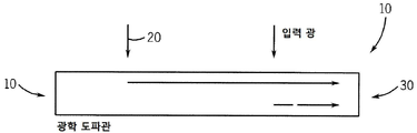
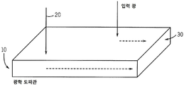
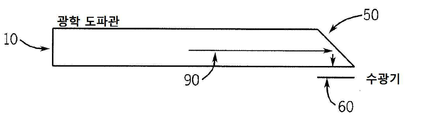
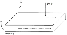
에지 수집기(edge collector) 또는 광학 도파관이 광, 특히, 태양광의 수집과 집광을 위해 사용된다. 에지 수집기 또는 광학 도파관이 이러한 적용예를 위해, 상부 표면으로부터의 광을 수신하고, 집광된 에너지를 장치의 에지로 전달하는 광학 장치로서 형성된다. 도 1a는 광학 도파관(10)의 횡단면의 단순한 개략도를 도시한다. 도 1b는 동일한 광학 도파관(10)의 3D표현이다. Edge collectors or optical waveguides are used for the collection and collection of light, in particular sunlight. An edge collector or optical waveguide is formed for this application as an optical device that receives light from the top surface and delivers the focused energy to the edge of the device. 1A shows a simple schematic view of the cross section of the
실제로, 이들 유형의 광학 도파관(10)은 일반적으로, 미국 특허 7,664,350 및 7,672,549에 기재된 유형을 가진다. 그 밖의 다른 유형의 광학 도파관은 발광 태양 집광기(luminescent solar concentrator) 또는 염료 발광 태양 집광기(dye luminescent solar concentrator)를 포함한다. 도 1c는 전자 유형의 광학 시스템을 보여준다. 입력 광(20)이 개구부를 가로지르는 복수의 집광 유닛(40) 상에 도달하고, 도파관(10)은 모든 유닛으로부터 집광된 광을 수집하고, 상기 광을 도파관(10)의 에지(30)로 전달한다. Indeed, these types of
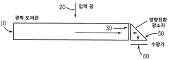
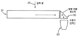
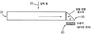
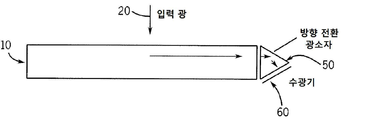
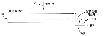
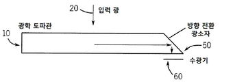
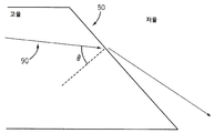
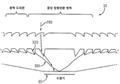
그러나 광(20)을 바람직한 방식으로 방향전환(redirect)하기 위해 에지(30)에 위치하는 광소자(50)의 2차 세트를 갖는 것은 많은 이점을 지닌다. 도 2에서, 광(20)은 도파관(10)의 에지(30)로 전달되고, 도파관(10)의 바닥과 평행하게 위치하는 수광기(60) 쪽으로 대략 90도만큼 방향전환(redirect)된다. 본원에 설명된 발명은 이들 2차 방향전환 광소자(50)를 설계하기 위한 다양한 방법을 기재한다. 본 발명은 광학 도파관(10)을 더 유용하게 만든다. 광학 도파관 집광 시스템에 대한 중요한 산업 기준은 압밀성(compactness), 효율, 집광도(level of concentration), 및 제조역량(manufacturability)을 포함한다. 방향전환에 대한 상이한 방법들이 상이한 방식으로 이들 기준에 영향을 미친다. However, having a secondary set of
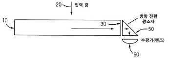
이 광학 도파관(10) 또는 장치에 대한 적용예는 여러 가지이다. 광 에너지가 다양한 수광기로 전달될 수 있다. 도 3a 내지 3d는 집광 또는 확산 광소자, 가령, 렌즈, 복합 포물선형 집광 광소자, 광기전 전지, 또는 열 교환기를 더 포함하는 수광기(60)의 일부 예를 도시하며, 이하에서 더 상세히 기재될 것이다. The application to this
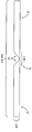
도 1a는 개략적인 광학 도파관의 횡단면도를 도시한다.
도 1b는 개략적인 광학 도파관의 3차원도를 도시한다.
도 1c는 태양 집광에서 사용되는 광학 도파관을 도시한다.
도 2는 광학 시스템의 하나의 실시예를 도시한다.
도 3은 렌즈 수광기를 갖는 하나의 실시예를 도시하고, 도 3b는 CPC 수광기를 갖는 하나의 실시예를 도시하며, 도 3c는 광기전 전지 수광기를 갖는 하나의 실시예를 도시하고, 도 3d는 열 교환기 수광기를 갖는 하나의 실시예를 도시한다.
도 4a는 광학 시스템의 또 다른 실시예를 도시하고, 도 4b는 광학 시스템의 또 다른 실시예를 도시하며, 도 4c는 방향전환 광소자를 포함하는 서로 인접한 복수의 광학 시스템을 도시하며, 도 4d는 방향전환 광소자가 없는 서로 인접한 복수의 광학 시스템을 도시한다.
도 5a는 방향전환 광소자가 도파관으로 일체 구성되는 실시예를 도시하고, 도 5b는 방향전환 광소자가 도파관으로부터 분리되어 있는 실시예를 도시한다.
도 6a-b는 광학 시스템이 중앙 축을 중심으로 거울 대칭되는 하나의 실시예를 도시한다.
도 7a-c는 방향전환 광소자가 집광도의 수준을 수정하는 실시예를 도시한다.
도 8a는 내부 전반사를 이용하는 방향전환 광소자를 도시하고, 도 8b는 부분 굴절을 이용하는 방향전환 광소자를 도시한다.
도 9는 반사를 이용하는 방향전환 광소자를 도시한다.
도 10a는 포물선형 곡선으로 구성된 방향전환 광소자를 도시하고, 도 10b는 부분 굴절을 이용하는 포물선형 곡선을 포함하는 방향전환 광소자를 도시하며, 도 10c는 부분 반사 물빌을 포함하는 포물선형 곡선으로 구성된 방향전환 광소자를 도시하며, 도 10d는 포물선형 곡선과 편평한 면을 포함하는 방향전환 광소자를 도시한다.
도 11a는 TIR 누출을 나타내는 방향전환 광소자의 하나의 실시예를 도시하며, 도 11b는 TIR 누출을 보이는 방향전환 광소자의 또 다른 실시예를 도시하고, 도 11c는 TIR 누출을 보이는 방향전환 광소자의 또 다른 실시예를 도시한다.
도 12a는 방향전환 광소자와 수광기 사이에 공기를 포함하는 방향전환 광소자의 하나의 실시예를 도시하고, 도 12b는 방향전환 광소자와 수광기 사이에 피복 물질을 갖는 방향전환 광소자의 하나의 실시예를 도시한다.
도 13a는 광학 시스템의 하나의 실시예를 도시하며, 도 13b는 비스듬한 도파관을 포함하는 광학 시스템의 하나의 실시예를 도시하고, 도 13c는 반향전환 광소자와 수광기 사이에 피복 물질이 있는 방향전환 광소자의 하나의 실시예를 도시한다.
도 14a-c는 광 파이프 방향전환 광소자의 다양한 실시예를 도시한다.
도 15a는 방향전환 광소자와 수광기 사이에 피복 물질이 있는 방향전환 광소자의 하나의 실시예를 도시하고, 도 15b는 방향전환 광소자와 수광기 사이에 피복 물질과 유리가 있는 방향전환 광소자의 하나의 실시예를 도시한다.
도 16a-e는 광학 시스템의 다양한 실시예를 도시한다.
도 17a는 선형 대칭 광학 시스템을 도시하고, 도 17b는 축 대칭 광학 시스템을 도시하며, 도 17c-f는 축 대칭 광학 시스템 및 이와 연관된 방향전환 광소자의 다양한 실시예를 도시한다.
도 18은 조명 적용예를 위해 구성되는 광학 시스템의 하나의 실시예를 도시한다.1A shows a cross-sectional view of a schematic optical waveguide.
1B shows a three-dimensional view of a schematic optical waveguide.
1C shows an optical waveguide used in solar collection.
2 illustrates one embodiment of an optical system.
FIG. 3 shows one embodiment with a lens receiver, FIG. 3B shows one embodiment with a CPC receiver, FIG. 3C shows one embodiment with a photovoltaic cell receiver, 3D shows one embodiment with a heat exchanger receiver.
4A shows another embodiment of an optical system, FIG. 4B shows another embodiment of an optical system, FIG. 4C shows a plurality of adjacent optical systems including redirecting optical elements, and FIG. 4D A plurality of optical systems adjacent to each other without redirecting optics is shown.
FIG. 5A illustrates an embodiment in which the redirecting optical element is integrally configured with a waveguide, and FIG. 5B illustrates an embodiment in which the redirecting optical element is separated from the waveguide.
6A-B illustrate one embodiment where the optical system is mirror symmetric about a central axis.
7A-C illustrate embodiments in which the redirecting optical device modifies the level of condensing.
FIG. 8A shows the redirecting optical element using total internal reflection, and FIG. 8B shows the redirecting optical element using partial refraction.
9 shows a redirecting optical element using reflection.
FIG. 10A illustrates a redirecting optical device constructed of parabolic curves, FIG. 10B illustrates a redirecting optical device comprising a parabolic curve utilizing partial refraction, and FIG. 10C illustrates a direction consisting of a parabolic curve comprising a partially
FIG. 11A illustrates one embodiment of a redirecting optical device exhibiting a TIR leak, FIG. 11B illustrates another embodiment of a redirecting optical device exhibiting a TIR leak, and FIG. 11C illustrates another embodiment of the redirecting optical device exhibiting a TIR leak. Another embodiment is shown.
FIG. 12A illustrates one embodiment of a redirecting optical element comprising air between the redirecting optical element and the receiver, and FIG. 12B illustrates one of the redirecting optical element having a coating material between the redirecting optical element and the receiver. An example is shown.
FIG. 13A shows one embodiment of an optical system, FIG. 13B shows one embodiment of an optical system that includes an oblique waveguide, and FIG. 13C shows the direction in which the coating material is located between the reverberation optical element and the receiver. One embodiment of the switching optical element is shown.
14A-C illustrate various embodiments of light pipe redirecting optical devices.
FIG. 15A illustrates one embodiment of a redirecting optical element with a coating material between the redirecting optical element and the light receiver, and FIG. 15B illustrates a redirecting optical element with a coating material and glass between the redirecting optical element and the light receiver. One embodiment is shown.
16A-E illustrate various embodiments of optical systems.
17A illustrates a linear symmetric optical system, FIG. 17B illustrates an axial symmetric optical system, and FIGS. 17C-F illustrate various embodiments of an axial symmetric optical system and associated redirecting optical elements.
18 shows one embodiment of an optical system configured for an illumination application.
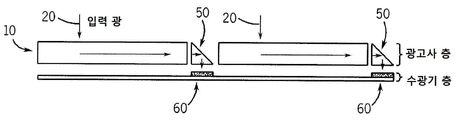
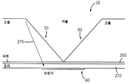
바람직한 실시예에서, 도 4a에 도시된 것처럼, 도파관(10)으로부터의 광이 수집 평면(plane of collection)에 대략 수직인 방향으로 이동한다. 광(20)의 원뿔의 전파의 각도를 변경하기 위해, 방향전환 광소자(50)는 이 광(20)을 수광기(60)로 방향전환시킨다.In a preferred embodiment, as shown in FIG. 4A, light from
바람직한 실시예에서, 도 4b에 도시된 것처럼, 광학 도파관(10)은 도파관(10) 내 자신의 전파 각도에 실질적으로 수직인 방향으로 광(20)을 방향전환시킨다. 이는 도 4c에 나타난 것처럼 수광기(60)가 수집 평면에 평행하게 놓이는 것을 가능하게 한다. 도 4d는 광학 도파관(10)이 자신과 연관된 방향전환 광소자를 갖지 않은 경우, 도파관(10)과 수광기(60)가 어떻게 서로 간섭을 일으키는지를 나타낸다. "광소자 층(optics layer)"(방향전환 광소자(50)) 및 "수광기 층"(수광기(60))이 쉽게 조립 및 짝결합(mate)될 수 있는 수평 슬래브(slab) 섹션을 형성한다. 2개의 층은 견고하고 내구성 있는 박판 구성을 형성할 수 있다. 수광기(60)들 간의 연결이 더 쉽게 만들어질 수 있는데, 예를 들어, 광기전 전지 수광기들 간의 전기적 상호 연결이 있다. 수광기(60)(가령, 광기전 전지)가 승온됨에 따라, 개별 수광기 층을 갖는 것이 후면 열 싱크(heat sink)로부터의 더 효율적인 열 전달을 가능하게 한다. In a preferred embodiment, as shown in FIG. 4B, the
이하의 섹션 각각은 방향전환 광소자(50)에 의해 해결되는 특정 문제와 상기 문제를 해결하는 일부 선호되는 방법의 개요를 서술한다.Each of the sections below describe an overview of the specific problem solved by the redirecting
1. 동일 부분 또는 별개 부분으로서의 방향전환기 1. Redirector as same or separate part
도 5a에 도시된 것처럼, 방향전환 광소자(50)는 도파관(10)과 동일한 제조 부분의 특징이도록 구성될 수 있다. 도 5b에 도시된 것처럼, 방향전환 광소자는 또 다른 실시예에서 별개 부분일 수도 있다.As shown in FIG. 5A, the redirecting
동일 부분으로 만들어지는 것은 도파관(10)에 대해 이점을 갖는데, 즉, 제조 단계가 더 적고, 부분들 간 정렬이 필요 없으며, 계면들 사이에 어떠한 소실도 없기 때문에 효율이 더 클 가능성이 있다.Being made in equal parts has an advantage for the
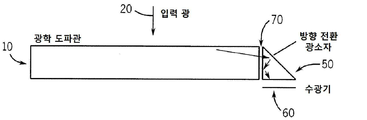
도파관(10)과 방향전환 광소자(60)의 구성요소에 대해 개별 부분으로 만들어지는 것은 광 집광도의 수준을 보존하거나 향상시키는 데 도움이 될 수 있다. 계면(70)은 내부 전반사(TIR: totally internally reflecting) 표면으로서 기능할 수 있고, 따라서 도파관(10) 내부에 광(20)을 더 잘 유지할 수 있다.Being made into separate parts for the components of
2. 거울 이미지 2. mirror image
도 6a는 앞서 언급된 것과 같은 광학 도파관(10)과 방향전환 광소자(50)를 도시하는데, 여기서 입력 광(20)의 수집 영역과 광소자 구성요소의 높이가 나타나 있다. FIG. 6A shows the
도 6b에서, 도파관(10) 광소자, 방향전환 광소자(50), 및 수광기(60)의 조합이 중앙 축을 중심으로 거울 대칭된다. 그 후, 수광기(60)는 하나의 연속하는 부분으로서 구성될 수 있다. 따라서 광을 단일 수광기(60)로 전달하는 수집 영역은 두 배가 되고, 총 구성의 높이는 변하지 않는다. 따라서 구성은 수광기(60)의 주어진 면적에 대해 2배 더 압밀(compact)하다.In FIG. 6B, the combination of
덧붙여, 전체 거울 대칭되는 도파관 및 방향전환 조합이 하나의 부분으로 제조됨으로써, 제조를 단순화시킬 수 있다.In addition, the entire mirror symmetric waveguide and redirection combination can be manufactured in one piece, thereby simplifying manufacturing.
3. 2차 집광 3. Secondary condensing
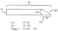
광학 도파관(10)은 수집 면적 A1을 에지의 영역 A2로 나눈 값으로 정의되는 도 7a의 실시예에서 C1으로 나타나는 바와 같은 특정한 집광도 수준을 전달한다. 방향전환 광소자(50)는 이러한 집광도 수준으로 광(20)을 수신하고, 수광기(60)로 전다로디면 집광도 수준을 변경할 수 있다.
방향전환 광소자(50)에 의해 야기되는 2차 집광(secondary concentration)은 C2로 나타내어지고 A2, 즉, 방향전환 광소자(50)에 대한 입력 면적, 및 A3, 즉 방향전환 광소자(50)에 대한 출력 면적의 비로 정의된다. 최종 집광도 수준은 Cfinal로 나타내어지고, A1/A3으로 정의된다. The secondary concentration caused by the redirecting
도 7a에서, 방향전환 광소자(50)는 광학 도파관(10)으로부터의 집광도의 수준을 증가시킨다. 따라서 Cfinal은 C1보다 크다. 가령, 태양 패널(solar panel)의 비용을 감소시키기 위해 광기전 전지 재료의 면적을 감소시킬 때와 같이, 집광도 팩터(concentration factor)가 핵심 파라미터인 경우, 방향전환 광소자(50)로부터의 2차 집광이 유익할 수 있다. In FIG. 7A, the redirecting
도 7b의 실시예에서, 방향전환 광소자(50)는 광학 도파관(10)으로부터의 집광도의 수준을 감소시킨다(Cfinal < C1). 도 7b의 특정 실시예에서, 단순한 편평한 면(flat facet)(80)은 광학 도파관(10) 또는 에지 수집기의 수평 바닥에 대해 대략 완만한 각(shallow angle)으로 배치되고, 집광도의 감소를 전달할 수 있다. 도 7c에서, 이 실시예는 추가 예시를 제공한다. 광학 도파관(10)이 주목할만한 집광도 수준을 전달했을지라도, 방향전환 광소자(80)는 최종 집광도 팩터를 약 2x까지로 감소시켰다. 이는, 예를 들어, 전체 광학 시스템은 매우 압밀하게 유지하면서, 태양 전지 물질을 2배만큼 감소시키고, 대면적의 연속 태양 전지를 갖는 것이 바람직할 때, 이로울 수 있다. In the embodiment of FIG. 7B, the redirecting
4. 내부 전반사의 한계 4. Limitations of Internal Total Reflection
방향전환되도록 광(20)을 반사시키기 위해 내부 전반사(TIR)가 사용될 수 있다. 반사성 코팅은 자신에게 도달한 에너지의 일부를 흡수할 것인데 반해, 이는 거의 무소실이기 때문에 반사성 코팅보다 뛰어나다. 또한, 반사성 코팅의 추가적인 제조 단계 및 재료 비용을 제거하기 때문에, 더 저렴하다.Total internal reflection (TIR) can be used to reflect the light 20 to be redirected. Reflective coatings will absorb some of the energy that reaches them, while they are almost lossless and outperform reflective coatings. It is also cheaper because it eliminates additional manufacturing steps and material costs of the reflective coating.
그러나 내부 전반사는 광소자 및 이를 둘러싸는 물질의 굴절률에 의해 형성되는 임계각(critical angle)보다 큰 입사각을 제공하는 광선에 대해서만 발생한다. However, total internal reflection occurs only for light rays that provide an angle of incidence greater than the critical angle formed by the refractive index of the optical element and the material surrounding it.
도 8a의 실시예에서, TIR 한계에서의 편평한 방향전환 광소자(50)가 도시된다. 광선(90)과 계면의 법선 사이에 형성된 각 세타(theta)가 임계각보다 간신히 크다. 도 14a-c는 광선(90)의 각이 임계각보다 작을 때 어떤 일이 발생하는지를 보여준다(광선이 방향전환 광소자(50) 표면을 통해 굴절되고 수광기(60)로 전달되지 않는다). 따라서 TIR을 이용하기 위한 요건이 효율을 보존하면서 추가적인 2차 집광이 발생할 수 있는 횟수에 대해 제약을 둔다.In the embodiment of FIG. 8A, a flat redirecting
5. 반사성 코팅 5. Reflective coating
또 다른 실시예에서, TIR 한계가 허용하는 것보다 더 광을 집광시키기 위해 반사성 코팅이 채용될 수 있다. 도 9는 이 실시예를 도시한다. 이 경우, 입사각은, 광(90)이 실질적으로 소실된 도 8b의 것과 유사하다. 여기서, 대신, 광선(90)은 수광기(60) 쪽으로 반사된다. 따라서 반사체(100)에 의해 방향전환 광소자(50)는 광학 도파관(10)에 대해 더 가파른 경사를 제공하는 형태를 가지며, 이는 계면을 통과하는 광선 소실 없이 2차 집광을 향상시킬 수 있다. (그러나 본원의 섹션 4에서 기재된 것처럼, 효율에 대한 트레이드오프(tradeoff)는 반사체가 자신에게 도달하는 에너지의 일부를 흡수한다는 것이다.)In another embodiment, a reflective coating can be employed to focus light more than the TIR limit allows. 9 shows this embodiment. In this case, the angle of incidence is similar to that of FIG. 8B where light 90 is substantially lost. Here, instead, the
6. 곡선형 방향전환 광소자 6. Curved redirection optical device
곡선형 섹션, 가령, 도 10a의 포물선형 섹션(110)은 2차 집광을 전달할 때 편평한 표면보다 더 효율적일 수 있다. 곡선, 가령, 포물선은 포커싱 광학 표면(focusing optical surface)이고, 따라서 광학 도파관(10)으로부터 광 원뿔을 취하고, 수광기(60)로 전달되는 2차 수준의 집광을 수행할 수 있다. Curved sections, such as
그러나 도 10b에 도시된 것처럼, 곡선(110)은 내부 전반사를 위해 입사각을 초과하는 광(90)의 입사각을 갖기에 충분히 가팔라질 수 있다. 두 가지 해결책이 가능하다. 첫째, 도 10c에 도시된 것처럼, 반사성 코팅(120)이, 다른 경우라면 광 누출(leaking out)을 보였을 곡선(110)의 섹션에 적용될 수 있다. 둘째, 방향전환 광소자를 따라 TIR이 항상 이뤄지도록, 포물선(110)이 TIR 한계에서 절단될 수 있고, 편평한 면(130)이 곡선의 단부와 동일한 각도로 사용될 수 있다. 이 특징은 도 10d에서 나타난다. However, as shown in FIG. 10B, the
7. TIR "누출" 7. TIR "leak"
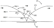
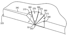
또 다른 실시예에서, 광학 도파관(10)과 방향전환 광소자(60)가 거울 대칭될 때, 도 11a에 도시된 것처럼, 방향전환 광소자(50) 표면으로부터의 광(140)의 약간의 누출은, 대향하는 방향전환 표면에 의해 수집되고 수광기(60)로 전달되기 때문에, 허용될 수 있다. 이는, 방향전환 광소자(50) 표면이 가파른 각으로 배치될 수 있고, 따라서 수광기(60)의 필요한 면적을 축소시킬 수 있기 때문에, 얻어질 수 있는 2차 집광을 증가시킬 수 있다. In another embodiment, when the
또 다른 실시예에서, 이러한 효과를 이용하기 위해 면(160)들의 연립이 가능하며, 이때, 도 11b에 도시된 것처럼, 면(160)들 중 더 가파른 면일수록 바닥 표면에 더 가까이 위치한다. 각각의 면(160)은, 면에 입사하는 광선의 각의 범위가 주어질 때 집광도와 효율 모두를 최대화하기 위해 적절한 각으로 배치될 수 있다. 또는, 도 11c의 실시예에 도시된 것처럼, 면(160)들의 연립에 가까운 곡선형 표면(170)이 동일한 것을 달성하기 위해 적용될 수 있다. 또한 도 11c에 도시된 것처럼, 방향전환 광소자(50)는 복수의 곡선, 가령, 포물선 섹션(170)과 호(180)로 구성될 수 있다. In another embodiment, coalescing of the
8. 바닥 상의 피복재 8. Cladding on the floor
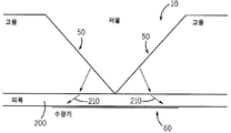
또 다른 실시예에서, 광소자(50)의 바닥과 수광기(60)의 상부 사이에 공기(190)가 사용되는 경우, 도 12a에 도시된 것처럼, 방향전환 광소자(50)를 빠져나가는 광(210)이 원뿔각을 증가시키도록 회절할 것이다.In another embodiment, when air 190 is used between the bottom of the
도 12b에 도시된 것처럼, 피복 물질(200)이 도파관-방향전환 광소자 구성의 바닥에 도포될 수 있다. 피복(200)은 방향전환 광소자(50)의 매질보다 낮은 굴절률을 가진다. 이로 인해서, 광학 시스템의 바닥으로부터의 굴절이 완화되기 때문에(광선(210)이 광소자에서 또 다른 물질로의 이동할 때보다 광소자에서 가능한 최저 굴절률을 갖는 공기로 이동할 때 더 많이 굴절될 것이기 때문에), 수광기(60)에서의 광(210)의 원뿔이 더 좁아진다. 방향전환 광소자(50)로부터의 원뿔각을 완화시키는 것이 전체 광학 시스템에 의해 얻어지는 집광도의 수준을 보존하는 데 도움이 될 수 있다. As shown in FIG. 12B, a
또한 피복은 효율 이점을 제공할 것이다. 프레넬 반사(Fresnel reflection)가 상이한 굴절률들의 계면에서 발생하고, 여기서 굴절률의 차이가 클수록 더 많이 소실된다. 광소자와 수광기(160) 사이에 공기를 갖는 것이 가장 큰 프레넬 반사 소실을 초래할 것이다. The coating will also provide an efficiency advantage. Fresnel reflection occurs at the interface of different refractive indices, where the greater the difference in refractive index, the more it is lost. Having air between the optical device and the
또한 피복은 구조적 이점과 신뢰성 이점을 제공할 수 있다. 피복은 환경 보호가 필요한 민감한 물질, 가령, 광기전 전지를 캡슐화할 수 있다. 또한 피복은, 예를 들어, 온도가 증가하는 환경에서 상이한 팽창 속도로 인한 광소자와 수광기(160) 사이의 응력을 분해할 수 있다.The coating can also provide structural and reliability advantages. The coating can encapsulate sensitive materials that require environmental protection, such as photovoltaic cells. The sheath can also resolve stresses between the optical element and the
9. 비스듬한 도광관(angled light guide) 9. Angled light guide
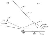
대안적 실시예에서, 도 13a에 도시된 것처럼, 도파관(10)에서 광 원뿔의 전파 방향은 입력 광에 정확히 수직일 필요는 없다. 일 변형예에서 도 13b에 도시된 것처럼, 도파관(220)은 수평선에 대해 비스듬하게 구성될 수 있다.In an alternative embodiment, as shown in FIG. 13A, the propagation direction of the light cone in
비스듬한 형태의 도파관(10)은 TIR 한계에서 더 우수한 2차 집광이 유지될 수 있게 하기 때문에 방향전환 광소자(50)에 대해 바람직하다. 이유는 광이 더 작은 필요한 방향전환 각을 갖기 때문이다. 도 13b는 이러한 이점을 나타낸다 - 광선(90)은 도 13a에 나타난 것보다 더 큰 각도에 걸쳐 내부 전반사를 통해 반사될 수 있다.The obliquely shaped
도 13c는 비스듬한 도파관(220)이 바닥 상의 피복(200)과 결합될 때 필요한 면(230)의 각의 변경을 도시한다. 초점 영역(25)으로부터 반사되는 극한 광선(extreme ray)을 다루기 위해, 최종 면(24)("면 2")은 이전 면(23)("면 1")보다 완만한 각으로 있을 필요가 있으며, 그렇지 않은 경우, 초점 영역으로부터 반사되는 광선(235)이 면 2을 통해 굴절하여 위쪽으로 빠져나갈 것이다. FIG. 13C shows a change in the angle of the
10. 방향전환 광 파이프 10. turn light pipe
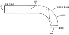
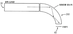
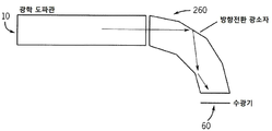
대안적 실시예는 더 우수한 2차 집광을 얻기 위해 종횡비를 증가시키는 것과 관련된다. 도 14a는 광(265)을 방향전환시키기 위한 곡선형 광 파이프(260)의 사용을 도시한다. 광학 도파관(10)-방향전환 광소자(260)의 종횡비는 상당히 더 크게 만들어진다. 도 14b는 방향전환 광소자의 곡선형 표면을 맞춤 구성(tailoring)하거나 파이프 특징부 유형의 방향전환 광소자(260)를 차츰 가늘어지게 함으로써, 2차 집광을 이루는 것을 제외하고 동일한 구성을 도시한다. 도 14c는 곡선형 섹션 대신 방향 전환 광소자(260)에 대한 편평한 면을 가진다는 것을 제외하고 유사한 접근법을 도시한다. Alternative embodiments relate to increasing the aspect ratio to obtain better secondary condensing. 14A illustrates the use of curved
지금까지 설명한 바와 같이, 파이프 특징부(260)는, 광학 도파관(10)에 의해 제공되는 집광도의 수준을 보존하고, 광 원뿔을 수광기(60)를 직접 대면하도록 배향하며, 2차 집광도의 최대 수준을 얻을 수 있기 때문에, 원칙적으로 방향전환 광소자보다 더 우수한 2차 집광을 달성할 수 있다. 이전의 방향전환 광소자는 최대 허용 가능한 수준의 2차 집광도를 얻는 것을 방해하는 내부 전반사 제약에 직면했다. As described so far, the
그러나 이전의 방향전환 광소자(260)는 광학 도파관의 압밀성(compactness)을 유지한다. 따라서 다음의 트레이드오프가 나타난다:However, the previous redirecting
ㆍ 최고 압밀성과 최고 효율을 달성하지만 최고 집광도는 달성하지 않는 TIR 비-파이프 접근법TIR non-pipe approach that achieves the highest compactness and the highest efficiency but no peak condensation
ㆍ 최고 압밀성과 최고 집광도를 달성하지만 최고 효율은 달성하지 않는 반사체 비-파이프 접근법Reflector non-pipe approach that achieves the highest compactness and the highest light collection but does not achieve the highest efficiency
ㆍ 최고 집광도와 최고 효율은 달성하지만 최고 압밀성은 달성하지 않는 TIR 파이프 접근법TIR pipe approach that achieves the highest light collection and highest efficiency but does not achieve the highest compaction
11. 바닥 유리 11.bottom glass
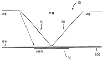
또 다른 실시예는 우수한 집광도를 얻기 위해 종횡비를 약간 증가시킨다. 도 15a는 이미 설명된 설계를 도시하며, 여기서, 방향전환 광소자(50)가 피복 층(200)을 가진다. 도 15b는 유리(270) 같은 광학 재료의 시트가 도파관-방향전환 광소자 구조의 바닥에 배치되는 방식을 도시한다. 추가 높이에 의해, 광(275)이 더 긴 이동 거리를 갖기 때문에 더 우수한 2차 집광이 가능해지며, 에지 광선의 각은 이동 거리가 길수록 최종 초점 영역을 축소시키도록 정해진다.Another embodiment slightly increases the aspect ratio to obtain good light condensation. 15A shows the design already described, where the redirecting
또한 바닥 유리(270)는, 광학 구성요소 내 공극(void)을 초래할 수 있는 먼지 및 습기로부터, 그리고 열 및 그 밖의 다른 팽창 및 수축으로 인한 기계적 응력으로부터 수광기(60)(가령, 태양 전지)를 보호하는 기계적 및 환경적 장벽으로서 기능할 수 있다.The
12. 중앙 방향전환을 위한 지지 광소자 12. Supporting optical element for central turning
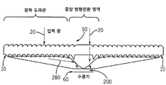
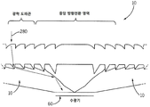
전체 도파관-방향전환 광소자 구조물이 상부 표면으로부터 광(20)을 효율적으로 수집하도록 설계되기 때문에, 구조물의 (방향전환 광소자 위의) 중앙 영역 상에 도달하는 광(20)도 최적의 효율을 위해 수집되어야 한다.Since the entire waveguide-turning optical device structure is designed to efficiently collect light 20 from the top surface, the light 20 arriving on the central region (on the redirecting optical device) of the structure also provides optimum efficiency. Should be collected.
도 16a는 중앙 방향전환(central redirection)을 위한 지지 광소자를 포함하는 완전한 도파관(10)-방향전환 광소자(50) 조합을 갖는 하나의 실시예를 도시한다. 광학 도파관(10)의 전체 전면 표면에 도달하는 입력 광(20)이 수광기(60)로 전달되도록 설계된다.FIG. 16A shows one embodiment with a complete waveguide 10-redirecting
도 16b는 중앙 방향전환 영역의 확대도를 나타낸다. 앞서 언급된 바와 같은 수광기(60)로의 경로와 함께, 광학 도파관(10)으로부터의 광선(280)이 도시된다.16B shows an enlarged view of the center redirecting area. Along with the path to the
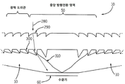
문제는 중앙 방향전환(50) 영역으로부터의 광선(20)이 어떻게 수광기(60)로 나아갈 수 있냐는 것이다. 세 가지 접근법이 가능하며, 조합되는 것이 바람직하다. 첫째, 방향전환 광소자(50) 상에 서로 다른 비스듬한 표면을 수용하도록, 광학 도파관(10)의 섹션의 설계가 수정될 수 있다. 도 16c에서, 수광기(60) 쪽으로의 방향전환 광소자 표면(310)의 기울어짐을 수용하기 위해, 광선(280)이 이동할 때 통과하는 시스템은 더 큰 렌즈(290)와 면(300) 특징부를 가진다. 따라서 광선(280)은 앞서 설명된 다른 실시예로부터 광학 도파관(10) 시스템 내 광선(20)과 상이한 경로를 통해 이동한다.The problem is how the
둘째, 광(280)을 방향전환 광소자(50) 상의 적절한 위치로 지향시켜, 광이 수광기(60)로 전달되도록, 상부 요소에 특징부들이 배치될 수 있다. 도 16d에서, 광선이 수광기(60) 바로 위의 영역에서 방향전환 광소자 표면(310)과 교차하도록 상부 요소의 바닥 상의 톱니 특징부(320)가 광선(280)을 방향전환시킨다. 이러한 톱니 특징부(320)가 없는 경우, 광선(280)이 수광기(60)에 충돌하지 않아서 효율이 제한되거나, 수광기(60)가 광선(280)을 수용하기에 더 넓어서 집광을 제한할 것이다. Second, features may be placed on the upper element such that
셋째, 광학 구성요소의 시스템의 중심에 충분히 가까이 있는 광선은 방향 변화 없이 통과될 수 있다. 이들 광선은 방향전환 표면 광소자(310)에 충돌할 때 약간의 굴절을 겪지만, 이들은 시스템의 중심에 충분히 가까워서, 수광기(60) 상에 결국 도달함이 보장된다. Third, light rays sufficiently close to the center of the system of optical components can pass through without changing direction. These rays undergo some refraction when impinging on the redirecting
앞서의 두 번째 및 세 번째 선택사항은 전체 방향전환 광소자(310)가 반사체 없이 구성될 것을 요구한다 - 즉, 순수 TIR이 사용된다. 방향전환 광소자(310) 상의 반사성 코팅은 중앙 방향전환 영역으로부터의 들어오는 광선을 차단할 것이며, 이는 효율을 제한한다. The second and third options above require the entire redirecting
도 16a-e는 하나의 바람직한 실시예에서 이전 섹션들에서 언급된 다수의 요소들을 조합한다.16A-E combine a number of elements mentioned in the previous sections in one preferred embodiment.
ㆍ 섹션 1에서 단순화된 제조를 위해 방향전환 광소자(310)는 광학 도파관(10)과 하나의 부분으로서 만들어진다. The redirecting
ㆍ 섹션 2에서 광학 도파관(10)-방향전환 광소자(50)는 중앙 축을 중심으로 거울 대칭되어, 전체 장치의 수집 영역 및 압밀성이 증가한다.In
ㆍ 섹션 3에서 Cfinal > C1이도록 광학 도파관(10)은 2차 집광을 이룸으로써, 수광기(60) 영역이 감소되고, 따라서 수광기 비용이 감소된다.The
ㆍ 섹션 4에서 방향전환 광소자(310)는 효율을 최대화하기 위해 내부 전반사를 이용한다. In section 4 the redirecting
ㆍ 섹션 6에서 2차 집광도를 증가시키기 위해 방향전환 광소자(310)는 포물선형 곡선을 채용하고, 그 후, TIR 한계에 도달할 때 편평한 면으로 곡선을 절단(truncate)한다. (몇 개의 편평한 면에 의해 포물선형 곡선이 근사되어, 비교될만한 결과를 얻을 수 있다) To increase the secondary light intensity in section 6 the redirecting
ㆍ 섹션 7에서 방향전환 광소자(310)는 "TIR 누출"을 가능하게 한다 - 일부 광선이 임계각을 위반하여, 거울 이미지 표면 너머로 굴절될 수 있지만, 그럼에도, 여기서 광선은 수광기(60)에 의해 수집된다. 이로 인해, 방향전환 표면(310)은 추가적인 2차 집광을 가능하게 하는 더 가파른 각을 가질 수 있다.Redirecting
ㆍ 섹션 8에서 방향전환 광소자와 수광기 사이에서 피복(200)이 사용되어, 집광, 효율, 구조적 지지, 및 신뢰성을 향상시킬 수 있다.In section 8 a
ㆍ 섹션 9에서 광학 도파관(10)은 비스듬한 도파관(angled waveguide)이다. - 즉, 도파관(10)은 입력 광(20)에 완벽하게 수직이 아니다. 이로 인해, 방향전환 광소자(310)는 더 가파른 각을 가질 수 있고, 이로써 얻어질 수 있는 2차 집광도가 증가한다.The
ㆍ 섹션 12에서, 지지 광소자(290, 300, 320)가 방향전환 광소자(310) 위의 광학 도파관(10)의 중앙 방향전환 영역에서 구성된다. 이들 지지 광소자는 중앙 영역에 입사하는 광이 방향전환 광소자(310)를 통해 수광기(60)로 전달됨을 보장하여, 효율 및 집광도를 최대화한다.In section 12, the supporting
앞서 언급된 바와 같이, 방향전환 광소자(50)는 포물선형 표면, 타원형 표면, 쌍곡포물선형 표면, 호(arc), 편평한 반사성 표면, 맞춤 구성된 형태(tailored shape)의 반사성 표면, 내부 전반사성 표면, 구성 포물선형 집광기 광소자, 광 파이프, 및 굴절성 구성요소의 임의의 조합을 포함할 수 있다.As mentioned above, the redirecting
이전 섹션들은 방향전환 광소자(50)의 다양한 실시예를 설계하기 위한 방법을 기재했다. 이하에서, 방향전환 광소자(50)에 대한 두 가지 대안적 구현예가 기재된다. 이전 요소들에 대한 모든 기재가 이하의 두 구현예에 적용된다. The previous sections described a method for designing various embodiments of the redirecting
선형 대칭 광소자 대 축 대칭 광소자Linear Symmetric Optical Devices vs. Axial Symmetric Optical Devices
설계도가 횡단면으로 나타나기 때문에 광학 구성요소는 도 17a에 도시된 것처럼 선형 압출물로 렌더링되거나, 도 17b에 도시된 것처럼 회전 압출물로 렌더링될 수 있다. 본원에 기재된 모든 요소들은 어느 압출물에도 적용될 수 있다. Because the schematic is shown in cross section, the optical component can be rendered as a linear extrudate as shown in FIG. 17A or as a rotating extrudate as shown in FIG. 17B. All of the elements described herein can be applied to any extrudate.
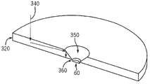
그러나 회전 압출물 내 축 대칭 광소자는 추가로 해결될 과제를 가진다. 도 17c는 익숙한 케이스를 보여준다 - 광학 도파관(320)으로부터의 광선(20)이 중앙 수광기(60)를 향해 하향으로 방향전환된다. 그러나 회전 압출물에서, 광선(20)은 설계된대로 방향전환되도록 방향 전환 광소자(330)에 충돌하기 위해, 디스크의 반지름과 완벽하게 정렬되어야 한다(방향전환 광소자(330)의 팁(tip)이 회전 압출물 내 한 점에 도달한다). 도 17d에서, 중심에서 약간 벗어난 광선(340)은 방향전환 광소자(330)에 빗맞고, 수광기(60)에 도달하지 않는다. However, axially symmetric optical elements in rotating extrudate have further challenges. 17C shows a familiar case-the
도 17e에서, 회전 축을 방향전환 광소자(330)의 팁으로부터 멀리 이동시킴으로써 이는 개선된다. 따라서 광선(340)은 한 점이 아니라 벽(350)을 대면한다. 효율을 최대화하기 위해 실질적으로 모든 도파관 광(20)이 포착되도록, 광소자(360)의 팁으로부터 회전 축까지의 거리는 조정될 수 있다. 단점은 동일한 횡단면 설계의 선형 압출물에 비해 2차 집광이 약하다는 것이다.In FIG. 17E, this is improved by moving the axis of rotation away from the tip of the redirecting
도 17f는 문제를 해결하기 위한 또 다른 방식에서의 하나의 실시예를 도시한다. 방향전환 광소자 팁(360)은 회전 축으로서 취급된다. 그러나 방향전환 영역(50)은 축을 중심으로 주기적인 간격으로 나누는 수직 슬릿(slit)(380)을 가진다. 이들 슬릿(380)은 공기 또는 저율 피복 물질로 충전될 수 있거나, 방향전환 영역(50)의 벽이 반사체에 의해 코팅될 수 있다. 중심에서 벗어난 광선(340)은 벽(380)들 중 하나에 충돌할 것이고, 중심 쪽으로 다시 반사될 것이다. "도광 벽(guide wall)"의 하나 또는 복수의 반사 후, 광선(340)은 방향전환 광소자(370)의 방향전환 표면과 마지막으로 상호작용하고 수광기(60) 쪽으로 방향전환될 것이다. 이 접근법은 동일한 횡단면도의 선형 압출물에서 얻어질 수 있는 2차 집광을 보존할 수 있다. 반사성 코팅이 사용되지 않는 경우, 즉, 내부 전반사가 유일한 수단인 경우, 이 접근법은 효율도 최대화한다. 17F shows one embodiment in another way to solve the problem. The redirecting
광 확산 또는 조명을 위한 역방향 광학 경로Reverse optical path for light diffusion or illumination
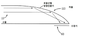
또 다른 실시예에서, 지금까지 본원에 기재된 광소자는 광 수집 및 집광을 위한 것이었다. 그러나 역방향의 광학 시스템은 효과적인 광 확산기(diffuser)이다.In yet another embodiment, the optical devices described so far have been for light collection and collection. However, the reverse optical system is an effective light diffuser.
도 18에서, 광(400)이, 지금까지 수광기(60)(바닥의 중심 영역)였던 광원(290)으로부터 장치로 들어간다. 광(400)은 방향전환 광소자(50)를 통해 광학 도파관(10) 내부로 방향전환되고, 광학 도파관(10)은 실질적으로 수평방향으로 이동하는 광을 취하고, 광을 확산시켜, 도파관(10)의 표면에 실질적으로 수직인 광선(410)을 출력한다. 도파관(10)의 상부 표면은, 임의의 범위의 각으로 광을 발산하기 위해 렌즈 또는 그 밖의 다른 광학 요소에 의해 조정될 수 있다. 따라서 장치는 매우 압밀하고 효율적인 광 확산기이다. 적용예는 LED 광소자, 루미네어(luminaire), 스포트라이트, 및 자동차용 전조등 및 미등을 포함한다.In FIG. 18, light 400 enters the apparatus from
본 발명의 실시예에 대한 상기의 기재는 예시와 설명 목적으로 제시되었다. 개시된 정확한 형태로 본 발명을 배제하거나 제한하려는 의도가 아니며, 발명의 범위 내에서 본 발명의 실시를 통해 획득될 수 있는 수정과 변형이 가능하다. 본 발명의 원리 및 실제 적용예를 설명하기 위해 실시예가 선택 및 기재되었고, 특정 용도에 적합한 다양한 실시예 및 다양한 수정예로 해당 분야의 통상의 기술자가 본 발명을 실시할 수 있다.
The foregoing description of the embodiments of the invention has been presented for purposes of illustration and description. It is not intended to be exhaustive or to limit the invention to the precise form disclosed, and modifications and variations are possible that may be acquired through practice of the invention within the scope of the invention. Embodiments have been selected and described in order to explain the principles and practical applications of the invention, and various embodiments and various modifications suitable for a particular use can be practiced by those skilled in the art.
Claims (19)
입력 광을 수집하고 집광시키기 위한 광학 도파관,
집광된 광을 수신하기 위한 수광기,
수광기 위에 위치하는 중앙 방향전환 영역(central redirecting region)
을 포함하며, 광학 도파관의 중앙 방향전환 영역은 광을 광학 도파관에서 수광기 쪽으로 방향전환시키기 위한 방향전환 광소자를 포함하며, 상기 방향전환 광소자는 중앙 축을 중심으로 거울 대칭되며, TIR 누출(TIR leaking)을 가능하게 하는 비스듬한 표면(angled surface)을 갖는, 광학 집광 시스템.As an optical condensing system,
Optical waveguides for collecting and condensing input light,
A light receiver for receiving the collected light,
Central redirecting region located above the receiver
Wherein the central redirecting region of the optical waveguide comprises a redirecting optic for redirecting light from the optical waveguide toward the receiver, the redirecting optic being mirror symmetric about a central axis and having a TIR leaking. An optical condensing system having an angled surface that facilitates the use.
중앙 축으로부터 축방향으로 뻗어 있는 광학 도파관,
광학 도파관 아래에 위치하고 중앙 축으로부터 뻗어 있는 중앙 수광기
를 포함하되, 광학 도파관은 중앙 축을 중심으로 그리고 중앙 수광기 위에 위치하는 방향전환 영역을 갖고, 상기 방향전환 영역은 광을 중앙 수광기 쪽으로 방향전환시키기 위한 복수의 특징부를 포함하는, 광학 시스템.As an optical system,
An optical waveguide extending axially from the central axis,
Central receiver located under the optical waveguide and extending from the central axis
Wherein the optical waveguide has a redirecting region located about the central axis and above the central receiver, the redirecting region comprising a plurality of features for redirecting light towards the central receiver.
Applications Claiming Priority (5)
| Application Number | Priority Date | Filing Date | Title |
|---|---|---|---|
| US40777210P | 2010-10-28 | 2010-10-28 | |
| US61/407,772 | 2010-10-28 | ||
| US12/939,348 | 2010-11-04 | ||
| US12/939,348 US8412010B2 (en) | 2007-09-10 | 2010-11-04 | Compact optics for concentration and illumination systems |
| PCT/US2011/057876 WO2012058304A2 (en) | 2010-10-28 | 2011-10-26 | Redirecting optics for concentration and illumination systems |
Publications (1)
| Publication Number | Publication Date |
|---|---|
| KR20130130707A true KR20130130707A (en) | 2013-12-02 |
Family
ID=45994720
Family Applications (1)
| Application Number | Title | Priority Date | Filing Date |
|---|---|---|---|
| KR1020137010535A KR20130130707A (en) | 2010-10-28 | 2011-10-26 | Redirecting optics for concentration and illumination systems |
Country Status (8)
| Country | Link |
|---|---|
| US (2) | US8705914B2 (en) |
| EP (1) | EP2633349A4 (en) |
| JP (1) | JP5944398B2 (en) |
| KR (1) | KR20130130707A (en) |
| CN (1) | CN103238091A (en) |
| AU (1) | AU2011319939A1 (en) |
| CA (1) | CA2815671C (en) |
| WO (1) | WO2012058304A2 (en) |
Families Citing this family (18)
| Publication number | Priority date | Publication date | Assignee | Title |
|---|---|---|---|---|
| AU2010246958B2 (en) * | 2009-05-14 | 2015-03-19 | Sunboost Ltd. | Light collection system and method |
| TWI538239B (en) * | 2011-02-14 | 2016-06-11 | Light collection device and its light collection method | |
| EP2654317B1 (en) * | 2012-04-17 | 2014-06-18 | Siemens Aktiengesellschaft | Input/output component with display element |
| JP2015216138A (en) * | 2012-09-10 | 2015-12-03 | シャープ株式会社 | Solar cell module and photovoltaic power generation device |
| KR200482441Y1 (en) | 2012-12-27 | 2017-01-24 | 젠텍스 코포레이션 | Light system |
| US9595627B2 (en) | 2013-03-15 | 2017-03-14 | John Paul Morgan | Photovoltaic panel |
| US9960303B2 (en) | 2013-03-15 | 2018-05-01 | Morgan Solar Inc. | Sunlight concentrating and harvesting device |
| CN105051454B (en) | 2013-03-15 | 2019-06-18 | 摩根阳光公司 | Tabula rasa, the tabula rasa with the optical module for improving interface and with improved fabrication tolerance |
| US9714756B2 (en) | 2013-03-15 | 2017-07-25 | Morgan Solar Inc. | Illumination device |
| US9985156B2 (en) | 2013-11-01 | 2018-05-29 | UNIVERSITé LAVAL | Optical concentrator/diffuser using graded index waveguide |
| JP2015099336A (en) * | 2013-11-20 | 2015-05-28 | 株式会社東芝 | Optical element and optical device |
| AU2014370354B2 (en) * | 2013-12-23 | 2018-10-25 | Alcon Inc. | Power source for an accommodating intraocular lens |
| TWI552516B (en) * | 2015-01-29 | 2016-10-01 | 國立交通大學 | Sunlight manipulating device |
| US10473904B2 (en) * | 2015-01-29 | 2019-11-12 | National Chiao Tung University | Sunlight modulation device with divergent reflection of converged sunlight for solar energy utilization |
| ES1221605Y (en) | 2016-11-03 | 2019-02-28 | Basf Se | NATURAL LIGHT LIGHTING SYSTEM |
| KR20200135317A (en) * | 2018-03-22 | 2020-12-02 | 닛토덴코 가부시키가이샤 | Optical member and its manufacturing method |
| JP7349445B2 (en) * | 2018-04-02 | 2023-09-22 | マジック リープ, インコーポレイテッド | Waveguides with integrated optical elements and methods for making the same |
| WO2020056515A1 (en) * | 2018-09-23 | 2020-03-26 | Lumenpulse Group Inc. / Groupe Lumenpulse Inc. | Apertured light guides for luminaires |
Family Cites Families (168)
| Publication number | Priority date | Publication date | Assignee | Title |
|---|---|---|---|---|
| US705778A (en) | 1901-11-07 | 1902-07-29 | William Leggett Mccabe | Portable conveyer. |
| US3780722A (en) | 1972-04-26 | 1973-12-25 | Us Navy | Fiber optical solar collector |
| US4029519A (en) | 1976-03-19 | 1977-06-14 | The United States Of America As Represented By The United States Energy Research And Development Administration | Solar collector having a solid transmission medium |
| US4357486A (en) | 1978-03-16 | 1982-11-02 | Atlantic Richfield Company | Luminescent solar collector |
| US4199376A (en) * | 1978-11-06 | 1980-04-22 | Atlantic Richfield Company | Luminescent solar collector |
| US4337759A (en) * | 1979-10-10 | 1982-07-06 | John M. Popovich | Radiant energy concentration by optical total internal reflection |
| US4411490A (en) * | 1980-08-18 | 1983-10-25 | Maurice Daniel | Apparatus for collecting, distributing and utilizing solar radiation |
| US4344417A (en) | 1980-10-21 | 1982-08-17 | Jan Malecek | Solar energy collector |
| JPS5792874A (en) * | 1980-11-29 | 1982-06-09 | Toshiba Corp | Manufacture of multi-layer reflection preventing film for solar battery |
| US4379944A (en) | 1981-02-05 | 1983-04-12 | Varian Associates, Inc. | Grooved solar cell for deployment at set angle |
| US4863224A (en) | 1981-10-06 | 1989-09-05 | Afian Viktor V | Solar concentrator and manufacturing method therefor |
| US4505264A (en) | 1983-12-27 | 1985-03-19 | Universite Laval | Electromagnetic wave concentrator |
| JPS61163302A (en) * | 1985-01-14 | 1986-07-24 | Nippon Kokan Kk <Nkk> | Flat condenser |
| US5353075A (en) | 1988-08-17 | 1994-10-04 | In Focus Systems, Inc. | Convertible flat panel display system |
| US5828427A (en) | 1990-06-11 | 1998-10-27 | Reveo, Inc. | Computer-based image display systems having direct and projection modes of viewing |
| US5050946A (en) | 1990-09-27 | 1991-09-24 | Compaq Computer Corporation | Faceted light pipe |
| US5150960A (en) | 1991-12-06 | 1992-09-29 | General Motors Corporation | Rear license plate illumination |
| US5146354A (en) | 1991-05-07 | 1992-09-08 | Compaq Computer Corporation | LCD system with a backlight having a light source at a light pipe's edge and with the LCD enframed |
| JPH05142535A (en) | 1991-08-29 | 1993-06-11 | Meitaku Syst:Kk | Incident light supply device for edge light panel |
| US5542017A (en) | 1991-09-27 | 1996-07-30 | Koike; Yasuhiro | Light scattering light guide and applied optical apparatuses |
| JPH05127161A (en) | 1991-11-07 | 1993-05-25 | Rohm Co Ltd | Liquid crystal display device and its backlight |
| KR970008351B1 (en) | 1991-12-03 | 1997-05-23 | 샤프 가부시끼가이샤 | Liquid crystal display device |
| US5438484A (en) | 1991-12-06 | 1995-08-01 | Canon Kabushiki Kaisha | Surface lighting device and a display having such a lighting device |
| JP2692025B2 (en) | 1992-01-24 | 1997-12-17 | スタンレー電気株式会社 | Planar light emitter device |
| JP3025109B2 (en) | 1992-03-11 | 2000-03-27 | シャープ株式会社 | Light source and light source device |
| US5237641A (en) | 1992-03-23 | 1993-08-17 | Nioptics Corporation | Tapered multilayer luminaire devices |
| US5303322A (en) * | 1992-03-23 | 1994-04-12 | Nioptics Corporation | Tapered multilayer luminaire devices |
| US6002829A (en) | 1992-03-23 | 1999-12-14 | Minnesota Mining And Manufacturing Company | Luminaire device |
| US5528720A (en) | 1992-03-23 | 1996-06-18 | Minnesota Mining And Manufacturing Co. | Tapered multilayer luminaire devices |
| US5806955A (en) | 1992-04-16 | 1998-09-15 | Tir Technologies, Inc. | TIR lens for waveguide injection |
| JP2980776B2 (en) | 1992-06-04 | 1999-11-22 | 東ソー株式会社 | Backlight |
| JP3136200B2 (en) | 1992-07-22 | 2001-02-19 | 株式会社日立製作所 | Liquid crystal display |
| DE4227468C2 (en) | 1992-08-20 | 2002-01-17 | Teves Gmbh Alfred | Electrical switch unit, in particular for controlling air conditioning systems in motor vehicles |
| US5323477A (en) | 1992-08-24 | 1994-06-21 | Motorola, Inc. | Contact array imager with integral waveguide and electronics |
| JPH0695112A (en) | 1992-09-16 | 1994-04-08 | Hitachi Ltd | Prism plate and information display device formed by using this plate |
| US5339179A (en) | 1992-10-01 | 1994-08-16 | International Business Machines Corp. | Edge-lit transflective non-emissive display with angled interface means on both sides of light conducting panel |
| US5359691A (en) | 1992-10-08 | 1994-10-25 | Briteview Technologies | Backlighting system with a multi-reflection light injection system and using microprisms |
| US5390276A (en) | 1992-10-08 | 1995-02-14 | Briteview Technologies | Backlighting assembly utilizing microprisms and especially suitable for use with a liquid crystal display |
| US5499165A (en) | 1992-10-08 | 1996-03-12 | Holmes, Jr.; Lawrence | Transparent edge-lit lighting pane for displays |
| US5432876C1 (en) | 1992-10-19 | 2002-05-21 | Minnesota Mining & Mfg | Illumination devices and optical fibres for use therein |
| US5400224A (en) | 1993-01-08 | 1995-03-21 | Precision Lamp, Inc. | Lighting panel |
| KR0158247B1 (en) | 1993-01-19 | 1999-03-20 | 미따라이 하지메 | Light guide, illuminating device having the light guide and image reading device and information processing apparatus having the illuminating device |
| JPH06314069A (en) | 1993-03-03 | 1994-11-08 | Fujitsu Ltd | Illuminating device |
| JP3051591B2 (en) | 1993-03-05 | 2000-06-12 | 日本メジフィジックス株式会社 | Anti-adhesion agent for thallium-201 container |
| US6111622A (en) | 1993-03-12 | 2000-08-29 | Ois Optical Imaging Systems, Inc. | Day/night backlight for a liquid crystal display |
| WO1994023244A1 (en) | 1993-03-29 | 1994-10-13 | Precision Lamp, Inc. | Flat thin uniform thickness large area light source |
| JP3781441B2 (en) | 1993-07-23 | 2006-05-31 | 康博 小池 | Light scattering light guide light source device and liquid crystal display device |
| US5357592A (en) * | 1993-08-17 | 1994-10-18 | Martin Marietta Corporation | Optical energy concentrator/reflector |
| US5485354A (en) | 1993-09-09 | 1996-01-16 | Precision Lamp, Inc. | Flat panel display lighting system |
| US5455882A (en) | 1993-09-29 | 1995-10-03 | Associated Universities, Inc. | Interactive optical panel |
| US6313892B2 (en) | 1993-10-05 | 2001-11-06 | Teledyne Lighting And Display Products, Inc. | Light source utilizing reflective cavity having sloped side surfaces |
| US5440197A (en) | 1993-10-05 | 1995-08-08 | Tir Technologies, Inc. | Backlighting apparatus for uniformly illuminating a display panel |
| CN1051379C (en) | 1993-10-05 | 2000-04-12 | 梯尔技术公司 | Light source for back lighting |
| US6129439A (en) | 1993-11-05 | 2000-10-10 | Alliedsignal Inc. | Illumination system employing an array of multi-faceted microprisms |
| US5521725A (en) | 1993-11-05 | 1996-05-28 | Alliedsignal Inc. | Illumination system employing an array of microprisms |
| US5428468A (en) | 1993-11-05 | 1995-06-27 | Alliedsignal Inc. | Illumination system employing an array of microprisms |
| US5396350A (en) | 1993-11-05 | 1995-03-07 | Alliedsignal Inc. | Backlighting apparatus employing an array of microprisms |
| US5555329A (en) | 1993-11-05 | 1996-09-10 | Alliesignal Inc. | Light directing optical structure |
| US5477239A (en) | 1993-11-12 | 1995-12-19 | Dell Usa, L.P. | Front lighting system for liquid crystal display |
| US5598281A (en) | 1993-11-19 | 1997-01-28 | Alliedsignal Inc. | Backlight assembly for improved illumination employing tapered optical elements |
| US5390085A (en) | 1993-11-19 | 1995-02-14 | Motorola, Inc. | Light diffuser for a liquid crystal display |
| US5479275A (en) | 1993-12-03 | 1995-12-26 | Ois Optical Imaging Systems, Inc. | Backlit liquid crystal display with integral collimating, refracting, and reflecting means which refracts and collimates light from a first light source and reflects light from a second light source |
| US5485291A (en) | 1994-02-22 | 1996-01-16 | Precision Lamp, Inc. | Uniformly thin, high efficiency large area lighting panel with two facet grooves that are spaced apart and have light source facing facets with smaller slopes than the facets facing away from the light source |
| US5982540A (en) | 1994-03-16 | 1999-11-09 | Enplas Corporation | Surface light source device with polarization function |
| CA2134902C (en) | 1994-04-07 | 2000-05-16 | Friedrich Bertignoll | Light diffusing apparatus |
| JPH07294745A (en) * | 1994-04-25 | 1995-11-10 | Fanuc Ltd | Back light panel |
| JP3538220B2 (en) | 1994-05-25 | 2004-06-14 | 株式会社エンプラス | Corner light supply type surface light source device |
| US5671994A (en) | 1994-06-08 | 1997-09-30 | Clio Technologies, Inc. | Flat and transparent front-lighting system using microprisms |
| US5692066A (en) | 1994-09-20 | 1997-11-25 | Neopath, Inc. | Method and apparatus for image plane modulation pattern recognition |
| US5506929A (en) | 1994-10-19 | 1996-04-09 | Clio Technologies, Inc. | Light expanding system for producing a linear or planar light beam from a point-like light source |
| AU4409496A (en) | 1994-11-29 | 1996-06-19 | Precision Lamp, Inc. | Edge light for panel display |
| US5579134A (en) | 1994-11-30 | 1996-11-26 | Honeywell Inc. | Prismatic refracting optical array for liquid flat panel crystal display backlight |
| US5659643A (en) | 1995-01-23 | 1997-08-19 | Minnesota Mining And Manufacturing Company | Notched fiber array illumination device |
| JP3251452B2 (en) | 1995-01-31 | 2002-01-28 | シャープ株式会社 | Backlight device for liquid crystal display device |
| US5608837A (en) | 1995-05-15 | 1997-03-04 | Clio Technologies, Inc. | Transmissive type display and method capable of utilizing ambient light |
| US5621833A (en) | 1995-06-12 | 1997-04-15 | Lau; Ronnie C. | Superposition of two-dimensional arrays |
| US5631994A (en) | 1995-08-23 | 1997-05-20 | Minnesota Mining And Manufacturing Company | Structured surface light extraction overlay and illumination system |
| US5877874A (en) | 1995-08-24 | 1999-03-02 | Terrasun L.L.C. | Device for concentrating optical radiation |
| US6104454A (en) | 1995-11-22 | 2000-08-15 | Hitachi, Ltd | Liquid crystal display |
| US5710793A (en) | 1995-12-21 | 1998-01-20 | National Semiconductor Corporation | Error signal quantization method and hardware for mixed blind and decision directed equalization |
| US5905826A (en) | 1996-01-24 | 1999-05-18 | Minnesota Mining And Manufacturing Co. | Conspicuity marking system including light guide and retroreflective structure |
| US6072551A (en) | 1996-02-14 | 2000-06-06 | Physical Optics Corporation | Backlight apparatus for illuminating a display with controlled light output characteristics |
| US5838403A (en) | 1996-02-14 | 1998-11-17 | Physical Optics Corporation | Liquid crystal display system with internally reflecting waveguide for backlighting and non-Lambertian diffusing |
| DE19610816C2 (en) | 1996-03-19 | 1999-02-04 | Ctx Opto Electronics Corp | Backlight system for a scoreboard |
| US5926601A (en) | 1996-05-02 | 1999-07-20 | Briteview Technologies, Inc. | Stacked backlighting system using microprisms |
| AUPO053896A0 (en) * | 1996-06-17 | 1996-07-11 | Franklin, James Bruce | Improvements in natural lighting |
| JP3702537B2 (en) | 1996-06-21 | 2005-10-05 | カシオ計算機株式会社 | Light source device |
| US5914760A (en) | 1996-06-21 | 1999-06-22 | Casio Computer Co., Ltd. | Surface light source device and liquid crystal display device using the same |
| US6005343A (en) | 1996-08-30 | 1999-12-21 | Rakhimov; Alexander Tursunovich | High intensity lamp |
| US5870156A (en) | 1996-09-05 | 1999-02-09 | Northern Telecom Limited | Shadow mask for backlit LCD |
| US5854872A (en) | 1996-10-08 | 1998-12-29 | Clio Technologies, Inc. | Divergent angle rotator system and method for collimating light beams |
| JPH10221528A (en) | 1996-12-05 | 1998-08-21 | Toyota Motor Corp | Solar battery device |
| US6473554B1 (en) | 1996-12-12 | 2002-10-29 | Teledyne Lighting And Display Products, Inc. | Lighting apparatus having low profile |
| EP0863422B1 (en) | 1997-03-04 | 2006-10-04 | Matsushita Electric Industrial Co., Ltd. | Linear beam irradiator |
| US6007209A (en) | 1997-03-19 | 1999-12-28 | Teledyne Industries, Inc. | Light source for backlighting |
| US6123431A (en) | 1997-03-19 | 2000-09-26 | Sanyo Electric Co., Ltd | Backlight apparatus and light guide plate |
| EP0867747A3 (en) | 1997-03-25 | 1999-03-03 | Sony Corporation | Reflective display device |
| US6879354B1 (en) | 1997-03-28 | 2005-04-12 | Sharp Kabushiki Kaisha | Front-illuminating device and a reflection-type liquid crystal display using such a device |
| US6992733B1 (en) | 1997-04-11 | 2006-01-31 | Micron Technology, Inc. | Backlighting system for an LCD |
| JPH10298605A (en) | 1997-04-22 | 1998-11-10 | Nissan Motor Co Ltd | Production of magnetostrictive material |
| DE69803297T2 (en) * | 1997-08-12 | 2002-08-22 | Decoma Int Inc | DOUBLE REFLECTIVE LENS |
| US6164799A (en) | 1997-09-19 | 2000-12-26 | Decoma International Inc. | Optics for separation of high and low intensity light |
| US6021007A (en) | 1997-10-18 | 2000-02-01 | Murtha; R. Michael | Side-collecting lightguide |
| US6057505A (en) | 1997-11-21 | 2000-05-02 | Ortabasi; Ugur | Space concentrator for advanced solar cells |
| US6151089A (en) | 1998-01-20 | 2000-11-21 | Sony Corporation | Reflection type display with light waveguide with inclined and planar surface sections |
| US6497939B1 (en) | 1998-02-03 | 2002-12-24 | Nippon Zeon Co., Ltd. | Flat plate and light guide plate |
| JPH11259007A (en) | 1998-03-10 | 1999-09-24 | Sony Corp | Reflection type display device |
| US6134092A (en) | 1998-04-08 | 2000-10-17 | Teledyne Lighting And Display Products, Inc. | Illumination device for non-emissive displays |
| JP3119241B2 (en) | 1998-07-01 | 2000-12-18 | 日本電気株式会社 | Liquid crystal display |
| US6428198B1 (en) | 1998-07-07 | 2002-08-06 | Alliedsignal Inc. | Display system having a light source separate from a display device |
| US6234656B1 (en) | 1998-08-20 | 2001-05-22 | Physical Optics Corporation | Fiber optic luminaire |
| GB9905642D0 (en) | 1999-03-11 | 1999-05-05 | Imperial College | Light concentrator for PV cells |
| US6623132B2 (en) | 1999-08-11 | 2003-09-23 | North American Lighting, Inc. | Light coupler hingedly attached to a light guide for automotive lighting |
| JP2001127331A (en) | 1999-10-29 | 2001-05-11 | Sanyo Electric Co Ltd | Solar battery module |
| US6440769B2 (en) | 1999-11-26 | 2002-08-27 | The Trustees Of Princeton University | Photovoltaic device with optical concentrator and method of making the same |
| ES2157846B1 (en) * | 1999-12-02 | 2002-03-01 | Univ Madrid Politecnica | DEVICE WITH DISCONTINUOUS LENS WITH INTERNAL TOTAL REFLECTION AND ASPHERIC DIOPTRIC FOR CONCENTRATION OR COLIMATION OF RADIANT ENERGY. |
| US6930818B1 (en) | 2000-03-03 | 2005-08-16 | Sipix Imaging, Inc. | Electrophoretic display and novel process for its manufacture |
| US6347874B1 (en) | 2000-02-16 | 2002-02-19 | 3M Innovative Properties Company | Wedge light extractor with risers |
| US6639349B1 (en) | 2000-06-16 | 2003-10-28 | Rockwell Collins, Inc. | Dual-mode LCD backlight |
| JP3932407B2 (en) | 2000-07-03 | 2007-06-20 | ミネベア株式会社 | Surface lighting device |
| JP2002289900A (en) | 2001-03-23 | 2002-10-04 | Canon Inc | Concentrating solar cell module and concentrating photovoltaic power generation system |
| US6738051B2 (en) | 2001-04-06 | 2004-05-18 | 3M Innovative Properties Company | Frontlit illuminated touch panel |
| US6592234B2 (en) | 2001-04-06 | 2003-07-15 | 3M Innovative Properties Company | Frontlit display |
| KR100765138B1 (en) | 2001-04-09 | 2007-10-15 | 삼성전자주식회사 | Backlight assembly and liquid crystal display device using thereof |
| US6957904B2 (en) | 2001-07-30 | 2005-10-25 | 3M Innovative Properties Company | Illumination device utilizing displaced radiation patterns |
| US6576887B2 (en) | 2001-08-15 | 2003-06-10 | 3M Innovative Properties Company | Light guide for use with backlit display |
| KR100789138B1 (en) | 2001-09-05 | 2007-12-27 | 삼성전자주식회사 | Illumination device and reflection type liquid crystal display device using the same |
| US6966684B2 (en) | 2001-09-13 | 2005-11-22 | Gelcore, Llc | Optical wave guide |
| DE20200571U1 (en) | 2002-01-15 | 2002-04-11 | Fer Fahrzeugelektrik Gmbh | vehicle light |
| US6796700B2 (en) | 2002-02-02 | 2004-09-28 | Edward Robert Kraft | Flat panel luminaire with remote light source and hollow light pipe for back lit signage applications |
| CN1453525A (en) * | 2002-04-27 | 2003-11-05 | 汤浩泉 | Waveguide-imitating solar energy acceptor |
| US6986660B2 (en) | 2002-06-04 | 2006-01-17 | Zimmer Dental, Inc. | Retaining screw with rententive feature |
| JP3923867B2 (en) | 2002-07-26 | 2007-06-06 | 株式会社アドバンスト・ディスプレイ | Planar light source device and liquid crystal display device using the same |
| US6842571B2 (en) | 2002-09-05 | 2005-01-11 | Motorola, Inc. | Optical interconnect system with layered lightpipe |
| US7063449B2 (en) | 2002-11-21 | 2006-06-20 | Element Labs, Inc. | Light emitting diode (LED) picture element |
| JP3767544B2 (en) | 2002-11-25 | 2006-04-19 | セイコーエプソン株式会社 | Optical device, illumination device, and projector |
| JP3776082B2 (en) | 2002-12-19 | 2006-05-17 | シャープ株式会社 | Solar cell module |
| US6840636B1 (en) * | 2003-05-08 | 2005-01-11 | Carl R Colvin | Solar diffusion loss compensator and collimator |
| US7286296B2 (en) | 2004-04-23 | 2007-10-23 | Light Prescriptions Innovators, Llc | Optical manifold for light-emitting diodes |
| JP2007027150A (en) | 2003-06-23 | 2007-02-01 | Hitachi Chem Co Ltd | Concentrating photovoltaic power generation system |
| US6966661B2 (en) | 2003-09-16 | 2005-11-22 | Robert L. Read | Half-round total internal reflection magnifying prism |
| JP4262113B2 (en) | 2004-02-13 | 2009-05-13 | シチズン電子株式会社 | Backlight |
| AU2005315329B2 (en) | 2004-12-17 | 2011-07-28 | Sopogy, Inc | Electromagnetic radiation collector |
| US20060174867A1 (en) | 2004-12-28 | 2006-08-10 | Applied Optical Materials | Nonimaging solar collector/concentrator |
| AU2006213443B2 (en) | 2005-02-10 | 2012-07-12 | Instapower Ltd. | A lighting device |
| US20080047605A1 (en) * | 2005-07-28 | 2008-02-28 | Regents Of The University Of California | Multi-junction solar cells with a homogenizer system and coupled non-imaging light concentrator |
| JP2009529791A (en) * | 2006-03-08 | 2009-08-20 | ライト プレスクリプションズ イノベーターズ エルエルシー | Solar concentrator |
| US7992361B2 (en) | 2006-04-13 | 2011-08-09 | Sabic Innovative Plastics Ip B.V. | Polymer panels and methods of making the same |
| EP2153475B1 (en) | 2007-05-01 | 2017-07-12 | Morgan Solar Inc. | Light-guide solar panel and method of fabrication thereof |
| US9040808B2 (en) | 2007-05-01 | 2015-05-26 | Morgan Solar Inc. | Light-guide solar panel and method of fabrication thereof |
| US20090110356A1 (en) | 2007-06-18 | 2009-04-30 | Xiao-Dong Xiang | Methods and apparatuses for waveguiding luminescence generated in a scattering medium |
| WO2009035986A2 (en) * | 2007-09-10 | 2009-03-19 | Banyan Energy, Inc | Compact optics for concentration, aggregation and illumination of light energy |
| US7672549B2 (en) | 2007-09-10 | 2010-03-02 | Banyan Energy, Inc. | Solar energy concentrator |
| US8412010B2 (en) * | 2007-09-10 | 2013-04-02 | Banyan Energy, Inc. | Compact optics for concentration and illumination systems |
| WO2009063416A2 (en) | 2007-11-13 | 2009-05-22 | Koninklijke Philips Electronics, N.V. | Thin and efficient collecting optics for solar system |
| US7878190B2 (en) | 2007-11-28 | 2011-02-01 | Walter T Charlton | Solar collection apparatus, solar collection arrays, and related methods |
| KR20090058612A (en) * | 2007-12-05 | 2009-06-10 | 선문대학교 산학협력단 | Optical panel having light diffusing waveguides for backlight |
| EP2286051A4 (en) | 2008-04-02 | 2012-05-02 | Morgan Solar Inc | Solar panel window |
| WO2009121180A1 (en) | 2008-04-02 | 2009-10-08 | Morgan Solar Inc. | Solar panel window |
| US20100051089A1 (en) * | 2008-09-02 | 2010-03-04 | Qualcomm Mems Technologies, Inc. | Light collection device with prismatic light turning features |
| WO2010025550A1 (en) | 2008-09-04 | 2010-03-11 | Morgan Solar Inc. | Staggered light collectors for concentrator solar panels |
| BRPI0918865A2 (en) * | 2008-09-19 | 2017-03-21 | Univ California | system and method for solar energy capture and related manufacturing method |
| US8633377B2 (en) * | 2008-10-27 | 2014-01-21 | The Regents Of The University Of California | Light concentration apparatus, systems and methods |
| ES2364665B1 (en) | 2008-11-12 | 2012-05-23 | Abengoa Solar New Technologies, S.A. | LIGHTING AND CONCENTRATION SYSTEM. |
| CA2658193A1 (en) | 2009-03-12 | 2010-09-12 | Morgan Solar Inc. | Stimulated emission luminescent light-guide solar concentrators |
| WO2010124028A2 (en) | 2009-04-21 | 2010-10-28 | Vasylyev Sergiy V | Light collection and illumination systems employing planar waveguide |
| WO2011114240A2 (en) | 2010-03-19 | 2011-09-22 | Morgan Solar Inc. | Solar-light concentration apparatus |
| US20130104984A1 (en) | 2010-06-11 | 2013-05-02 | Morgan Solar Inc. | Monolithic photovoltaic solar concentrator |
-
2011
- 2011-10-26 KR KR1020137010535A patent/KR20130130707A/en not_active Application Discontinuation
- 2011-10-26 AU AU2011319939A patent/AU2011319939A1/en not_active Abandoned
- 2011-10-26 WO PCT/US2011/057876 patent/WO2012058304A2/en active Application Filing
- 2011-10-26 JP JP2013536777A patent/JP5944398B2/en not_active Expired - Fee Related
- 2011-10-26 US US13/282,147 patent/US8705914B2/en not_active Expired - Fee Related
- 2011-10-26 CN CN2011800580891A patent/CN103238091A/en active Pending
- 2011-10-26 CA CA2815671A patent/CA2815671C/en not_active Expired - Fee Related
- 2011-10-26 EP EP11837013.9A patent/EP2633349A4/en not_active Withdrawn
-
2014
- 2014-03-31 US US14/230,989 patent/US9229144B2/en not_active Expired - Fee Related
Also Published As
| Publication number | Publication date |
|---|---|
| EP2633349A2 (en) | 2013-09-04 |
| CA2815671C (en) | 2016-12-13 |
| CN103238091A (en) | 2013-08-07 |
| WO2012058304A3 (en) | 2012-07-19 |
| CA2815671A1 (en) | 2012-05-03 |
| US20120099325A1 (en) | 2012-04-26 |
| JP2013543991A (en) | 2013-12-09 |
| US9229144B2 (en) | 2016-01-05 |
| JP5944398B2 (en) | 2016-07-05 |
| WO2012058304A2 (en) | 2012-05-03 |
| US20140268809A1 (en) | 2014-09-18 |
| EP2633349A4 (en) | 2014-11-12 |
| US8705914B2 (en) | 2014-04-22 |
| WO2012058304A4 (en) | 2012-09-27 |
| AU2011319939A1 (en) | 2013-05-23 |
| AU2011319939A2 (en) | 2013-07-11 |
Similar Documents
| Publication | Publication Date | Title |
|---|---|---|
| KR20130130707A (en) | Redirecting optics for concentration and illumination systems | |
| KR101455892B1 (en) | Compact Optics for Concentration, Aggregation and Illumination of Light Energy | |
| CA2816065C (en) | Compact optics for concentration and illumination systems | |
| US9086227B2 (en) | Method and system for light collection and light energy converting apparatus | |
| US7672549B2 (en) | Solar energy concentrator | |
| US20140261683A1 (en) | Optics for solar concentrators | |
| WO2011153633A1 (en) | Monolithic photovoltaic solar concentrator | |
| US20090050133A1 (en) | Reflector and a receiver for a solar energy collection system | |
| WO2015061909A1 (en) | Optical concentrator/diffuser using graded index waveguide | |
| AU2012223120B2 (en) | Compact optics for concentration, aggregation and illumination of light energy | |
| WO2010025583A1 (en) | Multifunctional concentrating/scattering plate | |
| AU2005309339A1 (en) | A reflector and a receiver for a solar energy collection system |
Legal Events
| Date | Code | Title | Description |
|---|---|---|---|
| E902 | Notification of reason for refusal | ||
| E601 | Decision to refuse application |