KR20130129950A - Organic light-emitting device and method - Google Patents
Organic light-emitting device and method Download PDFInfo
- Publication number
- KR20130129950A KR20130129950A KR1020137012877A KR20137012877A KR20130129950A KR 20130129950 A KR20130129950 A KR 20130129950A KR 1020137012877 A KR1020137012877 A KR 1020137012877A KR 20137012877 A KR20137012877 A KR 20137012877A KR 20130129950 A KR20130129950 A KR 20130129950A
- Authority
- KR
- South Korea
- Prior art keywords
- light emitting
- charge transport
- layer
- polymer
- dopant
- Prior art date
Links
- 0 CCC(C)(C)CC*(C)NC Chemical compound CCC(C)(C)CC*(C)NC 0.000 description 7
- KWIDFDUNZSQILT-UHFFFAOYSA-N CCC(C)(C)CCC(C)N(CC)N Chemical compound CCC(C)(C)CCC(C)N(CC)N KWIDFDUNZSQILT-UHFFFAOYSA-N 0.000 description 1
- RIQLMWKMSQFKNJ-UHFFFAOYSA-N CCCCCCc1ccc(C2(c3cc(Br)ccc3C(C=C3)=C2CC3Br)c2ccc(C)cc2)cc1 Chemical compound CCCCCCc1ccc(C2(c3cc(Br)ccc3C(C=C3)=C2CC3Br)c2ccc(C)cc2)cc1 RIQLMWKMSQFKNJ-UHFFFAOYSA-N 0.000 description 1
Images
Classifications
-
- H—ELECTRICITY
- H10—SEMICONDUCTOR DEVICES; ELECTRIC SOLID-STATE DEVICES NOT OTHERWISE PROVIDED FOR
- H10K—ORGANIC ELECTRIC SOLID-STATE DEVICES
- H10K50/00—Organic light-emitting devices
- H10K50/80—Constructional details
- H10K50/805—Electrodes
-
- H—ELECTRICITY
- H10—SEMICONDUCTOR DEVICES; ELECTRIC SOLID-STATE DEVICES NOT OTHERWISE PROVIDED FOR
- H10K—ORGANIC ELECTRIC SOLID-STATE DEVICES
- H10K99/00—Subject matter not provided for in other groups of this subclass
-
- C—CHEMISTRY; METALLURGY
- C09—DYES; PAINTS; POLISHES; NATURAL RESINS; ADHESIVES; COMPOSITIONS NOT OTHERWISE PROVIDED FOR; APPLICATIONS OF MATERIALS NOT OTHERWISE PROVIDED FOR
- C09K—MATERIALS FOR MISCELLANEOUS APPLICATIONS, NOT PROVIDED FOR ELSEWHERE
- C09K11/00—Luminescent, e.g. electroluminescent, chemiluminescent materials
- C09K11/06—Luminescent, e.g. electroluminescent, chemiluminescent materials containing organic luminescent materials
-
- H—ELECTRICITY
- H01—ELECTRIC ELEMENTS
- H01L—SEMICONDUCTOR DEVICES NOT COVERED BY CLASS H10
- H01L33/00—Semiconductor devices with at least one potential-jump barrier or surface barrier specially adapted for light emission; Processes or apparatus specially adapted for the manufacture or treatment thereof or of parts thereof; Details thereof
- H01L33/02—Semiconductor devices with at least one potential-jump barrier or surface barrier specially adapted for light emission; Processes or apparatus specially adapted for the manufacture or treatment thereof or of parts thereof; Details thereof characterised by the semiconductor bodies
-
- H—ELECTRICITY
- H05—ELECTRIC TECHNIQUES NOT OTHERWISE PROVIDED FOR
- H05B—ELECTRIC HEATING; ELECTRIC LIGHT SOURCES NOT OTHERWISE PROVIDED FOR; CIRCUIT ARRANGEMENTS FOR ELECTRIC LIGHT SOURCES, IN GENERAL
- H05B33/00—Electroluminescent light sources
-
- H—ELECTRICITY
- H10—SEMICONDUCTOR DEVICES; ELECTRIC SOLID-STATE DEVICES NOT OTHERWISE PROVIDED FOR
- H10K—ORGANIC ELECTRIC SOLID-STATE DEVICES
- H10K50/00—Organic light-emitting devices
- H10K50/10—OLEDs or polymer light-emitting diodes [PLED]
- H10K50/11—OLEDs or polymer light-emitting diodes [PLED] characterised by the electroluminescent [EL] layers
- H10K50/125—OLEDs or polymer light-emitting diodes [PLED] characterised by the electroluminescent [EL] layers specially adapted for multicolour light emission, e.g. for emitting white light
- H10K50/13—OLEDs or polymer light-emitting diodes [PLED] characterised by the electroluminescent [EL] layers specially adapted for multicolour light emission, e.g. for emitting white light comprising stacked EL layers within one EL unit
-
- H—ELECTRICITY
- H10—SEMICONDUCTOR DEVICES; ELECTRIC SOLID-STATE DEVICES NOT OTHERWISE PROVIDED FOR
- H10K—ORGANIC ELECTRIC SOLID-STATE DEVICES
- H10K71/00—Manufacture or treatment specially adapted for the organic devices covered by this subclass
-
- H—ELECTRICITY
- H10—SEMICONDUCTOR DEVICES; ELECTRIC SOLID-STATE DEVICES NOT OTHERWISE PROVIDED FOR
- H10K—ORGANIC ELECTRIC SOLID-STATE DEVICES
- H10K2101/00—Properties of the organic materials covered by group H10K85/00
- H10K2101/10—Triplet emission
-
- H—ELECTRICITY
- H10—SEMICONDUCTOR DEVICES; ELECTRIC SOLID-STATE DEVICES NOT OTHERWISE PROVIDED FOR
- H10K—ORGANIC ELECTRIC SOLID-STATE DEVICES
- H10K2101/00—Properties of the organic materials covered by group H10K85/00
- H10K2101/27—Combination of fluorescent and phosphorescent emission
-
- H—ELECTRICITY
- H10—SEMICONDUCTOR DEVICES; ELECTRIC SOLID-STATE DEVICES NOT OTHERWISE PROVIDED FOR
- H10K—ORGANIC ELECTRIC SOLID-STATE DEVICES
- H10K85/00—Organic materials used in the body or electrodes of devices covered by this subclass
- H10K85/10—Organic polymers or oligomers
- H10K85/111—Organic polymers or oligomers comprising aromatic, heteroaromatic, or aryl chains, e.g. polyaniline, polyphenylene or polyphenylene vinylene
- H10K85/115—Polyfluorene; Derivatives thereof
-
- H—ELECTRICITY
- H10—SEMICONDUCTOR DEVICES; ELECTRIC SOLID-STATE DEVICES NOT OTHERWISE PROVIDED FOR
- H10K—ORGANIC ELECTRIC SOLID-STATE DEVICES
- H10K85/00—Organic materials used in the body or electrodes of devices covered by this subclass
- H10K85/10—Organic polymers or oligomers
- H10K85/151—Copolymers
-
- H—ELECTRICITY
- H10—SEMICONDUCTOR DEVICES; ELECTRIC SOLID-STATE DEVICES NOT OTHERWISE PROVIDED FOR
- H10K—ORGANIC ELECTRIC SOLID-STATE DEVICES
- H10K85/00—Organic materials used in the body or electrodes of devices covered by this subclass
- H10K85/30—Coordination compounds
- H10K85/341—Transition metal complexes, e.g. Ru(II)polypyridine complexes
- H10K85/342—Transition metal complexes, e.g. Ru(II)polypyridine complexes comprising iridium
-
- H—ELECTRICITY
- H10—SEMICONDUCTOR DEVICES; ELECTRIC SOLID-STATE DEVICES NOT OTHERWISE PROVIDED FOR
- H10K—ORGANIC ELECTRIC SOLID-STATE DEVICES
- H10K85/00—Organic materials used in the body or electrodes of devices covered by this subclass
- H10K85/791—Starburst compounds
Abstract
본 발명은 애노드; 캐소드; 상기 애노드와 상기 캐소드 사이에 발광 도펀트로 도핑된 전하수송 물질을 포함하는 전하 수송층; 및 상기 애노드와 상기 캐소드 사이의 발광층을 포함하는 유기 발광 소자에 관한 것이다. 소자로부터 방출된 광의 CIE(x,y) 좌표의 x-좌표 값 및/또는 y-좌표 값은 전하 수송층이 발광 도펀트로 도핑되지 않은 대조 소자의 상대적 x- 또는 y-좌표 값으로부터 0.1 이하, 바람직하게는 0.05 이하이다. 발광층 및 전하 수송 물질은 바람직하게는 아릴 또는 헤테로아릴 반복 단위체를 포함하는 중합체를 포함한다.The present invention relates to an anode; Cathode; A charge transport layer comprising a charge transport material doped with a light emitting dopant between the anode and the cathode; And it relates to an organic light emitting device comprising a light emitting layer between the anode and the cathode. The x- and / or y-coordinate values of the CIE (x, y) coordinates of the light emitted from the device are preferably 0.1 or less from the relative x- or y-coordinate values of the control device in which the charge transport layer is not doped with a light emitting dopant. Preferably 0.05 or less. The light emitting layer and the charge transport material preferably comprise a polymer comprising aryl or heteroaryl repeat units.
Description
본 발명은 유기 발광 소자 및 이를 제조하는 방법에 관한 것이다.The present invention relates to an organic light emitting device and a method of manufacturing the same.
활성 유기 물질을 포함하는 전하 소자는 유기 발광 다이오드, 유기광전 소자, 유기 광센서, 유기 트랜지스터 및 메모리 어레이 소자와 같은 소자에서 사용하기 위해 관심이 증가하고 있다. 유기 물질을 포함하는 소자는, 저 중량, 저 전력 소비 및 가요성과 같은 장점을 제공한다. 게다가, 가용성 유기 물질을 사용하면, 소자 제조에서의 용액 가공, 예를 들어 잉크젯 인쇄 또는 스핀-코팅을 사용하는 것이 허용된다. BACKGROUND Charge devices comprising active organic materials are of increasing interest for use in devices such as organic light emitting diodes, organic photoelectric devices, organic light sensors, organic transistors, and memory array devices. Devices comprising organic materials offer advantages such as low weight, low power consumption and flexibility. In addition, the use of soluble organic materials permits the use of solution processing in device fabrication, such as inkjet printing or spin-coating.
전형적인 유기 발광 소자("OLED")는 예를 들어, 인듐-주석-옥사이드("ITO")와 같은 투명 애노드로 코팅된 유리 또는 가소성 기판 위에 제작된다. 하나 이상의 전기발광 유기 물질의 박막의 층이 제 1 전극 위에 제공된다. 마지막으로, 전기발광 유기 물질의 층의 위에 캐소드가 제공된다. 전하 수송층, 전하 주입층 또는 전하 차단층이 애노드와 발광층 사이 및/또는 캐소드와 발광층 사이에 제공될 수 있다. Typical organic light emitting devices ("OLEDs") are fabricated on glass or plastic substrates coated with a transparent anode, such as, for example, indium-tin-oxide ("ITO"). A layer of a thin film of at least one electroluminescent organic material is provided over the first electrode. Finally, a cathode is provided on top of the layer of electroluminescent organic material. A charge transport layer, a charge injection layer or a charge blocking layer may be provided between the anode and the light emitting layer and / or between the cathode and the light emitting layer.
작동 중에, 정공이 애노드를 통해 소자에 주입되며, 전자가 캐소드를 통해 소자에 주입된다. 정공 및 전자는 유기 발광층에서 조합되어 여기자를 형성하고, 그다음 이 여기자는 방사성 붕괴를 겪어서 광을 방출한다. In operation, holes are injected into the device through the anode and electrons are injected into the device through the cathode. Holes and electrons combine in the organic light emitting layer to form excitons, which then undergo radioactive decay to emit light.
국제특허출원공개 제 WO 90/13148 호에서, 유기 발광 물질은 공액결합 중합체, 예를 들어 폴리(페닐렌비닐렌)이다. 미국특허 제 4,539,507 호에서, 유기 발광 물질은 작은 분자 물질, 예를 들어 트리스-(8-하이드록시퀴놀린)알루미늄("Alq3")으로 공지된 부류의 물질이다. In WO 90/13148, the organic light emitting material is a conjugated polymer such as poly (phenylenevinylene). In U.S. Patent No. 4,539,507, the organic light emitting material may contain a small molecule material, such as tris- (8-hydroxyquinoline) is a substance of a known class of aluminum ( "Alq 3").
이러한 물질은 단일항 여기자의 방사성 붕괴에 의해 전기발광(형광)되지만, 스핀 통계학으로 보면 75%까지의 여기자는 삼중항 여기자이고, 이는 비-방사성 붕괴를 겪어서, 즉 형광 OLED의 경우 양자 효율은 25% 정도로 낮을 수 있다. 예를 들어, 문헌[Chem. Phys. Lett., 1993,210, 61], 문헌[Nature (London), 2001, 409, 494], 문헌[Synth. Met., 2002, 125, 55] 및 그 내부의 참고 문헌을 참고한다. This material is electroluminescent (fluorescence) by the radioactive decay of mono-exciton, but up to 75% of the excitons by spin statistics are triplet excitons, which undergoes non-radioactive decay, that is, the quantum efficiency of fluorescent OLEDs is 25 % ≪ / RTI > See, for example, Chem. Phys. Lett., 1993, 210, 61], Nature (London), 2001, 409, 494, Synth. Met., 2002, 125, 55 and references therein.
상대적으로 긴-수명을 갖는 삼중항으로 여기된 상태를 가질 수 있는 삼중항 여기자의 존재는, 삼중항-삼중항 또는 삼중항-단일항 상호작용의 결과로서 OLED 수명에 해로울 수 있음이 상정되어 왔다(OLED 수명의 문맥에서 본원에 사용되는 "수명"이란, 정전류에서의 OLED 휘도가 초기 휘도 값으로부터 50%로 떨어지는데 걸리는 시간의 길이를 의미하며, 삼중항 여기 상태의 수명의 문맥에서 본원에 사용되는 "수명"은 삼중항 여기자의 1/2 수명을 의미한다).It has been assumed that the presence of triplet excitons, which may have a state that is excited with a relatively long-lived triplet, can be detrimental to OLED lifetime as a result of triplet-triple or triplet-singlet interactions. ("Lifetime" as used herein in the context of OLED lifetime means the length of time it takes for the OLED brightness at constant current to fall from the initial brightness value to 50%, as used herein in the context of the lifetime of triplet excited states. "Lifetime" means half life of triplet excitons).
미국특허출원공개 제 2007/145886 호는 삼중항-삼중항 또는 삼중항-단일항 상호작용을 억제 또는 감소하기 위한 삼중항-퀀칭(quenching) 물질을 포함하는 OLED를 개시하고 있다.US Patent Application Publication No. 2007/145886 discloses an OLED comprising a triplet-quenching material for inhibiting or reducing triplet-triple or triplet-singlet interactions.
OLED는 디스플레이 및 조명 제품에서 큰 잠재력을 나타낸다. 그러나, 이러한 소자의 성능을 개선시킬 필요가 있다.OLEDs show great potential in display and lighting products. However, there is a need to improve the performance of such devices.
제 1 양태에서, 본 발명은 애노드; 캐소드; 상기 애노드와 상기 캐소드 사이에 발광 도펀트로 도핑된 전하수송 물질을 포함하는 전하 수송층; 및 상기 애노드와 상기 캐소드 사이의 발광층을 포함하고, 이때 소자로부터 방출된 광의 CIE(x,y) 좌표의 x-좌표 값 및/또는 y-좌표 값이 전하 수송층이 발광 도펀트로 도핑되지 않은 대조 소자의 상대적 x- 또는 y-좌표 값으로부터 0.1 이하, 바람직하게는 0.05 이하인 유기 발광 소자를 제공한다.In a first aspect, the invention provides an anode comprising: an anode; Cathode; A charge transport layer comprising a charge transport material doped with a light emitting dopant between the anode and the cathode; And a light emitting layer between the anode and the cathode, wherein the x-coordinate and / or y-coordinate values of the CIE (x, y) coordinates of the light emitted from the device are such that the charge transport layer is not doped with a light emitting dopant. An organic light emitting device is provided that is 0.1 or less, preferably 0.05 or less, from a relative x- or y-coordinate value of.
임의적으로, 상기 전하 수송층은 애노드와 발광층 사이에 위치하는 정공 수송층이다.Optionally, the charge transport layer is a hole transport layer located between the anode and the light emitting layer.
임의적으로, 상기 발광 도펀트는 형광 도펀트이다.Optionally, the light emitting dopant is a fluorescent dopant.
임의적으로, 상기 발광 도펀트는 인광 도펀트이다.Optionally, the light emitting dopant is a phosphorescent dopant.
임의적으로, 상기 전하 수송 물질은 중합체이다.Optionally, the charge transport material is a polymer.
임의적으로, 상기 발광 도펀트는 전하 수송 물질과 물리적으로 혼합된다.Optionally, the light emitting dopant is physically mixed with the charge transport material.
임의적으로, 상기 발광 도펀트는 전하 수송 물질과 화학적으로 결합한다.Optionally, the light emitting dopant chemically binds to a charge transport material.
임의적으로, 상기 발광 도펀트는 전하 수송 중합체의 주쇄 내의 반복 단위체 또는 전하 수송 중합체의 측쇄 기 또는 말단 기이다.Optionally, the luminescent dopant is a repeating unit in the backbone of the charge transport polymer or a side chain group or end group of the charge transport polymer.
임의적으로, 상기 발광층은 중합체를 포함한다.Optionally, the light emitting layer comprises a polymer.
임의적으로, 상기 중합체는 발광 중합체이다.Optionally, the polymer is a light emitting polymer.
임의적으로, 상기 발광층은 호스트 물질, 및 호스트 물질과 혼합되거나 화학적으로 결합된 발광 도펀트를 포함한다.Optionally, the light emitting layer comprises a host material and a light emitting dopant mixed or chemically bonded with the host material.
임의적으로, 상기 중합체는 호스트 물질이다.Optionally, the polymer is a host material.
임의적으로, 상기 전하 수송 중합체 또는 발광층에 포함된 중합체는 아릴아민 반복 단위체를 포함한다.Optionally, the charge transport polymer or polymer included in the light emitting layer comprises arylamine repeat units.
임의적으로, 상기 아릴아민 반복 단위체는 하기 화학식 (V)의 단위체인 유기 발광 소자이다:Optionally, the arylamine repeating unit is an organic light emitting device that is a unit of formula (V):

상기 식에서,Where
Ar1 및 Ar2는 임의로 치환된 아릴 또는 헤테로아릴 기이고, n은 1 이상, 바람직하게는 1 또는 2이고, x 및 y는 각각 독립적으로 1 이상이고 R은 H 또는 치환체이다.Ar 1 and Ar 2 are optionally substituted aryl or heteroaryl groups, n is at least 1, preferably 1 or 2, x and y are each independently at least 1 and R is H or a substituent.
임의적으로, 상기 중합체는 아릴 또는 헤테로아릴 반복 단위체를 포함한다. Optionally, the polymer comprises aryl or heteroaryl repeat units.
임의적으로, 상기 중합체는 하기 화학식 (IV)의 반복 단위체를 포함하는 유기 발광 소자이다:Optionally, the polymer is an organic light emitting device comprising repeating units of formula (IV):

상기 식에서,Where
R1 및 R2는 독립적으로 H 또는 치환체이고, R1 및 R2는 결합되어 환을 형성할 수 있다.R 1 and R 2 are independently H or a substituent, and R 1 and R 2 may be bonded to form a ring.
임의적으로, 상기 중합체는 하나 이상의 치환체로 치환된 페닐렌 반복 단위체, 임의로 1,4-페닐렌 반복 단위체를 포함한다. 임의적으로, 상기 중합체는 하기 화학식 (VII)의 반복 단위체를 포함하는 유기 발광 소자이다:Optionally, the polymer comprises phenylene repeat units, optionally 1,4-phenylene repeat units, substituted with one or more substituents. Optionally, the polymer is an organic light emitting device comprising repeating units of formula (VII):

상기 식에서,Where
R1 및 R2는 독립적으로 H 또는 치환체이다.R 1 and R 2 are independently H or a substituent.
임의적으로, 상기 전하 수송층 내의 발광 도펀트는 3 몰% 이하, 임의로 2 몰% 이하, 임의로 1 몰% 이하의 양으로 존재한다.Optionally, the luminescent dopant in the charge transport layer is present in an amount of up to 3 mol%, optionally up to 2 mol%, optionally up to 1 mol%.
임의적으로, 상기 발광 도펀트는 0.75 몰% 이하, 바람직하게는 0.5 몰% 이하의 양으로 존재한다.Optionally, the luminescent dopant is present in an amount of 0.75 mol% or less, preferably 0.5 mol% or less.
제 2 양태에서, 본 발명은 애노드; 캐소드; 상기 애노드와 상기 캐소드 사이에 전하 수송층 및 발광층을 포함하고, 이때 상기 전하 수송층이 1 몰% 이하의 발광 도펀트로 도핑된 전하 수송층을 포함하는 유기 발광 소자를 제공한다.In a second aspect, the present invention provides an anode comprising: an anode; Cathode; An organic light emitting device includes a charge transport layer and a light emitting layer between the anode and the cathode, wherein the charge transport layer includes a charge transport layer doped with a light emitting dopant of 1 mol% or less.
제 2 양태의 OLED는 임의로, 제 1 양태의 OLED와 관련하여 기술된 구성 중 어느 하나를 포함할 수 있다.The OLED of the second aspect may optionally include any of the configurations described in connection with the OLED of the first aspect.
제 3 양태에서, 본 발명은 (i) 애노드 및 캐소드 중 어느 하나 상에 전하 수송층 및 발광층을 침착시키는 단계 및In a third aspect, the present invention relates to a process for forming a charge transport layer and a light emitting layer on either one of an anode and a cathode, and
(ii) 전하 수송층 및 발광층 상에 애노드 및 캐소드 중 다른 하나를 침착시키는 단계(ii) depositing the other of the anode and the cathode on the charge transport layer and the light emitting layer
를 포함하는, 유기 발광 소자를 형성시키는 방법을 제공한다.It provides a method for forming an organic light emitting device comprising a.
제 3 양태에 따라 임의적으로, 하나 이상의 전하 수송층 및 발광층이 용매 중의 용액으로부터 침착된다.According to a third aspect, optionally, at least one charge transport layer and a light emitting layer are deposited from a solution in a solvent.
제 3 양태에 따라 임의적으로, 침착되는 전하 수송층 및 발광층 중 하나가 교차결합된 후에 침착되고, 이때 전하 수송층 및 발광층 중 다른 하나가 용매 중의 용액으로부터 제1 침착된 층 상으로 침착된다.Optionally according to the third aspect, one of the deposited charge transport layer and the light emitting layer is deposited after crosslinking, wherein the other of the charge transport layer and the light emitting layer is deposited onto the first deposited layer from a solution in a solvent.
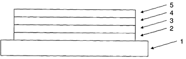
도 1은 유기 발광 소자를 도시하고;
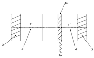
도 2는 OLED의 발광 기전을 도시한다.1 shows an organic light emitting element;
2 shows the light emission mechanism of the OLED.
도 1은 본 발명의 실시양태에 따른 OLED의 구조를 도시한다.1 shows the structure of an OLED according to an embodiment of the invention.
OLED는 투명 유리 또는 가소성 기판(1), 애노드(2), 캐소드(5), 및 애노드(2)와 캐소드(5) 사이에 제공된 정공 수송층(3) 및 발광층(4)을 포함한다. 추가 층, 예를 들어 전하 수송, 전하 주입 또는 전하 차단층이 애노드(2)와 캐소드 사이에 위치할 수 있다. 예를 들어 전자 수송층이 발광층(4) 및 캐소드(5) 사이에 제공될 수 있다.The OLED comprises a transparent glass or
도 2와 관련하여, 정공이 애노드(2)로부터 주입되고, 전자가 캐소드(5)로부터 주입된다. 정공 및 전하가 발광층(4)의 재조합 영역(4a)에서 재조합을 겪어서 방사성 붕괴를 겪는 여기자를 형성한다.With reference to FIG. 2, holes are injected from the
그러나, 정공 및 전자의 재조합에 의하여 형성된 모든 여기자가 방사성 붕괴를 겪게 되는 것은 아니고, 이들 여기자는 소자 수명에 해로울 수 있다. 특히, 단일항 또는 삼중항 여기자는 발광층(4)으로부터 정공 수송층(3) 내로 이동할 수 있다. 그리고, 여기자는 발광층(4)을 통과하여 정공 수송층(3)에 도달하는 여기자로부터 형성될 수 있다. 이들 여기자는 물질 또는 정공 수송층(3)의 물질과 상호작용할 수 있다. 본 발명자들은 이러한 상호작용이 소자의 작동 수명 및/또는 효율을 감소시킬 수 있음을 확인하였다.However, not all excitons formed by recombination of holes and electrons suffer from radioactive decay, and these excitons can be detrimental to device life. In particular, singlet or triplet excitons can migrate from the
재조합 영역(4a)이 정공 수송층(3) 사이의 계면에 인접한 경우에 발광층으로부터의 여기자 이동이 발생할 수 있다. 그리고, 삼중항 여기자는 전형적으로 상대적으로 긴 수명을 갖으며 재조합 영역 (4a)이 정공 수송층(3)과 발광층(4) 사이의 계면으로부터 상대적으로 먼 경우에도 정공 수송층(3) 내로 이동할 수 있다.Excitation of the exciton from the light emitting layer may occur when the
도 2는 여기자가 발광층으로부터 이동할 수 있는 정공 수송층을 갖는 OLED를 도시한다. 전자 수송층이 OLED의 발광층과 캐소드 사이에 존재하는 경우(정공 수송층은 존재하거나 존재하지 않을 수 있음), 여기자가 유사한 해로운 효과를 갖는 전자 수송층 내로 동일하게 이동할 수 있는 것으로 이해된다. 마찬가지로, 전자 수송층에 도달하는 정공은 전자와 재조합되어 전자 수송층에서 여기자를 형성시킨다.2 shows an OLED having a hole transport layer in which excitons can move from the light emitting layer. It is understood that when an electron transport layer is present between the light emitting layer and the cathode of the OLED (the hole transport layer may or may not be present), the excitons can equally move into the electron transport layer with similar deleterious effects. Likewise, holes reaching the electron transport layer recombine with electrons to form excitons in the electron transport layer.
본 발명자들은 정공 수송층(2)(및/또는 존재하는 경우 전자 수송층) 내에 발광 도펀트를 포함시킴으로써 소자 수명이 개선될 수 있음을 확인하였다. 어떠한 이론에도 구속되지 않기를 바라며, 수명의 개선은 발광 도펀트에 의한 정공 수송층 내의 여기자 흡수에 기인하며, 이는 광의 형성 중에 여기자가 에너지를 방출하도록 하는 것으로 믿어진다.The inventors have found that device lifetime can be improved by including a light emitting dopant in the hole transport layer 2 (and / or electron transport layer, if present). Without wishing to be bound by any theory, the improvement in lifetime is due to the exciton absorption in the hole transport layer by the luminescent dopant, which is believed to cause excitons to release energy during formation of light.
전하 수송층 내에 발광 도펀트가 존재하지 않는 대조 소자와 비교하여, 소자로부터 방출되는 광의 색에 대한 전하 수송층으로부터 방출된 광의 색의 효과를 최소화하기 위해 수많은 측정이 수행될 수 있다. 이러한 측정은 하기를 포함하지만 이에 제한되지는 않는다:In comparison to a control device in which there is no light emitting dopant in the charge transport layer, numerous measurements can be performed to minimize the effect of the color of light emitted from the charge transport layer on the color of light emitted from the device. Such measurements include, but are not limited to:
(i) 도펀트에 의해 방출되는 광의 양을 최소화하기 위하여 전하 수송층 내의 도펀트의 소량을 제공하는 것. 본 발명자들은 놀랍게도 아주 낮은(1 몰% 이하) 도핑 수준에서도 수명의 극적인 증가가 달성가능함을 발견하였다.(i) providing a small amount of dopant in the charge transport layer to minimize the amount of light emitted by the dopant. The inventors have found that a dramatic increase in life is surprisingly achievable even at very low (up to 1 mol%) doping levels.
(ii) 예를 들어 도 1 및 2에 도시된 바와 같이, 발광층과 전하 수송층이 접촉하는 경우, 전하 수송층에 도달하는 여기자의 수를 감소시키기 위하여 전하 수송층과 발광층의 계면에서 떨어진 곳에 발광층의 재조합 영역을 위치시키는 것. 이는 통상의 기술자에게 공지된 기술을 사용하여 수행될 수 있다. 예를 들어, 전하 수송층의 두께는 감소될 수 있고/있거나 발광층의 두께는 증가될 수 있다.(ii) When the light emitting layer and the charge transport layer are in contact with each other, for example, as shown in FIGS. 1 and 2, in order to reduce the number of excitons that reach the charge transport layer, a recombination region of the light emitting layer is located away from the interface of the charge transport layer and the light emitting layer. To locate it. This can be done using techniques known to those skilled in the art. For example, the thickness of the charge transport layer can be reduced and / or the thickness of the light emitting layer can be increased.
(iii) 전하 수송층에서, 발광층으로부터 방출되는 광과 동일하거나 실질적으로 동일한 색을 갖는 광을 방출하는 도펀트를 사용하는 것. 이는 예를 들어, 발광층 및 전하 수송층 모두에서 동일한 도펀트를 사용하는 것, 또는 동일하거나 실질적으로 동일한 광의 색을 방출하는 다른 도펀트를 사용하는 것을 수반할 수 있다.(iii) using a dopant in the charge transport layer that emits light having the same or substantially the same color as the light emitted from the light emitting layer. This may involve, for example, using the same dopant in both the light emitting layer and the charge transport layer, or using other dopants that emit the same or substantially the same color of light.
상기 측정 각각은 단독 또는 조합으로 사용될 수 있다.Each of the above measurements can be used alone or in combination.
전하 Majesty 수송층Transport layer
전하 수송층은 전하 수송 물질 및 발광 도펀트를 포함한다. 전하 수송 물질은 발광 도펀트의 여기된 상태 에너지 준위보다 높은 여기된 상태 에너지 준위를 갖는다. 특히, 형광 발광 도펀트의 경우에 전하 수송 물질의 단일항 여기된 상태 에너지 준위(S1)는 형광 발광 도펀트의 그것보다 높아야 하고 이로 인해 단일항 여기자는 전하 수송 물질에서 형광 발광 도펀트로 이동될 수 있다. 전하 수송 물질의 단일항 준위는 도펀트의 단일항 준위보다 0.01 eV 이상 높아야 하고, 더욱 바람직하게는 0.05 eV, 더더욱 바람직하게는 0.1 eV 이상 높다. 마찬가지로, 인광 발광 도펀트의 경우에 전하 수송 물질의 삼중항 여기된 상태 에너지 준위(T1)는 인광 발광 도펀트의 그것보다 높아야 하고 이로 인해 삼중항 여기자는 전하 수송 물질에서 인광 발광 도펀트로 이동될 수 있다. 전하 수송 물질의 삼중항 준위는 인광 도펀트의 삼중항 준위보다 0.01 eV 이상 높아야 하고, 더욱 바람직하게는 0.05 eV, 더더욱 바람직하게는 0.1 eV 이상 높다.The charge transport layer includes a charge transport material and a light emitting dopant. The charge transport material has an excited state energy level higher than the excited state energy level of the light emitting dopant. In particular, in the case of fluorescence dopants, the singlet excited state energy level (S 1 ) of the charge transport material must be higher than that of the fluorescence dopant, thereby allowing the singlet excitons to migrate from the charge transport material to the fluorescence dopant. . The singlet level of the charge transport material should be at least 0.01 eV higher than the singlet level of the dopant, more preferably at least 0.05 eV, even more preferably at least 0.1 eV. Likewise, in the case of a phosphorescent dopant, the triplet excited state energy level T 1 of the charge transport material must be higher than that of the phosphorescent dopant so that the triplet excitons can be transferred from the charge transport material to the phosphorescent dopant. . The triplet level of the charge transport material should be at least 0.01 eV higher than the triplet level of the phosphorescent dopant, more preferably 0.05 eV, even more preferably at least 0.1 eV.
전하 수송 물질은 소분자, 올리고머, 고분자, 덴드리머 또는 다른 물질일 수 있다. 전하 수송 물질이 중합체인 경우 이는 공액결합된 또는 비공액결합된 중합체일 수 있고, 전하 수송 단위체는 중합체 주쇄 또는 중합체 측쇄에 제공될 수 있다.The charge transport material may be a small molecule, oligomer, polymer, dendrimer or other material. If the charge transport material is a polymer, it may be a conjugated or unconjugated polymer, and charge transport units may be provided in the polymer backbone or polymer side chain.
정공 수송층은 바람직하게는 낮은 전자 친화도(2 eV 이하) 및 낮은 이온화도(5.8 eV 이하, 바람직하게는 5.7 eV 이하, 더욱 바람직하게는 5.6 eV 이하)를 갖는 물질을 포함한다. 전자 친화도와 이온화도는 전형적으로 문헌[Shirota and Kageyama, Chem. Rev. 2007, 107, 953-1010] 및 내부 참고문헌에 개시된 방법에 의하여 측정된다.The hole transport layer preferably comprises a material having low electron affinity (up to 2 eV) and low ionization (up to 5.8 eV, preferably up to 5.7 eV, more preferably up to 5.6 eV). Electron affinity and ionization are typically described in Shirota and Kageyama, Chem. Rev. 2007, 107, 953-1010 and internal references.
정공 수송 중합체는 아릴아민 반복 단위체, 특히 하기 화학식 (V)의 반복 단위체를 포함할 수 있다:The hole transport polymer may comprise arylamine repeating units, in particular repeating units of formula (V):

상기 식에서,Where
Ar1 및 Ar2는 각각의 경우 임의로 치환된 아릴 또는 헤테로아릴 기로부터 독립적으로 선택되고, n은 1 이상, 바람직하게는 1 또는 2이고, R은 H 또는 치환체, 바람직하게는 치환체이고, x 및 y는 각각 독립적으로 1, 2 또는 3이다.Ar 1 and Ar 2 are each independently selected from an optionally substituted aryl or heteroaryl group, n is at least 1, preferably 1 or 2, R is H or a substituent, preferably a substituent, x and y is independently 1, 2 or 3, respectively.
R은 바람직하게는 알킬, Ar3, 또는 Ar3 기의 분지쇄 또는 직쇄, 예를 들어 -(Ar3)r이고, 이때 Ar3은 각각의 경우 아릴 또는 헤테로아릴로부터 독립적으로 선택되고 r은 1 이상, 임의로 1, 2 또는 3이다.R is preferably a branched or straight chain, for example-(Ar 3 ) r of an alkyl, Ar 3 , or Ar 3 group, where Ar 3 is independently selected from aryl or heteroaryl in each case and r is 1 And optionally 1, 2 or 3.
Ar1, Ar2 및 Ar3 중 하나는 독립적으로 하나 이상의 치환체로 치환될 수 있다.One of Ar 1 , Ar 2 and Ar 3 may be independently substituted with one or more substituents.
바람직한 치환체는 하기로 구성된 R3 기로부터 선택된다:Preferred substituents are R 3 Is selected from:
알킬, 이때 하나 이상의 비인접 C 원자가 O, S, 치환된 N, C=O 또는 -COO-로 치환될 수 있고, 알킬 기의 하나 이상의 H 원자가 F 또는 하나 이상 의 R4 기로 임의로 치환된 아릴 또는 헤테로아릴로 치환될 수 있고,Alkyl, wherein one or more non-adjacent C atoms may be substituted with O, S, substituted N, C═O or —COO—, and one or more H atoms of the alkyl group optionally substituted with F or one or more R 4 groups, or May be substituted with heteroaryl,
하나 이상의 R4 기로 임의로 치환된 아릴 또는 헤테로아릴,Aryl or heteroaryl optionally substituted with one or more R 4 groups,
NR5, OR5 , SR5,NR 5 , OR 5 , SR 5 ,
플루오린, 니트로 및 시아노;Fluorine, nitro and cyano;
이때 각각의 R4는 독립적으로 하나 이상의 비인접 C 원자가 O, S, 치환된 N, C=O 또는 -COO-로 치환될 수 있고, 알킬 기의 하나 이상의 H 원자가 F로 치환될 수 있는 알킬이고, 각각의 R5는 독립적으로 알킬 및 하나 이상의 알킬 기로 임의로 치환된 아릴 또는 헤테로아릴로 구성된 군으로부터 선택된다.Wherein each R 4 is independently alkyl wherein one or more non-adjacent C atoms may be substituted with O, S, substituted N, C═O or —COO— and one or more H atoms of the alkyl group may be replaced with F , Each R 5 is independently selected from the group consisting of alkyl and aryl or heteroaryl optionally substituted with one or more alkyl groups.
R은 교차결합가능한 기, 예를 들어 중합가능한 이중 결합, 예를 들어 비닐 또는 아크릴레이트 기, 또는 벤조사이클로부탄 기를 포함하는 기를 포함할 수 있다.R may comprise a crosslinkable group, for example a group comprising a polymerizable double bond such as a vinyl or acrylate group, or a benzocyclobutane group.
화학식 (V)의 반복 단위체 내의 아릴 또는 헤테로아릴 기 중 어느 하나는 직접 결합 또는 2가 결합 원자 또는 기에 의해 결합될 수 있다. 바람직한 2가 결합 원자 또는 기는 O, S; 치환된 N; 및 치환된 C를 포함한다.Either aryl or heteroaryl group in the repeating unit of formula (V) may be bonded by a direct bond or a divalent bond atom or group. Preferred divalent bonding atoms or groups are O, S; Substituted N; And substituted C.
존재하는 경우, R3, R4 또는 2가 결합 기의 치환된 N 또는 치환된 C는 독립적으로 각각의 경우 각각 NR6 또는 CR6 2로 각각 치환될 수 있고 이때 R6는 알킬 또는 임의로 치환된 아릴 또는 헤테로아릴이다. 아릴 및 헤테로 기 R6의 임의적 치환체는 R4 또는 R5로부터 선택될 수 있다.If present, the substituted N or substituted C of the R 3 , R 4 or divalent bond group can be independently substituted in each case with NR 6 or CR 6 2 , respectively, wherein R 6 is alkyl or optionally substituted Aryl or heteroaryl. Optional substituents of the aryl and hetero groups R 6 may be selected from R 4 or R 5 .
바람직한 배열에서, R은 Ar3이고 각각의 Ar1, Ar2 및 Ar3은 독립적으로 하나 이상의 C1 -20 알킬 기로 임의로 치환된다.In a preferred arrangement, R is Ar 3, and each of Ar 1, Ar 2 and Ar 3 are independently optionally substituted with one or more C 1 -20 alkyl.
화학식 1을 만족시키는 특히 바람직한 단위체는 하기 화학식 1 내지 화학식 3의 단위체를 포함한다:Particularly preferred

상기 식에서, Ar1 및 Ar2는 상술한 바와 같고; Ar 3은 임의로 치환된 아릴 또는 헤테로아릴이다.Wherein Ar < 1 > and Ar < 2 > are as defined above; Ar 3 is optionally substituted aryl or heteroaryl.
존재하는 경우 바람직한 Ar3의 치환체는 Ar1 및 Ar2에 기술한 바와 같은 치환체, 특히 알킬 및 알콕시 기를 포함한다.Preferred substituents of Ar 3 , if present, include substituents as described for Ar 1 and Ar 2 , in particular alkyl and alkoxy groups.
Ar1, Ar 2 및 Ar3은 바람직하게는 페닐이고, 이들 각각은 독립적으로 상술한 하나 이상의 치환체로 치환될 수 있다.Ar 1 , Ar 2 and Ar 3 are preferably phenyl, each of which may be independently substituted with one or more substituents described above.
다른 바람직한 배열에서, 화학식 (V)의 아릴 또는 헤테로아릴 기는 페닐이고, 각각의 페닐 기는 하나 이상의 알킬 기로 임의로 치환된다.In another preferred arrangement, the aryl or heteroaryl group of formula (V) is phenyl, and each phenyl group is optionally substituted with one or more alkyl groups.
다른 바람직한 배열에서, Ar1, Ar 2 및 Ar3은 페닐이고, 이들 각각은 하나 이상의 C1 -20 알킬 기로 치환될 수 있고, r = 1이다.In another preferred arrangement, and Ar 1, Ar 2 and Ar 3 are phenyl, each of which can be optionally substituted with one or more C 1 -20 alkyl, and r = 1.
다른 바람직한 배열에서, Ar1 및 Ar 2는 페닐이고, 이들 각각은 하나 이상의 C1-20 알킬 기로 치환될 수 있고, R은 각각의 페닐이 하나 이상의 알킬 기로 치환될 수 있는 3,5-다이페닐벤젠이다.In another preferred arrangement, Ar 1 and Ar 2 are phenyl, each of which may be substituted with one or more C 1-20 alkyl groups, and R is 3,5-diphenyl, wherein each phenyl may be substituted with one or more alkyl groups Benzene.
또 다른 바람직한 배열에서, Ar1, Ar 2 및 Ar3은 페닐이고, 이들 각각은 하나 이상의 C1 -20 알킬 기로 치환될 수 있고, r =1이고 Ar1 및 Ar 2는 O 또는 S 원자에 의하여 결합된다.In another preferred arrangement, and Ar 1, Ar 2 and Ar 3 are phenyl, each of which can be optionally substituted with one or more C 1 -20 alkyl, r = 1 and Ar 1 and Ar 2, by O or S atom Combined.
다른 바람직한 배열에서, Ar1, Ar 2 및 Ar3은 페닐이고 이들 각각은 하나 이상의 알킬 기, 특히 C1 -20 알킬로 치환될 수 있다.In another preferred arrangement, Ar 1, Ar 2 and Ar 3 is phenyl and each of which may be substituted with one or more alkyl groups, especially C 1 -20 alkyl.
구체적인 정공 수송 단위체는 하기 구조를 포함한다:Specific hole transport monomers include the following structures:


상기 식에서,Where
R7은 각각의 경우 독립적으로 H 또는 치환체, 예를 들어 H 또는 R3이다. R 7 in each occurrence is independently H or a substituent, for example H or R 3 .
2극성 기의 예는 하기 구조를 포함한다:Examples of dipolar groups include the following structures:


상기 식에서,Where
R7은 상술한 바와 같다.R 7 is as described above.
상기 중합체는 호모폴리머일 수 있고 또는 이는 99 몰% 이하, 바람직하게는 70 몰% 이하, 더욱 바람직하게는 50 몰% 이하의 양으로 화학식 (V)의 반복 단위체를 포함하는 공중합체일 수 있다. 이러한 백분율은 하나 이상의 유형의 화학식 (V)의 반복 단위체가 사용되는 경우에 중합체 중에 존재하는 아릴아민 단위체의 총 수에 적용된다.The polymer may be a homopolymer or it may be a copolymer comprising repeating units of formula (V) in an amount of up to 99 mol%, preferably up to 70 mol%, more preferably up to 50 mol%. This percentage applies to the total number of arylamine units present in the polymer when one or more types of repeat units of formula (V) are used.
정공 수송 중합체가 공중합체인 경우, 적합한 공중합체는 화학식 (V)의 반복 단위체 및 아릴렌 또는 헤테로아릴렌 공반복 단위체를 포함하는 공중합체를 포함한다. 아릴렌 반복 단위체의 예는 예를 들어 문헌[Adv. Mater. 200012(23) 1737-1750]에 개시되어 있고, 문헌[J. Appl. Phys. 1996, 79, 934]에 개시된 1,4-페닐렌 반복 단위체; 유럽특허출원공개 제 0 842 208 호에 개시된 플루오렌 반복 단위체; 예를 들어 문헌[Macromolecules 2000, 33(6), 2016-2020]에 개시된 인데노플루오렌 반복 단위체; 및 예를 들어 유럽특허출원공개 제 0 707 020 호에 개시된 스피노플루오렌 반복 단위체를 포함한다. 이들 반복 단위체 각각은 임의로 치환된다. 치환체의 예는 가용성 기, 예를 들어 C1 -20 알킬 기 또는 알콕시; 전자 끄는 기, 예를 들어 플루오린, 니트로 또는 시아노; 및 중합체의 유리 전이 온도(Tg)를 증가시키는 치환체를 포함한다.When the hole transport polymer is a copolymer, suitable copolymers include copolymers comprising repeating units of formula (V) and arylene or heteroarylene co-repeat units. Examples of arylene repeating units are described, for example, in Adv. Mater. 200012 (23) 1737-1750, and J. Chem. Appl. Phys. 1996, 79, 934, 1,4-phenylene repeat unit; Fluorene repeat units disclosed in EP 0 842 208; Indenofluorene repeat units as disclosed, for example, in Macromolecules 2000, 33 (6), 2016-2020; And spinofluorene repeat units as disclosed, for example, in European Patent Application Publication No. 0 707 020. Each of these repeat units is optionally substituted. Examples of substituents are soluble group, e.g., C 1 -20 alkyl group or an alkoxy group; Electron withdrawing groups such as fluorine, nitro or cyano; And a substituent that increases the glass transition temperature (Tg) of the polymer.
특히 바람직한 아릴렌 반복 단위체는 임의로 치한된 2,7-결합된 플루오렌, 가장 바람직하게는 gkrl 화학식 IV의 반복 단위체를 포함한다:Particularly preferred arylene repeating units include optionally substituted 2,7-linked fluorene, most preferably gkrl repeating units of formula IV:

상기 식에서,Where
상기 식에서, R1 및 R2는 독립적으로 H 또는 치환체이고 이때 R 1 및 R2는 결합되어 환을 형성할 수 있다. R1 및 R2 는 바람직하게는 수소; 하나 이상의 비인접 C 원자가 O, S, N, C=O 또는 -COO-로 치환될 수 있는 임의로 치환된 알킬; 임의로 치환된 아릴 또는 헤테로아릴, 특히 하나 이상의 알킬 기, 예를 들어 C1 -20 알킬로 치환된 아릴 또는 헤테로아릴; 및 임의로 치환된 아릴알킬 또는 헤테로아릴알킬로 구성된 군으로부터 선택된다. 더욱 바람직하게는, 하나 이상의 R1 및 R2는 임의로 치환된 알킬, 예를 들어 C1-C20 알킬, 또는 아릴, 특히 페닐 기를 포함한다. R1 및 R2는 각각 독립적으로 직쇄 또는 분지쇄의 아릴 또는 헤테로아릴 기를 포함하고, 이들 기 각각은 독립적으로 예를 들어 상술한 화학식 (Ar3)r 기로 치환될 수 있다.Wherein R 1 and R 2 are independently H or a substituent, where R 1 and R 2 may be joined to form a ring. R 1 and R 2 are preferably hydrogen; Optionally substituted alkyl wherein one or more non-adjacent C atoms may be substituted with O, S, N, C═O or —COO—; An optionally substituted aryl or heteroaryl, in particular one or more alkyl groups such as an aryl or heteroaryl substituted with a C 1 -20 alkyl; And optionally substituted arylalkyl or heteroarylalkyl. More preferably, at least one R 1 and R 2 comprises an optionally substituted alkyl, for example C 1 -C 20 alkyl, or aryl, in particular a phenyl group. R 1 and R 2 each independently comprise a straight or branched aryl or heteroaryl group, each of which may be independently substituted, for example, with the above-described formula (Ar 3 ) r group.
R1 또는 R2가 아릴 또는 헤테로아릴을 포함하는 경우에, 바람직한 임의적 치환체는 하나 이상의 비인접 C 원자가 O, S, N, C=O 또는 -C(=O)O-로 치환될 수 있는 알킬 기를 포함한다.When R 1 or R 2 comprises aryl or heteroaryl, preferred optional substituents are alkyl wherein one or more non-adjacent C atoms may be substituted with O, S, N, C═O or —C (═O) O—. Contains groups.
R1 및/또는 R2는 교차결합가능한 기, 예를 들어 중합가능한 이중 결합, 예를 들어 비닐 또는 아크릴레이트 기, 또는 벤조사이클로부탄 기를 포함하는 기를 포함할 수 있다.R 1 and / or R 2 may comprise crosslinkable groups such as polymerizable double bonds such as vinyl or acrylate groups, or groups comprising benzocyclobutane groups.
플루오렌 단위체에서 R1 및 R2가 아닌 임의의 치환체는 바람직하게는 하나 이상의 비인접 C 원자가 O, S, 치환된 N, C=O 또는 -COO-로 치환될 수 있는 알킬, 임의로 치환된 아릴, 임의로 치환된 헤테로아릴, 알콕시, 알킬티오, 플루오린, 시아노 및 아릴알킬로 구성된 군으로부터 선택된다.Any substituent other than R 1 and R 2 in the fluorene unit is preferably alkyl, optionally substituted aryl, wherein one or more non-adjacent C atoms may be substituted with O, S, substituted N, C═O or —COO—. , Optionally substituted heteroaryl, alkoxy, alkylthio, fluorine, cyano and arylalkyl.
본 명세서에서 사용된 "아릴(렌)" 및 "헤테로아릴(렌)"은 각각 융합 및 비융합된 아릴 및 헤테로아릴 모두를 포함한다.As used herein, "aryl (ene)" and "heteroaryl (ene)" include both fused and unfused aryl and heteroaryl, respectively.
발광이 하나 이상의 인광 에미터(emitter)에서 일어나는 경우, 바람직한 아릴렌 반복 단위체는 임의로 치환된 페닐렌 반복 단위체, 예를 들어 1,4-페닐렌이다. 페닐렌 반복 단위체는 상술한 하나 이상의 R1 기로 치환될 수 있고, 이때 각각의 R1은 독립적으로 각각의 경우 H 또는 치환체, 예를 들어 알킬, 예를 들어 하기 화학식 (VII)의 반복 단위체이다:When luminescence occurs in one or more phosphorescent emitters, the preferred arylene repeating units are optionally substituted phenylene repeating units, for example 1,4-phenylene. Phenylene repeating units may be substituted with one or more R 1 groups as described above, wherein each R 1 is independently in each occurrence H or a substituent, eg alkyl, for example a repeating unit of formula (VII):

상기 식에서,Where
R1 및 R2는 동일하거나 상이하고 화학식 (IV)의 반복 단위체를 참조로 상술한 바와 같다.R 1 and R 2 are the same or different and as described above with reference to the repeating unit of formula (IV).
공액결합된 전하 수송 중합체의 제조를 위해 바람직한 방법은, 금속 착체 촉매의 금속 원자가 단량체의 아릴 또는 헤테로아릴 기 및 이탈기 사이에 삽입되는, "금속 삽입"을 포함한다. 예시적인 금속 삽입은, 스즈키 중합(예를 들어, 국제특허출원공개 제 WO 00/53656 호에서 기술함) 및 야마모토 중합(예를 들어, 문헌[T. Yamamoto, "Electric ally Conducting And Thermally Stable π- Conjugated Poly(arylene)s Prepared by Organometallic Process es", Progress in Polymer Science 1993, 17, 1153-1205]에서 기술함)이다. 야마모토 중합의 경우, 니켈 착체 촉매가 사용되고, 스즈키 중합의 경우, 팔라듐 착체 촉매가 사용된다.Preferred methods for the preparation of conjugated charge transport polymers include " metal insertion ", wherein the metal atoms of the metal complex catalyst are inserted between the aryl or heteroaryl groups and leaving groups of the monomers. Exemplary metal insertions include Suzuki polymerisation (eg, described in WO 00/53656) and Yamamoto polymerisation (eg, T. Yamamoto, "Electrically Conducting And Thermally Stable π-). Conjugated Poly (arylene) s Prepared by Organometallic Processes ", Progress in Polymer Science 1993, 17, 1153-1205). In the case of Yamamoto polymerization, a nickel complex catalyst is used, and in the case of Suzuki polymerization, a palladium complex catalyst is used.
예를 들어, 야마모토 중합에 의한 선형 중합체의 합성에서, 2개의 반응성 할로겐 기를 갖는 단량체가 사용된다. 유사하게, 스즈키 중합의 방법에 따라, 하나 이상의 반응성 기가 붕소 유도 기, 예를 들어 붕소산 또는 붕소산 에스터이고, 다른 반응성 기는 할로겐이다. 바람직한 할로겐은 염소, 브롬 및 요오드, 가장 바람직하게는 브롬이다.For example, in the synthesis of linear polymers by Yamamoto polymerization, monomers having two reactive halogen groups are used. Similarly, according to the method of Suzuki polymerization, the at least one reactive group is a boron derivative group such as boric acid or boric acid ester and the other reactive group is halogen. Preferred halogens are chlorine, bromine and iodine, most preferably bromine.
따라서, 본원 명세서 전반에 걸쳐서 설명한 반복 단위체는 적합한 이탈기를 보유하는 단량체로부터 유도될 수 있음을 이해할 것이다. 유사하게, 말단 기 또는 측쇄 기는 적합한 이탈기의 반응에 의해 중합체에 결합될 수 있다. Accordingly, it will be appreciated that the repeat units described throughout this specification may be derived from monomers having suitable leaving groups. Similarly, end groups or side chain groups can be linked to the polymer by reaction of suitable leaving groups.
스즈키 중합은 입체규칙성, 블록 및 랜덤 공중합체를 제조하기 위해서 사용될 수 있다. 특히, 단독중합체 또는 랜덤 공중합체는, 하나의 반응성 기가 할로겐이고 다른 반응성 기가 붕소 유도체 기인 경우, 제조될 수 있다. 다르게는, 제 1 단량체의 반응성 기 둘다가 붕소이고 제 2 단량체의 반응성 기 둘다가 할로겐인 경우, 블록 또는 입체규칙성, 특히 AB 공중합체가 제조될 수 있다. Suzuki polymerization can be used to prepare stereoregularity, block and random copolymers. In particular, homopolymers or random copolymers can be prepared when one reactive group is a halogen and the other reactive group is a boron derivative. Alternatively, block or stereoregular, in particular AB copolymers can be prepared when both reactive groups of the first monomer are boron and both reactive groups of the second monomer are halogen.
할라이드의 대안으로서, 금속 삽입에 참여할 수 있는 또 다른 이탈기는 토실레이트, 메실레이트 및 트라이플레이트를 포함한다.As an alternative to halides, other leaving groups that may participate in metal insertion include tosylate, mesylate and triflate.
전자 수송층은 바람직하게는 높은 전자 친화도(1.8 eV 이상, 바람직하게는 2 eV 이상, 더욱 바람직하게는 2.2 eV 이상) 및 높은 이온화도(5.8 eV 이상)를 갖는 물질을 포함한다. 적합한 전자 수송 기는 예를 들어 문헌[Shirota and Kageyama, Chem. Rev. 2007, 107, 953-1010]에 개시된 기를 포함한다.The electron transport layer preferably comprises a material having a high electron affinity (1.8 eV or more, preferably 2 eV or more, more preferably 2.2 eV or more) and high ionization degree (5.8 eV or more). Suitable electron transport groups are described, for example, in Shirota and Kageyama, Chem. Rev. 2007, 107, 953-1010.
전자 수송 반복 단위체는 하기 화학식 (II)를 포함하는 기를 포함한다:Electron transport repeat units include groups comprising the formula (II):

상기 식에서,Where
Ar1 및 Ar2는 상술한 바와 같고; r은 1 이상, 바람직하게는 1 내지 3이고, Het은 높은 전자 친화도를 갖는 임의로 치환된 헤테로아릴 기를 나타낸다. Het의 임의적 치환체는 상기 R과 관련하여 기술한 바와 같다. Het이 아릴 또는 헤테로아릴 기로 치환된 경우, 이는 상술한 -(Ar3)r 기일 수 있다.Ar 1 and Ar 2 are as described above; r is at least 1, preferably 1 to 3, and Het represents an optionally substituted heteroaryl group having a high electron affinity. Optional substituents of Het are as described for R above. When Het is substituted with an aryl or heteroaryl group, it may be the aforementioned-(Ar 3 ) r group.
높은 전자 친화도를 갖는 적합한 헤테로아릴은 트리아진, 피리미딘, 옥사다이아졸, 피리딘, 트리아졸, 트리아릴보란, 설폭사이드 및 실롤, 특히 하나 이상의 치환체 기로 치환된 트리페닐트리아진, 예를 들어 하나 이상의 C1-C20 알킬 기로 치환된 트리페닐 트리아진을 포함한다.Suitable heteroaryls having high electron affinity are triazines, pyrimidines, oxadiazoles, pyridines, triazoles, triarylboranes, sulfoxides and silols, in particular triphenyltriazines substituted with one or more substituent groups, for example one Triphenyl triazine substituted with the above C 1 -C 20 alkyl group.
전자 수송 기의 예는 하기 구조를 포함한다:Examples of electron transport groups include the following structures:


상기 식에서,Where
R7은 상술한 바와 같다.R 7 is as described above.
다른 적합한 전자 수송 물질은 임의로 치환된 케톤, 다이아릴설폭사이드, 및 포스핀 옥사이드를 포함한다.Other suitable electron transport materials include optionally substituted ketones, diarylsulfoxides, and phosphine oxides.

상기 식에서,Where
R7은 상술한 바와 같다.R 7 is as described above.
다른 적합한 전자 수송 물질은 임의로 치환된 보란, 예를 들어Other suitable electron transport materials include optionally substituted boranes, for example

를 포함한다..
상기 식에서,Where
R7은 상술한 바와 같다.R 7 is as described above.
특정 기가 정공 및 전자 수송 기 모두로 작용할 수 있다. 이들은 소위 2극성 기이고 카바졸, 특히 Ar1, Ar 2 및 Ar3 중 두개가 직접 C-C 결합에 의하여 결합된 페닐인 화학식 1, 2 및 3의 기를 포함한다. 2극성 기는 전형적으로 약 2 eV의 전자 친화도 및 약 5.8 eV의 이온화도를 갖는다.Certain groups can act as both hole and electron transport groups. These include the groups of
전자 친화도 및 이온화도에 따라, 전하 수송층은 정공 및 전자를 수송할 수도 있고 다른 정공 및 전자를 차단할 수도 있다.Depending on electron affinity and ionization, the charge transport layer may transport holes and electrons and block other holes and electrons.
전하 수송층 내에서 형광 또는 인광 발광 도펀트로서 사용될 수 있는 물질은 하기 화학식 (III)의 임의로 치환된 복합체를 포함하는 금속 복합체일 수 있다:Materials that can be used as fluorescent or phosphorescent dopants in the charge transport layer can be metal complexes including optionally substituted complexes of formula (III):

상기 식에서,Where
M은 금속이고; L1, L2 및 L3은 배위 기이고; q는 정수이고; r 및 s는 각각 독립적으로 0 또는 정수이고; (a. q)+(b . r)+(c. s)의 합은 M에서 이용가능한 배위 부위의 수와 같고, 이때 a는 L1의 배위 부위의 수이고, b는 L2의 배위 부위의 수이고, c는 L3의 배위 부위의 수이다.M is a metal; L 1 , L 2 and L 3 are a coordinating group; q is an integer; r and s are each independently 0 or an integer; The sum of (a. q) + (b.r) + (c.s) is equal to the number of coordination sites available at M, where a is the number of coordination sites of L 1 and b is the coordination site of L 2 C is the number of coordination sites of L 3 .
무거운 원소 M은 강한 스핀-오빗(spin-orbit) 커플링을 유도하여 빠른 계내 가교 및 삼중항 또는 더 높은 상태으로부터의 발산(인광)을 가능하게 한다. 적합한 중금속 M은 다음을 포함한다:The heavier element M induces strong spin-orbit coupling to enable fast in-situ crosslinking and divergence from the triplet or higher state (phosphorescence). Suitable heavy metals M include:
-란탄계 금속, 예를 들어 세륨, 사마륨, 유로퓸, 테르븀, 디스프로슘, 툴륨, 에르븀 및 네오디뮴 및Lanthanum-based metals such as cerium, samarium, europium, terbium, dysprosium, thulium, erbium and neodymium and
-d-블록 금속, 특히 2 및 3열의 것들, 즉 원소 39 내지 48 및 72 내지 80, 특히 루테늄, 로듐, 팔라듐, 레늄, 오스뮴, 이리듐, 백금 및 금. 이리듐이 특히 바람직하다. -d-block metals, especially those in
f-블록 금속에 적합한 배위 기는 산소 또는 질소 공여체 시스템, 예를 들어 카르복실산, 1,3-디케토네이트, 히드록시 카르복실산, 스키프(Schiff) 염기, 예컨대 아실 페놀 및 이미노아실 기를 포함한다. 공지된 바와 같이 발광 란탄계 금속 복합체는 금속 이온의 제1 여기 상태보다 더 높은 삼중항 여기 에너지 수준을 갖는 증감(sensitizing) 기를 필요로 한다. 금속의 f-f 전이로부터의 발산 및 발산 색은 금속의 선택에 의해 결정된다. 날카로운 발산은 일반적으로 좁아 디스플레이 적용에 유용한 순수한 색 발산을 초래한다.Coordinating groups suitable for f-block metals are oxygen or nitrogen donor systems, for example carboxylic acids, 1,3-diketonates, hydroxy carboxylic acids, Schiff bases such as acyl phenols and iminoacyl groups Include. As is known, luminescent lanthanide-based metal complexes require sensitizing groups with higher triplet excitation energy levels than the first excited state of the metal ions. The divergence and divergence color from the f-f transition of the metal is determined by the choice of metal. Sharp divergence is generally narrow resulting in pure color divergence useful for display applications.
d-블록 금속은 특히 삼중항 여기 상태로부터의 발산에 적합하다. 이들 금속은 탄소 또는 질소 공여체와 유기금속 복합체, 예를 들어 포르피린 또는 하기 화학식 (VI)의 두 자리 리간드를 형성한다:d-block metals are particularly suitable for divergence from triplet excited states. These metals form organometallic complexes, such as porphyrins or bidentate ligands of formula (VI) with carbon or nitrogen donors:

상기 식에서, Where
Ar4 및 Ar5는 동일하거나 상이할 수 있고 임의적으로 치환된 아릴 및 헤테로아릴로부터 독립적으로 선택되고, Ar4 및 Ar5는 함께 융합될 수 있고;Ar 4 and Ar 5 may be the same or different and are independently selected from optionally substituted aryl and heteroaryl, and Ar 4 and Ar 5 may be fused together;
X1 및 Y1은 동일하거나 상이할 수 있고 탄소 및 질소로부터 독립적으로 선택된다.X 1 and Y 1 may be the same or different and are independently selected from carbon and nitrogen.
X1이 탄소이고 Y1이 질소인 리간드가 특히 바람직하다.Particular preference is given to ligands wherein X 1 is carbon and Y 1 is nitrogen.
두 자리 리간드의 예를 하기에 도시한다:Examples of bidentate ligands are shown below:

각각의 Ar4 및 Ar5는 하나 이상의 치환체를 갖는다. 이들 치환체 중 둘 이상은 연결되어 환, 예를 들어 방향족 환을 형성할 수 있다. 특히 바람직한 치환체는 국제특허출원공개 제 WO 02/45466 호, 제 WO 02/44189호, 미국특허출원공개 제 2002-117662 호 및 미국특허출원공개 제 2002-182441 호에 개시된 복합체의 발산을 청색 이동시키는데 사용될 수 있는 플루오르 또는 트리플루오로메틸; 일본특허출원공개 제 2002-324679 호에 개시된 알킬 또는 알콕시 기; 국제특허출원공개 제 WO 02/81448 호에 개시된 발산 물질로 사용될 때 복합체로 정공 수송을 돕는데 사용될 수 있는 카르바졸; 국제특허출원공개 제 WO 02/68435 호 및 유럽특허출원공개 제 1 245 659 호에 개시된 추가 기의 부착을 위해 리간드를 기능화하는데 이용될 수 있는 브롬, 염소 또는 요오드; 및 국제특허출원공개 제 WO 02/66552 호에 개시된 금속 복합체의 용액 가공성을 수득하거나 증가시키는데 사용될 수 있는 덴드론을 포함한다. Each Ar 4 and Ar 5 has one or more substituents. Two or more of these substituents may be linked to form a ring, for example an aromatic ring. Particularly preferred substituents are used to blue shift the divergence of the complexes disclosed in WO 02/45466, WO 02/44189, US Patent Application Publication 2002-117662 and US Patent Application Publication 2002-182441. Fluoro or trifluoromethyl which may be used; Alkyl or alkoxy groups disclosed in Japanese Patent Application Laid-Open No. 2002-324679; Carbazole, which may be used to aid hole transport into the composite when used as a diverging material disclosed in WO 02/81448; Bromine, chlorine or iodine, which can be used to functionalize ligands for the attachment of further groups disclosed in WO 02/68435 and
발광 덴드리머는 전형적으로 하나 이상의 덴드론에 결합된 발광 코어를 포함하고, 이 때 각각의 덴드론은 분지점 및 2개 이상의 수지상 분지를 포함한다. 바람직하게는 덴드론은 적어도 부분적으로 공액되고, 코어 및 수지상 분지의 하나 이상은 아릴 또는 헤테로아릴 기를 포함한다.Luminescent dendrimers typically comprise a luminescent core coupled to one or more dendrons, each dendron comprising a branch point and two or more dendritic branches. Preferably the dendron is at least partially conjugated and at least one of the core and dendritic branches comprises aryl or heteroaryl groups.
d-블록 원소와 사용하기에 적합한 다른 리간드는 디케토네이트, 특히 아세틸아세토네이트(acac); 트리아릴포스핀 및 피리딘을 포함하고, 각각은 치환될 수 있다.Other ligands suitable for use with the d-block element include diketonates, in particular acetylacetonate (acac); Triarylphosphines and pyridine, each of which may be substituted.
주요 기 금속 복합체는 리간드 기반 또는 전하 전달 발산을 나타낸다. 이 복합체에 있어서 발산 색은 금속 뿐만 아니라 리간드 선택에 의해 결정된다.The major base metal complexes exhibit ligand based or charge transfer divergence. The divergence color in this complex is determined by the ligand selection as well as the metal.
광범위한 형광 저분자량 금속 복합체가 공지되어 있고 유기 발광 장치에서 시연되었다(예를 들어 문헌[Macromol. Sym. 125 (1997) 1-48], 미국특허 제 5,150,006 호, 미국특허 제 6,083,634 호 및 미국특허 제 5,432,014 호 참조). 2가 또는 3가 금속을 위한 적합한 리간드는 다음을 포함한다: 예를 들어 산소-질소 또는 산소-산소 공여 원자를 갖는 옥시노이드(oxinoid), 일반적으로 치환체 산소 원자 또는 치환체 질소 원자를 갖는 환 질소 원자 또는 치환체 산소 원자를 갖는 산소 원자, 예를 들어 8-히드록시퀴놀레이트 및 히드록시퀴녹살리놀-10-히드록시벤조(h)퀴놀리네이토(II), 벤자졸(III), 스키프 염기, 아조인돌, 크로몬 유도체, 3-히드록시플라본, 및 카르복실산, 예를 들어 살리실레이토 아미노 카르복실레이트 및 에스테르 카르복실레이트. 임의적인 치환체는 발산 색을 변경시킬 수 있는 방향족 환 상의 할로겐, 알킬, 알콕시, 할로알킬, 시아노, 아미노, 아미도, 설포닐, 카르보닐, 아릴 또는 헤테로아릴을 포함한다. A wide range of fluorescent low molecular weight metal complexes are known and have been demonstrated in organic light emitting devices (see, eg, Macromol. Sym. 125 (1997) 1-48), US Pat. No. 5,150,006, US Pat. No. 6,083,634 and US Pat. 5,432,014). Suitable ligands for divalent or trivalent metals include, for example, oxygen-nitrogen or oxinoids with oxygen-oxygen donor atoms, generally ring nitrogen atoms with substituent oxygen atoms or substituent nitrogen atoms Or oxygen atoms having substituent oxygen atoms, for example 8-hydroxyquinolate and hydroxyquinoxalinol-10-hydroxybenzo (h) quinolinato (II), benzazole (III), skip base , Azoindole, chromone derivatives, 3-hydroxyflavones, and carboxylic acids such as salicylate amino carboxylate and ester carboxylate. Optional substituents include halogen, alkyl, alkoxy, haloalkyl, cyano, amino, amido, sulfonyl, carbonyl, aryl or heteroaryl on aromatic rings that can alter the divergence color.
발광 안트라센 반복 단위체의 예는 하기 화학식 (VIII)을 포함한다:Examples of luminescent anthracene repeat units include formula (VIII):

상기 식에서,Where
d, e 및 f는 독립적으로 0, 1, 2 또는 3이고 R8, R9 및 R10은 각각의 경우 하기로부터 독립적으로 선택된다:d, e and f are independently 0, 1, 2 or 3 and R 8 , R 9 and R 10 are each independently selected from:
Ar, 이때 Ar은 할로겐, CN, 및 알킬로부터 선택된 하나 이상의 치환체로 임의로 치환된 아릴 또는 헤테로아릴로 구성된 군으로부터 선택되고, 알킬 기의 하나 이상의 비인접 C 원자가 O, S, N, C=O 또는 -C(=O)O로 치환될 수 있고, 하나 이상의 알킬 기의 H 원자는 할로겐으로 치환될 수 있으며; 및Ar, wherein Ar is selected from the group consisting of aryl or heteroaryl, optionally substituted with one or more substituents selected from halogen, CN, and alkyl, wherein at least one non-adjacent C atom of the alkyl group is O, S, N, C═O or May be substituted with —C (═O) O, and the H atoms of one or more alkyl groups may be substituted with halogen; And
알킬, 이때 알킬 기의 하나 이상의 비인접 C 원자가 O, S, N, C=O 또는 -COO-로 치환될 수 있고, 알킬 기의 하나 이상의 H 원자는 할로겐 또는 Ar로 치환될 수 있다.Alkyl, wherein one or more non-adjacent C atoms of the alkyl group may be substituted with O, S, N, C═O or —COO—, and one or more H atoms of the alkyl group may be substituted with halogen or Ar.
페릴렌의 예는 하기 화학식 (IX)를 갖는다:Examples of perylene have the following formula (IX):

상기 식에서,Where
R1' 내지 R4'는 임의적인 치환체, 예를 들어 알킬, 예를 들어 C1 -20 알킬, 임의로 치환된 아릴, 예를 들어 임의로 치환된 페닐, 알콕시, 티오에터 및 아민으로 구성된 군으로부터 선택된 치환체이다. R 1 'to R 4' is an arbitrary substituent, for example, alkyl, such as C 1 -20 alkyl, optionally substituted aryl, such as optionally from phenyl, alkoxy, the group consisting of a foundation and the amine substituted thio Selected substituent.
방출형 페릴렌이 중합체의 반복 단위체로서 존재하는 경우, 이는 하기 화학식 (X)를 갖는다:When released perylenes are present as repeating units of the polymer, they have the formula (X):

상기 식에서, R5'는 직접 결합 또는 임의로 치환된 2가 결합 기, 예를 들어 임의로 치환된 페닐이다.Wherein R 5 ′ is a direct bond or an optionally substituted divalent bond group, for example optionally substituted phenyl.
형광 발광 도펀트의 다른 예는 하기 화학식 (XI)의 반복 단위체이다:Another example of a fluorescence dopant is a repeating unit of formula (XI):

상기 식에서,Where
Ar1 및 Ar3은 상술한 바와 같고, Ar6은 하나 이상의 치환체, 예를 들어 임의로 치환된 안트라센으로 치환될 수 있는 융합된 방향족 또는 헤테로방향족 기이다. 치환체는 상술한 R3 기로부터 선택될 수 있다.Ar 1 and Ar 3 are as described above and Ar 6 is a fused aromatic or heteroaromatic group which may be substituted with one or more substituents, for example an optionally substituted anthracene. Substituents may be selected from the R 3 groups described above.
발광 도펀트는 발광층의 발광 컴포넌트와 실질적으로 동일한 색을 방출할 수 있다. 발광 도펀트는발광층의 발광 컴포넌트와 실질적으로 동일한 코어 구조를 가질 수 있고; 예를 들어 발광 도펀트는 하나 이상의 치환체로 치환된 코어 구조(예를 들어 페릴렌 기, 안트라센 기 또는 상술한 금속 복합체)를 포함할 수 있다. 동일한 코어 구조는 동일한 치환체가 있거나 없이, 발광층의 발광 컴포넌트 중에 존재할 수 있다.The light emitting dopant can emit substantially the same color as the light emitting components of the light emitting layer. The light emitting dopant may have a core structure substantially the same as the light emitting component of the light emitting layer; For example, the luminescent dopant may comprise a core structure (eg, a perylene group, an anthracene group, or a metal complex described above) substituted with one or more substituents. The same core structure may be present in the light emitting component of the light emitting layer, with or without the same substituent.
전하 수송층은 하나 이상의 발광 도펀트를 함유할 수 있다.The charge transport layer may contain one or more light emitting dopants.
전하 수송 물질 및 발광 도펀트는 물리적으로 혼합될 수 있다. 다르게는, 발광 도펀트는 전하 수송 물질에 화학적으로 결합될 수 있다. 중합성 전하 수송 물질의 경우, 발광 도펀트는 중합체 골격에 부착된 치환체로서 화학적으로 결합될 수 있고, 중합체 골격 중의 반복 단위체로서 포함되거나 예를 들어 유럽특허출원공개 제 1 245 659 호, 국제특허출원공개 제 WO 02/31896 호, 국제특허출원공개 제 WO 03/18653 호 및 국제특허출원공개 제 WO 03/22908 호에 개시된 바와 같이 중합체의 말단 기로서 제공된다.The charge transport material and the light emitting dopant may be physically mixed. Alternatively, the luminescent dopant may be chemically bound to the charge transport material. In the case of a polymerizable charge transport material, the luminescent dopant may be chemically bonded as a substituent attached to the polymer backbone, and may be included as a repeating unit in the polymer backbone or described, for example, in European Patent Application Publication No. 1 245 659, International Patent Application Publication. It is provided as the end group of a polymer as disclosed in WO 02/31896, WO 03/18653 and WO 03/22908.
또한, 결합은 가공 이유에서 유익할 수 있다. 예를 들어, 발광 도펀트가 낮은 용해도를 갖는 경우, 가용성 전하 수송 물질, 특히 전하 수송 중합체에 이를 결합시키는 것은 전하 수송 물질에 의하여 발광 도펀트가 용액으로 이동되게 하고, 용액 가공 기술을 이용한 소자 제작을 가능하게 한다. 또한, 전하 수송 물질에 발광 도펀트를 결합시키는 것은 소자 성능에 해로울 수 있는 용액-가공된 소자 내의 상 분리 효과를 방지할 수 있다.Bonding can also be beneficial for processing reasons. For example, if the luminescent dopant has a low solubility, binding it to a soluble charge transport material, in particular a charge transport polymer, allows the luminescent dopant to be transferred to the solution by the charge transport material and allows device fabrication using solution processing techniques. Let's do it. In addition, incorporating a light emitting dopant into the charge transport material may prevent the effect of phase separation in solution-processed devices that may be detrimental to device performance.
전하 수송층은 임의적으로 두께 10 nm 이상, 임의적으로 두께 15 nm 이상, 임의적으로 두께 20 nm 이상이다.The charge transport layer is optionally at least 10 nm thick, optionally at least 15 nm thick, optionally at least 20 nm thick.
발광층The light-
발광층에 사용하기 위한 적합한 발광 물질은 소분자, 고분자 및 덴드리머 물질, 및 이들의 조성물을 포함한다. 층(3)에서 사용하기 위한 적합한 발광 중합체는 공액 중합체, 예를 들어 임의로 치환된 폴리(아릴렌 비닐렌) 예를 들어 폴리(p-페닐렌 비닐렌) 및 임의로 치환된 폴리아릴렌 예를 들어: 폴리플루오렌, 특히 2,7-결합된 9,9-다이알킬 폴리플루오렌 또는 2,7-결합된 9,9-다이아릴 폴리플루오렌; 폴리스피로플루오렌, 특히 2,7-결합된 폴리-9,9-스피로플루오렌; 폴리인데노플루오렌, 특히 2,7-결합된 폴리인데노플루오렌; 폴리페닐렌, 특히 알킬 또는 알콕시 치환된 폴리-1,4-페닐렌을 포함한다. 개시된 상기 중합체는 예를 들어 문헌[Adv. Mater. 2000 12(23) 1737-1750] 및 그 참조에 개시된 바와 같다.Suitable luminescent materials for use in the emissive layer include small molecules, polymers and dendrimer materials, and compositions thereof. Suitable luminescent polymers for use in layer (3) are conjugated polymers such as optionally substituted poly (arylene vinylene) such as poly (p-phenylene vinylene) and optionally substituted polyarylene such as Polyfluorenes, in particular 2,7-linked 9,9-dialkyl polyfluorenes or 2,7-linked 9,9-diaryl polyfluorenes; Polystyrofluoranes, especially 2,7-linked poly-9,9-spirofluorene; Polyindeno fluorene, especially 2,7-bonded polyindeno fluorene; Polyphenylene, especially alkyl or alkoxy substituted poly-1,4-phenylene. The polymers disclosed are described, for example, in Adv. Mater. 2000 12 (23) 1737-1750 and references therein.
본 발명에 따른 소자에서 발광 물질로 사용하기 위한 중합체는 상술한 임의로 치환된 아릴렌 반복 단위체, 특히 페닐렌 반복 단위체, 예를 들어 상술한 화학식 (VII)의 반복 단위체, 및/또는 상술한 화학식 (IV)의 플루오렌 반복 단위체로부터 선택된 반복 단위체를 포함한다.The polymers for use as luminescent materials in the devices according to the invention are the aforementioned optionally substituted arylene repeating units, in particular phenylene repeating units, for example the repeating units of formula (VII) above, and / or the above-mentioned formulas ( Repeating units selected from fluorene repeating units of IV).
발광층, 특히 형광 청색 발광 중합체는 상술한 아릴렌 또는 헤테로아릴렌 반복 단위체 및 아릴아민 반복 단위체, 특히 상술한 화학식 (V)의 반복 단위체를 포함할 수 있다.The light emitting layer, in particular the fluorescent blue light emitting polymer, may comprise the arylene or heteroarylene repeating units described above and the arylamine repeating units, in particular the repeating units of formula (V) above.
발광층은 발광 물질 단독으로 구성될 수 있거나 이러한 물질을 하나 이상의 추가 물질과 함께 포함할 수 있다. 특히, 발광 중합체는 정공 및/또는 전자 수송 물질로 블렌딩될 수 있거나, 다르게는, 예를 들어 국제특허출원공개 제 WO 99/48160 호에서 개시한 바와 같이 정공 및/또는 전자 수송 물질에 공유 결합될 수 있다. 정공 및/또는 전자 수송 물질의 예는 전하 수송층과 관련하여 상술한 물질로부터 선택될 수 있다.The light emitting layer may consist of a luminescent material alone or may include such a material with one or more additional materials. In particular, the luminescent polymer may be blended with hole and / or electron transport material or alternatively covalently bonded to the hole and / or electron transport material as disclosed, for example, in WO 99/48160. Can be. Examples of hole and / or electron transport materials can be selected from the materials described above in connection with the charge transport layer.
발광 공중합체는, 예를 들어 국제특허출원공개 제 WO 00/55927 호 및 미국특허 제 6,353,083 호에서 개시한 바와 같이, 발광 영역, 및 정공 수송 영역과 전자 수송 영역 중 하나 이상을 포함할 수 있다. 정공 수송 영역 및 전자 수송 영역 중 단지 하나만 제공되는 경우, 전기발광 영역은 또한 전공 수송 및 전자 수송 기능을 제공할 수 있고, 예를 들어, 전술한 아민 단위체는 정공 수송 및 발광 기능 둘다를 제공할 수 있다. 발광 반복 단위체; 및 정공 수송 반복 단위체와 전자 수송 반복 단위체 중 하나 또는 둘다를 포함하는 발광 공중합체는, 미국 특허 제 6,353,083 호에서 개시한 바와 같이 중합체 주쇄에서 또는 중합체 골격에 매달린 중합체 측쇄 기에 상기 단위체 등을 제공할 수 있다.The light emitting copolymer may include a light emitting region and at least one of a hole transport region and an electron transport region, as disclosed, for example, in WO 00/55927 and US Pat. No. 6,353,083. If only one of the hole transporting region and the electron transporting region is provided, the electroluminescent region may also provide major transporting and electron transporting functions, for example, the amine units described above may provide both hole transporting and luminescent functions. have. Luminescent repeating units; And a light emitting copolymer comprising one or both of a hole transporting repeating unit and an electron transporting repeating unit can provide the unit or the like in the polymer backbone or in the polymer side chain hanging on the polymer backbone as disclosed in US Pat. No. 6,353,083. have.
발광층은 호스트 물질 및 하나 이상의 발광 도펀트를 포함할 수 있다. 호스트 물질은 상술한 바와 같이 도펀트의 부재 중에 그 자체로 광을 방출하는 물질일 수 있다. 호스트 물질 및 도펀트가 소자에서 사용되는 경우, 도펀트 단독으로 광을 방출할 수 있다. 다르게는, 호스트 물질 및 하나 이상의 도펀트는 광을 방출 할 수 있다. 백색 광은 다중 광원으로부터의 방출, 예를 들어 호스트 및 하나 이상의 도펀트 모두로부터의 방출 또는 다중 도펀트로의 방출에 의하여 생성될 수 있다. 발광 도펀트는 전하 수송층 내에 존재하는 도펀트와 관련하여 상술한 바와 같은 도펀트로부터 선택될 수 있다.The light emitting layer can include a host material and one or more light emitting dopants. The host material may be a material that emits light by itself in the absence of a dopant as described above. When host materials and dopants are used in the device, the dopants alone can emit light. Alternatively, the host material and one or more dopants may emit light. White light can be generated by emission from multiple light sources, for example, emission from both the host and one or more dopants or emission to multiple dopants. The luminescent dopant may be selected from dopants as described above in connection with the dopants present in the charge transport layer.
형광 발광 도펀트의 경우에 호스트 물질의 단일항 여기된 상태 에너지 준위(S1)는 형광 발광 도펀트의 그것보다 높아야 하고 이로 인해 단일항 여기자는 호스트 물질에서 형광 발광 도펀트로 이동될 수 있다. 호스트 물질의 단일항 준위는 도펀트의 단일항 준위보다 0.01 eV 이상 높아야 하고, 더욱 바람직하게는 0.05 eV, 더더욱 바람직하게는 0.1 eV 이상 높다. 마찬가지로, 인광 발광 도펀트의 경우에 호스트 물질의 삼중항 여기된 상태 에너지 준위(T1)는 인광 발광 도펀트의 그것보다 높아야 하고 이로 인해 삼중항 여기자는 호스트 물질에서 인광 발광 도펀트로 이동될 수 있다. 전하 수송 물질의 삼중항 준위는 인광 도펀트의 삼중항 준위보다 0.01 eV 이상 높아야 하고, 더욱 바람직하게는 0.05 eV, 더더욱 바람직하게는 0.1 eV 이상 높다.In the case of a fluorescence dopant, the singlet excited state energy level S 1 of the host material must be higher than that of the fluorescence dopant, thereby allowing the singlet excitons to migrate from the host material to the fluorescence dopant. The singlet level of the host material should be at least 0.01 eV higher than the singlet level of the dopant, more preferably 0.05 eV, even more preferably at least 0.1 eV. Likewise, in the case of a phosphorescent dopant, the triplet excited state energy level T 1 of the host material must be higher than that of the phosphorescent dopant, thereby allowing triplet excitons to migrate from the host material to the phosphorescent dopant. The triplet level of the charge transport material should be at least 0.01 eV higher than the triplet level of the phosphorescent dopant, more preferably 0.05 eV, even more preferably at least 0.1 eV.
발광 도펀트는 호스트 물질과 물리적으로 혼합될 수 있거나, 이는 전하 수송 물질에 대한 발광 도펀트의 결합과 관련하여 상술한 바와 동일한 방식으로 호스트 물질에 화학적으로 결합할 수 있다. The luminescent dopant may be physically mixed with the host material or it may chemically bind to the host material in the same manner as described above with respect to the binding of the luminescent dopant to the charge transport material.
발광층은 패턴화되거나 비패턴화될 수 있다. 비패턴화된 층을 포함하는 소자는 예를 들어 조명 공급원으로서 사용될 수 있다. 백색 발광 소자는 이러한 목적을 위해 특히 적합하다. 패턴화 층을 포함하는 장치는, 예를 들어 능동 매트릭스 디스플레이 또는 수동 매트릭스 디스플레이일 수 있다. 능동 매트릭스 디스플레이인 경우, 패턴화된 전자발광층은 전형적으로 패턴화된 애노드 층과 미패턴화된 캐소드 층과 함께 사용된다. 수동 매트릭스 디스플레이인 경우, 애노드 층은 애노드 물질의 평행 스트라이프, 및 상기 애노드 물질에 대해 수직으로 배열된 전기발광 물질 및 캐소드 물질의 평행 스트라이프로 형성되며, 여기서 상기 전기발광 물질 및 캐소드 물질의 스트라이프는 전형적으로 포토리쏘그래피에 의해 형성된 절연 물질("캐소드 세퍼레이터")의 스트라이프로 분리된다.The light emitting layer can be patterned or unpatterned. Devices comprising unpatterned layers can be used, for example, as illumination sources. White light emitting devices are particularly suitable for this purpose. The device including the patterned layer can be, for example, an active matrix display or a passive matrix display. In the case of active matrix displays, the patterned electroluminescent layer is typically used with a patterned anode layer and an unpatterned cathode layer. In the case of a passive matrix display, the anode layer is formed of parallel stripes of anode material and parallel stripes of electroluminescent material and cathode material arranged perpendicular to the anode material, wherein the strips of electroluminescent material and cathode material are typically To stripe of insulating material ("cathode separator") formed by photolithography.
정공 Hole 주입층Injection layer
전도성 유기 또는 무기 물질로부터 형성될 수 있는 전도성 정공 주입 층이 양극으로부터 반도체 중합체 층 또는 층들로의 정공 주입을 보조하기 위해 양극(2)과 발광 층(3) 사이에 제공될 수 있다. 도핑된 유기 정공 주입 물질의 예는 임의적으로 치환된 도핑된 폴리(에틸렌 디옥시티오펜)(PEDT), 특히 전하 균형 다중산, 예를 들어 유럽특허출원공개 제 0 901 176 호 및 유럽특허출원공개 제 0 947 123 호에 개시된 폴리스티렌 설포네이트(PSS)로 도핑된 PEDT; 폴리아크릴산 또는 플루오르화된 설폰산, 예를 들어 나피온(Nafion, 등록상표); 미국 특허 제 5,723,873 호 및 미국 특허 제 5,798,170 호에 개시된 바와 같은 폴리아닐린; 및 임의적으로 치환된 폴리티오펜 또는 폴리(티에노티오펜)을 포함한다. 전도성 무기 물질의 예는 전이 금속 산화물, 예를 들어 문헌[Journal of Physics D: Applied Physics (1996), 29(11), 2750-2753]에 개시된 바와 같은 VOx, MoOx 및 RuOx를 포함한다.A conductive hole injection layer, which may be formed from a conductive organic or inorganic material, may be provided between the
캐소드Cathode
캐소드는 전자들을 전기발광층에 주입하는 것을 허용하는 일함수를 갖는 물질 중에서 선택된다. 특히 만약 캐소드 및 발광층이 직접 접촉하게 되면, 캐소드와 전기발광 물질 사이의 부정적인 상호작용의 가능성과 같은 다른 인자들이 캐소드의 선택에 영향을 미친다. 캐소드는 알루미늄의 층과 같은 단일 물질로 구성될 수 있다. 다르게는, 이것은 복수개의 금속들, 예를 들어 저 일함수 물질 및 고 일함수 물질, 예를 들어 칼슘 및 알루미늄의 이중층(국제특허출원공개 제 WO 98/10621 호에 개시됨); 바륨 원소(국제특허출원공개 제 WO 98/57381 호, 문헌[Appl. Phys. Lett. 2002, 81(4), 634] 및 국제특허출원공개 제 WO 02/84759 호에 개시됨); 또는 금속 화합물의 박층, 특히 전자 주입을 보조하는 알칼리 또는 알칼리 토금속의 옥사이드 또는 플루오라이드(예를 들어 리튬 플루오라이드(국제특허출원공개 제 WO 00/48258 호에 개시됨), 바륨 플루오라이드(문헌[Appl. Phys. Lett. 2001, 79(5), 2001]에 개시됨), 및 바륨 옥사이드)의 박층을 포함할 수 있다. 소자로의 전자의 효율적인 주입을 제공하기 위해서, 캐소드는 바람직하게는 3.5 eV 미만, 보다 바람직하게는 3.2 eV 미만, 가장 바람직하게는 3 eV 미만의 일함수를 갖는다. 금속의 일함수는 예를 들어, 문헌[Michaelson, J. Appl. Phys. 48(11), 4729, 1977]에서 발견할 수 있다.The cathode is selected from materials having a work function that allows the injection of electrons into the electroluminescent layer. In particular, if the cathode and the light emitting layer are in direct contact, other factors, such as the possibility of negative interactions between the cathode and the electroluminescent material, influence the selection of the cathode. The cathode may consist of a single material such as a layer of aluminum. Alternatively, it may comprise a plurality of metals, for example a low work function material and a high work function material, for example a bilayer of calcium and aluminum (as disclosed in WO 98/10621); Barium element (disclosed in WO 98/57381, Appl. Phys. Lett. 2002, 81 (4), 634) and WO 02/84759); Or thin layers of metal compounds, in particular oxides or fluorides of alkali or alkaline earth metals to assist electron injection (for example lithium fluoride (disclosed in WO 00/48258), barium fluoride (see [ Appl. Phys. Lett. 2001, 79 (5), 2001), and barium oxide). In order to provide efficient injection of electrons into the device, the cathode preferably has a work function of less than 3.5 eV, more preferably less than 3.2 eV and most preferably less than 3 eV. Work functions of metals are described, for example, in Michaelson, J. Appl. Phys. 48 (11), 4729, 1977.
캐소드는 불투명하거나 투명할 수 있다. 투명 캐소드가 능동 매트릭스 소자를 위해 특히 유리한데, 그 이유는 이러한 소자내 투명 애노드를 통한 발광이 발광 픽셀 밑에 위치한 구동 회로에 의해 적어도 부분적으로 차단되기 때문이다. 투명 캐소드는 투명하도록 충분히 얇은 전자 주입 물질의 층을 포함할 것이다. 전형적으로, 이러한 층의 측면 전도도는 그의 두께의 결과로서 낮을 수 있다. 이러한 경우, 전자 주입 물질의 층은 인듐 주석 옥사이드와 같은 투명 전도 물질의 두꺼운 층과 함께 사용된다. The cathode may be opaque or transparent. Transparent cathodes are particularly advantageous for active matrix devices because the light emission through the transparent anode in such devices is at least partially blocked by a drive circuit located underneath the light emitting pixels. The transparent cathode will comprise a layer of electron injection material that is thin enough to be transparent. Typically, the lateral conductivity of this layer can be low as a result of its thickness. In this case, the layer of electron injecting material is used with a thick layer of transparent conducting material such as indium tin oxide.
투명 캐소드 소자는 투명 애노드를 가질 필요가 없고(그렇지 않으면, 물론 완전히 투명한 소자가 바람직하다), 따라서 바닥-발광 소자를 위해 사용된 투명 애노드가 알루미늄의 층과 같은 반사 물질의 층으로 치환되거나 보충될 수 있음을 이해할 것이다. 투명 캐소드 소자의 예는, 예를 들어, 영국특허출원공개 제 2 348 316 호에 개시되어 있다.The transparent cathode element does not need to have a transparent anode (otherwise, of course, a completely transparent element is preferred), so that the transparent anode used for the bottom-emitting element may be replaced or supplemented with a layer of reflective material such as a layer of aluminum. I will understand. Examples of transparent cathode devices are disclosed, for example, in British Patent Application Publication No. 2 348 316.
밀봉Sealing
OLED 소자는 습기 및 산소에 대해 민감한 경향이 있다. 따라서, 기판은 바람직하게는 습기 및 산소의 소자로의 진입을 예방하기 위해서 우수한 배리어 특성을 갖는다. 상기 기판은 일반적으로 유리지만, 특히 소자의 가요성이 바람직한 경우, 대안의 기판들이 사용될 수 있다. 예를 들어, 상기 기판은 교차하는 플라스틱 및 배리어 층의 기판을 개시하는 미국특허 제 6,268,695 호에서와 같이 플라스틱, 또는 유럽특허출원공개 제 0 949 850 호에서 개시하는 것과 같은 얇은 유리와 플라스틱의 적층체를 포함할 수 있다. OLED devices tend to be sensitive to moisture and oxygen. Thus, the substrate preferably has good barrier properties to prevent entry of moisture and oxygen into the device. The substrate is generally advantageous, but alternative substrates may be used, particularly if flexibility of the device is desired. For example, the substrate may be a plastic, such as US Pat. No. 6,268,695, which discloses a substrate of intersecting plastic and barrier layers, or a laminate of thin glass and plastic, such as disclosed in EP 0 949 850. It may include.
상기 소자는 밀봉처리제(도시하지 않음)에 의해 밀봉처리되어 습기 및 산소의 유입을 예방한다. 적합한 밀봉처리제는, 유리 시트, 실리콘 다이옥사이드, 실리콘 모노옥사이드, 실리콘 니트라이드 또는 중합체와 유전체의 교차 스택(예를 들어, 국제특허출원공개 제 WO 01/81649 호에 개시됨) 또는 밀폐된 용기(예를 들어, 국제특허출원공개 제 WO 01/19142 호에 개시됨)를 포함한다. 투명 캐소드 소자의 경우에, 투명 밀봉처리 층, 예를 들어 실리콘 모노옥사이드 또는 실리콘 다이옥사이드는 마이크론 수준의 두께로 침착될 수 있지만, 하나의 바람직한 실시양태에서, 이러한 층의 두께는 20 내지 300 nm이다. 기판 또는 밀봉처리제를 통해 침투할 수 있는 임의의 대기의 습기 및/또는 산소의 흡수를 위한 게터(getter) 물질은 상기 기판과 밀봉처리제 사이에 배치될 수 있다. The element is sealed by a sealing agent (not shown) to prevent the entry of moisture and oxygen. Suitable sealants include, but are not limited to, glass sheets, silicon dioxide, silicon monooxide, silicon nitride or cross stacks of polymers and dielectrics (e.g., disclosed in WO 01/81649) or closed containers (e.g., For example, disclosed in International Patent Application Publication No. WO 01/19142. In the case of a transparent cathode device, a transparent encapsulation layer, such as silicon monooxide or silicon dioxide, can be deposited to a micron level thickness, but in one preferred embodiment, the thickness of this layer is 20 to 300 nm. A getter material for the absorption of moisture and / or oxygen in any atmosphere that can penetrate through the substrate or the sealant may be disposed between the substrate and the sealant.
용액 가공Solution processing
정공 수송층 및 발광층은 진공 증발 및 용매 내 용액으로부터의 침착을 비롯한 임의의 공정에 의해 침착될 수 있다. 정공 수송층 및 발광층 중 하나 또는 모두가 폴리아릴렌, 예를 들어 폴리플루오렌을 포함하는 경우에, 용액 침착을 위해 적합한 용매는, 모노- 또는 폴리-알킬벤젠, 예를 들어 톨루엔 및 자이렌을 포함한다. 특히 바람직한 용액 침착 기법은, 인쇄 및 코팅 기법, 바람직하게는 스핀-코팅 및 잉크젯 인쇄를 포함한다. The hole transport layer and the light emitting layer may be deposited by any process, including vacuum evaporation and deposition from a solution in a solvent. Where one or both of the hole transport layer and the light emitting layer comprise polyarylene, for example polyfluorene, suitable solvents for solution deposition include mono- or poly-alkylbenzenes, for example toluene and xylene do. Particularly preferred solution deposition techniques include printing and coating techniques, preferably spin-coating and inkjet printing.
스핀-코팅은, 전기발광 물질의 패턴화가 불필요한 장치, 예를 들어 조명 적용례 또는 단순 흑백 분절 디스플레이(simple monochrome segmented display)에 특히 적합하다. Spin-coating is particularly suitable for devices that do not require the patterning of electroluminescent materials, for example lighting applications or simple monochrome segmented displays.
잉크젯 인쇄는 고 정보 컨텐츠 디스플레이, 특히 풀 칼라 디스플레이에 특히 적합하다. 소자는, 제 1 전극 위에 패턴화된 층을 제공하고 하나의 색상(흑백 소자의 경우에) 또는 여러 개의 색상들(다중 색상, 특히 풀 칼라 소자의 경우에)의 인쇄를 위한 웰을 한정함으로써 잉크젯 인쇄될 수 있다. 패턴화된 층은 전형적으로, 예를 들어 유럽특허출원공개 제 0 880 303 호에서 기술한 바와 같은 웰을 정의하기 위해서 패턴화된 포토레지스트의 층이다. Inkjet printing is particularly suitable for high-content content displays, particularly full-color displays. The device provides an inkjet by providing a patterned layer over the first electrode and defining a well for printing of one color (in the case of black and white devices) or several colors (in the case of multicolor, in particular full color devices). Can be printed. The patterned layer is typically a layer of patterned photoresist to define wells as described, for example, in EP 0 880 303.
웰에 대한 대안으로서, 잉크는 패턴화된 층 내에 한정된 채널로 인쇄될 수 있다. 특히, 포토레지스트는 패턴화되어 채널을 형성할 수 있고, 웰과는 다르게 복수개의 픽셀 위로 연장되고 채널 말단에서 밀폐되거나 개방될 수 있다. As an alternative to the wells, the ink may be printed in channels defined within the patterned layer. In particular, the photoresist may be patterned to form a channel, and may extend over a plurality of pixels and be sealed or open at the end of the channel, unlike a well.
다른 용액 침착 기법은 침지-코팅, 롤 인쇄 및 스크린 인쇄를 포함한다.Other solution deposition techniques include dip-coating, roll printing and screen printing.
인접한 전하 수송층 및 발광층이 용액 가공에 의하여 형성되는 경우, 통상의 기술자는 상기 층들의 혼합을 방지하는 기술을 잘 알고 있을 것이며, 예를 들어 후속 층의 침착 또는 인접한 층의 재료 선택에 앞서 층을 교차결합시킴으로써 이들 층 중 하나가 형성되는 물질이 두번째 층을 침착시키는데 사용되는 용매에서 가용성이 아니다.If the adjacent charge transport layer and the light emitting layer are formed by solution processing, the skilled person will be familiar with the technique of preventing the mixing of the layers, for example crossing the layers prior to deposition of subsequent layers or material selection of adjacent layers. The material from which one of these layers is formed by bonding is not soluble in the solvent used to deposit the second layer.
실시예Example
국제특허출원공개 제 WO 00/53656 호에 기술된 바와 같은 스즈키 중합에 의해 하기 단량체로부터 정공 수송 중합체를 형성시켰다:Hole transport polymers were formed from the following monomers by Suzuki polymerization as described in WO 00/53656:


실시예Example 1 One
하기 구조를 갖는 소자를 제조하였다: A device having the following structure was prepared:
ITO / HIL / HTL / EL / MF / AlITO / HIL / HTL / EL / MF / Al
이때, ITO는 인듐-주석 옥사이드 애노드이고; HIL은 두께 50 nm의, 플렉스트로닉스(Plextronics)에서 얻어진 정공 주입 물질로부터 형성된 정공 주입층이고; HTL은 정공 수송 중합체 1을 포함하는 중합체의 15 nm 두께의 정공 수송층이고; EL은 하기 도시된 백색 발광 중합체 1을 포함하는 65 nm 두께로 형성된 전자발광층이고, MF는 금속 플루오라이드이고, MR(2 nm)/Al(200 nm)/Ag(100 nm)의 삼층은 소자의 캐소드를 형성한다.Wherein ITO is an indium-tin oxide anode; HIL is a hole injection layer formed from a hole injection material obtained from Plextronics, 50 nm thick; HTL is a 15 nm thick hole transport layer of a polymer comprising
HIL, HTL 및 EL은 각각 스핀 코팅 후에 용매를 증발시켜 형성하였다. 정공 수송 중합체 1의 침착에 이어, 중합체층을 가열시켜 폴리머의 벤조사이클로부탄 기를 교차결합시키고 EL의 스핀 코팅에 앞서 HTL을 비가용성이 되게 하였다.HIL, HTL and EL were each formed by evaporating the solvent after spin coating. Following the deposition of
하기 도시된 단량체의 몰%를 포함하는 중합 혼합물의 스즈키 중합에 의해 발광 중합체 1을 형성시켰다. 국제특허출원공개 제 WO 00/53656 호에 기술된 바와 같이 중합을 수행하였고, 중합체를 기술된 단일브롬화된 이리듐 복합체를 사용하여 엔드캐핑(endcapped)함으로써 백색 발광 중합체를 형성시켰다.The

발광 중합체 1
실시예Example 2 2
정공 수송층 1 대신에 정공 수송층 2를 사용한 것을 제외하고는, 실시예 1에 따라 소자를 제조하였다.A device was constructed in accordance with Example 1, except that
비교 compare 실시예Example 1 One
정공 수송층 1 대신에 비교 정공 수송 중합체 1을 사용하여 비방출형 정공 수송층을 형성시킨 것을 제외하고는, 실시예 1에 따라 비교 소자 1을 제조하였다.
CIE(x,y) 좌표 및 수명(5,000 cd/m2의 초기 휘도)을 측정하였다.CIE (x, y) coordinates and lifetime (initial luminance of 5,000 cd / m 2 ) were measured.

상기 결과에서 확인할 수 있는 바와 같이, 방출되는 색의 큰 변화가 없이, 정공 수송층에 형광 발광 물질을 포함시킴으로써 소자의 수명이 상당히 증가하였다.As can be seen from the above results, the life of the device was significantly increased by including the fluorescent material in the hole transport layer without a large change in the emitted color.
어떠한 이론에도 구속되지 않기를 바라며, 정공 수송층 내에 형광 발광 물질을 포함시키는 것은 정공 수송층에서 단일항 여기자의 방사성 붕괴를 위한 경로를 제공하는 것으로 믿어진다.Without wishing to be bound by any theory, it is believed that incorporating a fluorescent light emitting material in the hole transport layer provides a path for radioactive decay of singlet excitons in the hole transport layer.
실시예Example 3 3
정공 수송 중합체 3으로부터 정공 수송층이 형성되고 청색 발광 중합체 2로부터 발광층이 형성되는 것을 제외하고는, 실시예 1에 따라 소자를 제조하였으며, 이는 하기 단량체의 스즈키 중합에 의해 형성되었다:A device was prepared according to Example 1, except that a hole transport layer was formed from

발광 중합체 2
비교 목적에서, 정공 수송 중합체 3 대신에 비교 정공 수송 중합체 1을 사용한 것을 제외하고는, 소자 실시예 3에 따라 비교 소자 2를 제조하였다.For comparison purposes,

실시예Example 4 4
청색 발광 중합체 3으로부터 발광층을 형성한 것을 제외하고는, 실시예 1에 따라 소자를 제조하였으며, 이는 하기 단량체의 스즈키 중합에 의하여 형성되었다:A device was prepared according to Example 1, except that a light emitting layer was formed from blue

발광 중합체 3
비교 목적에서, 정공 수송 중합체 1 대신에 비교 정공 수송 중합체 1을 사용한 것을 제외하고는 소자 실시예 4에 따라 비교 소자 3을 제조하였다.For comparison purposes,

실시예Example 5 5
발광 중합체 5로부터 발광층을 형성하고 정공 수송 중합체 4로부터 정공 수송층이 두께 15nm로 형성되는 것을 제외하고는, 실시예 1에 따라 소자를 제조하였다:A device was constructed according to Example 1, except that a light emitting layer was formed from Light-Emitting


발광 중합체 5
비교 목적에서, 방출형 정공 수송 중합체 4 대신에 비방출형 비교 정공 수송 중합체 4를 사용한 것을 제외하고는, 실시예 5에 따라 소자를 제조하였다.For comparative purposes, the device was prepared according to example 5, except that non-releasing type
CIE(x,y) 좌표 및 수명(5,000 cd/m2의 초기 휘도)을 측정하였다.CIE (x, y) coordinates and lifetime (initial luminance of 5,000 cd / m 2 ) were measured.

상기 결과에서 확인할 수 있는 바와 같이, 방출되는 색의 큰 변화가 없이, 정공 수송층에 인광 발광 물질을 포함시킴으로써 소자의 수명이 상당히 증가하였다.As can be seen from the above results, the life of the device was significantly increased by including the phosphorescent material in the hole transport layer without a large change in the emitted color.
어떠한 이론에도 구속되지 않기를 바라며, 정공 수송층 내에 인광 발광 물질을 포함시키는 것은 정공 수송층에서 단일항 여기자의 방사성 붕괴를 위한 경로를 제공하는 것으로 믿어진다.Without wishing to be bound by any theory, it is believed that including the phosphorescent material in the hole transport layer provides a path for the radioactive decay of singlet excitons in the hole transport layer.
실시예Example 7 및 8 7 and 8
정공 수송 중합체 5(실시예 7) 및 정공 수송 중합체 6(실시예 8)으로부터 정공 수송층이 형성되고, 발광층이 70:30 w/w 블렌드로서 호스트 중합체 1 및 발광 도펀트 1을 포함하는 조성물로부터 형성된 것만 제외하고, 실시예 5에 따라 소자를 제조하였다:Only a hole transport layer is formed from hole transport polymer 5 (Example 7) and hole transport polymer 6 (Example 8), and the light emitting layer is a 70:30 w / w blend formed from a composition comprising


발광 도펀트 1
비교 목적에서, 정공 수송 중합체 5 대신에 비교 정공 수송 중합체 5를 사용한 것을 제외하고는, 실시예 7에 따라 소자를 제조하였다.For comparative purposes, the device was prepared according to Example 7 except that Comparative
CIE(x,y) 좌표 및 수명(5,000 cd/m2의 초기 휘도)을 측정하였다.CIE (x, y) coordinates and lifetime (initial luminance of 5,000 cd / m 2 ) were measured.

상기 결과에서 확인할 수 있는 바와 같이, 방출되는 색의 큰 변화가 없이, 정공 수송층에 인광 발광 물질을 포함시킴으로써 소자의 수명이 상당히 증가하였다.As can be seen from the above results, the life of the device was significantly increased by including the phosphorescent material in the hole transport layer without a large change in the emitted color.
어떠한 이론에도 구속되지 않기를 바라며, 정공 수송층 내에 인광 발광 물질을 포함시키는 것은 정공 수송층에서 삼중항 여기자의 방사성 붕괴를 위한 경로를 제공하는 것으로 믿어진다.Without wishing to be bound by any theory, it is believed that including the phosphorescent material in the hole transport layer provides a path for the radioactive decay of triplet excitons in the hole transport layer.
본 발명은 구체적인 예시적 실시양태의 측면에서 기술하고 있지만, 본원에서 개시된 특징부들의 다양한 개질, 변형 및/또는 조합이, 하기 특허청구범위에서 설명하는 발명의 범주로부터 벗어나지 않으면서 당업계의 숙련자들에게 명백할 것임을 알 것이다.While the invention has been described in terms of specific exemplary embodiments, various modifications, variations, and / or combinations of the features disclosed herein may be made by those skilled in the art without departing from the scope of the invention as set forth in the claims below. It will be obvious to you.
Claims (25)
상기 전하 수송층이 애노드와 발광층 사이에 위치하는 정공 수송층인 유기 발광 소자.The method of claim 1,
And the charge transport layer is a hole transport layer located between the anode and the light emitting layer.
상기 발광 도펀트가 형광 도펀트인 유기 발광 소자.3. The method according to claim 1 or 2,
The organic light emitting device wherein the light emitting dopant is a fluorescent dopant.
상기 발광 도펀트가 인광 도펀트인 유기 발광 소자.3. The method according to claim 1 or 2,
And the light emitting dopant is a phosphorescent dopant.
상기 전하 수송 물질이 중합체인 유기 발광 소자.The method according to any one of claims 1 to 4,
An organic light emitting device in which the charge transport material is a polymer.
상기 발광 도펀트가 전하 수송 물질과 물리적으로 혼합되는 유기 발광 소자.6. The method according to any one of claims 1 to 5,
And the light emitting dopant is physically mixed with a charge transport material.
상기 발광 도펀트가 전하 수송 물질과 화학적으로 결합하는 유기 발광 소자.6. The method according to any one of claims 1 to 5,
And the light emitting dopant chemically bonds to a charge transport material.
상기 발광 도펀트가 전하 수송 중합체의 주쇄 내의 반복 단위체 또는 전하 수송 중합체의 측쇄 기 또는 말단 기인 조성물.The method according to claim 5 or 7,
Wherein said luminescent dopant is a repeating unit in the backbone of the charge transport polymer or a side chain group or end group of the charge transport polymer.
상기 발광층이 중합체를 포함하는 유기 발광 소자.The method according to any one of claims 1 to 8,
The organic light emitting device wherein the light emitting layer comprises a polymer.
상기 중합체가 발광 중합체인 유기 발광 소자.The method of claim 9,
An organic light emitting device wherein the polymer is a light emitting polymer.
상기 발광층이 호스트 물질, 및 호스트 물질과 혼합되거나 화학적으로 결합된 발광 도펀트를 포함하는 유기 발광 소자.11. The method according to any one of claims 1 to 10,
And a light emitting dopant in which the light emitting layer is mixed with or chemically bonded to the host material.
상기 중합체가 호스트 물질인 유기 발광 소자.The method according to claim 9 or 11,
An organic light emitting device in which the polymer is a host material.
상기 전하 수송 중합체 또는 발광층에 포함된 중합체가 아릴아민 반복 단위체를 포함하는 유기 발광 소자.10. The method according to claim 5 or 9,
The organic light emitting device of the charge transport polymer or the polymer included in the light emitting layer comprises an arylamine repeat unit.
상기 아릴아민 반복 단위체가 하기 화학식 (V)의 단위체인 유기 발광 소자:

상기 식에서,
Ar1 및 Ar2는 임의로 치환된 아릴 또는 헤테로아릴 기이고, n은 1 이상, 바람직하게는 1 또는 2이고, x 및 y는 각각 독립적으로 1 이상이고 R은 R은 H 또는 치환체이다.The method of claim 13,
Wherein the arylamine repeating unit is a unit of formula (V):
In this formula,
Ar 1 and Ar 2 are optionally substituted aryl or heteroaryl groups, n is at least 1, preferably 1 or 2, x and y are each independently 1 or more and R is R is H or a substituent.
R이 Ar3이고, 이때 Ar3은 임의로 치환된 방향족 또는 헤테로방향족 기이고, 이때 Ar1, Ar2 및 Ar3 중 임의의 두개는 직접 결합 또는 2가 결합 기로 결합될 수 있는 유기 발광 소자.15. The method of claim 14,
R is Ar 3, wherein Ar 3 is an optionally substituted aromatic or heteroaromatic group, wherein any two of Ar 1 , Ar 2 and Ar 3 may be bonded by a direct bond or a divalent bond group.
상기 중합체가 아릴 또는 헤테로아릴 반복 단위체를 포함하는 유기 발광 소자.The method according to any one of claims 5, 9 and 13 to 15,
An organic light emitting device in which the polymer comprises aryl or heteroaryl repeating units.
상기 중합체가 하기 화학식 (IV)의 반복 단위체를 포함하는 유기 발광 소자:

상기 식에서,
R1 및 R2는 독립적으로 H 또는 치환체이고, R1 및 R2는 결합되어 환을 형성할 수 있다.17. The method of claim 16,
An organic light emitting device wherein the polymer comprises a repeating unit of formula (IV):
In this formula,
R 1 and R 2 are independently H or a substituent, and R 1 and R 2 may be bonded to form a ring.
상기 중합체가 하기 화학식 (VII)의 반복 단위체를 포함하는 유기 발광 소자:

상기 식에서,
R1 및 R2는 독립적으로 H 또는 치환체이다.18. The method according to claim 16 or 17,
An organic light emitting device in which the polymer comprises repeating units of formula (VII):
In this formula,
R 1 and R 2 are independently H or a substituent.
상기 전하 수송층 내의 발광 도펀트가 3 몰% 이하, 임의로 2 몰% 이하, 임의로 1 몰% 이하의 양으로 존재하는 유기 발광 소자.19. The method according to any one of claims 1 to 18,
Wherein the light emitting dopant in the charge transport layer is present in an amount of up to 3 mol%, optionally up to 2 mol%, optionally up to 1 mol%.
상기 발광 도펀트가 0.75 몰% 이하, 바람직하게는 0.5 몰% 이하의 양으로 존재하는 유기 발광 소자.The method of claim 19,
Wherein the light emitting dopant is present in an amount of 0.75 mol% or less, preferably 0.5 mol% or less.
상기 전하 수송 층이 캐소드와 전자발광층 사이에 위치하는 전하 수송층인 유기 발광 소자.The method according to any one of claims 1 and 3 to 20,
And the charge transport layer is a charge transport layer positioned between the cathode and the electroluminescent layer.
(i) 애노드 및 캐소드 중 어느 하나 상에 전하 수송층 및 발광층을 침착시키는 단계 및
(ii) 전하 수송층 및 발광층 상에 애노드 및 캐소드 중 다른 하나를 침착시키는 단계
를 포함하는, 유기 발광 소자를 형성시키는 방법.23. The method according to any one of claims 1 to 22,
(i) depositing a charge transport layer and a light emitting layer on either the anode and the cathode; and
(ii) depositing the other of the anode and the cathode on the charge transport layer and the light emitting layer
Method comprising forming an organic light emitting device.
하나 이상의 전하 수송층 및 발광층이 용매 중의 용액으로부터 침착되는 방법.24. The method of claim 23,
At least one charge transport layer and a light emitting layer are deposited from a solution in a solvent.
침착되는 전하 수송층 및 발광층 중 하나가 교차결합된 후에 침착되고, 이때 전하 수송층 및 발광층 중 다른 하나가 용매 중의 용액으로부터 제1 침착된 층 상으로 침착되는 방법.25. The method of claim 24,
Wherein one of the charge transporting layer and the light emitting layer to be deposited is deposited after crosslinking, wherein the other of the charge transporting layer and the light emitting layer is deposited onto the first deposited layer from a solution in a solvent.
Applications Claiming Priority (7)
| Application Number | Priority Date | Filing Date | Title |
|---|---|---|---|
| GB1017626.1A GB2484680B (en) | 2010-10-19 | 2010-10-19 | Polymer and organic light-emitting device |
| GB1017626.1 | 2010-10-19 | ||
| GB1017628.7 | 2010-10-19 | ||
| GBGB1017628.7A GB201017628D0 (en) | 2010-10-19 | 2010-10-19 | Polymer and light-emitting device |
| GB1100630.1A GB2485001A (en) | 2010-10-19 | 2011-01-14 | OLEDs |
| GB1100630.1 | 2011-01-14 | ||
| PCT/GB2011/001499 WO2012052713A1 (en) | 2010-10-19 | 2011-10-18 | Organic light-emitting device and method |
Publications (1)
| Publication Number | Publication Date |
|---|---|
| KR20130129950A true KR20130129950A (en) | 2013-11-29 |
Family
ID=44947125
Family Applications (2)
| Application Number | Title | Priority Date | Filing Date |
|---|---|---|---|
| KR1020137012877A KR20130129950A (en) | 2010-10-19 | 2011-10-18 | Organic light-emitting device and method |
| KR1020137012863A KR20130129949A (en) | 2010-10-19 | 2011-10-18 | Polymer and organic light-emitting device |
Family Applications After (1)
| Application Number | Title | Priority Date | Filing Date |
|---|---|---|---|
| KR1020137012863A KR20130129949A (en) | 2010-10-19 | 2011-10-18 | Polymer and organic light-emitting device |
Country Status (8)
| Country | Link |
|---|---|
| US (2) | US20130299787A1 (en) |
| EP (1) | EP2630675B1 (en) |
| JP (3) | JP5951619B2 (en) |
| KR (2) | KR20130129950A (en) |
| CN (2) | CN103180989B (en) |
| DE (1) | DE112011103507T5 (en) |
| GB (2) | GB2485001A (en) |
| WO (2) | WO2012052704A2 (en) |
Families Citing this family (26)
| Publication number | Priority date | Publication date | Assignee | Title |
|---|---|---|---|---|
| WO2011161424A1 (en) * | 2010-06-25 | 2011-12-29 | Cambridge Display Technology Limited | Organic light-emitting device and method |
| GB201203159D0 (en) | 2012-02-23 | 2012-04-11 | Smartkem Ltd | Organic semiconductor compositions |
| GB201207866D0 (en) * | 2012-05-04 | 2012-06-20 | Cambridge Display Tech Ltd | Organic light emitting device and method |
| JP6046389B2 (en) * | 2012-06-20 | 2016-12-14 | 住友化学株式会社 | Organic electroluminescence device |
| GB201223283D0 (en) | 2012-12-21 | 2013-02-06 | Cambridge Display Tech Ltd | Polymer and organic electronic device |
| GB2514818B (en) | 2013-06-05 | 2015-12-16 | Cambridge Display Tech Ltd | Polymer and organic electronic device |
| JP6519108B2 (en) * | 2013-07-12 | 2019-05-29 | 住友化学株式会社 | Composition and light emitting device using the same |
| WO2015025719A1 (en) | 2013-08-22 | 2015-02-26 | 住友化学株式会社 | Method for manufacturing chemical compound |
| CN105493303B (en) | 2013-08-28 | 2019-02-22 | 斯马特凯姆有限公司 | Polymer organic semiconductor composition |
| JP6390114B2 (en) * | 2014-02-14 | 2018-09-19 | セイコーエプソン株式会社 | Film-forming ink, discharge inspection method, discharge inspection apparatus, and light emitting element manufacturing method |
| CN106575705A (en) | 2014-08-21 | 2017-04-19 | 罗门哈斯电子材料有限责任公司 | Oxygen substituted benzoclobutenes derived compositions for electronic devices |
| WO2016026123A1 (en) | 2014-08-21 | 2016-02-25 | Dow Global Technologies Llc | Compositions comprising oxygen substituted benzocyclobutenes and dienophiles, and electronic devices containing same |
| WO2016026122A1 (en) | 2014-08-21 | 2016-02-25 | Dow Global Technologies Llc | Benzocyclobutenes derived compositions, and electronic devices containing the same |
| GB2529668A (en) * | 2014-08-28 | 2016-03-02 | Cambridge Display Tech Ltd | Organic light-emitting composition, device and method |
| GB201418876D0 (en) * | 2014-10-23 | 2014-12-03 | Cambridge Display Tech Ltd | Organic light emitting device |
| GB2533268A (en) * | 2014-12-02 | 2016-06-22 | Cambridge Display Tech Ltd | Organic light-emitting device |
| CN104600203B (en) | 2014-12-26 | 2017-02-22 | 合肥京东方光电科技有限公司 | Luminous layer and preparation method thereof, organic electroluminescent device and display device |
| EP3361521B1 (en) * | 2015-10-06 | 2021-03-10 | Sumitomo Chemical Company, Limited | Light-emitting element |
| CN105372725B (en) * | 2015-12-04 | 2018-06-05 | 江苏日久光电股份有限公司 | High transmission type optics barrier film |
| KR102642199B1 (en) * | 2016-04-07 | 2024-03-05 | 삼성디스플레이 주식회사 | Organic light emitting device |
| EP3478030A4 (en) * | 2016-06-24 | 2020-01-22 | Sumitomo Chemical Company, Limited | Light emitting element |
| US11718580B2 (en) | 2019-05-08 | 2023-08-08 | Meta Platforms Technologies, Llc | Fluorene derivatized monomers and polymers for volume Bragg gratings |
| US20210155585A1 (en) * | 2019-11-27 | 2021-05-27 | Facebook Technologies, Llc | Anthraquinone derivatized monomers and polymers for volume bragg gratings |
| US11780819B2 (en) | 2019-11-27 | 2023-10-10 | Meta Platforms Technologies, Llc | Aromatic substituted alkane-core monomers and polymers thereof for volume Bragg gratings |
| CN111403615B (en) * | 2020-03-27 | 2022-07-12 | 深圳市华星光电半导体显示技术有限公司 | Organic light emitting device and method of manufacturing the same |
| US11879024B1 (en) | 2020-07-14 | 2024-01-23 | Meta Platforms Technologies, Llc | Soft mold formulations for surface relief grating fabrication with imprinting lithography |
Citations (2)
| Publication number | Priority date | Publication date | Assignee | Title |
|---|---|---|---|---|
| JP2007059939A (en) * | 2001-08-31 | 2007-03-08 | Nippon Hoso Kyokai <Nhk> | Organic light emitting device and display unit |
| JP2010065213A (en) * | 2008-08-11 | 2010-03-25 | Mitsubishi Chemicals Corp | Charge transporting polymer, composition for organic electroluminescent element, organic electroluminescence element, organic el display device, and organic el illuminating device |
Family Cites Families (86)
| Publication number | Priority date | Publication date | Assignee | Title |
|---|---|---|---|---|
| US4539507A (en) | 1983-03-25 | 1985-09-03 | Eastman Kodak Company | Organic electroluminescent devices having improved power conversion efficiencies |
| GB8909011D0 (en) | 1989-04-20 | 1989-06-07 | Friend Richard H | Electroluminescent devices |
| US5150006A (en) | 1991-08-01 | 1992-09-22 | Eastman Kodak Company | Blue emitting internal junction organic electroluminescent device (II) |
| JP3490727B2 (en) | 1991-11-28 | 2004-01-26 | 三洋電機株式会社 | Electroluminescent device |
| JP3332491B2 (en) * | 1993-08-27 | 2002-10-07 | 三洋電機株式会社 | Organic EL device |
| US5723873A (en) | 1994-03-03 | 1998-03-03 | Yang; Yang | Bilayer composite electrodes for diodes |
| EP0700917B1 (en) | 1994-09-12 | 2002-05-08 | Motorola, Inc. | Light emitting devices comprising organometallic complexes |
| DE4436773A1 (en) | 1994-10-14 | 1996-04-18 | Hoechst Ag | Conjugated polymers with spirocenters and their use as electroluminescent materials |
| US6723811B1 (en) * | 1994-12-28 | 2004-04-20 | Cambridge Display Technology Ltd. | Polymers for use in optical device |
| CN1229415C (en) | 1995-07-28 | 2005-11-30 | 陶氏环球技术公司 | 2,7-aryl-9-substituted fluorenes and 9-substituted fluorene oligomers and polymers |
| US5798170A (en) | 1996-02-29 | 1998-08-25 | Uniax Corporation | Long operating life for polymer light-emitting diodes |
| JP3724589B2 (en) | 1996-07-29 | 2005-12-07 | ケンブリッジ ディスプレイ テクノロジー リミテッド | Electroluminescence element |
| JP3786969B2 (en) | 1996-09-04 | 2006-06-21 | ケンブリッジ ディスプレイ テクノロジー リミテッド | Organic light-emitting device with improved cathode |
| JP3899566B2 (en) | 1996-11-25 | 2007-03-28 | セイコーエプソン株式会社 | Manufacturing method of organic EL display device |
| JP3744103B2 (en) * | 1997-02-21 | 2006-02-08 | 双葉電子工業株式会社 | Organic electroluminescence device |
| US6452218B1 (en) | 1997-06-10 | 2002-09-17 | Uniax Corporation | Ultra-thin alkaline earth metals as stable electron-injecting electrodes for polymer light emitting diodes |
| US5998045A (en) * | 1997-07-03 | 1999-12-07 | International Business Machines Corporation | Polymeric light-emitting device |
| GB9718393D0 (en) | 1997-08-29 | 1997-11-05 | Cambridge Display Tech Ltd | Electroluminescent Device |
| KR100697861B1 (en) | 1998-03-13 | 2007-03-22 | 캠브리지 디스플레이 테크놀로지 리미티드 | Electroluminescent devices |
| GB9805476D0 (en) | 1998-03-13 | 1998-05-13 | Cambridge Display Tech Ltd | Electroluminescent devices |
| GB2335884A (en) | 1998-04-02 | 1999-10-06 | Cambridge Display Tech Ltd | Flexible substrates for electronic or optoelectronic devices |
| JP3825725B2 (en) * | 1998-05-19 | 2006-09-27 | 三洋電機株式会社 | Organic electroluminescence device |
| JP3370011B2 (en) * | 1998-05-19 | 2003-01-27 | 三洋電機株式会社 | Organic electroluminescence device |
| US6268695B1 (en) | 1998-12-16 | 2001-07-31 | Battelle Memorial Institute | Environmental barrier material for organic light emitting device and method of making |
| JP4505146B2 (en) | 1999-02-04 | 2010-07-21 | ダウ グローバル テクノロジーズ インコーポレイティド | Fluorene copolymers and devices made therefrom |
| GB9903251D0 (en) | 1999-02-12 | 1999-04-07 | Cambridge Display Tech Ltd | Opto-electric devices |
| US6541909B1 (en) * | 1999-03-02 | 2003-04-01 | Nec Corporation | Organic electroluminescent device with doped transport layer(s) and production method |
| AU2926400A (en) | 1999-03-05 | 2000-09-28 | Cambridge Display Technology Limited | Polymer preparation |
| GB2348316A (en) | 1999-03-26 | 2000-09-27 | Cambridge Display Tech Ltd | Organic opto-electronic device |
| US6310360B1 (en) * | 1999-07-21 | 2001-10-30 | The Trustees Of Princeton University | Intersystem crossing agents for efficient utilization of excitons in organic light emitting devices |
| JP2003508891A (en) | 1999-09-03 | 2003-03-04 | デュポン ディスプレイズ インコーポレイテッド | Encapsulation of organic electronic devices |
| US6413645B1 (en) | 2000-04-20 | 2002-07-02 | Battelle Memorial Institute | Ultrabarrier substrates |
| KR100329571B1 (en) * | 2000-03-27 | 2002-03-23 | 김순택 | Organic electroluminescent device |
| US6939624B2 (en) | 2000-08-11 | 2005-09-06 | Universal Display Corporation | Organometallic compounds and emission-shifting organic electrophosphorescence |
| IL154960A0 (en) | 2000-10-10 | 2003-10-31 | Du Pont | Polymers having attached luminescent metal complexes and devices made with sych polymers |
| EP1349435B8 (en) | 2000-11-30 | 2018-09-19 | Canon Kabushiki Kaisha | Luminescent element and display |
| KR100846526B1 (en) | 2000-11-30 | 2008-07-15 | 캐논 가부시끼가이샤 | Luminescent Element and Display |
| US6693295B2 (en) | 2000-12-25 | 2004-02-17 | Fuji Photo Film Co., Ltd. | Indole derivative, material for light-emitting device and light-emitting device using the same |
| EP1366113B1 (en) | 2001-02-20 | 2011-04-13 | Isis Innovation Limited | Metal-containing dendrimers |
| DE10109027A1 (en) | 2001-02-24 | 2002-09-05 | Covion Organic Semiconductors | Rhodium and iridium complexes |
| JP4994564B2 (en) * | 2001-03-02 | 2012-08-08 | ザ、トラスティーズ オブ プリンストン ユニバーシティ | Double doped layer phosphorescent organic light emitting device |
| SG92833A1 (en) | 2001-03-27 | 2002-11-19 | Sumitomo Chemical Co | Polymeric light emitting substance and polymer light emitting device using the same |
| JP4048810B2 (en) * | 2001-03-27 | 2008-02-20 | 住友化学株式会社 | Polymer light emitter and polymer light emitting device using the same |
| CZ20032728A3 (en) | 2001-04-05 | 2004-02-18 | Sankyo Company, Limited | Benzamidine derivatives |
| KR20030024690A (en) | 2001-04-17 | 2003-03-26 | 코닌클리케 필립스 일렉트로닉스 엔.브이. | Led comprising a conductive transparent polymer layer with low sulfate and high metal ion content |
| JP2002324679A (en) | 2001-04-26 | 2002-11-08 | Honda Motor Co Ltd | Organic electroluminescent element |
| US6565996B2 (en) * | 2001-06-06 | 2003-05-20 | Eastman Kodak Company | Organic light-emitting device having a color-neutral dopant in a hole-transport layer and/or in an electron-transport layer |
| JP4407102B2 (en) | 2001-08-06 | 2010-02-03 | 三菱化学株式会社 | Anthracene compound, method for producing the same, and organic electroluminescent device |
| US6638644B2 (en) * | 2001-08-28 | 2003-10-28 | Eastman Kodak Company | Electroluminescent devices having diarylanthracene polymers |
| US7250226B2 (en) * | 2001-08-31 | 2007-07-31 | Nippon Hoso Kyokai | Phosphorescent compound, a phosphorescent composition and an organic light-emitting device |
| JP4574936B2 (en) | 2001-08-31 | 2010-11-04 | 日本放送協会 | Phosphorescent compound and phosphorescent composition |
| JP2003073480A (en) * | 2001-09-04 | 2003-03-12 | Canon Inc | Polymer compound and organic light emitting element |
| US7238435B2 (en) | 2001-09-04 | 2007-07-03 | Canon Kabushiki Kaisha | Polymeric compound and organic luminescence device |
| JP2003086376A (en) * | 2001-09-06 | 2003-03-20 | Nippon Hoso Kyokai <Nhk> | Organic electroluminescence device and its manufacturing method |
| WO2003102109A1 (en) * | 2002-06-04 | 2003-12-11 | H.C. Starck Gmbh | Phosphorescent and luminescent conjugated polymers and their use in electroluminescent assemblies |
| JP4258192B2 (en) * | 2002-09-17 | 2009-04-30 | 富士ゼロックス株式会社 | Organic electroluminescence device |
| JP4519652B2 (en) * | 2002-12-26 | 2010-08-04 | 株式会社半導体エネルギー研究所 | Organic light emitting device |
| GB0306409D0 (en) * | 2003-03-20 | 2003-04-23 | Cambridge Display Tech Ltd | Electroluminescent device |
| JP4300902B2 (en) * | 2003-06-23 | 2009-07-22 | コニカミノルタホールディングス株式会社 | Block copolymer, organic electroluminescence element, display device, lighting device and light source |
| US7998540B2 (en) * | 2003-07-10 | 2011-08-16 | Merck Patent Gesellschaft Mit Beschrankter Haftung | Substituted anthracenes |
| US7839075B2 (en) * | 2003-07-23 | 2010-11-23 | Konica Minolta Holdings, Inc. | Organic electroluminescent element, illuminator and display |
| JP2005108746A (en) * | 2003-10-01 | 2005-04-21 | Internatl Business Mach Corp <Ibm> | Organic electroluminescent element and its manufacturing method |
| KR101217899B1 (en) | 2003-11-17 | 2013-01-02 | 스미또모 가가꾸 가부시키가이샤 | Crosslinkable substituted fluorene compounds and conjugated oligomers or polymers based thereon |
| GB0329364D0 (en) * | 2003-12-19 | 2004-01-21 | Cambridge Display Tech Ltd | Optical device |
| US7267892B2 (en) * | 2004-02-25 | 2007-09-11 | Eastman Kodak Company | Electroluminescent devices having pendant naphthylanthracene-based polymers |
| US7839078B2 (en) * | 2005-09-15 | 2010-11-23 | Fujifilm Corporation | Organic electroluminescent element having a luminescent layer and a buffer layer adjacent thereto |
| GB2433509A (en) * | 2005-12-22 | 2007-06-27 | Cambridge Display Tech Ltd | Arylamine polymer |
| US7645525B2 (en) * | 2005-12-27 | 2010-01-12 | Lg Display Co., Ltd. | Organic light emitting devices |
| JP2007201190A (en) * | 2006-01-26 | 2007-08-09 | Fuji Xerox Co Ltd | Organic electroluminescence element |
| JP2007317966A (en) * | 2006-05-26 | 2007-12-06 | Fuji Xerox Co Ltd | Organic electroluminescent element and its method for manufacturing, and image display medium |
| US7704610B2 (en) * | 2006-07-28 | 2010-04-27 | General Electric Company | Electronic devices comprising organic iridium compositions |
| JP5144938B2 (en) * | 2007-02-02 | 2013-02-13 | 住友化学株式会社 | Polymer light emitting device, polymer compound, composition, liquid composition and conductive thin film |
| JP5326417B2 (en) * | 2007-10-18 | 2013-10-30 | 三菱化学株式会社 | Charge transport film and organic electroluminescence device |
| WO2009053089A1 (en) * | 2007-10-24 | 2009-04-30 | Merck Patent Gmbh | Optoelectronic device |
| US20110037058A1 (en) * | 2007-10-24 | 2011-02-17 | Merck Patent Gmbh Patents & Scientific Information | Optoelectronic device |
| EP2233508A4 (en) * | 2007-12-11 | 2012-01-04 | Idemitsu Kosan Co | Polymer compound and organic electroluminescent device using the same |
| JP5434088B2 (en) * | 2008-01-22 | 2014-03-05 | 三菱化学株式会社 | Crosslinkable organic compound, composition for organic electroluminescence device, organic electroluminescence device and organic EL display |
| GB2456788B (en) * | 2008-01-23 | 2011-03-09 | Cambridge Display Tech Ltd | White light emitting material |
| CN101981086A (en) * | 2008-04-02 | 2011-02-23 | 三菱化学株式会社 | Polymer compound, reticulated polymer compound produced by crosslinking the polymer compound, composition for organic electroluminescent element, organic electroluminescent element, organic EL display, and organic el lighting |
| GB0814161D0 (en) * | 2008-08-01 | 2008-09-10 | Cambridge Display Tech Ltd | Blue-light emitting material |
| US8507901B2 (en) * | 2008-09-09 | 2013-08-13 | Merck Patent Gmbh | Organic material and electrophotographic device |
| JP2010225563A (en) * | 2009-03-25 | 2010-10-07 | Panasonic Electric Works Co Ltd | Organic el element |
| TWI469968B (en) * | 2009-03-31 | 2015-01-21 | Semiconductor Energy Lab | Heterocyclic compound, and light-emitting element, light-emitting device, lighting device, and electronic appliance using heterocyclic compound |
| GB0906554D0 (en) * | 2009-04-16 | 2009-05-20 | Cambridge Display Tech Ltd | Organic electroluminescent device |
| JPWO2011071169A1 (en) * | 2009-12-11 | 2013-04-22 | 三菱化学株式会社 | Organic electroluminescent device, organic EL display device, and organic EL lighting |
| CN101759685B (en) * | 2009-12-30 | 2013-09-04 | 黑龙江大学 | Organic electroluminescent iridium coordination compound and preparation method and application thereof |
-
2011
- 2011-01-14 GB GB1100630.1A patent/GB2485001A/en not_active Withdrawn
- 2011-10-18 WO PCT/GB2011/001488 patent/WO2012052704A2/en active Application Filing
- 2011-10-18 CN CN201180050392.7A patent/CN103180989B/en active Active
- 2011-10-18 DE DE112011103507.1T patent/DE112011103507T5/en active Pending
- 2011-10-18 JP JP2013534375A patent/JP5951619B2/en active Active
- 2011-10-18 GB GB1306731.9A patent/GB2497904A/en not_active Withdrawn
- 2011-10-18 EP EP11781577.9A patent/EP2630675B1/en active Active
- 2011-10-18 KR KR1020137012877A patent/KR20130129950A/en active Search and Examination
- 2011-10-18 CN CN201180050761.2A patent/CN103180991B/en active Active
- 2011-10-18 WO PCT/GB2011/001499 patent/WO2012052713A1/en active Application Filing
- 2011-10-18 JP JP2013534373A patent/JP5981926B2/en active Active
- 2011-10-18 KR KR1020137012863A patent/KR20130129949A/en active Search and Examination
- 2011-10-18 US US13/880,242 patent/US20130299787A1/en not_active Abandoned
- 2011-10-18 US US13/880,234 patent/US20130270535A1/en not_active Abandoned
-
2016
- 2016-06-08 JP JP2016114148A patent/JP6239692B2/en active Active
Patent Citations (2)
| Publication number | Priority date | Publication date | Assignee | Title |
|---|---|---|---|---|
| JP2007059939A (en) * | 2001-08-31 | 2007-03-08 | Nippon Hoso Kyokai <Nhk> | Organic light emitting device and display unit |
| JP2010065213A (en) * | 2008-08-11 | 2010-03-25 | Mitsubishi Chemicals Corp | Charge transporting polymer, composition for organic electroluminescent element, organic electroluminescence element, organic el display device, and organic el illuminating device |
Also Published As
| Publication number | Publication date |
|---|---|
| JP5981926B2 (en) | 2016-08-31 |
| JP6239692B2 (en) | 2017-11-29 |
| US20130299787A1 (en) | 2013-11-14 |
| JP2013546173A (en) | 2013-12-26 |
| WO2012052713A1 (en) | 2012-04-26 |
| EP2630675A1 (en) | 2013-08-28 |
| WO2012052704A3 (en) | 2012-06-07 |
| GB2497904A (en) | 2013-06-26 |
| KR20130129949A (en) | 2013-11-29 |
| GB2485001A (en) | 2012-05-02 |
| WO2012052704A2 (en) | 2012-04-26 |
| GB201306731D0 (en) | 2013-05-29 |
| DE112011103507T5 (en) | 2014-01-16 |
| JP2014508394A (en) | 2014-04-03 |
| JP2016192559A (en) | 2016-11-10 |
| JP5951619B2 (en) | 2016-07-13 |
| CN103180991A (en) | 2013-06-26 |
| CN103180989A (en) | 2013-06-26 |
| EP2630675B1 (en) | 2019-09-11 |
| US20130270535A1 (en) | 2013-10-17 |
| CN103180991B (en) | 2016-03-23 |
| GB201100630D0 (en) | 2011-03-02 |
| CN103180989B (en) | 2017-02-15 |
Similar Documents
| Publication | Publication Date | Title |
|---|---|---|
| JP6239692B2 (en) | Organic light emitting device and method | |
| JP5242772B2 (en) | Organic light emitting device | |
| KR20130038905A (en) | Organic light-emitting composition comprising anthranthene derivates and device and method using the same | |
| US8680763B2 (en) | Organic electroluminescent device and method of fabrication | |
| KR20100088697A (en) | Light-emitting device and materials therefor | |
| US9099666B2 (en) | Organic light-emitting device | |
| US20130292657A1 (en) | Polymer and organic light-emitting device | |
| KR102471967B1 (en) | Organic light-emitting device | |
| KR20080098411A (en) | Phosphorescent organic light emissive device | |
| JP2009525605A5 (en) | ||
| JP5812302B2 (en) | Organic light emitting device and method | |
| GB2484680A (en) | Polymer and organic light-emitting device | |
| KR20080100440A (en) | Organic light emissive device | |
| WO2010001104A1 (en) | Organic electronic device | |
| JP2011529975A (en) | Organic light emitting material and element | |
| GB2483628A (en) | Organic Light-Emitting Composition | |
| WO2015044656A1 (en) | Polymer and organic light emitting device |
Legal Events
| Date | Code | Title | Description |
|---|---|---|---|
| A201 | Request for examination | ||
| AMND | Amendment | ||
| E902 | Notification of reason for refusal | ||
| AMND | Amendment | ||
| E601 | Decision to refuse application | ||
| AMND | Amendment |