US9099666B2 - Organic light-emitting device - Google Patents
Organic light-emitting device Download PDFInfo
- Publication number
- US9099666B2 US9099666B2 US14/296,682 US201414296682A US9099666B2 US 9099666 B2 US9099666 B2 US 9099666B2 US 201414296682 A US201414296682 A US 201414296682A US 9099666 B2 US9099666 B2 US 9099666B2
- Authority
- US
- United States
- Prior art keywords
- light
- emitting layer
- hole
- phosphorescent material
- transporting
- Prior art date
- Legal status (The legal status is an assumption and is not a legal conclusion. Google has not performed a legal analysis and makes no representation as to the accuracy of the status listed.)
- Active
Links
- 239000000463 material Substances 0.000 claims abstract description 215
- 230000005281 excited state Effects 0.000 claims abstract description 23
- 229920000642 polymer Polymers 0.000 claims description 58
- 238000004768 lowest unoccupied molecular orbital Methods 0.000 claims description 29
- 238000000034 method Methods 0.000 claims description 11
- 239000000203 mixture Substances 0.000 claims description 10
- 239000002904 solvent Substances 0.000 claims description 9
- 238000001228 spectrum Methods 0.000 claims description 8
- 238000009472 formulation Methods 0.000 claims description 7
- 238000000151 deposition Methods 0.000 claims description 5
- 238000001704 evaporation Methods 0.000 claims description 3
- 230000015572 biosynthetic process Effects 0.000 claims description 2
- 239000010410 layer Substances 0.000 description 177
- 125000001424 substituent group Chemical group 0.000 description 33
- 125000001997 phenyl group Chemical group [H]C1=C([H])C([H])=C(*)C([H])=C1[H] 0.000 description 31
- 125000003837 (C1-C20) alkyl group Chemical group 0.000 description 26
- 239000000178 monomer Substances 0.000 description 23
- 125000001072 heteroaryl group Chemical group 0.000 description 20
- 125000003118 aryl group Chemical group 0.000 description 18
- 229910052799 carbon Inorganic materials 0.000 description 11
- 229910052760 oxygen Inorganic materials 0.000 description 11
- 239000000758 substrate Substances 0.000 description 11
- 125000000217 alkyl group Chemical group 0.000 description 10
- 230000000052 comparative effect Effects 0.000 description 10
- NIHNNTQXNPWCJQ-UHFFFAOYSA-N fluorene Chemical group C1=CC=C2CC3=CC=CC=C3C2=C1 NIHNNTQXNPWCJQ-UHFFFAOYSA-N 0.000 description 10
- 230000021615 conjugation Effects 0.000 description 9
- 238000004770 highest occupied molecular orbital Methods 0.000 description 9
- 238000002347 injection Methods 0.000 description 9
- 239000007924 injection Substances 0.000 description 9
- 125000006850 spacer group Chemical group 0.000 description 9
- 229910052757 nitrogen Inorganic materials 0.000 description 8
- 125000004432 carbon atom Chemical group C* 0.000 description 7
- 239000002019 doping agent Substances 0.000 description 7
- 229910052717 sulfur Inorganic materials 0.000 description 7
- WEVYAHXRMPXWCK-UHFFFAOYSA-N Acetonitrile Chemical compound CC#N WEVYAHXRMPXWCK-UHFFFAOYSA-N 0.000 description 6
- YXFVVABEGXRONW-UHFFFAOYSA-N Toluene Chemical compound CC1=CC=CC=C1 YXFVVABEGXRONW-UHFFFAOYSA-N 0.000 description 6
- 239000003446 ligand Substances 0.000 description 6
- 230000009467 reduction Effects 0.000 description 6
- 239000000243 solution Substances 0.000 description 6
- -1 tetrakis-(pyrazol-1-yl)borate Chemical compound 0.000 description 6
- IJGRMHOSHXDMSA-UHFFFAOYSA-N Atomic nitrogen Chemical compound N#N IJGRMHOSHXDMSA-UHFFFAOYSA-N 0.000 description 5
- 125000003545 alkoxy group Chemical group 0.000 description 5
- 125000000732 arylene group Chemical group 0.000 description 5
- 239000011368 organic material Substances 0.000 description 5
- BASFCYQUMIYNBI-UHFFFAOYSA-N platinum Chemical compound [Pt] BASFCYQUMIYNBI-UHFFFAOYSA-N 0.000 description 5
- 238000004528 spin coating Methods 0.000 description 5
- JUJWROOIHBZHMG-UHFFFAOYSA-N Pyridine Chemical compound C1=CC=NC=C1 JUJWROOIHBZHMG-UHFFFAOYSA-N 0.000 description 4
- VYPSYNLAJGMNEJ-UHFFFAOYSA-N Silicium dioxide Chemical compound O=[Si]=O VYPSYNLAJGMNEJ-UHFFFAOYSA-N 0.000 description 4
- 239000004411 aluminium Substances 0.000 description 4
- 229910052782 aluminium Inorganic materials 0.000 description 4
- XAGFODPZIPBFFR-UHFFFAOYSA-N aluminium Chemical compound [Al] XAGFODPZIPBFFR-UHFFFAOYSA-N 0.000 description 4
- QVGXLLKOCUKJST-UHFFFAOYSA-N atomic oxygen Chemical compound [O] QVGXLLKOCUKJST-UHFFFAOYSA-N 0.000 description 4
- 239000008393 encapsulating agent Substances 0.000 description 4
- 239000011521 glass Substances 0.000 description 4
- AWJUIBRHMBBTKR-UHFFFAOYSA-N isoquinoline Chemical compound C1=NC=CC2=CC=CC=C21 AWJUIBRHMBBTKR-UHFFFAOYSA-N 0.000 description 4
- 238000005259 measurement Methods 0.000 description 4
- 229910052751 metal Inorganic materials 0.000 description 4
- 239000002184 metal Substances 0.000 description 4
- 239000001301 oxygen Substances 0.000 description 4
- 238000007639 printing Methods 0.000 description 4
- 238000010791 quenching Methods 0.000 description 4
- 230000000171 quenching effect Effects 0.000 description 4
- LIVNPJMFVYWSIS-UHFFFAOYSA-N silicon monoxide Chemical compound [Si-]#[O+] LIVNPJMFVYWSIS-UHFFFAOYSA-N 0.000 description 4
- 238000004365 square wave voltammetry Methods 0.000 description 4
- 125000003107 substituted aryl group Chemical group 0.000 description 4
- 125000000008 (C1-C10) alkyl group Chemical group 0.000 description 3
- OKTJSMMVPCPJKN-UHFFFAOYSA-N Carbon Chemical compound [C] OKTJSMMVPCPJKN-UHFFFAOYSA-N 0.000 description 3
- PXGOKWXKJXAPGV-UHFFFAOYSA-N Fluorine Chemical compound FF PXGOKWXKJXAPGV-UHFFFAOYSA-N 0.000 description 3
- 229920001609 Poly(3,4-ethylenedioxythiophene) Polymers 0.000 description 3
- 229910021607 Silver chloride Inorganic materials 0.000 description 3
- 230000004888 barrier function Effects 0.000 description 3
- 239000000412 dendrimer Substances 0.000 description 3
- KTWOOEGAPBSYNW-UHFFFAOYSA-N ferrocene Chemical compound [Fe+2].C=1C=C[CH-]C=1.C=1C=C[CH-]C=1 KTWOOEGAPBSYNW-UHFFFAOYSA-N 0.000 description 3
- 229910052731 fluorine Inorganic materials 0.000 description 3
- 239000011737 fluorine Substances 0.000 description 3
- 125000004435 hydrogen atom Chemical group [H]* 0.000 description 3
- RAXXELZNTBOGNW-UHFFFAOYSA-N imidazole Natural products C1=CNC=N1 RAXXELZNTBOGNW-UHFFFAOYSA-N 0.000 description 3
- 150000002739 metals Chemical class 0.000 description 3
- 125000004433 nitrogen atom Chemical group N* 0.000 description 3
- 238000000103 photoluminescence spectrum Methods 0.000 description 3
- 229920003023 plastic Polymers 0.000 description 3
- 239000004033 plastic Substances 0.000 description 3
- 230000008569 process Effects 0.000 description 3
- HKZLPVFGJNLROG-UHFFFAOYSA-M silver monochloride Chemical compound [Cl-].[Ag+] HKZLPVFGJNLROG-UHFFFAOYSA-M 0.000 description 3
- JYEUMXHLPRZUAT-UHFFFAOYSA-N 1,2,3-triazine Chemical compound C1=CN=NN=C1 JYEUMXHLPRZUAT-UHFFFAOYSA-N 0.000 description 2
- FCEHBMOGCRZNNI-UHFFFAOYSA-N 1-benzothiophene Chemical compound C1=CC=C2SC=CC2=C1 FCEHBMOGCRZNNI-UHFFFAOYSA-N 0.000 description 2
- UJOBWOGCFQCDNV-UHFFFAOYSA-N 9H-carbazole Chemical compound C1=CC=C2C3=CC=CC=C3NC2=C1 UJOBWOGCFQCDNV-UHFFFAOYSA-N 0.000 description 2
- UFWIBTONFRDIAS-UHFFFAOYSA-N Naphthalene Chemical compound C1=CC=CC2=CC=CC=C21 UFWIBTONFRDIAS-UHFFFAOYSA-N 0.000 description 2
- KDLHZDBZIXYQEI-UHFFFAOYSA-N Palladium Chemical compound [Pd] KDLHZDBZIXYQEI-UHFFFAOYSA-N 0.000 description 2
- SMWDFEZZVXVKRB-UHFFFAOYSA-N Quinoline Chemical compound N1=CC=CC2=CC=CC=C21 SMWDFEZZVXVKRB-UHFFFAOYSA-N 0.000 description 2
- YTPLMLYBLZKORZ-UHFFFAOYSA-N Thiophene Chemical compound C=1C=CSC=1 YTPLMLYBLZKORZ-UHFFFAOYSA-N 0.000 description 2
- NIXOWILDQLNWCW-UHFFFAOYSA-M acrylate group Chemical group C(C=C)(=O)[O-] NIXOWILDQLNWCW-UHFFFAOYSA-M 0.000 description 2
- MWPLVEDNUUSJAV-UHFFFAOYSA-N anthracene Chemical compound C1=CC=CC2=CC3=CC=CC=C3C=C21 MWPLVEDNUUSJAV-UHFFFAOYSA-N 0.000 description 2
- 125000004429 atom Chemical group 0.000 description 2
- QVQLCTNNEUAWMS-UHFFFAOYSA-N barium oxide Chemical compound [Ba]=O QVQLCTNNEUAWMS-UHFFFAOYSA-N 0.000 description 2
- 230000008901 benefit Effects 0.000 description 2
- UMIVXZPTRXBADB-UHFFFAOYSA-N benzocyclobutene Chemical group C1=CC=C2CCC2=C1 UMIVXZPTRXBADB-UHFFFAOYSA-N 0.000 description 2
- 150000001721 carbon Chemical group 0.000 description 2
- 238000000576 coating method Methods 0.000 description 2
- 239000004020 conductor Substances 0.000 description 2
- 229920001577 copolymer Polymers 0.000 description 2
- 125000004093 cyano group Chemical group *C#N 0.000 description 2
- 238000002484 cyclic voltammetry Methods 0.000 description 2
- 238000010586 diagram Methods 0.000 description 2
- 230000000694 effects Effects 0.000 description 2
- 238000010893 electron trap Methods 0.000 description 2
- 238000002474 experimental method Methods 0.000 description 2
- 229910021397 glassy carbon Inorganic materials 0.000 description 2
- 125000001183 hydrocarbyl group Chemical group 0.000 description 2
- AMGQUBHHOARCQH-UHFFFAOYSA-N indium;oxotin Chemical compound [In].[Sn]=O AMGQUBHHOARCQH-UHFFFAOYSA-N 0.000 description 2
- 238000007641 inkjet printing Methods 0.000 description 2
- 229910010272 inorganic material Inorganic materials 0.000 description 2
- 239000011147 inorganic material Substances 0.000 description 2
- 229910052741 iridium Inorganic materials 0.000 description 2
- GKOZUEZYRPOHIO-UHFFFAOYSA-N iridium atom Chemical compound [Ir] GKOZUEZYRPOHIO-UHFFFAOYSA-N 0.000 description 2
- PQXKHYXIUOZZFA-UHFFFAOYSA-M lithium fluoride Chemical compound [Li+].[F-] PQXKHYXIUOZZFA-UHFFFAOYSA-M 0.000 description 2
- 125000001624 naphthyl group Chemical group 0.000 description 2
- YNPNZTXNASCQKK-UHFFFAOYSA-N phenanthrene Chemical group C1=CC=C2C3=CC=CC=C3C=CC2=C1 YNPNZTXNASCQKK-UHFFFAOYSA-N 0.000 description 2
- 125000000843 phenylene group Chemical group C1(=C(C=CC=C1)*)* 0.000 description 2
- 238000004735 phosphorescence spectroscopy Methods 0.000 description 2
- 238000001296 phosphorescence spectrum Methods 0.000 description 2
- 229920002120 photoresistant polymer Polymers 0.000 description 2
- 229910052697 platinum Inorganic materials 0.000 description 2
- 229920001467 poly(styrenesulfonates) Polymers 0.000 description 2
- 229960002796 polystyrene sulfonate Drugs 0.000 description 2
- 239000011970 polystyrene sulfonate Substances 0.000 description 2
- UMJSCPRVCHMLSP-UHFFFAOYSA-N pyridine Natural products COC1=CC=CN=C1 UMJSCPRVCHMLSP-UHFFFAOYSA-N 0.000 description 2
- 238000005215 recombination Methods 0.000 description 2
- 230000006798 recombination Effects 0.000 description 2
- 235000012239 silicon dioxide Nutrition 0.000 description 2
- 239000000377 silicon dioxide Substances 0.000 description 2
- 229910052723 transition metal Inorganic materials 0.000 description 2
- 150000003624 transition metals Chemical class 0.000 description 2
- 125000000391 vinyl group Chemical group [H]C([*])=C([H])[H] 0.000 description 2
- 229920002554 vinyl polymer Polymers 0.000 description 2
- 125000000027 (C1-C10) alkoxy group Chemical group 0.000 description 1
- POILWHVDKZOXJZ-ARJAWSKDSA-M (z)-4-oxopent-2-en-2-olate Chemical compound C\C([O-])=C\C(C)=O POILWHVDKZOXJZ-ARJAWSKDSA-M 0.000 description 1
- YJTKZCDBKVTVBY-UHFFFAOYSA-N 1,3-Diphenylbenzene Chemical compound C1=CC=CC=C1C1=CC=CC(C=2C=CC=CC=2)=C1 YJTKZCDBKVTVBY-UHFFFAOYSA-N 0.000 description 1
- DTFKRVXLBCAIOZ-UHFFFAOYSA-N 2-methylanisole Chemical class COC1=CC=CC=C1C DTFKRVXLBCAIOZ-UHFFFAOYSA-N 0.000 description 1
- BKIDJIYDGSCJCR-UHFFFAOYSA-N 2-methylpropan-2-amine;perchloric acid Chemical compound CC(C)(C)[NH3+].[O-]Cl(=O)(=O)=O BKIDJIYDGSCJCR-UHFFFAOYSA-N 0.000 description 1
- OYPRJOBELJOOCE-UHFFFAOYSA-N Calcium Chemical compound [Ca] OYPRJOBELJOOCE-UHFFFAOYSA-N 0.000 description 1
- KRHYYFGTRYWZRS-UHFFFAOYSA-M Fluoride anion Chemical compound [F-] KRHYYFGTRYWZRS-UHFFFAOYSA-M 0.000 description 1
- 229910015711 MoOx Inorganic materials 0.000 description 1
- 229920000557 Nafion® Polymers 0.000 description 1
- CBENFWSGALASAD-UHFFFAOYSA-N Ozone Chemical compound [O-][O+]=O CBENFWSGALASAD-UHFFFAOYSA-N 0.000 description 1
- WTKZEGDFNFYCGP-UHFFFAOYSA-N Pyrazole Chemical compound C=1C=NNC=1 WTKZEGDFNFYCGP-UHFFFAOYSA-N 0.000 description 1
- 229910019897 RuOx Inorganic materials 0.000 description 1
- KJTLSVCANCCWHF-UHFFFAOYSA-N Ruthenium Chemical compound [Ru] KJTLSVCANCCWHF-UHFFFAOYSA-N 0.000 description 1
- 229910052581 Si3N4 Inorganic materials 0.000 description 1
- 229920002125 Sokalan® Polymers 0.000 description 1
- 238000010521 absorption reaction Methods 0.000 description 1
- CUJRVFIICFDLGR-UHFFFAOYSA-N acetylacetonate Chemical compound CC(=O)[CH-]C(C)=O CUJRVFIICFDLGR-UHFFFAOYSA-N 0.000 description 1
- 230000002411 adverse Effects 0.000 description 1
- 239000003513 alkali Substances 0.000 description 1
- 229910052783 alkali metal Inorganic materials 0.000 description 1
- 229910052784 alkaline earth metal Inorganic materials 0.000 description 1
- 125000004414 alkyl thio group Chemical group 0.000 description 1
- 230000004075 alteration Effects 0.000 description 1
- 229920006125 amorphous polymer Polymers 0.000 description 1
- 239000013011 aqueous formulation Substances 0.000 description 1
- 125000003710 aryl alkyl group Chemical group 0.000 description 1
- 229910052788 barium Inorganic materials 0.000 description 1
- DSAJWYNOEDNPEQ-UHFFFAOYSA-N barium atom Chemical compound [Ba] DSAJWYNOEDNPEQ-UHFFFAOYSA-N 0.000 description 1
- OYLGJCQECKOTOL-UHFFFAOYSA-L barium fluoride Chemical compound [F-].[F-].[Ba+2] OYLGJCQECKOTOL-UHFFFAOYSA-L 0.000 description 1
- 229910001632 barium fluoride Inorganic materials 0.000 description 1
- 150000001555 benzenes Chemical group 0.000 description 1
- 229910052791 calcium Inorganic materials 0.000 description 1
- 239000011575 calcium Substances 0.000 description 1
- 238000004364 calculation method Methods 0.000 description 1
- 239000011248 coating agent Substances 0.000 description 1
- 239000003086 colorant Substances 0.000 description 1
- 150000001875 compounds Chemical class 0.000 description 1
- 229920000547 conjugated polymer Polymers 0.000 description 1
- 150000004696 coordination complex Chemical class 0.000 description 1
- 230000008878 coupling Effects 0.000 description 1
- 238000010168 coupling process Methods 0.000 description 1
- 238000005859 coupling reaction Methods 0.000 description 1
- 238000004132 cross linking Methods 0.000 description 1
- 229920000736 dendritic polymer Polymers 0.000 description 1
- 230000008021 deposition Effects 0.000 description 1
- XXPBFNVKTVJZKF-UHFFFAOYSA-N dihydrophenanthrene Chemical group C1=CC=C2CCC3=CC=CC=C3C2=C1 XXPBFNVKTVJZKF-UHFFFAOYSA-N 0.000 description 1
- 238000003618 dip coating Methods 0.000 description 1
- 239000006185 dispersion Substances 0.000 description 1
- 238000005538 encapsulation Methods 0.000 description 1
- 230000008020 evaporation Effects 0.000 description 1
- 150000002220 fluorenes Chemical group 0.000 description 1
- 125000003983 fluorenyl group Chemical group C1(=CC=CC=2C3=CC=CC=C3CC12)* 0.000 description 1
- 230000006870 function Effects 0.000 description 1
- PCHJSUWPFVWCPO-UHFFFAOYSA-N gold Chemical compound [Au] PCHJSUWPFVWCPO-UHFFFAOYSA-N 0.000 description 1
- 229910052737 gold Inorganic materials 0.000 description 1
- 239000010931 gold Substances 0.000 description 1
- 238000010438 heat treatment Methods 0.000 description 1
- 229910001385 heavy metal Inorganic materials 0.000 description 1
- 230000005525 hole transport Effects 0.000 description 1
- 229920001519 homopolymer Polymers 0.000 description 1
- 230000003993 interaction Effects 0.000 description 1
- 238000004519 manufacturing process Methods 0.000 description 1
- 239000011159 matrix material Substances 0.000 description 1
- 150000002736 metal compounds Chemical class 0.000 description 1
- 229910001512 metal fluoride Inorganic materials 0.000 description 1
- 238000012986 modification Methods 0.000 description 1
- 230000004048 modification Effects 0.000 description 1
- 125000000449 nitro group Chemical group [O-][N+](*)=O 0.000 description 1
- QJGQUHMNIGDVPM-UHFFFAOYSA-N nitrogen group Chemical group [N] QJGQUHMNIGDVPM-UHFFFAOYSA-N 0.000 description 1
- 230000005693 optoelectronics Effects 0.000 description 1
- 239000012044 organic layer Substances 0.000 description 1
- 238000013086 organic photovoltaic Methods 0.000 description 1
- 229910052762 osmium Inorganic materials 0.000 description 1
- SYQBFIAQOQZEGI-UHFFFAOYSA-N osmium atom Chemical compound [Os] SYQBFIAQOQZEGI-UHFFFAOYSA-N 0.000 description 1
- 125000004430 oxygen atom Chemical group O* 0.000 description 1
- 229910052763 palladium Inorganic materials 0.000 description 1
- 238000000059 patterning Methods 0.000 description 1
- 239000012466 permeate Substances 0.000 description 1
- 125000002080 perylenyl group Chemical group C1(=CC=C2C=CC=C3C4=CC=CC5=CC=CC(C1=C23)=C45)* 0.000 description 1
- CSHWQDPOILHKBI-UHFFFAOYSA-N peryrene Natural products C1=CC(C2=CC=CC=3C2=C2C=CC=3)=C3C2=CC=CC3=C1 CSHWQDPOILHKBI-UHFFFAOYSA-N 0.000 description 1
- 125000001644 phenoxazinyl group Chemical group C1(=CC=CC=2OC3=CC=CC=C3NC12)* 0.000 description 1
- 239000004584 polyacrylic acid Substances 0.000 description 1
- 229920000767 polyaniline Polymers 0.000 description 1
- 229920000123 polythiophene Polymers 0.000 description 1
- 150000004032 porphyrins Chemical class 0.000 description 1
- 230000002265 prevention Effects 0.000 description 1
- 238000012545 processing Methods 0.000 description 1
- 125000004076 pyridyl group Chemical group 0.000 description 1
- 230000002441 reversible effect Effects 0.000 description 1
- 238000012552 review Methods 0.000 description 1
- 229910052702 rhenium Inorganic materials 0.000 description 1
- WUAPFZMCVAUBPE-UHFFFAOYSA-N rhenium atom Chemical compound [Re] WUAPFZMCVAUBPE-UHFFFAOYSA-N 0.000 description 1
- 229910052703 rhodium Inorganic materials 0.000 description 1
- 239000010948 rhodium Substances 0.000 description 1
- MHOVAHRLVXNVSD-UHFFFAOYSA-N rhodium atom Chemical compound [Rh] MHOVAHRLVXNVSD-UHFFFAOYSA-N 0.000 description 1
- 229910052707 ruthenium Inorganic materials 0.000 description 1
- 238000007650 screen-printing Methods 0.000 description 1
- HQVNEWCFYHHQES-UHFFFAOYSA-N silicon nitride Chemical compound N12[Si]34N5[Si]62N3[Si]51N64 HQVNEWCFYHHQES-UHFFFAOYSA-N 0.000 description 1
- 229910052709 silver Inorganic materials 0.000 description 1
- 239000004332 silver Substances 0.000 description 1
- 239000002356 single layer Substances 0.000 description 1
- 238000010129 solution processing Methods 0.000 description 1
- 239000011877 solvent mixture Substances 0.000 description 1
- 238000004611 spectroscopical analysis Methods 0.000 description 1
- 239000000126 substance Substances 0.000 description 1
- 150000003460 sulfonic acids Chemical class 0.000 description 1
- YBRBMKDOPFTVDT-UHFFFAOYSA-O tert-butylammonium Chemical compound CC(C)(C)[NH3+] YBRBMKDOPFTVDT-UHFFFAOYSA-O 0.000 description 1
- 150000003536 tetrazoles Chemical class 0.000 description 1
- 229930192474 thiophene Natural products 0.000 description 1
- 229910000314 transition metal oxide Inorganic materials 0.000 description 1
- 150000003852 triazoles Chemical class 0.000 description 1
- 125000002023 trifluoromethyl group Chemical group FC(F)(F)* 0.000 description 1
- 238000005406 washing Methods 0.000 description 1
- 239000008096 xylene Substances 0.000 description 1
- 150000003738 xylenes Chemical class 0.000 description 1
Images


Classifications
-
- H—ELECTRICITY
- H01—ELECTRIC ELEMENTS
- H01L—SEMICONDUCTOR DEVICES NOT COVERED BY CLASS H10
- H01L33/00—Semiconductor devices with at least one potential-jump barrier or surface barrier specially adapted for light emission; Processes or apparatus specially adapted for the manufacture or treatment thereof or of parts thereof; Details thereof
- H01L33/02—Semiconductor devices with at least one potential-jump barrier or surface barrier specially adapted for light emission; Processes or apparatus specially adapted for the manufacture or treatment thereof or of parts thereof; Details thereof characterised by the semiconductor bodies
- H01L33/08—Semiconductor devices with at least one potential-jump barrier or surface barrier specially adapted for light emission; Processes or apparatus specially adapted for the manufacture or treatment thereof or of parts thereof; Details thereof characterised by the semiconductor bodies with a plurality of light emitting regions, e.g. laterally discontinuous light emitting layer or photoluminescent region integrated within the semiconductor body
-
- H01L51/5004—
-
- H—ELECTRICITY
- H10—SEMICONDUCTOR DEVICES; ELECTRIC SOLID-STATE DEVICES NOT OTHERWISE PROVIDED FOR
- H10K—ORGANIC ELECTRIC SOLID-STATE DEVICES
- H10K50/00—Organic light-emitting devices
- H10K50/10—OLEDs or polymer light-emitting diodes [PLED]
- H10K50/11—OLEDs or polymer light-emitting diodes [PLED] characterised by the electroluminescent [EL] layers
-
- H01L27/3209—
-
- H01L51/0003—
-
- H01L51/5016—
-
- H01L51/504—
-
- H01L51/5056—
-
- H01L51/56—
-
- H—ELECTRICITY
- H10—SEMICONDUCTOR DEVICES; ELECTRIC SOLID-STATE DEVICES NOT OTHERWISE PROVIDED FOR
- H10K—ORGANIC ELECTRIC SOLID-STATE DEVICES
- H10K50/00—Organic light-emitting devices
- H10K50/10—OLEDs or polymer light-emitting diodes [PLED]
- H10K50/11—OLEDs or polymer light-emitting diodes [PLED] characterised by the electroluminescent [EL] layers
- H10K50/125—OLEDs or polymer light-emitting diodes [PLED] characterised by the electroluminescent [EL] layers specially adapted for multicolour light emission, e.g. for emitting white light
- H10K50/13—OLEDs or polymer light-emitting diodes [PLED] characterised by the electroluminescent [EL] layers specially adapted for multicolour light emission, e.g. for emitting white light comprising stacked EL layers within one EL unit
-
- H—ELECTRICITY
- H10—SEMICONDUCTOR DEVICES; ELECTRIC SOLID-STATE DEVICES NOT OTHERWISE PROVIDED FOR
- H10K—ORGANIC ELECTRIC SOLID-STATE DEVICES
- H10K50/00—Organic light-emitting devices
- H10K50/10—OLEDs or polymer light-emitting diodes [PLED]
- H10K50/14—Carrier transporting layers
- H10K50/15—Hole transporting layers
- H10K50/155—Hole transporting layers comprising dopants
-
- H—ELECTRICITY
- H10—SEMICONDUCTOR DEVICES; ELECTRIC SOLID-STATE DEVICES NOT OTHERWISE PROVIDED FOR
- H10K—ORGANIC ELECTRIC SOLID-STATE DEVICES
- H10K59/00—Integrated devices, or assemblies of multiple devices, comprising at least one organic light-emitting element covered by group H10K50/00
- H10K59/30—Devices specially adapted for multicolour light emission
- H10K59/32—Stacked devices having two or more layers, each emitting at different wavelengths
-
- H—ELECTRICITY
- H10—SEMICONDUCTOR DEVICES; ELECTRIC SOLID-STATE DEVICES NOT OTHERWISE PROVIDED FOR
- H10K—ORGANIC ELECTRIC SOLID-STATE DEVICES
- H10K71/00—Manufacture or treatment specially adapted for the organic devices covered by this subclass
-
- H—ELECTRICITY
- H10—SEMICONDUCTOR DEVICES; ELECTRIC SOLID-STATE DEVICES NOT OTHERWISE PROVIDED FOR
- H10K—ORGANIC ELECTRIC SOLID-STATE DEVICES
- H10K71/00—Manufacture or treatment specially adapted for the organic devices covered by this subclass
- H10K71/10—Deposition of organic active material
- H10K71/12—Deposition of organic active material using liquid deposition, e.g. spin coating
-
- H01L2251/552—
-
- H—ELECTRICITY
- H10—SEMICONDUCTOR DEVICES; ELECTRIC SOLID-STATE DEVICES NOT OTHERWISE PROVIDED FOR
- H10K—ORGANIC ELECTRIC SOLID-STATE DEVICES
- H10K2101/00—Properties of the organic materials covered by group H10K85/00
- H10K2101/10—Triplet emission
-
- H—ELECTRICITY
- H10—SEMICONDUCTOR DEVICES; ELECTRIC SOLID-STATE DEVICES NOT OTHERWISE PROVIDED FOR
- H10K—ORGANIC ELECTRIC SOLID-STATE DEVICES
- H10K2101/00—Properties of the organic materials covered by group H10K85/00
- H10K2101/30—Highest occupied molecular orbital [HOMO], lowest unoccupied molecular orbital [LUMO] or Fermi energy values
-
- H—ELECTRICITY
- H10—SEMICONDUCTOR DEVICES; ELECTRIC SOLID-STATE DEVICES NOT OTHERWISE PROVIDED FOR
- H10K—ORGANIC ELECTRIC SOLID-STATE DEVICES
- H10K2101/00—Properties of the organic materials covered by group H10K85/00
- H10K2101/40—Interrelation of parameters between multiple constituent active layers or sublayers, e.g. HOMO values in adjacent layers
Definitions
- OLEDs organic light emitting diodes
- OLEDs organic photoresponsive devices
- organic transistors organic transistors
- memory array devices organic transistors and memory array devices.
- Devices containing active organic materials offer benefits such as low weight, low power consumption and flexibility.
- use of soluble organic materials allows use of solution processing in device manufacture, for example inkjet printing or spin-coating.
- An OLED may comprise a substrate carrying an anode, a cathode and one or more organic light-emitting layers between the anode and cathode.
- Holes are injected into the device through the anode and electrons are injected through the cathode during operation of the device. Holes in the highest occupied molecular orbital (HOMO) and electrons in the lowest unoccupied molecular orbital (LUMO) of a light-emitting material combine to form an exciton that releases its energy as light.
- HOMO highest occupied molecular orbital
- LUMO lowest unoccupied molecular orbital
- a light emitting layer may comprise a semiconducting host material and a light-emitting dopant wherein energy is transferred from the host material to the light-emitting dopant.
- a semiconducting host material and a light-emitting dopant wherein energy is transferred from the host material to the light-emitting dopant.
- J. Appl. Phys. 65, 3610, 1989 discloses a host material doped with a fluorescent light-emitting dopant (that is, a light-emitting material in which light is emitted via decay of a singlet exciton).
- Phosphorescent dopants are also known (that is, a light-emitting dopant in which light is emitted via decay of a triplet exciton).
- WO 2005/059921 discloses an organic light-emitting device comprising a hole-transporting layer and an electroluminescent layer comprising a host material and a phosphorescent material. High triplet energy level hole-transporting materials are disclosed in order to prevent quenching of phosphorescence.
- WO 2010/119273 discloses an organic electroluminescent device having first and second electroluminescent layers including an electroluminescent layer comprising a hole-transporting material and an electroluminescent electron trapping material.
- WO 2012/052713 discloses an organic light-emitting device having a charge-transporting layer doped with a light-emitting dopant and a light-emitting layer wherein the colour of light emitted from the device is wherein the x-coordinate value and/or the y-coordinate value of CIE(x,y) coordinates of light emitted from the device is no more than 0.1, and preferably no more than 0.05, from the respective x- or y-coordinate value of a control device in which the charge transporting layer is not doped with a light-emitting dopant.
- the invention provides an organic light-emitting device comprising an anode; a cathode; a first light-emitting layer between the anode and the cathode; and a second light-emitting layer between the first light-emitting layer and the cathode, wherein:
- the invention provides a method of forming an organic light-emitting device according to the first aspect, the method comprising the steps of forming the first light-emitting layer over the anode; forming the second light-emitting layer on the first light-emitting layer; and forming the cathode over the second light-emitting layer.
- the second phosphorescent material is a green or blue phosphorescent material.
- FIG. 1A illustrates schematically a prior art OLED
- FIG. 1B illustrates energy levels of a comparative white OLED
- FIG. 2A illustrates schematically an OLED according to an embodiment of the invention
- FIG. 2B illustrates the lowest excited state triplet energy levels for an OLED having the layer structure of FIG. 2A ;
- FIG. 2C illustrates the LUMO levels of an OLED having the layer structure of FIG. 2A ;
- FIG. 3A shows the electroluminescent spectra of two white-emitting OLEDs, each OLED containing a white light-emitting layer and a non-emissive hole-transporting layer, wherein the hole-transporting material of one device is relatively high and wherein the hole-transporting material of the other device is relatively low;
- FIG. 3B shows plots of the CIE co-ordinates of the two devices described with reference to FIG. 3A ;
- FIG. 3C shows plots of current density vs. external quantum efficiency for the two devices described with reference to FIG. 3A ;
- FIG. 3D shows plots of current density vs. voltage for the two devices described with reference to FIG. 3A ;
- FIG. 4B shows plots of current density vs. voltage for the two devices described with reference to FIG. 4A ;
- FIG. 4C shows plots of external quantum efficiency vs. luminance for the two devices described with reference to FIG. 4A ;
- FIG. 4D shows plots of luminance vs. time for the two devices described with reference to FIG. 4A .
- the hole-transporting layer 105 contains a hole-transporting material suitable for transporting holes to the light-emitting layer 107 .
- light hv is emitted from the light-emitting layer 107 .
- the triplet energy level of hole-transporting material HT is selected to be higher than those of the phosphorescent materials in order to avoid quenching of phosphorescence, and resultant loss of efficiency, by either the hole-transporting material HT or by the host material Host.
- FIG. 2A illustrates an OLED according to an embodiment of the invention.
- the device has a substrate 201 , an anode 203 , a first light-emitting layer 205 , a second light-emitting layer 107 and a cathode 109 .
- the first light-emitting layer 205 is an emissive hole-transporting layer 205 contains a hole-transporting material suitable for transporting holes to the second light-emitting layer 207 and a red phosphorescent material.
- the second light-emitting layer 207 contains green and blue phosphorescent materials and a host material. In operation, green and blue light emitted from second light-emitting layer 207 and red light emitted from emissive hole-transporting layer 105 combine to produce white light.
- White-emitting OLEDs of embodiments of the invention may have a CIE x coordinate equivalent to that emitted by a black body at a temperature in the range of 2500-9000K and a CIE y coordinate within 0.05 or 0.025 of the CIE y co-ordinate of said light emitted by a black body, optionally a CIE x coordinate equivalent to that emitted by a black body at a temperature in the range of 2700-6000K.
- FIG. 2B is an energy diagram showing the triplet energy level of the components of the emissive hole-transporting layer 205 and second light-emitting layer 207 for a device having the structure of FIG. 2A .
- the triplet energy level of the hole-transporting material HTM is lower than that of the blue phosphorescent material B and the green phosphorescent material G but higher than that of the red phosphorescent material R. It will be appreciated that the triplet energy level of HTM may be anywhere between that of R and G.
- red emission from the emissive hole-transporting layer 205 combines with green and blue emission from the second light-emitting layer 207 to produce white light.
- the triplet energy level of the hole-transporting material HT may be lower than that of the blue phosphorescent material B but higher than that of the green phosphorescent material G and the red phosphorescent material R.
- the triplet energy level of the hole-transporting material as described anywhere herein is optionally at least 0.1 eV lower than that of the blue phosphorescent light-emitting material.
- the triplet energy level of the hole-transporting material is no more than 0.5 eV lower than, optionally no more than 0.4 eV lower than, the green phosphorescent light-emitting material.
- the second light-emitting layer may contain only one of the green and blue phosphorescent materials.
- the low triplet energy hole-transporting material HT will cause a reduction in efficiency due to quenching of phosphorescence from the blue or green phosphorescent material.
- the present inventors have found that the low triplet energy level of the hole-transporting material may not result in a reduction in efficiency if a phosphorescent material is provided in the hole-transporting layer 205 .
- triplet excitons that migrate into the hole-transporting layer 205 may be transferred to the red phosphorescent material R, either directly or via the hole-transporting material HT, thereby providing a luminescent decay path for those triplet excitons.
- the presence of red phosphorescent material R in the hole-transporting layer 205 may provide a luminescent decay path for triplet excitons that are formed in the hole-transporting layer 205 .
- FIG. 2C illustrates the HOMO and LUMO levels of the components of the hole-transporting layer 205 and second light-emitting layer 207 for an OLED having the structure of FIG. 2A in which the hole-transporting layer contains an electron-trapping phosphorescent material.
- the LUMO level of the red phosphorescent material R is deeper (further from vacuum level) than the LUMO levels of the components of the second light-emitting layer 207 .
- the LUMO gap LG between the phosphorescent material of the hole-transporting material and the LUMO level of the material having the deepest LUMO of the second light-emitting layer 207 may be in the range of about 0.05-0.30 eV.
- HOMO and LUMO levels as described anywhere herein may be measured by square wave voltammetry.
- a red phosphorescent material is provided in the hole-transporting layer with green and blue phosphorescent material in the light-emitting layer
- the phosphorescent material in the hole-transporting layer 205 may contain any phosphorescent material having a triplet energy level lower than the triplet energy level of a phosphorescent material in the second light-emitting layer 207 .
- a yellow phosphorescent material may be provided in the hole-transporting layer and a green and/or blue phosphorescent material may be provided in the light-emitting layer.
- the phosphorescent material in the hole-transporting layer 205 is different from the phosphorescent material or materials in the second light-emitting layer 207 .
- the phosphorescent material in the hole-transporting layer 205 emits light of a colour that is different from light emitted by the phosphorescent material or materials in the second light-emitting layer 207 .
- the phosphorescent material of the emissive hole-transporting layer may have a photoluminescence spectrum with a peak in the range of about more than 550 up to about 700, nm optionally in the range of about more than 560 nm or more than 580 nm up to about 630 nm or 650 nm.
- a blue phosphorescent material of the second light-emitting layer may have a photoluminescence spectrum with a peak in the range of up to about 490 nm, optionally about 450-490 nm
- a green phosphorescent material of the second light-emitting layer may have a photoluminescence spectrum with a peak in the range of about more than 490 nm up to about 560 nm, optionally from about 500 nm, 510 nm or 520 nm up to about 560 nm.
- the second light-emitting layer 207 may contain one, two or more phosphorescent materials, with the proviso that it contains at least one phosphorescent material having a triplet energy level higher than that of the phosphorescent material in the emissive hole-transporting layer 205 , and higher than the triplet energy level of the hole-transporting material HT.
- Substantially all light produced by the second light-emitting layer 207 may be phosphorescent light. Substantially all light produced by the device may be phosphorescent light.
- One or more further layers may be provided between the anode and the cathode of the device of FIG. 2A .
- the device may contain one or more further layers between the anode and the light-emitting layer, for example layers selected from one or more of: a hole-injection layer between the anode and the hole-transporting layer; an electron transporting layer between the light-emitting layer and the cathode; a hole-blocking layer between the light-emitting layer and the cathode; and one or more further light-emitting layers.
- a hole injection layer is provided between the anode and the hole-transporting layer.
- the emissive hole-transporting layer 205 is adjacent to the second light-emitting layer 207 .
- the first light-emitting layer may have a thickness in the range of about 10-30 nm.
- the second light-emitting layer may have a thickness in the range of about 40-100 nm.
- recombination of holes and electrons occurs at or close to an interface of hole-transporting layer 205 and second light-emitting layer 207 in embodiments wherein hole-transporting layer 205 and second light-emitting layer 207 are adjacent.
- the location of the recombination zone may be moved by inclusion of layers between the cathode and the second light-emitting layer, for example hole-blocking layers.
- the second light-emitting layer is adjacent on one side to the hole-transporting layer 205 and adjacent on an opposing side to the cathode 109 .
- the host material of the second light-emitting layer 207 may be a non-polymeric or polymeric material.
- the host material may have a triplet energy level that is the same as or higher than the triplet energy level or levels of the one or more phosphorescent materials of the second light-emitting layer 207 .
- the host material may be an electron-transporting material to provide for efficient transport of electrons from the cathode into the second light-emitting layer 207 , either directly if the second light-emitting layer 207 is in direct contact with the cathode or, if present, via one or more intervening electron-transporting layers.
- the host material may have a LUMO level in the range of about ⁇ 2.8 to ⁇ 1.6 eV. HOMO and LUMO levels as described herein may be measured by square wave voltammetry.
- the first phosphorescent material may have a LUMO level at least 0.1 eV deeper than that of the host material, optionally 2.9 eV or deeper.
- Host polymers include polymers having a non-conjugated backbone with charge-transporting groups pendant from the polymer backbone, and polymers having a conjugated backbone in which adjacent repeat units of the polymer backbone are conjugated together.
- a conjugated host polymer may comprise, without limitation, optionally substituted arylene repeat units, for example fluorene, phenylene, phenanthrene or dihydrophenanthrene repeat units; repeat units comprising heteroaryl groups; and/or conjugation-breaking repeat units.
- the triplet energy level of a conjugated host polymer may be controlled, at least in part, by use of repeat units that limit the extent of conjugation along the polymer backbone, for example by providing a conjugation-reducing unit in the polymer backbone, such as a twisting unit, to reduce the extent of conjugation between repeat units on either side of the conjugation-reducing unit without completely breaking conjugation between those adjacent units, and/or by providing conjugation-breaking repeat units that completely break conjugation between repeat units either side of the conjugation-breaking repeat unit.
- a conjugation-reducing unit in the polymer backbone such as a twisting unit
- Exemplary phenylene repeat units may have formula (III):
- q in each occurrence is independently 0, 1, 2, 3 or 4, optionally 1 or 2; n is 1, 2 or 3; and R 3 independently in each occurrence is a substituent.
- each R 3 may independently be selected from the group consisting of:
- R 3 comprises an aryl or heteroaryl group, or a linear or branched chain of aryl or heteroaryl groups
- the or each aryl or heteroaryl group may be substituted with one or more substituents R 7 selected from the group consisting of:
- Substituted N may be —NR 9 — wherein R 9 is as described above.
- each R 3 is independently selected from C 1-40 hydrocarbyl, and is more preferably selected from C 1-20 alkyl; unsubstituted phenyl; phenyl substituted with one or more C 1-20 alkyl groups; a linear or branched chain of phenyl groups, wherein each phenyl may be unsubstituted or substituted with one or more substituents; and a crosslinkable group.
- exemplary repeat units of formula (III) include the following:
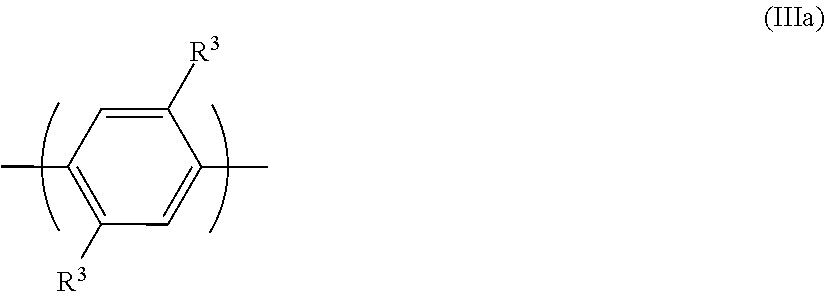
- a particularly preferred repeat unit of formula (III) has formula (IIIa):
- Substituents R 3 of formula (IIIa) are adjacent to linking positions of the repeat unit, which may cause steric hindrance between the repeat unit of formula (IIIa) and adjacent repeat units, resulting in the repeat unit of formula (IIIa) twisting out of plane relative to one or both adjacent repeat units.
- Exemplary repeat units where n is 2 or 3 include the following:
- a preferred repeat unit has formula (IIIb):
- the two R 3 groups of formula (IIIb) may cause steric hindrance between the phenyl rings they are bound to, resulting in twisting of the two phenyl rings relative to one another.
- a further class of arylene repeat units is optionally substituted fluorene repeat units, such as repeat units of formula (IV):
- R 3 in each occurrence is the same or different and is a substituent as described with reference to formula (III), and wherein the two groups R 3 may be linked to form a ring; R 8 is a substituent; and d is 0, 1, 2 or 3.
- the aromatic carbon atoms of the fluorene repeat unit may be unsubstituted, or may be substituted with one or more substituents R 8 .
- substituents R 8 are alkyl, for example C 1-20 alkyl, wherein one or more non-adjacent C atoms may be replaced with O, S, NH or substituted N, C ⁇ O and —COO—, optionally substituted aryl, optionally substituted heteroaryl, alkoxy, alkylthio, fluorine, cyano and arylalkyl.
- Particularly preferred substituents include C 1-20 alkyl and substituted or unsubstituted aryl, for example phenyl.
- Optional substituents for the aryl include one or more C 1-20 alkyl groups.
- Substituted N may be —NR S — wherein R 5 is C 1-20 alkyl; unsubstituted phenyl; or phenyl substituted with one or more C 1-20 alkyl groups.
- the extent of conjugation of repeat units of formula (IV) to aryl or heteroaryl groups of adjacent repeat units may be controlled by (a) linking the repeat unit through the 3- and/or 6-positions to limit the extent of conjugation across the repeat unit, and/or (b) substituting the repeat unit with one or more substituents R 8 in or more positions adjacent to the linking positions in order to create a twist with the adjacent repeat unit or units, for example a 2,7-linked fluorene carrying a C 1-20 alkyl substituent in one or both of the 3-and 6-positions.
- the repeat unit of formula (IV) may be an optionally substituted 2,7-linked repeat unit of formula (IVa):
- the repeat unit of formula (IVa) is not substituted in a position adjacent to the 2- or 7-position.
- Linkage through the 2- and 7-positions and absence of substituents adjacent to these linking positions provides a repeat unit that is capable of providing a relatively high degree of conjugation across the repeat unit.
- the repeat unit of formula (IV) may be an optionally substituted 3,6-linked repeat unit of formula (IVb)
- the extent of conjugation across a repeat unit of formula (IVb) may be relatively low as compared to a repeat unit of formula (IVa).
- Another exemplary arylene repeat unit has formula (V):
- R 3 , R 8 and d are as described with reference to formula (III) and (IV) above. Any of the R 3 groups may be linked to any other of the R 3 groups to form a substituted or unsubstituted ring. Aromatic carbon atoms of the repeat unit of formula (V) may be unsubstituted, or may be substituted with one or more substituents.
- Repeat units of formula (V) may have formula (Va) or (Vb):
- the host polymer may contain triazine-containing repeat units.
- Exemplary triazine-containing repeat units have formula (VIII):
- Ar 8 , Ar 9 and Ar 10 are independently selected from substituted or unsubstituted aryl or heteroaryl, and z in each occurrence is independently at least 1, optionally 1, 2 or 3, preferably 1.
- any of Ar 8 , Ar 9 and, if present, Ar 10 may be substituted with one or more substituents.
- substituents R 10 are substituents R 10 , wherein each R 10 may independently be selected from the group consisting of:
- Ar 8 , Ar 9 and Ar 10 of formula (VIII) are each phenyl, each phenyl independently being unsubstituted or substituted with one or more C 1-20 alkyl groups.
- Ar 10 of formula (VIII) is preferably phenyl, and is optionally substituted with one or more C 1-20 alkyl groups or a crosslinkable unit.
- a particularly preferred repeat unit of formula (VIII) has formula (VIIIa), which may be unsubstituted or substituted with one or more substituents R 10 , preferably one or more C 1-20 alkyl groups:
- Exemplary conjugation-breaking repeat units include repeat units of formula —(Ar 7 -Sp 1 -Ar 7 )— (IX) wherein Ar 7 independently in each occurrence represents an aromatic or heteroaromatic group that may be unsubstituted or substituted with one or more substituents, and Sp 1 represents a spacer group comprising at least one sp 3 hybridised carbon atom separating the two groups Ar 7 .
- each Ar 7 is phenyl and Sp 1 is a spacer group and containing at least one sp 3 -hybridised carbon atom spacing the two groups Ar 7 from each other, optionally a C 1-10 alkyl group wherein one or more non-adjacent C atoms of the C 1-10 alkyl group may be replaced with O, S, C ⁇ O or COO.
- Substituents for Ar 7 may be selected from groups R 1 described above with reference to formula (III), and are preferably selected from C 1-20 alkyl.
- the hole-transporting material of the emissive hole-transporting layer 205 may be a non-polymeric or polymeric material.
- Exemplary hole transporting materials may have a electron affinity of ⁇ 2.9 eV or lower (i.e. closer to vacuum level) and an ionisation potential of ⁇ 5.8 eV or lower, preferably ⁇ 5.7 eV or lower.
- Hole-transporting polymers include conjugated and non-conjugated polymers.
- a conjugated hole-transporting polymer may comprise repeat units of formula (VII):
- Ar 8 and Ar 9 in each occurrence are independently selected from substituted or unsubstituted aryl or heteroaryl, g is greater than or equal to 1, preferably 1 or 2, R 13 is H or a substituent, preferably a substituent, and c and d are each independently 1, 2 or 3.
- R 13 which may be the same or different in each occurrence when g>1, is preferably selected from the group consisting of alkyl, for example C 1-20 alkyl, Ar 10 , a branched or linear chain of Ar 10 groups, or a crosslinkable unit that is bound directly to the N atom of formula (VII) or spaced apart therefrom by a spacer group, wherein Ar 10 in each occurrence is independently optionally substituted aryl or heteroaryl.
- Exemplary spacer groups are C 1-20 alkyl, phenyl and phenyl-C 1-20 alkyl.
- Ar 8 , Ar 9 and, if present, Ar 10 in the repeat unit of Formula (VII) may be linked by a direct bond or a divalent linking atom or group to another of Ar 8 , Ar 9 and Ar 10 .
- Preferred divalent linking atoms and groups include O, S; substituted N; and substituted C.
- Preferred repeat units of formula (VII) have formulae 1-3:
- R 13 is Ar 10 and each of Ar 8 , Ar 9 and Ar 10 are independently and optionally substituted with one or more C 1-20 alkyl groups.
- Ar 8 , Ar 9 and Ar 10 are preferably phenyl.
- the central Ar 9 group of formula (1) linked to two N atoms is a polycyclic aromatic that may be unsubstituted or substituted with one or more substituents R 10 .
- exemplary polycyclic aromatic groups are naphthalene, perylene, anthracene and fluorene.
- Ar 8 and Ar 9 are phenyl, each of which may be substituted with one or more C 1-20 alkyl groups, and R 13 is —(Ar 10 ) r wherein r is at least 2 and wherein the group —(Ar 10 ) r forms a linear or branched chain of aromatic or heteroaromatic groups, for example 3,5-diphenylbenzene wherein each phenyl may be substituted with one or more C 1-20 alkyl groups.
- c, d and g are each 1 and Ar 8 and Ar 9 are phenyl linked by an oxygen atom to form a phenoxazine ring.
- a hole-transporting polymer comprising repeat units of formula (VII) may be a homopolymer or a copolymer containing repeat units of formula (VII) and one or more co-repeat units.
- exemplary co-repeat units include arylene repeat units that may be unsubstituted or substituted with one or more substituents, for example one or more C 1-40 hydrocarbyl groups.
- Exemplary arylene repeat units include repeat units (III), (IV) and (V) described above.
- repeat units of formula (VII) may be provided in a molar amount in the range of about 10 mol % up to about 95 mol %, optionally about 10-75 mol % or about 10-50 mol %.
- the hole-transporting polymer may contain one, two or more different repeat units of formula (VII).
- the hole-transporting polymer may contain crosslinkable groups that may be crosslinked following deposition of the hole-transporting polymer to form an insoluble, crosslinked hole-transporting layer prior to formation of the second light-emitting layer.
- Crosslinkable groups may be provided as substituents of any repeat units of the polymer, for example any of repeat units (III), (IV), (V) or (VII) that may be present in the hole-transporting polymer.
- Charge-transporting and/or light-emitting polymers as described anywhere herein are suitably amorphous polymers.
- Phosphorescent materials of the emissive hole-transporting layer 205 and the second light-emitting layer 207 may be selected from phosphorescent transition metal complexes, with the proviso that the phosphorescent material of the hole-transporting layer 205 has a triplet energy level that is lower than the triplet energy level of a phosphorescent material in the second light-emitting layer 207 .
- Exemplary phosphorescent transition metal complexes have formula (IX): ML 1 q L 2 r L 3 s (IX) wherein M is a metal; each of L 1 , L 2 and L 3 is a coordinating group; q is a positive integer; r and s are each independently 0 or a positive integer; and the sum of (a. q)+(b. r)+(c.s) is equal to the number of coordination sites available on M, wherein a is the number of coordination sites on L 1 , b is the number of coordination sites on L 2 and c is the number of coordination sites on L 3 .
- Heavy elements M induce strong spin-orbit coupling to allow rapid intersystem crossing and emission from triplet or higher states.
- Suitable heavy metals M include d-block metals, in particular those in rows 2 and 3 i.e. elements 39 to 48 and 72 to 80, in particular ruthenium, rhodium, palladium, rhenium, osmium, iridium, platinum and gold. Iridium is particularly preferred.
- Exemplary ligands L 1 , L 2 and L 3 include carbon or nitrogen donors such as porphyrin or bidentate ligands of formula (X):
- Ar 5 and Ar 6 may be the same or different and are independently selected from substituted or unsubstituted aryl or heteroaryl; X 1 and Y 1 may be the same or different and are independently selected from carbon or nitrogen; and Ar 5 and Ar 6 may be fused together.
- Ligands wherein X 1 is carbon and Y 1 is nitrogen are preferred, in particular ligands in which Ar 5 is a single ring or fused heteroaromatic of N and C atoms only, for example pyridyl or isoquinoline, and Ar 6 is a single ring or fused aromatic, for example phenyl or naphthyl.
- Ar 5 may be selected from phenyl, fluorene, naphthyl and Ar 6 are selected from quinoline, isoquinoline, thiophene and benzothiophene.
- Ar 5 may be selected from phenyl or fluorene and Ar 6 may be pyridine.
- Ar 5 may be selected from phenyl and Ar 6 may be selected from imidazole, pyrazole, triazole and tetrazole.
- Each of Ar y and Ar 6 may carry one or more substituents. Two or more of these substituents may be linked to form a ring, for example an aromatic ring.
- ligands suitable for use with d-block elements include diketonates, in particular acetylacetonate (acac), tetrakis-(pyrazol-1-yl)borate, 2-carboxypyridyl, triarylphosphines and pyridine, each of which may be substituted.
- diketonates in particular acetylacetonate (acac), tetrakis-(pyrazol-1-yl)borate, 2-carboxypyridyl, triarylphosphines and pyridine, each of which may be substituted.
- substituents include groups R 13 as described above with reference to Formula (VII). Particularly preferred substituents include fluorine or trifluoromethyl which may be used to blue-shift the emission of the complex, for example as disclosed in WO 02/45466, WO 02/44189, US 2002-117662 and US 2002-182441; alkyl or alkoxy groups, for example C 1-20 alkyl or alkoxy, which may be as disclosed in JP 2002-324679; carbazole which may be used to assist hole transport to the complex when used as an emissive material, for example as disclosed in WO 02/81448; and dendrons which may be used to obtain or enhance solution processability of the metal complex, for example as disclosed in WO 02/66552.
- substituents include fluorine or trifluoromethyl which may be used to blue-shift the emission of the complex, for example as disclosed in WO 02/45466, WO 02/44189, US 2002-117662 and US 2002-182441; alkyl or alkoxy groups, for example
- a light-emitting dendrimer typically comprises a light-emitting core bound to one or more dendrons, wherein each dendron comprises a branching point and two or more dendritic branches.
- the dendron is at least partially conjugated, and at least one of the branching points and dendritic branches comprises an aryl or heteroaryl group, for example a phenyl group.
- the branching point group and the branching groups are all phenyl, and each phenyl may independently be substituted with one or more substituents, for example alkyl or alkoxy.
- a dendron may have optionally substituted formula (XI)
- BP represents a branching point for attachment to a core and G 1 represents first generation branching groups.
- the dendron may be a first, second, third or higher generation dendron.
- G 1 may be substituted with two or more second generation branching groups G 2 , and so on, as in optionally substituted formula (XIa):
- each of BP and G 1 , G 2 . . . G n is phenyl, and each phenyl BP, G 1 , G 2 . . . G n-1 is a 3,5-linked phenyl.
- a preferred dendron is a substituted or unsubstituted dendron of formula (XIb):
- BP and/or any group G may be substituted with one or more substituents, for example one or more C 1-20 alkyl or alkoxy groups.
- the phosphorescent material of the hole-transporting layer may be covalently bound to the hole-transporting material or it may be mixed with the hole-transporting material.
- the or each phosphorescent material of the second light-emitting layer may be covalently bound to a host material of the second light-emitting layer or may be mixed with the host material.
- the phosphorescent material may be a repeat unit in the polymer backbone, provided as an end-group of the polymer, or provided in a side-chain of the polymer. If the phosphorescent material is provided as a side-chain then it may be directly bound to a repeat unit in the backbone of the polymer or it may be spaced apart from the polymer backbone by a spacer group.
- Exemplary spacer groups include C 1-20 alkyl and aryl-C 1-20 alkyl, for example phenyl-C 1-20 alkyl.
- One or more carbon atoms of an alkyl group of a spacer group may be replaced with O, S, C ⁇ O or COO.
- a phosphorescent material of the hole-transporting layer or the second light-emitting layer, and optional spacer may be provided as a substituent R 3 of any of repeat units of formulae (III), (IV) or (V) described above that may be present in a hole-transporting polymer or host polymer, respectively.
- Covalent binding of the phosphorescent material to the hole-transporting material may reduce or avoid washing of the phosphorescent material out of the hole-transporting layer if an overlying light-emitting layer is deposited from a formulation of the light-emitting layer materials in a solvent or solvent mixture.
- the phosphorescent material may be provided in an amount in the range of 0.1-20 weight %, optionally 0.1-5 mol % of the hole-transporting material/phosphorescent material mixture.
- repeat units comprising the phosphorescent material, or an end unit comprising the phosphorescent material may form 0.1-20 mol %, optionally 0.1-5 mol % of the polymer.
- the or each phosphorescent material may be provided in an amount in the range of 0.1-50 weight % of the host and phosphorescent emitter(s).
- a blue phosphorescent material may be provided in an amount in the range of 10-50 weight % of the host and phosphorescent emitter(s).
- a green phosphorescent material may be provided in an amount in the range of 0.1-10 weight % of the host and phosphorescent emitter(s).
- repeat units comprising the phosphorescent material, or an end unit comprising the phosphorescent material may form 0.1-50 mol of the polymer.
- the phosphorescent material with the highest triplet energy level is preferably provided in a larger weight percentage than the lower triplet energy level material or materials.
- HOMO and LUMO levels as described anywhere herein may be measured by square wave voltammetry.
- the working electrode potential may be ramped linearly versus time. When cyclic voltammetry reaches a set potential the working electrode's potential ramp is inverted. This inversion can happen multiple times during a single experiment.
- the current at the working electrode is plotted versus the applied voltage to give the cyclic voltammogram trace.
- Apparatus to measure HOMO or LUMO energy levels by CV may comprise a cell containing a tert-butyl ammonium perchlorate/ or tertbutyl ammonium hexafluorophosphate solution in acetonitrile, a glassy carbon working electrode where the sample is coated as a film, a platinum counter electrode (donor or acceptor of electrons) and a reference glass electrode no leak Ag/AgCl. Ferrocene is added in the cell at the end of the experiment for calculation purposes.
- a good reversible reduction event is typically observed for thick films measured at 200 mV/s and a switching potential of ⁇ 2.5V.
- the reduction events should be measured and compared over 10 cycles, usually measurements are taken on the 3 rd cycle. The onset is taken at the intersection of lines of best fit at the steepest part of the reduction event and the baseline.
- HOMO and LUMO values may be measured at ambient temperature.
- a conductive hole injection layer which may be formed from a conductive organic or inorganic material, may be provided between the anode 203 and the emissive hole-transporting layer 205 .
- conductive organic materials include optionally substituted, doped poly(ethylene dioxythiophene) (PEDT), in particular PEDT doped with a charge-balancing polyacid such as polystyrene sulfonate (PSS) as disclosed in EP 0901176 and EP 0947123, polyacrylic acid or a fluorinated sulfonic acid, for example Nafion®; polyaniline as disclosed in U.S. Pat. No. 5,723,873 and U.S. Pat. No.
- PES polystyrene sulfonate
- conductive inorganic materials include transition metal oxides such as VOx, MoOx and RuOx as disclosed in Journal of Physics D: Applied Physics (1996), 29(11), 2750-2753.
- the cathode 209 is selected from materials that have a workfunction allowing injection of electrons into the second light-emitting layer 207 of the OLED. Other factors influence the selection of the cathode such as the possibility of adverse interactions between the cathode and the light-emitting material.
- the cathode may consist of a single material such as a layer of aluminium. Alternatively, it may comprise a plurality of conductive materials such as metals, for example a bilayer of a low workfunction material and a high workfunction material such as calcium and aluminium, for example as disclosed in WO 98/10621.
- the cathode may comprise elemental barium, for example as disclosed in WO 98/57381, Appl. Phys. Lett.
- the cathode may comprise a thin layer of metal compound, in particular an oxide or fluoride of an alkali or alkali earth metal, between the organic layers of the device and one or more conductive cathode layers to assist electron injection, for example lithium fluoride as disclosed in WO 00/48258; barium fluoride as disclosed in Appl. Phys. Lett. 2001, 79(5), 2001; and barium oxide.
- the cathode preferably has a workfunction of less than 3.5 eV, more preferably less than 3.2 eV, most preferably less than 3 eV. Work functions of metals can be found in, for example, Michaelson, J. Appl. Phys. 48(11), 4729, 1977.
- the cathode may be opaque or transparent.
- Transparent cathodes are particularly advantageous for active matrix devices because emission through a transparent anode in such devices is at least partially blocked by drive circuitry located underneath the emissive pixels.
- a transparent cathode comprises a layer of an electron injecting material that is sufficiently thin to be transparent. Typically, the lateral conductivity of this layer will be low as a result of its thinness. In this case, the layer of electron injecting material is used in combination with a thicker layer of transparent conducting material such as indium tin oxide.
- a transparent cathode device need not have a transparent anode (unless, of course, a fully transparent device is desired), and so the transparent anode used for bottom-emitting devices may be replaced or supplemented with a layer of reflective material such as a layer of aluminium.
- transparent cathode devices are disclosed in, for example, GB 2348316.
- the substrate preferably has good barrier properties for prevention of ingress of moisture and oxygen into the device.
- the substrate is commonly glass, however alternative substrates may be used, in particular where flexibility of the device is desirable.
- the substrate may comprise one or more plastic layers, for example a substrate of alternating plastic and dielectric barrier layers or a laminate of thin glass and plastic.
- the device may be encapsulated with an encapsulant (not shown) to prevent ingress of moisture and oxygen.
- encapsulants include a sheet of glass, films having suitable barrier properties such as silicon dioxide, silicon monoxide, silicon nitride or alternating stacks of polymer and dielectric or an airtight container.
- a transparent encapsulating layer such as silicon monoxide or silicon dioxide may be deposited to micron levels of thickness, although in one preferred embodiment the thickness of such a layer is in the range of 20-300 nm.
- a getter material for absorption of any atmospheric moisture and/or oxygen that may permeate through the substrate or encapsulant may be disposed between the substrate and the encapsulant.
- a formulation suitable for forming the emissive hole-transporting layer or the second light-emitting layer may be formed from the components forming those layers and one or more suitable solvents.
- the formulation may be a solution of the polymer and any other components in the one or more solvents, or may be a dispersion in the one or more solvents in which one or more components are not dissolved.
- the formulation is a solution.
- Exemplary solvents include benzenes substituted with one or more substituents selected from C 1-10 alkyl and C 1-10 alkoxy groups, for example toluene, xylenes and methylanisoles.
- Particularly preferred solution deposition techniques including printing and coating techniques such spin-coating and inkjet printing.
- Coating methods are particularly suitable for devices wherein patterning of the light-emitting layer is unnecessary—for example for lighting applications or simple monochrome segmented displays.
- a device may be inkjet printed by providing a patterned layer over the anode and defining wells for printing of one colour (in the case of a monochrome device) or multiple colours (in the case of a multicolour, in particular full colour device).
- the patterned layer is typically a layer of photoresist that is patterned to define wells as described in, for example, EP 0880303.
- the ink may be printed into channels defined within a patterned layer.
- the photoresist may be patterned to form channels which, unlike wells, extend over a plurality of pixels and which may be closed or open at the channel ends.
- solution deposition techniques include dip-coating, roll printing and screen printing.
- Phosphorescent materials of the light-emitting layer were selected from the following monomers:
- ITO is an indium-tin oxide anode
- HIL is a hole-injecting layer
- HTL is a hole-transporting layer (that may or may not be emissive)
- LE is a light-emitting layer.
- a substrate carrying ITO was cleaned using UV/Ozone.
- the hole injection layer was formed by spin-coating an aqueous formulation of a hole-injection material available from Plextronics, Inc.
- a hole transporting layer was formed to a thickness of 22 nm by spin-coating a hole-transporting polymer (that may or may not be emissive) and crosslinking the polymer by heating.
- a light-emitting layer was formed to a thickness of 75 nm by spin-coating a light-emitting composition of a host polymer and phosphorescent light-emitting compounds.
- a cathode was formed by evaporation of a first layer of a metal fluoride to a thickness of about 2 nm, a second layer of aluminium to a thickness of about 200 nm and an optional third layer of silver.
- devices containing a non-emissive hole-transporting layer and a white light-emitting layer were prepared.
- a high triplet energy hole-transporting polymer (High T1 HTM) was used; in another example, a low triplet energy hole-transporting polymer (Low T1 HTM) was used.
- High T1 HTM was prepared by Suzuki polymerisation as described in WO 00/53656 of the following monomers:
- the lowest excited state triplet energy level of the High T1 HTM is 2.52 eV.
- the lowest excited state triplet energy level of the Low T1 HTM is 2.17 eV.
- the T1 values of the hole-transporting polymers were measured by low temperature phosophorescence spectroscopy.
- Two devices were prepared according to the General Device Process—one in which the hole-transporting layer was formed Low T1 HTM, and one in which the hole-transporting layer was formed using High T1 HTM.
- the light-emitting layer of both devices was formed from a composition as set out in Table 1.
- the monomers listed for Host Polymer 1 in Table 1 are the monomers used to form the polymer by Suzuki polymerisation as described in WO 00/53636. LUMO levels were measured by square wave voltammetry.
- the device containing the Low T1 HTM has higher conductivity, which is attributed to the greater degree of conjugation of the Low T1 HTM.
- the half-life of the devices containing the Low T1 HTM (dotted lines) is also much longer than devices containing the High T1 HTM (solid lines) (“half-life” as used herein means the time taken for luminance of a device to fall to 50% of a starting brightness).
- devices containing the Low T1 HTM suffers from significantly worse efficiency than devices containing the High T1 HTM (solid lines), which is attributed to quenching of phosphorescence by the Low T1 HTM.
- a device having a hole-transporting layer formed from a phosphorescent red emitting, low triplet energy hole-transporting polymer and a light-emitting layer containing green and blue phosphorescent materials was formed according to the General Device Process.
- a comparative device having a hole-transporting layer formed from a non-emissive, low triplet energy hole-transporting polymer and a light-emitting layer containing red, green and blue phosphorescent materials was prepared according to the General Device Process.
- the hole-transporting polymers used to form the hole-transporting layers of the comparative and exemplary devices were formed by Suzuki polymerisation as described in WO 00/53656 of monomers are set out in Table 2.
- the light-emitting layers of the exemplary device and the comparative device were formed from Host Polymer 2 doped with phosphorescent materials as set out in Table 3.
- Host Polymer 2 was formed by Suzuki polymerisation as described in WO 00/53656 of the following monomers:
- the electroluminescent spectra and conductivities of the exemplary device and the comparative device are similar.
- the external quantum efficiencies of the exemplary devices are higher than those of the comparative device (solid lines).
- the comparative device solid lines.
- the presence of a phosphorescent material in the low triplet energy hole-transporting layer of this example provides both longer lifetime and higher efficiency than a device in which all phosphorescent materials are provided in a single layer.
Abstract
- the first light-emitting layer comprises a hole-transporting material and a first phosphorescent material,
- the second light-emitting layer comprises a second phosphorescent material; and
- the lowest triplet excited state energy level of the hole-transporting material is: (a) lower than the lowest triplet excited state of the second phosphorescent material, and (b) the same as or higher than the lowest triplet excited state energy level of the first phosphorescent material.
Description
- the first light-emitting layer comprises a hole-transporting material and a first phosphorescent material,
- the second light-emitting layer comprises a second phosphorescent material; and
- the lowest triplet excited state energy level of the hole-transporting material is: (a) lower than the lowest triplet excited state of the second phosphorescent material, and (b) the same as or higher than the lowest triplet excited state energy level of the first phosphorescent material.

wherein q in each occurrence is independently 0, 1, 2, 3 or 4, optionally 1 or 2; n is 1, 2 or 3; and R3 independently in each occurrence is a substituent.
-
- alkyl, optionally C1-20 alkyl, wherein one or more non-adjacent C atoms may be replaced with optionally substituted aryl or heteroaryl, O, S, substituted N, C═O or —COO—, and one or more H atoms may be replaced with F;
- aryl and heteroaryl groups that may be unsubstituted or substituted with one or more substituents, preferably phenyl substituted with one or more C1-20 alkyl groups;
- a linear or branched chain of aryl or heteroaryl groups, each of which groups may independently be substituted, for example a group of formula —(Ar3)r wherein each Ar3 is independently an aryl or heteroaryl group and r is at least 2, preferably a branched or linear chain of phenyl groups each of which may be unsubstituted or substituted with one or more C1-20 alkyl groups; and
- a crosslinkable-group, for example a group comprising a double bond such and a vinyl or acrylate group, or a benzocyclobutane group.
-
- alkyl, for example C1-20 alkyl, wherein one or more non-adjacent C atoms may be replaced with O, S, substituted N, C═O and —COO— and one or more H atoms of the alkyl group may be replaced with F;
- NR9 2, OR9, SR9, SiR9 3 and
- fluorine, nitro and cyano;
wherein each R9 is independently selected from the group consisting of alkyl, preferably C1-20 alkyl; and aryl or heteroaryl, preferably phenyl, optionally substituted with one or more C1-20 alkyl groups.


wherein R3 in each occurrence is the same or different and is a substituent as described with reference to formula (III), and wherein the two groups R3 may be linked to form a ring; R8 is a substituent; and d is 0, 1, 2 or 3.


wherein R3, R8 and d are as described with reference to formula (III) and (IV) above. Any of the R3 groups may be linked to any other of the R3 groups to form a substituted or unsubstituted ring. Aromatic carbon atoms of the repeat unit of formula (V) may be unsubstituted, or may be substituted with one or more substituents.


wherein Ar8, Ar9 and Ar10 are independently selected from substituted or unsubstituted aryl or heteroaryl, and z in each occurrence is independently at least 1, optionally 1, 2 or 3, preferably 1.
-
- substituted or unsubstituted alkyl, optionally C1-20 alkyl, wherein one or more non-adjacent C atoms may be replaced with optionally substituted aryl or heteroaryl, O, S, substituted N, C═O or —COO— and one or more H atoms may be replaced with F; and
- a crosslinkable group attached directly to Ar8, Ar9 or Ar10 or spaced apart therefrom by a spacer group, for example a group comprising a double bond such and a vinyl or acrylate group, or a benzocyclobutane group.

—(Ar7-Sp1-Ar7)— (IX)
wherein Ar7 independently in each occurrence represents an aromatic or heteroaromatic group that may be unsubstituted or substituted with one or more substituents, and Sp1 represents a spacer group comprising at least one sp3 hybridised carbon atom separating the two groups Ar7. Preferably, each Ar7 is phenyl and Sp1 is a spacer group and containing at least one sp3-hybridised carbon atom spacing the two groups Ar7 from each other, optionally a C1-10 alkyl group wherein one or more non-adjacent C atoms of the C1-10alkyl group may be replaced with O, S, C═O or COO. Substituents for Ar7 may be selected from groups R1 described above with reference to formula (III), and are preferably selected from C1-20 alkyl.
Hole-Transporting Material

wherein Ar8 and Ar9 in each occurrence are independently selected from substituted or unsubstituted aryl or heteroaryl, g is greater than or equal to 1, preferably 1 or 2, R13 is H or a substituent, preferably a substituent, and c and d are each independently 1, 2 or 3.

ML1 qL2 rL3 s (IX)
wherein M is a metal; each of L1, L2 and L3 is a coordinating group; q is a positive integer; r and s are each independently 0 or a positive integer; and the sum of (a. q)+(b. r)+(c.s) is equal to the number of coordination sites available on M, wherein a is the number of coordination sites on L1, b is the number of coordination sites on L2 and c is the number of coordination sites on L3.

wherein Ar5 and Ar6 may be the same or different and are independently selected from substituted or unsubstituted aryl or heteroaryl; X1 and Y1 may be the same or different and are independently selected from carbon or nitrogen; and Ar5 and Ar6 may be fused together. Ligands wherein X1 is carbon and Y1 is nitrogen are preferred, in particular ligands in which Ar5 is a single ring or fused heteroaromatic of N and C atoms only, for example pyridyl or isoquinoline, and Ar6 is a single ring or fused aromatic, for example phenyl or naphthyl.


wherein BP represents a branching point for attachment to a core and G1 represents first generation branching groups.

wherein u is 0 or 1; v is 0 if u is 0 or may be 0 or 1 if u is 1; BP represents a branching point for attachment to a core and G1, G2 and G3 represent first, second and third generation dendron branching groups. In one preferred embodiment, each of BP and G1, G2 . . . Gn is phenyl, and each phenyl BP, G1, G2 . . . Gn-1 is a 3,5-linked phenyl.

wherein * represents an attachment point of the dendron to a core.
- 3 mm diameter glassy carbon working electrode
- Ag/AgCl/no leak reference electrode
- Pt wire auxiliary electrode
- 0.1M tetrabutylammonium hexafluorophosphate in acetonitrile
- LUMO=4.8−ferrocene(peak to peak maximum average)+onset
Sample: 1 drop of 5 mg/mL in toluene spun at 3000 rpm LUMO (reduction) measurement:


General Device Process
- ITO/HIL/HTL/LE/Cathode
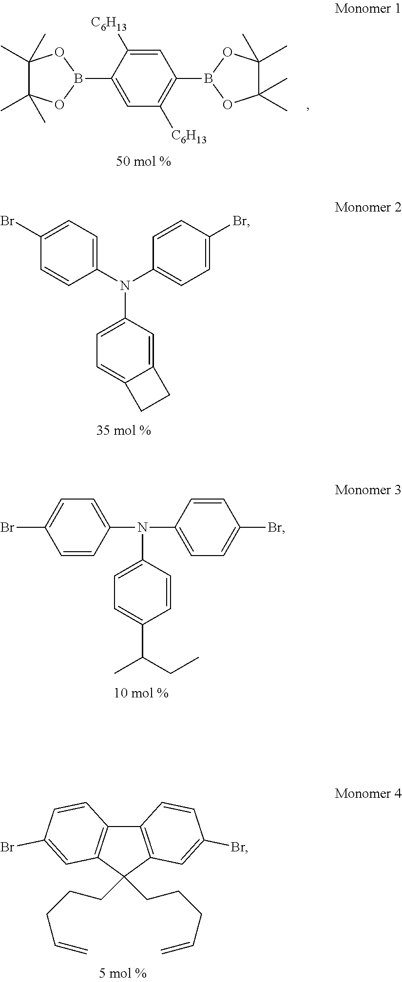

| TABLE 1 | ||
| Material | Weight ratio (%) | LUMO (eV) |
| |
||
| |
61.3 | −1.8 |
| |
||
| |
36.1 | −1.88 |
| |
1.5 | −2.2 |
| |
1.2 | −2.49 |
| TABLE 2 | ||
| Emissive Hole- | Non-Emissive Hole- | |
| Transporting Polymer | Transporting | |
| Monomer | ||
| 1, 50 | Monomer | 1, 50 |
| Monomer | ||
| 5, 36.516 | Monomer | 5, 36.516 |
| Monomer | ||
| 7, 10 | Monomer | 7, 10 |
| Monomer | ||
| 8, 3.484 | Monomer | 8, 2.884 mol % |
| Monomer 9, 1.2 mol % | — | |
| (Phosphorescent red end-capping group) | ||
- Monomer 10: 50 mol %
- Monomer 11: 25 mol %
- Monomer 12: 25 mol %
| TABLE 3 | |
| Exemplary Device | Comparative Device |
| Weight | LUMO | Weight | ||
| Material | % | (eV) | Material | |
| Host Polymer |
| 2 | 54 | −2.6 | |
53.7 |
| |
45 | −1.88 | |
45 |
| |
1 | −2.2 | |
1 |
| |
0 | −2.49 | |
0.3 |
Claims (17)
Applications Claiming Priority (2)
| Application Number | Priority Date | Filing Date | Title |
|---|---|---|---|
| GB1310036.7 | 2013-06-05 | ||
| GB1310036.7A GB2514818B (en) | 2013-06-05 | 2013-06-05 | Polymer and organic electronic device |
Publications (2)
| Publication Number | Publication Date |
|---|---|
| US20140361274A1 US20140361274A1 (en) | 2014-12-11 |
| US9099666B2 true US9099666B2 (en) | 2015-08-04 |
Family
ID=48805793
Family Applications (1)
| Application Number | Title | Priority Date | Filing Date |
|---|---|---|---|
| US14/296,682 Active US9099666B2 (en) | 2013-06-05 | 2014-06-05 | Organic light-emitting device |
Country Status (5)
| Country | Link |
|---|---|
| US (1) | US9099666B2 (en) |
| EP (1) | EP2811524A1 (en) |
| JP (1) | JP6636234B2 (en) |
| CN (1) | CN104241539B (en) |
| GB (1) | GB2514818B (en) |
Cited By (1)
| Publication number | Priority date | Publication date | Assignee | Title |
|---|---|---|---|---|
| WO2017051147A1 (en) * | 2015-09-22 | 2017-03-30 | Cambridge Display Technology Limited | An organic light emitting device which emits white light |
Families Citing this family (8)
| Publication number | Priority date | Publication date | Assignee | Title |
|---|---|---|---|---|
| JP5905916B2 (en) * | 2013-12-26 | 2016-04-20 | 出光興産株式会社 | Organic electroluminescence device and electronic device |
| CN106415872B (en) * | 2014-04-25 | 2019-05-28 | 住友化学株式会社 | Light-emitting component |
| JP5867580B2 (en) | 2014-06-04 | 2016-02-24 | 住友化学株式会社 | Light emitting element |
| GB2530746A (en) * | 2014-09-30 | 2016-04-06 | Cambridge Display Tech Ltd | Organic Light Emitting Device |
| GB2530748A (en) * | 2014-09-30 | 2016-04-06 | Cambridge Display Tech Ltd | Organic Light Emitting Device |
| US10020458B2 (en) | 2014-12-18 | 2018-07-10 | Lg Display Co., Ltd. | White organic light-emitting display device |
| CN104538554B (en) * | 2015-01-13 | 2017-01-25 | 北京科技大学 | Organic light-emitting diode with double-component-mixed electron-transport/hole barrier layer |
| JP6596918B2 (en) * | 2015-05-19 | 2019-10-30 | 住友化学株式会社 | Light emitting element |
Citations (2)
| Publication number | Priority date | Publication date | Assignee | Title |
|---|---|---|---|---|
| EP1175128A2 (en) | 2000-07-17 | 2002-01-23 | Fuji Photo Film Co., Ltd. | Light emitting element and azole compound |
| US20080145520A1 (en) | 2006-12-04 | 2008-06-19 | Asahi Kasei Kabushiki Kaisha | Method for producing electronic device and coating solutions suitable for the production method |
Family Cites Families (42)
| Publication number | Priority date | Publication date | Assignee | Title |
|---|---|---|---|---|
| US5723873A (en) | 1994-03-03 | 1998-03-03 | Yang; Yang | Bilayer composite electrodes for diodes |
| US5798170A (en) | 1996-02-29 | 1998-08-25 | Uniax Corporation | Long operating life for polymer light-emitting diodes |
| WO1998005187A1 (en) | 1996-07-29 | 1998-02-05 | Cambridge Display Technology Limited | Electroluminescent devices with electrode protection |
| DE69724129T2 (en) | 1996-09-04 | 2004-02-26 | Cambridge Display Technology Ltd. | LIGHT-EMITTING ORGANIC DEVICES WITH IMPROVED CATHODE |
| JP3899566B2 (en) | 1996-11-25 | 2007-03-28 | セイコーエプソン株式会社 | Manufacturing method of organic EL display device |
| US6452218B1 (en) | 1997-06-10 | 2002-09-17 | Uniax Corporation | Ultra-thin alkaline earth metals as stable electron-injecting electrodes for polymer light emitting diodes |
| GB9718393D0 (en) | 1997-08-29 | 1997-11-05 | Cambridge Display Tech Ltd | Electroluminescent Device |
| GB9903251D0 (en) | 1999-02-12 | 1999-04-07 | Cambridge Display Tech Ltd | Opto-electric devices |
| WO2000053656A1 (en) | 1999-03-05 | 2000-09-14 | Cambridge Display Technology Limited | Polymer preparation |
| WO2000053636A2 (en) | 1999-03-08 | 2000-09-14 | Ceptyr, Inc. | Dsp-1 dual-specificity map kinase phosphatase |
| GB2348316A (en) | 1999-03-26 | 2000-09-27 | Cambridge Display Tech Ltd | Organic opto-electronic device |
| TW518768B (en) * | 2000-05-22 | 2003-01-21 | Showa Denko Kk | Organic electroluminescent device and light-emitting material |
| US6645645B1 (en) * | 2000-05-30 | 2003-11-11 | The Trustees Of Princeton University | Phosphorescent organic light emitting devices |
| US6939624B2 (en) | 2000-08-11 | 2005-09-06 | Universal Display Corporation | Organometallic compounds and emission-shifting organic electrophosphorescence |
| KR100750756B1 (en) | 2000-11-30 | 2007-08-20 | 캐논 가부시끼가이샤 | Luminescent Element and Display |
| AU2002222565A1 (en) | 2000-11-30 | 2002-06-11 | Canon Kabushiki Kaisha | Luminescent element and display |
| US6693295B2 (en) | 2000-12-25 | 2004-02-17 | Fuji Photo Film Co., Ltd. | Indole derivative, material for light-emitting device and light-emitting device using the same |
| EP1366113B1 (en) | 2001-02-20 | 2011-04-13 | Isis Innovation Limited | Metal-containing dendrimers |
| WO2002074015A2 (en) * | 2001-03-14 | 2002-09-19 | The Trustees Of Princeton University | Materials and devices for blue phosphorescence based organic light emitting diodes |
| CA2442904A1 (en) | 2001-04-05 | 2002-10-17 | Sankyo Company, Limited | Benzamidine derivative |
| JP2004519830A (en) | 2001-04-17 | 2004-07-02 | コーニンクレッカ フィリップス エレクトロニクス エヌ ヴィ | LED with conductive transparent polymer layer containing low sulfate and high metal ions |
| JP2002324679A (en) | 2001-04-26 | 2002-11-08 | Honda Motor Co Ltd | Organic electroluminescent element |
| KR100478524B1 (en) * | 2002-06-28 | 2005-03-28 | 삼성에스디아이 주식회사 | Electroluminescence display device using mixture of high molecular and low molecular emitting material as emitting material |
| TWI355661B (en) | 2003-12-18 | 2012-01-01 | Panasonic Corp | Method for using a variable-resistance material as |
| US7597967B2 (en) * | 2004-12-17 | 2009-10-06 | Eastman Kodak Company | Phosphorescent OLEDs with exciton blocking layer |
| TWI415920B (en) * | 2005-08-12 | 2013-11-21 | Sumitomo Chemical Co | High molecular weight material and element using such material |
| US9112170B2 (en) * | 2006-03-21 | 2015-08-18 | Semiconductor Energy Laboratory Co., Ltd. | Light-emitting element, light-emitting device, and electronic device |
| WO2009008359A1 (en) * | 2007-07-07 | 2009-01-15 | Idemitsu Kosan Co., Ltd. | Organic el device |
| WO2009008346A1 (en) * | 2007-07-07 | 2009-01-15 | Idemitsu Kosan Co., Ltd. | Organic el device |
| US8143613B2 (en) * | 2007-11-27 | 2012-03-27 | The Regents Of The University Of Michigan | Organic light emitting device having multiple separate emissive layers |
| GB2456787B (en) * | 2008-01-23 | 2010-06-02 | Cambridge Display Tech Ltd | Pulsed driven displays |
| JP2010031248A (en) * | 2008-06-23 | 2010-02-12 | Sumitomo Chemical Co Ltd | Composition and light-emitting element using the composition |
| KR20110018376A (en) * | 2008-06-23 | 2011-02-23 | 스미또모 가가꾸 가부시키가이샤 | Composition and light-emitting element using the composition |
| KR101352290B1 (en) * | 2008-09-30 | 2014-01-16 | 엘지디스플레이 주식회사 | Organic light emitting diodde desplay device |
| JP5457847B2 (en) * | 2009-01-23 | 2014-04-02 | ユー・ディー・シー アイルランド リミテッド | Organic electroluminescence device |
| GB0906554D0 (en) | 2009-04-16 | 2009-05-20 | Cambridge Display Tech Ltd | Organic electroluminescent device |
| JP2011093825A (en) * | 2009-10-28 | 2011-05-12 | Hodogaya Chem Co Ltd | Compound including 2,2-diphenyladamantyl structure, and organic electroluminescent element |
| CN102064282B (en) * | 2009-11-13 | 2013-06-12 | 昆山维信诺显示技术有限公司 | Organic electroluminescent device |
| JP6014304B2 (en) * | 2010-01-15 | 2016-10-25 | ユー・ディー・シー アイルランド リミテッド | Organic electroluminescence device |
| JPWO2011148909A1 (en) * | 2010-05-24 | 2013-07-25 | 出光興産株式会社 | Organic electroluminescence device |
| GB2485001A (en) | 2010-10-19 | 2012-05-02 | Cambridge Display Tech Ltd | OLEDs |
| GB201107917D0 (en) * | 2011-05-12 | 2011-06-22 | Cambridge Display Tech Ltd | Organic light emitting material and device |
-
2013
- 2013-06-05 GB GB1310036.7A patent/GB2514818B/en not_active Expired - Fee Related
-
2014
- 2014-05-29 EP EP14170510.3A patent/EP2811524A1/en not_active Withdrawn
- 2014-06-03 JP JP2014114483A patent/JP6636234B2/en active Active
- 2014-06-05 CN CN201410392024.6A patent/CN104241539B/en not_active Expired - Fee Related
- 2014-06-05 US US14/296,682 patent/US9099666B2/en active Active
Patent Citations (2)
| Publication number | Priority date | Publication date | Assignee | Title |
|---|---|---|---|---|
| EP1175128A2 (en) | 2000-07-17 | 2002-01-23 | Fuji Photo Film Co., Ltd. | Light emitting element and azole compound |
| US20080145520A1 (en) | 2006-12-04 | 2008-06-19 | Asahi Kasei Kabushiki Kaisha | Method for producing electronic device and coating solutions suitable for the production method |
Non-Patent Citations (3)
| Title |
|---|
| Extended European Search Report for European Application No. 14170510.3 dated Oct. 8, 2014. |
| Kimyonok et al., Norbornene-Based Copolymers with Iridium Complexes and Bis(carbazolyl)fluorene Groups in Their Side-Chains and Their Use in Light-Emitting Diodes. Chem Mater. 2007;19(23):5602-8. |
| Xiao et al., Recent progresses on materials for electrophosphorescent organic light-emitting devices. Adv Mater. Feb. 22, 2011;23(8):926-52. doi: 10.1002/adma.201003128. Epub Oct. 28, 2010. |
Cited By (2)
| Publication number | Priority date | Publication date | Assignee | Title |
|---|---|---|---|---|
| WO2017051147A1 (en) * | 2015-09-22 | 2017-03-30 | Cambridge Display Technology Limited | An organic light emitting device which emits white light |
| US10770686B2 (en) | 2015-09-22 | 2020-09-08 | Cambridge Display Technology Limited | Organic light emitting device which emits white light |
Also Published As
| Publication number | Publication date |
|---|---|
| EP2811524A1 (en) | 2014-12-10 |
| CN104241539A (en) | 2014-12-24 |
| GB2514818B (en) | 2015-12-16 |
| US20140361274A1 (en) | 2014-12-11 |
| GB201310036D0 (en) | 2013-07-17 |
| CN104241539B (en) | 2018-02-13 |
| JP6636234B2 (en) | 2020-01-29 |
| JP2014239219A (en) | 2014-12-18 |
| GB2514818A (en) | 2014-12-10 |
Similar Documents
| Publication | Publication Date | Title |
|---|---|---|
| US9099666B2 (en) | Organic light-emitting device | |
| EP2630675B1 (en) | Organic light-emitting device and method | |
| US9548467B2 (en) | Organic light-emitting device incorporating a triplet-triplet annihilation promoter and method of forming the same | |
| WO2013005028A1 (en) | Organic light emitting device and fabrication method thereof | |
| US10164193B2 (en) | Organic light-emitting device | |
| EP1979958A1 (en) | Phosphorescent organic light emissive device | |
| US20140252339A1 (en) | Light emitting composition and device | |
| US20160260914A1 (en) | Light-emitting material and organic light-emitting device | |
| US11024818B2 (en) | Organic light-emitting device | |
| US20160315265A1 (en) | 4,7-phenanthroline containing polymer and organic electronic device | |
| EP3201963B1 (en) | Organic light emitting device | |
| US20160372667A1 (en) | Light emitting composition and device | |
| US20160093821A1 (en) | Organic light emitting device | |
| WO2007088383A1 (en) | Organic light emissive device | |
| US10529945B2 (en) | Organic light emitting device | |
| US20180062089A1 (en) | Compound, composition and organic light-emitting device | |
| US20180138414A1 (en) | Organic light-emitting device | |
| US20160218291A1 (en) | Polymer and organic light emitting device |
Legal Events
| Date | Code | Title | Description |
|---|---|---|---|
| AS | Assignment |
Owner name: SUMITOMO CHEMICAL COMPANY LIMITED, JAPAN Free format text: ASSIGNMENT OF ASSIGNORS INTEREST;ASSIGNORS:KING, SIMON;MOHAMAD, DAVID;REEL/FRAME:033177/0273 Effective date: 20140611 Owner name: CAMBRIDGE DISPLAY TECHNOLOGY, LTD., GREAT BRITAIN Free format text: ASSIGNMENT OF ASSIGNORS INTEREST;ASSIGNORS:KING, SIMON;MOHAMAD, DAVID;REEL/FRAME:033177/0273 Effective date: 20140611 |
|
| STCF | Information on status: patent grant |
Free format text: PATENTED CASE |
|
| MAFP | Maintenance fee payment |
Free format text: PAYMENT OF MAINTENANCE FEE, 4TH YEAR, LARGE ENTITY (ORIGINAL EVENT CODE: M1551); ENTITY STATUS OF PATENT OWNER: LARGE ENTITY Year of fee payment: 4 |
|
| MAFP | Maintenance fee payment |
Free format text: PAYMENT OF MAINTENANCE FEE, 8TH YEAR, LARGE ENTITY (ORIGINAL EVENT CODE: M1552); ENTITY STATUS OF PATENT OWNER: LARGE ENTITY Year of fee payment: 8 |