KR20120085650A - Reconfiguring through silicon vias in stacked multi-die packages - Google Patents
Reconfiguring through silicon vias in stacked multi-die packages Download PDFInfo
- Publication number
- KR20120085650A KR20120085650A KR1020117011810A KR20117011810A KR20120085650A KR 20120085650 A KR20120085650 A KR 20120085650A KR 1020117011810 A KR1020117011810 A KR 1020117011810A KR 20117011810 A KR20117011810 A KR 20117011810A KR 20120085650 A KR20120085650 A KR 20120085650A
- Authority
- KR
- South Korea
- Prior art keywords
- die
- vias
- integrated circuit
- signal
- configuration
- Prior art date
Links
Images


Classifications
-
- H—ELECTRICITY
- H01—ELECTRIC ELEMENTS
- H01L—SEMICONDUCTOR DEVICES NOT COVERED BY CLASS H10
- H01L23/00—Details of semiconductor or other solid state devices
- H01L23/48—Arrangements for conducting electric current to or from the solid state body in operation, e.g. leads, terminal arrangements ; Selection of materials therefor
- H01L23/50—Arrangements for conducting electric current to or from the solid state body in operation, e.g. leads, terminal arrangements ; Selection of materials therefor for integrated circuit devices, e.g. power bus, number of leads
-
- H—ELECTRICITY
- H01—ELECTRIC ELEMENTS
- H01L—SEMICONDUCTOR DEVICES NOT COVERED BY CLASS H10
- H01L25/00—Assemblies consisting of a plurality of individual semiconductor or other solid state devices ; Multistep manufacturing processes thereof
- H01L25/03—Assemblies consisting of a plurality of individual semiconductor or other solid state devices ; Multistep manufacturing processes thereof all the devices being of a type provided for in the same subgroup of groups H01L27/00 - H01L33/00, or in a single subclass of H10K, H10N, e.g. assemblies of rectifier diodes
- H01L25/04—Assemblies consisting of a plurality of individual semiconductor or other solid state devices ; Multistep manufacturing processes thereof all the devices being of a type provided for in the same subgroup of groups H01L27/00 - H01L33/00, or in a single subclass of H10K, H10N, e.g. assemblies of rectifier diodes the devices not having separate containers
- H01L25/065—Assemblies consisting of a plurality of individual semiconductor or other solid state devices ; Multistep manufacturing processes thereof all the devices being of a type provided for in the same subgroup of groups H01L27/00 - H01L33/00, or in a single subclass of H10K, H10N, e.g. assemblies of rectifier diodes the devices not having separate containers the devices being of a type provided for in group H01L27/00
- H01L25/0657—Stacked arrangements of devices
-
- G—PHYSICS
- G11—INFORMATION STORAGE
- G11C—STATIC STORES
- G11C29/00—Checking stores for correct operation ; Subsequent repair; Testing stores during standby or offline operation
- G11C29/70—Masking faults in memories by using spares or by reconfiguring
- G11C29/78—Masking faults in memories by using spares or by reconfiguring using programmable devices
- G11C29/80—Masking faults in memories by using spares or by reconfiguring using programmable devices with improved layout
- G11C29/808—Masking faults in memories by using spares or by reconfiguring using programmable devices with improved layout using a flexible replacement scheme
-
- H—ELECTRICITY
- H01—ELECTRIC ELEMENTS
- H01L—SEMICONDUCTOR DEVICES NOT COVERED BY CLASS H10
- H01L23/00—Details of semiconductor or other solid state devices
- H01L23/48—Arrangements for conducting electric current to or from the solid state body in operation, e.g. leads, terminal arrangements ; Selection of materials therefor
- H01L23/481—Internal lead connections, e.g. via connections, feedthrough structures
-
- H—ELECTRICITY
- H01—ELECTRIC ELEMENTS
- H01L—SEMICONDUCTOR DEVICES NOT COVERED BY CLASS H10
- H01L25/00—Assemblies consisting of a plurality of individual semiconductor or other solid state devices ; Multistep manufacturing processes thereof
- H01L25/18—Assemblies consisting of a plurality of individual semiconductor or other solid state devices ; Multistep manufacturing processes thereof the devices being of types provided for in two or more different subgroups of the same main group of groups H01L27/00 - H01L33/00, or in a single subclass of H10K, H10N
-
- H—ELECTRICITY
- H01—ELECTRIC ELEMENTS
- H01L—SEMICONDUCTOR DEVICES NOT COVERED BY CLASS H10
- H01L2225/00—Details relating to assemblies covered by the group H01L25/00 but not provided for in its subgroups
- H01L2225/03—All the devices being of a type provided for in the same subgroup of groups H01L27/00 - H01L33/648 and H10K99/00
- H01L2225/04—All the devices being of a type provided for in the same subgroup of groups H01L27/00 - H01L33/648 and H10K99/00 the devices not having separate containers
- H01L2225/065—All the devices being of a type provided for in the same subgroup of groups H01L27/00 - H01L33/648 and H10K99/00 the devices not having separate containers the devices being of a type provided for in group H01L27/00
- H01L2225/06503—Stacked arrangements of devices
- H01L2225/06513—Bump or bump-like direct electrical connections between devices, e.g. flip-chip connection, solder bumps
-
- H—ELECTRICITY
- H01—ELECTRIC ELEMENTS
- H01L—SEMICONDUCTOR DEVICES NOT COVERED BY CLASS H10
- H01L2225/00—Details relating to assemblies covered by the group H01L25/00 but not provided for in its subgroups
- H01L2225/03—All the devices being of a type provided for in the same subgroup of groups H01L27/00 - H01L33/648 and H10K99/00
- H01L2225/04—All the devices being of a type provided for in the same subgroup of groups H01L27/00 - H01L33/648 and H10K99/00 the devices not having separate containers
- H01L2225/065—All the devices being of a type provided for in the same subgroup of groups H01L27/00 - H01L33/648 and H10K99/00 the devices not having separate containers the devices being of a type provided for in group H01L27/00
- H01L2225/06503—Stacked arrangements of devices
- H01L2225/06527—Special adaptation of electrical connections, e.g. rewiring, engineering changes, pressure contacts, layout
-
- H—ELECTRICITY
- H01—ELECTRIC ELEMENTS
- H01L—SEMICONDUCTOR DEVICES NOT COVERED BY CLASS H10
- H01L2225/00—Details relating to assemblies covered by the group H01L25/00 but not provided for in its subgroups
- H01L2225/03—All the devices being of a type provided for in the same subgroup of groups H01L27/00 - H01L33/648 and H10K99/00
- H01L2225/04—All the devices being of a type provided for in the same subgroup of groups H01L27/00 - H01L33/648 and H10K99/00 the devices not having separate containers
- H01L2225/065—All the devices being of a type provided for in the same subgroup of groups H01L27/00 - H01L33/648 and H10K99/00 the devices not having separate containers the devices being of a type provided for in group H01L27/00
- H01L2225/06503—Stacked arrangements of devices
- H01L2225/06541—Conductive via connections through the device, e.g. vertical interconnects, through silicon via [TSV]
-
- H—ELECTRICITY
- H01—ELECTRIC ELEMENTS
- H01L—SEMICONDUCTOR DEVICES NOT COVERED BY CLASS H10
- H01L2924/00—Indexing scheme for arrangements or methods for connecting or disconnecting semiconductor or solid-state bodies as covered by H01L24/00
- H01L2924/0001—Technical content checked by a classifier
- H01L2924/0002—Not covered by any one of groups H01L24/00, H01L24/00 and H01L2224/00
Abstract
스택된 멀티-다이 집적회로 패키지에서의 관통 실리콘 비아(TSVs: Through Silicon Vias)는, 그 정상 미션 모드에서의 패키지의 필드 동작 동안에 원하는 대로 서로 다른 연결 구성을 갖도록, 제어된다. TSV 연결은 영향을 받은 다이를, 예컨대 그 다이의 공장 디폴트 연결과는 다른 방식으로 연결하도록 재구성될 수 있다. 다이의 고유 회로의 입력 및/또는 출력으로의 TSV 연결은 변경될 수 있다. 다이는, 스택에서 다이를 상호연결하는 인터페이스로부터 완전히 단절될 수 있거나, 그러한 인터페이스로부터 원래 단절되었던 다이가 인터페이스에 연결될 수 있다.Through Silicon Vias (TSVs) in stacked multi-die integrated circuit packages are controlled to have different connection configurations as desired during field operation of the package in its normal mission mode. The TSV connection may be reconfigured to connect the affected die, for example in a different manner than the factory default connection of the die. TSV connections to the inputs and / or outputs of the die's own circuitry can be changed. The die may be completely disconnected from the interface interconnecting the dies in the stack, or the die originally disconnected from such an interface may be connected to the interface.
Description
본 출원은, 2009년 10월 19일에 출원되었던 미국가출원 제 61/252,865호와, 2010년 5월 4일에 출원되었던 미국출원 제 12/773,340호를 우선권으로 청구하며, 이들 출원 둘 모두는 본 명세서에서 참조로서 인용된다.This application claims priority to US Provisional Application No. 61 / 252,865, filed Oct. 19, 2009, and US Application No. 12 / 773,340, filed May 4, 2010, both of which are incorporated herein by reference. It is incorporated by reference in the specification.
본 발명은 반도체 집적회로 장치에 관한 것이며, 더 구체적으로는, 관통 실리콘 비아(TSVs: Through Silicon Vias)에 의해 상호연결된, 스택된 구성에서의 복수의 집적회로 다이의 패키징된 배열에 관한 것이다.FIELD OF THE INVENTION The present invention relates to semiconductor integrated circuit devices, and more particularly, to a packaged arrangement of a plurality of integrated circuit dies in a stacked configuration, interconnected by through silicon vias (TSVs).
종래의 기술은, TSVs에 의해 상호연결된 인접한 다이를 갖는 스택된 멀티-다이 패키지를 제공한다. 많은 스페어 TSVs가 여분을 목적으로 각 다이 상에 제공될 수 있어, 제조하는 동안에 식별될 수 있는 임의의 고장 TSVs를 교체할 수 있게 한다. 초기 제조 공정이 완료된 이후, 다이 상의 스페어 TSVs는 사용되지 않는다.The prior art provides a stacked multi-die package with adjacent dies interconnected by TSVs. Many spare TSVs can be provided on each die for redundancy purposes, allowing replacement of any failed TSVs that can be identified during manufacturing. After the initial manufacturing process is complete, spare TSVs on the die are not used.
그러므로 스택된 멀티-다이 패키지에서 스페어 TSVs의 활용을 제공하는 것이 바람직하다.Therefore, it is desirable to provide for the utilization of spare TSVs in stacked multi-die packages.
그러므로, 본 발명의 목적은, 스택된 멀티-다이 패키지에서 스페어 TSVs를 활용하는 장치, 방법 및 시스템을 제공하는 것이다.It is therefore an object of the present invention to provide an apparatus, method and system for utilizing spare TSVs in a stacked multi-die package.
본 발명의 광의의 양상에 따르면, 집적회로 다이 장치로서, 이 장치를 관통해 연장하여, 이 장치상에서 신호에 대한 외부 액세스를 제공하는 다수의 비아; 및 상기 비아에 결합되며, 상기 비아로 하여금 다수의 신호-전달 구성 중 선택된 구성을 갖게 하는 라우터를 포함하며; 상기 선택된 신호-전달 구성에서, 상기 비아 중 적어도 하나의 비아는, 상기 적어도 하나의 비아가 상기 신호-전달 구성 중 다른 구성에서는 전달하지 않는 관련된 적어도 하나의 신호를 전달하는, 집적회로 다이 장치가 제공된다.According to a broad aspect of the present invention, an integrated circuit die device, comprising: a plurality of vias extending through the device to provide external access to a signal on the device; And a router coupled to the via, the router causing the via to have a selected one of a plurality of signal-delivery configurations; In the selected signal-delivery configuration, at least one of the vias delivers at least one associated signal that the at least one via does not transmit in another of the signal-transfer configurations. do.
바람직하게, 상기 비아 중 적어도 다른 비아는 상기 신호-전달 구성 중 상기 다른 구성에서 관련된 적어도 하나의 신호를 전달한다.Advantageously, at least another of the vias carries at least one signal associated in the other of the signal-transfer configurations.
유리하게도, 상기 장치는, 상기 라우터에 결합되어, 상기 선택된 신호-전달 구성을 나타내는 제어 신호를 상기 라우터에 제공하는 제어기를 포함한다.Advantageously, the apparatus comprises a controller coupled to the router to provide a control signal to the router indicative of the selected signal-delivery configuration.
또한, 상기 제어기는 상기 선택된 신호-전달 구성을 나타내는 정보를 수신하여, 상기 정보에 따라 상기 제어 신호를 제공하게 된다.The controller also receives information indicative of the selected signal-delivery configuration and provides the control signal in accordance with the information.
편리하게도, 상기 제어기는 상기 비아 그룹에 결합되어 상기 정보를 상기 장치 외부의 소스로부터 상기 비아 그룹을 통해 수신한다.Conveniently, the controller is coupled to the via group to receive the information through the via group from a source external to the device.
바람직하게, 상기 라우터는, 상기 정보를 상기 비아 그룹으로부터 상기 제어기에 라우팅하게 된다.Advantageously, said router will route said information from said via group to said controller.
편리하게도, 외부 소스는, 관통해 연장하여, 다른 장치상에서 신호에 대한 외부 액세스를 제공하는 다른 다수의 비아를 갖는 다른 집적회로 다이 장치이다.Conveniently, the external source is another integrated circuit die device having a number of other vias that extend through and provide external access to the signal on another device.
또한, 상기 비아 그룹은 상기 다른 다수의 비아의 다른 그룹에 연결하여 상기 정보를 수신하게 된다.The via group also connects to other groups of the other plurality of vias to receive the information.
유리하게도, 상기 제어기는, 상기 선택된 신호-전달 구성을 선택하는 외부 제어기로부터 상기 정보를 수신하게 된다.Advantageously, the controller receives the information from an external controller that selects the selected signal-carrying configuration.
유익하게도, 상기 제어기는 상기 제어 신호를 저장하는 레지스터를 포함한다.Advantageously, the controller comprises a register for storing the control signal.
또한, 상기 비아 그룹은 상기 제어기에 결합되어, 상기 제어기로부터 다른 집적회로 다이 장치의 다른 제어기로, 다른 장치를 관통해 연장하고 다른 장치상에서 신호에 대한 외부 액세스를 제공하는 다른 다수의 비아에 의해 갖게 될 수 있는 다수의 신호-전달 구성 중 선택된 구성을 나타내는 정보를 전송한다.In addition, the via group is coupled to the controller and is held by a plurality of other vias extending from the controller to another controller of another integrated circuit die device, extending through the other device and providing external access to signals on the other device. Information indicating the selected one of the plurality of signal-delivery configurations that may be transmitted is transmitted.
바람직하게, 이 장치는 상기 라우터에 결합된 고유(native) 회로를 포함하며, 상기 신호-전달 구성 각각에서, 상기 라우터는 각각의 신호를 상기 고유 회로의 각각의 부분으로부터 상기 비아 중 동일한 비아(same one of said vias)로 라우팅한다.Advantageously, the apparatus comprises native circuitry coupled to said router, wherein in each of said signal-carrying configurations, said router sends each signal from each portion of said inherent circuit the same via of said vias. one of said vias).
본 발명의 다른 광의의 양상에 따르면, 집적회로 다이 동작 방법으로서, 다이를 관통해 다이 상에서 신호에 대한 외부 액세스를 제공하는 다수의 비아로 하여금 제 1 신호-전달 구성을 갖게 하는 단계; 및 다수의 비아가 제 2 신호-전달 구성을 갖게 하는 단계를 포함하며; 제 1 신호-전달 구성에서, 비아 중 적어도 하나의 비아는, 적어도 하나의 비아가 제 2 신호-전달 구성에서 전달하지 않은 관련된 적어도 하나의 신호를 전달하는, 방법이 제공된다.According to another broad aspect of the present invention, a method of operating an integrated circuit die, the method comprising: causing a plurality of vias through a die to provide external access to a signal on the die to have a first signal-delivery configuration; And causing the plurality of vias to have a second signal-delivery configuration; In a first signal-carrying configuration, at least one of the vias carries a related at least one signal that the at least one via did not forward in the second signal-carrying configuration.
바람직하게, 제 1 및 제 2 신호-전달 구성 각각은, 신호를, 다이 상의 고유 회로의 각각의 부분으로부터 상기 비아 중 동일한 비아로 라우팅한다.Preferably, each of the first and second signal-carrying configurations route signals from each portion of the inherent circuit on the die to the same of the vias.
본 발명의 다른 광의의 양상에 따르면, 스택된 집적회로 장치로서, 관통해 연장하여, 집적회로 다이 장치상에서 신호에 대한 외부 액세스를 제공하는 다수의 비아를 각각 포함하는 다수의 집적회로 다이 장치를 포함하며, 상기 다수의 집적회로 다이 장치는, 상기 각각의 집적회로 다이 장치의 비아가 각각 인접한 집적회로 다이 장치의 비아에 연결되도록 스택으로 배치되고; 및 상기 집적회로 다이 장치 각각은, 관련 비아에 결합되어 관련 비아로 하여금, 관련된 집적회로 다이 장치의 고유 회로가 인접한 상기 집적회로 다이 장치와의 시그널링을 위해 관련 비아 중 선택된 비아에 의해 연결되는 시그널링 연결 구성을 갖게 하는 라우터를 포함하며, 상기 라우터 각각은 또한, 관련 비아로 하여금, 관련된 집적회로 다이 장치의 고유 회로가 인접한 집적회로 다이 장치와의 시그널링을 위해 연결되지 않는 시그널링 단절 구성을 갖게 하게 하는, 스택된 집적회로 장치가 제공된다.According to another broad aspect of the invention, a stacked integrated circuit device, comprising a plurality of integrated circuit die devices each including a plurality of vias extending therethrough to provide external access to a signal on the integrated circuit die device. And the plurality of integrated circuit die devices are arranged in a stack such that vias of each integrated circuit die device are each connected to vias of adjacent integrated circuit die devices; And each of the integrated circuit die devices is coupled to an associated via to cause the associated via to connect a unique circuit of the associated integrated circuit die device by a selected one of the associated vias for signaling with an adjacent integrated circuit die device. A router having a configuration, wherein each of the routers further allows associated vias to have signaling disconnected configurations in which the unique circuitry of the associated integrated circuit die device is not connected for signaling with an adjacent integrated circuit die device. A stacked integrated circuit device is provided.
바람직하게, 이 장치는 하나의 상기 집적회로 다이 장치에 결합된 패키징 기판을 포함한다.Preferably, the device comprises a packaging substrate coupled to one said integrated circuit die device.
본 발명의 다른 광의의 양상에 따르면, 스택된 집적회로 장치로서, 관통해 연장하여, 집적회로 다이 장치상에서 신호에 대한 외부 액세스를 제공하는 다수의 비아를 각각 포함하는 다수의 집적회로 다이 장치를 포함하며, 상기 다수의 집적회로 다이 장치는, 상기 각각의 집적회로 다이 장치의 비아가 각각 인접한 집적회로 다이 장치의 비아에 연결되도록 스택으로 배치되며, 상기 각각의 집적회로 다이 장치는 관련 비아에 결합되어 관련 비아로 하여금 다수의 신호-전달 구성 중 선택된 구성을 갖게 하는 라우터를 포함하며, 상기 선택된 신호-전달 구성에서, 관련된 비아 중 적어도 하나의 비아는, 상기 적어도 하나의 비아가 상기 신호-전달 구성 중 다른 구성에서 전달하지 않은 관련된 적어도 하나의 신호를 전달하는, 스택된 집적회로 장치가 제공된다.According to another broad aspect of the invention, a stacked integrated circuit device, comprising a plurality of integrated circuit die devices each including a plurality of vias extending therethrough to provide external access to a signal on the integrated circuit die device. And the plurality of integrated circuit die devices are arranged in a stack such that vias of each integrated circuit die device are each connected to vias of adjacent integrated circuit die devices, each integrated circuit die device being coupled to an associated via. A router for causing the associated via to have a selected one of a plurality of signal-delivery configurations, wherein in the selected signal-delivery configuration, at least one of the associated vias is configured such that the at least one via is in the signal-delivery configuration. A stacked integrated circuit device is provided which carries at least one related signal which is not transmitted in another configuration. All.
바람직하게, 이 장치는 상기 하나의 집적회로 다이 장치에 결합된 패키징 기판을 포함한다.Advantageously, the device comprises a packaging substrate coupled to said one integrated circuit die device.
본 발명의 다른 광의의 양상에 따르면, 다수의 스택된 집적회로 다이 장치로서, 관통해 연장하여 집적회로 다이 장치상에서 신호에 대한 외부 액세스를 제공하는 다수의 비아를 각각 포함하고, 각각의 상기 집적회로 다이 장치의 비아가 각각 인접한 집적회로 다이 장치의 비아에 연결되는, 다수의 스택된 집적회로 다이 장치를 동작하는 방법으로서, 하나의 집적회로 다이 장치의 비아로 하여금, 하나의 집적회로 다이 장치의 고유 회로가 인접한 상기 집적회로 다이 장치와 시그널링하기 위해 비아 중 선택된 비아에 의해 연결되는 시그널링 연결 구성을 갖게 하는 단계; 및 하나의 집적회로 다이 장치의 비아로 하여금, 하나의 집적회로 다이 장치의 고유 회로가 인접한 집적회로 다이 장치와 시그널링하기 위해 연결되지 않는 시그널링 단절 구성을 갖게 하는 단계를 포함하는, 방법이 제공된다.According to another broad aspect of the present invention, a plurality of stacked integrated circuit die devices, each including a plurality of vias extending through to provide external access to a signal on the integrated circuit die device, each said integrated circuit. A method of operating a plurality of stacked integrated circuit die devices, wherein vias of the die device are each connected to vias of adjacent integrated circuit die devices, the vias of one integrated circuit die device causing the intrinsic of one integrated circuit die device. Having a circuit having a signaling connection configuration coupled by a selected one of the vias for signaling with the adjacent integrated circuit die device; And causing a via of one integrated circuit die device to have a signaling disconnection configuration in which the native circuit of one integrated circuit die device is not coupled to signal with an adjacent integrated circuit die device.
유리하게, 상기 처음 언급한 단계로 인해, 상기 하나의 집적회로 다이 장치는, 나머지 상기 집적회로 다이 장치의 적어도 일부를 상호연결하고, 상기 하나의 집적회로 다이 장치가 상기 처음 언급한 단계 이전에 단절되었던 인터페이스에 연결된다.Advantageously, because of the first mentioned step, the one integrated circuit die device interconnects at least a portion of the remaining integrated circuit die device, and the one integrated circuit die device disconnects before the first mentioned step. Is connected to the interface.
편리하게, 상기 두 번째 언급한 단계로 인해, 나머지 집적회로 다이 장치 중 상기 적어도 일부 중 하나는 상기 인터페이스로부터 단절되게 된다.Conveniently, the second mentioned step causes one of the at least some of the remaining integrated circuit die devices to be disconnected from the interface.
바람직하게, 상기 마지막으로 언급한 단계로 인해, 상기 하나의 집적회로 다이 장치는, 나머지 상기 집적회로 다이 장치 중 적어도 일부를 상호연결하는 인터페이스로부터 단절되게 된다.Advantageously, the last mentioned step causes the one integrated circuit die device to be disconnected from the interface interconnecting at least some of the remaining integrated circuit die devices.
본 발명의 다른 광의의 양상에 따르면, 시스템으로서, 다수의 집적회로 다이 장치를 포함하는 스택된 집적회로 장치로서, 각각의 상기 집적회로 다이 장치는, 관통해 연장하여 집적회로 다이 장치상에서 신호에 대한 외부 액세스를 제공하는 다수의 비아를 포함하며, 상기 다수의 집적회로 다이 장치는, 각각의 상기 집적회로 다이 장치의 비아가 각각 인접한 집적회로 다이 장치의 비아에 연결되도록 스택으로 배치되며, 각각의 상기 집적회로 다이 장치는, 관련된 비아에 결합되며 관련된 비아로 하여금, 다수의 신호-전달 구성 중 선택된 구성을 갖게 하는 라우터를 포함하며, 상기 선택된 신호-전달 구성에서, 관련된 비아 중 적어도 하나는, 상기 적어도 하나의 비아가 상기 신호-전달 구성 중 다른 구성에서 전달하지 않는 관련된 적어도 하나의 신호를 전달하는, 스택된 집적회로 장치; 및 상기 스택된 집적회로 장치 외부에 제공되고 이것에 연결되어 이것과 통신하는 전자 회로를 포함하는 시스템이 제공된다.According to another broad aspect of the present invention there is provided a system comprising: a stacked integrated circuit device comprising a plurality of integrated circuit die devices, each of the integrated circuit die devices extending through and extending a signal to a signal on the integrated circuit die device. A plurality of vias providing external access, wherein the plurality of integrated circuit die devices are arranged in a stack such that vias of each of the integrated circuit die devices are each connected to vias of adjacent integrated circuit die devices; The integrated circuit die device includes a router coupled to the associated via and causing the associated via to have a selected one of a plurality of signal-delivery configurations, wherein in the selected signal-delivery configuration, at least one of the associated vias comprises: at least At least one associated signal that one via does not carry in the other of the signal-carrying configurations , A stacked integrated circuit apparatus for transmission; And an electronic circuit provided outside and connected to and in communication with the stacked integrated circuit device.
바람직하게, 상기 스택된 집적회로 장치는 데이터 처리 기능 및 데이터 저장 기능 중 하나를 구현하고, 상기 전자 회로는 데이터 처리 기능 및 데이터 저장 기능 중 상기 하나와 협력할 수 있다.Preferably, the stacked integrated circuit device implements one of a data processing function and a data storage function, and the electronic circuit can cooperate with the one of the data processing function and the data storage function.
본 발명의 다른 양상에 따르면, 시스템으로서, 다수의 집적회로 다이 장치를 포함하는 스택된 집적회로 장치로서, 각각의 상기 집적회로 다이 장치는, 관통해 연장하여 집적회로 다이 장치상에서 신호에 대한 외부 액세스를 제공하는 다수의 비아를 포함하며, 상기 다수의 집적회로 다이 장치는, 각각의 상기 집적회로 다이 장치의 비아가 각각 인접한 집적회로 다이 장치의 비아에 연결되도록 스택으로 배치되며, 각각의 상기 집적회로 다이 장치는, 관련된 비아에 연결되며 관련된 비아로 하여금 관련된 집적회로 다이 장치의 고유 회로가 인접한 상기 집적회로 다이 장치와 시그널링하기 위해 관련 비아 중 선택된 비아에 의해 연결되는 시그널링 연결 구성을 갖게 하는 라우터를 포함하며, 상기 라우터는 각각 또한, 관련된 비아로 하여금, 관련된 직접회로 장치의 고유 회로가 인접한 집적회로 다이 장치와 시그널링하기 위해 연결되지않는 시그널링 단절 구성을 갖게 하는, 스택된 집적회로 장치; 및 상기 스택된 집적회로 장치 외부에 제공되어 이것에 결합되어 이것과 통신하는 전자 회로를 포함하는 시스템이 제공된다.According to another aspect of the invention there is provided a system comprising: a stacked integrated circuit device comprising a plurality of integrated circuit die devices, each of the integrated circuit die devices extending through and externally accessing a signal on the integrated circuit die device. And a plurality of vias, the plurality of integrated circuit die devices arranged in a stack such that vias of each of the integrated circuit die devices are each connected to vias of adjacent integrated circuit die devices. The die device includes a router coupled to the associated via and having the associated via having a signaling connection configuration wherein a unique circuit of the associated integrated circuit die device is connected by a selected one of the associated vias for signaling with the adjacent integrated circuit die device. Each of the routers also causes associated vias to A stacked integrated circuit device, wherein the native circuitry of the circuit device has a signaling disconnect configuration that is not coupled for signaling with an adjacent integrated circuit die device; And an electronic circuit provided outside and coupled to and in communication with the stacked integrated circuit device.
유리하게도, 상기 스택된 집적회로 장치는 데이터 처리 기능 및 데이터 저장 기능 중 하나를 구현하며, 상기 전자 회로는 데이터 처리 기능 및 데이터 저장 기능 중 상기 하나와 협력할 수 있다.Advantageously, the stacked integrated circuit device implements one of a data processing function and a data storage function, and the electronic circuit can cooperate with the one of the data processing function and the data storage function.
본 개시의 목적을 위해, 라우터는 스위치, 멀티플렉서, 또는 종래기술에서 알려진 다른 임의의 수단을 포함하여 다수의 입력 중 임의의 하나를 선택적으로 출력 포트에 연결함을 주목해야 한다.For the purposes of this disclosure, it should be noted that a router selectively connects any one of a number of inputs to an output port, including a switch, multiplexer, or any other means known in the art.
본 발명에 의하면, 스택된 멀티-다이 패키지에서 스페어 TSVs를 활용하는 장치, 방법 및 시스템을 제공할 수 있다.According to the present invention, an apparatus, method and system for utilizing spare TSVs in a stacked multi-die package can be provided.
도 1은, 본 발명의 예시적인 실시예에 따른 스택된 멀티-다이 패키지 장치를 개략적으로 예시한 도면이다.
도 2는, 본 발명의 예시적인 실시예에 따른 도 1의 TSV 라우터를 더 상세하게 개략적으로 예시한 도면이다.
도 3은, 본 발명의 예시적인 실시예에 따른 스택된 멀티-다이 패키지 장치의 다이 내의 TSV 라우터 제어기 사이의 통신 링크를 개략적으로 예시한 도면이다.
도 4는, 본 발명의 예시적인 실시예에 따른 스택된 멀티-다이 패키지 장치에 의해 지원되는 TSV 재할당의 예를 개략적으로 예시한 도면이다.
도 5의 (a) 및 (b)는, 본 발명의 예시적인 실시예에 따른 스택된 멀티-다이 패키지 장치의 TSV 라우터 제어기에서 판독 및 기록 레지스터와 각각 관련된 시그널링 동작의 타이밍 도이다.
도 6은, 본 발명의 예시적인 실시예에 따른 스택된 멀티-다이 패키지 장치 내의 슬레이브 다이를 더 상세하게 개략적으로 예시한 도면이다.
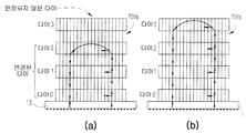
도 7의 (a) 내지 도 8의 (b)는, 본 발명의 예시적인 실시예에 따른 스택된 멀티-다이 패키지 장치에서의 다이-레벨 연결의 재구성의 예를 개략적으로 예시한다.
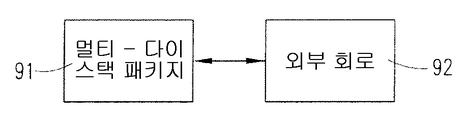
도 9는, 본 발명의 예시적인 실시예에 따른 스택된 멀티-다이 패키지 장치를 포함하는 시스템을 개략적으로 예시한다.1 is a schematic illustration of a stacked multi-die package apparatus in accordance with an exemplary embodiment of the present invention.
2 is a schematic diagram illustrating in more detail the TSV router of FIG. 1 in accordance with an exemplary embodiment of the present invention.
3 is a diagram schematically illustrating a communication link between TSV router controllers in a die of a stacked multi-die package apparatus according to an exemplary embodiment of the present invention.
4 is a diagram schematically illustrating an example of TSV reassignment supported by a stacked multi-die package apparatus according to an exemplary embodiment of the present invention.
5A and 5B are timing diagrams of signaling operations respectively associated with read and write registers in a TSV router controller of a stacked multi-die package apparatus according to an exemplary embodiment of the present invention.
6 is a schematic diagram illustrating in more detail a slave die in a stacked multi-die package apparatus according to an exemplary embodiment of the present invention.
7A-8B schematically illustrate an example of reconfiguration of a die-level connection in a stacked multi-die package apparatus according to an exemplary embodiment of the present invention.
9 schematically illustrates a system including a stacked multi-die package apparatus in accordance with an exemplary embodiment of the present invention.
본 발명의 예시적인 실시예는, 스택된 멀티-다이 패키지에서의 TSVs가, 프로그램 가능한 레지스터에 의해 제어될 수 있는 라우터를 사용하여 원하는 대로 다른 연결 구성을 갖게 한다. 여러 가지 실시예에서, 다이 사이에서 또는 다이와 기판 사이에서의 연결이 재구성된다. 레지스터에 저장된 값을 변경시킴으로써, 사용자는, 정상 미션 모드에서 패키지의 필드 동작 동안, 영향을 받은 다이를, 예컨대 공장 디폴트 연결과는 다른 방식으로 연결할 수 있다. 예컨대, 다이의 고유 회로의 I/O(입력 및/또는 출력)로의 TSV 연결이 변화할 수 있음에 따라, 다이가 스택으로부터 완전히 단절될 수 있거나, 공장 디폴트 구성에서 스택으로부터 원래 단절되었던 다이가 연결될 수 있다.Exemplary embodiments of the invention allow TSVs in a stacked multi-die package to have different connection configurations as desired using routers that can be controlled by programmable registers. In various embodiments, the connection between the dies or between the die and the substrate is reconfigured. By changing the value stored in the register, the user can connect the affected die during the field operation of the package in normal mission mode, for example in a different way than the factory default connection. For example, as the TSV connection to the I / O (input and / or output) of the die's native circuit may change, the die may be disconnected completely from the stack, or the die that originally disconnected from the stack in the factory default configuration may be connected. Can be.
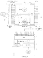
도 1은, 본 발명의 예시적인 실시예에 따른 스택된 집적회로 다이를 포함하는 멀티-칩 패키지를 개략적으로 예시한다. 마스터 다이(11)는 패키지의 외부 단자(예컨대, 패키지 리드)에 연결된다. 하나 이상의 슬레이브 다이가 마스터 다이(11) 위에 스택될 수 있다. (물리적인 스택을 도 1의 개략적인 도면에서 명시적으로 도시하고 있지 않을지라도, 이것은 당업자에게 이해될 것이다.) 도 1은, 마스터 다이(11)에 물리적으로 정반대편에서 스택에 위치할 슬레이브 다이(12)를 명시적으로 도시한다. 중간의 스택된 슬레이브 다이(12)를 집합적으로 12A로 표시한다. 점선(100)은 마스터 다이(11)의 TSVs와 마스터 다이(11) 인접한 슬레이브 다이의 축방향으로 정렬된 TSVs 각각 사이의 연결을 나타낸다. 점선(101)은 슬레이브 다이(12)의 TSVs와 슬레이브 다이(12) 인접 슬레이브 다이의 축방향으로 정렬된 TSVs 각각 사이의 연결을 나타낸다. 12A로 표시된, 중간의 스택된 슬레이브 다이의 인접한 다이 사이의 TSV 연결은 명시적으로 도시하지 않는다. 집적회로 다이의 스택을 서로 전기적으로 연결된 인접한 다이의 각 쌍의 축방향으로 할당된 각각의 TSVs로 패키징하는 것이 종래기술에서 알려져 있다. 1 schematically illustrates a multi-chip package including a stacked integrated circuit die in accordance with an exemplary embodiment of the present invention. The master die 11 is connected to an external terminal of the package (eg, package lead). One or more slave dies may be stacked above the master die 11. (Although the physical stack is not explicitly shown in the schematic diagram of FIG. 1, this will be understood by those skilled in the art.) FIG. 1 shows a slave die that will be located in the stack physically opposite to the master die 11. (12) is shown explicitly. The intermediate stacked slave dies 12 are collectively labeled 12A. The dashed
전형적으로, 다수의 TSVs가 각각의 다이 상에 제조되어 다이를 관통해 연장하여 다이의 각각의 정반대편 상의 인접한 다이의 TSVs에 연결된다. TSVs의 서브세트가, 스택에서의 다이 사이에서 신호 및/또는 전력을 연결하기 위해 설계에 의해 선택된다. 본 발명의 예시적인 실시예는, 칩 설계에 사용하기 위해 할당되지도 고장난 TSVs를 교체하는데 사용되지도 않았던 남은(스페어) TSVs를 이용한다. 이들 스페어 TSVs는 미래에 서로 다른 연결 구성을 구축하는데 이용 가능하게 된다.Typically, multiple TSVs are fabricated on each die and extend through the die to connect to TSVs of adjacent die on each opposite side of the die. A subset of TSVs is selected by the design to connect signals and / or power between dies in the stack. Exemplary embodiments of the present invention utilize the remaining (spare) TSVs that have not been allocated for use in chip design or used to replace failed TSVs. These spare TSVs will be available to build different connection configurations in the future.
도 1의 마스터 다이(11)는 패키지 기판(13)(일부 실시예에서는 인쇄회로 기판)을 통해 패키징된 멀티-다이 스택의 외부 단자에 연결된다. 마스터 다이(11)는 TSVs(18), TSV 라우터(14), TSV 라우터 제어기(15), 및 마스터 다이(11)의 정상 기능을 구현하는 고유 회로를 포함한다. 슬레이브 다이(12)는 TSVs(19), TSV 라우터(14), TSV 라우터 제어기(17), 및 그 자신의 고유 회로를 포함한다.The master die 11 of FIG. 1 is connected to an external terminal of a packaged multi-die stack via a package substrate 13 (printed circuit board in some embodiments). The master die 11 includes
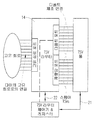
도 2는, 본 발명의 예시적인 실시예에 따른 TSV 라우터(14)를 더 상세하게 개략적으로 예시한다. 라우터(14)는, 스택된 멀티-다이 패키지의 의도한 동작에 필요한 신호 및 전력을 전달하기 위해 칩 설계에 의해 할당된 다이의 그러한 TSVs에 연결된 디폴트 포트를 포함한다. 이들 TSVs는 본 명세서에서 또한 디폴트 TSVs라고 한다. 이 설계는 또한 디폴트 TSVs를 할당하여, 다이를 통해 신호 및/또는 전력을 전송할 수 있어, 다이의 정반대편 상의 인접한 다이에 의해 사용할 수 도 있다. 라우터(14)는 다이의 고유 회로와 인터페이스하기 위한 고유 회로 포트를 더 포함한다. 원래 제조된 바와 같은 다이의 초기 디폴트 구성에서, 라우터(14)는 디폴트 포트와 고유 회로 포트 사이에 적절한 연결을 구현하여 디폴트 TSVs를 원하는 대로 고유 회로에 연결한다. 2 schematically illustrates
본 개시를 위해, 라우터가 스위치, 멀티플렉서, 또는 다수의 입력 중 임의의 하나를 출력 포트에 선택적으로 연결하는 종래기술에 알려진 임의의 다른 수단을 포함함을 주목해야 한다.It should be noted that for the present disclosure, a router includes a switch, a multiplexer, or any other means known in the art to selectively connect any one of a number of inputs to an output port.
지금까지, 남은 스페어 TSVs는 초기 제조 공정 동안을 제외하고는 사용되지 않았고, 이때 이들은 이 제조 공정 동안에 식별된 고장난 TSVs를 교체하기 위한 여분용으로 이용 가능하다. 본 발명에 따르면, 라우터(14)는 스페어 TSVs에 연결된 재할당 포트를 포함한다. 이들 스페어 TSVs는 따라서, 그 정상 미션 모드에서 패키지의 필드 동작 동안 스택된 멀티-다이 패키지 내에서, 연결 재구성 시 및/또는 새로운 연결 구성 시 사용하는데 이용 가능하다.To date, the remaining spare TSVs have not been used except during the initial manufacturing process, at which time they are available as a spare to replace the failed TSVs identified during this manufacturing process. According to the present invention, the
도 2는 또한, 여러 실시예에서, 라우터 제어기(도 1의 15 및 17을 또한 참조)는 라우터(14)를 통해(점선 참조) 또는 전용 연결(21)에 의해 관련 다이의 디폴트 TSVs에 연결될 수 있다. 제어기의 프로그램 가능한 레지스터는 TSVs를 통해 액세스될 수 있고 제어 연결(22)을 통해 라우터(14)를 제어하는데 사용될 수 있어, 스페어 TSVs를 할당하여 이미 다른 방식으로 연결된 신호를 재연결 또는 단절하거나, 이전에 존재하지 않았던 새로운 연결을 이룰 수 도 있다.FIG. 2 also shows, in various embodiments, that the router controller (see also 15 and 17 of FIG. 1) may be connected to the default TSVs of the associated die via router 14 (see dashed line) or by
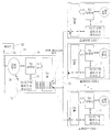
도 3은, 라우터 제어기가 상호연결된 다이의 TSVs를 포함하는 전용 링크를 통해 상호연결되는 여러 개의 슬레이브 다이(12)(슬레이브 다이(1-n)로도 표시됨)와 마스터 다이(11)를 도시한다. 일부 실시예에서, 전용 링크는 마스터 제어기(15)로부터 각각의 슬레이브 제어기(17)로의 각각의 별도의 연결의 형태일 수 도 있다. 이것은 도 3에서 점선 연결로 표시된다. 일부 실시예에서, 하나의 병렬 링크가 마스터 제어기를 공유된 버스(31) 상의 모든 슬레이브 제어기에 연결한다. 별도의 제어기 상호연결을 갖는 점선 실시예에서, 마스터 제어기(15)는 각 슬레이브 제어기(17)에 대해 하나씩 다수의 별도의 포트를 갖는다. 따라서 이들 실시예는 그러한 수의 슬레이브 다이만을 수용한다. 다른 한편, 공유된 버스 실시예는 슬레이브 다이를 식별하기 위한 어드레스만큼의 슬레이브 다이를 수용한다. 따라서 지원될 수 있는 슬레이브 다이의 수는 공유된 버스(31)에 의해 지원되는 장치 어드레스 필드의 폭에만 의존한다.3 shows a number of slave dies 12 (also represented as slave dies 1-n) and master dies 11, in which the router controllers are interconnected via dedicated links containing TSVs of interconnected dies. In some embodiments, the dedicated link may be in the form of each separate connection from the
일부 실시예는, 기존의 연결을 끊는 것 및/또는 새로운 연결을 하는 것에 대응하는 특정한 값으로 관련 라우터 제어기의 하나 이상의 레지스터를 프로그래밍함으로써, 다이의 TSVs를 재할당한다. 일반적으로, 사용자는, 스택에서 다이(예컨대 마스터)의 라우터 제어기의 레지스터로의 연결 값을 프로그래밍하며, 이것은 이제 스택 내의 다른 다이의 대응하는 레지스터에 영향을 미친다. 이러한 식으로, 스택의 모든 다이 사이의 TSV 연결 구성은 조정될 수 있다.Some embodiments reallocate TSVs of the die by programming one or more registers of the associated router controller to specific values corresponding to breaking existing connections and / or making new connections. In general, a user programs a connection value from a stack to a register of a router controller of a die (such as a master), which now affects the corresponding register of another die in the stack. In this way, the TSV connection configuration between all dies in the stack can be adjusted.
도 3을 다시 참조하면, 일부 실시예에서, 사용자는 표시된 명령을 사용하여 마스터 다이(11) 상의 적절한 라우터 제어기 레지스터(들)를 재프로그래밍하며, 다이(11)는 외부 패키지 리드(103)에 연결되어 외부 제어기(102)로부터 사용자 명령을 수신한다(도 1을 또한 참조). 일부 실시예에서, 연결(103)은 마스터 다이(11)의 TSVs, 패키지 기판 및 외부 패키지 단자를 통해 이뤄진다. 마스터 다이 상에서, 고유 회로는 라우터 제어기(15)로의 포트(38)를 가지며, 거기에 있는 레지스터에 대한 판독/기록 액세스에 사용된다. 일부 실시예에서, TSV 제어기(15)는 TSV 라우터 제어기 링크(예컨대, 공유된 버스(31))를 사용하여 그 새롭게 기록된 레지스터 값(또는 원하는 TSV 구성에 필요한 대응하는 값)을 TSV 연결의 원하는 재구성에 수반되는 임의의 슬레이브 다이(또는 다이)의 라우터 제어기 레지스터에 복사한다. 마스터 다이(11)의 라우터 제어기(15)는, 명령에 포함된 정보로부터, 그 레지스터 및 영향받은 슬레이브 다이 제어기(17)의 레지스터에 기록되어야 하는 적절한 값을 결정하여, 스택에 대한 원하는 TSV 구성을 실현한다.Referring back to FIG. 3, in some embodiments, the user reprograms the appropriate router controller register (s) on the master die 11 using the indicated instructions, and the
도 4는 본 발명의 예시적인 실시예에 따른 기존의 연결의 재구성을 도시한다. 도 4의 상부는, 제조 시 서비스 중인 전체 이용 가능한 TSVs의 서브세트(도 4에서 서비스 중인 짙은(darkened) TSV 라인으로 도시됨)를 갖는 다이 스택을 도시한다. 미션 모드에서 사용하는 동안의 일부 시간에, 다이 스택의 스페어 TSV 연결은, 도 4의 하부에서 원래의 서비스 중인 TSVs(다른 서비스 중인 짙은 TSV 라인으로 도시됨)가 아닌 TSVs를 사용하도록 재구성될 수 있다. 일반적으로, 명령은 라우터 제어기 중 하나 이상의 레지스터를 프로그래밍하도록 발행되며, 그리하여 관련 TSV 라우터(들)가 관련 연결을 재할당하게 한다. 이러한 동작은 도 5에 도시된 바와 같은 고유한 명령을 갖는 일부 실시예에서 행해진다. 명령은 필요한 장치 어드레스(DA)와 명령 정보(CMD)를 갖는다. 일부 실시예에서, 레지스터는 도 5의 (a)에 대해 후술될 바와 같이 판독될 수 있거나, 도 5의 (b)에 대해 후술될 바와 같이 기록될 수 있다. 레지스터 기록(프로그래밍) 동작의 경우, 일부 실시예는 레지스터 어드레스 및 그 대응하는 기록 데이터를 쌍으로 공급한다. 데이터뿐만 아니라 타겟 레지스터 어드레스를 공급함으로써, 제어기는 다른 기록 가능한 레지스터 타입에 필요한 바와 같이 레지스터 그룹의 모든 필드에 대한 정확한 데이터를 발행하지 않아도 된다. 따라서, 제어기는 모든 기존의 레지스터 값의 맵을 보관하거나, 후속한 재프로그래밍을 위해 먼저는 레지스터 값을 판독하는 것과 같은 부담을 피한다.4 illustrates a reconfiguration of an existing connection according to an exemplary embodiment of the present invention. The top of FIG. 4 shows a die stack with a subset of the total available TSVs in service during manufacture (shown as the darkened TSV lines in service in FIG. 4). At some time during use in mission mode, the spare TSV connections of the die stack may be reconfigured to use TSVs other than the original serving TSVs (shown in other serving thick TSV lines) at the bottom of FIG. . In general, instructions are issued to program one or more registers of the router controller, thereby causing the associated TSV router (s) to reallocate the associated connections. This operation is done in some embodiments with unique instructions as shown in FIG. The command has the necessary device address DA and command information CMD. In some embodiments, the register may be read as described below with respect to FIG. 5A, or may be written as described below with reference to FIG. 5B. In the case of a register write (programming) operation, some embodiments supply a register address and its corresponding write data in pairs. By supplying the target register address as well as the data, the controller does not have to issue the correct data for all fields of the register group as required for other writable register types. Thus, the controller avoids the burden of keeping a map of all existing register values, or first reading the register values for subsequent reprogramming.
도 5의 (a)는 본 발명의 예시적인 실시예에 따른 TSV 할당 레지스터를 판독하는데 사용되는 명령을 도시한다. 일부 실시예에서, 명령 패킷은 종래의 프로토콜을 따른다. 특히, CSI(Command Strobe Input)가 하이일 때, 장치 어드레스, 그 다음에 명령 바이트 및 레지스터 어드레스 바이트(들)가 버스(예컨대, 도 3의 공유된 버스(31)) 상으로 구동되어, 명령 패킷에서 주어진 어드레스에서의 레지스터로부터 시작하여 TSV 할당 레지스터를 판독하도록 타겟 장치를 프라이밍한다(priming).5A illustrates an instruction used to read a TSV assignment register in accordance with an exemplary embodiment of the present invention. In some embodiments, the command packet follows a conventional protocol. In particular, when the Command Strobe Input (CSI) is high, the device address, followed by the command byte and register address byte (s), is driven onto the bus (e.g., shared
미리 결정된 시간(흔히 전형적인 장치 데이터 시트에서 tCDS라고 함)이 경과한 후, 제어기는, 명령 패킷에 명시된 어드레스에서 시작하여, 현재의 레지스터 데이터로 버스를 구동하도록 타겟 장치에 시그널링하는 DSI(Data Strobe Input)를 어서팅한다(assert). 타겟 장치는 내부적으로 그 어드레스 포인터를 증분시키며, DSI가 하이인 한 또는 레지스터 어드레스 공간의 끝에 도달할 때까지 연속적인 레지스터 어드레스로부터 데이터를 드라이브 아웃(drive out)한다. 이것이, DSI 어서션 이후의 버스 활동으로 나타내어진 명령에 대한 다이의 응답을 구성한다.After a predetermined amount of time (often referred to as t CDS in a typical device data sheet), the controller starts at the address specified in the command packet and signals the target device to drive the bus with the current register data. Assert Input. The target device internally increments its address pointer and drives out data from consecutive register addresses as long as the DSI is high or until the end of the register address space is reached. This constitutes the die's response to the command represented by the bus activity after the DSI assertion.
도 5의 (b)는, 본 발명의 예시적인 실시예에 따른 멀티-칩 패키지에서 TSVs의 할당을 변화시키는데 사용되는 명령 패킷을 도시한다. 일부 실시예에서, 명령 패킷은 일반적으로 도 5의 (a)에 의해 예시된 종래의 프로토콜을 따르며, 장치 어드레스, 그 다음에 명령 바이트, 그 다음에 어드레스/데이터 바이트-쌍을 포함한다. 레지스터 어드레스 및 대응하는 데이터가 쌍으로 제공되며, 각각 여러 실시예에서 한 바이트 이상의 길이를 가질 수 있다. 이들 상세한 내용은 장치 설계 파라미터에 의존하며, 장치 데이터 시트에 명시될 것이다. 예컨대, 더 많은 TSVs를 갖는 장치는 더 소수의 TSVs를 활용하는 장치보다 더 긴 바이트 수를 갖는 어드레스 및 데이터 필드를 필요로 할 수 있다. 각 어드레스 필드는, TSVs에 대한 신호 할당에 대한 정보를 포함하는 할당 레지스터 집합에서 고유한 레지스터를 지칭한다. 명령 패킷 데이터 필드에서 제공된 데이터는 명시된 할당 레지스터에 데이터를 중복 기록하여(over-writes), 새로운 TSV/신호 할당을 구현한다.5B illustrates a command packet used to change the allocation of TSVs in a multi-chip package according to an exemplary embodiment of the present invention. In some embodiments, the command packet generally follows the conventional protocol illustrated by FIG. 5A and includes a device address, then a command byte, and then an address / data byte-pair. Register addresses and corresponding data are provided in pairs, each of which may have a length of one or more bytes in various embodiments. These details depend on the device design parameters and will be specified in the device data sheet. For example, a device with more TSVs may require an address and data field with a longer number of bytes than a device utilizing fewer TSVs. Each address field refers to a register that is unique in a set of allocation registers that contains information about signal allocation for TSVs. The data provided in the command packet data field over-writes the data in the specified assignment register to implement a new TSV / signal assignment.
이전에 연결되지 않았던 고유 다이 회로를 연결하기 위한 예시적인 실시예를 도 6에서 개략적으로 예시한다. TSVs는, 디폴트 제조 구성에서 연결되지 않았던 스택 패키지 서브-회로(일반적으로 Cct1-Cctn으로 표시됨)에 연결하거나, 디폴트 제조 구성에서 연결되었던 스택 패키지 선택된 서브-회로로부터 단절하는데 사용될 수 있다.An exemplary embodiment for connecting a unique die circuit that was not previously connected is schematically illustrated in FIG. 6. TSVs can be used to connect to stack package sub-circuits (typically denoted Cct1-Cctn) that were not connected in the default fabrication configuration, or disconnect from the stack package selected sub-circuits that were connected in the default fabrication configuration.
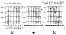
도 7은, 본 발명의 예시적인 실시예에 따라 스택으로부터 다이를 추가/제거하거나 링 아키텍처로부터 다이를 추가/제거하는 것을 개략적으로 예시한다. 예컨대, 스택된 메모리 패키지는 그 다이 중 하나가 메모리 인터페이스나 링 아키텍처로부터 제거될 수 있거나, 미래에 인터페이스/링에 추가될 수 있는 "스페어" 다이를 포함할 수 있다. 도 7에서 다이 0은 마스터 다이(11)일 수 있고, 이때 나머지 다이(다이 1 내지 다이 3)는 슬레이브 다이(12)이다. 도 7은, 상부 다이(도 7의 (b))나 중간 다이(도 7의 (c))가 도 7의 (a)의 인터페이스/링 구성으로부터 제거되는 상황을 도시한다. 일부 실시예에서, 사용자는 외부 제어기(102)(도 1 및 도 3을 또한 참조)를 동작하여, 영향받은 다이의 TSV 라우터가, 현재의 구성에서 고유 회로에 연결된 다이의 TSVs 중 선택된 다이를 다이의 고유 회로로부터 단절함으로써, 다이의 현재의 TSV 구성을 변경하게 하는 적절한 명령을 발행한다. 일부 실시예에서, 외부 제어기(102)는 OS(운영체계) 또는 패키지에서 미리 결정된 조건을 검출하는 제어기 마이크로코드에 자동으로 응답하여 명령을 발행한다.7 schematically illustrates adding / removing a die from a stack or adding / removing a die from a ring architecture in accordance with an exemplary embodiment of the present invention. For example, a stacked memory package may include a "spare" die, one of which die may be removed from the memory interface or ring architecture, or may be added to the interface / ring in the future. In FIG. 7, die 0 may be a master die 11, with the remaining dies (die 1 to die 3) being slave dies 12. FIG. 7 illustrates a situation in which the upper die (FIG. 7B) or the intermediate die (FIG. 7C) is removed from the interface / ring configuration of FIG. 7A. In some embodiments, a user operates an external controller 102 (see also FIGS. 1 and 3) such that the TSV router of the affected die dies selected dies of TSVs of the die connected to the unique circuit in the current configuration. By disconnecting from the inherent circuit, the appropriate command is issued to change the current TSV configuration of the die. In some embodiments,
도 8의 (a)는, 사용자에 의해 또는 자동 소프트웨어/하드웨어 제어에 의해 선택적으로 연결될 수 있는 "스페어" 다이(다이 3)를 포함하는 본 발명의 예시적인 실시예에 따른 장치 스택을 도시한다. 하나 이상의 스페어 플래시 다이를 포함하는 멀티-칩 패키지 플래시 메모리 장치에서 예시적으로 응용된다. 더 많은 메모리 용량이 필요하다면, 도 8의 (b)에 도시된 바와 같이 스페어 다이가 인터페이스/링에 추가될 수 있다. 다른 예로서, 도 8의 (a)에서 하나의 다이가 고장 난 경우, 이것은 제거되어 스페어 다이로 교체될 수 있어, 궁극적으로는 도 7의 (c)에 도시한 구성에 이르게 되어, 멀티-칩 패키지의 유효 수명을 연장한다. 여러 가지 실시예에서, 다이 교체 공정은 특정 다이 상의 어떤 역치에 도달한 에러에 의해서, 다이 상의 고유 회로의 미리 결정된 수의 서브-회로의 고장에 의해, 또는 특정 서브-회로의 고장에 의해 트리거될 수 있다. 이 조건이 검출될 경우, 적절한 명령(또는 명령들)이 스페어 다이 및 고장난 다이의 TSV 라우터 제어기가 예컨대: (1) 스페어 다이를 인터페이스/링에 연결; (2) 데이터를 고장난 다이로부터 스페어 다이로 전송; 및 (3) 고장난 다이를 인터페이스/링으로부터 단절과 같은 적절한 치료 절차의 실행에 참여하게 한다.8A shows a device stack according to an exemplary embodiment of the present invention that includes a “spare” die (die 3) that can be selectively connected by a user or by automatic software / hardware control. Example applications are in multi-chip package flash memory devices that include one or more spare flash dies. If more memory capacity is needed, a spare die may be added to the interface / ring as shown in FIG. 8 (b). As another example, if one die in Fig. 8A fails, it can be removed and replaced with a spare die, ultimately leading to the configuration shown in Fig. 7C, resulting in a multi-chip Extend the useful life of the package. In various embodiments, the die replacement process may be triggered by an error in reaching a certain threshold on a particular die, by a failure of a predetermined number of sub-circuits of a specific circuit on a die, or by a failure of a particular sub-circuit. Can be. If this condition is detected, an appropriate command (or instructions) is passed to the spare die and the failed die TSV router controller, for example: (1) connecting the spare die to the interface / ring; (2) transfer data from the failed die to the spare die; And (3) engage the failed die in the execution of appropriate treatment procedures such as disconnection from the interface / ring.
도 9는 본 발명의 예시적인 실시예에 따른 실시예를 개략적으로 예시한다. 멀티-다이 스택 패키지(91), 예컨대 도 1 내지 도 8의 (b)에 대해 상술한 바와 같은 패키지가 외부 전자 회로(92)와 통신하기 위해 결합된다. 일부 실시예에서, 패키지(91)는 데이터 저장 기능, 예컨대 플래시 메모리 기능을 구현한다. 일부 실시예에서, 패키지(91)는 임의의 원하는 주문형 기능, 예컨대 디지털 데이터 처리를 구현한다. 여러 가지 실시예에서, 전자 회로(92)는, 패키지(91)에 의해 구현된 기능을 활용 및/또는 제어하는 회로의 임의의 집합, 예컨대 패키지(91)에 의해 구현된 데이터 저장 기능과 협력할 수 있는 메모리 제어기일 수 있고, 도 1 내지 도 8에 관해 상술한 바와 같이 제어기(102)의 기능을 구현할 수 있다.9 schematically illustrates an embodiment according to an exemplary embodiment of the present invention. The
예시적인 실시예를 상세하게 상술하였을 지라도, 이것은, 여러 가지 실시예에서 실행될 수 있는 본 발명의 범위를 제한하지 않는다.Although the exemplary embodiments have been described in detail above, this does not limit the scope of the invention which may be practiced in various embodiments.
Claims (26)
상기 다이를 관통해 연장하여, 상기 다이 상에서 신호에 대한 외부 액세스를 제공하는 제 1 다수의 비아; 및
상기 비아에 결합된 라우터로서, 상기 제 1 다수의 비아로 하여금 다수의 신호-전달 구성 중 선택된 구성을 갖게 하도록 구성되는 라우터를 포함하고;
상기 선택된 신호-전달 구성에서, 적어도 하나의 비아는, 상기 적어도 하나의 비아가 상기 신호-전달 구성 중 다른 구성에서 전달하지 않는 적어도 하나의 신호를 전달하는, 집적회로 다이.As an integrated circuit die,
A first plurality of vias extending through the die to provide external access to signals on the die; And
A router coupled to the via, the router comprising a router configured to cause the first plurality of vias to have a selected one of a plurality of signal-delivery configurations;
In the selected signal-carrying configuration, at least one via carries at least one signal that the at least one via does not carry in another of the signal-carrying configurations.
다이를 관통해 연장하여 상기 다이 상에서 신호에 대한 외부 액세스를 제공하는 다수의 비아로 하여금 라우터를 사용하여 제 1 신호-전달 구성을 갖게 하는 단계; 및
상기 다수의 비아가 상기 라우터를 사용하여 제 2 신호-전달 구성을 갖게 하는 단계를 포함하며;
상기 제 1 신호-전달 구성에서, 상기 비아 중 적어도 하나의 비아는, 상기 적어도 하나의 비아가 상기 제 2 신호-전달 구성에서 전달하지 않는 관련된 적어도 하나의 신호를 전달하는, 집적회로 다이 동작 방법.An integrated circuit die operating method,
Allowing a plurality of vias extending through the die to provide external access to signals on the die to have a first signal-transfer configuration using a router; And
Causing the plurality of vias to have a second signal-delivery configuration using the router;
In the first signal-carrying configuration, at least one of the vias conveys at least one associated signal that the at least one via does not carry in the second signal-carrying configuration.
다수의 집적회로 다이를 포함하되, 각 다이는:
다이를 관통해 연장하여 다이 상에서 신호에 대한 외부 액세스를 제공하는 다수의 비아로서, 상기 다수의 다이는, 각 다이의 비아가 인접한 다이의 비아에 연결되도록 스택으로 배치되는, 다수의 비아; 및
관련된 비아에 결합되는 라우터로서:
상기 관련된 비아로 하여금, 상기 다이의 고유 회로가, 인접한 다이와 시그널링하기 위해 상기 관련된 비아 중 선택된 비아에 의해 연결되는 시그널링 연결 구성을 갖게 하고; 및
상기 관련된 비아로 하여금, 상기 다이의 고유 회로가 상기 인접한 다이와 시그널링하기 위해 연결되지 않는 시그널링 단절 구성을 갖게 하도록 구성되는 라우터를 포함하는, 스택된 집적회로 장치.A stacked integrated circuit device,
Including multiple integrated circuit dies, each die:
A plurality of vias extending through the die to provide external access to signals on the die, the plurality of dies comprising: a plurality of vias arranged in a stack such that vias of each die are connected to vias of adjacent dies; And
As a router coupled to the relevant vias:
Cause the associated via to have a unique circuitry of the die having a signaling connection configuration that is connected by a selected one of the associated vias for signaling with an adjacent die; And
And a router configured to cause the associated via to have a signaling disconnection configuration in which the unique circuitry of the die is not connected to signal with the adjacent die.
청구항 1에 기재된 다수의 집적회로 다이를 포함하고;
상기 다수의 다이가, 각 다이의 비아가 인접한 다이의 비아에 연결되도록 스택으로 배치되는, 스택된 집적회로 장치.A stacked integrated circuit device,
A plurality of integrated circuit dies as claimed in claim 1;
And the plurality of dies are arranged in a stack such that vias of each die are connected to vias of adjacent dies.
적어도 하나의 다이의 비아로 하여금, 상기 적어도 하나의 다이의 고유 회로가 인접한 다이와 시그널링하기 위해 상기 비아 중 선택된 비아에 의해 연결되는 시그널링 연결 구성을 갖게 하는 단계; 및
상기 적어도 하나의 다이의 비아로 하여금, 상기 적어도 하나의 다이의 고유 회로가 상기 인접한 다이와 시그널링하기 위해 연결되지 않는 시그널링 단절 구성을 갖게 하는 단계를 포함하는, 방법.A method of operating a plurality of stacked integrated circuit dies, each die including a plurality of vias extending through to provide external access to signals on the die, the vias of each die being connected to vias of adjacent dies,
Causing a via of at least one die to have a signaling connection configuration wherein a unique circuit of the at least one die is connected by a selected one of the vias for signaling with an adjacent die; And
Causing the vias of the at least one die to have a signaling disconnection configuration in which the unique circuitry of the at least one die is not coupled to signal with the adjacent die.
상기 스택된 집적회로 장치 외부에 제공되고 상기 장치에 결합되어 상기 장치와 통신하는 전자 회로를 포함하는, 시스템.A stacked integrated circuit device according to claim 17; And
And electronic circuitry external to the stacked integrated circuit device and coupled to and in communication with the device.
상기 스택된 집적회로 장치 외부에 제공되고 상기 장치에 결합되어 상기 장치와 통신하는 전자 회로를 포함하는, 시스템.A stacked integrated circuit device according to claim 15; And
And electronic circuitry external to the stacked integrated circuit device and coupled to and in communication with the device.
Applications Claiming Priority (5)
| Application Number | Priority Date | Filing Date | Title |
|---|---|---|---|
| US25286509P | 2009-10-19 | 2009-10-19 | |
| US61/252,865 | 2009-10-19 | ||
| US12/773,340 US8604593B2 (en) | 2009-10-19 | 2010-05-04 | Reconfiguring through silicon vias in stacked multi-die packages |
| US12/773,340 | 2010-05-04 | ||
| PCT/CA2010/001650 WO2011047470A1 (en) | 2009-10-19 | 2010-10-19 | Reconfiguring through silicon vias in stacked multi-die packages |
Publications (1)
| Publication Number | Publication Date |
|---|---|
| KR20120085650A true KR20120085650A (en) | 2012-08-01 |
Family
ID=43878833
Family Applications (1)
| Application Number | Title | Priority Date | Filing Date |
|---|---|---|---|
| KR1020117011810A KR20120085650A (en) | 2009-10-19 | 2010-10-19 | Reconfiguring through silicon vias in stacked multi-die packages |
Country Status (7)
| Country | Link |
|---|---|
| US (2) | US8604593B2 (en) |
| EP (1) | EP2491589A4 (en) |
| JP (1) | JP2013508941A (en) |
| KR (1) | KR20120085650A (en) |
| CN (1) | CN102227806A (en) |
| TW (1) | TWI476889B (en) |
| WO (1) | WO2011047470A1 (en) |
Families Citing this family (30)
| Publication number | Priority date | Publication date | Assignee | Title |
|---|---|---|---|---|
| US9229887B2 (en) * | 2008-02-19 | 2016-01-05 | Micron Technology, Inc. | Memory device with network on chip methods, apparatus, and systems |
| US7978721B2 (en) | 2008-07-02 | 2011-07-12 | Micron Technology Inc. | Multi-serial interface stacked-die memory architecture |
| US8086913B2 (en) | 2008-09-11 | 2011-12-27 | Micron Technology, Inc. | Methods, apparatus, and systems to repair memory |
| US9123552B2 (en) * | 2010-03-30 | 2015-09-01 | Micron Technology, Inc. | Apparatuses enabling concurrent communication between an interface die and a plurality of dice stacks, interleaved conductive paths in stacked devices, and methods for forming and operating the same |
| US8362602B2 (en) * | 2010-08-09 | 2013-01-29 | Headway Technologies, Inc. | Layered chip package and method of manufacturing same |
| US8916910B2 (en) * | 2010-12-13 | 2014-12-23 | Research Foundation Of State University Of New York | Reconfigurable RF/digital hybrid 3D interconnect |
| KR101817156B1 (en) * | 2010-12-28 | 2018-01-10 | 삼성전자 주식회사 | Semiconductor device of stacked structure having through electrode, semiconductor memory device, semiconductor memory system and operating method thereof |
| KR101208962B1 (en) * | 2011-02-22 | 2012-12-06 | 에스케이하이닉스 주식회사 | Semiconductor apparatus |
| US8624626B2 (en) | 2011-11-14 | 2014-01-07 | Taiwan Semiconductor Manufacturing Co., Ltd. | 3D IC structure and method |
| US20130159587A1 (en) * | 2011-12-15 | 2013-06-20 | Aaron Nygren | Interconnect Redundancy for Multi-Interconnect Device |
| US8933715B2 (en) | 2012-04-08 | 2015-01-13 | Elm Technology Corporation | Configurable vertical integration |
| US9448947B2 (en) * | 2012-06-01 | 2016-09-20 | Qualcomm Incorporated | Inter-chip memory interface structure |
| US9478502B2 (en) * | 2012-07-26 | 2016-10-25 | Micron Technology, Inc. | Device identification assignment and total device number detection |
| US9026872B2 (en) * | 2012-08-16 | 2015-05-05 | Xilinx, Inc. | Flexible sized die for use in multi-die integrated circuit |
| KR102058101B1 (en) * | 2012-12-20 | 2019-12-20 | 에스케이하이닉스 주식회사 | Semiconductor integrated circuit |
| KR102190382B1 (en) | 2012-12-20 | 2020-12-11 | 삼성전자주식회사 | Semiconductor package |
| US9612988B2 (en) * | 2013-07-23 | 2017-04-04 | International Business Machines Corporation | Donor cores to improve integrated circuit yield |
| US20150155039A1 (en) * | 2013-12-02 | 2015-06-04 | Silicon Storage Technology, Inc. | Three-Dimensional Flash NOR Memory System With Configurable Pins |
| US9245825B2 (en) | 2014-01-23 | 2016-01-26 | Sandisk Technologies Inc. | I/O pin capacitance reduction using TSVS |
| US9501603B2 (en) | 2014-09-05 | 2016-11-22 | International Business Machines Corporation | Integrated circuit design changes using through-silicon vias |
| US10002653B2 (en) | 2014-10-28 | 2018-06-19 | Nxp Usa, Inc. | Die stack address bus having a programmable width |
| KR102290020B1 (en) * | 2015-06-05 | 2021-08-19 | 삼성전자주식회사 | Semiconductor memory device providing analiysis and relief of soft data fail in stacked chips |
| US9871020B1 (en) * | 2016-07-14 | 2018-01-16 | Globalfoundries Inc. | Through silicon via sharing in a 3D integrated circuit |
| US10249590B2 (en) | 2017-06-06 | 2019-04-02 | Globalfoundries Inc. | Stacked dies using one or more interposers |
| US11048597B2 (en) * | 2018-05-14 | 2021-06-29 | Micron Technology, Inc. | Memory die remapping |
| US11055167B2 (en) * | 2018-05-14 | 2021-07-06 | Micron Technology, Inc. | Channel-scope proximity disturb and defect remapping scheme for non-volatile memory |
| US10838831B2 (en) * | 2018-05-14 | 2020-11-17 | Micron Technology, Inc. | Die-scope proximity disturb and defect remapping scheme for non-volatile memory |
| CN112102862B (en) * | 2020-09-22 | 2023-03-07 | 武汉新芯集成电路制造有限公司 | Chip structure, data reading processing method and chip structure manufacturing method |
| US11226767B1 (en) * | 2020-09-30 | 2022-01-18 | Micron Technology, Inc. | Apparatus with access control mechanism and methods for operating the same |
| US11468945B2 (en) * | 2020-10-15 | 2022-10-11 | Arm Limited | 3D storage architecture with tier-specific controls |
Family Cites Families (19)
| Publication number | Priority date | Publication date | Assignee | Title |
|---|---|---|---|---|
| TW511414B (en) | 2001-04-19 | 2002-11-21 | Via Tech Inc | Data processing system and method, and control chip, and printed circuit board thereof |
| US20030040166A1 (en) | 2001-05-25 | 2003-02-27 | Mark Moshayedi | Apparatus and method for stacking integrated circuits |
| DE102004045527B4 (en) * | 2003-10-08 | 2009-12-03 | Siemens Ag | Configurable logic circuitry |
| JP4708176B2 (en) * | 2005-12-08 | 2011-06-22 | エルピーダメモリ株式会社 | Semiconductor device |
| US7352602B2 (en) * | 2005-12-30 | 2008-04-01 | Micron Technology, Inc. | Configurable inputs and outputs for memory stacking system and method |
| US20070220207A1 (en) * | 2006-03-14 | 2007-09-20 | Bryan Black | Transferring data from stacked memory |
| TWI332239B (en) * | 2006-12-14 | 2010-10-21 | United Microelectronics Corp | Semiconductor wafer and method for forming the same |
| KR100871381B1 (en) * | 2007-06-20 | 2008-12-02 | 주식회사 하이닉스반도체 | Through silicon via chip stack package |
| US7863733B2 (en) * | 2007-07-11 | 2011-01-04 | Arm Limited | Integrated circuit with multiple layers of circuits |
| US8136071B2 (en) | 2007-09-12 | 2012-03-13 | Neal Solomon | Three dimensional integrated circuits and methods of fabrication |
| US20090072373A1 (en) * | 2007-09-14 | 2009-03-19 | Reynaldo Corpuz Javier | Packaged integrated circuits and methods to form a stacked integrated circuit package |
| US7816934B2 (en) * | 2007-10-16 | 2010-10-19 | Micron Technology, Inc. | Reconfigurable connections for stacked semiconductor devices |
| KR101176187B1 (en) | 2007-11-21 | 2012-08-22 | 삼성전자주식회사 | Stacked semiconductor device and method for thereof serial path build up |
| US7791175B2 (en) * | 2007-12-20 | 2010-09-07 | Mosaid Technologies Incorporated | Method for stacking serially-connected integrated circuits and multi-chip device made from same |
| US8384417B2 (en) * | 2008-09-10 | 2013-02-26 | Qualcomm Incorporated | Systems and methods utilizing redundancy in semiconductor chip interconnects |
| US7796446B2 (en) * | 2008-09-19 | 2010-09-14 | Qimonda Ag | Memory dies for flexible use and method for configuring memory dies |
| US8134852B2 (en) * | 2008-10-14 | 2012-03-13 | Mosaid Technologies Incorporated | Bridge device architecture for connecting discrete memory devices to a system |
| US8472199B2 (en) * | 2008-11-13 | 2013-06-25 | Mosaid Technologies Incorporated | System including a plurality of encapsulated semiconductor chips |
| US8977809B2 (en) * | 2008-11-26 | 2015-03-10 | Micron Technology, Inc. | Sharing resources in multi-dice stacks |
-
2010
- 2010-05-04 US US12/773,340 patent/US8604593B2/en active Active
- 2010-08-26 TW TW099128670A patent/TWI476889B/en not_active IP Right Cessation
- 2010-10-19 JP JP2012533445A patent/JP2013508941A/en active Pending
- 2010-10-19 KR KR1020117011810A patent/KR20120085650A/en not_active Application Discontinuation
- 2010-10-19 EP EP10824345.2A patent/EP2491589A4/en not_active Withdrawn
- 2010-10-19 WO PCT/CA2010/001650 patent/WO2011047470A1/en active Application Filing
- 2010-10-19 CN CN201080003433.2A patent/CN102227806A/en active Pending
-
2013
- 2013-12-10 US US14/101,507 patent/US9117685B2/en active Active
Also Published As
| Publication number | Publication date |
|---|---|
| CN102227806A (en) | 2011-10-26 |
| TW201126682A (en) | 2011-08-01 |
| US20140097891A1 (en) | 2014-04-10 |
| US9117685B2 (en) | 2015-08-25 |
| EP2491589A4 (en) | 2015-07-22 |
| TWI476889B (en) | 2015-03-11 |
| JP2013508941A (en) | 2013-03-07 |
| US8604593B2 (en) | 2013-12-10 |
| EP2491589A1 (en) | 2012-08-29 |
| WO2011047470A1 (en) | 2011-04-28 |
| US20110090004A1 (en) | 2011-04-21 |
Similar Documents
| Publication | Publication Date | Title |
|---|---|---|
| KR20120085650A (en) | Reconfiguring through silicon vias in stacked multi-die packages | |
| TWI756488B (en) | SYSTEM AND METHOD FOR SUPPORTING MULTI-MODE AND/OR MULTI-SPEED NON-VOLATILE MEMORY (NVM) EXPRESS (NVMe) OVER FABRICS (NVMe-oF) DEVICES AND STORAGE DEVICE | |
| US10505548B1 (en) | Multi-chip structure having configurable network-on-chip | |
| US8737105B2 (en) | Bridge device architecture for connecting discrete memory devices to a system | |
| US8917110B2 (en) | Semiconductor package including multiple chips and memory system having the same | |
| US10346325B2 (en) | Ring bus architecture for use in a memory module | |
| US8630287B2 (en) | Multiple core network device with core redundancy | |
| KR20180035175A (en) | Semiconductor device | |
| KR20070061196A (en) | Memory with flexible serial interfaces and method for accessing to memory threreof | |
| CN107704285A (en) | Field programmable gate array multi version configuration chip, system and method | |
| US11637903B2 (en) | Memory device with a multi-mode communication mechanism | |
| US20150039813A1 (en) | NAND Interface Capacity Extender Device For Extending Solid State Drives Capacity, Performance, And Reliability | |
| US7920433B2 (en) | Method and apparatus for storage device with a logic unit and method for manufacturing same | |
| US20150160890A1 (en) | Memory multi-chip package (mcp) with integral bus splitter | |
| US10565143B2 (en) | Circuitry to alleviate printed circuit board routing congestion | |
| KR100910944B1 (en) | Flash memory control apparatus and method sharing control signal |
Legal Events
| Date | Code | Title | Description |
|---|---|---|---|
| WITN | Application deemed withdrawn, e.g. because no request for examination was filed or no examination fee was paid |