JP2013508941A - Reconfiguration of through-silicon vias in stacked multi-die packages - Google Patents
Reconfiguration of through-silicon vias in stacked multi-die packages Download PDFInfo
- Publication number
- JP2013508941A JP2013508941A JP2012533445A JP2012533445A JP2013508941A JP 2013508941 A JP2013508941 A JP 2013508941A JP 2012533445 A JP2012533445 A JP 2012533445A JP 2012533445 A JP2012533445 A JP 2012533445A JP 2013508941 A JP2013508941 A JP 2013508941A
- Authority
- JP
- Japan
- Prior art keywords
- die
- vias
- integrated circuit
- configuration
- dies
- Prior art date
- Legal status (The legal status is an assumption and is not a legal conclusion. Google has not performed a legal analysis and makes no representation as to the accuracy of the status listed.)
- Pending
Links
Images


Classifications
-
- H—ELECTRICITY
- H01—ELECTRIC ELEMENTS
- H01L—SEMICONDUCTOR DEVICES NOT COVERED BY CLASS H10
- H01L23/00—Details of semiconductor or other solid state devices
- H01L23/48—Arrangements for conducting electric current to or from the solid state body in operation, e.g. leads, terminal arrangements ; Selection of materials therefor
- H01L23/50—Arrangements for conducting electric current to or from the solid state body in operation, e.g. leads, terminal arrangements ; Selection of materials therefor for integrated circuit devices, e.g. power bus, number of leads
-
- H—ELECTRICITY
- H01—ELECTRIC ELEMENTS
- H01L—SEMICONDUCTOR DEVICES NOT COVERED BY CLASS H10
- H01L25/00—Assemblies consisting of a plurality of individual semiconductor or other solid state devices ; Multistep manufacturing processes thereof
- H01L25/03—Assemblies consisting of a plurality of individual semiconductor or other solid state devices ; Multistep manufacturing processes thereof all the devices being of a type provided for in the same subgroup of groups H01L27/00 - H01L33/00, or in a single subclass of H10K, H10N, e.g. assemblies of rectifier diodes
- H01L25/04—Assemblies consisting of a plurality of individual semiconductor or other solid state devices ; Multistep manufacturing processes thereof all the devices being of a type provided for in the same subgroup of groups H01L27/00 - H01L33/00, or in a single subclass of H10K, H10N, e.g. assemblies of rectifier diodes the devices not having separate containers
- H01L25/065—Assemblies consisting of a plurality of individual semiconductor or other solid state devices ; Multistep manufacturing processes thereof all the devices being of a type provided for in the same subgroup of groups H01L27/00 - H01L33/00, or in a single subclass of H10K, H10N, e.g. assemblies of rectifier diodes the devices not having separate containers the devices being of a type provided for in group H01L27/00
- H01L25/0657—Stacked arrangements of devices
-
- G—PHYSICS
- G11—INFORMATION STORAGE
- G11C—STATIC STORES
- G11C29/00—Checking stores for correct operation ; Subsequent repair; Testing stores during standby or offline operation
- G11C29/70—Masking faults in memories by using spares or by reconfiguring
- G11C29/78—Masking faults in memories by using spares or by reconfiguring using programmable devices
- G11C29/80—Masking faults in memories by using spares or by reconfiguring using programmable devices with improved layout
- G11C29/808—Masking faults in memories by using spares or by reconfiguring using programmable devices with improved layout using a flexible replacement scheme
-
- H—ELECTRICITY
- H01—ELECTRIC ELEMENTS
- H01L—SEMICONDUCTOR DEVICES NOT COVERED BY CLASS H10
- H01L23/00—Details of semiconductor or other solid state devices
- H01L23/48—Arrangements for conducting electric current to or from the solid state body in operation, e.g. leads, terminal arrangements ; Selection of materials therefor
- H01L23/481—Internal lead connections, e.g. via connections, feedthrough structures
-
- H—ELECTRICITY
- H01—ELECTRIC ELEMENTS
- H01L—SEMICONDUCTOR DEVICES NOT COVERED BY CLASS H10
- H01L25/00—Assemblies consisting of a plurality of individual semiconductor or other solid state devices ; Multistep manufacturing processes thereof
- H01L25/18—Assemblies consisting of a plurality of individual semiconductor or other solid state devices ; Multistep manufacturing processes thereof the devices being of types provided for in two or more different subgroups of the same main group of groups H01L27/00 - H01L33/00, or in a single subclass of H10K, H10N
-
- H—ELECTRICITY
- H01—ELECTRIC ELEMENTS
- H01L—SEMICONDUCTOR DEVICES NOT COVERED BY CLASS H10
- H01L2225/00—Details relating to assemblies covered by the group H01L25/00 but not provided for in its subgroups
- H01L2225/03—All the devices being of a type provided for in the same subgroup of groups H01L27/00 - H01L33/648 and H10K99/00
- H01L2225/04—All the devices being of a type provided for in the same subgroup of groups H01L27/00 - H01L33/648 and H10K99/00 the devices not having separate containers
- H01L2225/065—All the devices being of a type provided for in the same subgroup of groups H01L27/00 - H01L33/648 and H10K99/00 the devices not having separate containers the devices being of a type provided for in group H01L27/00
- H01L2225/06503—Stacked arrangements of devices
- H01L2225/06513—Bump or bump-like direct electrical connections between devices, e.g. flip-chip connection, solder bumps
-
- H—ELECTRICITY
- H01—ELECTRIC ELEMENTS
- H01L—SEMICONDUCTOR DEVICES NOT COVERED BY CLASS H10
- H01L2225/00—Details relating to assemblies covered by the group H01L25/00 but not provided for in its subgroups
- H01L2225/03—All the devices being of a type provided for in the same subgroup of groups H01L27/00 - H01L33/648 and H10K99/00
- H01L2225/04—All the devices being of a type provided for in the same subgroup of groups H01L27/00 - H01L33/648 and H10K99/00 the devices not having separate containers
- H01L2225/065—All the devices being of a type provided for in the same subgroup of groups H01L27/00 - H01L33/648 and H10K99/00 the devices not having separate containers the devices being of a type provided for in group H01L27/00
- H01L2225/06503—Stacked arrangements of devices
- H01L2225/06527—Special adaptation of electrical connections, e.g. rewiring, engineering changes, pressure contacts, layout
-
- H—ELECTRICITY
- H01—ELECTRIC ELEMENTS
- H01L—SEMICONDUCTOR DEVICES NOT COVERED BY CLASS H10
- H01L2225/00—Details relating to assemblies covered by the group H01L25/00 but not provided for in its subgroups
- H01L2225/03—All the devices being of a type provided for in the same subgroup of groups H01L27/00 - H01L33/648 and H10K99/00
- H01L2225/04—All the devices being of a type provided for in the same subgroup of groups H01L27/00 - H01L33/648 and H10K99/00 the devices not having separate containers
- H01L2225/065—All the devices being of a type provided for in the same subgroup of groups H01L27/00 - H01L33/648 and H10K99/00 the devices not having separate containers the devices being of a type provided for in group H01L27/00
- H01L2225/06503—Stacked arrangements of devices
- H01L2225/06541—Conductive via connections through the device, e.g. vertical interconnects, through silicon via [TSV]
-
- H—ELECTRICITY
- H01—ELECTRIC ELEMENTS
- H01L—SEMICONDUCTOR DEVICES NOT COVERED BY CLASS H10
- H01L2924/00—Indexing scheme for arrangements or methods for connecting or disconnecting semiconductor or solid-state bodies as covered by H01L24/00
- H01L2924/0001—Technical content checked by a classifier
- H01L2924/0002—Not covered by any one of groups H01L24/00, H01L24/00 and H01L2224/00
Abstract
積層されたマルチダイ集積回路パッケージ内のシリコン貫通ビア(TSV)は、その標準的なミッションモードで、パッケージのフィールド動作中に、所望に応じて、別の接続構成をとるように制御される。TSV接続は、例えば、そのダイの工場デフォルト接続とは異なるやり方で、影響されたダイを接続するように再構成可能である。ダイの固有回路の入力および/または出力へのTSV接続は、変更可能である。ダイが、積層内のダイを相互接続するインターフェースから完全に切断されても、またはこのようなインターフェースから元々切断されていたダイが、インターフェースに接続されてもよい。 Through-silicon vias (TSVs) in stacked multi-die integrated circuit packages are controlled in their standard mission mode to take alternate connection configurations as desired during field operation of the package. The TSV connection can be reconfigured to connect the affected die, for example, in a manner different from the factory default connection for that die. The TSV connections to the inputs and / or outputs of the die's unique circuitry can be varied. A die may be completely disconnected from the interface that interconnects the dies in the stack, or a die that was originally disconnected from such an interface may be connected to the interface.
Description
本出願は、2009年10月19日に出願された米国特許仮出願第61/252,865号、および2010年5月4日に出願された米国特許出願第12/773,340号への優先権を主張するものであり、これらはともに参照によって本明細書に組み込まれている。 This application claims priority to U.S. Provisional Application No. 61 / 252,865, filed October 19, 2009, and U.S. Patent Application No. 12 / 773,340, filed May 4, 2010. Both of which are incorporated herein by reference.
本研究は、半導体集積回路デバイスに関するものであり、より詳細には、シリコン貫通ビア(TSV)によって相互接続された積層化構成での多重集積回路ダイのパッケージ化構成に関するものである。 This study relates to semiconductor integrated circuit devices and, more particularly, to the packaging configuration of multiple integrated circuit dies in a stacked configuration interconnected by through-silicon vias (TSV).
従来の技術は、TSVによって相互接続された隣接するダイによる積層されたマルチダイパッケージを提供している。いくつかのスペアTSVが、冗長目的でそれぞれのダイ上に設置可能であり、それによって、製造中に識別可能ないずれの不良TSVをも交換可能にする。初期の製造工程が完了した後は、ダイ上のスペアTSVは、使用されない。 The prior art provides a stacked multi-die package with adjacent dies interconnected by TSV. Several spare TSVs can be installed on each die for redundancy purposes, thereby allowing any defective TSVs that can be identified during manufacture to be replaced. After the initial manufacturing process is completed, the spare TSV on the die is not used.
そのため、積層されたマルチダイパッケージにおけるスペアTSVの使用を提供することが望ましい。 Therefore, it is desirable to provide the use of spare TSVs in stacked multi-die packages.
そのため、本発明の目的は、積層されたマルチダイパッケージにおけるスペアTSVの使用のための装置、方法、およびシステムを提供することである。 Therefore, an object of the present invention is to provide an apparatus, method and system for use of spare TSVs in stacked multi-die packages.
本発明の広範な態様によれば、集積回路ダイ装置であって、装置に対する信号に外部アクセスを供給するための、装置を通って延在する複数のビアと、前記ビアと結合され、前記ビアに、複数の信号搬送構成のうちの選択された1つをとらせるように構成されているルータとを備え、前記選択された信号搬送構成においては、前記ビアのうちの少なくとも1つは、前記少なくとも1つのビアが、別の前記信号搬送構成では搬送しない関連する少なくとも1つの信号を搬送する、装置が提供される。 In accordance with a broad aspect of the invention, an integrated circuit die device, a plurality of vias extending through the device for providing external access to signals to the device, coupled to the via, and the via A router configured to take a selected one of a plurality of signal transport configurations, wherein in the selected signal transport configuration, at least one of the vias is the An apparatus is provided wherein at least one via carries an associated at least one signal that is not carried in another said signal carrying configuration.
好ましくは、少なくとも別の前記ビアは、前記別の前記信号搬送構成で、関連する少なくとも1つの信号を搬送する。 Preferably, at least another said via carries at least one associated signal in said another signal carrying configuration.
有利には、この装置は、前記選択された信号搬送構成を示す制御信号をそれに対して供給するための前記ルータと結合されているコントローラを含む。 Advantageously, the apparatus includes a controller coupled to the router for supplying to it a control signal indicative of the selected signal transport configuration.
加えて、前記コントローラは、前記選択された信号搬送構成を示す情報を受け取り、前記情報に応答して前記制御信号を供給するように構成されている。 In addition, the controller is configured to receive information indicative of the selected signal carrier configuration and to provide the control signal in response to the information.
好都合には、前記コントローラは、前記ビアの1つの群と結合されて、前記情報を前記群のビアを通る装置の外部のソースから受け取る。 Conveniently, the controller is coupled to a group of the vias and receives the information from a source external to the device through the group of vias.
好ましくは、前記ルータは、前記情報を前記群のビアから前記コントローラにルーティングするように構成されている。 Preferably, the router is configured to route the information from the group of vias to the controller.
好都合には、外部ソースは、さらなる集積回路ダイ装置に対する信号に外部アクセスを供給するための、それを通って延在するさらなる複数のビアを有するさらなる装置である。 Conveniently, the external source is a further device having a plurality of additional vias extending therethrough for providing external access to signals for further integrated circuit die devices.
加えて、前記群のビアは、さらなる複数のビアのさらなる群に接続して、前記情報を受け取るようになされている。 In addition, the group of vias is adapted to connect to a further group of further vias to receive the information.
有利には、前記コントローラは、前記情報を、前記選択された信号搬送構成を選択する外部コントローラから受け取るようになされている。 Advantageously, the controller is adapted to receive the information from an external controller that selects the selected signal transport configuration.
利益のあるようには、前記コントローラは、前記制御信号を保存するためのレジスタを含む。 Advantageously, the controller includes a register for storing the control signal.
加えて、前記ビアの1つの群は、前記コントローラと結合されて、さらなる装置を通って延在し、さらなる装置に対する信号に外部アクセスを供給するさらなる複数のビアによってとることが可能な複数の信号搬送構成のうちの選択された1つを示す情報を、前記コントローラからさらなる集積回路ダイ装置のさらなるコントローラに転送する。 In addition, a group of the vias is coupled to the controller and extends through additional devices and can be taken by additional vias that provide external access to signals for the additional devices. Information indicating a selected one of the transport configurations is transferred from the controller to a further controller of a further integrated circuit die device.
好ましくは、装置は、前記ルータと結合されている固有回路を含み、前記信号搬送構成のそれぞれのものにおいては、前記ルータは、それぞれの信号を前記固有回路のそれぞれの部分から前記ビアのうちの同じものにルーティングする。 Preferably, the apparatus includes a unique circuit coupled to the router, and in each of the signal carrying configurations, the router transmits a respective signal from a respective portion of the unique circuit of the vias. Route to the same thing.
本発明の別の広範な態様によれば、ダイを通って延在し、ダイに対する信号に外部アクセスを供給する複数のビアに、第1の信号搬送構成をとらせるステップと、複数のビアに、第2の信号搬送構成をとらせるステップとを含み、第1の信号搬送構成においては、ビアのうちの少なくとも1つは、少なくとも1つのビアが、第2の信号搬送構成では搬送しない関連する少なくとも1つの信号を搬送する、集積回路ダイ動作の方法を提供する。 In accordance with another broad aspect of the invention, a plurality of vias extending through the die and providing external access to signals to the die have a first signal transport configuration; and Taking a second signal carrying configuration, wherein in the first signal carrying configuration, at least one of the vias is associated with at least one via not being carried in the second signal carrying configuration A method of integrated circuit die operation is provided that carries at least one signal.
好ましくは、第1および第2の信号搬送構成はそれぞれ、信号をダイ上の固有回路のそれぞれの部分からビアのうちの同じものにルーティングする。 Preferably, the first and second signal carrying configurations each route signals from respective portions of the unique circuitry on the die to the same of the vias.
本発明のさらなる別の広範な態様によれば、複数の集積回路ダイ装置を備える積層された集積回路装置が提供され、それぞれの前記集積回路ダイ装置は、集積回路ダイ装置に対する信号に外部アクセスを供給するための、それを通って延在する複数のビアを含み、前記複数の集積回路ダイ装置は、それぞれの前記集積回路ダイ装置のビアが、隣接する集積回路ダイ装置のビアにそれぞれ接続されるように積み重なって配置され、それぞれの前記集積回路ダイ装置は、関連するビアと結合され、関連するビアに、関連する集積回路ダイ装置の固有回路が、関連するビアのうちの選択されたものによって接続されて、隣接する前記集積回路ダイ装置とシグナリングするシグナリング接続構成をとらせるように構成されているルータを含み、それぞれの前記ルータはさらに、関連するビアに、関連する集積回路ダイ装置の固有回路が接続されずに、隣接する集積回路ダイ装置とシグナリングするシグナリング切断構成をとらせるように構成されている。 In accordance with yet another broad aspect of the present invention, a stacked integrated circuit device comprising a plurality of integrated circuit die devices is provided, each integrated circuit die device having external access to signals to the integrated circuit die device. A plurality of vias extending therethrough, the plurality of integrated circuit die devices each having a via in each integrated circuit die device connected to a via in an adjacent integrated circuit die device; Each of the integrated circuit die devices is coupled with an associated via, and the associated via has a unique circuit of the associated integrated circuit die device selected of the associated vias. Each of which includes a router configured to have a signaling connection configured to signal with the adjacent integrated circuit die device. The said router further related to the vias, without being connected to specific circuitry of the associated integrated circuit die apparatus is configured to assume a signaling disconnect configuration in which signaling and integrated circuit die apparatus adjacent.
好ましくは、装置は、1つの前記集積回路ダイ装置と結合されているパッケージ用基板を含む。 Preferably, the device includes a packaging substrate coupled to one of the integrated circuit die devices.
本発明のさらなる別の広範な態様によれば、複数の集積回路ダイ装置を含む積層された集積回路装置が提供され、それぞれの前記集積回路ダイ装置は、集積回路ダイ装置に対する信号に外部アクセスを供給するための、それを通って延在する複数のビアを含み、前記複数の集積回路ダイ装置は、それぞれの前記集積回路ダイ装置のビアが、隣接する集積回路ダイ装置のビアにそれぞれ接続されるように積み重なって配置され、それぞれの前記集積回路ダイ装置は、関連するビアと結合され、関連するビアに、複数の信号搬送構成のうちの選択された1つをとらせるように構成されているルータを含み、前記選択された信号搬送構成においては、関連するビアのうちの少なくとも1つは、前記少なくとも1つのビアが、別の前記信号搬送構成で搬送されない関連する少なくとも1つの信号を搬送する。 In accordance with yet another broad aspect of the present invention, a stacked integrated circuit device is provided that includes a plurality of integrated circuit die devices, each integrated circuit die device having external access to signals to the integrated circuit die device. A plurality of vias extending therethrough, the plurality of integrated circuit die devices each having a via in each integrated circuit die device connected to a via in an adjacent integrated circuit die device; Each of the integrated circuit die devices is coupled with an associated via and configured to cause the associated via to take a selected one of a plurality of signal carrying configurations. The selected signal transport configuration, wherein at least one of the associated vias is transported in another signal transport configuration Transporting the at least one signal associated not.
好ましくは、装置は、1つの前記集積回路ダイ装置と結合されているパッケージ用基板を含む。 Preferably, the device includes a packaging substrate coupled to one of the integrated circuit die devices.
本発明の別の広範な態様によれば、複数の積層された集積回路ダイ装置を動作させる方法を提供し、それぞれの集積回路ダイ装置は、集積回路ダイ装置に対する信号に外部アクセスを供給するための、それを通って延在する複数のビアを含み、それぞれの前記集積回路ダイ装置のビアは、隣接する集積回路ダイ装置のビアにそれぞれ接続され、方法は、1つの集積回路ダイ装置のビアに、1つの集積回路ダイ装置の固有回路が、ビアのうちの選択されたものによって接続されて、隣接する前記集積回路ダイ装置とシグナリングするシグナリング接続構成をとらせるステップと、1つの集積回路ダイ装置のビアに、1つの集積回路ダイ装置の固有回路が接続されずに、隣接する集積回路ダイ装置とシグナリングするシグナリング切断構成をとらせるステップとを含む。 In accordance with another broad aspect of the present invention, a method for operating a plurality of stacked integrated circuit die devices is provided, each integrated circuit die device providing external access to signals for the integrated circuit die device. A plurality of vias extending therethrough, each of the integrated circuit die device vias being connected to an adjacent integrated circuit die device via, respectively, and a method comprising: Having a signaling connection configuration in which a unique circuit of one integrated circuit die device is connected by a selected one of the vias and signaling with an adjacent integrated circuit die device; and one integrated circuit die The device via is not connected to the unique circuit of one integrated circuit die device, and has a signaling disconnection configuration for signaling with an adjacent integrated circuit die device. Including Tep.
有利には、前記第1に論じたステップは、残りの前記集積回路ダイ装置のうちの少なくともいくつかを相互接続し、そこから前記1つの集積回路ダイ装置は、前記第1に論じたステップの前に切断されていたインターフェース内に1つの前記集積回路ダイ装置の接続をもたらす。 Advantageously, said first discussed step interconnects at least some of the remaining said integrated circuit die devices, from which said one integrated circuit die device is a step of said first discussed steps One integrated circuit die device connection is provided within the previously disconnected interface.
好都合には、前記第2に論じたステップは、前記インターフェースから、前記少なくともいくつかの残りの集積回路ダイ装置のうちの1つの切断をもたらす。 Conveniently, the second discussed step results in a disconnection of one of the at least some remaining integrated circuit die devices from the interface.
好ましくは前記最後に論じたステップは、残りの前記集積回路ダイ装置のうちの少なくともいくつかを相互接続するインターフェースから、1つの前記集積回路ダイ装置の切断をもたらす。 Preferably, the last discussed step results in disconnection of one of the integrated circuit die devices from an interface that interconnects at least some of the remaining integrated circuit die devices.
本発明の別の広範な態様によれば、複数の集積回路ダイ装置を含む積層された集積回路装置を備えるシステムが提供され、それぞれの前記集積回路ダイ装置は、集積回路ダイ装置に対する信号に外部アクセスを供給するための、それを通って延在する複数のビアを含み、前記複数の集積回路ダイ装置は、それぞれの前記集積回路ダイ装置のビアが、隣接する集積回路ダイ装置のビアにそれぞれ接続されるように積み重なって配置され、それぞれの前記集積回路ダイ装置は、関連するビアと結合され、関連するビアに、複数の信号搬送構成のうちの選択された1つをとらせるように構成されているルータを含み、前記選択された信号搬送構成においては、関連するビアのうちの少なくとも1つは、前記少なくとも1つのビアが、別の前記信号搬送構成で搬送されない関連する少なくとも1つの信号を搬送し、電子回路は、前記積層された集積回路装置の外部に設けられ、それと結合されて、それと通じる。 In accordance with another broad aspect of the present invention, a system is provided comprising a stacked integrated circuit device including a plurality of integrated circuit die devices, each integrated circuit die device external to a signal to the integrated circuit die device. A plurality of vias extending therethrough for providing access, wherein the plurality of integrated circuit die devices each have a via in each of the integrated circuit die devices adjacent to a via in the adjacent integrated circuit die device; Stacked and arranged to be connected, each said integrated circuit die device is coupled with an associated via and configured to cause the associated via to take a selected one of a plurality of signal carrying configurations In the selected signal transport configuration, at least one of the associated vias is at least one via is connected to another signal transport configuration. In conveying the at least one signal associated not conveyed, the electronic circuit is provided outside of the stacked integrated circuit apparatus, therewith coupled therewith leads.
好ましくは、前記積層された集積回路装置は、データ処理機能およびデータ保存機能のうちの1つを実装し、前記電子回路は、データ処理機能およびデータ保存機能のうちの前記1つと協働することが可能である。 Preferably, the stacked integrated circuit device implements one of a data processing function and a data storage function, and the electronic circuit cooperates with the one of the data processing function and the data storage function. Is possible.
本発明のさらなる別の態様によれば、複数の集積回路ダイ装置を含む積層された集積回路装置を備えるシステムが提供され、それぞれの前記集積回路ダイ装置は、集積回路ダイ装置に対する信号に外部アクセスを供給するための、それを通って延在する複数のビアを含み、前記複数の集積回路ダイ装置は、それぞれの前記集積回路ダイ装置のビアが、隣接する集積回路ダイ装置のビアにそれぞれ接続されるように積み重なって配置され、それぞれの前記集積回路ダイ装置は、関連するビアと結合され、関連するビアに、関連する集積回路ダイ装置の固有回路が、関連するビアのうちの選択されたものによって接続されて、隣接する前記集積回路ダイ装置とシグナリングするシグナリング接続構成をとらせるように構成されているルータを含み、それぞれの前記ルータはさらに、関連するビアに、関連する集積回路ダイ装置の固有回路が接続されずに、隣接する集積回路ダイ装置とシグナリングするシグナリング切断構成をとらせるように構成され、電子回路が、前記積層された集積回路装置の外部に設けられ、それと結合されて、それと通じる。 In accordance with yet another aspect of the invention, a system is provided comprising a stacked integrated circuit device including a plurality of integrated circuit die devices, each integrated circuit die device having external access to signals to the integrated circuit die device. A plurality of vias extending therethrough, wherein the plurality of integrated circuit die devices each have a via in each integrated circuit die device connected to a via in an adjacent integrated circuit die device, respectively. Each integrated circuit die device is coupled with an associated via, and an associated integrated circuit die device's unique circuitry is selected from the associated vias. Including a router configured to have a signaling connection configuration connected by one and signaling with an adjacent integrated circuit die device Each of the routers is further configured to cause the associated via to have a signaling disconnect configuration that signals with an adjacent integrated circuit die device without being connected to a specific circuit of the associated integrated circuit die device. , Provided outside the stacked integrated circuit device, coupled thereto, and communicated therewith.
有利には、前記積層された集積回路装置は、データ処理機能およびデータ保存機能のうちの1つを実装し、前記電子回路は、データ処理機能およびデータ保存機能のうちの前記1つと協働することが可能である。 Advantageously, the stacked integrated circuit device implements one of a data processing function and a data storage function, and the electronic circuit cooperates with the one of the data processing function and the data storage function. It is possible.
この開示の目的のため、ルータが、スイッチ、マルチプレクサ、または複数の入力のうちのいずれか1つを出力ポートに選択的に接続するための当技術分野において知られている任意の他の手段を含むことに留意すべきである。 For the purposes of this disclosure, a router uses a switch, multiplexer, or any other means known in the art for selectively connecting any one of a plurality of inputs to an output port. It should be noted that it includes.
本研究の例示的な実施形態は、積層されたマルチダイパッケージ内のTSVに、プログラム可能レジスタによって制御可能なルータを使用して、所望に応じて、別の接続構成をとらせることを提供する。様々な実施形態においては、ダイ同士の間の接続、またはダイと基板との間の接続が再構成される。レジスタ内に保存されている値を変更することによって、ユーザは、その標準的なミッションモードでパッケージのフィールド動作中、例えば、工場デフォルト接続とは異なるやり方で、影響されたダイを接続する。例として、ダイの固有回路のI/O(入力および/または出力)へのTSV接続は変更可能であり、ダイが、積層から完全に切断されても、または工場デフォルト構成で積層から元々切断されていたダイが、接続されてもよい。 Exemplary embodiments of this study provide for having TSVs in stacked multi-die packages use a router that can be controlled by a programmable register to take different connection configurations as desired. . In various embodiments, the connection between the dies or the connection between the die and the substrate is reconfigured. By changing the value stored in the register, the user connects the affected die during field operation of the package in its standard mission mode, eg, in a manner different from the factory default connection. As an example, the TSV connection to the die's native circuit I / O (input and / or output) can be changed, even if the die is completely disconnected from the stack or originally disconnected from the stack in the factory default configuration The die that had been connected may be connected.
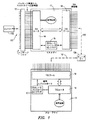
図1は、本研究の例示的な実施形態による積層された集積回路ダイを含むマルチチップパッケージを図式的に示している。マスタダイ11が、パッケージの外部端子(例えば、パッケージリード)に接続されている。1つまたは複数のスレーブダイが、マスタダイ11の上に積層可能である。(物理的積層を図1に示す図には明示していないが、当業者には認識されるであろう。)図1は、スレーブダイ12を明示しており、それは、マスタダイ11に物理的に対向して積み重なって位置決めされることになる。介在する積層されたスレーブダイ12を12Aにおいてまとめて示している。破線100は、マスタダイ11のTSVと、マスタダイ11に隣接するスレーブダイのそれぞれ軸方向に位置合わせされたTSVとの間の接続を示す。破線101は、スレーブダイ12のTSVと、スレーブダイ12に隣接するスレーブダイのそれぞれ軸方向に位置合わせされたTSVとの間の接続を示す。12Aにおける介在する積層されたスレーブダイの隣接するもの同士の間のTSV接続は、明示していない。集積回路ダイの積層をパッケージ化することが当技術分野においては知られており、隣接するダイの各対のそれぞれ軸方向に位置合わせされたTSVは、互いに電気的に接続されている。
FIG. 1 schematically illustrates a multi-chip package including stacked integrated circuit dies according to an exemplary embodiment of the present study. A master die 11 is connected to an external terminal (for example, package lead) of the package. One or more slave dies can be stacked on the master die 11. (The physical stackup is not explicitly shown in the diagram shown in FIG. 1, but will be recognized by those skilled in the art.) FIG. 1 clearly shows the slave die 12, which is physically attached to the master die 11. Is positioned so as to face each other. Intervening stacked slave dies 12 are shown collectively at 12A. Dashed
典型的には、いくつかのTSVは、各ダイ上に形成され、ダイを通って延在して、ダイのそれぞれ対向する側の隣接するダイのTSVに接続する。TSVのサブセットが、積み重なったダイ同士の間の信号および/または電力を接続するための設計によって選択される。本研究の例示的な実施形態は、チップ設計における使用のために配分されることも、不良TSVを交換するために使用されることもなかった残りの(スペア)TSVの利点を生かす。これらのスペアTSVは、将来、別の接続構成を確立するために利用可能にされる。 Typically, several TSVs are formed on each die and extend through the die and connect to TSVs of adjacent dies on each opposing side of the die. A subset of TSVs is selected by design to connect signals and / or power between stacked dies. The exemplary embodiment of this study takes advantage of the remaining (spare) TSVs that have not been allocated for use in chip design or used to replace defective TSVs. These spare TSVs will be made available to establish another connection configuration in the future.
図1におけるマスタダイ11は、パッケージ基板13(いくつかの実施形態においてはプリント回路基板)を介してパッケージ化されたマルチダイ積層部の外部端子に接続されている。マスタダイ11は、TSV18と、TSVルータ14と、TSVルータコントローラ15と、マスタダイ11の標準機能を実装する固有回路とを含む。スレーブダイ12は、TSV19と、TSVルータ14と、TSVルータコントローラ17と、それ自体の固有回路とを含む。
The master die 11 in FIG. 1 is connected to an external terminal of the multi-die stacked portion packaged through a package substrate 13 (a printed circuit board in some embodiments). The master die 11 includes a
図2は、本研究の例示的な実施形態によるTSVルータ14をより詳細に図式的に示している。ルータ14は、ダイのそれらのTSVに接続されているデフォルトポートを含み、それらのTSVは、積層されたマルチダイパッケージの意図された動作に必要な信号および電力を搬送するように、チップ設計によって割当て済みである。これらのTSVを、本明細書においてはデフォルトTSVとも呼ぶ。設計はまた、デフォルトTSVを配分して、ダイの対向する側の隣接するダイによって使用するため、ダイを通じて信号および/または電力を転送することが可能である。ルータ14は、ダイの固有回路とインターフェースするための固有回路ポートをさらに含む。元々製造されるダイの初期デフォルト構成においては、ルータ14は、デフォルトポートと固有回路ポートとの間の適切な接続を実装して、所望に応じてデフォルトTSVを固有回路に接続する。
FIG. 2 schematically illustrates the
この開示の目的のため、ルータが、スイッチ、マルチプレクサ、または複数の入力のうちのいずれか1つを出力ポートに選択的に接続するための当技術分野において知られている任意の他の手段を含むことに留意すべきである。 For the purposes of this disclosure, a router uses a switch, multiplexer, or any other means known in the art for selectively connecting any one of a plurality of inputs to an output port. It should be noted that it includes.
これまでは、残りのスペアTSVは、それらが製造プロセス中に識別された不良TSVを交換する冗長目的に利用可能な場合、初期の製造プロセス中を除いては使用されることはなかった。本研究によれば、ルータ14は、スペアTSVに接続されている再配分ポートを含む。したがって、これらのスペアTSVは、その標準ミッションモードでパッケージのフィールド動作中に、積層されたマルチダイパッケージ内で、接続を再構成し、かつ/または新規接続を構成する際に使用するために利用可能である。
Previously, the remaining spare TSVs were not used except during the initial manufacturing process if they were available for redundancy purposes to replace defective TSVs identified during the manufacturing process. According to this study,
図2はまた、様々な実施形態においては、ルータコントローラ(図1における15および17も参照のこと)が、ルータ14を介して(破線を参照のこと)、または専用接続部21によって、関連するダイのデフォルトTSVに接続可能であることを示している。コントローラ内のプログラマブルレジスタは、すでに別の形で接続されている信号を再接続または切断するため、または前に存在していなかった新規接続を形成するために、スペアTSVを配分するように、TSVを介してアクセス可能であり、22における制御接続部を介してルータ14を制御するために使用可能である。
FIG. 2 also relates in various embodiments that a router controller (see also 15 and 17 in FIG. 1) is associated via a router 14 (see dashed lines) or by a
図3は、マスタダイ11、および複数のスレーブダイ12(スレーブダイ1〜nとも示す)を示し、そのルータコントローラは、相互接続されたダイのTSVを含む専用リンクを介して相互接続されている。いくつかの実施形態においては、専用リンクは、マスタコントローラ15からそれぞれのスレーブコントローラ17に対して、それぞれ個別の接続の形態であってよい。これを、図3における破線の接続で示している。いくつかの実施形態においては、単一の並列リンクは、マスタコントローラを共有バス31に関してすべてのスレーブコントローラに接続する。個別コントローラ相互接続による破線の実施形態においては、マスタコントローラ15は、それぞれのスレーブコントローラ17につき1つのいくつかの個別ポートを有する。したがって、これらの実施形態は、その数のスレーブダイのみに適応する。一方では、共有バスの実施形態は、スレーブダイを識別するために存在するアドレスと同じスレーブダイに適応する。したがって、支持可能なスレーブダイの数は、共有のバス31によって支持されるデバイスアドレスフィールドの幅によってのみ決まる。
FIG. 3 shows a master die 11 and a plurality of slave dies 12 (also referred to as slave dies 1-n), whose router controllers are interconnected via dedicated links that include interconnected die TSVs. In some embodiments, the dedicated link may be in the form of a separate connection from the
いくつかの実施形態は、既存の接続を遮断し、かつ/または新規接続を形成することに対応する具体的な値により、関連するルータコントローラの1つまたは複数のレジスタをプログラミングすることによってダイのTSVを再配分する。概して、ユーザは、その接続値を積層内のダイ(例えば、マスタ)のルータコントローラのレジスタにプログラミングし、それは、ひいては、積層内の他のダイ内の対応するレジスタに影響をもたらす。このようにして、積層内のすべてのダイの中でTSV接続構成は調整可能である。 Some embodiments allow the die to be programmed by programming one or more registers of the associated router controller with specific values corresponding to blocking existing connections and / or creating new connections. Reallocate TSV. Generally, the user programs that connection value into the router controller register of a die (eg, master) in the stack, which in turn affects the corresponding register in the other die in the stack. In this way, the TSV connection configuration can be adjusted among all the dies in the stack.
再度図3を参照すると、いくつかの実施形態においては、ユーザは指定されたコマンドを利用して、外部コントローラ102からユーザコマンドを受け取るために103において外部パッケージリードに接続されている(図1も参照のこと)マスタダイ11上の適切なルータコントローラレジスタを再度プログラミングする。いくつかの実施形態においては、103における接続は、マスタダイ11のTSV、パッケージ基板、および外部パッケージ端子を介して行われる。マスタダイに関しては、固有回路は、ルータコントローラ15へのポート38を有し、その中のレジスタへの読出し/書込みアクセスに使用される。いくつかの実施形態においては、TSVコントローラ15は、TSVルータコントローラリンク(例えば、共有バス31)を使用して、その新規に書き込まれたレジスタ値(または、所望のTSV構成に必要な対応する値)を、TSV接続の所望の再構成で含まれる任意のスレーブダイ(または複数のダイ)のルータコントローラレジスタに複写する。マスタダイ11のルータコントローラ15は、コマンド内に含まれる情報から、そのレジスタと、影響されたスレーブダイコントローラ17のものとに書き込むべき適切な値を確定して、積層部の所望のTSV構成を実現する。
Referring again to FIG. 3, in some embodiments, a user is connected to an external package lead at 103 to receive a user command from the
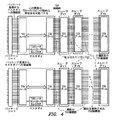
図4は、本研究の例示的な実施形態による既存の接続の再構成を示す。図4の上部は、製造時点で稼働中に全利用可能なTSVのサブセット(図4では、黒い稼働中TSV線で示す)を有する一層のダイを示している。ミッションモードで使用中の何らかのときに、ダイ積層部のスペアTSV接続は、図4の下部における(別の黒い稼働中TSV線で示す)元々の稼働中TSV以外のTSVを使用するように再構成可能である。概して、コマンドが、ルータコントローラのうちの1つまたは複数のレジスタをプログラミングするように発行され、次いでそれは、関連するTSVルータに、関連する接続を再度割当てさせる。これは、図5に示すなどの独自のコマンドを有するいくつかの実施形態において行われる。コマンドは、必須デバイスアドレス(DA)およびコマンド情報(CMD)を有する。いくつかの実施形態においては、レジスタは、図5aに関連して後述するように読出し可能であるか、または図5bに関連して後述するように書込み可能である。レジスタの書込み(プログラミング)動作に関しては、いくつかの実施形態は、レジスタアドレスと、それの対応する書込みデータとを対で供給する。ターゲットレジスタアドレスならびにデータを供給することによって、コントローラは、他の書込み可能なレジスタタイプに必要なレジスタ群におけるすべてのフィールドに対して、正確なデータを発行する必要がない。したがって、コントローラは、すべての既存のレジスタ値のマップを維持するか、または後続の再プログラミングのためのレジスタ値をまず読み出すかなどのオーバヘッドを回避する。 FIG. 4 shows the reconfiguration of an existing connection according to an exemplary embodiment of this study. The top of FIG. 4 shows a single layer die with a subset of all TSVs that are available in production at the time of manufacture (shown in FIG. 4 as black operating TSV lines). When in use in mission mode, the die stack spare TSV connection is reconfigured to use a TSV other than the original live TSV (indicated by another black live TSV line) at the bottom of Figure 4. Is possible. In general, a command is issued to program one or more registers of the router controller, which then causes the associated TSV router to reassign the associated connection. This is done in some embodiments with unique commands, such as shown in FIG. The command has a mandatory device address (DA) and command information (CMD). In some embodiments, the registers can be read as described below in connection with FIG. 5a or written as described below in connection with FIG. 5b. With respect to register write (programming) operations, some embodiments provide a register address and its corresponding write data in pairs. By supplying the target register address as well as data, the controller does not need to issue accurate data for every field in the registers that are required for other writable register types. Thus, the controller avoids overhead such as maintaining a map of all existing register values or first reading register values for subsequent reprogramming.
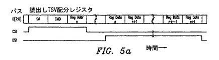
図5aは、本研究の例示的な実施形態によるTSV配分レジスタを読み出すために使用されるコマンドを示す。いくつかの実施形態においては、コマンドパケットは、従来のプロトコルに続く。具体的には、CSI(コマンドストローブ入力)が高いと、デバイスアドレスの後に、コマンドバイトが続き、レジスタアドレスバイトは、バス(例えば、図3の共有バス31)上へと駆動され、それによって、コマンドパケット内に与えられたアドレスにおいてレジスタから始まるTSV配分レジスタを読み出すようにターゲットデバイスを用意する。
FIG. 5a shows the command used to read the TSV distribution register according to an exemplary embodiment of the present study. In some embodiments, the command packet follows a conventional protocol. Specifically, when CSI (command strobe input) is high, the device address is followed by a command byte, and the register address byte is driven onto the bus (e.g., shared
所与の時間(典型的なデバイスデータシートにおいては、しばしばtCDSとも呼ぶ)が経過した後、コントローラは、コマンドパケットにおいて特定されたアドレスで始まる現在のレジスタデータによりバスを駆動するためにターゲットデバイスをシグナリングするDSI(データストローブ入力)をアサートする。ターゲットデバイスは、そのアドレスポインタを内部的に増分し、DSIが高い限り、またはレジスタアドレススペースの端部が到達されるまでの間、連続するレジスタアドレスからデータを送り出す。これは、コマンドへのダイの応答を構成し、DSIアサート後のバス活動によって示される。 After a given time (often referred to as tCDS in a typical device data sheet), the controller can target the target device to drive the bus with current register data starting at the address specified in the command packet. Assert DSI (data strobe input). The target device increments its address pointer internally and sends data from successive register addresses as long as the DSI is high or until the end of the register address space is reached. This constitutes the die's response to the command and is indicated by the bus activity after DSI assertion.
図5bは、本研究の例示的な実施形態によるマルチチップパッケージにおけるTSVの配分を変更するために使用されるコマンドパケットを示す。いくつかの実施形態においては、コマンドパケットは概して、図5aで示す従来のプロトコルの後に続き、デバイスアドレスを含み、コマンドバイトがその後に続き、アドレス/データのバイトの対がその後に続く。レジスタアドレスおよび対応するデータは、対で供給され、それぞれは、様々な実施形態においては、1バイトまたは複数バイトの長さであることが可能である。これらの詳細は、デバイス設計パラメータによって決まり、デバイスデータシートにおいて特定されることになる。例えば、より多いTSVを有するデバイスには、より少ないTSVを使用するデバイスよりも長いバイトカウントのアドレスフィールドおよびデータフィールドが必要な場合がある。それぞれのアドレスフィールドは、TSVへの信号の配分についての情報を含む配分レジスタの集合体における独自のレジストを示す。コマンドパケットデータフィールドにおいて供給されるデータは、特定の配分レジスタにおけるデータに上書きし、それによって、新規TSV/信号配分を実施する。 FIG. 5b shows a command packet used to change the allocation of TSVs in a multi-chip package according to an exemplary embodiment of this study. In some embodiments, the command packet generally follows the conventional protocol shown in FIG. 5a, includes the device address, followed by a command byte, followed by an address / data byte pair. Register addresses and corresponding data are provided in pairs, each of which can be one or more bytes long in various embodiments. These details depend on device design parameters and will be specified in the device data sheet. For example, a device with more TSVs may require a longer byte count address and data field than a device using fewer TSVs. Each address field indicates a unique register in the collection of distribution registers that contains information about the distribution of signals to the TSV. The data supplied in the command packet data field overwrites the data in a specific distribution register, thereby implementing a new TSV / signal distribution.
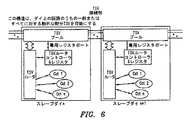
これまで未接続の固有ダイ回路を接続するための例示的な実施形態を図6に図式的に示している。TSVは、デフォルト製造構成で接続されなかった(Cct1-Cctnと概して示す)積層パッケージサブ回路内に接続するためにか、またはデフォルト製造構成で接続された積層パッケージ選択のサブ回路から切断するために使用可能である。 An exemplary embodiment for connecting previously unconnected unique die circuits is shown schematically in FIG. TSV to connect in a stacked package subcircuit that was not connected in the default manufacturing configuration (generally indicated as Cct1-Cctn) or to disconnect from a stacked package selection subcircuit connected in the default manufacturing configuration It can be used.
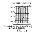
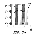
図7は、本研究の例示的な実施形態によるダイを追加し/ダイを積層から取り除く、またはダイを追加し/ダイをリングアーキテクチャから取り除くことを図式的に示している。一例としては、積層されたメモリパッケージが、メモリインターフェースまたはリングアーキテクチャから取り除かれたそのダイのうちの1つを有しても、または将来、インターフェース/リングに追加可能な「スペア」ダイを含んでもよい。図7におけるダイ0は、マスタダイ11であってよく、残りのダイ(Die1〜Die3)は、スレーブダイ12である。図7は、上部(図7b)、または中間部(図7c)のダイが、図7aのインターフェース/リング構成から取り除かれている状況を示している。いくつかの実施形態においては、ユーザは、適切なコマンドを発行するように外部コントローラ102(図1および図3も参照のこと)を動作させ、そのコマンドは、影響されたダイのTSVルータに、ダイの現在のTSV構成を、現在の構成で固有回路に接続されているダイのTSVのうちのダイ選択のものの固有回路から切断することによって変更させる。いくつかの実施形態においては、外部コントローラ102は、OS(オペレーティングシステム)に、またはパッケージにおける所定の状態を検出するコントローラのマイクロコードに自動的に応答してコマンドを発行する。
FIG. 7 schematically illustrates adding a die / removing a die from a stack or adding a die / removing a die from a ring architecture according to an exemplary embodiment of the present study. As an example, a stacked memory package may have one of its dies removed from the memory interface or ring architecture, or may include a “spare” die that can be added to the interface / ring in the future. Good. The die 0 in FIG. 7 may be the master die 11, and the remaining dies (
図8aは、本研究の例示的な実施形態によるデバイス積層部を示し、それは、ユーザか、または自動ソフトウェア/ハードウェア制御かのいずれかによって選択的に接続可能な「スペア」ダイ(ダイ3)を含む。例示的なアプリケーションが、1つまたは複数のスペアフラッシュダイを含むマルチチップパッケージフラッシュメモリデバイスにある。より大きなメモリ容量が求められる場合、スペアダイは、図8bに示すインターフェース/リング内に追加可能である。別の例としては、図8における1つのダイが故障した場合、それは、取り除くことが可能であり、スペアダイと交換可能であり、それによって、最終的には図7cに示す構成に到達し、マルチチップパッケージの有用寿命を延長する。様々な実施形態においては、ダイ交換プロセスは、特定のダイ上のエラーが及ぼすいくつかの閾値によってか、ダイ上の固有回路内の所定の数のサブ回路の故障によってか、または具体的なサブ回路の故障によって、トリガ可能である。その状態が検出されると、適切なコマンド(複数のコマンド)が、スペアダイのTSVルータコントローラに、および故障したダイに、適切な救済的な手順、例えば:(1)インターフェース/リング内にスペアダイを接続する、(2)故障ダイからスペアダイにデータを転送する、および(3)フィールドダイをインターフェース/リングから切断する、の実行に関与させる。 FIG. 8a shows a device stack according to an exemplary embodiment of the present study, which is a “spare” die (die 3) that can be selectively connected either by the user or by automatic software / hardware control including. An exemplary application is in a multi-chip package flash memory device that includes one or more spare flash dies. If larger memory capacity is required, spare dies can be added in the interface / ring shown in FIG. 8b. As another example, if one die in FIG. 8 fails, it can be removed and replaced with a spare die, thereby eventually reaching the configuration shown in FIG. Extend the useful life of chip packages. In various embodiments, the die replacement process may be due to some threshold of error on a particular die, due to the failure of a predetermined number of subcircuits in the unique circuitry on the die, or to a specific sub- Can be triggered by a circuit failure. When that condition is detected, the appropriate command (s) are sent to the spare die TSV router controller, and to the failed die, with appropriate remedy procedures, e.g .: (1) Spare die in interface / ring Participate in performing (2) transferring data from the failed die to the spare die, and (3) disconnecting the field die from the interface / ring.
図9は、本研究の例示的な実施形態によるシステムを図式的に示している。マルチダイ積層パッケージ91、例えば、図1〜図8bに関連して上述済みなどのパッケージは、外部電子回路92と通じるために結合されている。いくつかの実施形態においては、パッケージ91は、データ保存機能、例えば、フラッシュメモリ機能を実装する。いくつかの実施形態においては、パッケージ91は、任意の所望のアプリケーションの具体的な機能、例えば、デジタルデータ処理を実装する。様々な実施形態においては、電子回路92は、パッケージ91、例えば、パッケージ91によって実装されるデータ保存機能と協働することが可能なメモリコントローラによって実装される機能を使用し、かつ/または制御する回路のいずれの集合体であってよく、図1〜図8に関連して上述したコントローラ102の機能を実装することが可能である。
FIG. 9 schematically shows a system according to an exemplary embodiment of the present study. Multi-die
例示的な実施形態を詳細に前述してきたが、これは、本発明の範囲を限定するものでなく、様々な実施形態において実施可能である。 While exemplary embodiments have been described in detail above, this is not intended to limit the scope of the invention and can be implemented in various embodiments.
11 マスタダイ
12 スレーブダイ
12A スレーブダイ
13 パッケージ基板
14 TSVルータ
15 TSVルータコントローラ
17 TSVルータコントローラ
18 TSV
19 TSV
21 専用接続部
22 制御接続部
31 共有バス
38 ポート
91 マルチダイ積層パッケージ
92 外部電子回路
100 破線
101 破線
102 外部コントローラ
103 接続
11 Master die
12 Slave die
12A Slave die
13 Package substrate
14 TSV router
15 TSV router controller
17 TSV router controller
18 TSV
19 TSV
21 Dedicated connection
22 Control connection
31 Shared bus
38 ports
91 Multi-die stacked package
92 External electronics
100 dashed line
101 Dashed line
102 External controller
103 Connection
Claims (26)
前記ダイに対する信号に外部アクセスを供給するための、前記ダイを通って延在する第1の複数のビアと、
前記第1の複数のビアに、複数の信号搬送構成のうちの選択された1つをとらせるように構成されている、前記ビアと結合されているルータとを
備え、
前記選択された信号搬送構成においては、少なくとも1つのビアは、前記少なくとも1つのビアが、別の前記信号搬送構成では搬送しない少なくとも1つの信号を搬送する、
ダイ。 An integrated circuit die,
A first plurality of vias extending through the die for providing external access to signals to the die;
A router coupled to the via configured to cause the first plurality of vias to take a selected one of a plurality of signal transport configurations; and
In the selected signal carrying configuration, at least one via carries at least one signal that the at least one via does not carry in another signal carrying configuration;
Die.
前記複数のビアに、前記ルータを使用して第2の信号搬送構成をとらせるステップと
を含み、
前記第1の信号搬送構成においては、前記ビアのうちの少なくとも1つは、前記少なくとも1つのビアが、前記第2の信号搬送構成では搬送しない関連する少なくとも1つの信号を搬送する、
集積回路ダイ動作の方法。 Having a plurality of vias extending through the die and providing external access to signals for the die to take a first signal transport configuration using a router;
Allowing the plurality of vias to adopt a second signal transport configuration using the router;
In the first signal carrying configuration, at least one of the vias carries at least one associated signal that the at least one via does not carry in the second signal carrying configuration;
Method of integrated circuit die operation.
それぞれのダイは、
前記ダイに対する信号に外部アクセスを供給するための、前記ダイを通って延在する複数のビアであって、前記複数のダイは、それぞれのダイの前記ビアが、隣接するダイの前記ビアに接続されるように、積み重なって配置されている、ビアと、
前記関連するビアと結合され、前記関連するビアに、前記ダイの固有回路が、前記関連するビアのうちの選択されたものによって接続されて、隣接するダイとシグナリングするシグナリング接続構成をとらせるように、および
前記関連するビアに、前記ダイの前記固有回路が接続されずに、前記隣接するダイとシグナリングするシグナリング切断構成をとらせるように構成されているルータとを含む、
積層された集積回路装置。 In a stacked integrated circuit device comprising a plurality of integrated circuit dies,
Each die is
A plurality of vias extending through the die for providing external access to signals to the die, wherein the plurality of dies connect the vias of each die to the vias of adjacent dies; Vias, arranged in stacks, as
Coupled to the associated vias, causing the associated vias to be connected by a selected one of the associated vias to have a signaling connection configuration that signals with adjacent dies And a router configured to cause the associated via to have a signaling disconnect configuration for signaling with the adjacent die without being connected to the specific circuitry of the die.
Stacked integrated circuit device.
前記複数のダイは、それぞれのダイの前記ビアが、隣接するダイの前記ビアに接続されるように積み重なって配置されている、
積層された集積回路装置。 Comprising a plurality of integrated circuit dies according to claim 1;
The plurality of dies are arranged in a stack such that the vias of each die are connected to the vias of adjacent dies,
Stacked integrated circuit device.
少なくとも1つのダイの前記ビアに、前記少なくとも1つのダイの固有回路が、前記ビアのうちの選択されたものによって接続されて、隣接するダイとシグナリングするシグナリング接続構成をとらせるステップと、
前記少なくとも1つのダイの前記ビアに、前記少なくとも1つのダイの前記固有回路が接続されずに、前記隣接するダイとシグナリングするシグナリング切断構成をとらせるステップと
を含む、方法。 A method of operating a plurality of stacked integrated circuit dies, each die including a plurality of vias extending therethrough for providing external access to signals to the die, each die The vias are connected to the vias of adjacent dies,
Causing the vias of at least one die to have a signaling connection configuration in which the unique circuitry of the at least one die is connected by a selected one of the vias and signaling with an adjacent die;
Allowing the vias of the at least one die to have a signaling disconnect configuration for signaling with the adjacent dies without being connected to the unique circuitry of the at least one die.
前記積層された集積回路装置の外部に設けられ、それと結合されて、それと通じる電子回路と
を備える、システム。 The stacked integrated circuit device according to claim 17,
A system comprising: an electronic circuit provided outside the stacked integrated circuit device, coupled to and connected to the integrated circuit device.
前記積層された集積回路装置の外部に設けられ、それと結合されて、それと通じる電子回路と
を備える、システム。 The stacked integrated circuit device according to claim 15,
A system comprising: an electronic circuit provided outside the stacked integrated circuit device, coupled to and connected to the integrated circuit device.
Applications Claiming Priority (5)
| Application Number | Priority Date | Filing Date | Title |
|---|---|---|---|
| US25286509P | 2009-10-19 | 2009-10-19 | |
| US61/252,865 | 2009-10-19 | ||
| US12/773,340 | 2010-05-04 | ||
| US12/773,340 US8604593B2 (en) | 2009-10-19 | 2010-05-04 | Reconfiguring through silicon vias in stacked multi-die packages |
| PCT/CA2010/001650 WO2011047470A1 (en) | 2009-10-19 | 2010-10-19 | Reconfiguring through silicon vias in stacked multi-die packages |
Publications (2)
| Publication Number | Publication Date |
|---|---|
| JP2013508941A true JP2013508941A (en) | 2013-03-07 |
| JP2013508941A5 JP2013508941A5 (en) | 2013-11-28 |
Family
ID=43878833
Family Applications (1)
| Application Number | Title | Priority Date | Filing Date |
|---|---|---|---|
| JP2012533445A Pending JP2013508941A (en) | 2009-10-19 | 2010-10-19 | Reconfiguration of through-silicon vias in stacked multi-die packages |
Country Status (7)
| Country | Link |
|---|---|
| US (2) | US8604593B2 (en) |
| EP (1) | EP2491589A4 (en) |
| JP (1) | JP2013508941A (en) |
| KR (1) | KR20120085650A (en) |
| CN (1) | CN102227806A (en) |
| TW (1) | TWI476889B (en) |
| WO (1) | WO2011047470A1 (en) |
Cited By (1)
| Publication number | Priority date | Publication date | Assignee | Title |
|---|---|---|---|---|
| JP2012142576A (en) * | 2010-12-28 | 2012-07-26 | Samsung Electronics Co Ltd | Laminate structured semiconductor device having through electrode, semiconductor memory device, semiconductor memory/system, and operation method of the semiconductor memory/system |
Families Citing this family (29)
| Publication number | Priority date | Publication date | Assignee | Title |
|---|---|---|---|---|
| US9229887B2 (en) * | 2008-02-19 | 2016-01-05 | Micron Technology, Inc. | Memory device with network on chip methods, apparatus, and systems |
| US7978721B2 (en) | 2008-07-02 | 2011-07-12 | Micron Technology Inc. | Multi-serial interface stacked-die memory architecture |
| US8086913B2 (en) | 2008-09-11 | 2011-12-27 | Micron Technology, Inc. | Methods, apparatus, and systems to repair memory |
| US9123552B2 (en) * | 2010-03-30 | 2015-09-01 | Micron Technology, Inc. | Apparatuses enabling concurrent communication between an interface die and a plurality of dice stacks, interleaved conductive paths in stacked devices, and methods for forming and operating the same |
| US8362602B2 (en) * | 2010-08-09 | 2013-01-29 | Headway Technologies, Inc. | Layered chip package and method of manufacturing same |
| US8916910B2 (en) * | 2010-12-13 | 2014-12-23 | Research Foundation Of State University Of New York | Reconfigurable RF/digital hybrid 3D interconnect |
| KR101208962B1 (en) * | 2011-02-22 | 2012-12-06 | 에스케이하이닉스 주식회사 | Semiconductor apparatus |
| US8624626B2 (en) | 2011-11-14 | 2014-01-07 | Taiwan Semiconductor Manufacturing Co., Ltd. | 3D IC structure and method |
| US20130159587A1 (en) * | 2011-12-15 | 2013-06-20 | Aaron Nygren | Interconnect Redundancy for Multi-Interconnect Device |
| US8933715B2 (en) | 2012-04-08 | 2015-01-13 | Elm Technology Corporation | Configurable vertical integration |
| US9448947B2 (en) * | 2012-06-01 | 2016-09-20 | Qualcomm Incorporated | Inter-chip memory interface structure |
| US9478502B2 (en) * | 2012-07-26 | 2016-10-25 | Micron Technology, Inc. | Device identification assignment and total device number detection |
| US9026872B2 (en) * | 2012-08-16 | 2015-05-05 | Xilinx, Inc. | Flexible sized die for use in multi-die integrated circuit |
| KR102190382B1 (en) | 2012-12-20 | 2020-12-11 | 삼성전자주식회사 | Semiconductor package |
| KR102058101B1 (en) * | 2012-12-20 | 2019-12-20 | 에스케이하이닉스 주식회사 | Semiconductor integrated circuit |
| US9612988B2 (en) * | 2013-07-23 | 2017-04-04 | International Business Machines Corporation | Donor cores to improve integrated circuit yield |
| US20150155039A1 (en) * | 2013-12-02 | 2015-06-04 | Silicon Storage Technology, Inc. | Three-Dimensional Flash NOR Memory System With Configurable Pins |
| US9245825B2 (en) | 2014-01-23 | 2016-01-26 | Sandisk Technologies Inc. | I/O pin capacitance reduction using TSVS |
| US9501603B2 (en) | 2014-09-05 | 2016-11-22 | International Business Machines Corporation | Integrated circuit design changes using through-silicon vias |
| US10002653B2 (en) | 2014-10-28 | 2018-06-19 | Nxp Usa, Inc. | Die stack address bus having a programmable width |
| KR102290020B1 (en) * | 2015-06-05 | 2021-08-19 | 삼성전자주식회사 | Semiconductor memory device providing analiysis and relief of soft data fail in stacked chips |
| US9871020B1 (en) * | 2016-07-14 | 2018-01-16 | Globalfoundries Inc. | Through silicon via sharing in a 3D integrated circuit |
| US10249590B2 (en) | 2017-06-06 | 2019-04-02 | Globalfoundries Inc. | Stacked dies using one or more interposers |
| US11055167B2 (en) * | 2018-05-14 | 2021-07-06 | Micron Technology, Inc. | Channel-scope proximity disturb and defect remapping scheme for non-volatile memory |
| US10838831B2 (en) * | 2018-05-14 | 2020-11-17 | Micron Technology, Inc. | Die-scope proximity disturb and defect remapping scheme for non-volatile memory |
| US11048597B2 (en) * | 2018-05-14 | 2021-06-29 | Micron Technology, Inc. | Memory die remapping |
| CN112102862B (en) * | 2020-09-22 | 2023-03-07 | 武汉新芯集成电路制造有限公司 | Chip structure, data reading processing method and chip structure manufacturing method |
| US11226767B1 (en) * | 2020-09-30 | 2022-01-18 | Micron Technology, Inc. | Apparatus with access control mechanism and methods for operating the same |
| US11468945B2 (en) * | 2020-10-15 | 2022-10-11 | Arm Limited | 3D storage architecture with tier-specific controls |
Citations (2)
| Publication number | Priority date | Publication date | Assignee | Title |
|---|---|---|---|---|
| US20090015322A1 (en) * | 2007-07-11 | 2009-01-15 | Arm Limited | Integrated circuit with multiple layers of circuits |
| WO2009079772A1 (en) * | 2007-12-20 | 2009-07-02 | Mosaid Technologies Incorporated | Method for stacking serially-connected integrated circuits and multi-chip device made from same |
Family Cites Families (17)
| Publication number | Priority date | Publication date | Assignee | Title |
|---|---|---|---|---|
| TW511414B (en) | 2001-04-19 | 2002-11-21 | Via Tech Inc | Data processing system and method, and control chip, and printed circuit board thereof |
| US20030040166A1 (en) | 2001-05-25 | 2003-02-27 | Mark Moshayedi | Apparatus and method for stacking integrated circuits |
| DE102004045527B4 (en) * | 2003-10-08 | 2009-12-03 | Siemens Ag | Configurable logic circuitry |
| JP4708176B2 (en) * | 2005-12-08 | 2011-06-22 | エルピーダメモリ株式会社 | Semiconductor device |
| US7352602B2 (en) * | 2005-12-30 | 2008-04-01 | Micron Technology, Inc. | Configurable inputs and outputs for memory stacking system and method |
| US20070220207A1 (en) * | 2006-03-14 | 2007-09-20 | Bryan Black | Transferring data from stacked memory |
| TWI332239B (en) * | 2006-12-14 | 2010-10-21 | United Microelectronics Corp | Semiconductor wafer and method for forming the same |
| KR100871381B1 (en) * | 2007-06-20 | 2008-12-02 | 주식회사 하이닉스반도체 | Through silicon via chip stack package |
| US8136071B2 (en) | 2007-09-12 | 2012-03-13 | Neal Solomon | Three dimensional integrated circuits and methods of fabrication |
| US20090072373A1 (en) * | 2007-09-14 | 2009-03-19 | Reynaldo Corpuz Javier | Packaged integrated circuits and methods to form a stacked integrated circuit package |
| US7816934B2 (en) * | 2007-10-16 | 2010-10-19 | Micron Technology, Inc. | Reconfigurable connections for stacked semiconductor devices |
| KR101176187B1 (en) | 2007-11-21 | 2012-08-22 | 삼성전자주식회사 | Stacked semiconductor device and method for thereof serial path build up |
| US8384417B2 (en) * | 2008-09-10 | 2013-02-26 | Qualcomm Incorporated | Systems and methods utilizing redundancy in semiconductor chip interconnects |
| US7796446B2 (en) * | 2008-09-19 | 2010-09-14 | Qimonda Ag | Memory dies for flexible use and method for configuring memory dies |
| US8134852B2 (en) * | 2008-10-14 | 2012-03-13 | Mosaid Technologies Incorporated | Bridge device architecture for connecting discrete memory devices to a system |
| US8472199B2 (en) * | 2008-11-13 | 2013-06-25 | Mosaid Technologies Incorporated | System including a plurality of encapsulated semiconductor chips |
| US8977809B2 (en) * | 2008-11-26 | 2015-03-10 | Micron Technology, Inc. | Sharing resources in multi-dice stacks |
-
2010
- 2010-05-04 US US12/773,340 patent/US8604593B2/en active Active
- 2010-08-26 TW TW099128670A patent/TWI476889B/en not_active IP Right Cessation
- 2010-10-19 EP EP10824345.2A patent/EP2491589A4/en not_active Withdrawn
- 2010-10-19 JP JP2012533445A patent/JP2013508941A/en active Pending
- 2010-10-19 WO PCT/CA2010/001650 patent/WO2011047470A1/en active Application Filing
- 2010-10-19 KR KR1020117011810A patent/KR20120085650A/en not_active Application Discontinuation
- 2010-10-19 CN CN201080003433.2A patent/CN102227806A/en active Pending
-
2013
- 2013-12-10 US US14/101,507 patent/US9117685B2/en active Active
Patent Citations (2)
| Publication number | Priority date | Publication date | Assignee | Title |
|---|---|---|---|---|
| US20090015322A1 (en) * | 2007-07-11 | 2009-01-15 | Arm Limited | Integrated circuit with multiple layers of circuits |
| WO2009079772A1 (en) * | 2007-12-20 | 2009-07-02 | Mosaid Technologies Incorporated | Method for stacking serially-connected integrated circuits and multi-chip device made from same |
Cited By (1)
| Publication number | Priority date | Publication date | Assignee | Title |
|---|---|---|---|---|
| JP2012142576A (en) * | 2010-12-28 | 2012-07-26 | Samsung Electronics Co Ltd | Laminate structured semiconductor device having through electrode, semiconductor memory device, semiconductor memory/system, and operation method of the semiconductor memory/system |
Also Published As
| Publication number | Publication date |
|---|---|
| US8604593B2 (en) | 2013-12-10 |
| TW201126682A (en) | 2011-08-01 |
| US9117685B2 (en) | 2015-08-25 |
| WO2011047470A1 (en) | 2011-04-28 |
| US20140097891A1 (en) | 2014-04-10 |
| TWI476889B (en) | 2015-03-11 |
| KR20120085650A (en) | 2012-08-01 |
| US20110090004A1 (en) | 2011-04-21 |
| CN102227806A (en) | 2011-10-26 |
| EP2491589A4 (en) | 2015-07-22 |
| EP2491589A1 (en) | 2012-08-29 |
Similar Documents
| Publication | Publication Date | Title |
|---|---|---|
| JP2013508941A (en) | Reconfiguration of through-silicon vias in stacked multi-die packages | |
| US9780073B2 (en) | Using interrupted through-silicon-vias in integrated circuits adapted for stacking | |
| CN105679748B (en) | Method and apparatus for testing accessory in multi-chip encapsulation body | |
| US11194757B2 (en) | Scalable 2.5D interface circuitry | |
| US8630287B2 (en) | Multiple core network device with core redundancy | |
| TW201209842A (en) | 3D semiconductor device | |
| US10346325B2 (en) | Ring bus architecture for use in a memory module | |
| US9373384B2 (en) | Integrated circuit device having programmable input capacitance | |
| CN107704285A (en) | Field programmable gate array multi version configuration chip, system and method | |
| US9466555B2 (en) | Semiconductor chip and stack type semiconductor apparatus using the same | |
| US11169945B1 (en) | Bridge supporting multiple interfaces access to subsystem | |
| US20150039813A1 (en) | NAND Interface Capacity Extender Device For Extending Solid State Drives Capacity, Performance, And Reliability | |
| US7920433B2 (en) | Method and apparatus for storage device with a logic unit and method for manufacturing same | |
| US20150160890A1 (en) | Memory multi-chip package (mcp) with integral bus splitter | |
| US10565143B2 (en) | Circuitry to alleviate printed circuit board routing congestion | |
| US20100135153A1 (en) | Redundant signal transmission | |
| CN117690462A (en) | Tightly coupled random access memory interface interposer die |
Legal Events
| Date | Code | Title | Description |
|---|---|---|---|
| A521 | Written amendment |
Free format text: JAPANESE INTERMEDIATE CODE: A523 Effective date: 20131009 |
|
| A621 | Written request for application examination |
Free format text: JAPANESE INTERMEDIATE CODE: A621 Effective date: 20131009 |
|
| A871 | Explanation of circumstances concerning accelerated examination |
Free format text: JAPANESE INTERMEDIATE CODE: A871 Effective date: 20131009 |
|
| A975 | Report on accelerated examination |
Free format text: JAPANESE INTERMEDIATE CODE: A971005 Effective date: 20131204 |
|
| A131 | Notification of reasons for refusal |
Free format text: JAPANESE INTERMEDIATE CODE: A131 Effective date: 20131210 |
|
| A02 | Decision of refusal |
Free format text: JAPANESE INTERMEDIATE CODE: A02 Effective date: 20140609 |
|
| RD03 | Notification of appointment of power of attorney |
Free format text: JAPANESE INTERMEDIATE CODE: A7423 Effective date: 20140926 |
|
| RD04 | Notification of resignation of power of attorney |
Free format text: JAPANESE INTERMEDIATE CODE: A7424 Effective date: 20150428 |
|
| RD03 | Notification of appointment of power of attorney |
Free format text: JAPANESE INTERMEDIATE CODE: A7423 Effective date: 20150701 |