KR20120030404A - Light source comprising a light emitter arranged inside a translucent outer envelope - Google Patents
Light source comprising a light emitter arranged inside a translucent outer envelope Download PDFInfo
- Publication number
- KR20120030404A KR20120030404A KR1020117028885A KR20117028885A KR20120030404A KR 20120030404 A KR20120030404 A KR 20120030404A KR 1020117028885 A KR1020117028885 A KR 1020117028885A KR 20117028885 A KR20117028885 A KR 20117028885A KR 20120030404 A KR20120030404 A KR 20120030404A
- Authority
- KR
- South Korea
- Prior art keywords
- light
- envelope
- light emitting
- inner envelope
- light source
- Prior art date
Links
- 239000000463 material Substances 0.000 claims description 90
- 238000009826 distribution Methods 0.000 claims description 48
- 238000001816 cooling Methods 0.000 claims description 22
- 238000009792 diffusion process Methods 0.000 claims description 18
- 239000006185 dispersion Substances 0.000 claims description 12
- 230000005855 radiation Effects 0.000 claims description 4
- 240000003380 Passiflora rubra Species 0.000 claims description 2
- 238000000034 method Methods 0.000 claims 20
- 230000000694 effects Effects 0.000 abstract description 13
- 230000001965 increasing effect Effects 0.000 abstract description 9
- OAICVXFJPJFONN-UHFFFAOYSA-N Phosphorus Chemical compound [P] OAICVXFJPJFONN-UHFFFAOYSA-N 0.000 description 17
- 230000003287 optical effect Effects 0.000 description 11
- 239000000203 mixture Substances 0.000 description 9
- 239000003086 colorant Substances 0.000 description 7
- 238000001228 spectrum Methods 0.000 description 7
- 238000006243 chemical reaction Methods 0.000 description 6
- 238000004519 manufacturing process Methods 0.000 description 6
- 229920000515 polycarbonate Polymers 0.000 description 6
- 239000004417 polycarbonate Substances 0.000 description 6
- 239000002223 garnet Substances 0.000 description 5
- 238000005286 illumination Methods 0.000 description 5
- 229910018072 Al 2 O 3 Inorganic materials 0.000 description 4
- 229910004298 SiO 2 Inorganic materials 0.000 description 4
- 229910010413 TiO 2 Inorganic materials 0.000 description 4
- 239000011521 glass Substances 0.000 description 4
- 229920000642 polymer Polymers 0.000 description 4
- 229920002379 silicone rubber Polymers 0.000 description 4
- 239000004945 silicone rubber Substances 0.000 description 4
- 238000000576 coating method Methods 0.000 description 3
- 238000000295 emission spectrum Methods 0.000 description 3
- 238000001746 injection moulding Methods 0.000 description 3
- 239000011159 matrix material Substances 0.000 description 3
- 150000004767 nitrides Chemical class 0.000 description 3
- 230000003595 spectral effect Effects 0.000 description 3
- 238000004804 winding Methods 0.000 description 3
- 239000011248 coating agent Substances 0.000 description 2
- 239000000110 cooling liquid Substances 0.000 description 2
- 230000004907 flux Effects 0.000 description 2
- 230000005484 gravity Effects 0.000 description 2
- 239000004033 plastic Substances 0.000 description 2
- 238000005507 spraying Methods 0.000 description 2
- MCSXGCZMEPXKIW-UHFFFAOYSA-N 3-hydroxy-4-[(4-methyl-2-nitrophenyl)diazenyl]-N-(3-nitrophenyl)naphthalene-2-carboxamide Chemical compound Cc1ccc(N=Nc2c(O)c(cc3ccccc23)C(=O)Nc2cccc(c2)[N+]([O-])=O)c(c1)[N+]([O-])=O MCSXGCZMEPXKIW-UHFFFAOYSA-N 0.000 description 1
- 229920000742 Cotton Polymers 0.000 description 1
- 238000010521 absorption reaction Methods 0.000 description 1
- 230000002457 bidirectional effect Effects 0.000 description 1
- 230000005540 biological transmission Effects 0.000 description 1
- 239000003795 chemical substances by application Substances 0.000 description 1
- 238000000748 compression moulding Methods 0.000 description 1
- 239000012809 cooling fluid Substances 0.000 description 1
- 230000007812 deficiency Effects 0.000 description 1
- 230000001419 dependent effect Effects 0.000 description 1
- 230000003028 elevating effect Effects 0.000 description 1
- 238000005530 etching Methods 0.000 description 1
- 230000005284 excitation Effects 0.000 description 1
- 239000012530 fluid Substances 0.000 description 1
- 238000010438 heat treatment Methods 0.000 description 1
- 238000010102 injection blow moulding Methods 0.000 description 1
- 238000002156 mixing Methods 0.000 description 1
- 238000000465 moulding Methods 0.000 description 1
- 238000013021 overheating Methods 0.000 description 1
- 239000002245 particle Substances 0.000 description 1
- 229910052698 phosphorus Inorganic materials 0.000 description 1
- 239000011574 phosphorus Substances 0.000 description 1
- 238000010791 quenching Methods 0.000 description 1
- 230000000171 quenching effect Effects 0.000 description 1
- 238000005488 sandblasting Methods 0.000 description 1
- 229920006395 saturated elastomer Polymers 0.000 description 1
- 239000000126 substance Substances 0.000 description 1
- 239000000758 substrate Substances 0.000 description 1
Images


Classifications
-
- F—MECHANICAL ENGINEERING; LIGHTING; HEATING; WEAPONS; BLASTING
- F21—LIGHTING
- F21V—FUNCTIONAL FEATURES OR DETAILS OF LIGHTING DEVICES OR SYSTEMS THEREOF; STRUCTURAL COMBINATIONS OF LIGHTING DEVICES WITH OTHER ARTICLES, NOT OTHERWISE PROVIDED FOR
- F21V3/00—Globes; Bowls; Cover glasses
- F21V3/04—Globes; Bowls; Cover glasses characterised by materials, surface treatments or coatings
- F21V3/10—Globes; Bowls; Cover glasses characterised by materials, surface treatments or coatings characterised by coatings
- F21V3/12—Globes; Bowls; Cover glasses characterised by materials, surface treatments or coatings characterised by coatings the coatings comprising photoluminescent substances
-
- F—MECHANICAL ENGINEERING; LIGHTING; HEATING; WEAPONS; BLASTING
- F21—LIGHTING
- F21K—NON-ELECTRIC LIGHT SOURCES USING LUMINESCENCE; LIGHT SOURCES USING ELECTROCHEMILUMINESCENCE; LIGHT SOURCES USING CHARGES OF COMBUSTIBLE MATERIAL; LIGHT SOURCES USING SEMICONDUCTOR DEVICES AS LIGHT-GENERATING ELEMENTS; LIGHT SOURCES NOT OTHERWISE PROVIDED FOR
- F21K9/00—Light sources using semiconductor devices as light-generating elements, e.g. using light-emitting diodes [LED] or lasers
- F21K9/20—Light sources comprising attachment means
- F21K9/23—Retrofit light sources for lighting devices with a single fitting for each light source, e.g. for substitution of incandescent lamps with bayonet or threaded fittings
- F21K9/232—Retrofit light sources for lighting devices with a single fitting for each light source, e.g. for substitution of incandescent lamps with bayonet or threaded fittings specially adapted for generating an essentially omnidirectional light distribution, e.g. with a glass bulb
-
- F—MECHANICAL ENGINEERING; LIGHTING; HEATING; WEAPONS; BLASTING
- F21—LIGHTING
- F21K—NON-ELECTRIC LIGHT SOURCES USING LUMINESCENCE; LIGHT SOURCES USING ELECTROCHEMILUMINESCENCE; LIGHT SOURCES USING CHARGES OF COMBUSTIBLE MATERIAL; LIGHT SOURCES USING SEMICONDUCTOR DEVICES AS LIGHT-GENERATING ELEMENTS; LIGHT SOURCES NOT OTHERWISE PROVIDED FOR
- F21K9/00—Light sources using semiconductor devices as light-generating elements, e.g. using light-emitting diodes [LED] or lasers
- F21K9/60—Optical arrangements integrated in the light source, e.g. for improving the colour rendering index or the light extraction
- F21K9/64—Optical arrangements integrated in the light source, e.g. for improving the colour rendering index or the light extraction using wavelength conversion means distinct or spaced from the light-generating element, e.g. a remote phosphor layer
-
- F—MECHANICAL ENGINEERING; LIGHTING; HEATING; WEAPONS; BLASTING
- F21—LIGHTING
- F21K—NON-ELECTRIC LIGHT SOURCES USING LUMINESCENCE; LIGHT SOURCES USING ELECTROCHEMILUMINESCENCE; LIGHT SOURCES USING CHARGES OF COMBUSTIBLE MATERIAL; LIGHT SOURCES USING SEMICONDUCTOR DEVICES AS LIGHT-GENERATING ELEMENTS; LIGHT SOURCES NOT OTHERWISE PROVIDED FOR
- F21K9/00—Light sources using semiconductor devices as light-generating elements, e.g. using light-emitting diodes [LED] or lasers
- F21K9/60—Optical arrangements integrated in the light source, e.g. for improving the colour rendering index or the light extraction
- F21K9/65—Optical arrangements integrated in the light source, e.g. for improving the colour rendering index or the light extraction specially adapted for changing the characteristics or the distribution of the light, e.g. by adjustment of parts
-
- F—MECHANICAL ENGINEERING; LIGHTING; HEATING; WEAPONS; BLASTING
- F21—LIGHTING
- F21V—FUNCTIONAL FEATURES OR DETAILS OF LIGHTING DEVICES OR SYSTEMS THEREOF; STRUCTURAL COMBINATIONS OF LIGHTING DEVICES WITH OTHER ARTICLES, NOT OTHERWISE PROVIDED FOR
- F21V3/00—Globes; Bowls; Cover glasses
-
- F—MECHANICAL ENGINEERING; LIGHTING; HEATING; WEAPONS; BLASTING
- F21—LIGHTING
- F21V—FUNCTIONAL FEATURES OR DETAILS OF LIGHTING DEVICES OR SYSTEMS THEREOF; STRUCTURAL COMBINATIONS OF LIGHTING DEVICES WITH OTHER ARTICLES, NOT OTHERWISE PROVIDED FOR
- F21V3/00—Globes; Bowls; Cover glasses
- F21V3/02—Globes; Bowls; Cover glasses characterised by the shape
-
- F—MECHANICAL ENGINEERING; LIGHTING; HEATING; WEAPONS; BLASTING
- F21—LIGHTING
- F21V—FUNCTIONAL FEATURES OR DETAILS OF LIGHTING DEVICES OR SYSTEMS THEREOF; STRUCTURAL COMBINATIONS OF LIGHTING DEVICES WITH OTHER ARTICLES, NOT OTHERWISE PROVIDED FOR
- F21V3/00—Globes; Bowls; Cover glasses
- F21V3/04—Globes; Bowls; Cover glasses characterised by materials, surface treatments or coatings
- F21V3/06—Globes; Bowls; Cover glasses characterised by materials, surface treatments or coatings characterised by the material
-
- F—MECHANICAL ENGINEERING; LIGHTING; HEATING; WEAPONS; BLASTING
- F21—LIGHTING
- F21K—NON-ELECTRIC LIGHT SOURCES USING LUMINESCENCE; LIGHT SOURCES USING ELECTROCHEMILUMINESCENCE; LIGHT SOURCES USING CHARGES OF COMBUSTIBLE MATERIAL; LIGHT SOURCES USING SEMICONDUCTOR DEVICES AS LIGHT-GENERATING ELEMENTS; LIGHT SOURCES NOT OTHERWISE PROVIDED FOR
- F21K9/00—Light sources using semiconductor devices as light-generating elements, e.g. using light-emitting diodes [LED] or lasers
- F21K9/20—Light sources comprising attachment means
- F21K9/23—Retrofit light sources for lighting devices with a single fitting for each light source, e.g. for substitution of incandescent lamps with bayonet or threaded fittings
-
- F—MECHANICAL ENGINEERING; LIGHTING; HEATING; WEAPONS; BLASTING
- F21—LIGHTING
- F21V—FUNCTIONAL FEATURES OR DETAILS OF LIGHTING DEVICES OR SYSTEMS THEREOF; STRUCTURAL COMBINATIONS OF LIGHTING DEVICES WITH OTHER ARTICLES, NOT OTHERWISE PROVIDED FOR
- F21V29/00—Protecting lighting devices from thermal damage; Cooling or heating arrangements specially adapted for lighting devices or systems
- F21V29/50—Cooling arrangements
- F21V29/70—Cooling arrangements characterised by passive heat-dissipating elements, e.g. heat-sinks
- F21V29/74—Cooling arrangements characterised by passive heat-dissipating elements, e.g. heat-sinks with fins or blades
- F21V29/77—Cooling arrangements characterised by passive heat-dissipating elements, e.g. heat-sinks with fins or blades with essentially identical diverging planar fins or blades, e.g. with fan-like or star-like cross-section
-
- F—MECHANICAL ENGINEERING; LIGHTING; HEATING; WEAPONS; BLASTING
- F21—LIGHTING
- F21Y—INDEXING SCHEME ASSOCIATED WITH SUBCLASSES F21K, F21L, F21S and F21V, RELATING TO THE FORM OR THE KIND OF THE LIGHT SOURCES OR OF THE COLOUR OF THE LIGHT EMITTED
- F21Y2101/00—Point-like light sources
-
- F—MECHANICAL ENGINEERING; LIGHTING; HEATING; WEAPONS; BLASTING
- F21—LIGHTING
- F21Y—INDEXING SCHEME ASSOCIATED WITH SUBCLASSES F21K, F21L, F21S and F21V, RELATING TO THE FORM OR THE KIND OF THE LIGHT SOURCES OR OF THE COLOUR OF THE LIGHT EMITTED
- F21Y2107/00—Light sources with three-dimensionally disposed light-generating elements
- F21Y2107/40—Light sources with three-dimensionally disposed light-generating elements on the sides of polyhedrons, e.g. cubes or pyramids
-
- F—MECHANICAL ENGINEERING; LIGHTING; HEATING; WEAPONS; BLASTING
- F21—LIGHTING
- F21Y—INDEXING SCHEME ASSOCIATED WITH SUBCLASSES F21K, F21L, F21S and F21V, RELATING TO THE FORM OR THE KIND OF THE LIGHT SOURCES OR OF THE COLOUR OF THE LIGHT EMITTED
- F21Y2115/00—Light-generating elements of semiconductor light sources
- F21Y2115/10—Light-emitting diodes [LED]
Abstract
본 발명은 반투명 외부 엔벌로프(30, 32) 내에 배열되는 광 방출기(20)를 포함하는 광원(10, 12)에 관한 것이다. 광 방출기는 발광 디바이스(40) 및 발광 디바이스를 적어도 부분적으로 둘러싸는 반투명 내부 엔벌로프(50)를 포함하고, 반투명 내부 엔벌로프는 확산기를 포함한다. 반투명 내부 엔벌로프의 직경(di)은 반투명 외부 엔벌로프의 직경(do)보다 더 작다. 반투명 외부 엔벌로프는 반투명하지 않은 베이스(60)에 접속된다. 반투명 외부 엔벌로프는 대칭축(S)을 더 포함한다. 가상 베이스-면(P)은 대칭축(S)과 실질적으로 직교하는 것으로 정의되며, 반투명 외부 엔벌로프의 일부분인 접속점(C)과 교차한다. 접속점은 반투명 외부 엔벌로프 및 반투명 외부 엔벌로프의 중심(M)으로부터 가장 먼 거리에 있는 베이스 사이의 인터페이스에서의 반투명 외부 엔벌로프의 광 투과 부분이다. 광 방출기는 베이스로부터 떨어져서 가상 베이스-면으로부터의 거리에 있는 반투명 외부 엔벌로프 내에 배열된다. 본 발명에 따른 광원의 효과는 본 발명에 따른 광원의 방출 프로파일이 증가한다는 점이다.The invention relates to a light source (10, 12) comprising a light emitter (20) arranged in a translucent outer envelope (30, 32). The light emitter comprises a light emitting device 40 and a translucent inner envelope 50 at least partially surrounding the light emitting device, wherein the translucent inner envelope comprises a diffuser. The diameter d i of the translucent inner envelope is smaller than the diameter d o of the translucent outer envelope. The translucent outer envelope is connected to the base 60 which is not translucent. The translucent outer envelope further comprises an axis of symmetry (S). The virtual base-plane P is defined as being substantially orthogonal to the axis of symmetry S and intersects the connection point C which is part of the translucent outer envelope. The junction is the light transmissive portion of the translucent outer envelope at the interface between the translucent outer envelope and the base farthest from the center M of the translucent outer envelope. The light emitter is arranged in a translucent outer envelope at a distance from the virtual base-plane away from the base. The effect of the light source according to the invention is that the emission profile of the light source according to the invention is increased.
Description
본 발명은 반투명 외부 엔벌로프(envelope) 내에 배열된 광 방출기를 포함하는 광원에 관한 것이다.The present invention relates to a light source comprising a light emitter arranged in a translucent outer envelope.
외부 엔벌로프 내의 광 방출기를 포함하는 광원들은 그 자체로 알려져 있으며, 예를 들어, 종래의 그리고 공지된 백열 광원들을 포함한다. 이들 백열 광원들은 이들이 비교적 제조하기 쉬움에 따라, 그리고, 예를 들어, 조명들의 많은 광학 시스템들이 이들 백열 광원들로부터 오는 광 분포를 사용하도록 설계되고 최적화되기 때문에 여전히 널리 사용된다. 백열 광원들의 공지된 결함들은 이들이 전자기 스펙트럼의 적외선 부분에서 자신의 에너지의 큰 부분을 방출함에 따라 상대적으로 낮은 효율성을 가진다는 것이다. 따라서, 예컨대, 소형 형광 광원들, 그리고 더 최근에는 발광 다이오드 디바이스들을 포함하는 광원들과 같은, 많은 대체 광원들이 백열 광원들을 대체하기 위해 개발되었다. 이들 대체 광원들은 명백하게 백열 광원들에 비해 개선된 효율성을 가진다.Light sources that include light emitters in the outer envelope are known per se and include, for example, conventional and known incandescent light sources. These incandescent light sources are still widely used as they are relatively easy to manufacture and, for example, because many optical systems of illuminations are designed and optimized to use the light distribution coming from these incandescent light sources. Known deficiencies of incandescent light sources are that they have a relatively low efficiency as they emit large portions of their energy in the infrared portion of the electromagnetic spectrum. Thus, many alternative light sources have been developed to replace incandescent light sources, such as, for example, small fluorescent light sources, and more recently light sources including light emitting diode devices. These alternative light sources obviously have improved efficiency compared to incandescent light sources.
광 방출기로서 발광 다이오드 디바이스들을 포함하는 대체 램프의 예는 여기서 참조로서 통합되는 대리인 관리번호 PH009408인 현재 출원의 사전공개되지 않은 특허 출원 "Illumination device with LED and a transmissive support comprising a luminescent material"에서 발견될 수 있다. 인용된 특허출원의 도 3에 도시된 실시예에서, 발광 다이오드가 다시 반투명 출구 윈도우 내에 배열되는 투과 지지대 내에 배열되는 대체 램프가 도시된다. 전술된 대체 램프의 단점은 LED의 베이스에 직교하는 면에서의 방출 프로파일이 충분히 넓지 않다는 것이다.An example of an alternative lamp comprising light emitting diode devices as a light emitter can be found in the unpublished patent application "Illumination device with LED and a transmissive support comprising a luminescent material" of the present application, agent control number PH009408, which is incorporated herein by reference. Can be. In the embodiment shown in FIG. 3 of the cited patent application, an alternative lamp is shown in which a light emitting diode is arranged in a transmissive support which is in turn arranged in a translucent exit window. The disadvantage of the alternative lamp described above is that the emission profile in the plane orthogonal to the base of the LED is not wide enough.
증가한 방출 프로파일을 광원에 제공하는 것이 본 발명의 목적이다.It is an object of the present invention to provide an increased emission profile to the light source.
본 발명의 양상에 따라, 상기 목적은 반투명 외부 엔벌로프(envelope)(내에 배열된 광 방출기를 포함하는 광원으로 달성되며,According to an aspect of the present invention, the object is achieved with a light source comprising a light emitter arranged in a translucent outer envelope (
상기 광 방출기는 발광 디바이스를 포함하고 상기 발광 디바이스를 적어도 부분적으로 둘러싸는 반투명 내부 엔벌로프를 포함하고, 상기 반투명 내부 엔벌로프는 상기 발광 디바이스에 의해 방출되는 광의 적어도 일부분을 확산시키기 위한 확산기를 포함하며, 상기 반투명 내부 엔벌로프의 직경은 반투명 외부 엔벌로프의 직경보다 더 작고,The light emitter comprising a light emitting device and including a translucent inner envelope at least partially surrounding the light emitting device, the translucent inner envelope comprising a diffuser for diffusing at least a portion of the light emitted by the light emitting device; The diameter of the translucent inner envelope is smaller than the diameter of the translucent outer envelope,
상기 반투명 외부 엔벌로프는 베이스에 접속되며, 대칭축을 더 포함하고, 가상 베이스-면은 상기 대칭축에 실질적으로 직교하는 것으로 정의되며, 상기 반투명 외부 엔벌로프의 일부분인 접속점과 교차하고, 상기 접속점은 상기 반투명 외부 엔벌로프와 상기 반투명 외부 엔벌로프의 중심으로부터 가장 먼 거리에 있는 베이스 사이의 인터페이스에서 상기 반투명 외부 엔벌로프의 광 투과 부분이며, The translucent outer envelope is connected to the base and further comprises an axis of symmetry, wherein the virtual base-plane is defined as being substantially orthogonal to the axis of symmetry, intersects a connection point that is part of the translucent outer envelope, and the connection point is the A light transmissive portion of the translucent outer envelope at the interface between the translucent outer envelope and the base farthest from the center of the translucent outer envelope,
상기 광 방출기는 상기 베이스로부터 떨어진 상기 가상 베이스-면으로부터의 거리에서 상기 반투명 외부 엔벌로프 내에 배열된다.The light emitter is arranged in the translucent outer envelope at a distance from the virtual base-plane away from the base.
본 발명에 따른 광원과 인용된 사전 공개되지 않은 특허출원의 도 3에 도시된 것과 같은 대체 램프 간의 차이는 광 방출기가 베이스로부터 떨어져 있는 가상 베이스-면으로부터의 소정 거리에서 외부 엔벌로프 내에 배열된다는 것이다. 광 방출기가 발광 디바이스 및 반투명 내부 엔벌로프 모두를 포함함에 따라, 광 방출기와 베이스-면 간의 거리는 베이스-면에서부터, 예컨대 반투명 내부 엔벌로프의 최하부까지의 거리를 나타낸다. 반투명 내부 엔벌로프는 베이스-면과 교차하지는 않지만, 베이스-면으로부터 떨어진 거리에 완전히 위치한다.The difference between the light source according to the invention and an alternative lamp as shown in FIG. 3 of the cited unpublished patent application is that the light emitter is arranged in the outer envelope at a distance from the virtual base-plane away from the base. . As the light emitter includes both the light emitting device and the translucent inner envelope, the distance between the light emitter and the base-plane represents the distance from the base-plane, for example to the bottom of the translucent inner envelope. The translucent inner envelope does not intersect the base-plane but is located completely at a distance from the base-plane.
본 발명에 따른 광원의 효과는 본 발명에 다른 광원의 공간적 방출 프로파일이 증가한다는 것이다. 본 발명에 따른 광 방출기가 확산기를 포함하는 반투명 내부 엔벌로프를 포함하기 때문에, 그리고 광 방출기가 가상 베이스-면으로부터 떨어진 거리에 위치하기 때문에, 더 많은 광이 가상 베이스-면을 향하는 방향으로 방출되고, 따라서, 인용된 사전공개되지 않은 특허출원의 도 3에 도시된 대체 램프에 비해 본 발명에 따른 광원의 공간적 방출 프로파일이 증가한다.The effect of the light source according to the invention is that the spatial emission profile of the light sources according to the invention is increased. Since the light emitter according to the invention comprises a translucent inner envelope comprising a diffuser, and because the light emitter is located at a distance from the virtual base-plane, more light is emitted in the direction towards the virtual base-plane and Thus, the spatial emission profile of the light source according to the invention increases compared to the alternative lamp shown in FIG. 3 of the cited non-disclosed patent application.
대칭축을 가지는 광원의 방출 프로파일은 통상적으로 대칭축과 교차하는 면에서의 광의 각(angular) 분포로서 정의되며, 또한 분포면으로서 표시된다. 현재 문서에서, 이러한 각 분포는 분포면에서 광원 주위에서 측정되는 것으로서의 강도의 반값 전폭(또한, FWHM 값이라고 표시됨)을 사용하여 정의된다. 인용된 사전공개되지 않은 특허출원에 따른 대체 램프에서, 분포면에서 이러한 FWHM 정의를 사용하는 각 분포는 180도 미만일 것이다. 이는 발광 다이오드들이 통상적으로 180도보다 더 적은 강도의 절반에서 커버하는 램버트 광 분포를 방출한다는 사실로 인한 것이다. 공지된 백열 광원들에 대해 최적화된 광학 시스템을 포함하는 조명 기구의 대체 램프로서 사전공개되지 않은 특허 출원으로부터의 이러한 램프를 사용하는 경우, 사전공개되지 않은 특허 출원에 따른 대체 램프들의 각 분포가 백열 광원의 각 분포와는 너무 많이 상이함에 따라 이러한 대체 램프를 포함하는 조명의 방출 특성은 통상적으로 상이할 것이다. 본 발명에 따른 광원에서, 내부 엔벌로프는 확산기를 포함하며, 내부 엔벌로프로부터 가상 베이스-면을 향하는 더 큰 광 선속을 생성하는 가상 베이스-면으로부터 떨어진 거리에 위치되며, 상기 내부 엔벌로프는 분포 면에서 통상적으로 분포면에서 180도 FWHM를 훨씬 넘는 값으로 공간 방출 프로파일을 증가시키기 위해 사용될 수 있다. 내부 엔벌로프의 확산기의 확산도를 유의하여 선택함으로써, 그리고 외부 엔벌로프 내에 내부 엔벌로프의 위치를 유의하여 선택함으로써, 방출 프로파일은 공지된 백열 광원들의 방출 프로파일에 근사하게 닮은 본 발명에 따른 광원에 대해 생성될 수 있다. 확산기의 확산도는, 확산기에 충돌하고, 충돌하는 콜리메이트 펜슬 빔의 공간적 분산을 초래하는, 콜리메이트 펜슬 빔의 분산 동작을 측정함으로써 결정된다. 충돌하는 콜리메이트 펜슬 빔은 통상적으로 1도 미만의 발산(divergence) FWHM를 포함한다. 따라서, 공지된 백열 광원들에 대해 최적화된 광학 시스템을 포함하는 조명에서 본 발명에 따른 광원을 사용하는 경우, 본 발명에 따른 광원을 가지는 이러한 조명의 방출 특성은 백열 광원이 사용될 때의 방출 특성과 실질적으로 유사할 것이다.The emission profile of a light source having an axis of symmetry is typically defined as the angular distribution of light at the plane intersecting the axis of symmetry and is also represented as the plane of distribution. In the present document, each such distribution is defined using the full width at half maximum of the intensity (also indicated as the FWHM value) as measured around the light source in the distribution plane. In the alternative lamp according to the cited non-disclosed patent application, the angle distribution using this FWHM definition in terms of distribution would be less than 180 degrees. This is due to the fact that light emitting diodes emit a Lambert light distribution that covers at half the intensity, typically less than 180 degrees. When using such a lamp from a non-disclosed patent application as a replacement lamp for a luminaire comprising an optical system optimized for known incandescent light sources, the respective distribution of the alternative lamps according to the non-disclosed patent application is incandescent. The emission characteristics of the illumination comprising such replacement lamps will typically be different as they differ too much from the angular distribution of the light sources. In the light source according to the invention, the inner envelope comprises a diffuser and is located at a distance away from the virtual base-plane which produces a larger light flux from the inner envelope towards the virtual base-plane, the inner envelope being distributed. In terms of distribution it can be used to increase the spatial emission profile to values well above the 180 degree FWHM in terms of distribution. By carefully selecting the diffusivity of the diffuser of the inner envelope and by carefully selecting the position of the inner envelope within the outer envelope, the emission profile is for a light source according to the invention which approximates the emission profile of known incandescent light sources. Can be generated. The diffusivity of the diffuser is determined by measuring the dispersion behavior of the collimated pencil beam, which impinges on the diffuser and results in spatial dispersion of the collimating collimated pencil beam. Colliding collimated pencil beams typically contain a divergence FWHM of less than 1 degree. Thus, when using a light source according to the invention in an illumination comprising an optical system optimized for known incandescent light sources, the emission characteristics of such an illumination with a light source according to the invention differ from the emission characteristics when an incandescent light source is used. Will be substantially similar.
본 발명에 따른 광원의 추가적인 이점은 베이스로부터 떨어진 거리에 있는 외부 엔벌로프 내의 단일 광 방출기는, 광원이 필라멘트를 포함하는 것처럼, 동작 동안, 광원의 외형을 생성하기 위해 사용될 수 있다. 본 발명에 따른 이러한 광원의 특정 외형은 필라멘트 효과로서 추가로 표시된다. 백열 광원들에서, 필라멘트는 매우 높은 밝기를 가지고 한 위치로부터 광을 방출한다. 인간의 눈이 (필라멘트인) 상대적으로 작은 위치로부터 오는 이러한 높은 밝기를 핸들링할 수 없으므로, 공지된 백열 광원 내의 이러한 필라멘트는 유리 엔벌로프 내의 필라멘트보다 더 큰 빛을 내는(glowing) 용적체(volume)로서 인간 눈에 의해 관측된다. 빛을 내는 구형체가 백열 광원에서 인지되는 것과 실질적으로 동일한 위치에서 내부 엔벌로프를 적용함으로써, 동작시, 본 발명에 따른 광원에 의해 백열 광원의 외형이 매우 잘 모방될 수 있다. 특히, 백열 광원 내의 필라멘트의 위치가 중요한 광학 설계들에서, 본 발명에 따른 광원은 백열 광원으로서 실질적으로 유사한 특성들을 가지면서, 특히 발광 다이오드들이 발광 디바이스로서 사용되는 경우 훨씬 더 에너지 효율적인 대체 램프로서 사용될 수 있다. 필라멘트 효과로 인해, 본 발명에 따른 광원의 방출은 공간적 분산 프로파일 및 외형 모두에 있어서, 백열 광원의 방출과 거의 유사하다.A further advantage of the light source according to the invention is that a single light emitter in the outer envelope at a distance from the base can be used to create the contour of the light source during operation, as if the light source comprises filaments. The particular appearance of this light source according to the invention is further indicated as a filament effect. In incandescent light sources, the filament has very high brightness and emits light from one location. Since the human eye cannot handle this high brightness coming from a relatively small location (which is a filament), such filaments in a known incandescent light source are larger in volume than the filaments in the glass envelope. As observed by the human eye. By applying the inner envelope at a position substantially the same as that of the glowing spheres as perceived by the incandescent light source, in operation, the appearance of the incandescent light source can be very well imitated by the light source according to the invention. In particular, in optical designs where the location of the filament in the incandescent light source is important, the light source according to the invention has substantially similar properties as an incandescent light source, but is used as a much more energy efficient alternative lamp, especially when light emitting diodes are used as light emitting devices. Can be. Due to the filament effect, the emission of the light source according to the invention is almost similar to the emission of an incandescent light source, both in spatial dispersion profile and in appearance.
광원의 실시예에서, 확산기는 발광 물질을 포함하고, 그리고/또는 확산기는 발광 물질로 구성된다. 발광 물질은 발광 디바이스에 의해 방출되는 광을 더 긴 파장의 광으로 변환시키도록 구성된다. 통상적으로 충돌하는 광 모두가 발광 물질에 의해 변환되는 것은 아니다. 변환된 광은 통상적으로 모든 방향으로 방사되며, 따라서, 발광 물질은 변환된 광에 대한 확산기로서 동작한다. 또한, 발광 물질은 발광 물질에 의해 반사되거나 투과되는 광의 일부분을 또한 종종 확산시킨다. 따라서, 일부 실시예들에서, 내부 엔벌로프는 확산기 또는 발광 물질 모두를 포함한다. 또다른 실시예에서, 내부 엔벌로프는 역시 확산기로서 동작하는 발광 물질만을 포함할 수 있다. 대안적으로, 내부 엔벌로프는, 예를 들어, 발광 물질이 내부 엔벌로프가 제조될 수 있는 자체-지지 물질인 경우, 온전히 발광 물질로 구성될 수 있다. 내부 엔벌로프에 충돌하는 광의 제1 부분은 발광 물질에 의해 흡수될 것이고, 흡수된 광의 일부분은 더 긴 파장의 광으로 변환될 것이다. 흡수된 광 중 얼마나 많은 광이 더 긴 파장의 광으로 변환될 지의 여부는, 특히 발광 물질의 양자 효율성에, 단위 면적 당 전체 인 부하에, 그리고, 확산기의 확산 특징들에 의존할 것이다. 내부 엔벌로프에 충돌하는 광의 제2 부분은 발광 물질로부터의 반사 및 확산에 의해, 또는 발광 물질과 혼합될 수 있거나 발광 물질에 비해 상이한 층 상의 내부 엔벌로프에 도포될 수 있는 다른 확산 물질로부터의 반사 및 확산에 의해 확산될 것이다. 내부 엔벌로프에 충돌하는 광의 제3 부분은 확산되거나 변경되지 않고 내부 엔벌로프에 의해 투과될 것이다.In an embodiment of the light source, the diffuser comprises a luminescent material and / or the diffuser consists of a luminescent material. The luminescent material is configured to convert light emitted by the light emitting device into light of longer wavelengths. Typically not all colliding light is converted by the luminescent material. The converted light is typically emitted in all directions, so that the luminescent material acts as a diffuser for the converted light. In addition, the luminescent material also often diffuses a portion of the light that is reflected or transmitted by the luminescent material. Thus, in some embodiments, the inner envelope includes both a diffuser or a luminescent material. In another embodiment, the inner envelope may include only luminescent material, which also acts as a diffuser. Alternatively, the inner envelope can be composed entirely of luminescent material, for example if the luminescent material is a self-supporting material from which the inner envelope can be made. The first portion of light that impinges on the inner envelope will be absorbed by the luminescent material and a portion of the absorbed light will be converted to light of longer wavelengths. How much of the absorbed light will be converted to longer wavelengths of light will depend in particular on the quantum efficiency of the luminescent material, on the overall phosphorus load per unit area, and on the diffusion characteristics of the diffuser. The second portion of light impinging on the inner envelope is reflected or diffused from the luminescent material, or from other diffusing material that can be mixed with the luminescent material or applied to the inner envelope on a different layer than the luminescent material. And by diffusion. The third portion of light impinging on the inner envelope will be transmitted by the inner envelope without being diffused or altered.
확산기는 내부 엔벌로프의 내부 또는 외부 벽 상의 층으로서 도포될 수 있다. 대안적으로, 확산기는 내부 엔벌로프를 구성하는 물질 상에 포함될 수 있는데, 예를 들어, 내부 엔벌로프를 구성하는 물질은 내부 엔벌로프가 상기 물질로 제조되기 전에 물질 내에 포함되는 분산 입자들을 가질 수 있다.The diffuser can be applied as a layer on the inner or outer wall of the inner envelope. Alternatively, the diffuser may be included on the material that makes up the inner envelope, for example, the material that makes up the inner envelope may have dispersed particles contained within the material before the inner envelope is made of the material. have.
또한, 발광 물질은 내부 엔벌로프의 내부 벽 또는 외부 벽 상의 층으로서 도포될 수 있다. 또한, 발광 물질은 내부 엔벌로프를 구성하는 물질에 포함될 수 있다. 발광 물질은 발광 디바이스의 충돌하는 광을 더 긴 파장의 광으로 변환시키는 단일 발광 물질을 포함할 수 있다. 대안적으로, 발광 물질은 동일한 또는 상이한 색의 광을 흡수하고, 흡수된 광을 상이한 색을 가지는 더 긴 파장의 광으로 변경하는 상이한 발광 물질들의 혼합물을 포함할 수 있다. 대안적으로, 발광 물질은 상이한 발광 물질들의 혼합물을 포함할 수 있으며, 발광 물질들은 상이한 스펙트럼 흡수 또는 여기 특징들을 가지며(즉, 이들은 상이한 펌프 파장들의 광에 의한 조사에 대해 상이하게 여기됨), 광원은 2개의 실질적으로 상이한 색의 광을 방출할 수 있다. 상이한 발광 물질들은 대안적으로 서로의 최상부에 도포된 층들에 도포될 수 있다. 발광 물질들의 혼합물에서, 혼합물 중의 발광 물질들 중 하나에 의해 방출되는 일부 광은 상이한 발광 물질에 의해 부분적으로 흡수되며, 상기 상이한 발광 물질은 이러한 흡수된 광을 다시 더 긴 파장을 가지는 광으로 변환시킨다. 이러한 실시예에서, 광 방출기는, 예를 들어, 청색 광을 방출할 수 있으며, 동시에 제1 발광 물질이 청색 광의 일부분을 흡수하고 흡수된 광을 녹색 광으로 변환할 수 있다. 제1층 또는 제1 발광 물질 상의 층에 도포된 것과 혼합된 제2 발광 물질은 녹색 광의 일부분을 흡수하고, 흡수된 광의 일부분을 적색 광으로 변환할 수 있다. 제1 및 제2 발광 물질들의 적절한 혼합 및 적절한 층 두께를 선택함으로써, 광원은 특정 색의 광을 방출할 수 있다. 이러한 색은 혼합물에서 상이한 발광 물질들의 농도를 조정함으로써, 또는 발광 물질들의 층들의 두께를 조정함으로써, 또는 광원의 스펙트럼 방출을 조정함으로써 조정될 수 있다.The luminescent material can also be applied as a layer on the inner wall or outer wall of the inner envelope. In addition, the light emitting material may be included in a material constituting the inner envelope. The luminescent material may include a single luminescent material that converts impinging light of the light emitting device into light of longer wavelengths. Alternatively, the luminescent material may comprise a mixture of different luminescent materials that absorb light of the same or different color and change the absorbed light into longer wavelength light having different colors. Alternatively, the luminescent material may comprise a mixture of different luminescent materials, the luminescent materials having different spectral absorption or excitation characteristics (ie they are excited differently for irradiation with light of different pump wavelengths), May emit light of two substantially different colors. Different luminescent materials may alternatively be applied to the layers applied on top of each other. In a mixture of luminescent materials, some light emitted by one of the luminescent materials in the mixture is partially absorbed by the different luminescent materials, which in turn convert this absorbed light into light having a longer wavelength. . In such an embodiment, the light emitter may emit blue light, for example, while the first light emitting material may absorb a portion of the blue light and convert the absorbed light into green light. The second luminescent material mixed with the one applied to the first layer or the layer on the first luminescent material may absorb a portion of the green light and convert the portion of the absorbed light into red light. By selecting an appropriate mixture of first and second luminescent materials and an appropriate layer thickness, the light source can emit light of a particular color. This color can be adjusted by adjusting the concentration of different luminescent materials in the mixture, by adjusting the thickness of the layers of luminescent materials, or by adjusting the spectral emission of the light source.
이러한 상황에서, 특정 색, 예컨대, 적색 또는 녹색 광은 미리 정의된 스펙트럼을 가지는 광을 포함한다. 특정 색의 미리 정의된 스펙트럼은 특정 색의 광으로서 인지되는 중심 파장 주위의 특정 대역폭을 가지는 광 기여(contribution)를 포함할 수 있다. 또한, 미리 정의된 스펙트럼은 중심 파장이 복수의 좁은 스펙트럼들의 인지된 컬러의 파장으로서 정의될 수 있는 복수의 좁은 스펙트럼들로 구성될 수 있다. 중심 파장은 복사 전력 스펙트럼 분포의 평균 파장이다. 이러한 상황에서, 미리 정의된 색의 광은 또한, 자외선 및 적외선과 같은 비 가시광을 포함한다. 용어 "원색"은 실질적으로 모든 색이 생성될 수 있도록 혼합되는데 사용되는 광에 대해 통상적으로 사용된다. 원색은, 예를 들어, 적색, 녹색, 청색, 황색, 앰버 및 마젠타를 포함한다. 또한, 특정 색의 광은 청색 및 앰버, 또는 청색, 황색 및 적색, 또는 청색, 녹색 및 적색과 같은 원색들의 혼합물을 포함할 수 있다. 특정 색은, 예를 들어, 적색, 녹색 및 청색 광의 특정 조합으로 구성될 수 있다. 또한, 특정 색의 광은 백색 광을 포함하며, 특정 색 온도를 가지는 백색 광으로서 통상적으로 표시되는 상이한 타입들의 백색 광을 포함한다. 특정 색을 생성하는데 사용되는 원색들의 수는 달라질 수 있다.In such situations, certain colors, such as red or green light, include light having a predefined spectrum. The predefined spectrum of a particular color may comprise a light contribution with a particular bandwidth around a center wavelength that is perceived as light of a particular color. In addition, the predefined spectrum may consist of a plurality of narrow spectra in which the center wavelength may be defined as the wavelength of the perceived color of the plurality of narrow spectra. The center wavelength is the average wavelength of the radiant power spectral distribution. In this situation, light of a predefined color also includes non-visible light, such as ultraviolet light and infrared light. The term "primary color" is commonly used for light used to be mixed such that substantially all colors can be produced. Primary colors include, for example, red, green, blue, yellow, amber and magenta. In addition, light of a particular color may comprise a mixture of primary colors such as blue and amber, or blue, yellow and red, or blue, green and red. The particular color may consist of a particular combination of red, green and blue light, for example. In addition, light of a particular color includes white light, and includes different types of white light, which are typically represented as white light having a particular color temperature. The number of primary colors used to produce a particular color may vary.
광원의 실시예에서, 발광 디바이스는 발광 다이오드 및/또는 발광 레이저 다이오드이다. 이러한 실시예의 이점은 발광 다이오드의 에너지 효율성이 상대적으로 높아서, 광원이 매우 효율적인 광원이 되도록 한다는 점이다. 발광 다이오드 및/또는 발광 레이저 다이오드는 인광체 변환 발광 다이오드 및/또는 인광체 변환 발광 레이저 다이오드들을 포함할 수 있다.In an embodiment of the light source, the light emitting device is a light emitting diode and / or a light emitting laser diode. An advantage of this embodiment is that the energy efficiency of the light emitting diode is relatively high, which makes the light source a very efficient light source. The light emitting diode and / or light emitting laser diode may comprise phosphor conversion light emitting diodes and / or phosphor conversion light emitting laser diodes.
광원의 실시예에서, 발광 디바이스는 가상 베이스-면에 실질적으로 평행하게 배열되는 실질적으로 평면인 회로 기판상에 배치된다. 이러한 실시예의 이점은 회로 기판이 비교적 제조하기에 쉽다는 점이다. 본 발명에 따른 광 방출기에 실질적으로 평면인 회로 기판을 배치하는 경우, 광원의 광 공간적 분포는 여전히 상대적으로 크다. 다른 광원들이 발광 다이오드들을 포함하는 것으로 공지되며, 이들은 백열 광원들을 대체하도록 구성된다. 이러한 광원들은, 예를 들어, US 2003/0039120로부터 알려진다. US 2003/0039120로부터의 이러한 알려진 광원에서, 복수의 발광 다이오드들은 광 분포를 개선하기 위해 사용된다. 이러한 알려진 광원 내의 이들 복수의 발광 다이오드들은 서로에 대해 상이한 각으로 배열되는데, 이는 이들 상이한 광원들이 단일 회로 기판상에 배치되지 않을 수 있지만, 바람직하게는 단일 전원으로부터 전력을 공급하기 위해 상호접속되는 다중 회로 기판들 상에 배치되어야 함에 따라, 상대적으로 제조하기에 어렵다. 또한, 복수의 광원들의 후면들이 US 2003/0039120에 개시된 공지된 광원의 중심을 가리킴에 따라, 복수의 광원들의 쿨링이 문제가 된다. 본 발명에 따른 광원에서, 단일 회로 기판은 발광 다이오드를 포함하는 반면, 내부 엔벌로프의 확산기로 인해 그리고 내부 엔벌로프와 가상 베이스-면 사이의 거리로 인해, 백열 광원의 방출 분포와 거의 유사한 본 발명에 따른 광원의 각 분포가 생성될 수 있다.In an embodiment of the light source, the light emitting device is disposed on a substantially planar circuit board arranged substantially parallel to the virtual base-plane. An advantage of this embodiment is that the circuit board is relatively easy to manufacture. When placing a substantially planar circuit board in the light emitter according to the invention, the optical spatial distribution of the light source is still relatively large. Other light sources are known to include light emitting diodes, which are configured to replace incandescent light sources. Such light sources are known, for example, from US 2003/0039120. In this known light source from US 2003/0039120, a plurality of light emitting diodes are used to improve the light distribution. These plurality of light emitting diodes in this known light source are arranged at different angles with respect to each other, although these different light sources may not be arranged on a single circuit board, but are preferably interconnected to supply power from a single power source. As it must be placed on circuit boards, it is relatively difficult to manufacture. Furthermore, as the back surfaces of the plurality of light sources point to the center of the known light source disclosed in US 2003/0039120, cooling of the plurality of light sources becomes a problem. In the light source according to the invention, the single circuit board comprises a light emitting diode, whereas the invention is almost similar to the emission distribution of the incandescent light source due to the diffuser of the inner envelope and the distance between the inner envelope and the virtual base-plane. Each distribution of the light source according to can be generated.
광원의 실시예에서, 광원은 대칭축에 대해 그리고/또는 서로에 대해 상이한 각들로 배열된 복수의 회로 기판상에 배열된 복수의 발광 디바이스들을 포함한다. 이는 빔 폭을 더 증가시킬 수 있다.In an embodiment of the light source, the light source comprises a plurality of light emitting devices arranged on a plurality of circuit boards arranged at different angles with respect to the axis of symmetry and / or with respect to each other. This can further increase the beam width.
광원의 실시예에서, 광학 엘리먼트는, 대칭축을 통해 횡단면 뷰로 보여질 때, 발광 디바이스로부터 배트윙 또는 나비 형상의 방사 프로파일을 생성하여, 내부 엔벌로프의 최상부로부터 떨어져 있는 부분에서의 내부 엔벌로프에 대한 방사의 상대적 레벨을 증가시키도록, 내부 엔벌로프의 내부에 배열되며, 상기 내부 엔벌로프의 최상부는 대칭축과 교차하는 내부 엔벌로프의 일부분이다. 이러한 광학 엘리먼트들은 공지되어 있으며, 현재 광원과 조합하여 빔 직경을 더 증가시키며, 광원에 의해 방출되는 각에 대한 색을 개선할 것이다.In an embodiment of the light source, the optical element, when viewed in a cross-sectional view through the axis of symmetry, creates a batwing or butterfly-shaped radiation profile from the light emitting device, with respect to the inner envelope at a portion away from the top of the inner envelope. To increase the relative level of radiation, arranged inside the inner envelope, the top of the inner envelope is part of the inner envelope that intersects the axis of symmetry. Such optical elements are known and will now increase the beam diameter in combination with the light source and will improve the color for the angle emitted by the light source.
광원의 실시예에서, 내부 엔벌로프의 직경은 외부 엔벌로프의 직경의 70% 이하이고, 그리고/또는 내부 엔벌로프의 직경은 외부 엔벌로프의 직경의 50% 이하이고, 그리고/또는 내부 엔벌로프의 직경은 외부 엔벌로프의 직경의 40% 이하이다. 직경이 외부 엔벌로프의 직경의 대략 70% 이하인 경우, 광원은, 동작시, 또한 필라멘트 효과로서 표시되는 공지된 백열 램프의 미적 외형과 유사하다. 이러한 공지된 백열 램프의 외형의 유사함은 많은 광학 시스템들이 엔벌로프 내의 미리 정의된 위치에서 빛을 내는 필라멘트를 가지는 광원에 대해 설계된다는 점에 있어서 기술적 장점을 가진다. 본 발명에 따른 광원에서의 필라멘트 효과로 인해, 본 발명에 따른 광원은 실질적으로, 광학 시스템의 재설계에 대한 필요성 없이 실질적으로 모든 광학 시스템들에서 백열 램프들을 즉시 대체할 수 있다. 필라멘트 효과에 가장 유사해지기 위해, 내부 엔벌로프의 직경은 가능한 작다. 그러나 상대적으로 작은 직경의 내부 엔벌로프를 사용하는 경우, 발광 다이오드의 존재로 인해 내부 엔벌로프의 온도 상승이 클 수 있으므로, 내부 엔벌로프의 발광 물질은 열적 소광(quenching)으로 인해 열화될 수 있고, 그리고/또는 내부 엔벌로프의 비-발광 물질은 열적 또는 광학-열적 효과들로 인해 열화될 수 있다. 또한, 상대적으로 작은 직경으로 인한 발광 물질 상에서의 높은 광 선속 밀도가 발광 물질을 열화시킬 수 있다. 따라서, 내부 엔벌로프의 최적 직경은 필라멘트 효과가 충분한 범위에 대해 달성되면서 동시에 발광 물질의 온도 상승이 제한되는 경우 발견될 수 있다.In an embodiment of the light source, the diameter of the inner envelope is 70% or less of the diameter of the outer envelope, and / or the diameter of the inner envelope is 50% or less of the diameter of the outer envelope, and / or of the inner envelope. The diameter is 40% or less of the diameter of the outer envelope. When the diameter is about 70% or less of the diameter of the outer envelope, the light source is similar to the aesthetic appearance of a known incandescent lamp in operation and also indicated as a filament effect. The similarity of the appearance of such known incandescent lamps has a technical advantage in that many optical systems are designed for light sources having filaments that glow at predefined locations within the envelope. Due to the filament effect in the light source according to the invention, the light source according to the invention can immediately replace incandescent lamps in virtually all optical systems without the need for a redesign of the optical system. To be most similar to the filament effect, the diameter of the inner envelope is as small as possible. However, when using an inner envelope of a relatively small diameter, since the temperature of the inner envelope may be large due to the presence of the light emitting diode, the light emitting material of the inner envelope may deteriorate due to thermal quenching, And / or the non-luminescent material of the internal envelope may degrade due to thermal or optical-thermal effects. In addition, the high light flux density on the light emitting material due to the relatively small diameter can degrade the light emitting material. Thus, the optimal diameter of the inner envelope can be found when the temperature rise of the luminescent material is limited while at the same time the filament effect is achieved over a sufficient range.
광원의 실시예에서, 내부 엔벌로프는 발광 디바이스를 수용하기 위한 컷-아웃 부분을 포함하고, 내부 엔벌로프의 직경은 컷아웃 부분의 직경보다 더 크다. 내부 엔벌로프의 직경은 컷아웃 부분의 직경을 측정하기 위한 방향과 평행한 방향으로 측정된다. 이러한 배열에서, 내부 엔벌로프는 발광 디바이스를 포함하는 회로 기판과 내부 엔벌로프 간의 교점에서 외부로 확장한다. 내부 엔벌로프의 이러한 초기 확장은 확산 엔벌로프의 일부분이 실질적으로 가상 베이스-면을 대향하도록 하여, 확산기에 의해 확산되는 발광 디바이스의 광의 더 많은 부분이 접속점 쪽으로 방출되도록 하여, 그 결과 접속점 쪽으로 방출되는 광 에너지를 증가시키고, 따라서 방출되는 광 분포의 폭을 더 증가시키는 것을 보장한다.In an embodiment of the light source, the inner envelope comprises a cut-out portion for receiving the light emitting device, wherein the diameter of the inner envelope is larger than the diameter of the cutout portion. The diameter of the inner envelope is measured in a direction parallel to the direction for measuring the diameter of the cutout portion. In this arrangement, the inner envelope extends outwardly at the intersection between the inner envelope and the circuit board comprising the light emitting device. This initial expansion of the inner envelope causes a portion of the diffusion envelope to substantially face the virtual base-plane, allowing more of the light of the light emitting device to be diffused by the diffuser to be emitted towards the connection point, resulting in emission toward the connection point. It is ensured to increase the light energy, thus further increasing the width of the emitted light distribution.
광원의 실시예에서, 내부 엔벌로프는 완전한 구형 형상 또는 부분적 구형 형상을 포함한다. 이러한 실시예의 이점은 구형 형상이 공지된 백열 램프 내의 빛을 내는 필라멘트의 인지된 형상과 거의 유사하다는 점이다. 또한, 구형 형상은 상대적으로 제조하기 쉬우며, 상대적으로 강한 기계적 구조로 구성된다. 내부 엔벌로프의 구형 형상의 일부분이, 예를 들어, 발광 디바이스를 수용하기 위한, 예컨대 컷다운 부분으로 인해 제거되는 경우, 내부 엔벌로프는 부분적 구형 형상을 가질 수 있다.In an embodiment of the light source, the inner envelope comprises a complete spherical shape or a partial spherical shape. The advantage of this embodiment is that the spherical shape is almost similar to the perceived shape of the light emitting filaments in known incandescent lamps. In addition, the spherical shape is relatively easy to manufacture and consists of a relatively strong mechanical structure. If a portion of the spherical shape of the inner envelope is removed, for example due to a cutdown portion for receiving a light emitting device, the inner envelope may have a partial spherical shape.
광원의 실시예에서, 내부 엔벌로프는 대칭축에 직교하는 방향으로의 디멘젼에 비해 대칭축에 평행한 방향으로 더 큰 디멘젼을 가진다. 이러한 내부 엔벌로프는 내부 엔벌로프가 실질적으로 구형 형상을 포함하는 이전 실시예들에 비해 상이한 필라멘트 효과를 초래한다.In an embodiment of the light source, the inner envelope has a larger dimension in a direction parallel to the axis of symmetry than a dimension in a direction orthogonal to the axis of symmetry. This inner envelope results in a different filament effect compared to previous embodiments where the inner envelope comprises a substantially spherical shape.
광원의 실시예에서, 내부 엔벌로프 및/또는 외부 엔벌로프는 적어도 부분적으로 반사적인 층을 포함한다. 이러한 적어도 부분적으로 반사적인 층은, 예를 들어, 외부 엔벌로프와 대칭축 사이의 교차점 근처에서 충돌하는 광을 반사할 수 있으며, 베이스-면을 향해 이 광의 적어도 일부를 역으로 반사시키고, 그 결과, 본 발명에 따른 광원의 공간적 방출 프로파일을 증가시킨다.In an embodiment of the light source, the inner envelope and / or the outer envelope comprise at least partially reflective layers. Such at least partially reflective layer may reflect light impinging near the intersection between the outer envelope and the axis of symmetry, for example, reflecting back at least a portion of this light towards the base-plane, and consequently, Increase the spatial emission profile of the light source according to the invention.
광원의 실시예에서, 적어도 부분적으로 반사적인 층은 내부 엔벌로프의 일부분 상에 그리고/또는 외부 엔벌로프의 일부분 상에 배열된다. 예를 들어, 내부 엔벌로프 또는 외부 엔벌로프의 최상부 부분은 적어도 부분적으로 반사적인 층을 가지는 영역을 포함할 수 있다. 이러한 반사 영역은 명백하게 광을 역으로 반사시키고 공간적 방출 프로파일을 증가시킬 것이다. 내부 엔벌로프와 외부 엔벌로프의 최상부 부분은 대칭 축과 교차하는 내부 엔벌로프 및 외부 엔벌로프의 각 부분들이다.In an embodiment of the light source, the at least partially reflective layer is arranged on a portion of the inner envelope and / or on a portion of the outer envelope. For example, the top portion of the inner envelope or the outer envelope may comprise an area having at least partially reflective layers. This reflective area will obviously reflect light back and increase the spatial emission profile. The uppermost parts of the inner envelope and the outer envelope are the respective parts of the inner envelope and the outer envelope that intersect the axis of symmetry.
광원의 실시예에서, 광 방출기는 광 방출기를 베이스에 접속시키고 광 방출기와 가상 베이스-면 사이의 거리를 정의하기 위한 접속 엘리먼트 상에 배열된다. 접속 엘리먼트는 외부 엔벌로프 내의 광 방출기의 위치를 정의하여 제조를 용이하게 하기 위해 사용될 수 있다. 광 방출기가 통상적으로 발광 디바이스를 포함하는 회로 기판을 통해 광을 방출하지 않으므로, 베이스와 회로 기판 사이의 접속 엘리먼트의 배열은 본 발명에 따른 광원의 방출 분포 및 광 방출을 방해하지 않는다.In an embodiment of the light source, the light emitter is arranged on a connecting element for connecting the light emitter to the base and defining the distance between the light emitter and the virtual base-plane. The connecting element can be used to define the location of the light emitter within the outer envelope to facilitate manufacture. Since the light emitters typically do not emit light through the circuit board comprising the light emitting device, the arrangement of the connection elements between the base and the circuit board does not interfere with the emission distribution and the light emission of the light source according to the invention.
광원의 실시예에서, 광 방출기와 가상 베이스-면 사이의 거리는 적어도 220도 반값 전폭의 그리고/또는 적어도 250도 반값 전폭의 분포면에서 방출 분포를 생성하도록 선택되며, 분포면은 대칭축과 교차하는 가상 면이다. 분포면은 예를 들어, 도 4b에 도시된 바와 같은 횡단면일 수 있거나, 또는 대칭축과 교차하는 임의의 다른 면일 수 있다. 본 발명에 따른 광원의 방출 분포는 통상적으로 대칭축 주위에서 실질적으로 회전 대칭이다 - 회전 대칭으로부터의 약간의 편차는 광 방출기 내의 둘 이상의 발광 디바이스의 존재로 인해 야기될 수 있다. 따라서, 분포면에서의 방출 분포를 정의함으로써, 3차원의 광원의 방출 분포를 정의하는 상대적으로 단순한 2차원 표현이 가능하다.In an embodiment of the light source, the distance between the light emitter and the hypothetical base-plane is selected to produce an emission distribution in a distribution plane of at least 220 degrees half-width full width and / or at least 250 degrees half-width full width, with the distribution plane intersecting an axis of symmetry. Cotton. The distribution plane may be, for example, a cross section as shown in FIG. 4B, or any other plane that intersects the axis of symmetry. The emission distribution of the light source according to the invention is typically substantially rotationally symmetrical about the axis of symmetry-slight deviations from the rotational symmetry can be caused by the presence of two or more light emitting devices in the light emitter. Thus, by defining the emission distribution in the distribution plane, a relatively simple two-dimensional representation is possible which defines the emission distribution of the three-dimensional light source.
광원의 실시예에서, 접속 엘리먼트는, 접속점을 향해 광 방출기로부터 방출되는 광이 접속 엘리먼트에 의해 방해받는 것을 방지하기 위해 광 방출기로부터 베이스를 향해 넓어지는 원뿔 형상의 접속 엘리먼트이다. 원뿔 형상의 접속 엘리먼트의 사용으로, 광 방출기에 의해 접속점을 향해 방출되는 해당 광이 접속점에 도달하는 것이 허용되며, 따라서, 본 발명에 따른 광원에 의해 방출되는 광 분포의 폭이 증가한다. 특히, 컷 아웃 부분이 내부 엔벌로프의 직경보다 더 작은 구형 캡 형상의 내부 엔벌로프와 결합하여, 원뿔 형상의 접속 엘리먼트는 구형 캡 형상의 내부 엔벌로프에 의해 방출되는 광이 접속점을 향해 방출되도록 하며, 따라서 본 발명에 따른 광원으로부터 방출되는 광 분포를 개선시킨다. 따라서, 원뿔의 폭은 바람직하게는 접속점을 초과하지 않아야 한다. 또한, 원뿔의 사용은 그 내부에 공간 추가적인 전자 회로가 광 방출기로부터 방출되는 광을 방해하지 않고 본 발명에 따른 광원에 추가될 수 있다는 추가 이점을 가진다. 통상적으로, 발광 다이오드들과 같은 발광 디바이스들을 구동하기 위한 구동 전자 기기 및 전력 보존 전자기기가 본 발명에 따른 광원에 요구된다. 또한, 광원의 외부 디멘젼들이 바람직하게는 대체되어야 하는 백열 광원의 외부 디멘젼들과 유사하므로, 단지 작은 공간만이 이들 추가 회로에 대해 남아 있게 된다. 원뿔 형상의 접속 엘리먼트의 내부는 이들 회로들에 대한 귀중한 공간을 제공한다.In an embodiment of the light source, the connection element is a cone-shaped connection element that widens from the light emitter toward the base to prevent light emitted from the light emitter towards the connection point from being disturbed by the connection element. With the use of a cone-shaped connection element, the light emitted towards the connection point by the light emitter is allowed to reach the connection point, thus increasing the width of the light distribution emitted by the light source according to the invention. In particular, the cut-out portion engages with a spherical cap-shaped inner envelope that is smaller than the diameter of the inner envelope, such that the conical connecting element allows light emitted by the spherical cap-shaped inner envelope to be directed towards the splice point. Thus, it improves the light distribution emitted from the light source according to the invention. Thus, the width of the cone should preferably not exceed the connection point. In addition, the use of a cone has the further advantage that a space additional electronic circuit therein can be added to the light source according to the invention without disturbing the light emitted from the light emitter. Typically, drive electronics and power conservation electronics for driving light emitting devices such as light emitting diodes are required for a light source according to the invention. In addition, since the external dimensions of the light source are preferably similar to the external dimensions of the incandescent light source to be replaced, only a small space remains for these additional circuits. The interior of the cone shaped connecting element provides valuable space for these circuits.
광원의 실시예에서, 접속 엘리먼트는 발광 디바이스로부터 떨어져서 열을 추출하기 위해 발광 디바이스에 열적으로 접속된다. 발광 디바이스들을 통상적으로 열을 생성하는데, 이러한 열은 발광 디바이스가 과열되는 것을 방지하기 위해 발광 디바이스로부터 떨어져서 가이드되어야 한다. 특히, 발광 다이오드들을 사용하는 경우, 열 안정화(regulation)는 발광 디바이스가 효율적으로 동작하는 것을 보장하기 위해 필수적이다. 따라서, 생성된 열을 접속 엘리먼트를 통해 베이스로 가이드하는 것은 본 발명에 따른 광원에 유리할 수 있으며, 상기 베이스는 추가 쿨링 수단에 접속될 수 있다.In an embodiment of the light source, the connecting element is thermally connected to the light emitting device to extract heat away from the light emitting device. Light emitting devices typically generate heat, which must be guided away from the light emitting device to prevent the light emitting device from overheating. In particular, when using light emitting diodes, thermal regulation is essential to ensure that the light emitting device operates efficiently. Thus, guiding the generated heat to the base through the connecting element can be advantageous for the light source according to the invention, which base can be connected to further cooling means.
광원의 실시예에서, 베이스는 접속 엘리먼트에 열적으로 접속되는 열 전달 수단을 더 포함한다. 이러한 열 전송은, 예를 들어, 주변을 향해 열을 가이드하기 위한 히트 싱크 및/또는 쿨링 핀들일 수 있다. 또한, 열 전송 수단은, 다른 쿨링 수단, 예를 들어, 쿨링 액체와 같은 유체와 열을 교환하기 위한 열 교환 수단을 포함할 수 있다.In an embodiment of the light source, the base further comprises heat transfer means thermally connected to the connecting element. Such heat transfer can be, for example, heat sinks and / or cooling fins to guide heat towards the periphery. The heat transfer means may also comprise heat exchange means for exchanging heat with another cooling means, for example a fluid such as a cooling liquid.
광원의 실시예에서, 열 전송 수단은 광이 쿨링 핀들 사이의 갭을 통해 외부 엔벌로프로부터 방출되도록 하기 위해 대칭 축과 평행한 방향으로 연장하는 쿨링 핀들을 포함한다. 접속 엘리먼트 근처의 대칭 축에 직교하는 방향으로의 쿨링 핀들의 폭은 쿨링 핀들을 따라 공기의 흐름을 개선시키기 위해 사용될 수 있는 베이스 근처의 접속 엘리먼트의 폭보다 더 클 수 있다. 이러한 쿨링 핀들이 광원으로부터 방출되는 광을 방해할 수 있으므로, 쿨링 핀들은 광 방출기로부터 방출되는 광이 쿨링 핀들 사이의 갭을 통해 방출될 수 있도록 대칭 축에 평행하게 배열된다. 이는 쿨링 핀들에 의한 가능한 방해를 최소로 감소시킬 것이다. 청구항 1에 정의된 바와 같은 접속점은, 그것이 외부 엔벌로프의 중심으로부터 가장 먼 거리에 위치된 베이스와 외부 엔벌로프 사이의 교차점에 있는 외부 엔벌로프의 광 투과 부분을 나타내므로, 2개의 쿨링 핀들 사이에 위치될 수 있다. 따라서, 이러한 위치는 쿨링 핀들이 외부 엔벌로프까지 또는 외부 엔벌로프 밖으로 방사 방향으로 연장하는 경우, 2개의 쿨링 핀들 사이에 명확하게 위치될 수 있다. 쿨링 핀들 사이의 갭들에서의 광 분포는 백열 광원들에 대한 공지된 대체 램프들에 비해 광 방출 분포를 개선하기에 충분할 수 있다.In an embodiment of the light source, the heat transfer means comprises cooling fins extending in a direction parallel to the axis of symmetry so that light is emitted from the external envelope through the gap between the cooling fins. The width of the cooling fins in the direction orthogonal to the axis of symmetry near the connecting element may be greater than the width of the connecting element near the base that can be used to improve the flow of air along the cooling fins. Since these cooling fins can interfere with light emitted from the light source, the cooling fins are arranged parallel to the axis of symmetry so that light emitted from the light emitter can be emitted through the gap between the cooling fins. This will minimize the possible interference by the cooling fins to a minimum. The connection point as defined in claim 1 represents the light transmitting portion of the outer envelope at the intersection between the base and the outer envelope located at the furthest distance from the center of the outer envelope, so that between the two cooling fins Can be located. Thus, this position can be clearly positioned between the two cooling fins when the cooling fins extend radially up to the outer envelope or out of the outer envelope. The light distribution in the gaps between the cooling fins may be sufficient to improve the light emission distribution compared to known alternative lamps for incandescent light sources.
광원의 실시예에서, 외부 엔벌로프는 외부 엔벌로프를 통해 투과되는 광을 확산하기 위한 추가적인 확산기를 포함한다. 외부 엔벌로프에서의 이러한 추가적인 확산기는 2가지 방식으로 동작한다: 먼저, 상기 확산기는 내부 엔벌로프로부터 발신되는 광을 추가로 확산시켜 광원에 의해 방출되는 광의 공간적 분포를 추가로 향상시키고, 따라서, 광원의 방출 분포를 향상시킨다. 반면, 이는 외부 엔벌로프에 충돌하는 주변 광을 확산시키고, 동시에 외부 엔벌로프로부터 투과되고 내부 엔벌로프에 충돌하고 후속적으로 다시 외부 엔벌로프를 통해 내부 엔벌로프로부터 반사되거나 분산되는 주변 광을 확산시킨다. 따라서, 내부 엔벌로프는 단지 외부로부터 모호하게 가시적일 것이며, 내부 엔벌로프의 색을 방해하거나 확산시킬 것이다. 이는 오프-상태에서 관측되는 경우 광원의 색 재현을 감소시킨다. 내부 엔벌로프는 발광 물질을 포함할 수 있다. 예를 들어, 청색 광을 방출하는 발광 다이오드들을 사용하는 경우, 실질적으로 백색 광을 생성하기 위해 내부 엔벌로프의 발광 물질에 의해 방출되는 광의 색은 황색 광이다. 이러한 발광 물질은 또한 오프 상태에서 황색 재현을 가진다. 따라서, 황색 광을 방출하는 발광 물질을 포함하는 내부 엔벌로프를 포함하는 광원의 색 재현은 통상적으로 황색인데, 이는 이러한 광원을 구매하는 고객들을 혼동시킬 수 있다. 광원은 황색을 재현하는 반면, 광원의 온-상태에서 방출되는 광은 실질적으로 백색이다. 고객들에 대한 이러한 혼동을 방지하기 위해, 외부 엔벌로프는 내부 엔벌로프를 단지 모호하게 가시적이도록 하여 그 결과 본 발명에 따른 광원의 황색 재현을 감소시키는 추가 확산기를 포함한다.In an embodiment of the light source, the outer envelope includes an additional diffuser for diffusing light transmitted through the outer envelope. This additional diffuser in the outer envelope operates in two ways: First, the diffuser further diffuses the light emitted from the inner envelope to further enhance the spatial distribution of the light emitted by the light source, thus Improves its distribution. On the other hand, it diffuses the ambient light impinging on the external envelope and at the same time diffuses the ambient light transmitted from the external envelope and impinges on the internal envelope and subsequently reflected or diffused from the internal envelope through the external envelope. . Thus, the inner envelope will only be obscurely visible from the outside and will obstruct or diffuse the color of the inner envelope. This reduces the color reproduction of the light source when observed in the off-state. The inner envelope may comprise a luminescent material. For example, when using light emitting diodes that emit blue light, the color of the light emitted by the light emitting material of the inner envelope to produce substantially white light is yellow light. This luminescent material also has a yellow reproduction in the off state. Thus, the color reproduction of a light source that includes an internal envelope that includes a luminescent material that emits yellow light is typically yellow, which can confuse customers who purchase such a light source. The light source reproduces yellow, while the light emitted in the on-state of the light source is substantially white. To avoid this confusion for customers, the outer envelope includes an additional diffuser that makes the inner envelope only obscurely visible and consequently reduces the yellow reproduction of the light source according to the invention.
광원의 실시예에서, 추가 확산기는 5도와 120도 사이의 반값 전폭의 확산도를 포함하며, 확산도는 확산기에 충돌하는 콜리메이트 펜슬 빔의 분산 동작에 의해 정의되며, 충돌하는 콜리메이트 펜슬 빔의 공간적 분산을 초래한다. 충돌하는 콜리메이트 펜슬 빔은 통상적으로 1도 미만의 발산 FWHM를 포함한다. 이러한 상황에서, 5도를 초과하여 확산되지 않는 광은 실질적으로 변경되지 않는 것으로 간주되고, 따라서, 확산되지 않는 것으로 간주된다.In an embodiment of the light source, the additional diffuser comprises a full spread of half value between 5 degrees and 120 degrees, the diffusivity being defined by the scattering operation of the collimating pencil beam impinging on the diffuser, and the spatial scattering of the collimating collimating pencil beam Brings about. Colliding collimated pencil beams typically contain divergent FWHMs of less than 1 degree. In such a situation, light that does not diffuse above 5 degrees is considered to be substantially unchanged and, therefore, not considered to diffuse.
광원의 실시예에서, 외부 엔벌로프에 대향하는 내부 엔벌로프의 벽은 확산층을 포함한다. 추가적으로 내부 엔벌로프의 외부 층 상에 확산층을 도포함으로써, 오프 상태인 내부 엔벌로프의 형상은 변경될 수 있다. 확산층이 백색 확산층을 포함하는 경우, 내부 엔벌로프의 색 재현은 실질적으로 백색일 수 있으며, 따라서, 본 발명에 따른 광원을 볼 때의 어떠한 고객의 혼동도 방지한다. 확산층은, 예를 들어, TiO2, 또는 SiO2, 또는 Al2O3를 포함할 수 있는데, 이는 통상적으로, 백색광을 이용하여 방사하는 경우 백색 재현을 초래한다. 발광 디바이스는 종종 그 일부분이 내부 엔벌로프 상의 발광 물질에 의해 황색 광으로 변환되는 청색 광을 방출한다. 청색 광을 황색광과 혼합시키면 백색광이 될 수 있다. 또한, 황색 광을 방출하는 발광 물질은 또한 종종 황색 재현을 가진다. 따라서, 내부 엔벌로프는 고객들이 광원이 또한 온 상태에서 황색 광을 방출할 것이라고 생각할 수 있다는 점에 있어서, 오프-상태에서 광원을 볼 때 고객들을 혼동시킬 수 있는 황색 재현을 가질 수 있다. 이제, 내부 엔벌로프의 외부 벽 상에 확산층을 추가함으로써, 오프-상태인 내부 엔벌로프의 재현이 결정될 수 있다. 확산층이 내부 엔벌로프의 외부층 상의 백색 확산층을 포함하는 경우, 광원의 재현은 실질적으로 덜 포화되어, 즉, 색이 덜 나타나서, 광원을 구매하는 고객들의 혼동을 방지한다.In an embodiment of the light source, the wall of the inner envelope opposite the outer envelope comprises a diffusion layer. In addition, by applying the diffusion layer on the outer layer of the inner envelope, the shape of the inner envelope that is in the off state can be changed. If the diffusion layer comprises a white diffusion layer, the color reproduction of the inner envelope can be substantially white, thus avoiding any customer confusion when viewing the light source according to the invention. The diffusion layer may comprise, for example, TiO 2 , or SiO 2 , or Al 2 O 3 , which typically results in white reproduction when radiating with white light. Light emitting devices often emit blue light, a portion of which is converted into yellow light by the light emitting material on the inner envelope. Mixing blue light with yellow light may result in white light. In addition, luminescent materials that emit yellow light also often have yellow reproduction. Thus, the internal envelope may have a yellow representation that may confuse customers when viewing the light source in the off-state, in that the customers may think that the light source will also emit yellow light in the on state. Now, by adding a diffusion layer on the outer wall of the inner envelope, the reproduction of the inner envelope that is off-state can be determined. If the diffusing layer comprises a white diffusing layer on the outer layer of the inner envelope, the reproduction of the light source is substantially less saturated, i.e. less color appears, thus preventing confusion among customers purchasing the light source.
광원의 실시예에서, 광원은 발광 디바이스를 포함하는 표면을 더 포함하며, 상기 표면은 반사층을 포함하고 그리고/또는 추가적인 발광 물질을 포함한다. 이러한 실시예의 이점은 반사층의 존재가 광 순환성을 증대시키고 광원의 효율성을 개선한다는 것이다. 또한, 충돌하는 광을 흡수하는 표면을 가지는 경우, 발광 디바이스를 포함하는 표면의 온도는 상승할 수 있으며, 이는 바람직하지 않다. 표면 상에 추가적인 발광 물질을 도포하는 경우, 예를 들어, 색 변환을 향상시키기 위한, 또는 요구되는 색에 더 잘 대응하도록 광원에 의해 방출되는 색을 미세-조정하기 위한 추가적인 광 변환이 가능할 수 있다. 또한, 추가적인 발광 물질은 발광 디바이스에 존재하는 임의의 색 변경을 보정하기 위해 사용될 수 있다. 특히, 발광 다이오드들에 의해 방출되는 광의 색은 발광 다이오드의 상이한 제조 일괄처리(production batch)들에서 상이할 수 있다. 특정한 추가 발광 물질을 도포하거나 또는 발광 다이오드들을 포함하는 인쇄 회로 기판 상에 추가 발광 물질들의 특정 혼합물을 도포함으로써, 발광 다이오드들 사이의 색 변경이 보상될 수 있다.In an embodiment of the light source, the light source further comprises a surface comprising a light emitting device, the surface comprising a reflective layer and / or comprising an additional light emitting material. The advantage of this embodiment is that the presence of the reflective layer increases the light circulation and improves the efficiency of the light source. In addition, with a surface that absorbs impinging light, the temperature of the surface comprising the light emitting device can rise, which is undesirable. When applying additional luminescent material on the surface, additional light conversion may be possible, for example, to improve color conversion or to fine-tune the color emitted by the light source to better match the required color. . In addition, additional light emitting materials can be used to correct for any color change present in the light emitting device. In particular, the color of light emitted by the light emitting diodes may be different in different production batches of the light emitting diode. By applying a specific additional light emitting material or applying a specific mixture of additional light emitting materials on a printed circuit board comprising light emitting diodes, the color change between the light emitting diodes can be compensated.
광원의 실시예에서, 광원은 반사층 및/또는 외부 엔벌로프 내의 비-반투명 표면들에 도포되는 추가적인 발광 물질을 더 포함한다. 이 실시예의 이점은, 실질적으로 모든 비-발광 표면들을 사용함으로써, 더 많은 반사 및/또는 발광 표면들이 생성되어, 효율성이 더 개선되도록 할 수 있다는 것이다. 이 실시예의 또다른 이점은 빔 폭(즉, FWHM)의 조정을 가능하게 한다는 것이다. 또한, 이 실시예는 광의 방위각 분포의 색의 변경을 최소화하도록 한다.In an embodiment of the light source, the light source further comprises an additional luminescent material applied to the non-translucent surfaces in the reflective layer and / or the outer envelope. An advantage of this embodiment is that by using substantially all non-luminescent surfaces, more reflective and / or luminescent surfaces can be created, allowing for further improved efficiency. Another advantage of this embodiment is that it allows adjustment of the beam width (ie FWHM). This embodiment also minimizes the change in color of the azimuth distribution of the light.
광원의 실시예에서, 발광 디바이스는 대칭축에 대해 그리고/또는 서로에 대해 상이한 각들로 배열되는 복수의 발광 다이오드들을 포함한다. 상이한 각들로 배열되는 발광 다이오드의 사용으로 인해 통상적으로 인쇄 회로 기판이 상대적으로 고가가 되지만, 이는 본 발명에 따른 광원의 방출 분포를 활성으로 적응시키도록 한다. 그 내부에서 발광 디바이스들이 광을 방출하는 확산 내부 엔벌로프를 사용하는 것은 이들 방출 분포를 상대적으로 완만한 방출 분포로 평균화시킬 것이다.In an embodiment of the light source, the light emitting device comprises a plurality of light emitting diodes arranged at different angles with respect to the axis of symmetry and / or with respect to each other. The use of light emitting diodes arranged at different angles typically makes the printed circuit board relatively expensive, but this allows to actively adapt the emission distribution of the light source according to the invention. The use of diffused internal envelopes in which light emitting devices emit light will average these emission distributions into a relatively gentle emission distribution.
광원의 실시예에서, 발광 디바이스는 인광체-증대 발광 디바이스를 포함한다. 인광체-증대 광원들은 널리 사용되며, 본 발명에 따른 광원에 아주 적합하게 적용될 수 있다.In an embodiment of the light source, the light emitting device comprises a phosphor-enhancing light emitting device. Phosphor-enhancing light sources are widely used and can be suitably adapted to the light source according to the invention.
광원의 실시예에서, 발광 디바이스는 청색 광을 방출하도록 구성되며, 내부 엔벌로프는 청색 광을 흡수시키고 흡수된 광의 일부분을 황색 광으로 변환시키도록 구성되는 발광 물질을 포함한다. 내부 발광 물질의 농도 및 광원을 선택함으로써, 광원에 의해 방출되는 광의 색이 결정될 수 있다. 백색광은 청색 광과 황색 광을 조합함으로써 생성될 수 있다.In an embodiment of the light source, the light emitting device is configured to emit blue light and the internal envelope comprises a light emitting material configured to absorb blue light and convert a portion of the absorbed light into yellow light. By selecting the concentration of the internal light emitting material and the light source, the color of the light emitted by the light source can be determined. White light can be generated by combining blue light and yellow light.
광원의 실시예에서, 발광 디바이스는 청색 광 및 레드-오렌지(red-orange)색 광을 방출하도록 구성되며, 내부 엔벌로프는 청색 광을 흡수하고 흡수된 광의 일부분을 황록색 광으로 변환하도록 구성되는 발광 물질을 포함한다. 레드-오렌지색 광을 방출하는 발광 디바이스는, 예를 들어, 또한 청색 광을 방출할 수 있거나 또는 방출하지 않을 수 있는 인광체-증대 발광 다이오드 디바이스, 또는 레드-오렌지색 광을 고유하게 방출하는 발광 다이오드 디바이스일 수 있다.In an embodiment of the light source, the light emitting device is configured to emit blue light and red-orange light and the inner envelope is configured to absorb blue light and convert a portion of the absorbed light into yellow green light. Contains substances. A light emitting device that emits red-orange light may be, for example, a phosphor-enhanced light emitting diode device that may or may not emit blue light, or a light emitting diode device that inherently emits red-orange light. Can be.
광원의 실시예에서, 내부 엔벌로프에 대향하는 외부 엔벌로프의 벽은 광 방출기에 의해 방출되는 광을 더 긴 파장의 광으로 변환시키기 위한 더 추가적인 발광층을 포함한다. 이러한 더 추가적인 발광층은 또한 외부 엔벌로프에 도포된 확산층으로서 동작할 수 있다.In an embodiment of the light source, the wall of the outer envelope opposite the inner envelope includes a further light emitting layer for converting light emitted by the light emitter into light of longer wavelengths. This further light emitting layer can also act as a diffusion layer applied to the outer envelope.
광원의 실시예에서, 내부 엔벌로프에 대향하는 외부 엔벌로프의 벽은 광 방출기에 의해 방출되는 광을 더 긴 파장의 광으로 변환하기 위한 유기 발광단 층을 포함한다. 발광단 층을 사용하는 경우의 이점은, 발광단층이 실질적으로 어떠한 분산도 가지지 않으며, 이것이 시스템의 효율성을 더욱 증대시킨다는 점이다. 광원에서의 임의의 분산은 광의 일부 손실을 초래한다. 분산 없는 광 변환층을 가지는 것은 분산 손실을 감소시킬 것이며, 따라서, 효율성을 개선할 것이다. 유기 발광단 물질의 추가적인 이점은 발광단이 상대적으로 작은 스토크스-시프트(Stokes-shift)를 가지도록 선택될 수 있다는 점이다. 본 출원인은, 150 나노미터 미만, 또는 더 바람직하게는 100 나노미터 미만의 스토크스-시프트를 가지는 동안 광을 변환시키는 유기 발광단 물질을 사용하는 경우, 발광단 물질에 의해 방출되는 광의 방출 스펙트럼이 좁게 유지되며, 광원의 방출 스펙트럼이 스펙트럼의 딥-레드 오렌지(deep-red range)로 확장하는 것이 방지된다는 것을 발견하였다. 발광단 물질이 통상적으로 적색을 가지는 광에 기여하도록 사용됨에 따라, 방출 스펙트럼의 제한은 유기 발광단 물질의 적외선 기여를 제한하며, 따라서, 우수한 효율성을 보장하는 것을 가능하게 한다. 이러한 광원에서, 제1 발광 물질은, 예컨대, 발광 디바이스로부터의 청색 광을 녹색 광으로 변환시킬 수 있고, 이 발광 물질은 녹색 광의 일부분을 적색 광으로 변환할 수 있다. 다른 색 조합들이 본 발명의 범위에서 벗어남이 없이 선택될 수 있다.In an embodiment of the light source, the wall of the outer envelope opposite the inner envelope includes an organic luminophore layer for converting light emitted by the light emitter into light of longer wavelengths. An advantage of using a luminophore layer is that the luminophore layer has virtually no dispersion, which further increases the efficiency of the system. Any dispersion in the light source results in some loss of light. Having a light conversion layer without dispersion will reduce dispersion loss, thus improving efficiency. An additional advantage of the organic luminophore material is that the luminophore can be selected to have a relatively small Stokes-shift. Applicants have found that when using an organic luminophore material that converts light while having a Stokes-shift of less than 150 nanometers, or more preferably less than 100 nanometers, the emission spectrum of the light emitted by the luminophore material is It was found that it remained narrow and that the emission spectrum of the light source was prevented from extending into the deep-red range of the spectrum. As the luminophore material is typically used to contribute to light having a red color, the limitation of the emission spectrum limits the infrared contribution of the organic luminophore material, thus making it possible to ensure good efficiency. In such a light source, the first light emitting material may convert, for example, blue light from the light emitting device into green light, which may convert a portion of the green light into red light. Other color combinations can be selected without departing from the scope of the present invention.
본 발명의 이들 및 다른 양상들은 하기에 기술되는 실시예들로부터 명백하며, 하기에 기술되는 실시예들을 참조하여 설명될 것이다.These and other aspects of the invention are apparent from the embodiments described below, and will be described with reference to the embodiments described below.
도 1은 본 발명에 따른 광원의 측면 뷰를 도시한다.
도 2는 본 발명에 다른 광원의 방출 분포를 표시하는 그래프를 도시한다.
도 3a 및 3b는 본 발명에 따른 광원의 상이한 실시예들의 측면 뷰들을 도시한다.
도 4a 및 4b는 본 발명에 따른 광원의 상이한 상세 레벨들에서의 횡단면 뷰들을 도시한다.
도 5a 및 5b는 외부 엔벌로프가 생략된 본 발명에 따른 상이한 광원들에서의 횡단면 뷰들을 도시한다.1 shows a side view of a light source according to the invention.
2 shows a graph showing the emission distribution of a light source according to the invention.
3a and 3b show side views of different embodiments of a light source according to the invention.
4a and 4b show cross-sectional views at different levels of detail of a light source according to the invention.
Figures 5a and 5b show cross-sectional views in different light sources according to the invention with the outer envelope omitted.
도면들은 순수하게 도식적이며, 축척에 맞게 도시되지 않는다. 특히 명료성을 위해, 일부 디멘젼들은 매우 과장된다. 도면들에서 유사한 컴포넌트들은 가능한 많이 동일한 참조 부호들로 표기된다.The drawings are purely schematic and are not drawn to scale. Especially for clarity, some dimensions are very exaggerated. Similar components in the figures are denoted by the same reference numerals as much as possible.
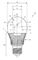
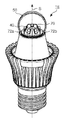
도 1은 본 발명에 따른 광원(10)의 측면 뷰를 도시한다. 광원(10)은 반투명 외부 엔벌로프(30) 내에 위치되는 광 방출기(20)를 포함한다. 광 방출기(20)는 발광 디바이스(40)에 의해 방출되는 광의 적어도 일부분을 확산시키기 위한 확산기(표시되지 않음)를 포함하는 반투명 내부 엔벌로프(50)에 의해 적어도 부분적으로 둘러싸이는 발광 디바이스(40)(도 4 참조)를 포함한다. 확산기는 내부 엔벌로프(50)의 벽에 통합될 수 있고, 내부 엔벌로프(50)의 내부 벽 또는 외부 벽에 한 층으로서 도포될 수 있다. 반투명 내부 엔벌로프(50)의 직경(di)은 반투명 외부 엔벌로프(30)의 직경(do)보다 더 작다. 반투명 외부 엔벌로프(30)는 일반적으로 반투명하지 않은 베이스(60)에 접속된다. 또한, 반투명 외부 엔벌로프(30)는 대칭축(S)을 포함한다. 또한, 도 1에서, 가상 베이스-면(P)은 대쉬-도트선(dash-dotted line)으로 표시된다. 이러한 가상 베이스-면(P)은 대칭축(S)에 실질적으로 직교하는 것으로 정의되고, 반투명 외부 엔벌로프(30)의 일부분인 접속점(C)과 교차한다. 접속점(C)은 반투명 외부 엔벌로프(30)의 중심(M)으로부터의 가장 먼 거리에 있는 베이스(60)와 반투명 외부 엔벌로프(30) 사이의 인터페이스에서 반투명 외부 엔벌로프(30)의 광 투과 부분이다. 단지 가장 먼 거리가 발견되어야 하는 방향을 정의하기 위해 사용됨에 따라, 반투명 외부 엔벌로프(30)의 중심(M)의 정확한 위치는 필요하지 않다.1 shows a side view of a
광 방출기(20)는 베이스(60)로부터 떨어진 가상 베이스-면(P)으로부터의 거리(D)에 반투명 외부 엔벌로프(30) 내에 위치된다.The
가상 베이스-면(P)은 외부 엔벌로프의 내부의 광 방출기에 의해 방출되는 광을 물리적으로 차단하는 테두리를 정의한다. 가상 면이 베이스와 가장 가까운 반투명 점으로서 정의되는 접속점(C)과 교차함에 따라, 접속점은 여전히 광을 방출하는 베이스에 가장 가까운 점이다. 가상 베이스-면(P)을 통해 베이스와 광 방출기 사이의 거리를 정의함에 따라, 도입부에 인용된 바와 같은 사전공개되지 않은된 특허출원에 나타나는 실시예들에 비해 방출 분포의 증가가 시작되는 점이 정의된다.The virtual base-plane P defines an edge that physically blocks the light emitted by the light emitters inside the outer envelope. As the imaginary plane intersects the connection point C, which is defined as the translucent point closest to the base, the connection point is still the point closest to the base emitting light. By defining the distance between the base and the light emitter through the virtual base-plane P, it is defined that the increase in emission distribution begins compared to the embodiments appearing in the non-published patent application as cited at the outset. do.
본 발명에 따른 광원(10)의 효과는 본 발명에 따른 광원(10)의 방출 프로파일(도 2 참조)이 증가한다는 점이다. 본 발명에 따른 광 방출기(20)가 확산기를 포함하는 반투명 내부 엔벌로프(50)를 포함하므로, 그리고 광 방출기(20)가 가상 베이스-면(P)으로부터의 거리 D에 위치되므로, 더 많은 광이 가상 베이스-면(P)을 향하는 방향으로 방출되고, 따라서, 가상 베이스-면(P)을 향하는 방향으로의 광원(10)의 방출 프로파일이 증가한다. 일반적으로, 확산기에서의 각각의 분산점은 충돌하는 광의 일부를 실질적으로 다수의 방향들로, 그리고 등방성 분산의 경우 심지어 모든 방향으로 분산되도록 한다. 베이스(60)로부터 이러한 분산 광 방출기(20)의 "상승(elevating)"은 광이 광원(10)으로부터 방출되는 각들을 증가시킬 것이고, 따라서, 방출 프로파일을 증가시킨다.The effect of the
광 방출기(20)와 가상 베이스-면(P) 사이의 거리(D)가 제로(0)인 경우, 광 방출기(20)의 어떠한 "상승"도 존재하지 않고, 베이스(60)의 테두리는 베이스로부터 외부 엔벌로프를 향해 지시하는 대칭축(S)을 따르는 방향으로부터 90도보다 더 큰 각으로 광의 상당 부분이 광원(10)에 의해 방출되는 것을 차단할 것이며, 이는 실질적으로 180도보다 더 크지 않은 광 분포에 대응한다. 이러한 실시예에서, 실질적으로 어떠한 광도 가상 베이스-면(P)을 향해 방출되지 않을 것이다. 가상 베이스-면(P)으로부터의 거리(D)에 광 방출기(20)를 위치시킴으로써, 내부 엔벌로프(50)의 확산기로부터 분산된 광은, 분산된 광의 더 큰 기여분이 가상 베이스-면(P)을 향해 방출될 것이며, 따라서, 180도를 초과하도록 방출 분포가 증가함을 보장할 것이다.If the distance D between the
본 발명에 따른 광원(10)의 추가적인 이점은 베이스(60)로부터 거리(D)에 있는 외부 엔벌로프(30) 내의 광 방출기(20)가 마치 광원(10)이 필라멘트를 포함하는 것처럼 - 동작 동안 - 광원(10)의 외형을 생성하기 위해 사용될 수 있다는 점이다. 백열 광원들에서, 필라멘트는 매우 높은 강도의 광을 방출한다. 인간의 눈이 이러한 높은 강도를 핸들링할 수 없음에 따라, 공지된 백열 광원들 내의 이러한 필라멘트는 유리 엔벌로프 내의 빛을 내는 구형으로서 인간 눈에 의해 종종 관측된다. 빛을 내는 구형이 백열 광원에서 인지되는 것과 실질적으로 동일한 위치에 내부 엔벌로프(20)를 적용함으로써, 동작 시, 본 발명에 따른 광원(10)에 의한 백열 광원의 외형은 매우 잘 모방될 수 있다. 이는 특히, 백열 광원 내의 필라멘트의 위치가 중요한 광학 설계들에서 유리할 수 있다. 본 발명에 따른 광원(10)은 특히 발광 다이오드들(40)(도 4 참조)이 발광 디바이스들로서 사용되는 경우, 백열 광원과 실질적으로 유사한 특성들을 가지는 동시에 훨씬 더 에너지 효율적인 대체 램프로서 직접 사용될 수 있다.A further advantage of the
베이스와 광 방출기(20) 사이의 거리(D)는 빔 폭이 적어도 220도 FWHM이도록 선택될 수 있다. 이는 통상적으로, 내부 엔벌로프(50)의 무게 중심이 광원(10)의 베이스(60)에 대해 외부 엔벌로프(30)의 높이의 1/4과 외부 엔벌로프(30)의 높이의 3/4 사이의, 바람직하게는 광원(10)의 베이스(60)에 대한 외부 엔벌로프(30)의 높이의 1/3과 외부 엔벌로프(30)의 높이의 2/3 사이의 위치에 위치지정되는 결과를 가져온다. 외부 엔벌로프(30)의 높이는 대칭축(S)의 방향으로 측정된다.The distance D between the base and the
컴포넌트들의 기하학적 구조(geometry)는 빔 폭이 적어도 220도 FWHM이도록 선택된다. 이는 내부 엔벌로프의 최대 직경에서의 내부 엔벌로프의 표면상의 점 및 접속점(C)에 접속하는 라인(미도시)과 대칭축(S) 사이의 각이 90도보다 작아야 하는, 바람직하게는 45도보다 작아야 하는, 바람직하게는 30도보다 작아야 하는, 컴포넌트들의 기하학적 구조를 선택함으로써 달성될 수 있다. 도 1에 도시된 실시예에서, 이전 라인에서 정의된 각은 대략 25도이며, 이러한 램프는 약 250도 FWHM의 빔 각을 초래한다. 또한, 내부 엔벌로프(20)의 확산도는 바람직하게는 높으며, 바람직하게는 80도보다 더 큰 FWHM이다.The geometry of the components is chosen such that the beam width is at least 220 degrees FWHM. This means that the angle between the line (not shown) connecting to the point on the surface of the inner envelope and the connection point C at the maximum diameter of the inner envelope and the axis of symmetry S should be less than 90 degrees, preferably more than 45 degrees. It can be achieved by selecting the geometry of the components, which should be small, preferably smaller than 30 degrees. In the embodiment shown in FIG. 1, the angle defined in the previous line is approximately 25 degrees, such a lamp resulting in a beam angle of about 250 degrees FWHM. In addition, the diffusivity of the
내부 엔벌로프(20)는 발광 디바이스(40)를 수용하기 위한 컷아웃 부분(55)을 포함한다. 도 1에 도시된 실시예에서, 컷 아웃 부분(55)은 구형 내부 엔벌로프(20)를 통하는 평면 컷으로서 형성된다. 물론, 다른 형상의 컷아웃 부분(55) 역시 가능할 수 있다. 내부 엔벌로프(20)의 직경(di)은 컷아웃 부분(55)의 직경(dc)보다 더 크다. 그 결과, 내부 엔벌로프(20)는 발광 디바이스(40)를 포함하는 회로 기판(70)(도 4b 참조)과 내부 엔벌로프(20) 사이의 교차점에서 바깥으로 튀어나오게 된다(bulge). 내부 엔벌로프(20)의 이러한 초기 확장은 내부 엔벌로프(20)에서의 확산기의 일부분이 실질적으로 가상 베이스-면(P)을 대향하도록 한다. 따라서, 더 많은 광이 가상 베이스-면(P)을 향해 분산될 것이며, 따라서 발광 디바이스(10)의 광의 더 많은 부분이 가상 베이스-면(P)을 향해 방출되는 것을 보장한다. 따라서, 광원(10)의 방출 분포가 더 증대될 수 있다.The
광원의 실시예들(10, 12)의 내부 엔벌로프(20)가 모두 구형 형상을 가지지만, 내부 엔벌로프(20)는 물론 임의의 형상을 가질 수 있다. 이러한 구형 형상의 이점은 상대적으로 높은 강도에서 빛을 내는 필라멘트가 또한 빛을 내는 구형 공으로서 인지된다는 점이며, 따라서, 이러한 구형 내부 엔벌로프(20)를 사용하는 것은 동작 시의 광원이 백열 광원들과 거의 유사하도록 할 수 있다.Although the
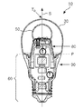
광 방출기(20)는 접속 수단(80)을 통해 외부 엔벌로프(30) 내에 위치된다. 접속 수단(80)은 물론 임의의 형상을 가질 수 있다. 그러나 접속 수단(80)은 바람직하게는 회로 기판(70)으로부터 확장하는 빈(hollow) 원뿔 형상을 가질 수 있으며, 상기 회로 기판 상에서 발광 디바이스(40)가 베이스를 향해 접속된다. 원뿔 형상 접속 수단(80)의 폭은 바람직하게는, 광 방출기(20)에 의해 방출되는 어떠한 광도 접속 수단(80)에 의해 차단되지 않도록, 베이스(60)의 직경보다 더 작다. 빈 원뿔 형상 접속 수단(80) 내에, 전력을 사용된 발광 디바이스(40)에 대해 적절한 레벨로 변환하기 위한 추가적인 전자 회로(electronics)가 위치될 수 있으며, 상기 추가적인 전자 기기는 발광 디바이스를 구동하기 위한 특정 전자 회로를 포함할 수 있다. 마지막으로, 접속 수단(80)은 열 전도 기능을 가질 수 있다. 발광 다이오드들(40)을 발광 디바이스들(40)로 사용하는 경우, 발광 디바이스(40)의 쿨링이 중요한 문제이다. 광 방출기(20) 내에, 광 방출기(20) 내의 발광 디바이스들(40)의 온도를 감소 및/또는 제한하기 위한 쿨링 수단이 있을 공간이 존재하지 않는다. 접속 수단(80)을 사용하는 경우, 접속 수단(80)은 발광 디바이스들(40)로부터의 열을, 예를 들어, 추가적인 열 전송 수단(90)이 존재할 수 있는 베이스(60)를 향해 전도하기 위해 사용될 수 있다.The
베이스(60)는 외부 엔벌로프(30)에 접속된다. 이러한 베이스(60)는 현재 실시예에서 발광 디바이스들(40)로부터 접속 수단(80)을 통해 주위(environment)로 열을 전도하는 쿨링 핀들(90)로 구성되는 열 전달 수단(90)을 포함한다. 전술된 바와 같이, 또한 다른 열 전달 수단(90), 예를 들어, 쿨링 액체와 같은 쿨링 유체와 열을 교환하는 열 교환기들(미도시)이 사용될 수 있다. 또한 도 1에 도시된 베이스(60)는 외부 전원(미도시)에 공지된 백열 광원들을 접속시키기 위해 사용되는 권선들과 유사한 권선을 포함한다. 따라서, 광원(10)은 이러한 유사한 권선을 가지는 공지된 백열 광원들에 대한 대체물로서 직접 사용될 수 있다. 물론, 광원(10)을 일부 외부 전원에 접속시키기 위한 다른 수단이 또한 사용될 수 있다.The
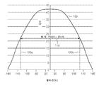
도 2는 도 1에 도시된 발명에 따른 광원(10)의 방출 분포를 표시하는 그래프를 도시한다. 도 2에 도시된 그래프에서, 광의 강도는 그래프의 수직축을 따라 그려지고 방위각은 수평축을 따라 그려진다. 빔의 폭은 광 강도 곡선(100)의 중심에 양방향 화살표(110)로 표시되는 바와 같이 최대 강도의 절반에서 정의된다. 양방향 화살표(110)와 광 강도 곡선(100) 사이의 교차점으로부터 시작하는 점선들(120a, 120b)은 반값 전폭에서 광원(10)의 각 분포를 정의한다. 현재 예에서, 광원(10)의 방출 분포의 폭은 16.5 밀리미터인 광 방출기(20)와 베이스(60) 사이의 거리(D)(도 1 참조)를 가지는 광원(10)에 대해 254도 FWHM이다. 이는 외부 엔벌로프(30)의 높이의 1/2의 내부 엔벌로프(50)의 무게 중심의 위치와 등가이다.FIG. 2 shows a graph showing the emission distribution of the
도 3a 및 3b는 본 발명에 따른 광원(10, 12)의 상이한 실시예들의 측면 뷰들을 도시한다. 도 3a 및 3b에 도시된 상이한 실시예들에서, 외부 엔벌로프(30, 32)는 추가 확산기를 포함한다. 추가 확산기는 외부 엔벌로프(30, 32)에 의해 투과되는 광의 일부분을 재방향설정(redirecting)하도록 구성된다. 확산기는 본 발명에 따라 광원(10, 12)의 외형에 충돌하는 미리 정의된 확산도를 포함한다. 확산도는 투과된 빔의 파라미터 반값 전폭(FWHM)을 사용하여 콜리메이트 펜슬 빔의 동작을 분산시킴으로써 정의된다. 콜리메이트 펜슬 빔은 1도 미만의 콜리메이트 빔의 FWHM를 포함한다. FWHM은 5도와 120도 사이일 수 있다. 바람직하게는, 확산도는 일부 추가적인 재방향설정을 가지기 위해, 필라멘트 효과를 가지기 위해, 그리고 또한 높은 효율성을 가지기 위해 5도와 40도 사이이다. 도 3a에서, 확산도는 가장 높은데 이는 내부 엔벌로프(50)의 상세 항목들이 거의 가시적이지 않은 결과를 초래한다. 내부 엔벌로프(50)가 통상적으로 청색광을 황색 광으로 변환하는 발광 물질을 포함함에 따라, 내부 엔벌로프(50)는 통상적으로, 광원(10, 12)이 스위치 오프되는 경우, 황색 재현을 가진다. 이는 바람직하지 않다. 상대적으로 높은 확산도(30도와 120도 사이의 FWHM)를 가지는 추가 확산기를 선택함으로써, 내부 엔벌로프(50)의 상세 항목들은 덜 가시적이게 되며, 이는 내부 엔벌로프(50)의 황색 재현을 포함한다. 도 3b에서, 추가적인 확산기는 더 낮은 확산도(5도와 30도 사이의 FWHM)를 가진다. 그 결과, 내부 엔벌로프 내의 상세 항목들은 상대적으로 양호하게 가시적이며, 효율성이 더 높다. 광원(10)으로부터 방출되는 광의 빔 각은 도 3a에서와 같이 더 높은 확산도의 경우보다 더 작을 것이지만, 종래 기술의 광원들에서보다는 더 크다.3A and 3B show side views of different embodiments of
본 발명에 따른 광원(10, 12)에서의 내부 엔벌로프(50)의 이러한 황색 재현을 더 감소시키기 위해, 외부 엔벌로프(30, 32)에 대향하는 내부 엔벌로프(50)의 벽인 내부 엔벌로프(50)의 외부 벽은 백색 확산층을 포함할 수 있다. 이러한 백색 확산층은 광원(10, 12)에 의해 방출되는 광의 색에 단지 아주 조금 영향을 준다. 광원(10, 12)이 오프 상태인 경우 내부 엔벌로프(50)의 외형은 명백하게 변경될 수 있다.In order to further reduce this yellow representation of the
도 4a 및 4b는 본 발명에 따른 광원(10)의 상이한 상세 레벨들에서의 횡단면 뷰들을 도시한다. 도 4a는 전체 광원(10)의 횡단면 뷰를 도시하고, 도 4b는 발광 다이오드 디바이스들(40)인 발광 디바이스들(40)을 포함하는 내부 엔벌로프(50)의 상세한 횡단면 뷰를 도시한다. 또한, 외부 엔벌로프(30)와 대칭축(S) 사이의 교차점(T0)은 도 4a에서 표시되는 외부 엔벌로프(30)의 최상부(T0)로서 표시된다. 또한, 내부 엔벌로프(50)와 대칭축(S) 사이의 교차점(Ti)은 도 4b에 표시된 내부 엔벌로프(50)의 최상부(Ti)로서 표시된다.4A and 4B show cross-sectional views at different levels of detail of the
도 4a에서, 접속 엘리먼트(80)는 광 방출기(20)로부터 베이스(60)를 향해 넓어지는 원뿔 형상의 접속 엘리먼트(80)라는 점이 명백히 보여질 수 있다. 또한, 원뿔 형상의 접속 엘리먼트(80)는 비었으며, 예를 들어, 전력을 사용된 발광 디바이스(40)에 대한 적합한 레벨로 변환하기 위한 추가적인 전자 회로를 위한 공간을 제공할 수 있다. 또한, 접속 수단(80)은 발광 디바이스들(40)로부터의 열을 예를 들어, 쿨링 핀들(90)과 같은 추가적인 열 전달 수단(90)이 존재할 수 있는 베이스(60)를 향해 전송하기 위한 열-전도 기능을 가질 수 있다.In FIG. 4A, it can be clearly seen that the connecting
회로 기판(70)은 바람직하게는, 비교적 저렴하게 생산될 수 있으므로, 도 4b에 도시된 바와 같이 평면 회로 기판(70)일 수 있다. 그러나 회로 기판(70)은 또한, 대칭축(S)에 대해, 그리고/또는 서로에 대해 상이한 각들로 배열되는 몇몇 회로 기판들(미도시)로 구성될 수 있다. 또한, 도 4b로부터 보여질 수 있는 바와 같이, 회로 기판(70)은 하나의 발광 다이오드(40)를 포함할 수 있지만, 또한 둘 이상의 발광 다이오드(40)를 포함할 수도 있다. 회로 기판(70)은 내부 엔벌로프(50)에 대향하는 회로 기판(70)의 측면 상에 반사 및/또는 발광 층을 더 포함할 수 있다. 이러한 실시예에서, 반사층은, 예를 들어, 광의 재사용을 가능하게 하기 위해 사용될 수 있고, 발광 물질은 광원(10)에 의해 방출되는 색을 미세-조정하기 위해 사용될 수 있고 그리고/또는 회로 기판(70)에 적용되는 발광 다이오드(40)의 방출 특성을 보정하기 위해 사용될 수 있다. 발광 디바이스들(40)은, 예를 들어, 청색 광을 방출할 수 있거나, 또는 임의의 다른 색의 광을 방출할 수 있으며, 예를 들어, 인광체-변환 발광 다이오드들(40)과 같은, 인광체-변환 광원들(40)을 포함할 수 있다.The
내부 엔벌로프(50)는, 예를 들어, 몰딩 이전에 폴리카보네이트에서 혼합된 발광 물질을 포함하는 폴리카보네이트와 같은 투명 폴리머의 사출 성형(injection molding)을 통해 제조될 수 있다. 또한, 발광 물질은 폴리카보네이트가 내부 엔벌로프(50)의 내부 및/또는 외부 표면 상의 층으로서 몰딩된 후 도포될 수 있다. 선택적으로, TiO2, SiO2 또는 Al2O3와 같은 추가적인 확산 물질은 폴리카보네이트 내부에 그리고/또는 폴리카보네이트의 최상부의 층으로서 도포될 수 있다. 대안적으로, 내부 엔벌로프(50)는, 예를 들어, 발광 물질 및 선택적으로 추가적인 확산 물질이 적절한(폴리머) 매트릭스로 존재할 수 있는 유리 또는 플라스틱 투명 또는 반투명 오목한 기판의 플러시 코팅 또는 스프레이 코팅으로 만들어질 수 있다.The
대안적으로, 내부 엔벌로프(50)는, 예를 들어, 설정 이전에 실리콘 고무에서 혼합된 발광 물질을 실리콘 고무와 같은 투명 폴리머의 사출 성형을 통해 제조될 수 있다. 선택적으로, TiO2, SiO2 또는 Al2O3와 같은 추가적인 확산 물질은 실리콘 고무 내에 도포될 수 있다.Alternatively, the
도 5a 및 5b는 외부 엔벌로프(30)가 생략된 본 발명에 따른 상이한 광원들(14, 16)에서의 횡단면 뷰들을 도시한다. 외부 엔벌로프(30)는 도 5a에서의 내부 엔벌로프(52)의 형상을 더욱 명확하게 도시하기 위해, 그리고 도 5b에서의 발광 디바이스들(40)의 특정 배열을 더욱 명확하게 도시하기 위해 도 5a 및 5b에는 표시되지 않는다. 그러나 동작시, 외부 엔벌로프(30)는 도 1에 표시된 바와 같이, 그리고 청구 범위에 나타난 바와 같이 존재한다. 도 5a에 도시된 실시예에서, 세장된(elongated) 내부 엔벌로프(52)는 대칭축(S)을 따른 내부 엔벌로프(52)의 디멘젼이 대칭축(S)에 직교하는 방향으로의 내부 엔벌로프(52)의 디멘젼보다 더 큰 것으로 도시된다. 이러한 내부 엔벌로프(52)는 내부 엔벌로프(50)가 실질적으로 구형 형상을 포함하는 이전 실시예들에 비해 상이한 필라멘트 효과가 있다. 도 5b에 도시된 실시예에서, 발광 디바이스(40)는 대칭축(S)에 대해 그리고 서로에 대해 상이한 각들로 배열되는 상이한 회로 기판들(70, 72a, 72b) 상에 배열되는 복수의 발광 다이오드들(40)로 구성된다. 이러한 배열은, 베이스-면(P)(도 5b에는 미도시)을 향해 더 많은 광이 방출됨에 따라, 광원(16)의 더 증가한 공간 방출 분포를 생성한다. 실질적으로 균일한(homogeneous) 색 분포를 획득하기 위해, 복수의 발광 다이오드들은 바람직하게는 실질적으로 동일한 색의 광을 방출한다.5a and 5b show cross-sectional views in different
외부 엔벌로프(30)는 예를 들어, 투명 유리로 만들어질 수 있다. 적절한 분산도는 예를 들어, 내부 및/또는 외부 표면의 샌드 블라스팅(sand blasting) 또는 에칭에 의해, 또는, 예를 들어, 적절한(폴리머) 매트릭스에서 TiO2, SiO2 또는 Al2O3와 같은 적절한 확산 물질로 플러시 코팅 또는 스프레이 코팅함으로써 달성될 수 있다. 코팅 공정 후, 매트릭스 물질은 가열에 의해 제거될 수 있다. 대안적으로, 외부 엔벌로프(30)는 추가적인 확산 물질을 포함하는 실리콘 고무 또는 폴리카보네이트와 같은 반투명 플라스틱으로 만들어질 수 있다. 외부 엔벌로프(30)는, 사용되는 물질들의 특징들에 따라, 예를 들어, 사출 중공 성형, 사출 성형 또는 압축 성형에 의해 제조될 수 있다.The
본 발명에 따른 일 실시예에서, 레드-오렌지 질화물 인광체가 내부 엔벌로프(50)(즉, 원격 발광 엘리먼트)에 도포될 수 있는 반면, 회로 기판(70) 상에는 적어도 청색을 방출하는 발광 다이오드(40)가 적용되고, 황록색 인광체가 내부 엔벌로프(50)로부터 방출되는 백색계열(whitish) 광을 제공하기 위해 도포된다.In one embodiment according to the invention, a red-orange nitride phosphor may be applied to the inner envelope 50 (ie, a remote light emitting element), while the
추가적인 실시예에서, 황록색 인광체, 예를 들어, 황록색 가넷 인광체가 내부 엔벌로프(50)에 도포되고, 레드-오렌지 인광체, 예를 들어, 레드-오렌지 질화물 인광체가 회로 기판(70) 상에 또는 청색 광을 방출하는 발광 다이오드(40)에 근접하여 발광 다이오드(40) 상에 도포된다.In a further embodiment, a yellow green phosphor, eg, a yellow green garnet phosphor, is applied to the
추가적인 실시예는 내부 엔벌로프(50)에 적용되는 레드-오렌지 및 황록색 인광체의 혼합물을 포함하는 반면, 회로 기판(70)상에 적어도 청색 광을 방출하는 발광 다이오드(40)가 제공된다.Further embodiments include a mixture of red-orange and yellow-green phosphors applied to the
대안적으로, 일 실시예에서, 레드-오렌지 인광체, 예를 들어, 레드-오렌지 질화물 인광체가 내부 엔벌로프(50)에 도포되고, 황록색 인광체, 예를 들어, 황록색 가넷 인광체가 외부 엔벌로프(30)에 도포되는 반면, 회로 기판(70)은 적어도 청색 광을 방출하는 발광 다이오드(40)를 포함한다.Alternatively, in one embodiment, a red-orange phosphor, eg, a red-orange nitride phosphor, is applied to the
추가적인 실시예에서, 청색 광을 방출하는 발광 다이오드(40) 및 적색 광을 방출하는 발광 다이오드(40)는 둘 다 회로 기판(70)상에 장착되는 반면, 내부 엔벌로프(50)는 적어도 황록색 인광체를 포함한다.In a further embodiment, both the
추가적인 실시예에서, 청색 광으로 조사시 레드-오렌지 광을 방출하는 발광 물질을 포함하는 청색 광 및 적색광을 방출하는 발광 다이오드(40)가 회로 기판(70) 상에 장착되는 반면, 내부 엔벌로프(50)는 적어도 황록색 가넷 인광체를 포함한다.In a further embodiment, a blue and red
추가적인 실시예에서, 백색광을 방출하는 발광 다이오드(40)가 회로 기판(70) 상에 장착되는 반면, 내부 엔벌로프(50)는 확산 물질을 포함한다. 이러한 실시예는 내부 엔벌로프(50) 또는 외부 엔벌로프(30)에 도포되는 발광 물질들을 포함하지 않지만, 여전히 필라멘트가 존재한다.In a further embodiment, a
모든 구성들에서, 적색 발광 디바이스(40) 또는 적색 발광 물질은 적어도 600 nm, 바람직하게는 적어도 610 nm의 피크 파장을 가지며, 660 nm, 바람직하게는 650 nm, 가장 바람직하게는 640 nm의 최대 피크 파장을 가진다.In all configurations, the red
가넷 인광체는 통상적으로 일반적인 화학식을 포함한다:Garnet phosphors typically include the general formula:
![]()
![]()
그리고 가넷 인광체는 통상적으로 일반적인 화학식을 포함한다:And garnet phosphors typically include the general formula:
![]()
![]()
전술된 실시예들이 본 발명을 제한하도록 예시한다기보다는, 당업자가 첨부된 청구항들의 범위에서 벗어나지 않고 많은 대안적인 실시예들을 설계할 수 있을 것이라는 점에 유의해야 한다.Rather than exemplify the foregoing embodiments as limiting the invention, it should be noted that those skilled in the art will be able to design many alternative embodiments without departing from the scope of the appended claims.
청구범위에서, 괄호 사이에 위치한 임의의 참조 부호는 본 발명을 제한하는 것으로 해석되지 않을 것이다. 용어 "포함하다" 및 그 활용어들의 사용은 청구 범위에 언급된 것들이 아닌 엘리먼트들 또는 단계들의 존재를 배제하지 않는다. 단수인 엘리먼트(엘리먼트에 선행하는 부정관사 "a" 또는 "an")는 복수의 이러한 엘리먼트들의 존재를 배제하지 않는다. 본 발명은 몇몇 다른 엘리먼트들을 포함하는 하드웨어에 의해 구현될 수 있다. 몇몇 수단을 열거하는 디바이스 청구항에서, 이들 수단들 중 몇몇은 하나의 하드웨어 또는 하드웨어의 동일한 항목에 의해 구현될 수 있다. 특정 수단들이 서로 다른 종속 청구항에서 인용된다는 단순한 사실은 이들 수단들의 조합이 유리하게 사용될 수 없다는 것을 나타내지는 않는다.In the claims, any reference signs placed between parentheses shall not be construed as limiting the invention. The use of the term "comprises" and their terms does not exclude the presence of elements or steps other than those mentioned in a claim. A singular element (the indefinite article “a” or “an” preceding an element) does not exclude the presence of a plurality of such elements. The present invention can be implemented by hardware including some other elements. In the device claim enumerating several means, some of these means may be embodied by one piece of hardware or the same item of hardware. The simple fact that certain means are cited in different dependent claims does not indicate that a combination of these means cannot be used advantageously.
Claims (21)
상기 광 방출기(20)는 발광 디바이스(40)를 포함하고 상기 발광 디바이스(40)를 적어도 부분적으로 둘러싸는 반투명 내부 엔벌로프(50, 52)를 포함하고, 상기 반투명 내부 엔벌로프(50, 52)는 상기 발광 디바이스(40)에 의해 방출되는 광의 적어도 일부분을 확산시키기 위한 확산기를 포함하며, 상기 반투명 내부 엔벌로프(50, 52)의 직경(di)은 반투명 외부 엔벌로프(30, 32)의 직경(do)보다 더 작고,
상기 반투명 외부 엔벌로프(30, 32)는 베이스(60)에 접속되며, 대칭축(S)을 더 포함하고, 가상 베이스-면(P)은 상기 대칭축(S)에 실질적으로 직교하는 것으로 정의되며 상기 반투명 외부 엔벌로프(30, 32)의 일부분인 접속점(C)과 교차하고, 상기 접속점(C)은 상기 반투명 외부 엔벌로프(30, 32)와 상기 반투명 외부 엔벌로프(30, 32)의 중심(M)으로부터 가장 먼 거리에 있는 베이스(60) 사이의 인터페이스에서 상기 반투명 외부 엔벌로프(30, 32)의 광 투과 부분이며,
상기 광 방출기(20)는 상기 베이스(60)로부터 떨어진 상기 가상 베이스-면(P)으로부터의 거리(D)에서 상기 반투명 외부 엔벌로프(30, 32) 내에 배열되는 광원.As a light source 10, 12, 14, 16 comprising a light emitter 20 arranged in a translucent outer envelope 30, 32,
The light emitter 20 includes a translucent inner envelope 50, 52 that includes a light emitting device 40 and at least partially surrounds the light emitting device 40, and the translucent inner envelope 50, 52. Includes a diffuser for diffusing at least a portion of the light emitted by the light emitting device 40, wherein the diameter d i of the translucent inner envelope 50, 52 is of the translucent outer envelope 30, 32; Smaller than the diameter (d o ),
The translucent outer envelope 30, 32 is connected to the base 60 and further comprises an axis of symmetry S, the virtual base-plane P being defined as being substantially orthogonal to the axis of symmetry S and said Intersects the junction C which is part of the translucent outer envelope 30, 32, the junction C being the center of the translucent outer envelope 30, 32 and the translucent outer envelope 30, 32. The light transmissive portion of the translucent outer envelopes 30, 32 at the interface between the bases 60 at the furthest distance from M),
The light emitter (20) is arranged in the translucent outer envelope (30, 32) at a distance (D) from the virtual base-plane (P) away from the base (60).
상기 확산기는 발광 물질을 포함하고, 그리고/또는 상기 확산기는 발광 디바이스(40)에 의해 방출되는 광을 더욱 긴 파장의 광으로 변환하도록 구성되는 발광 물질로 이루어지는 광원.The method of claim 1,
The light diffuser comprises a light emitting material, and / or the light diffuser is configured of a light emitting material configured to convert light emitted by the light emitting device (40) into light of a longer wavelength.
상기 발광 디바이스(40)는 발광 다이오드(40) 및/또는 발광 레이저 다이오드인 광원.The method according to claim 1 or 2,
The light emitting device (40) is a light emitting diode (40) and / or a light emitting laser diode.
상기 발광 디바이스(40)는 상기 가상 베이스-면(P)에 실질적으로 평행하게 배열된 실질적으로 평면 회로 기판(70) 상에 배열되고, 또는 상기 광원(10, 12, 14, 16)은 상기 대칭축(S)에 대해 그리고/또는 서로에 대해 상이한 각들로 배열되는 복수의 회로 기판들(72a, 72b) 상에 배열되는 복수의 발광 디바이스들(40)을 포함하는 광원.4. The method according to any one of claims 1 to 3,
The light emitting device 40 is arranged on a substantially planar circuit board 70 arranged substantially parallel to the virtual base-plane P, or the light sources 10, 12, 14, 16 are arranged on the axis of symmetry. A light source comprising a plurality of light emitting devices (40) arranged on a plurality of circuit boards (72a, 72b) arranged at different angles with respect to (S) and / or with respect to each other.
상기 내부 엔벌로프(50, 52)의 최상부(Ti)로부터 떨어져 있는 부분들에서 상기 내부 엔벌로프(50, 52)에 대한 방사의 상대적 레벨을 높이기 위해 대칭축(S)을 통한 단면 뷰에서 보여질 때, 상기 발광 디바이스(40)로부터 배트윙(batwing) 또는 나비 형상 방사 프로파일을 생성하기 위해 상기 내부 엔벌로프(50, 52) 내에 배열되며, 상기 내부 엔벌로프(50, 52)의 최상부(Ti)는 상기 대칭축(S)과 교차하는 상기 내부 엔벌로프(50, 52)의 일부분인 광원.4. The method according to any one of claims 1 to 3,
To be seen in the cross-sectional view through the axis of symmetry S to increase the relative level of radiation with respect to the inner envelope 50, 52 at portions away from the top T i of the inner envelope 50, 52. When arranged within the inner envelope 50, 52 to produce a batwing or butterfly shaped radiation profile from the light emitting device 40, the top T i of the inner envelope 50, 52. Is a portion of the inner envelope (50, 52) that intersects the axis of symmetry (S).
상기 내부 엔벌로프(50, 52)의 직경(di)은 상기 외부 엔벌로프(30, 32)의 직경(do)의 70% 이하이고, 그리고/또는 상기 내부 엔벌로프(50, 52)의 직경(di)은 상기 외부 엔벌로프(30, 32)의 직경(do)의 50% 이하이고, 그리고/또는 상기 내부 엔벌로프(50, 52)의 직경(di)은 상기 외부 엔벌로프(30, 32)의 직경(do)의 40% 이하인 광원.4. The method according to any one of claims 1 to 3,
The diameter d i of the inner envelope 50, 52 is less than or equal to 70% of the diameter d o of the outer envelope 30, 32 and / or of the inner envelope 50, 52. The diameter d i is 50% or less of the diameter d o of the outer envelope 30, 32, and / or the diameter d i of the inner envelope 50, 52 is the outer envelope. A light source that is 40% or less of the diameter d o of (30, 32).
상기 내부 엔벌로프(50, 52)는 상기 발광 디바이스(40)를 수용하기 위한 컷아웃(cut-out) 부분(55)을 포함하고, 상기 내부 엔벌로프(50, 52)의 직경(di)은 상기 컷아웃 부분(55)의 직경(dc)보다 더 크고, 상기 내부 엔벌로프(50, 52)의 직경(di)은 상기 컷아웃 부분(55)의 직경(dc)을 측정하기 위한 방향과 평행한 방향으로 측정되는 광원.4. The method according to any one of claims 1 to 3,
The inner envelope 50, 52 includes a cut-out portion 55 for receiving the light emitting device 40, the diameter d i of the inner envelope 50, 52. Is larger than the diameter d c of the cutout portion 55, and the diameter d i of the inner envelope 50, 52 measures the diameter d c of the cutout portion 55. A light source measured in a direction parallel to the direction for.
상기 내부 엔벌로프(50, 52)는 완전한 구형 형상 또는 부분적 구형 형상을 포함하는 광원.4. The method according to any one of claims 1 to 3,
The inner envelope (50, 52) comprises a complete spherical shape or a partial spherical shape.
상기 내부 엔벌로프는 상기 대칭축(S)에 직교하는 방향으로의 디멘젼에 비해 상기 대칭축(S)에 평행한 방향으로 더 큰 디멘젼을 가지는 광원.4. The method according to any one of claims 1 to 3,
And the inner envelope has a larger dimension in a direction parallel to the axis of symmetry (S) than a dimension in the direction orthogonal to the axis of symmetry (S).
상기 내부 엔벌로프(50, 52) 및/또는 상기 외부 엔벌로프(30, 32)는 적어도 부분적으로 반사적인 층을 포함하는 광원.4. The method according to any one of claims 1 to 3,
Wherein the inner envelope (50, 52) and / or the outer envelope (30, 32) comprise at least partially reflective layers.
상기 적어도 부분적으로 반사적인 층은 상기 내부 엔벌로프(50, 52)의 일부분 상에 그리고/또는 상기 외부 엔벌로프(30, 32)의 일부분 상에 배열되는 광원.The method of claim 10,
The at least partially reflective layer is arranged on a portion of the inner envelope (50, 52) and / or on a portion of the outer envelope (30, 32).
상기 광 방출기(20)는 상기 광 방출기(20)를 상기 베이스(60)에 접속시키고 상기 광 방출기(20)와 상기 가상 베이스-면(P) 사이의 거리(D)를 정의하기 위한 접속 엘리먼트(80) 상에 배열되는 광원.4. The method according to any one of claims 1 to 3,
The light emitter 20 connects the light emitter 20 to the base 60 and defines a distance D between the light emitter 20 and the virtual base-plane P. Light source arranged on 80).
상기 광 방출기(20)와 상기 가상 베이스-면(P) 사이의 거리(D)는 적어도 220도 반값 전폭 및/또는 적어도 250도 반값 전폭의 분포 면에서의 방출 분포를 생성하도록 선택되며, 상기 분포 면은 상기 대칭축(S)과 교차하는 가상 면인 광원.The method of claim 12,
The distance D between the light emitter 20 and the virtual base-plane P is selected to produce an emission distribution in a distribution plane of at least 220 degrees half-width full width and / or at least 250 degrees half-width full width. A light source is a virtual plane intersecting the plane of symmetry (S).
상기 접속 엘리먼트(80)는 상기 접속점(C)으로 상기 광 방출기(20)에 의해 방출되는 광이 상기 접속 엘리먼트(80)에 의해 방해받는 것을 방지하기 위해 상기 광 방출기(20)로부터 베이스(60)를 향해 넓어지는 원뿔-형상 접속 엘리먼트(80)인 광원.The method according to claim 12 or 13,
The connecting element 80 is connected from the light emitter 20 to the base 60 to prevent the light emitted by the light emitter 20 to the connecting point C from being disturbed by the connecting element 80. A light source, which is a cone-shaped connecting element 80 that widens toward.
상기 접속 엘리먼트(80)는 상기 발광 디바이스(40)로부터의 열을 추출하기 위해 상기 발광 디바이스(40)에 열적으로 접속되는 광원.The method according to any one of claims 12 to 14,
The connection element (80) is thermally connected to the light emitting device (40) for extracting heat from the light emitting device (40).
상기 베이스(60)는 상기 접속 엘리먼트(80)에 열적으로 접속되는 열 전달 수단(90)을 더 포함하는 광원.16. The method of claim 15,
The base (60) further comprises heat transfer means (90) thermally connected to the connection element (80).
상기 열 전달 수단(90)은 광이 쿨링 핀들(90) 사이의 갭들을 통해 상기 외부 엔벌로프(30, 32)로부터 방출되도록 하기 위한 대칭 축(S)에 평행한 방향으로 연장하는 쿨링 핀들(90)을 포함하는 광원.The method of claim 16,
The heat transfer means 90 extends cooling fins 90 extending in a direction parallel to the axis of symmetry S for allowing light to be emitted from the outer envelope 30, 32 through the gaps between the cooling fins 90. Light source).
상기 외부 엔벌로프(30, 32)는 상기 외부 엔벌로프(30, 32)를 통해 전송되는 광을 확산시키기 위한 추가 확산기를 포함하는 광원.4. The method according to any one of claims 1 to 3,
The external envelope (30, 32) includes a light diffuser for diffusing light transmitted through the external envelope (30, 32).
상기 추가 확산기는 5도 내지 120도의 반값 전폭의 확산도를 포함하고, 상기 확산도는 상기 확산기에 충돌하는 콜리메이트 펜슬 빔의 분산 거동에 의해 정의되며, 상기 충돌하는 콜리메이트 펜슬 빔의 공간적 분산을 초래하는 광원.The method of claim 18,
The further diffuser comprises a diffusivity of half full width from 5 degrees to 120 degrees, wherein the diffusivity is defined by the dispersion behavior of the collimated pencil beam impinging the diffuser, resulting in spatial dispersion of the collimating collimated pencil beam. Light source.
상기 외부 엔벌로프(30, 32)에 대향하는 상기 내부 엔벌로프(50, 52)의 벽은 확산층을 포함하는 광원.The method according to any one of claims 1 to 19,
A wall of the inner envelope (50, 52) opposite the outer envelope (30, 32) comprises a diffusion layer.
상기 광원(10, 12, 14, 16)은 상기 발광 디바이스(40)를 포함하는 표면(70, 72a, 72b)을 더 포함하고, 상기 표면(70, 72a, 72b)은 반사층을 포함하고 그리고/또는 발광 물질을 더 포함하고, 그리고/또는
상기 광원(10, 12, 14, 16)은 반사층 및/또는 상기 외부 엔벌로프(30, 32) 내의 반투명하지 않은 표면들에 도포되는 추가적인 발광 물질을 더 포함하고, 그리고/또는
상기 발광 디바이스(40)는 상기 대칭축(S)에 대해 그리고/또는 서로에 대해 상이한 각들에서 배열되는 복수의 발광 다이오드들(40)을 포함하고, 그리고/또는
상기 발광 디바이스(40)는 인광체-증가 발광 디바이스(40)를 포함하고, 그리고/또는
상기 발광 디바이스(40)는 청색 광을 방출하도록 구성되고, 상기 내부 엔벌로프(50, 52)는 상기 청색 광을 흡수하고, 상기 흡수된 광의 일부분을 황색 광으로 변환하기 위한 발광 물질을 포함하고, 그리고/또는
상기 발광 디바이스(40)는 상기 청색 광 및 레드-오렌지색 광을 방출하도록 구성되고, 그리고 상기 내부 엔벌로프(50, 52)는 상기 청색 광을 흡수하고, 상기 흡수된 광의 일부분을 황록색 광으로 변환하도록 구성되는 발광 물질을 포함하고, 그리고/또는
상기 내부 엔벌로프(50, 52)에 대향하는 상기 외부 엔벌로프(30, 32)의 벽은 상기 광 방출기(20)에 의해 방출되는 광을 더 긴 파장의 광으로 변환하기 위한 추가적인 발광층을 포함하고, 그리고/또는
상기 내부 엔벌로프(50, 52)에 대향하는 상기 외부 엔벌로프(30, 32)의 벽은 상기 광 방출기(20)에 의해 방출되는 광을 더 긴 파장의 광으로 변환하기 위한 유기 발광단 층을 포함하는 광원.4. The method according to any one of claims 1 to 3,
The light sources 10, 12, 14, 16 further comprise surfaces 70, 72a, 72b comprising the light emitting device 40, the surfaces 70, 72a, 72b comprising a reflective layer and / or Or further comprising a luminescent material, and / or
The light source 10, 12, 14, 16 further comprises a reflective layer and / or an additional luminescent material applied to non-translucent surfaces within the outer envelope 30, 32, and / or
The light emitting device 40 comprises a plurality of light emitting diodes 40 arranged at different angles with respect to the axis of symmetry S and / or with respect to each other, and / or
The light emitting device 40 comprises a phosphor-increasing light emitting device 40, and / or
The light emitting device 40 is configured to emit blue light, the inner envelope 50, 52 includes a light emitting material for absorbing the blue light and converting a portion of the absorbed light into yellow light, And / or
The light emitting device 40 is configured to emit the blue light and the red-orange light, and the inner envelope 50, 52 absorbs the blue light and converts a portion of the absorbed light into yellow green light. And / or comprise a luminescent material that is constructed
The walls of the outer envelopes 30, 32 opposite the inner envelopes 50, 52 include additional light emitting layers for converting light emitted by the light emitter 20 into light of longer wavelengths. , And / or
The walls of the outer envelope 30, 32 opposite the inner envelope 50, 52 form an organic luminophore layer for converting light emitted by the light emitter 20 into light of longer wavelengths. Including light source.
Applications Claiming Priority (2)
| Application Number | Priority Date | Filing Date | Title |
|---|---|---|---|
| CN200910139350.5 | 2009-05-04 | ||
| CN200910139350 | 2009-05-04 |
Publications (1)
| Publication Number | Publication Date |
|---|---|
| KR20120030404A true KR20120030404A (en) | 2012-03-28 |
Family
ID=42357831
Family Applications (1)
| Application Number | Title | Priority Date | Filing Date |
|---|---|---|---|
| KR1020117028885A KR20120030404A (en) | 2009-05-04 | 2010-04-23 | Light source comprising a light emitter arranged inside a translucent outer envelope |
Country Status (9)
| Country | Link |
|---|---|
| US (1) | US9175817B2 (en) |
| EP (1) | EP2427688B1 (en) |
| JP (2) | JP5711217B2 (en) |
| KR (1) | KR20120030404A (en) |
| CN (2) | CN102439351A (en) |
| BR (1) | BRPI1007605A2 (en) |
| CA (1) | CA2760767C (en) |
| RU (1) | RU2538098C2 (en) |
| WO (1) | WO2010128419A1 (en) |
Families Citing this family (72)
| Publication number | Priority date | Publication date | Assignee | Title |
|---|---|---|---|---|
| US10340424B2 (en) | 2002-08-30 | 2019-07-02 | GE Lighting Solutions, LLC | Light emitting diode component |
| US9412926B2 (en) * | 2005-06-10 | 2016-08-09 | Cree, Inc. | High power solid-state lamp |
| US8593040B2 (en) | 2009-10-02 | 2013-11-26 | Ge Lighting Solutions Llc | LED lamp with surface area enhancing fins |
| CN101718400A (en) * | 2009-12-11 | 2010-06-02 | 深圳市众明半导体照明有限公司 | Large-angle LED illuminating device |
| US8466611B2 (en) | 2009-12-14 | 2013-06-18 | Cree, Inc. | Lighting device with shaped remote phosphor |
| US8541933B2 (en) * | 2010-01-12 | 2013-09-24 | GE Lighting Solutions, LLC | Transparent thermally conductive polymer composites for light source thermal management |
| US9052067B2 (en) | 2010-12-22 | 2015-06-09 | Cree, Inc. | LED lamp with high color rendering index |
| US9310030B2 (en) | 2010-03-03 | 2016-04-12 | Cree, Inc. | Non-uniform diffuser to scatter light into uniform emission pattern |
| US9500325B2 (en) | 2010-03-03 | 2016-11-22 | Cree, Inc. | LED lamp incorporating remote phosphor with heat dissipation features |
| US8931933B2 (en) * | 2010-03-03 | 2015-01-13 | Cree, Inc. | LED lamp with active cooling element |
| US10359151B2 (en) | 2010-03-03 | 2019-07-23 | Ideal Industries Lighting Llc | Solid state lamp with thermal spreading elements and light directing optics |
| US9316361B2 (en) | 2010-03-03 | 2016-04-19 | Cree, Inc. | LED lamp with remote phosphor and diffuser configuration |
| US8882284B2 (en) | 2010-03-03 | 2014-11-11 | Cree, Inc. | LED lamp or bulb with remote phosphor and diffuser configuration with enhanced scattering properties |
| US9057511B2 (en) | 2010-03-03 | 2015-06-16 | Cree, Inc. | High efficiency solid state lamp and bulb |
| US20110227102A1 (en) * | 2010-03-03 | 2011-09-22 | Cree, Inc. | High efficacy led lamp with remote phosphor and diffuser configuration |
| US9062830B2 (en) * | 2010-03-03 | 2015-06-23 | Cree, Inc. | High efficiency solid state lamp and bulb |
| US9024517B2 (en) * | 2010-03-03 | 2015-05-05 | Cree, Inc. | LED lamp with remote phosphor and diffuser configuration utilizing red emitters |
| US8632196B2 (en) | 2010-03-03 | 2014-01-21 | Cree, Inc. | LED lamp incorporating remote phosphor and diffuser with heat dissipation features |
| US9625105B2 (en) * | 2010-03-03 | 2017-04-18 | Cree, Inc. | LED lamp with active cooling element |
| US9275979B2 (en) | 2010-03-03 | 2016-03-01 | Cree, Inc. | Enhanced color rendering index emitter through phosphor separation |
| US8562161B2 (en) | 2010-03-03 | 2013-10-22 | Cree, Inc. | LED based pedestal-type lighting structure |
| US10451251B2 (en) | 2010-08-02 | 2019-10-22 | Ideal Industries Lighting, LLC | Solid state lamp with light directing optics and diffuser |
| CN103080634B (en) * | 2010-08-31 | 2015-07-22 | 株式会社东芝 | LED light bulb |
| JP4875198B1 (en) | 2010-09-17 | 2012-02-15 | 株式会社東芝 | LED bulb |
| EP2458273B1 (en) * | 2010-11-30 | 2014-10-15 | LG Innotek Co., Ltd. | Lighting device |
| US9234655B2 (en) | 2011-02-07 | 2016-01-12 | Cree, Inc. | Lamp with remote LED light source and heat dissipating elements |
| US9068701B2 (en) * | 2012-01-26 | 2015-06-30 | Cree, Inc. | Lamp structure with remote LED light source |
| US11251164B2 (en) | 2011-02-16 | 2022-02-15 | Creeled, Inc. | Multi-layer conversion material for down conversion in solid state lighting |
| US8922108B2 (en) | 2011-03-01 | 2014-12-30 | Cree, Inc. | Remote component devices, systems, and methods for use with light emitting devices |
| JP5759781B2 (en) * | 2011-03-31 | 2015-08-05 | ローム株式会社 | LED bulb |
| US9322515B2 (en) * | 2011-06-29 | 2016-04-26 | Korry Electronics Co. | Apparatus for controlling the re-distribution of light emitted from a light-emitting diode |
| WO2013009728A2 (en) * | 2011-07-12 | 2013-01-17 | Reliabulb, Llc | Led light bulb replicating the light pattern of an incandescent light bulb |
| TWI429850B (en) * | 2011-08-18 | 2014-03-11 | Sunonwealth Electr Mach Ind Co | A lamp with a broad radiation range and a bulb thereof |
| US9897276B2 (en) * | 2011-08-26 | 2018-02-20 | Cree, Inc. | Reduced phosphor lighting devices |
| KR101326518B1 (en) * | 2011-09-02 | 2013-11-07 | 엘지이노텍 주식회사 | Lighting device |
| JP5868106B2 (en) * | 2011-10-06 | 2016-02-24 | 日立アプライアンス株式会社 | Lighting device |
| CN202371641U (en) * | 2011-10-14 | 2012-08-08 | 郑榕彬 | Light-emitting diode (LED) lamp with double-layer fluorescent powder |
| US9194541B2 (en) * | 2011-11-10 | 2015-11-24 | Epistar Corporation | Illumination apparatus |
| US9200756B2 (en) * | 2011-12-12 | 2015-12-01 | Lg Innotek Co., Ltd. | Lighting device |
| KR101993347B1 (en) * | 2012-02-01 | 2019-06-26 | 엘지이노텍 주식회사 | Lighting device |
| KR101901228B1 (en) * | 2011-12-20 | 2018-09-28 | 엘지이노텍 주식회사 | Lighting device |
| US9482421B2 (en) * | 2011-12-30 | 2016-11-01 | Cree, Inc. | Lamp with LED array and thermal coupling medium |
| US9488359B2 (en) | 2012-03-26 | 2016-11-08 | Cree, Inc. | Passive phase change radiators for LED lamps and fixtures |
| US9410687B2 (en) | 2012-04-13 | 2016-08-09 | Cree, Inc. | LED lamp with filament style LED assembly |
| US8757839B2 (en) | 2012-04-13 | 2014-06-24 | Cree, Inc. | Gas cooled LED lamp |
| US9951909B2 (en) | 2012-04-13 | 2018-04-24 | Cree, Inc. | LED lamp |
| US9651240B2 (en) * | 2013-11-14 | 2017-05-16 | Cree, Inc. | LED lamp |
| DE102012007630A1 (en) * | 2012-04-18 | 2013-10-24 | Jürgen Honold | Led retrofit lamp |
| US9500355B2 (en) | 2012-05-04 | 2016-11-22 | GE Lighting Solutions, LLC | Lamp with light emitting elements surrounding active cooling device |
| US8680755B2 (en) | 2012-05-07 | 2014-03-25 | Lg Innotek Co., Ltd. | Lighting device having reflectors for indirect light emission |
| BR112015001550A2 (en) * | 2012-07-23 | 2017-08-08 | Guizhou Gzgps Co Ltd | Construction method of a universal led bulb, led bulb type lens hitch ring and led lamp |
| WO2014015653A1 (en) * | 2012-07-23 | 2014-01-30 | 贵州光浦森光电有限公司 | Method for forming led bulb with high interchangeability and universality and integrated led bulb and lamp |
| DE102012109188A1 (en) * | 2012-09-27 | 2014-03-27 | Osram Opto Semiconductors Gmbh | Lamp |
| US9612002B2 (en) * | 2012-10-18 | 2017-04-04 | GE Lighting Solutions, LLC | LED lamp with Nd-glass bulb |
| DE102012220264A1 (en) * | 2012-11-07 | 2014-05-08 | Osram Gmbh | Bulb for reflector lamp, has scattering piston which is arranged equally from base element which supports light emitting component within litter piston, so that scattering piston scatters light diffusely in specific portion |
| US20140160762A1 (en) * | 2012-12-07 | 2014-06-12 | GE Lighting Solutions, LLC | Diffuser element and lighting device comprised thereof |
| KR20140094314A (en) * | 2013-01-22 | 2014-07-30 | 서울반도체 주식회사 | LED Lamp |
| US9353919B2 (en) * | 2013-02-01 | 2016-05-31 | Zhengming WU | White LED lamp secondary encapsulation structure capable of reducing blue-light hazards |
| US9468365B2 (en) * | 2013-03-15 | 2016-10-18 | Sanovas, Inc. | Compact light source |
| US9737195B2 (en) | 2013-03-15 | 2017-08-22 | Sanovas, Inc. | Handheld resector balloon system |
| JP2013239467A (en) * | 2013-09-05 | 2013-11-28 | Sharp Corp | Lighting device |
| US9360188B2 (en) | 2014-02-20 | 2016-06-07 | Cree, Inc. | Remote phosphor element filled with transparent material and method for forming multisection optical elements |
| JP2015035432A (en) * | 2014-11-17 | 2015-02-19 | シャープ株式会社 | Lighting device |
| US9657916B2 (en) * | 2015-05-28 | 2017-05-23 | Technical Consumer Products, Inc. | Lighting device including multiple diffusers for blending light |
| CN105508892A (en) * | 2016-01-19 | 2016-04-20 | 浙江鼎鑫工艺品有限公司 | LED simulated-filament bulb |
| CN110113982B (en) * | 2016-12-27 | 2022-12-06 | 德普伊新特斯产品公司 | Systems, methods, and apparatus for providing illumination in an endoscopic imaging environment |
| US10224358B2 (en) * | 2017-05-09 | 2019-03-05 | Lumileds Llc | Light emitting device with reflective sidewall |
| US10260683B2 (en) | 2017-05-10 | 2019-04-16 | Cree, Inc. | Solid-state lamp with LED filaments having different CCT's |
| CN110230782B (en) * | 2018-03-05 | 2021-08-10 | 通用电气照明解决方案有限公司 | LED lamp |
| US11282276B2 (en) | 2018-11-16 | 2022-03-22 | Contraventum, Llc | Collaborative light show authoring for tessellated geometries |
| JP7053968B2 (en) * | 2019-04-11 | 2022-04-12 | シグニファイ ホールディング ビー ヴィ | Solid lamp |
| CN212390136U (en) * | 2020-05-25 | 2021-01-22 | 漳州立达信光电子科技有限公司 | Lamp set |
Family Cites Families (31)
| Publication number | Priority date | Publication date | Assignee | Title |
|---|---|---|---|---|
| US3949350A (en) * | 1974-08-07 | 1976-04-06 | Smith Richard D | Ornamental lighting device |
| JPH03137575A (en) | 1989-10-23 | 1991-06-12 | Hioki Ee Corp | Method and apparatus for judging quality of measure sample |
| AU5639699A (en) * | 1998-09-04 | 2000-03-27 | Wynne Willson Gottelier Limited | Apparatus and method for providing a linear effect |
| GB2366610A (en) * | 2000-09-06 | 2002-03-13 | Mark Shaffer | Electroluminscent lamp |
| JP2003173703A (en) * | 2001-09-28 | 2003-06-20 | Roots:Kk | Lamp |
| US7192161B1 (en) * | 2001-10-18 | 2007-03-20 | Ilight Technologies, Inc. | Fluorescent illumination device |
| KR100991830B1 (en) * | 2001-12-29 | 2010-11-04 | 항조우 후양 신잉 띠앤즈 리미티드 | A LED and LED lamp |
| US20050018432A1 (en) * | 2003-07-25 | 2005-01-27 | Buschmann Jeffrey P. | Reflector lamp with a high domed lens |
| RU2265969C1 (en) * | 2004-03-10 | 2005-12-10 | Ногинов Александр Леонидович | Decorative multicolor lamp with control device |
| JP2005281341A (en) * | 2004-03-26 | 2005-10-13 | Nec Lighting Ltd | Fluorescent lamp |
| US20050264194A1 (en) * | 2004-05-25 | 2005-12-01 | Ng Kee Y | Mold compound with fluorescent material and a light-emitting device made therefrom |
| US7273300B2 (en) * | 2004-08-06 | 2007-09-25 | Lumination Llc | Curvilinear LED light source |
| JP2006156187A (en) * | 2004-11-30 | 2006-06-15 | Mitsubishi Electric Corp | Led light source device and led electric bulb |
| CN2779622Y (en) * | 2005-02-01 | 2006-05-10 | 广德利德照明有限公司 | Novel LED decoration bulb |
| JP2006228692A (en) * | 2005-02-14 | 2006-08-31 | Mm Denshi:Kk | Led lighting system |
| JP4725231B2 (en) | 2005-04-08 | 2011-07-13 | 東芝ライテック株式会社 | Light bulb lamp |
| EP1717627A1 (en) * | 2005-04-26 | 2006-11-02 | LG Electronics, Inc. | Optical lens, light emitting device package using the optical lens, and backlight unit |
| JP2008021505A (en) | 2006-07-12 | 2008-01-31 | Stanley Electric Co Ltd | Lighting system |
| US20110128742A9 (en) * | 2007-01-07 | 2011-06-02 | Pui Hang Yuen | High efficiency low cost safety light emitting diode illumination device |
| US7942556B2 (en) * | 2007-06-18 | 2011-05-17 | Xicato, Inc. | Solid state illumination device |
| CN101368719B (en) * | 2007-08-13 | 2011-07-06 | 太一节能系统股份有限公司 | LED lamp |
| US8450927B2 (en) | 2007-09-14 | 2013-05-28 | Switch Bulb Company, Inc. | Phosphor-containing LED light bulb |
| JP3137575U (en) * | 2007-09-18 | 2007-11-29 | 慧坦科技股▲ふん▼有限公司 | LED lamp |
| DE102007045540A1 (en) * | 2007-09-24 | 2009-04-02 | Osram Gesellschaft mit beschränkter Haftung | Lighting device with light buffer |
| US7588351B2 (en) | 2007-09-27 | 2009-09-15 | Osram Sylvania Inc. | LED lamp with heat sink optic |
| US20090251882A1 (en) * | 2008-04-03 | 2009-10-08 | General Led, Inc. | Light-emitting diode illumination structures |
| CN201193789Y (en) * | 2008-04-30 | 2009-02-11 | 林瑞祥 | Tower type LED energy conservation bulb |
| JP3148997U (en) * | 2008-12-24 | 2009-03-05 | 佑浩股▲分▼有限公司 | Light bulb structure |
| DE202008017116U1 (en) * | 2008-12-29 | 2009-03-19 | U-How Co., Ltd., San Chung City | bulbs arrangement |
| US7600882B1 (en) * | 2009-01-20 | 2009-10-13 | Lednovation, Inc. | High efficiency incandescent bulb replacement lamp |
| JP6069205B2 (en) * | 2010-10-05 | 2017-02-01 | インテマティックス・コーポレーションIntematix Corporation | Light emitting device with photoluminescence wavelength conversion and wavelength conversion component |
-
2010
- 2010-04-23 CN CN2010800198741A patent/CN102439351A/en active Pending
- 2010-04-23 JP JP2012507868A patent/JP5711217B2/en active Active
- 2010-04-23 EP EP10717845.1A patent/EP2427688B1/en active Active
- 2010-04-23 BR BRPI1007605A patent/BRPI1007605A2/en not_active IP Right Cessation
- 2010-04-23 CN CN201610075301.XA patent/CN105444014A/en active Pending
- 2010-04-23 US US13/318,788 patent/US9175817B2/en active Active
- 2010-04-23 CA CA2760767A patent/CA2760767C/en active Active
- 2010-04-23 KR KR1020117028885A patent/KR20120030404A/en not_active Application Discontinuation
- 2010-04-23 RU RU2011149279/07A patent/RU2538098C2/en active
- 2010-04-23 WO PCT/IB2010/051793 patent/WO2010128419A1/en active Application Filing
-
2015
- 2015-01-09 JP JP2015003160A patent/JP5952925B2/en active Active
Also Published As
| Publication number | Publication date |
|---|---|
| BRPI1007605A2 (en) | 2016-02-16 |
| CN102439351A (en) | 2012-05-02 |
| RU2011149279A (en) | 2013-06-10 |
| US20120155059A1 (en) | 2012-06-21 |
| EP2427688A1 (en) | 2012-03-14 |
| CA2760767A1 (en) | 2010-11-11 |
| EP2427688B1 (en) | 2019-09-18 |
| RU2538098C2 (en) | 2015-01-10 |
| WO2010128419A1 (en) | 2010-11-11 |
| JP5952925B2 (en) | 2016-07-13 |
| CA2760767C (en) | 2018-01-30 |
| JP5711217B2 (en) | 2015-04-30 |
| CN105444014A (en) | 2016-03-30 |
| JP2012526339A (en) | 2012-10-25 |
| US9175817B2 (en) | 2015-11-03 |
| JP2015109462A (en) | 2015-06-11 |
Similar Documents
| Publication | Publication Date | Title |
|---|---|---|
| KR20120030404A (en) | Light source comprising a light emitter arranged inside a translucent outer envelope | |
| US10422484B2 (en) | LED lamp with uniform omnidirectional light intensity output | |
| JP5551714B2 (en) | Light source with LED, light guide and reflector | |
| US8258524B2 (en) | Light emitting diode device | |
| JP6069205B2 (en) | Light emitting device with photoluminescence wavelength conversion and wavelength conversion component | |
| US8764224B2 (en) | Luminaire with distributed LED sources | |
| TWI576541B (en) | Compact light-mixing led light engine and white led lamp with narrow beam and high cri using same | |
| JP5301613B2 (en) | High efficiency light source using solid state light emitter and down conversion material | |
| US8188502B2 (en) | Light emitting device with phosphor wavelength conversion | |
| US9546765B2 (en) | Diffuser component having scattering particles | |
| EP2766936B1 (en) | Light emitting device with photoluminescence wavelength conversion component | |
| JP6045864B2 (en) | LED lighting device | |
| JP2011504297A (en) | LED lighting device having a conversion reflector | |
| US10184651B2 (en) | Lighting device with an optical element having a fluid passage | |
| KR20120110093A (en) | Led lamp | |
| JP2008509515A (en) | Light engine | |
| US10288261B2 (en) | Low profile lighting module | |
| JP6448604B2 (en) | LED lighting device and light guide member | |
| JP2014160549A (en) | Illumination device | |
| JP2007080873A (en) | Light-emitting device |
Legal Events
| Date | Code | Title | Description |
|---|---|---|---|
| A201 | Request for examination | ||
| E902 | Notification of reason for refusal | ||
| E601 | Decision to refuse application |