KR20110134830A - Semiconductor device and method of manufacture thereof - Google Patents
Semiconductor device and method of manufacture thereof Download PDFInfo
- Publication number
- KR20110134830A KR20110134830A KR1020110052558A KR20110052558A KR20110134830A KR 20110134830 A KR20110134830 A KR 20110134830A KR 1020110052558 A KR1020110052558 A KR 1020110052558A KR 20110052558 A KR20110052558 A KR 20110052558A KR 20110134830 A KR20110134830 A KR 20110134830A
- Authority
- KR
- South Korea
- Prior art keywords
- film
- nitride film
- semiconductor device
- mold resin
- substrate
- Prior art date
Links
- 239000004065 semiconductor Substances 0.000 title claims abstract description 39
- 238000000034 method Methods 0.000 title claims abstract description 12
- 238000004519 manufacturing process Methods 0.000 title abstract description 10
- 150000004767 nitrides Chemical class 0.000 claims abstract description 45
- 239000011347 resin Substances 0.000 claims abstract description 42
- 229920005989 resin Polymers 0.000 claims abstract description 42
- 229910021420 polycrystalline silicon Inorganic materials 0.000 claims abstract description 31
- 229920005591 polysilicon Polymers 0.000 claims description 30
- KRHYYFGTRYWZRS-UHFFFAOYSA-N Fluorane Chemical compound F KRHYYFGTRYWZRS-UHFFFAOYSA-N 0.000 claims description 28
- 239000000758 substrate Substances 0.000 claims description 19
- 230000002265 prevention Effects 0.000 claims description 7
- 239000004020 conductor Substances 0.000 claims description 5
- 230000001133 acceleration Effects 0.000 claims description 4
- 229910021417 amorphous silicon Inorganic materials 0.000 claims description 2
- 238000007789 sealing Methods 0.000 abstract description 12
- 239000011521 glass Substances 0.000 abstract description 7
- 238000004299 exfoliation Methods 0.000 abstract 1
- 238000010586 diagram Methods 0.000 description 7
- 238000012986 modification Methods 0.000 description 4
- 230000004048 modification Effects 0.000 description 4
- 238000010306 acid treatment Methods 0.000 description 3
- 238000005538 encapsulation Methods 0.000 description 3
- 239000000463 material Substances 0.000 description 3
- 230000001681 protective effect Effects 0.000 description 3
- 230000015572 biosynthetic process Effects 0.000 description 1
- 230000007547 defect Effects 0.000 description 1
- 238000005530 etching Methods 0.000 description 1
- 238000000059 patterning Methods 0.000 description 1
Images


Classifications
-
- B—PERFORMING OPERATIONS; TRANSPORTING
- B81—MICROSTRUCTURAL TECHNOLOGY
- B81B—MICROSTRUCTURAL DEVICES OR SYSTEMS, e.g. MICROMECHANICAL DEVICES
- B81B7/00—Microstructural systems; Auxiliary parts of microstructural devices or systems
- B81B7/0032—Packages or encapsulation
- B81B7/0045—Packages or encapsulation for reducing stress inside of the package structure
- B81B7/0051—Packages or encapsulation for reducing stress inside of the package structure between the package lid and the substrate
-
- H—ELECTRICITY
- H01—ELECTRIC ELEMENTS
- H01L—SEMICONDUCTOR DEVICES NOT COVERED BY CLASS H10
- H01L23/00—Details of semiconductor or other solid state devices
- H01L23/28—Encapsulations, e.g. encapsulating layers, coatings, e.g. for protection
-
- G—PHYSICS
- G01—MEASURING; TESTING
- G01P—MEASURING LINEAR OR ANGULAR SPEED, ACCELERATION, DECELERATION, OR SHOCK; INDICATING PRESENCE, ABSENCE, OR DIRECTION, OF MOVEMENT
- G01P1/00—Details of instruments
- G01P1/02—Housings
- G01P1/023—Housings for acceleration measuring devices
-
- G—PHYSICS
- G01—MEASURING; TESTING
- G01P—MEASURING LINEAR OR ANGULAR SPEED, ACCELERATION, DECELERATION, OR SHOCK; INDICATING PRESENCE, ABSENCE, OR DIRECTION, OF MOVEMENT
- G01P15/00—Measuring acceleration; Measuring deceleration; Measuring shock, i.e. sudden change of acceleration
- G01P15/02—Measuring acceleration; Measuring deceleration; Measuring shock, i.e. sudden change of acceleration by making use of inertia forces using solid seismic masses
- G01P15/08—Measuring acceleration; Measuring deceleration; Measuring shock, i.e. sudden change of acceleration by making use of inertia forces using solid seismic masses with conversion into electric or magnetic values
- G01P15/0802—Details
-
- G—PHYSICS
- G01—MEASURING; TESTING
- G01P—MEASURING LINEAR OR ANGULAR SPEED, ACCELERATION, DECELERATION, OR SHOCK; INDICATING PRESENCE, ABSENCE, OR DIRECTION, OF MOVEMENT
- G01P15/00—Measuring acceleration; Measuring deceleration; Measuring shock, i.e. sudden change of acceleration
- G01P15/02—Measuring acceleration; Measuring deceleration; Measuring shock, i.e. sudden change of acceleration by making use of inertia forces using solid seismic masses
- G01P15/08—Measuring acceleration; Measuring deceleration; Measuring shock, i.e. sudden change of acceleration by making use of inertia forces using solid seismic masses with conversion into electric or magnetic values
- G01P15/125—Measuring acceleration; Measuring deceleration; Measuring shock, i.e. sudden change of acceleration by making use of inertia forces using solid seismic masses with conversion into electric or magnetic values by capacitive pick-up
-
- H—ELECTRICITY
- H01—ELECTRIC ELEMENTS
- H01L—SEMICONDUCTOR DEVICES NOT COVERED BY CLASS H10
- H01L23/00—Details of semiconductor or other solid state devices
- H01L23/02—Containers; Seals
-
- B—PERFORMING OPERATIONS; TRANSPORTING
- B81—MICROSTRUCTURAL TECHNOLOGY
- B81B—MICROSTRUCTURAL DEVICES OR SYSTEMS, e.g. MICROMECHANICAL DEVICES
- B81B2201/00—Specific applications of microelectromechanical systems
- B81B2201/02—Sensors
- B81B2201/0228—Inertial sensors
- B81B2201/0235—Accelerometers
-
- B—PERFORMING OPERATIONS; TRANSPORTING
- B81—MICROSTRUCTURAL TECHNOLOGY
- B81C—PROCESSES OR APPARATUS SPECIALLY ADAPTED FOR THE MANUFACTURE OR TREATMENT OF MICROSTRUCTURAL DEVICES OR SYSTEMS
- B81C2203/00—Forming microstructural systems
- B81C2203/01—Packaging MEMS
- B81C2203/0154—Moulding a cap over the MEMS device
-
- H—ELECTRICITY
- H01—ELECTRIC ELEMENTS
- H01L—SEMICONDUCTOR DEVICES NOT COVERED BY CLASS H10
- H01L21/00—Processes or apparatus adapted for the manufacture or treatment of semiconductor or solid state devices or of parts thereof
- H01L21/02—Manufacture or treatment of semiconductor devices or of parts thereof
- H01L21/04—Manufacture or treatment of semiconductor devices or of parts thereof the devices having potential barriers, e.g. a PN junction, depletion layer or carrier concentration layer
- H01L21/50—Assembly of semiconductor devices using processes or apparatus not provided for in a single one of the subgroups H01L21/06 - H01L21/326, e.g. sealing of a cap to a base of a container
- H01L21/56—Encapsulations, e.g. encapsulation layers, coatings
-
- H—ELECTRICITY
- H01—ELECTRIC ELEMENTS
- H01L—SEMICONDUCTOR DEVICES NOT COVERED BY CLASS H10
- H01L23/00—Details of semiconductor or other solid state devices
- H01L23/28—Encapsulations, e.g. encapsulating layers, coatings, e.g. for protection
- H01L23/31—Encapsulations, e.g. encapsulating layers, coatings, e.g. for protection characterised by the arrangement or shape
- H01L23/3107—Encapsulations, e.g. encapsulating layers, coatings, e.g. for protection characterised by the arrangement or shape the device being completely enclosed
-
- H—ELECTRICITY
- H01—ELECTRIC ELEMENTS
- H01L—SEMICONDUCTOR DEVICES NOT COVERED BY CLASS H10
- H01L23/00—Details of semiconductor or other solid state devices
- H01L23/562—Protection against mechanical damage
-
- H—ELECTRICITY
- H01—ELECTRIC ELEMENTS
- H01L—SEMICONDUCTOR DEVICES NOT COVERED BY CLASS H10
- H01L24/00—Arrangements for connecting or disconnecting semiconductor or solid-state bodies; Methods or apparatus related thereto
- H01L24/01—Means for bonding being attached to, or being formed on, the surface to be connected, e.g. chip-to-package, die-attach, "first-level" interconnects; Manufacturing methods related thereto
- H01L24/02—Bonding areas ; Manufacturing methods related thereto
- H01L24/04—Structure, shape, material or disposition of the bonding areas prior to the connecting process
- H01L24/05—Structure, shape, material or disposition of the bonding areas prior to the connecting process of an individual bonding area
-
- H—ELECTRICITY
- H01—ELECTRIC ELEMENTS
- H01L—SEMICONDUCTOR DEVICES NOT COVERED BY CLASS H10
- H01L24/00—Arrangements for connecting or disconnecting semiconductor or solid-state bodies; Methods or apparatus related thereto
- H01L24/01—Means for bonding being attached to, or being formed on, the surface to be connected, e.g. chip-to-package, die-attach, "first-level" interconnects; Manufacturing methods related thereto
- H01L24/02—Bonding areas ; Manufacturing methods related thereto
- H01L24/04—Structure, shape, material or disposition of the bonding areas prior to the connecting process
- H01L24/06—Structure, shape, material or disposition of the bonding areas prior to the connecting process of a plurality of bonding areas
-
- H—ELECTRICITY
- H01—ELECTRIC ELEMENTS
- H01L—SEMICONDUCTOR DEVICES NOT COVERED BY CLASS H10
- H01L2924/00—Indexing scheme for arrangements or methods for connecting or disconnecting semiconductor or solid-state bodies as covered by H01L24/00
- H01L2924/01—Chemical elements
- H01L2924/01019—Potassium [K]
Landscapes
- Engineering & Computer Science (AREA)
- Microelectronics & Electronic Packaging (AREA)
- Physics & Mathematics (AREA)
- General Physics & Mathematics (AREA)
- Computer Hardware Design (AREA)
- Condensed Matter Physics & Semiconductors (AREA)
- Power Engineering (AREA)
- Pressure Sensors (AREA)
- Micromachines (AREA)
Abstract
Description
본 발명은, 몰드 수지가 형성된 반도체장치와 그 제조방법에 관한 것이다.
The present invention relates to a semiconductor device on which a mold resin is formed and a manufacturing method thereof.
반도체장치는, 기판 위에 형성된 소자와, 기판 및 소자를 덮도록 형성된 몰드 수지를 구비한 것이 있다. 몰드 수지는, 외부로부터의 수분이나 이물질 등으로부터 소자를 보호하기 위해 형성된다. 여기에서, 몰드 수지는, 기판 또는 소자에 표면 보호막으로서 형성된 질화막을 개재하여 기판과 소자를 덮는 것이 많다. 특허문헌 1에는, 표면 보호막으로서 형성된 질화막 위에 몰드 수지를 구비한 반도체장치가 개시되어 있다. 이 경우, 몰드 수지는 질화막에 대하여 틈이 없게 밀착하고 있는 것이 바람직하다.
Some semiconductor devices include an element formed on a substrate and a mold resin formed so as to cover the substrate and the element. The mold resin is formed to protect the device from moisture, foreign matters, and the like from the outside. Here, in many cases, the mold resin covers the substrate and the device via a nitride film formed as a surface protective film on the substrate or device. Patent Document 1 discloses a semiconductor device having a mold resin on a nitride film formed as a surface protective film. In this case, it is preferable that the mold resin is in close contact with the nitride film without a gap.
질화막은, 내습성이나 기계적 강도가 우수하기 때문에, 표면 보호막으로서 널리 이용되고 있다. 그렇지만, 질화막에는 높은 인장응력이 잔존하고 있기 때문에, 질화막 위에 몰드 수지를 형성하면 몰드 수지가 박리되어 버리는 일이 있었다.Since nitride films are excellent in moisture resistance and mechanical strength, they are widely used as surface protective films. However, since high tensile stress remains in the nitride film, the mold resin may peel off when the mold resin is formed on the nitride film.
본 발명은, 전술한 것과 같은 과제를 해결하기 위해 이루어진 것으로서, 표면 보호막으로서 질화막을 형성하면서, 몰드 수지의 박리를 억제할 수 있는 반도체장치와 그 제조방법을 제공하는 것을 목적으로 한다.
This invention is made | formed in order to solve the above subjects, and an object of this invention is to provide the semiconductor device which can suppress peeling of mold resin, and its manufacturing method, forming a nitride film as a surface protection film.
본 발명에 따른 반도체장치는, 기판과, 상기 기판 위에 형성된 소자와, 상기 기판 위에 형성된 질화막과, 상기 질화막 위에 형성된 박리 방지막과, 상기 박리 방지막과 상기 소자를 덮도록 형성된 몰드 수지를 구비한다. 그리고, 상기 박리 방지막은 압축응력이 잔류한 막인 것을 특징으로 한다.A semiconductor device according to the present invention includes a substrate, an element formed on the substrate, a nitride film formed on the substrate, a peeling prevention film formed on the nitride film, a mold prevention film and a mold resin formed to cover the device. In addition, the anti-peel film is characterized in that the compressive stress remaining film.
본 발명에 따른 반도체장치의 제조방법은, 기판 위에 질화막을 형성하는 공정과, 상기 질화막 위에 폴리실리콘을 형성하는 공정과, 상기 질화막 위에 불산으로 제거할 수 있는 희생막을 형성하는 공정과, 상기 희생막을 이용해서 도체를 형성하는 공정과, 상기 희생막을 불산에 의해 제거하는 공정과, 상기 폴리실리콘 위에 몰드 수지를 형성하는 공정을 구비한 것을 특징으로 한다.
A method of manufacturing a semiconductor device according to the present invention includes a process of forming a nitride film on a substrate, a process of forming polysilicon on the nitride film, a process of forming a sacrificial film that can be removed by hydrofluoric acid on the nitride film, and the sacrificial film. And a step of forming a conductor by use, a step of removing the sacrificial film by hydrofluoric acid, and a step of forming a mold resin on the polysilicon.
본 발명에 따르면, 표면 보호막으로서 질화막을 형성하면서, 몰드 수지의 박리를 억제할 수 있다.
According to this invention, peeling of mold resin can be suppressed, forming a nitride film as a surface protection film.
도 1은 본 발명의 실시형태 1에 관한 반도체장치의 단면도이다.
도 2는 본 발명의 실시형태 1에 관한 반도체장치의 평면도이다.
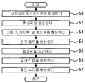
도 3은 본 발명의 실시형태 1에 관한 반도체장치의 제조방법을 나타낸 흐름도이다.
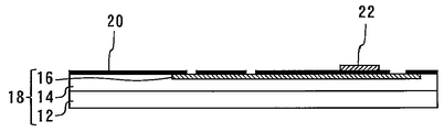
도 4는 질화막에 폴리실리콘이 형성된 상태를 도시한 도면이다.
도 5는 희생막이 형성된 상태를 도시한 도면이다.
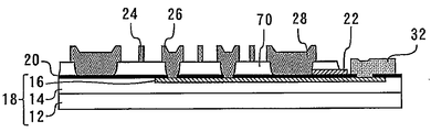
도 6은 가동부, 지지부, 및 봉지부가 형성된 상태를 도시한 도면이다.
도 7은 전극 패드가 형성된 상태를 도시한 도면이다.
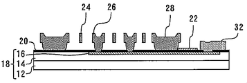
도 8은 희생막이 불산에 의해 에칭된 상태를 도시한 도면이다.
도 9는 유리 캡이 부착된 상태를 도시한 도면이다.
도 10은 본 발명의 실시형태 1에 관한 반도체장치의 변형예를 나타낸 평면도이다.
도 11은 본 발명의 실시형태 1에 관한 반도체장치의 변형예를 나타낸 평면도이다.
도 12는 본 발명의 실시형태 2에 관한 반도체장치의 단면도이다.1 is a cross-sectional view of a semiconductor device according to Embodiment 1 of the present invention.
2 is a plan view of a semiconductor device according to Embodiment 1 of the present invention.
3 is a flowchart showing a method of manufacturing a semiconductor device according to Embodiment 1 of the present invention.
4 is a diagram illustrating a state in which polysilicon is formed on a nitride film.
5 is a diagram illustrating a state in which a sacrificial film is formed.
6 is a view showing a state in which the movable portion, the support portion, and the encapsulation portion are formed.
7 is a diagram illustrating a state in which electrode pads are formed.
8 is a diagram illustrating a state in which a sacrificial film is etched by hydrofluoric acid.
9 is a view illustrating a state in which a glass cap is attached.
10 is a plan view showing a modification of the semiconductor device according to Embodiment 1 of the present invention.
11 is a plan view showing a modification of the semiconductor device according to Embodiment 1 of the present invention.
12 is a sectional view of a semiconductor device according to Embodiment 2 of the present invention.
실시형태 1.Embodiment 1
도 1은 본 발명의 실시형태 1에 관한 반도체장치의 단면도이다. 반도체장치(10)는 가속도 센서로 구성되어 있다. 반도체장치(10)는 Si 판(12)을 구비하고 있다. Si 판(12) 위에는 절연막(14)이 형성되어 있다. 절연막(14) 위에는 배선층(16)이 형성되어 있다. 절연막(14)의 표면과 배선층(16)의 표면은, 단차가 없게 접속되어 있다. 이때, Si 판(12), 절연막(14) 및 배선층(16)은 합쳐서 기판(18)으로 부르는 일이 있다.1 is a cross-sectional view of a semiconductor device according to Embodiment 1 of the present invention. The
절연막(14) 위와 배선층(16) 위에는 질화막(20)이 형성되어 있다. 질화막(20)은 배선층(16)의 일부를 노출시키도록 개구를 갖고 있다. 질화막(20) 위에는 폴리실리콘(22)이 형성되어 있다. 폴리실리콘(22)에는, 압축응력이 잔존하고 있다.The
반도체장치(10)에는, 가속도 센서의 대들보가 되는 가동부(24)가 형성되어 있다. 또한, 가동부(24)를 지지하는 지지부(26)가 형성되어 있다. 지지부(26)는, 질화막(20)의 개구를 통해 배선층(16)과 접하고 있다. 질화막(20) 위에는, 가동부(24)와 지지부(26)를 둘러싸도록 봉지부(28)가 형성되어 있다. 봉지부(28) 위에는 글래스 캡(30)이 고정되어 있다. 봉지부(28)와 글래스 캡(30)에 의해 공간(34)이 확보되어 있다. 공간(34) 내부에는 전술한 가동부(24)와 지지부(26)가 봉지되어 있다. 이때, 가동부(24), 지지부(26), 봉지부(28), 및 글래스 캡(30)은 합쳐서 센서부로 부르는 일이 있다.In the
질화막(20) 위에는 전극 패드(32)가 형성되어 있다. 전극 패드(32)는 외부와의 전기적 접속을 취하기 위해 형성되어 있다. 전극 패드(32)의 일부는 질화막(20)의 개구를 통해 배선층(16)과 접하고 있다. 따라서 전극 패드(32)와 지지부(26)는 배선층(16)을 통해 전기적으로 접속되어 있다. 그리고, 폴리실리콘(22), 센서부, 및 전극 패드(32)를 덮도록 몰드 수지(36)가 형성되어 있다. 몰드 수지(36)는 센서부 및 전극 패드(32)를 수분이나 이물질 등으로부터 보호하기 위해 형성되어 있다.The
도 2는 본 발명의 실시형태 1에 관한 반도체장치의 평면도이다. 도 2에서는 몰드 수지(36)의 표시를 생략하고 있다. 도 2에 나타낸 것과 같이, 전술한 폴리실리콘(22)은 센서부와 전극 패드(32) 사이, 및 전극 패드(32)끼리의 사이에 형성되어 있다.2 is a plan view of a semiconductor device according to Embodiment 1 of the present invention. In FIG. 2, the display of the
도 3은 본 발명의 실시형태 1에 관한 반도체장치의 제조방법을 나타낸 흐름도이다. 도 3에 따라 반도체장치(10)의 제조방법에 대해 설명한다. 우선, 질화막(20) 위에 폴리실리콘(22)이 형성된다(스텝 50). 도 4는 질화막(20) 위에 폴리실리콘(22)이 형성된 상태를 도시한 도면이다.3 is a flowchart showing a method of manufacturing a semiconductor device according to Embodiment 1 of the present invention. The manufacturing method of the
이어서, 질화막(20) 위에 희생막(70)이 형성된다(스텝 52). 희생막(70)은 가동부(24), 지지부(26), 및 봉지부(28)의 형상을 결정하기 위해 이용되고, 그후 제거되는 막이다. 도 5는 희생막(70)이 형성된 상태를 도시한 도면이다.Subsequently, a
이어서, 가동부(24), 지지부(26), 및 봉지부(28)가 형성된다(스텝 54). 가동부(24), 지지부(26), 및 봉지부(28)는 모두 도체다. 도 6은 가동부(24), 지지부(26), 및 봉지부(28)가 형성된 상태를 도시한 도면이다. 이어서 전극 패드(32)가 형성된다(스텝 56). 도 7은 전극 패드(32)가 형성된 상태를 도시한 도면이다.Next, the
이어서, 희생막(70)이 제거된다(스텝 58). 희생막(70)은 불산에 의한 에칭에 의해 제거된다. 이때, 폴리실리콘(22)은 불산처리에서 에칭되지 않고 잔존한다. 도 8은 희생막(70)이 불산에 의해 에칭된 상태를 도시한 도면이다.Subsequently, the
이어서, 봉지부(28) 위에 글래스 캡(30)이 부착된다(스텝 60). 도 9는 글래스 캡(30)이 부착된 상태를 도시한 도면이다. 최후에, 몰드 수지(36)가 형성된다(스텝 62). 상기한 제조방법에 의해 도 1에 나타낸 반도체장치(10)가 제조된다.Next, the
그런데, 질화막에는 강한 인장응력이 잔존하기 때문에, 질화막 위에 몰드 수지를 형성하면 몰드 수지가 박리하는 일이 있었다. 그러나, 본 발명의 실시형태 1에 관한 반도체장치(10)에 따르면 몰드 수지의 박리를 방지할 수 있다. 즉, 인장응력이 잔류하는 질화막(20) 위에, 압축응력이 잔류하는 폴리실리콘(22)이 형성되어 있기 때문에, 양자의 응력은 상쇄되어 약해진다. 그리고, 몰드 수지(36)는 응력이 약한 폴리실리콘(22) 위에 형성되어 있다. 따라서 질화막(20)을 형성하면서, 몰드 수지(36)의 박리를 방지할 수 있다.By the way, since strong tensile stress remain | survives in a nitride film, when mold resin was formed on a nitride film, the mold resin might peel. However, according to the
도 2를 참조해서 설명한 것과 같이, 폴리실리콘(22)은, 센서부와 전극 패드(32)의 사이, 및 전극 패드(32)끼리의 사이에 형성되어 있다. 따라서, 본 발명의 실시형태 1에 관한 반도체장치(10)에 따르면, 센서부와 전극 패드(32)의 사이에 있어서의 몰드 수지의 박리를 방지할 수 있다. 이 때문에, 센서부와 전극 패드(32) 사이의 쇼트를 방지할 수 있다. 또한, 전극 패드(32)의 사이의 몰드 수지의 박리를 방지할 수 있으므로 전극 패드(32) 사이의 쇼트도 방지할 수 있다.As described with reference to FIG. 2, the
몰드 수지의 박리 방지를 위해서는, 몰드 수지와 그것에 접하는 재료의 선팽창 계수에 대해서도 고려해야 한다. 본 발명의 실시형태 1에 관한 반도체장치(10)에서는, 몰드 수지(36), 폴리실리콘(22), 질화막(20)의 선팽창 계수는 각각 17[ppm/K], 2.5[ppm/K], 2.8[ppm/K] 정도이다. 몰드 수지(36)와 그것에 접하는 폴리실리콘(22) 및 질화막(20)의 선팽창 계수는 근사한 값이기 때문, 선팽창 계수의 괴리에 의한 몰드 수지의 박리를 방지할 수 있다.In order to prevent peeling of the mold resin, the linear expansion coefficient of the mold resin and the material in contact with the mold resin should also be considered. In the
폴리실리콘(22)은 불산에 의해 에칭되지 않는 재료이다. 그 때문에, 불산처리 전에 폴리실리콘(22)을 형성할 수 있다. 이에 따라 질화막(20) 형성후의 표면이 거의 평탄한 상태에 있어서 폴리실리콘(22)을 형성할 수 있기 때문에, 폴리실리콘(22)의 패터닝 등의 가공을 용이하게 할 수 있다.
도 10은 본 발명의 실시형태 1에 관한 반도체장치의 변형예를 나타낸 평면도이다. 폴리실리콘(72)은 전극 패드(32)를 둘러싸도록 형성되어 있다. 따라서, 전극 패드(32)의 주변에 있어서의 몰드 수지의 박리를 방지할 수 있다. 도 11은 본 발명의 실시형태 1에 관한 반도체장치의 변형예를 나타낸 평면도이다. 폴리실리콘(74)은, 전극 패드(32)와 센서부를 둘러싸도록 형성되어 있다. 따라서, 전극 패드(32)의 주변, 및 센서부의 주변에 있어서의 몰드 수지의 박리를 방지할 수 있다.10 is a plan view showing a modification of the semiconductor device according to Embodiment 1 of the present invention. The
반도체장치(10)는 가속도 센서로 형성했지만, 본 발명은 이것에 한정되지 않는다. 즉, 본 발명은 질화막 위에 몰드 수지를 형성하는 경우에 널리 응용할 수 있다. 또한, 본 발명의 실시형태 1에 있어서의 센서부는, 어떠한 소자이든 특별히 한정되지 않는다.Although the
본 발명의 실시형태 1에 관한 반도체장치(10)에서는, 몰드 수지(36)의 박리를 방지하는 박리 방지막으로서 폴리실리콘(22)을 사용했지만, 본 발명은 이것에 한정되지 않는다. 박리 방지막에 요구되는 특성은, 압축응력이 잔류하고 있을 것, 선팽창 계수가 질화막 및 몰드 수지의 선팽창 계수와 근사할 것, 불산으로 에칭되지 않을 것이다. 박리 방지막은 이들 특성을 갖는 한 특별히 한정되지 않는다. 따라서, 예를 들면, 아모퍼스 실리콘 막을 박리 방지막으로서 사용할 수 있다. 이때, 불산처리 전에 박리 방지막을 형성할 필요가 없을 때는, 박리 방지막은 불산에 의해 에칭되는 재료이어도 된다.
In the
실시형태 2.Embodiment 2 Fig.
도 12는 본 발명의 실시형태 2에 관한 반도체장치의 단면도이다. 반도체장치(76)에 대해서는, 본 발명의 실시형태 1에 관한 반도체장치(10)와 유사점이 많기 때문에, 반도체장치(10)와의 차이점만 설명한다. 반도체장치(76)는, 폴리실리콘(78)을 구비한다. 폴리실리콘(78)은 센서 부분과 전극 패드(32)의 사이 뿐만 아니라, 봉지부(28)의 바로 아래에도 형성되어 있다. 이에 따라 봉지부(28)와 배선층(16) 사이에는, 질화막(20)과 폴리실리콘(78)이 형성되어 있게 된다.12 is a sectional view of a semiconductor device according to Embodiment 2 of the present invention. Since the
본 발명의 실시형태 2에 관한 반도체장치에 따르면, 질화막(20)에 핀홀 등의 결함이 있었다고 하더라도, 그후에 해당 핀홀을 덮도록 고저항의 폴리실리콘(78)이 형성된다. 따라서, 봉지부(28)의 바로 아래 영역에 배선층(16)이 형성되어 있어도, 양자 사이의 쇼트를 확실하게 방지할 수 있다. 이때, 반도체장치(76)는, 본 발명의 실시형태 1과 같은 정도의 변형이 가능하다.According to the semiconductor device according to Embodiment 2 of the present invention, even if the
10 반도체장치, 18 기판, 20 질화막, 22 폴리실리콘, 36 몰드 수지10 semiconductor device, 18 substrate, 20 nitride film, 22 polysilicon, 36 mold resin
Claims (8)
상기 기판 위에 형성된 소자와,
상기 기판 위에 형성된 질화막과,
상기 질화막 위에 형성된 박리 방지막과,
상기 박리 방지막과 상기 소자를 덮도록 형성된 몰드 수지를 구비하고,
상기 박리 방지막은 압축응력이 잔류한 막인 것을 특징으로 하는 반도체장치.
Substrate,
An element formed on the substrate,
A nitride film formed on the substrate;
A peeling prevention film formed on the nitride film;
And a mold resin formed to cover the peeling preventing film and the element,
And said peeling preventing film is a film in which compressive stress remains.
상기 기판 위에 형성되고, 또한 상기 몰드 수지로 덮인 복수의 전극 패드를 구비하고,
상기 박리 방지막은, 상기 소자와 상기 복수의 전극 패드의 사이, 및 상기 복수의 전극 패드의 사이에 형성된 것을 특징으로 하는 반도체장치.
The method of claim 1,
A plurality of electrode pads formed on the substrate and covered with the mold resin;
The peeling preventing film is formed between the element and the plurality of electrode pads and between the plurality of electrode pads.
상기 기판 위에 형성되고, 또한 상기 몰드 수지로 덮인 복수의 전극 패드를 구비하고,
상기 박리 방지막은, 상기 복수의 전극 패드를 둘러싸도록 형성된 것을 특징으로 하는 반도체장치.
The method of claim 1,
A plurality of electrode pads formed on the substrate and covered with the mold resin;
The peeling preventing film is formed so as to surround the plurality of electrode pads.
상기 기판 위에 형성되고, 또한 상기 몰드 수지로 덮인 복수의 전극 패드를 구비하고,
상기 박리 방지막은, 상기 복수의 전극 패드와 상기 소자를 둘러싸도록 형성된 것을 특징으로 하는 반도체장치.
The method of claim 1,
A plurality of electrode pads formed on the substrate and covered with the mold resin;
The peeling preventing film is formed so as to surround the plurality of electrode pads and the element.
상기 소자는 가속도 센서의 센서부이고,
상기 기판 내에는 배선층이 형성되고,
상기 센서부와 상기 복수의 전극 패드는 상기 배선층에 의해 전기적으로 접속되고,
상기 박리 방지막은 불산에 의해 에칭되지 않는 막인 것을 특징으로 하는 반도체장치.
The method according to any one of claims 2 to 4,
The device is a sensor portion of the acceleration sensor,
A wiring layer is formed in the substrate,
The sensor unit and the plurality of electrode pads are electrically connected by the wiring layer,
And the peeling preventing film is a film which is not etched by hydrofluoric acid.
상기 소자는, 상기 박리 방지막 위에 형성된 도체를 구비하고,
상기 기판 중, 상기 도체의 바로 아래 영역에는 배선층이 형성된 것을 특징으로 하는 반도체장치.
The method of claim 1,
The element comprises a conductor formed on the peeling prevention film,
And a wiring layer is formed in a region immediately below the conductor of the substrate.
상기 박리 방지막은 폴리실리콘 또는 아모퍼스 실리콘으로 형성된 것을 특징으로 하는 반도체장치.
The method of claim 1,
The peeling preventing film is a semiconductor device, characterized in that formed of polysilicon or amorphous silicon.
상기 질화막 위에 폴리실리콘을 형성하는 공정과,
상기 질화막 위에 불산으로 제거할 수 있는 희생막을 형성하는 공정과,
상기 희생막을 이용해서 도체를 형성하는 공정과,
상기 희생막을 불산에 의해 제거하는 공정과,
상기 폴리실리콘 위에 몰드 수지를 형성하는 공정을 구비한 것을 특징으로 하는 반도체장치의 제조방법.Forming a nitride film on the substrate;
Forming polysilicon on the nitride film;
Forming a sacrificial film that can be removed with hydrofluoric acid on the nitride film;
Forming a conductor using the sacrificial film,
Removing the sacrificial film by hydrofluoric acid,
And a step of forming a mold resin on the polysilicon.
Applications Claiming Priority (2)
| Application Number | Priority Date | Filing Date | Title |
|---|---|---|---|
| JPJP-P-2010-131964 | 2010-06-09 | ||
| JP2010131964A JP5540911B2 (en) | 2010-06-09 | 2010-06-09 | Semiconductor device |
Publications (1)
| Publication Number | Publication Date |
|---|---|
| KR20110134830A true KR20110134830A (en) | 2011-12-15 |
Family
ID=45020205
Family Applications (1)
| Application Number | Title | Priority Date | Filing Date |
|---|---|---|---|
| KR1020110052558A KR20110134830A (en) | 2010-06-09 | 2011-06-01 | Semiconductor device and method of manufacture thereof |
Country Status (6)
| Country | Link |
|---|---|
| US (1) | US8390121B2 (en) |
| JP (1) | JP5540911B2 (en) |
| KR (1) | KR20110134830A (en) |
| CN (1) | CN102280416B (en) |
| DE (1) | DE102011075365B4 (en) |
| TW (1) | TWI431731B (en) |
Families Citing this family (10)
| Publication number | Priority date | Publication date | Assignee | Title |
|---|---|---|---|---|
| CN103890932B (en) * | 2011-11-22 | 2017-03-29 | 富士通株式会社 | Electronic unit and its manufacture method |
| US9025294B2 (en) * | 2012-02-24 | 2015-05-05 | Hamilton Sundstrand Corporation | System and method for controlling solid state circuit breakers |
| US9176089B2 (en) | 2013-03-29 | 2015-11-03 | Stmicroelectronics Pte Ltd. | Integrated multi-sensor module |
| US9082681B2 (en) | 2013-03-29 | 2015-07-14 | Stmicroelectronics Pte Ltd. | Adhesive bonding technique for use with capacitive micro-sensors |
| US9618653B2 (en) | 2013-03-29 | 2017-04-11 | Stmicroelectronics Pte Ltd. | Microelectronic environmental sensing module |
| GB2514547A (en) * | 2013-05-23 | 2014-12-03 | Melexis Technologies Nv | Packaging of semiconductor devices |
| US9000542B2 (en) * | 2013-05-31 | 2015-04-07 | Stmicroelectronics Pte Ltd. | Suspended membrane device |
| US10254261B2 (en) | 2016-07-18 | 2019-04-09 | Stmicroelectronics Pte Ltd | Integrated air quality sensor that detects multiple gas species |
| US10429330B2 (en) | 2016-07-18 | 2019-10-01 | Stmicroelectronics Pte Ltd | Gas analyzer that detects gases, humidity, and temperature |
| US10557812B2 (en) | 2016-12-01 | 2020-02-11 | Stmicroelectronics Pte Ltd | Gas sensors |
Family Cites Families (21)
| Publication number | Priority date | Publication date | Assignee | Title |
|---|---|---|---|---|
| JP2649157B2 (en) | 1987-03-10 | 1997-09-03 | 三菱電機株式会社 | Semiconductor device |
| JPH06104268A (en) | 1992-09-21 | 1994-04-15 | Mitsubishi Electric Corp | Semiconductor substrate having gettering effect and its manufacturing method |
| JPH06267935A (en) * | 1993-03-12 | 1994-09-22 | Mitsubishi Electric Corp | Manufacture of semiconductor device |
| JPH07297560A (en) | 1994-04-28 | 1995-11-10 | Hitachi Ltd | Multilayer printed wiring board and its mounting structure |
| JPH08178768A (en) * | 1994-12-20 | 1996-07-12 | Matsushita Electric Ind Co Ltd | Sensor for mechanical quantity |
| JPH08316442A (en) * | 1995-05-24 | 1996-11-29 | Mitsubishi Materials Corp | Soi substrate and its manufacture |
| JP3050193B2 (en) * | 1997-11-12 | 2000-06-12 | 日本電気株式会社 | Semiconductor device and manufacturing method thereof |
| US6049365A (en) * | 1998-05-07 | 2000-04-11 | Mitsubishi Denki Kabushiki Kaisha | Liquid crystal displaying apparatus with a converter not exposed to liquid crystal |
| JP2001119040A (en) | 1999-10-18 | 2001-04-27 | Denso Corp | Semiconductor amount-of-dynamics sensor and manufacturing method therefor |
| KR100514240B1 (en) | 2001-06-21 | 2005-09-13 | 미쓰비시덴키 가부시키가이샤 | Acceleration sensor and method of manufacturure thereof |
| JP2003240797A (en) * | 2002-02-18 | 2003-08-27 | Mitsubishi Electric Corp | Semiconductor acceleration sensor |
| WO2004105237A1 (en) | 2003-05-26 | 2004-12-02 | Murata Manufacturing Co., Ltd. | Piezoelectric electronic component, and production method therefor, communication equipment |
| JP4608993B2 (en) * | 2004-08-06 | 2011-01-12 | ソニー株式会社 | Micro electromechanical element, method for manufacturing the same, and electronic apparatus |
| JP2006310508A (en) | 2005-04-28 | 2006-11-09 | Sanyo Electric Co Ltd | Semiconductor device and its manufacturing method |
| DE102005028704B4 (en) | 2005-06-20 | 2016-09-08 | Infineon Technologies Ag | A method of manufacturing a semiconductor device having semiconductor device components embedded in plastic package |
| JP4633574B2 (en) | 2005-08-08 | 2011-02-16 | 三菱電機株式会社 | Thin film structure and manufacturing method thereof |
| JP2007274096A (en) * | 2006-03-30 | 2007-10-18 | Yamaha Corp | Diaphragm and its production process |
| JP2007322271A (en) * | 2006-06-01 | 2007-12-13 | Mitsubishi Electric Corp | Inertial force sensor and manufacturing method of the same |
| EP2065929A4 (en) * | 2006-09-06 | 2011-07-06 | Hitachi Metals Ltd | Semiconductor sensor device and method for manufacturing same |
| JP5181452B2 (en) | 2006-09-29 | 2013-04-10 | 三菱電機株式会社 | Acceleration sensor |
| JP2009016717A (en) * | 2007-07-09 | 2009-01-22 | Mitsubishi Electric Corp | Semiconductor device and method of manufacturing the same |
-
2010
- 2010-06-09 JP JP2010131964A patent/JP5540911B2/en active Active
-
2011
- 2011-02-09 TW TW100104251A patent/TWI431731B/en active
- 2011-02-11 US US13/025,633 patent/US8390121B2/en active Active
- 2011-05-05 DE DE102011075365.6A patent/DE102011075365B4/en active Active
- 2011-06-01 KR KR1020110052558A patent/KR20110134830A/en not_active Application Discontinuation
- 2011-06-08 CN CN201110165501.1A patent/CN102280416B/en active Active
Also Published As
| Publication number | Publication date |
|---|---|
| DE102011075365B4 (en) | 2016-06-09 |
| JP2011258751A (en) | 2011-12-22 |
| US20110303992A1 (en) | 2011-12-15 |
| DE102011075365A1 (en) | 2011-12-15 |
| CN102280416B (en) | 2014-04-09 |
| US8390121B2 (en) | 2013-03-05 |
| JP5540911B2 (en) | 2014-07-02 |
| TWI431731B (en) | 2014-03-21 |
| TW201208009A (en) | 2012-02-16 |
| CN102280416A (en) | 2011-12-14 |
Similar Documents
| Publication | Publication Date | Title |
|---|---|---|
| JP5540911B2 (en) | Semiconductor device | |
| US8776597B2 (en) | Capacitive type humidity sensor and manufacturing method thereof | |
| JP3613838B2 (en) | Manufacturing method of semiconductor device | |
| US6441481B1 (en) | Hermetically sealed microstructure package | |
| CN101667548A (en) | Temperature sensor with buffer layer | |
| US20060160264A1 (en) | Methods and apparatus having wafer level chip scale package for sensing elements | |
| CN105565256A (en) | Microintegrated encapsulated mems sensor with mechanical decoupling and manufacturing process thereof | |
| TW201036120A (en) | Exposed pad backside pressure sensor package | |
| JP2011258751A5 (en) | ||
| US20110127620A1 (en) | Mems integrated chip and method for making same | |
| US9546089B1 (en) | Pressure sensor and packaging method thereof | |
| US8937380B1 (en) | Die edge protection for pressure sensor packages | |
| JP2010203857A (en) | Package structure of pressure sensor | |
| US9302907B2 (en) | Micro-electro-mechanical-system device with guard ring and method for making same | |
| CN105489567A (en) | Semiconductor device | |
| KR200456132Y1 (en) | Sensor element protected by film layer and resin layer | |
| US9449897B2 (en) | Chip package and method for forming the same | |
| KR100787217B1 (en) | Mems structure and method for manufacturing thereof | |
| US20150349242A1 (en) | Conductive pad structure and method of fabricating the same | |
| JP2010147227A (en) | Electronic device package | |
| JP2008292182A (en) | Hall sensor | |
| JP2010237095A (en) | Capacitive humidity sensor and method of manufacturing the same | |
| CN109103152B (en) | Power device and packaging method thereof | |
| JP2011064509A (en) | Humidity sensor package, and method for manufacturing the same | |
| TWI712177B (en) | Micromechanical pressure sensor |
Legal Events
| Date | Code | Title | Description |
|---|---|---|---|
| A201 | Request for examination | ||
| E902 | Notification of reason for refusal | ||
| E601 | Decision to refuse application | ||
| J201 | Request for trial against refusal decision | ||
| J301 | Trial decision |
Free format text: TRIAL DECISION FOR APPEAL AGAINST DECISION TO DECLINE REFUSAL REQUESTED 20130731 Effective date: 20141017 |