KR20110052588A - Optoelectronic device for reducing the effects of concentrators shielding off the electrodes - Google Patents
Optoelectronic device for reducing the effects of concentrators shielding off the electrodes Download PDFInfo
- Publication number
- KR20110052588A KR20110052588A KR1020117002206A KR20117002206A KR20110052588A KR 20110052588 A KR20110052588 A KR 20110052588A KR 1020117002206 A KR1020117002206 A KR 1020117002206A KR 20117002206 A KR20117002206 A KR 20117002206A KR 20110052588 A KR20110052588 A KR 20110052588A
- Authority
- KR
- South Korea
- Prior art keywords
- optical
- semiconductor chip
- radiation
- contact
- members
- Prior art date
Links
- 230000005693 optoelectronics Effects 0.000 title claims abstract description 14
- 230000000694 effects Effects 0.000 title description 4
- 230000003287 optical effect Effects 0.000 claims abstract description 119
- 230000005855 radiation Effects 0.000 claims abstract description 117
- 239000004065 semiconductor Substances 0.000 claims abstract description 91
- 239000011521 glass Substances 0.000 claims description 7
- 230000000737 periodic effect Effects 0.000 claims description 6
- 229910052710 silicon Inorganic materials 0.000 claims description 4
- 239000010703 silicon Substances 0.000 claims description 4
- 239000000463 material Substances 0.000 description 12
- 230000005540 biological transmission Effects 0.000 description 7
- 230000015572 biosynthetic process Effects 0.000 description 5
- 238000005755 formation reaction Methods 0.000 description 5
- 239000011248 coating agent Substances 0.000 description 4
- 238000000576 coating method Methods 0.000 description 4
- XUIMIQQOPSSXEZ-UHFFFAOYSA-N Silicon Chemical compound [Si] XUIMIQQOPSSXEZ-UHFFFAOYSA-N 0.000 description 3
- 229910052782 aluminium Inorganic materials 0.000 description 3
- 150000001875 compounds Chemical class 0.000 description 3
- 230000018109 developmental process Effects 0.000 description 3
- 229910052751 metal Inorganic materials 0.000 description 3
- 239000002184 metal Substances 0.000 description 3
- 239000007787 solid Substances 0.000 description 3
- 239000000203 mixture Substances 0.000 description 2
- 229910052698 phosphorus Inorganic materials 0.000 description 2
- 240000001973 Ficus microcarpa Species 0.000 description 1
- 238000010521 absorption reaction Methods 0.000 description 1
- 230000032683 aging Effects 0.000 description 1
- 229910052785 arsenic Inorganic materials 0.000 description 1
- 239000004020 conductor Substances 0.000 description 1
- 239000013078 crystal Substances 0.000 description 1
- 230000007423 decrease Effects 0.000 description 1
- 238000010586 diagram Methods 0.000 description 1
- 239000002019 doping agent Substances 0.000 description 1
- 230000004907 flux Effects 0.000 description 1
- 229910052733 gallium Inorganic materials 0.000 description 1
- 229910052732 germanium Inorganic materials 0.000 description 1
- GNPVGFCGXDBREM-UHFFFAOYSA-N germanium atom Chemical compound [Ge] GNPVGFCGXDBREM-UHFFFAOYSA-N 0.000 description 1
- 229910052738 indium Inorganic materials 0.000 description 1
- 239000004615 ingredient Substances 0.000 description 1
- 150000002736 metal compounds Chemical class 0.000 description 1
- 150000002739 metals Chemical class 0.000 description 1
- -1 nitride compound Chemical class 0.000 description 1
- 230000000704 physical effect Effects 0.000 description 1
- 239000004033 plastic Substances 0.000 description 1
- 229920003023 plastic Polymers 0.000 description 1
- 239000002096 quantum dot Substances 0.000 description 1
- 230000000717 retained effect Effects 0.000 description 1
- 238000000926 separation method Methods 0.000 description 1
- 238000004088 simulation Methods 0.000 description 1
Images


Classifications
-
- G—PHYSICS
- G02—OPTICS
- G02B—OPTICAL ELEMENTS, SYSTEMS OR APPARATUS
- G02B19/00—Condensers, e.g. light collectors or similar non-imaging optics
- G02B19/0004—Condensers, e.g. light collectors or similar non-imaging optics characterised by the optical means employed
- G02B19/0028—Condensers, e.g. light collectors or similar non-imaging optics characterised by the optical means employed refractive and reflective surfaces, e.g. non-imaging catadioptric systems
-
- H—ELECTRICITY
- H01—ELECTRIC ELEMENTS
- H01L—SEMICONDUCTOR DEVICES NOT COVERED BY CLASS H10
- H01L31/00—Semiconductor devices sensitive to infrared radiation, light, electromagnetic radiation of shorter wavelength or corpuscular radiation and specially adapted either for the conversion of the energy of such radiation into electrical energy or for the control of electrical energy by such radiation; Processes or apparatus specially adapted for the manufacture or treatment thereof or of parts thereof; Details thereof
- H01L31/04—Semiconductor devices sensitive to infrared radiation, light, electromagnetic radiation of shorter wavelength or corpuscular radiation and specially adapted either for the conversion of the energy of such radiation into electrical energy or for the control of electrical energy by such radiation; Processes or apparatus specially adapted for the manufacture or treatment thereof or of parts thereof; Details thereof adapted as photovoltaic [PV] conversion devices
- H01L31/054—Optical elements directly associated or integrated with the PV cell, e.g. light-reflecting means or light-concentrating means
-
- H—ELECTRICITY
- H01—ELECTRIC ELEMENTS
- H01L—SEMICONDUCTOR DEVICES NOT COVERED BY CLASS H10
- H01L33/00—Semiconductor devices having potential barriers specially adapted for light emission; Processes or apparatus specially adapted for the manufacture or treatment thereof or of parts thereof; Details thereof
- H01L33/48—Semiconductor devices having potential barriers specially adapted for light emission; Processes or apparatus specially adapted for the manufacture or treatment thereof or of parts thereof; Details thereof characterised by the semiconductor body packages
- H01L33/58—Optical field-shaping elements
-
- F—MECHANICAL ENGINEERING; LIGHTING; HEATING; WEAPONS; BLASTING
- F21—LIGHTING
- F21K—NON-ELECTRIC LIGHT SOURCES USING LUMINESCENCE; LIGHT SOURCES USING ELECTROCHEMILUMINESCENCE; LIGHT SOURCES USING CHARGES OF COMBUSTIBLE MATERIAL; LIGHT SOURCES USING SEMICONDUCTOR DEVICES AS LIGHT-GENERATING ELEMENTS; LIGHT SOURCES NOT OTHERWISE PROVIDED FOR
- F21K9/00—Light sources using semiconductor devices as light-generating elements, e.g. using light-emitting diodes [LED] or lasers
- F21K9/60—Optical arrangements integrated in the light source, e.g. for improving the colour rendering index or the light extraction
-
- G—PHYSICS
- G01—MEASURING; TESTING
- G01J—MEASUREMENT OF INTENSITY, VELOCITY, SPECTRAL CONTENT, POLARISATION, PHASE OR PULSE CHARACTERISTICS OF INFRARED, VISIBLE OR ULTRAVIOLET LIGHT; COLORIMETRY; RADIATION PYROMETRY
- G01J1/00—Photometry, e.g. photographic exposure meter
- G01J1/02—Details
- G01J1/04—Optical or mechanical part supplementary adjustable parts
- G01J1/0407—Optical elements not provided otherwise, e.g. manifolds, windows, holograms, gratings
- G01J1/0411—Optical elements not provided otherwise, e.g. manifolds, windows, holograms, gratings using focussing or collimating elements, i.e. lenses or mirrors; Aberration correction
-
- G—PHYSICS
- G01—MEASURING; TESTING
- G01J—MEASUREMENT OF INTENSITY, VELOCITY, SPECTRAL CONTENT, POLARISATION, PHASE OR PULSE CHARACTERISTICS OF INFRARED, VISIBLE OR ULTRAVIOLET LIGHT; COLORIMETRY; RADIATION PYROMETRY
- G01J1/00—Photometry, e.g. photographic exposure meter
- G01J1/02—Details
- G01J1/04—Optical or mechanical part supplementary adjustable parts
- G01J1/0407—Optical elements not provided otherwise, e.g. manifolds, windows, holograms, gratings
- G01J1/0422—Optical elements not provided otherwise, e.g. manifolds, windows, holograms, gratings using light concentrators, collectors or condensers
-
- H—ELECTRICITY
- H01—ELECTRIC ELEMENTS
- H01L—SEMICONDUCTOR DEVICES NOT COVERED BY CLASS H10
- H01L31/00—Semiconductor devices sensitive to infrared radiation, light, electromagnetic radiation of shorter wavelength or corpuscular radiation and specially adapted either for the conversion of the energy of such radiation into electrical energy or for the control of electrical energy by such radiation; Processes or apparatus specially adapted for the manufacture or treatment thereof or of parts thereof; Details thereof
- H01L31/04—Semiconductor devices sensitive to infrared radiation, light, electromagnetic radiation of shorter wavelength or corpuscular radiation and specially adapted either for the conversion of the energy of such radiation into electrical energy or for the control of electrical energy by such radiation; Processes or apparatus specially adapted for the manufacture or treatment thereof or of parts thereof; Details thereof adapted as photovoltaic [PV] conversion devices
- H01L31/054—Optical elements directly associated or integrated with the PV cell, e.g. light-reflecting means or light-concentrating means
- H01L31/0547—Optical elements directly associated or integrated with the PV cell, e.g. light-reflecting means or light-concentrating means comprising light concentrating means of the reflecting type, e.g. parabolic mirrors, concentrators using total internal reflection
-
- H—ELECTRICITY
- H01—ELECTRIC ELEMENTS
- H01L—SEMICONDUCTOR DEVICES NOT COVERED BY CLASS H10
- H01L33/00—Semiconductor devices having potential barriers specially adapted for light emission; Processes or apparatus specially adapted for the manufacture or treatment thereof or of parts thereof; Details thereof
-
- H—ELECTRICITY
- H01—ELECTRIC ELEMENTS
- H01L—SEMICONDUCTOR DEVICES NOT COVERED BY CLASS H10
- H01L2924/00—Indexing scheme for arrangements or methods for connecting or disconnecting semiconductor or solid-state bodies as covered by H01L24/00
- H01L2924/0001—Technical content checked by a classifier
- H01L2924/0002—Not covered by any one of groups H01L24/00, H01L24/00 and H01L2224/00
-
- H—ELECTRICITY
- H01—ELECTRIC ELEMENTS
- H01L—SEMICONDUCTOR DEVICES NOT COVERED BY CLASS H10
- H01L31/00—Semiconductor devices sensitive to infrared radiation, light, electromagnetic radiation of shorter wavelength or corpuscular radiation and specially adapted either for the conversion of the energy of such radiation into electrical energy or for the control of electrical energy by such radiation; Processes or apparatus specially adapted for the manufacture or treatment thereof or of parts thereof; Details thereof
- H01L31/02—Details
- H01L31/0224—Electrodes
- H01L31/022408—Electrodes for devices characterised by at least one potential jump barrier or surface barrier
- H01L31/022425—Electrodes for devices characterised by at least one potential jump barrier or surface barrier for solar cells
- H01L31/022433—Particular geometry of the grid contacts
-
- H—ELECTRICITY
- H01—ELECTRIC ELEMENTS
- H01L—SEMICONDUCTOR DEVICES NOT COVERED BY CLASS H10
- H01L33/00—Semiconductor devices having potential barriers specially adapted for light emission; Processes or apparatus specially adapted for the manufacture or treatment thereof or of parts thereof; Details thereof
- H01L33/36—Semiconductor devices having potential barriers specially adapted for light emission; Processes or apparatus specially adapted for the manufacture or treatment thereof or of parts thereof; Details thereof characterised by the electrodes
- H01L33/38—Semiconductor devices having potential barriers specially adapted for light emission; Processes or apparatus specially adapted for the manufacture or treatment thereof or of parts thereof; Details thereof characterised by the electrodes with a particular shape
-
- Y—GENERAL TAGGING OF NEW TECHNOLOGICAL DEVELOPMENTS; GENERAL TAGGING OF CROSS-SECTIONAL TECHNOLOGIES SPANNING OVER SEVERAL SECTIONS OF THE IPC; TECHNICAL SUBJECTS COVERED BY FORMER USPC CROSS-REFERENCE ART COLLECTIONS [XRACs] AND DIGESTS
- Y02—TECHNOLOGIES OR APPLICATIONS FOR MITIGATION OR ADAPTATION AGAINST CLIMATE CHANGE
- Y02E—REDUCTION OF GREENHOUSE GAS [GHG] EMISSIONS, RELATED TO ENERGY GENERATION, TRANSMISSION OR DISTRIBUTION
- Y02E10/00—Energy generation through renewable energy sources
- Y02E10/50—Photovoltaic [PV] energy
- Y02E10/52—PV systems with concentrators
Landscapes
- Engineering & Computer Science (AREA)
- Microelectronics & Electronic Packaging (AREA)
- Physics & Mathematics (AREA)
- General Physics & Mathematics (AREA)
- Computer Hardware Design (AREA)
- Power Engineering (AREA)
- Optics & Photonics (AREA)
- Condensed Matter Physics & Semiconductors (AREA)
- Electromagnetism (AREA)
- Manufacturing & Machinery (AREA)
- Spectroscopy & Molecular Physics (AREA)
- General Engineering & Computer Science (AREA)
- Led Device Packages (AREA)
- Photovoltaic Devices (AREA)
Abstract
광전 장치(1)가 제공되며, 상기 광전 장치는 복수 개의 광학 부재(4a)를 구비한 광학적 구조체(4)를 가지는 광학 장치(3) 및 접촉 구조체(6)를 가지는 복사 방출 또는 복사 수신 반도체칩(2)을 포함하며, 상기 접촉 구조체는 반도체칩(2)의 전기 접촉을 위해 복수 개의 접촉 부재(6a)를 구비하고 상기 광학적 구조체(4)와 수직으로 이격되어 있으며, 이때 접촉 부재(6a)는 접촉 구조체(6)가 광학적 구조체(4)의 평면에 영사될 때 광학적 부재(4a) 사이의 간극에 배치된다.An optoelectronic device 1 is provided, wherein the optoelectronic device has an optical device 3 having an optical structure 4 having a plurality of optical members 4a and a radiation emitting or radiation receiving semiconductor chip having a contact structure 6. (2), wherein the contact structure includes a plurality of contact members 6a for electrical contact of the semiconductor chip 2 and is spaced perpendicular to the optical structure 4, wherein the contact members 6a are provided. Is disposed in the gap between the optical members 4a when the contact structure 6 is projected onto the plane of the optical structure 4.
Description
광전 장치가 제공되며, 더욱 상세하게는 검출기 시스템, 가령 태양 전지나 프로젝터와 같은 에너지 생성 시스템에 적합한 광전 장치가 제공된다. 상기 프로젝터는 예를 들면 비머(beamer)가 있다.Optoelectronic devices are provided and, more particularly, optoelectronic devices suitable for detector systems, such as energy generation systems such as solar cells or projectors. The projector is for example a beamer.
본 특허 출원은 독일 특허 출원 10 2008 030819.6의 우선권을 청구하며, 그 공개내용은 참조로 포함된다.This patent application claims the priority of German patent application 10 2008 030819.6, the disclosure of which is incorporated by reference.
문헌 DE 10 2005 033005 A1에는 복수 개의 복사 방출 영역들로 분할된 활성 영역 및 복수 개의 볼록한 부분 영역들을 구비한 광전 칩이 기재되어 있으며, 이때 상기 복수 개의 볼록한 부분 영역들은 복사 방출 영역들보다 큰 래터럴 치수를 가진다. 복사 방출 영역과 볼록한 부분 영역간의 이러한 비율에 의해, 상기 영역들로부터 방출된 복사가 전반사의 임계각보다 작은 각으로 부분 영역들상에 도달하여, 복사 아웃커플링효율이 향상될 수 있다.Document DE 10 2005 033005 A1 describes an optoelectronic chip having an active area divided into a plurality of radiation emission regions and a plurality of convex partial regions, wherein the plurality of convex partial regions are larger in lateral dimensions than the radiation emission regions. Has By this ratio between the radiation emitting region and the convex partial region, the radiation emitted from the regions reaches the partial regions at an angle smaller than the critical angle of total reflection, so that the radiation outcoupling efficiency can be improved.
본 발명의 과제는 손실이 적은 광전 장치를 제공하는 것이다.An object of the present invention is to provide a photoelectric device with low loss.
바람직한 실시예에 따르면, 광전 장치는 복수 개의 광학 부재들을 구비한 광학적 구조체를 가진 광학 장치 및 복사 방출 또는 복사 수신 반도체칩을 포함하며, 상기 반도체칩은 상기 반도체칩의 전기 접촉을 위한 복수 개의 접촉 부재들을 구비한 접촉 구조체를 가지며, 상기 접촉 구조체는 광학적 구조체와 수직으로 이격되어 있다. 이때, 접촉 구조체가 광학적 구조체의 평면상에 영사될 때 접촉 부재들은 광학적 부재들사이의 간극에 배치된다.According to a preferred embodiment, the optoelectronic device comprises an optical device having an optical structure having a plurality of optical members and a radiation emitting or radiation receiving semiconductor chip, the semiconductor chip comprising a plurality of contact members for electrical contact of the semiconductor chip. And a contact structure having a plurality of contact structures, wherein the contact structure is vertically spaced apart from the optical structure. At this time, when the contact structure is projected on the plane of the optical structure, the contact members are disposed in the gap between the optical members.
상기의 수직 이격에 의해, 원하는 광학적 효과가 얻어질 수 있는데, 즉, 복사 수신 반도체칩의 복사 입사면에 있어서 접촉 구조체에 의해 서로 분리된 영역들에서 복사가 집속되거나, 상기 영역들로부터 출사되는 복사가 광학적 구조체에 의해 평행 정렬되도록 할 수 있다.By the above vertical separation, a desired optical effect can be obtained, i.e., radiation is focused or radiated from the regions separated from each other by the contact structure in the radiation incident surface of the radiation receiving semiconductor chip. Can be aligned parallel by the optical structure.
유리한 발전예에 따르면, 접촉 구조체는 반도체칩에서 광학적 장치를 향해있는 복사 투과면상에 제공된다. 복사 방출 반도체칩의 경우, 복사 투과면이 복사 출사면에 상응하는 반면, 복사 수신 반도체칩의 경우 복사 투과면은 복사 입사면을 나타낸다.According to an advantageous development, the contact structure is provided on a radiation transmissive surface facing the optical device in the semiconductor chip. In the case of the radiation emitting semiconductor chip, the radiation transmitting surface corresponds to the radiation emitting surface, while in the radiation receiving semiconductor chip, the radiation transmitting surface represents the radiation incident surface.
바람직하게는, 접촉 구조체는 반도체칩의 복사 투과면의 일부 영역들만을 덮는데, 즉 접촉 구조체에 의해 복사 투과면의 전면이 덮이지 않는다. 따라서, 본원의 불연속형 접촉 구조체의 경우, 접촉 구조체에서 복사가 흡수되어 발생하는 복사 손실이 감소한다.Preferably, the contact structure covers only some regions of the radiation transmissive surface of the semiconductor chip, ie the front surface of the radiation transmissive surface is not covered by the contact structure. Thus, in the case of the discontinuous contact structure of the present application, the radiation loss caused by the absorption of radiation in the contact structure is reduced.
또한, 바람직하게는, 광학적 구조체는 광학적 장치에서 접촉 구조체를 향해있는 복사 투과면상에 배치된다. 복사 방출 반도체칩의 경우 광학 장치의 복사 투과면이 광학 장치의 복사 입사면에 상응하는 반면, 복사 수신 반도체칩의 경우 복사 투과면은 광학 장치의 복사 출사면을 나타낸다.Also preferably, the optical structure is disposed on a radiation transmitting surface facing the contact structure in the optical device. In the case of the radiation emitting semiconductor chip, the radiation transmitting surface of the optical device corresponds to the radiation incident surface of the optical device, whereas in the radiation receiving semiconductor chip, the radiation transmitting surface represents the radiation exit surface of the optical device.
복사 수신 반도체칩의 경우, 광학적 구조체에 의해, 투과된 복사가 래터럴로 서로 분리된 복사 투과면의 영역들에서 모일 수 있고, 이때 상기 영역들 사이에서의 조도는 상대적으로 상당히 감소한다. 이러한 낮은 조도를 가진 간극 영역들에서는 접촉 구조체가 배치되는 것이 유리하다. 조도가 낮은 간극 영역들은 특히 광학 구조체의 광학적 부재들 사이의 간극에 대응된다. 접촉 구조체는 주 복사 경로의 밖에 위치하여, 접촉 구조체에 의한 차폐가 실질적으로 방지된다. 따라서, 복사 손실이 상당히 감소할 수 있다.In the case of a radiation receiving semiconductor chip, the optical structure allows the transmitted radiation to gather in regions of the radiant transmission surface which are separated from each other laterally, wherein the illuminance between the regions is relatively reduced. In such low roughness gap regions it is advantageous to place the contact structure. The low roughness gap regions correspond in particular to the gap between the optical members of the optical structure. The contact structure is located outside the main radiation path, so that shielding by the contact structure is substantially prevented. Thus, radiation loss can be significantly reduced.
유리하게는, 복사 방출 반도체칩의 경우, 광학적 구조체가 접촉 구조체를 "숨길"수 있어서, 반도체칩에서부터 보는 방향으로 광학적 장치보다 뒤에 배치되는 면은 균일하게 발광하고, 접촉 구조체에 의해 중도에 끊기지 않는다. 접촉 구조체에 의해 서로 분리된 발광 영역들이 생성되고, 상기 영역들은 광학적 장치 또는 광학적 구조체에 의해 균일하게 발광하는 하나의 면으로 합쳐진다.Advantageously, in the case of a radiation emitting semiconductor chip, the optical structure can "hide" the contact structure so that the surface disposed behind the optical device in the viewing direction from the semiconductor chip emits light uniformly and is not interrupted halfway by the contact structure. . The light emitting regions separated from each other by the contact structure are created, and the regions are merged into one surface which emits light uniformly by the optical device or the optical structure.
접촉 구조체는 전기 전도 물질을 함유한 구조화된 코팅의 형태로 반도체칩의 복사 투과면상에 제공될 수 있다. 상기 코팅은 특히 금속을 포함한다.The contact structure may be provided on the radiation transmissive surface of the semiconductor chip in the form of a structured coating containing an electrically conductive material. The coating in particular comprises a metal.
광학적 구조체는 복사 투과 물질로 형성될 수 있다. 적합한 물질은 예를 들면 유리이다. 유리는 단파 복사, 특히 자외 복사에 대해 상대적으로 양호한 시효 안정성을 가진다.The optical structure may be formed of a radiation transmitting material. Suitable materials are, for example, glass. Glass has a relatively good aging stability against shortwave radiation, in particular ultraviolet radiation.
광학적 구조체는 주기 구조를 가지는 것이 유리한데, 즉 광학적 구조체의 광학 부재들은 규칙적으로 배치된다.It is advantageous for the optical structure to have a periodic structure, ie the optical members of the optical structure are arranged regularly.
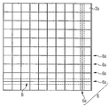
유리한 형성예에 따르면, 광학적 부재들은 렌즈 어레이 또는 광학 격자를 형성한다. 예를 들면, 렌즈 어레이는 규칙적으로 배치된 복수 개의 렌즈들을 포함할 수 있고, 상기 렌즈들은 반도체칩을 향한 측에서 볼록하게 만곡된 표면을 가진다. 특히, 반도체칩의 복사 방출 영역 또는 복사 수신 영역은 렌즈들의 초점들에 의해 펼쳐지는 평면에 위치하거나, 상기 평면에 근접하여 위치할 수 있다. 따라서, 광학적 구조체에 의해 반도체칩상에 도달하는 복사는 복사 수신 영역에 집속되는 반면, 반도체칩으로부터 방출된 복사는 광학적 구조체에 의해 평행하게 정렬된다.According to an advantageous formation, the optical members form a lens array or optical grating. For example, the lens array may include a plurality of lenses arranged regularly, the lenses having convexly curved surfaces on the side facing the semiconductor chip. In particular, the radiation emitting area or the radiation receiving area of the semiconductor chip may be located on a plane spread by the focal points of the lenses or may be located close to the plane. Thus, radiation reaching the semiconductor chip by the optical structure is focused on the radiation receiving area, while radiation emitted from the semiconductor chip is aligned in parallel by the optical structure.
광학적 구조체에 상응하여, 접촉 구조체도 주기 구조를 가질 수 있다. 특히, 접촉 구조체의 주기성은 광학적 구조체의 주기성과 일치하며, 즉 접촉 부재들은 광학적 부재들과 동일한 규칙성으로 배치된다.Corresponding to the optical structure, the contact structure may also have a periodic structure. In particular, the periodicity of the contact structure coincides with the periodicity of the optical structure, ie the contact members are arranged with the same regularity as the optical members.
유리한 형성예에 따르면, 접촉 구조체는 망의 형태로 배치된 접촉 부재들로 이루어진다. 접촉 부재들은 특히 접촉웹(contact web)일 수 있다. 바람직하게는, 광학적 구조체는 접촉 구조체의 간극이 있는 위치에서 광학적 부재들, 예를 들면 렌즈들을 포함한다.According to an advantageous formation, the contact structure consists of contact members arranged in the form of a net. The contact members can in particular be a contact web. Preferably, the optical structure comprises optical members, for example lenses, at the position of the gap of the contact structure.
바람직한 발전예에서, 광학적 장치는 집광기를 포함한다. 반도체칩을 향한 측에서, 집광기는 제1구경(aperture)을 포함하고, 상기 제1구경은 특히 반도체칩과 반대 방향을 향해있는 측에 배치된, 집광기의 제2구경보다 작다. 집광기를 이용하면, 조도가 충분한 경우에 칩 크기가 상대적으로 작게 유지될 수 있고, 이러한 점은 재료 비용을 낮춘다. 제2구경은 제1구경보다 약 10 내지 1000배 큰 것이 유리하거나, 바람직하게는 제1구경에 상응하는 반도체칩의 복사 투과면보다 약 10 내지 1000배 클 수 있다. 집광기의 길이는 제2구경 또는 제1구경 및 집광기의 개구각에 의해 정해진다.In a preferred development, the optical device comprises a light collector. On the side facing the semiconductor chip, the light collector comprises a first aperture, which is smaller than the second diameter of the light collector, in particular arranged on the side facing away from the semiconductor chip. With a light collector, the chip size can be kept relatively small if the illuminance is sufficient, which lowers the material cost. The second diameter may advantageously be about 10 to 1000 times larger than the first diameter, or preferably about 10 to 1000 times larger than the radiation transmission surface of the semiconductor chip corresponding to the first diameter. The length of the collector is determined by the second or first diameter and the opening angle of the collector.
광학적 장치의 유리한 형성예는 포물면 집광기를 고려한다. 포물면 집광기는 횡단면이 부분적인 포물선과 동일하고, 대칭축에 대해 이루는 특정한 각도 내에서 입사되는 복사가 한정된 면에 집속되거나 상기 면으로부터 출사되는 복사가 한정된 각도 범위로 방출된다는 특성을 가진다. 바람직하게는, 광학적 구조체는 제1구경의 영역에서 초점에 근접하여 배치된다.Advantageous formations of optical devices consider parabolic collectors. Parabolic condensers have the property that the cross section is the same as a partial parabola and that radiation incident within a certain angle with respect to the axis of symmetry is focused on a confined plane or radiation emitted from the plane is emitted in a confined angle range. Preferably, the optical structure is disposed proximate to the focal point in the region of the first aperture.
바람직한 실시예에 따르면, 집광기는 통몸체(solid body)로서, 상기 통몸체는 반도체칩을 향한 표면에서 광학적 구조체를 포함한다. 집광기와 광학적 구조체의 조합은 일체형으로 형성될 수 있으며, 이때 두 구성 요소는 동일한 물질, 예를 들면 유리를 포함하는 것이 바람직하다. 복사는 집광기에서 우선적으로, 외벽에서의 전반사에 의해 안내된다.According to a preferred embodiment, the collector is a solid body, which comprises an optical structure at the surface facing the semiconductor chip. The combination of the collector and the optical structure can be formed in one piece, with the two components preferably comprising the same material, for example glass. The radiation is guided primarily by the total reflection at the outer wall in the collector.
그러나, 집광기가 반사성 내부면을 구비한 중공체로서, 반도체칩을 향한 측에서 상기 집광기보다 뒤에 광학적 구조체가 배치되는 경우도 고려할 수 있다. 이때, 두 구성 요소는 동일한 물질로 제조되지 않은 2개의 별도 구성 요소인 것이 바람직하다. 중공체는 예를 들면 플라스틱 물질로 제조될 수 있고, 내부면에 반사성 코팅을 포함할 수 있다. 상기 코팅은 특히 금속을 함유한다. 광학적 구조체는 유리로 형성될 수 있다.However, it may also be considered that the collector is a hollow body having a reflective inner surface, in which an optical structure is disposed behind the collector at the side facing the semiconductor chip. In this case, the two components are preferably two separate components not made of the same material. The hollow body may for example be made of a plastics material and may comprise a reflective coating on the inner surface. The coating contains especially metals. The optical structure can be formed of glass.
유리한 발전예에 따르면, 반도체칩은 복사 방출 영역 또는 복사 수신 영역을 포함하고, 이러한 영역은 접촉 구조체에 의해 덮이지 않은 영역들에서 제 기능을 한다. 바람직하게는, 복사 방출 영역 또는 복사 수신 영역은 접촉 구조체에 의해 덮인 영역들에서도 제 기능을 발휘하며, 즉 기능 영역의 크기가 바람직하게는 복사 방출 영역 또는 복사 수신 영역의 전체 면의 합에 상응한다.According to an advantageous development, the semiconductor chip comprises a radiation emitting area or a radiation receiving area, which functions in areas not covered by the contact structure. Preferably, the radiation emitting area or the radiation receiving area also functions in the areas covered by the contact structure, ie the size of the functional area preferably corresponds to the sum of the entire faces of the radiation emitting area or the radiation receiving area. .
광학적 구조체 및 반도체칩이 수직으로 이격될 때의 그 간극은 광학적 구조체와는 다른 굴절률을 가지는 것이 유리하다. 예를 들면, 상기 간극에서는 공기(굴절률 n=1) 또는 실리콘(굴절률, 예를 들면 n=1.4)이 있을 수 있다. 광학적 구조체는 유리(굴절률, 예를 들면 n=1.5)로 형성될 수 있다.When the optical structure and the semiconductor chip are vertically spaced apart, it is advantageous that the gap has a refractive index different from that of the optical structure. For example, there may be air (refractive index n = 1) or silicon (refractive index, for example n = 1.4) in the gap. The optical structure can be formed of glass (refractive index, for example n = 1.5).
바람직한 형성예에 따르면, 복사 방출 반도체칩은 발광다이오드이다. 다른 형성예에 따르면, 복사 수신 반도체칩은 복사 검출기 또는 태양 전지이다. 반도체칩은 복사 방출 영역 또는 복사 수신 영역과 함께 복사를 생성하거나 수신하는 pn 접합을 포함한다. 이러한 pn 접합은 가장 간단한 경우에 p형 반도체층과 n형 반도체층을 이용하여 형성될 수 있고, 이러한 반도체층은 직접 접해있다. 바람직하게는, p형층과 n형층 사이에 고유의 복사 생성층 또는 복사 수신층이 형성된다. 특히, 복사 방출 반도체칩의 경우에 고유의 복사 생성층은 도핑되거나 도핑되지 않은 양자층의 형태로 형성될 수 있다. 양자층은 단일 양자 우물 구조(SQW, single quantum well) 또는 다중 양자 우물 구조(MQW, multipld quantum well) 또는 양자선 또는 양자점 구조로 형성될 수 있다.According to a preferred embodiment, the radiation emitting semiconductor chip is a light emitting diode. According to another formation, the radiation receiving semiconductor chip is a radiation detector or a solar cell. The semiconductor chip includes a pn junction for generating or receiving radiation along with a radiation emitting region or a radiation receiving region. This pn junction can be formed using the p-type semiconductor layer and the n-type semiconductor layer in the simplest case, and the semiconductor layer is in direct contact. Preferably, a unique radiation generating layer or radiation receiving layer is formed between the p-type layer and the n-type layer. In particular, in the case of a radiation emitting semiconductor chip, the intrinsic radiation generating layer may be formed in the form of a doped or undoped quantum layer. The quantum layer may be formed of a single quantum well structure (SQW) or a multi quantum well structure (MQW) or a quantum line or quantum dot structure.
복사 검출기로서 형성된 반도체칩은, 특히, 하나보다 많은 수의 복사 수신 영역을 포함할 수 있다. 복사 수신 영역들은 포개어져 배치될 수 있고, 서로 다른 파장의 복사를 흡수할 수 있다.A semiconductor chip formed as a radiation detector may, in particular, comprise more than one radiation receiving area. The radiation receiving regions can be superimposed and can absorb radiation of different wavelengths.
반도체칩을 위해 적합한 물질은, 특히, III-V 반도체이며, 특히 비화물 화합물 반도체, 인화물 화합물 반도체 또는 질화물 화합물 반도체로서, 이때 물질 조성은 AlnGamIn1-n-mAs, AlnGamIn1-n-mP 또는 AlnGamIn1-n-mN이며, 0≤n≤1, 0≤m≤1, 및 n+m≤1이다. 이때, 상기 물질은 상기 수식에 따라 수학적으로 정확한 조성을 반드시 포함할 필요는 없다. 오히려, 하나 이상의 도펀트 및 부가 성분을 포함할 수 있고, 이는 상기 물질의 물리적 특성을 실질적으로 변경하지 않는다. 그러나, 결정 격자의 핵심 성분(Al, Ga, In, P)만은 비록 이들이 미량의 다른 성분으로 일부 대체될 수 있다고 하더라도 상기 수식에 포함되는 것이 간단하다.Suitable materials for semiconductor chips are, in particular, III-V semiconductors, in particular arsenide compound semiconductors, phosphide compound semiconductors or nitride compound semiconductors, wherein the material composition is Al n Ga m In 1-nm As, Al n Ga m In 1-nm P or Al n Ga m In 1-nm N, where 0 ≦ n ≦ 1, 0 ≦ m ≦ 1, and n + m ≦ 1. In this case, the material does not necessarily include a mathematically correct composition according to the above formula. Rather, it may include one or more dopants and additional ingredients, which do not substantially alter the physical properties of the material. However, only the key components (Al, Ga, In, P) of the crystal lattice are simply included in the above formula, although they may be partially replaced by other components in trace amounts.
또한, 반도체칩은 규소와 같은 원소 반도체 또는 II-VI 화합물 반도체를 포함할 수 있고, 이러한 화합물 반도체는 태양 전지의 경우에 특히 적합하다. 또한, 복사 검출기의 경우 게르마늄은 제1복사 수신 영역을 위해 사용될 수 있고, 제2수신 영역은 III-V 반도체로 형성될 수 있다.In addition, the semiconductor chip may include an elemental semiconductor such as silicon or an II-VI compound semiconductor, which is particularly suitable for solar cells. Further, in the case of the radiation detector, germanium may be used for the first radiation receiving region, and the second receiving region may be formed of III-V semiconductor.
또한, 본원에서 "수직"이란, 광학적 구조체가 반도체칩보다 뒤에 배치될 때의 방향을 의미한다. "래터럴"이란 수직 방향에 대해 세로 방향을 의미할 수 있다.In addition, the term “vertical” herein means a direction when the optical structure is disposed behind the semiconductor chip. "Lateral" may mean a vertical direction with respect to the vertical direction.
이하, 상기에 기술한 광전 장치를 도 1 내지 7에 의거하여 더욱 상세히 설명한다.Hereinafter, the above-described photovoltaic device will be described in more detail with reference to FIGS. 1 to 7.
도 1은 광학적 장치의 효과를 설명하기 위해 광전 장치의 개략적 횡단면도를 도시한다.
도 2는 반도체칩, 광학적 구조체 및 집광기를 구비한 광전 장치의 개략적 횡단면도를 도시한다.
도 3은 광학적 구조체와 반도체칩 사이의 복사 경로를 설명하기 위해 반도체칩과 광학적 구조체의 개략적 횡단면도를 도시한다.
도 4는 반도체칩의 복사 투과면상에서의 세기 분포를 점 다이어그램으로 도시한다.
도 5는 반도체칩의 조사된 영역에서 포집된 에너지를 그래프로 도시한다.
도 6은 접촉 구조체의 개략적 평면도를 도시한다.
도 7은 복사 방출 반도체칩 또는 복사 수신 반도체칩의 개략적 횡단면도를 도시한다.1 shows a schematic cross-sectional view of an optoelectronic device to illustrate the effect of the optical device.
2 shows a schematic cross sectional view of a photovoltaic device with a semiconductor chip, an optical structure and a light collector.
3 shows a schematic cross-sectional view of a semiconductor chip and an optical structure to explain the radiation path between the optical structure and the semiconductor chip.
Fig. 4 shows in intensity diagram the intensity distribution on the radiation transmitting surface of the semiconductor chip.
5 graphically shows the energy collected in the irradiated region of the semiconductor chip.
6 shows a schematic plan view of a contact structure.
7 shows a schematic cross-sectional view of a radiation emitting semiconductor chip or a radiation receiving semiconductor chip.
동일하거나 동일한 효과를 가진 요소는 도면에서 동일한 참조번호를 가진다.Elements having the same or the same effect have the same reference numerals in the drawings.
도 1에는 복사 방출 반도체칩 또는 복사 수신 반도체칩(2)과 광학적 장치(3)를 구비한 광전 장치(1)가 도시되어 있다.1 shows a
도 1로부터 알 수 있는 바와 같이, 광학적 장치(3)는 반도체칩(2)을 향해있는 측에서 제1구경(A1)을 포함하고, 상기 제1구경은 반도체칩(2)과 반대 방향을 향하는 측에 배치된 제2구경(A2)보다 작다. 바람직하게는, 칩 크기는 제1구경(A1)의 크기에 맞춰지고, 특히 제1구경(A1)과 동일한 래터럴 치수를 가진다.As can be seen from FIG. 1, the
반도체칩(2)은 수평 단면이 직사각형이고, 특히 정사각형이며, 이때 상기 수평 단면적의 값은 0.0001 ㎠(100 ㎛ x 100 ㎛)과 10 ㎠사이에서 얻어질 수 있다. 하한값은 접촉 구조체의 제조 가능성 또는 효과에 의해 결정된다. 상한값은 광학적 장치의 구현 가능성에 의해 결정된다.The
제2구경(A2)의 적합한 크기는 예를 들면 100 ㎠이다. 유리하게는, 반도체칩(2)은 1 ㎠의 수평 단면적을 가진다. Suitable size of the second diameter A 2 is, for example, 100
복사 원뿔(radiation cone)의 개구각은 각(α)이라고 하고, 상기 복사 원뿔은 제2구경(A2)을 통해 광학적 장치(3)로부터 출사되거나, 제2구경(A2)을 통해 광학적 장치(3)로 입사된다. 복사원으로서 태양과 같은 원거리 복사원을 가정하는 경우, 각(α)은 상대적으로 작을 수 있고, 가령 1°(±0.5°)이다. 광학적 장치(3)에서 복사 원뿔의 각(α)은 각(β)에 비해 작아지고, 예를 들면 약 0.7°(±0.35°)이다. 광학적 장치(3)의 에텐듀(etendue)가 유지됨에 따라, 제1구경(1)에 도달하는 각(δ)은 제2구경(A2)에 도달하는 각(β)보다 큰데, 제1구경(1)은 제2구경(A2)보다 작기 때문이다. 이 경우, 각(δ)은 7°(±3.5°)이다. 입체각 인자는 100이다.The opening angle of the radiation cone (radiation cone) are each (α) is called, and the radiation cones optical device through or emitted from the
반도체칩(2)이 복사 수신기인 경우, 태양광은 1000 W/㎡의 조도로 제2구경(A2)을 통해 들어올 수 있어서, 반도체칩(2)의 1 ㎠ 크기의 복사 투과면상에는 10 W의 복사속이 얻어진다. 상기 제2구경은 이미 언급한 바와 같이 100 ㎠의 면적을 가질 수 있다.In the case where the
반도체칩(2)이 복사원인 경우, 광학적 장치(3)를 통해 비교적 낮은 발산도를 가진 복사가 방출될 수 있다. 그러므로, 광전 장치(1)는 프로젝터에 사용되기에 매우 적합하다.When the
도 2는 광학적 장치(3)의 가능한 형성예를 도시한다. 광학적 장치는 포물면형 집광기(5)를 포함할 수 있고, 상기 집광기는 입사된 복사를 가능한 한 손실없이 집광기 몸체를 통해 안내한다.2 shows a possible formation of the
집광기(5)는 예를 들면 통몸체일 수 있고, 상기 통몸체의 외벽에서 복사는 전반사됨에 따라 집광기(5)에 보유된다. 또는, 집광기(5)는 거울 코팅된 내부면을 구비한 중공체일 수 있다.The light collector 5 may be, for example, a barrel body, and radiation is retained in the collector 5 as total radiation is reflected on the outer wall of the barrel body. Alternatively, the light collector 5 may be a hollow body having a mirror coated inner surface.
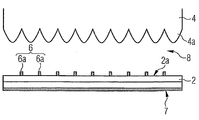
또한, 광학적 장치(3)는 반도체칩(2)을 향해있는 측에서 광학적 구조체(4)를 포함한다. 광학적 구조체(4)는, 바람직하게는 집광기(5)와 기계적으로 결합된 별도의 구성 요소일 수 있다. 또는, 광학적 구조체(4)는 집광기(5)와 일체형으로 형성될 수 있고, 즉, 광학적 구조체(4)와 집광기(5)가 하나의 작업 단계에서 바람직하게는 동일한 물질로 제조된다. 후자의 가능성은 집광기(5)가 통몸체인 경우에 적용되는 것이 바람직하다.The
광하적 구조체(4)는 주기 구조를 가지는 것이 유리하다. 도시된 바와 같이, 광학적 구조체(4)는 규칙적으로 배치된 복수 개의 광학적 부재들(4a)을 포함한다. 특히, 광학적 부재들(4a)은 볼록한 표면을 가진 렌즈들이다.It is advantageous for the
바람직하게는, 광학적 구조체(4)는 그 수평 단면이 반도체칩(2)의 수평 단면에 상응한다. 수평 단면적이 1 ㎠일 때, 광학적 구조체(4)는 예를 들면 ㎟ 당 하나의 광학 부재(4a)를 포함할 수 있고, 즉, 각각의 광학적 부재(4a)의 직경은 약 1 mm이다.Preferably, the
유리의 복사 투과도에 의해, 이러한 물질은 광학적 구조체(4)를 위해 사용되는 것이 유리할 수 있다.By virtue of the radiation transmission of the glass, it may be advantageous that such a material is used for the
도 3은 도 1 및 2에 도시된 광전 장치와 같은 장치의 일부를 확대하여 도시한다.3 shows an enlarged view of a portion of a device such as the photovoltaic device shown in FIGS. 1 and 2.
광학적 구조체(4)는 복수 개의 광학 부재들(4a)을 포함하고, 상기 광학 부재들은 특히 렌즈로 형성된다. 이는 이미 도 2와 관련하여 상세히 설명된 바 있다.The
도 3으로부터 알 수 있는 바와 같이, 각 광학 부재(4a)에 의해 생성된 광선속을 선분으로 나타낸 광빔은 수렴되거나, 복사 방출 반도체칩의 경우 발산해나간다. 반도체칩(2)상에 도달한 광선속 또는 반도체칩으로부터 방출된 광선속 사이에는 더 낮은 세기를 가진 영역(B)이 존재한다. 이러한 영역(B)에서 반도체칩(2)은 접촉 부재들(미도시)을 포함하고, 상기 접촉 부재들이 모여 하나의 접촉 구조체를 형성한다. 접촉 구조체는 바람직하게는 반도체칩(2)의 복사 투과면(2a)상에 배치된다.As can be seen from Fig. 3, the light beam representing the light beam generated by each
반도체칩(2) 또는 복사를 수신하거나 방출하는 영역은 광학적 부재들(4a)의 초점에 의해 펼쳐지는 평면에 직접적으로 배치될 필요는 없다. 반도체칩(2)은 상기 평면에 근접하여, 광학적 구조체(4)에 대해 약간의 작은 수직 간격(D)을 두어 배치될 수 있다. 광학적 구조체(4)와 반도체칩(2)간의 간격(D)은, 접촉 구조체에 의한 차폐 위험 없이 접촉 구조체가 충분히 크게 형성될 수 있을 만큼 크게 선택된다. 또한, 상기 간격은, 칩의 면을 이상적으로 활용하기 위해 상기 영역(B)이 충분한 치수를 가질 만큼 작게 선택된다.The
도 4는 도 1 내지 도 3에 따른 복사 수신 반도체칩(2)의 복사 투과면(2a)상에 도달할 수 있는 세기 분포의 모의 실험 결과를 도시한다.FIG. 4 shows simulation results of intensity distribution that can reach on the
복사 투과면(2a)은 1 cm x 1 cm의 면적을 가진다. 복사는 서로 분리된 영역들(L)에 모이며, 상기 영역들의 수는 광학적 부재들(4a)(도 3 참조)의 수에 상응한다. 즉, 복사 투과면(2a)상에 10 x 10 영역들(L)이 발생한다. 광선속에 의해 조사되는 영역들(L)은 복사 투과면(2a)상에 균일하게 분포하고, 세기가 낮은 영역들(B)에 의해 서로 분리된다.The
도 5로부터, 조사된 영역(L)의 치수를 알 수 있다. 세로 좌표는 영역의 중심으로부터 시작하여 반지름(R)을 가진 영역(L)의 내부에서 포집된 에너지의 비율(E)을 나타낸다. 가로 좌표는 반지름(R)을 나타낸다. 다양한 곡선은 다양한 빔의 값을 나타내며, 이러한 빔은 서로 다른 각, 특히 ±3.5°으로 영역(L)상에 도달한다. 도 5로부터 알 수 있는 바와 같이, 복사가 ±3.5°의 각도 범위내에 도달할 때, 반지름(R = 250 ㎛)을 가진 영역(L)의 내부에서는 에너지의 95%를 초과한 만큼 포집된다. 영역(L)의 평균 직경은 약 500 ㎛인 것으로 가정할 수 있다.5, the dimension of the irradiated area | region L can be known. The ordinate represents the ratio E of the energy collected inside the region L having a radius R starting from the center of the region. The abscissa represents the radius R. The various curves represent the values of the various beams, which arrive on the area L at different angles, in particular ± 3.5 °. As can be seen from FIG. 5, when the radiation reaches an angle range of ± 3.5 °, it is collected by more than 95% of the energy inside the region L having the radius R = 250 μm. It can be assumed that the average diameter of the region L is about 500 μm.
영역들(L)의 중심들간의 간격은 약 1 mm이다. 따라서, 영역들(L)사이에 위치한 영역(B)의 폭은 500 ㎛까지 달할 수 있다. 그 결과, 영역(B)에서는 접촉 부재들을 위해 충분한 공간이 있다.The spacing between the centers of the regions L is about 1 mm. Therefore, the width of the region B located between the regions L may reach up to 500 μm. As a result, there is sufficient space in the region B for the contact members.
도 6은 도 4에 도시된 복사 투과면(2a)을 도시하며, 상기 복사 투과면은 이제 낮은 세기의 영역들(B)에서 접촉 부재들(6a)을 구비하고, 상기 접촉 부재들은 접촉 구조체(6)를 형성한다. 접촉 구조체(6)는 주기 구조를 가지며, 이때, 접촉 부재들(6a)의 주기성은 조사된 영역들(L)의 주기성과 일치한다. 조사된 영역들(L)은 도 3에 도시된 광학적 구조체(4)의 광학적 부재들(4a)에 일대일 대응방식으로 부속할 수 있다. 따라서, 접촉 구조체(6)의 주기성은 광학적 구조체(4)의 주기성과도 일치한다.FIG. 6 shows the
접촉 구조체(6)는 망의 방식으로 배치된 접촉웹 형태의 접촉 부재들(6a)로 이루어진다. 접촉웹은 바람직하게는 금속 또는 금속 화합물을 포함한다. 접촉웹의 폭은 영역들(B)의 폭에 맞추어진다. 상기 영역들의 폭이 약 500 ㎛라면, 접촉웹은 약 300 ㎛의 폭을 가질 수 있다. 그러나, 응용되는 경우에 따라 10 ㎛까지의 더 작은 구조도 고려될 수 있다.The contact structure 6 consists of
도 7은 예를 들면 도 2에 도시된 바와 같은 광전 장치의 일부를 확대하여 도시한다. 광전 장치는 반도체칩(2), 및 광학적 부재들(4a)을 구비한 광학적 구조체(4)를 포함한다. 상기 반도체칩은 발광다이오드, 복사 검출기 또는 태양전지일 수 있다.FIG. 7 shows an enlarged view of a portion of a photovoltaic device, for example as shown in FIG. 2. The optoelectronic device includes a
반도체칩(2)의 복사 투과면(2a)상에는 접촉웹의 형태로 접촉 부재들(6a)을 구비한 접촉 구조체(6)가 배치된다. 접촉 구조체(6)는 광학적 구조체(4)와 수직 이격되어 있다. 특히, 광학적 구조체(4)와 반도체칩(2)사이에는 간극(8)이 있다. 간극(8)은 광학적 구조체(4)와는 다른 굴절률을 가지는 것이 유리하며, 특히 더 작은 굴절률을 가진다. 예를 들면, 간극(8)은 공기 또는 실리콘으로 채워질 수 있다.On the
반도체칩(2)은 후방측에서 후방측 접촉(7)을 포함하고, 상기 접촉은 반도체칩(2)을 전면으로 덮을 수 있다.The
광학적 구조체(4)의 평면에 접촉 구조체(6)가 영사될 때, 접촉 부재들(6a)은 광학적 부재들(4a)사이의 간극에 배치된다. 특히, 영사 시, 광학적 부재들(4a)은 접촉 부재들(6a)에 의해 프레임형태로 둘러싸인다.When the contact structure 6 is projected in the plane of the
접촉 구조체(6)에 대해 상대적인 광학적 구조체(4)의 배치에 의해, 복사 수신 반도체칩(2)의 경우 접촉 구조체(6)에 의한 차폐가 발생하지 않는다.By the arrangement of the
상기 배치에 의해, 복사 방출 반도체칩(2)의 경우에는 복사가 집광기(미도시) 또는 뒤에 배치된 프로젝터 광학계(미도시)에 더 많이 커플링될 수 있거나, 프로젝터 광학계가 더 작은 에텐듀로 설계될 수 있다. 왜냐하면 광학적 구조체(4)에 의해 접촉 부재들(6a)사이의 복사만이 처리되기 때문이다. 발광면은 복사 투과면(2a)의 크기에 상응하지 않고, 접촉 부재들의 크기만큼 감소한다. 즉, 에텐듀(발광면과 입체각으로부터의 생산물)는 더 작다. 이와 같은 광전 장치를 이용하여, 휘도는 증가하면서 에텐듀는 제한된 시스템이 얻어질 수 있다. 이러한 장치는 특히 프로젝터용으로 적합하다.By this arrangement, in the case of the radiation emitting
본 발명은 실시예에 의거한 설명에 의하여 한정되지 않는다. 오히려, 본 발명은 각 새로운 특징 및 특징들의 각 조합을 포함하고, 이러한 점은 특히, 비록 이러한 특징 또는 이러한 조합이 그 자체로 명백하게 특허 청구 범위 또는 실시예에 제공되지 않더라도, 특허 청구 범위에서의 특징들의 각 조합을 포함한다.The present invention is not limited by the description based on the examples. Rather, the invention includes each new feature and each combination of features, which in particular is a feature in the claims, even if such feature or such combination is not explicitly provided in the claims or the examples by themselves. Each combination of these is included.
Claims (15)
접촉 구조체(6)를 구비한 복사 방출 또는 복사 수신 반도체칩(2)
을 포함하고,
상기 접촉 구조체는 상기 반도체칩(2)의 전기 접촉을 위해 복수 개의 접촉 부재들(6a)을 포함하며 상기 광학적 구조체(4)와 수직으로 이격되어 있고, 이때 상기 접촉 부재들(6a)은 상기 접촉 구조체(6)가 상기 광학적 구조체(4)의 평면에 영사될 때 상기 광학적 부재들(4a)사이의 간극에 배치되는 것을 특징으로 하는 광전 장치(1).An optical device 3 having an optical structure 4 having a plurality of optical members 4a; And
Radiation emitting or radiation receiving semiconductor chip 2 with contact structure 6
Including,
The contact structure includes a plurality of contact members 6a for electrical contact of the semiconductor chip 2 and is spaced perpendicularly to the optical structure 4, wherein the contact members 6a are contacted with the contact members. Optoelectronic device (1), characterized in that the structure (6) is arranged in the gap between the optical members (4a) when projected onto the plane of the optical structure (4).
상기 접촉 구조체(6)는 상기 광학적 장치(3)를 향해있는 상기 반도체칩(2)의 복사 투과면(2a)상에 제공되는 것을 특징으로 하는 광전 장치(1).The method according to claim 1,
The contact structure (6) is characterized in that it is provided on a radiation transmitting surface (2a) of the semiconductor chip (2) facing the optical device (3).
상기 광학적 구조체(4)는 상기 접촉 구조체(6)를 향해있는 상기 광학적 장치(3)의 복사 투과면상에 배치되는 것을 특징으로 하는 광전 장치(1).The method according to claim 1 or 2,
The optical device (1), characterized in that the optical structure (4) is arranged on a radiation transmissive surface of the optical device (3) facing the contact structure (6).
상기 광학적 구조체(4)는 주기 구조를 가지고, 상기 광학적 부재들(4a)은 예를 들면 렌즈 어레이 또는 광학 격자를 형성하는 것을 특징으로 하는 광전 장치(1).The method according to any one of claims 1 to 3,
The optical structure (4) is characterized in that the optical structure (4) has a periodic structure and the optical members (4a) form, for example, a lens array or an optical grating.
상기 광학적 구조체(4)는 유리를 포함하는 것을 특징으로 하는 광전 장치(1).The method according to any one of claims 1 to 4,
Optoelectronic device (1), characterized in that the optical structure (4) comprises glass.
상기 접촉 구조체(6)는 주기 구조를 가지며, 그 주기성은 상기 광학 구조체(4)의 주기성과 일치하는 것을 특징으로 하는 광전 장치(1).The method according to claim 4 or 5,
The contact structure (6) has a periodic structure, the periodicity of which is coincident with the periodicity of the optical structure (4).
상기 접촉 구조체(6)는 망의 방식으로 배치된 접촉 부재들(6a)을 포함하고, 특히 접촉웹들을 포함하는 것을 특징으로 하는 광전 장치(1).The method of claim 6,
The contact structure (6) comprises contact members (6a) arranged in a meshed manner, in particular comprising contact webs.
상기 광학적 장치(3)는 집광기(5)를 포함하고, 특히 포물면형 집광기를 포함하며, 상기 집광기는 상기 반도체칩(2)과 반대방향에 있는 측에 비해 상기 반도체칩(2)을 향해있는 측에서 더 작은 구경을 포함하는 것을 특징으로 하는 광전 장치(1).The method according to any one of claims 1 to 7,
The optical device 3 comprises a light collector 5, in particular a parabolic light collector, the light collector facing the semiconductor chip 2 as compared to the side opposite to the semiconductor chip 2. Optoelectronic device (1), characterized in that it comprises a smaller aperture.
상기 집광기(5)는 상기 반도체칩(2)을 향해있는 표면에서 광학적 구조체(4)를 포함하는 통몸체인 것을 특징으로 하는 광전 장치(1).The method according to claim 8,
The light collector (5) is a cylindrical body comprising an optical structure (4) on a surface facing the semiconductor chip (2).
상기 집광기(5)는 반사성 내부면을 구비한 중공체이고, 상기 반도체칩(2)을 향해있는 측에서 상기 중공체보다 뒤에 상기 광학적 구조체(4)가 배치되는 것을 특징으로 하는 광전 장치(1).The method according to claim 8,
The light collector 5 is a hollow body having a reflective inner surface, and the optical structure 4 is disposed behind the hollow body on the side facing the semiconductor chip 2. .
상기 반도체칩(2)은 복사 방출 영역 또는 복사 수신 영역을 포함하고, 이러한 영역은 상기 접촉 구조체(6)에 의해 덮인 영역들에서 제 기능을 하는 것을 특징으로 하는 광전 장치(1).The method according to any one of claims 1 to 10,
The semiconductor chip (2) comprises a radiation emitting area or a radiation receiving area, the area functioning in the areas covered by the contact structure (6).
상기 광학적 구조체(4)와 상기 반도체칩(2)사이의 간극(8)은 상기 광학적 구조체(4)와는 다른 굴절률을 가지는 것을 특징으로 하는 광전 장치(1).The method according to any one of claims 1 to 11,
The gap (8) between the optical structure (4) and the semiconductor chip (2) has a refractive index different from that of the optical structure (4).
상기 간극(8)에는 공기 또는 실리콘이 있는 것을 특징으로 하는 광전 장치(1).The method of claim 12,
Optoelectronic device (1), characterized in that the gap (8) is air or silicon.
상기 복사 방출 반도체칩(2)은 발광다이오드인 것을 특징으로 하는 광전 장치(1).The method according to any one of claims 1 to 13,
And said radiation emitting semiconductor chip (2) is a light emitting diode.
상기 복사 수신 반도체칩(2)은 복사 검출기 또는 태양 전지인 것을 특징으로 하는 광전 장치(1).The method according to any one of claims 1 to 13,
And the radiation receiving semiconductor chip (2) is a radiation detector or a solar cell.
Applications Claiming Priority (2)
| Application Number | Priority Date | Filing Date | Title |
|---|---|---|---|
| DE102008030819.6 | 2008-06-30 | ||
| DE102008030819A DE102008030819A1 (en) | 2008-06-30 | 2008-06-30 | Optoelectronic device |
Publications (1)
| Publication Number | Publication Date |
|---|---|
| KR20110052588A true KR20110052588A (en) | 2011-05-18 |
Family
ID=41226932
Family Applications (1)
| Application Number | Title | Priority Date | Filing Date |
|---|---|---|---|
| KR1020117002206A KR20110052588A (en) | 2008-06-30 | 2009-06-25 | Optoelectronic device for reducing the effects of concentrators shielding off the electrodes |
Country Status (7)
| Country | Link |
|---|---|
| US (2) | US8686452B2 (en) |
| EP (1) | EP2294632B1 (en) |
| JP (1) | JP5746023B2 (en) |
| KR (1) | KR20110052588A (en) |
| CN (1) | CN102077365B (en) |
| DE (1) | DE102008030819A1 (en) |
| WO (1) | WO2010000232A1 (en) |
Families Citing this family (5)
| Publication number | Priority date | Publication date | Assignee | Title |
|---|---|---|---|---|
| US8269235B2 (en) * | 2010-04-26 | 2012-09-18 | Koninklijke Philips Electronics N.V. | Lighting system including collimators aligned with light emitting segments |
| KR101327211B1 (en) * | 2011-06-03 | 2013-11-11 | 주식회사 리온아이피엘 | High-concentrated photovoltaic module |
| WO2013031570A1 (en) * | 2011-08-30 | 2013-03-07 | 国立大学法人東京大学 | Solar cell concentrator and power generation device using same |
| CN103280468B (en) * | 2013-06-04 | 2016-08-24 | 中山大学 | The back electrode structure of a kind of passivating back crystal-silicon solar cell and half tone used |
| CN115598816B (en) * | 2022-12-07 | 2023-04-21 | 昆明理工大学 | Non-imaging condenser with separated surface and construction method of mathematical model of non-imaging condenser |
Family Cites Families (27)
| Publication number | Priority date | Publication date | Assignee | Title |
|---|---|---|---|---|
| US4248643A (en) * | 1979-11-19 | 1981-02-03 | Walter Todd Peters | Solar energy conversion panel |
| JPH0671093B2 (en) * | 1985-04-19 | 1994-09-07 | 株式会社日立製作所 | Photovoltaic element |
| US4638110A (en) * | 1985-06-13 | 1987-01-20 | Illuminated Data, Inc. | Methods and apparatus relating to photovoltaic semiconductor devices |
| US4711972A (en) | 1985-07-05 | 1987-12-08 | Entech, Inc. | Photovoltaic cell cover for use with a primary optical concentrator in a solar energy collector |
| DE3741477A1 (en) | 1987-12-08 | 1989-06-22 | Fraunhofer Ges Forschung | CONCENTRATOR ARRANGEMENT |
| US5091018A (en) * | 1989-04-17 | 1992-02-25 | The Boeing Company | Tandem photovoltaic solar cell with III-V diffused junction booster cell |
| US5123968A (en) * | 1989-04-17 | 1992-06-23 | The Boeing Company | Tandem photovoltaic solar cell with III-V diffused junction booster cell |
| US5344497A (en) * | 1993-04-19 | 1994-09-06 | Fraas Lewis M | Line-focus photovoltaic module using stacked tandem-cells |
| US5959787A (en) | 1995-06-06 | 1999-09-28 | The Boeing Company | Concentrating coverglass for photovoltaic cells |
| US6057505A (en) * | 1997-11-21 | 2000-05-02 | Ortabasi; Ugur | Space concentrator for advanced solar cells |
| US6091017A (en) | 1999-08-23 | 2000-07-18 | Composite Optics Incorporated | Solar concentrator array |
| DE19963550B4 (en) * | 1999-12-22 | 2004-05-06 | Epigap Optoelektronik Gmbh | Bipolar illumination source from a self-bundling semiconductor body contacted on one side |
| WO2001048830A1 (en) * | 1999-12-24 | 2001-07-05 | Koninklijke Philips Electronics N.V. | ELECTRO-OPTICAL DEVICE HAVING AN ITO LAYER, A SiN LAYER AND AN INTERMEDIATE SILICON OXIDE LAYER |
| JP2004047753A (en) * | 2002-07-12 | 2004-02-12 | Bridgestone Corp | Solar cell with condensing element |
| GB0227718D0 (en) * | 2002-11-28 | 2003-01-08 | Eastman Kodak Co | A photovoltaic device and a manufacturing method hereof |
| US20050081908A1 (en) * | 2003-03-19 | 2005-04-21 | Stewart Roger G. | Method and apparatus for generation of electrical power from solar energy |
| DE10319274A1 (en) | 2003-04-29 | 2004-12-02 | Osram Opto Semiconductors Gmbh | light source |
| US7360936B2 (en) * | 2003-06-10 | 2008-04-22 | Abu-Ageel Nayef M | Method and system of LED light extraction using optical elements |
| US7070300B2 (en) * | 2004-06-04 | 2006-07-04 | Philips Lumileds Lighting Company, Llc | Remote wavelength conversion in an illumination device |
| US20060185713A1 (en) * | 2005-02-23 | 2006-08-24 | Mook William J Jr | Solar panels with liquid superconcentrators exhibiting wide fields of view |
| DE102005018336A1 (en) * | 2005-02-28 | 2006-08-31 | Osram Opto Semiconductors Gmbh | Optical fiber for use in optoelectronic component e.g. light emitting diode, has uneven light aperture, in which large portion of electromagnetic radiation generated by light source enters into fiber due to unevenness of aperture |
| DE102005019375A1 (en) | 2005-02-28 | 2006-09-07 | Osram Opto Semiconductors Gmbh | LED array |
| DE102005033005A1 (en) | 2005-07-14 | 2007-01-18 | Osram Opto Semiconductors Gmbh | Optoelectronic chip |
| DE102005042066A1 (en) | 2005-09-03 | 2007-03-15 | Osram Opto Semiconductors Gmbh | Backlight arrangement with arranged in lighting groups semiconductor light sources |
| DE102005044580A1 (en) | 2005-09-17 | 2007-04-05 | Carl Zeiss Jena Gmbh | Arrangement for illuminating a field |
| WO2007063489A1 (en) * | 2005-12-02 | 2007-06-07 | Koninklijke Philips Electronics N.V. | Light emitting diode module |
| DE102006045692A1 (en) * | 2006-09-27 | 2008-04-03 | Osram Opto Semiconductors Gmbh | Optical projection device has two light sources with light-emitting diode chip, and numbers of micro mirrors are arranged to micro mirror field |
-
2008
- 2008-06-30 DE DE102008030819A patent/DE102008030819A1/en not_active Withdrawn
-
2009
- 2009-06-25 CN CN200980125121.6A patent/CN102077365B/en not_active Expired - Fee Related
- 2009-06-25 WO PCT/DE2009/000882 patent/WO2010000232A1/en active Application Filing
- 2009-06-25 JP JP2011515095A patent/JP5746023B2/en not_active Expired - Fee Related
- 2009-06-25 US US12/997,386 patent/US8686452B2/en active Active
- 2009-06-25 KR KR1020117002206A patent/KR20110052588A/en not_active Application Discontinuation
- 2009-06-25 EP EP09772002.3A patent/EP2294632B1/en active Active
-
2014
- 2014-02-11 US US14/177,591 patent/US9046673B2/en not_active Expired - Fee Related
Also Published As
| Publication number | Publication date |
|---|---|
| US9046673B2 (en) | 2015-06-02 |
| WO2010000232A1 (en) | 2010-01-07 |
| EP2294632B1 (en) | 2020-12-02 |
| CN102077365A (en) | 2011-05-25 |
| JP2011526419A (en) | 2011-10-06 |
| EP2294632A1 (en) | 2011-03-16 |
| US8686452B2 (en) | 2014-04-01 |
| US20140158875A1 (en) | 2014-06-12 |
| DE102008030819A1 (en) | 2009-12-31 |
| JP5746023B2 (en) | 2015-07-08 |
| CN102077365B (en) | 2014-04-09 |
| US20110089459A1 (en) | 2011-04-21 |
Similar Documents
| Publication | Publication Date | Title |
|---|---|---|
| US10514151B2 (en) | Light-emitting device, illumination device, and vehicle headlamp | |
| US9869453B2 (en) | Light source, light source unit, and light source module using same | |
| US9880050B2 (en) | Optical transmission module | |
| CN102934300B (en) | Laser light source | |
| US20120048359A1 (en) | Multi-junction solar cells with an aplanatic imaging system and coupled non-imaging light concentrator | |
| WO2013024668A1 (en) | Misalignment detection device, light-emitting device, lighting device, projector, vehicle headlight, and misalignment adjustment method | |
| US10288257B2 (en) | Light-emitting apparatus | |
| KR101791130B1 (en) | Solar cell module | |
| KR20110052588A (en) | Optoelectronic device for reducing the effects of concentrators shielding off the electrodes | |
| JP2018146525A (en) | Projection light source device | |
| US20040190915A1 (en) | High speed optical receiver | |
| KR101499973B1 (en) | Apparatus for solar power generation and device for concentrating light | |
| US10247382B2 (en) | Lighting device with a luminescent material | |
| US20230025035A1 (en) | Photovoltaic solar power plant assembly comprising an optical structure for redirecting light | |
| US20080066797A1 (en) | Selective light absorbing semiconductor surface | |
| KR102045145B1 (en) | Concentrated photovoltaic cell with photonic crystal reflector | |
| RU2055420C1 (en) | Light-emitting diode | |
| KR101351249B1 (en) | Solar Cell Module having Light Distribution Lens | |
| RU2014119843A (en) | SUNNY MODULE WITH HUB | |
| KR100239483B1 (en) | High speed photo wireless communication system | |
| RU194238U1 (en) | ELECTRON DETECTOR | |
| KR101851138B1 (en) | Concentrated solar cell module using single optical system | |
| JP7060009B2 (en) | Laser radar device | |
| JP2020017630A (en) | Photodetector and lidar device |
Legal Events
| Date | Code | Title | Description |
|---|---|---|---|
| A201 | Request for examination | ||
| E902 | Notification of reason for refusal | ||
| E601 | Decision to refuse application |