KR20100138984A - Heat treatment apparatus - Google Patents
Heat treatment apparatus Download PDFInfo
- Publication number
- KR20100138984A KR20100138984A KR1020107021779A KR20107021779A KR20100138984A KR 20100138984 A KR20100138984 A KR 20100138984A KR 1020107021779 A KR1020107021779 A KR 1020107021779A KR 20107021779 A KR20107021779 A KR 20107021779A KR 20100138984 A KR20100138984 A KR 20100138984A
- Authority
- KR
- South Korea
- Prior art keywords
- processing container
- heating
- irradiation window
- processed
- heat treatment
- Prior art date
Links
Images


Classifications
-
- H—ELECTRICITY
- H01—ELECTRIC ELEMENTS
- H01L—SEMICONDUCTOR DEVICES NOT COVERED BY CLASS H10
- H01L21/00—Processes or apparatus adapted for the manufacture or treatment of semiconductor or solid state devices or of parts thereof
- H01L21/67—Apparatus specially adapted for handling semiconductor or electric solid state devices during manufacture or treatment thereof; Apparatus specially adapted for handling wafers during manufacture or treatment of semiconductor or electric solid state devices or components ; Apparatus not specifically provided for elsewhere
- H01L21/67005—Apparatus not specifically provided for elsewhere
- H01L21/67011—Apparatus for manufacture or treatment
- H01L21/67098—Apparatus for thermal treatment
- H01L21/67115—Apparatus for thermal treatment mainly by radiation
-
- H—ELECTRICITY
- H01—ELECTRIC ELEMENTS
- H01L—SEMICONDUCTOR DEVICES NOT COVERED BY CLASS H10
- H01L21/00—Processes or apparatus adapted for the manufacture or treatment of semiconductor or solid state devices or of parts thereof
- H01L21/67—Apparatus specially adapted for handling semiconductor or electric solid state devices during manufacture or treatment thereof; Apparatus specially adapted for handling wafers during manufacture or treatment of semiconductor or electric solid state devices or components ; Apparatus not specifically provided for elsewhere
- H01L21/67005—Apparatus not specifically provided for elsewhere
- H01L21/67011—Apparatus for manufacture or treatment
- H01L21/67098—Apparatus for thermal treatment
- H01L21/67109—Apparatus for thermal treatment mainly by convection
Abstract
피처리체W에 대해 소정의 열처리를 실시하는 열처리 장치에 있어서, 상기 피처리체를 수용 가능한 동시에 천장부를 갖는 처리용기(6)와, 피처리체W를 지지하는 지지 수단(38)과, 상기 처리용기의 상기 천장부에 마련된 제 1 조사창(26)과, 상기 제 1 조사창의 외측에 마련되고, 가열용의 열선을 발하는 제 1 가열 수단(28)과, 상기 처리용기에 마련되고, 상기 처리용기내에 소정의 가스를 공급하는 가스 공급 수단(12)과, 상기 처리용기에 마련되고, 상기 처리용기내의 분위기를 배기하는 배기 수단(20)과, 상기 지지 수단과 상기 제 1 조사창의 사이에 마련되고, 그 일부에 상기 열선의 일부 혹은 전부를 차단하기 위한 차광부(86)가 형성된 막 방착 부재(80)를 구비한다. 그리하여, 조사창에 흐릿함이 발생하는 것을 방지하면서 열처리 후에 있어서의 박막의 막두께의 면내 균일성을 높게 유지하는 것이 가능하다.A heat treatment apparatus for performing a predetermined heat treatment on an object to be processed (W), comprising: a processing container (6) capable of accommodating the object to be processed and having a ceiling, support means (38) for supporting the processing object (W), and A first irradiation window 26 provided in the ceiling portion, a first heating means 28 provided outside the first irradiation window and emitting a heating wire for heating, and provided in the processing container, and provided in the processing container. It is provided between the gas supply means 12 which supplies the gas of the gas, the exhaust means 20 which is provided in the said processing container, and exhausts the atmosphere in the said processing container, between the said support means and the said 1st irradiation window, The film adhesion member 80 in which the light shielding part 86 for blocking a part or all of the said heating wire is formed in a part is provided. Thus, it is possible to maintain high in-plane uniformity of the film thickness of the thin film after heat treatment while preventing blur from occurring in the irradiation window.
Description
본 발명은 반도체 웨이퍼 등의 피처리체에 대해 어닐 처리 등의 소정의 열처리를 실시하기 위한 열처리 장치에 관한 것이다.
The present invention relates to a heat treatment apparatus for performing a predetermined heat treatment such as annealing treatment on a target object such as a semiconductor wafer.
일반적으로, 반도체 집적 회로를 제조하기 위해서는 실리콘 기판 등으로 이루어지는 반도체 웨이퍼에 대해 성막 처리, 에칭 처리, 산화 처리, 확산 처리, 어닐 처리 등의 각종 열처리가 반복 실시된다. 그리고, 반도체 웨이퍼 사이즈가, 예를 들면, 8인치에서 12인치로 커짐에 따라, 열처리의 면내 균일성을 비교적 얻기 쉬운 낱장식의 열처리 장치가 다용(多用)되는 경향에 있다((특허문헌 1 및 특허문헌 2 참조). 예를 들면, 열처리의 일예로서 어닐 처리를 예로 들어 설명하면, 이 어닐 처리는 이전 공정에서 형성된 박막이나 불순물이 도프된 반도체 웨이퍼 표면의 특성을 안정화시키기 위해 이용된다. 예를 들면, 실리콘 산화막의 표면을 마이크로파에 의해서 질화하는 것에 의해 게이트용의 실리콘 질화막을 형성했을 때에는 이 실리콘 질화막을 개질해서 안정화시키기 위해 1000℃ 정도의 고온에서 어닐 처리가 실행된다. Generally, in order to manufacture a semiconductor integrated circuit, various heat treatments, such as a film forming process, an etching process, an oxidation process, a diffusion process, and an annealing process, are performed repeatedly with respect to the semiconductor wafer which consists of a silicon substrate. And as a semiconductor wafer size becomes large, for example from 8 inches to 12 inches, there exists a tendency for the sheet type heat processing apparatus which is easy to obtain comparatively the in-plane uniformity of heat processing to be versatile (Patent Document 1 and For example, when an annealing treatment is described as an example of heat treatment, the annealing treatment is used to stabilize the characteristics of a thin film or impurity doped semiconductor wafer surface formed in a previous step. For example, when the silicon nitride film for the gate is formed by nitriding the surface of the silicon oxide film with microwaves, annealing is performed at a high temperature of about 1000 ° C. in order to modify and stabilize the silicon nitride film.
또한, 다른 어닐 처리로서는 반도체 웨이퍼 표면에 형성된 실리콘 산화막을 개질해서 안정화시키는 경우나 유리 기판의 표면에 형성한 다결정 실리콘 박막을 용융 고화시켜 단결정화하는 경우 등에도 1000℃ 정도의 고온에서 열처리하는 어닐 처리가 알려져 있다. As another annealing treatment, the annealing treatment is performed at a high temperature of about 1000 ° C. even when the silicon oxide film formed on the surface of the semiconductor wafer is modified and stabilized, or when the polycrystalline silicon thin film formed on the surface of the glass substrate is melt-solidified and monocrystallized. Is known.
이러한 종류의 어닐 처리를 낱장식의 열처리 장치에서 실행하는 경우에는, 예를 들면, 투명한 조사창을 갖는 처리용기내에 상기 반도체 웨이퍼를 도입하고, 상기 조사창의 외측에 배치한 가열 램프나 레이저 소자로부터 발생한 열선을 상기 조사창을 투과시켜 처리용기내에 도입해서, 이 열선을 상기 반도체 웨이퍼에 조사해서 가열하는 것에 의해 어닐 처리를 실행하도록 되어 있다. When performing this kind of annealing treatment in a sheet-type heat treatment apparatus, for example, the semiconductor wafer is introduced into a processing vessel having a transparent irradiation window and generated from a heating lamp or a laser element disposed outside the irradiation window. An annealing process is performed by introducing a heat ray through the irradiation window into the processing vessel, and irradiating the heat ray to the semiconductor wafer to heat it.
또한, 상기한 바와 같은 어닐용의 열처리 장치 이외에, 상기와 같이 지지된 반도체 웨이퍼와 상하 방향에 있어서 평행하게, 이 반도체 웨이퍼와 동일한 형태로 되도록 형성된 모의 웨이퍼를 설치하고, 그리고, 상하의 양면측에 가열 수단으로서 독립 제어 가능한 가열램프를 각각 배치하고, 상기 모의 웨이퍼의 온도를 방사 온도계 등으로 모니터하면서, 원하는 온도·온도분포가 되도록 상하의 가열 수단을 완전히 동일하도록 제어하는 장치도 알려져 있다 (특허문헌 3 참조). 상술한 바와 같은 모의 웨이퍼를 이용한 온도 제어는 미러링(mirroring) 제어라고도 불린다. In addition to the heat treatment apparatus for annealing as described above, a simulated wafer formed so as to have the same shape as the semiconductor wafer in parallel with the semiconductor wafer supported as described above in the vertical direction is provided, and heated on both sides of the upper and lower sides. As a means, an independent controllable heating lamp is disposed, and an apparatus for controlling the heating means of the upper and lower sides so as to achieve a desired temperature and temperature distribution while monitoring the temperature of the simulated wafer with a radiation thermometer or the like is also known (see Patent Document 3). ). Temperature control using the simulated wafer as described above is also called mirroring control.
그런데, 상술한 바와 같이, 반도체 웨이퍼 등의 박막을 고온에서 어닐 처리하는 경우, 상기 박막으로부터, 예를 들면, 박막의 분해된 물질이 발생하거나, 처리용기내의 부재로부터 특정 물질이 발생하는 것은 피할 수 없다. However, as described above, when annealing a thin film such as a semiconductor wafer at a high temperature, for example, decomposition of the thin film from the thin film or generation of a specific material from the member in the processing container can be avoided. none.
이 경우, 상기한 각 물질이 상기 조사창의 내면에 부착 퇴적해서 흐릿함이 발생하여, 열선에 대한 투과도가 열화해서 반도체 웨이퍼 온도가 낮아지거나, 상기 흐릿함의 발생이 국소적인 경우에는 반도체 웨이퍼에 온도 불균일이 생기는 원인으로 되고 있다. In this case, the above-mentioned materials adhere to and deposit on the inner surface of the irradiation window, resulting in deterioration of the semiconductor wafer temperature due to deterioration in the transmittance to the hot wires, or in the case where the blurring is localized, temperature unevenness occurs in the semiconductor wafer. It is a cause of occurrence.
상기 조사창의 흐릿함을 제거하기 위해서는 이 조사창을 교환해서 연마 등을 하지 않으면 안 되기 때문에, 이 조사창의 교환 작업에 많은 시간을 요하고, 장치의 가동율도 낮아져 버린다. 그 때문에, 상기 조사창에 대한 흐릿함의 발생을 방지하기 위해, 상기 조사창의 직전에 오염 방지창을 마련한 기술이 제안되어 있다(특허문헌 4 참조). 구체적으로는 조사창의 내측에 투명한 판형상의 저렴한 오염 방지창을 평행하게 마련하고, 이 오염 방지창에 박막 등으로부터 발생한 물질을 부착 퇴적시키도록 하고, 상기 조사창 자체에는 부착 퇴적시키지 않도록 하고 있다. 그리고, 이 오염방지창은 필요에 따라 교환되도록 되어 있다.
In order to remove the blur of the irradiation window, the irradiation window must be replaced and polished. Therefore, a large amount of time is required to replace the irradiation window, and the operation rate of the apparatus is also lowered. Therefore, in order to prevent the generation | occurrence | production of the blur with respect to the said irradiation window, the technique which provided the contamination prevention window just before the said irradiation window is proposed (refer patent document 4). Specifically, a transparent plate-shaped inexpensive antifouling window is provided in parallel to the inside of the irradiation window, and the substance generated from a thin film or the like is deposited on the antifouling window, and the deposition window itself is not deposited. And this contamination prevention window is replaced as needed.
그런데, 상술한 바와 같이 조사창에 대해 오염 방지창을 마련하는 것에 의해, 조사창에 흐릿함이 발생하는 것을 효과적으로 방지할 수 있다. 그러나, 실제의 어닐 처리에서는, 예를 들면, 어닐 처리의 대상으로 되는 박막의 종류에 따라, 반도체 웨이퍼의 중앙부 부근의 막두께가 얇아져 주변부 부근의 막두께가 두꺼워지거나, 혹은 그 반대로 중앙부 부근의 막두께가 두꺼워져 주변부 부근의 막두께가 얇아지는 경우가 발생하여, 어닐 처리 후에 있어서의 막두께의 면내 균일성이 낮아져 버리는 경우가 있다. By the way, by providing a pollution prevention window with respect to a irradiation window as mentioned above, it can prevent effectively that a blur arises in an irradiation window. However, in the actual annealing process, for example, depending on the kind of the thin film to be subjected to the annealing process, the film thickness near the center portion of the semiconductor wafer becomes thin and the film thickness near the peripheral portion becomes thick, or vice versa. The thickness may become thick and the film thickness in the vicinity of the periphery may become thin, resulting in a decrease in in-plane uniformity of the film thickness after the annealing treatment.
이와 같은 현상을 피하기 위해, 반도체 웨이퍼 표면을 조사하는 가열 램프를, 예를 들면, 동심원형상으로 복수의 존(Zone), 예를 들면, 내측 존과 외측 존으로 구획하고, 존마다 조사량을 개별적으로 제어하는 것도 실행되고 있다. In order to avoid such a phenomenon, a heat lamp for irradiating the surface of the semiconductor wafer is divided into a plurality of zones, for example, inner zones and outer zones, for example, in a concentric shape, and the irradiation amount is individually for each zone. Control is also being performed.
그러나, 상술한 바와 같이, 가열램프를 존마다 개별적으로 제어해도, 막두께의 면내 균일성을 향상시키기에는 불충분하였다. 특히, 반도체 웨이퍼의 주변부는 중앙부에 비해 빠져나가는 열량이 많기 때문에, 반도체 웨이퍼의 주변부에는 중앙부보다도 많은 열량을 투입하도록 제어하고 있지만, 상기 문제점을 충분히 해결하고 있지 않다. However, as described above, even if the heating lamps were individually controlled for each zone, it was insufficient to improve the in-plane uniformity of the film thickness. In particular, since the amount of heat that escapes from the peripheral portion of the semiconductor wafer is greater than that of the central portion, it is controlled to inject more heat than the central portion into the peripheral portion of the semiconductor wafer, but the above problems are not sufficiently solved.
본 발명은 이와 같은 점을 고려해서 이루어진 것으로, 막 방착 부재(Anti-adhesion member)에 국부적으로, 열선의 투과를 일부 혹은 전부를 차단하는 차광부를 마련하는 것에 의해, 조사창에 흐릿함이 발생하는 것을 방지하면서 열처리 후에 있어서의 박막의 막두께의 면내 균일성을 높게 유지하는 것이 가능한 열처리 장치를 제공하는 것을 목적으로 한다. SUMMARY OF THE INVENTION The present invention has been made in view of such a point, and it has been found that blurring occurs in an irradiation window by providing a light shielding portion that partially or completely blocks the transmission of a hot wire to an anti-adhesion member. An object of the present invention is to provide a heat treatment apparatus capable of maintaining a high in-plane uniformity of the film thickness of a thin film after heat treatment while preventing it.
또, 본 발명의 다른 목적은 피처리체로부터 방출되는 물질이 많이 부착되는 영역에 대응시켜 국부적으로 막 방착 부재를 마련하도록 하고, 조사 효율을 높게 유지하면서 조사창에 흐릿함이 발생하는 것을 억제하는 것이 가능한 열처리 장치를 제공하는 것에 있다.
In addition, another object of the present invention is to provide a film adhesion member locally corresponding to a region to which a large amount of substance emitted from the target object adheres, and to suppress blurring in the irradiation window while maintaining high irradiation efficiency. It is providing the heat processing apparatus.
본 발명자들은 반도체 웨이퍼상에 형성되어 있는 박막이 어닐 처리에 의해 두꺼워지는 영역에 대한 열선의 조사량을 감소시키는 것에 의해, 막두께의 면내 균일성을 높게 유지할 수 있는 점 및 반도체 웨이퍼상에 형성한 박막으로부터 방출되는 물질이 많이 부착되는 영역에 선택적으로 막 방착 부재를 마련하는 것에 의해, 조사창에 부착되는 퇴적물을 대폭 감소시킬 수 있는 점을 발견하는 것에 의해서, 본 발명에 이른 것이다. MEANS TO SOLVE THE PROBLEM The present inventors can maintain high in-plane uniformity of film thickness, and the thin film formed on the semiconductor wafer by reducing the irradiation amount of the hot wire with respect to the area | region thickened by the annealing process of the thin film formed on the semiconductor wafer. The present invention has been achieved by finding that the film adhesion member can be selectively provided in a region where a large amount of substance emitted from the substrate is attached, thereby greatly reducing deposits attached to the irradiation window.
본 발명은 피처리체에 대해 소정의 열처리를 실시하는 열처리 장치에 있어서, 상기 피처리체를 수용 가능하고 천장부를 갖는 처리용기와, 상기 처리용기내에 마련되고, 상기 피처리체를 지지하는 지지 수단과, 상기 처리용기의 상기 천장부에 마련된 제 1 조사창과, 상기 제 1 조사창의 외측에 마련되고, 가열용의 열선을 발하는 제 1 가열 수단과, 상기 처리용기에 마련되고, 상기 처리용기내에 소정의 가스를 공급하는 가스 공급 수단과, 상기 처리용기에 마련되고, 상기 처리용기내의 분위기를 배기하는 배기 수단과, 상기 지지 수단과 상기 제 1 조사창의 사이에 마련되고, 그 일부에 상기 열선의 일부 혹은 전부를 차단하기 위한 차광부가 형성된 막 방착 부재를 구비한 것을 특징으로 하는 열처리 장치이다. The present invention provides a heat treatment apparatus for performing a predetermined heat treatment on an object to be treated, comprising: a processing container capable of accommodating the object and having a ceiling, support means provided in the processing container, and supporting the object; A first irradiation window provided on the ceiling of the processing vessel, a first heating means provided outside the first irradiation window, and emitting heating wire for heating, and provided in the processing vessel, and supplies a predetermined gas into the processing vessel. Gas supply means to be provided, exhaust means for evacuating the atmosphere in the processing container, provided between the support means and the first irradiation window, and part or all of the heating wire is blocked at a part thereof. It is a heat treatment apparatus characterized by including the film-proofing member in which the light shielding part was formed.
이와 같이, 막 방착 부재에 국부적으로, 열선의 투과를 일부 혹은 전부를 차단하는 차광부를 마련하는 것에 의해, 조사창에 흐릿함이 발생하는 것을 방지하면서 열처리 후에 있어서의 박막의 막두께의 면내 균일성을 높게 유지할 수 있다. Thus, by providing the light shielding part which cuts a part or all part of the permeation | transmission of a hot wire locally in a film | membrane adhesion member, in-plane uniformity of the film thickness of the thin film after heat processing, preventing the blur from generate | occur | producing in an irradiation window. Can be kept high.
이 경우, 예를 들면, 상기 막 방착 부재는 석영 유리판을 포함한다. 또한, 예를 들면, 상기 차광부는 상기 막 방착 부재의 주변부에 링형상으로 형성되어 있다. 또, 예를 들면, 상기 차광부는 상기 막 방착 부재의 중앙부에 원형형상으로 형성되어 있다. In this case, for example, the film adhesion member includes a quartz glass plate. Further, for example, the light shielding portion is formed in a ring shape on the periphery of the film adhesion member. Further, for example, the light shielding portion is formed in a circular shape at the center portion of the film adhesion member.
또, 예를 들면, 상기 차광부는 불투명 유리 상태로 이루어져 있다. 또한, 예를 들면, 상기 막 방착 부재에, 상기 제 1 조사창의 하면과 상기 막 방착 부재의 상면의 사이에서 구획 형성되는 공간에 연통되는 압력 조정 연락로가 형성되어 있다. For example, the light shielding portion is made of an opaque glass state. Further, for example, a pressure regulating communication path is formed in the membrane adhesion member that communicates with a space formed between the lower surface of the first irradiation window and the upper surface of the membrane adhesion member.
본 발명은 피처리체에 대해 소정의 열처리를 실시하는 열처리 장치에 있어서, 상기 피처리체를 수용 가능하고 천장부를 갖는 처리용기와, 상기 처리용기내에 마련되고, 상기 피처리체를 지지하는 지지 수단과, 상기 처리용기의 상기 천장부에 마련된 제 1 조사창과, 상기 제 1 조사창의 외측에 마련되고, 가열용의 열선을 발하는 제 1 가열 수단과, 상기 처리용기에 마련되고, 상기 처리용기내에 소정의 가스를 공급하는 가스 공급 수단과, 상기 처리용기에 마련되고, 상기 처리용기내의 분위기를 배기하는 배기 수단과, 상기 지지 수단과 상기 제 1 조사창의 사이에 마련되는 동시에 상기 피처리체의 표면의 일부에 대응하는 크기로 설정된 막 방착 부재를 구비한 것을 특징으로 하는 열처리 장치이다. The present invention provides a heat treatment apparatus for performing a predetermined heat treatment on an object to be treated, comprising: a processing container capable of accommodating the object and having a ceiling, support means provided in the processing container, and supporting the object; A first irradiation window provided on the ceiling of the processing vessel, a first heating means provided outside the first irradiation window, and emitting heating wire for heating, and provided in the processing vessel, and supplies a predetermined gas into the processing vessel. Gas supply means, exhaust means for exhausting the atmosphere in the processing container, provided between the support means and the first irradiation window, and a size corresponding to a part of the surface of the object to be processed. It is equipped with the film | membrane adhesion member set to the heat processing apparatus characterized by the above-mentioned.
이와 같이, 피처리체를 지지하는 지지 수단과 조사창의 사이에, 피처리체의 표면의 일부에 대응하는 크기로 설정한 막 방착 부재를 마련하는 것에 의해, 예를 들면, 피처리체로부터 방출되는 물질이 많이 부착되는 영역에 대응시켜 국부적으로 막 방착 부재를 마련할 수 있고, 조사 효율을 높게 유지하면서 조사창에 흐릿함이 발생하는 것을 억제할 수 있다. Thus, by providing the film | membrane adhesion member set to the magnitude | size corresponding to a part of surface of a to-be-processed object between the support means which supports a to-be-processed object, and a irradiation window, for example, a lot of substance discharge | releases from a to-be-processed object A film adhesion member can be provided locally corresponding to the area | region to which it adheres, and it can suppress that a blur generate | occur | produces in a irradiation window, maintaining the irradiation efficiency high.
이 경우, 예를 들면, 상기 막 방착 부재는 상기 피처리체의 주변부에 대응하는 크기로 링형상으로 형성되어 있고, 상기 막 방착 부재는 링형상으로 이루어진 석영 유리를 갖는다. 또한, 예를 들면, 상기 막 방착 부재는 상기 피처리체의 중앙부에 대응하는 크기로 원형형상으로 형성되고, 상기 막 방착 부재는 원판형상으로 이루어진 석영 유리를 갖는다. In this case, for example, the membrane adhesion member is formed in a ring shape with a size corresponding to the periphery of the object to be processed, and the membrane adhesion member has a quartz glass in a ring shape. Further, for example, the film adhesion member is formed in a circular shape with a size corresponding to the central portion of the object to be processed, and the film adhesion member has a quartz glass formed in a disc shape.
또, 예를 들면, 상기 석영 유리는 투명하게 이루어져 있다. 또한, 예를 들면, 상기 석영 유리는 상기 열선의 일부 혹은 전부를 차단하기 위해 불투명 상태로 이루어져 있다. 또한, 예를 들면, 상기 가열 수단은 가열램프를 포함한다. 또, 예를 들면, 상기 소정의 열처리는 상기 피처리체의 표면에 형성되어 있는 박막을 가열하는 어닐 처리이다. For example, the quartz glass is made transparent. In addition, for example, the quartz glass is made of an opaque state to block some or all of the hot wire. Also, for example, the heating means includes a heating lamp. For example, the predetermined heat treatment is an annealing treatment for heating a thin film formed on the surface of the object to be processed.
본 발명은 피처리체에 대해 소정의 열처리를 실시하는 열처리 장치에 있어서, 상기 피처리체를 수용 가능하고 천장부 및 바닥부를 갖는 처리용기와, 상기 처리용기내에 마련되고, 상기 피처리체를 지지하는 지지 수단과, 상기 피처리체의 위쪽으로서 상기 피처리체와 대향시키도록 지지된 모의 피처리체와, 상기 처리용기의 상기 천장부에 마련된 제 1 조사창과, 상기 제 1 조사창의 외측에 마련되고, 가열용의 열선을 발하는 제 1 가열 수단과, 상기 처리용기의 상기 바닥부에 마련된 제 2 조사창과, 상기 제 2 조사창의 외측에 마련되고, 가열용의 열선을 발하는 제 2 가열 수단과, 상기 처리용기에 마련되고, 상기 처리용기내에 소정의 가스를 공급하는 가스 공급 수단과, 상기 처리용기에 마련되고, 상기 처리용기내의 분위기를 배기하는 배기 수단과, 상기 모의 피처리체의 온도를 측정하는 온도 측정기와, 상기 온도 측정기에 접속되고, 상기 온도 측정기의 측정값에 의거하여 상기 제 1 및 제 2 가열 수단을 제어하는 온도 제어부를 구비한 것을 특징으로 하는 열처리 장치이다. The present invention provides a heat treatment apparatus for performing a predetermined heat treatment on a target object, comprising: a processing container capable of accommodating the target object and having a ceiling portion and a bottom portion, support means provided in the processing container, and supporting the target object; And a simulated to-be-processed object supported to face the to-be-processed object above the to-be-processed object, a first irradiation window provided at the ceiling of the processing vessel, and an outer side of the first irradiation window, for emitting a heating wire for heating. A first heating means, a second irradiation window provided in the bottom portion of the processing container, a second heating means provided outside the second irradiation window, and emitting a heating wire for heating, and the processing container, Gas supply means for supplying a predetermined gas into the processing vessel, exhaust means provided in the processing vessel to exhaust the atmosphere in the processing vessel, and A temperature measuring device for measuring the temperature of the simulated object and a temperature control unit connected to the temperature measuring device and controlling the first and second heating means based on the measured value of the temperature measuring device. to be.
이 경우, 예를 들면, 상기 온도 측정기는 상기 모의 피처리체의 상면에 대향시켜 마련된 방사 온도계로 이루어진다. 또한, 예를 들면, 상기 지지 수단은 상기 피처리체를 회전시키는 회전 기구를 갖고 있다. 또한, 예를 들면, 상기 모의 피처리체는 고정적으로 마련되어 있다. In this case, for example, the temperature measuring device includes a radiation thermometer provided to face the upper surface of the simulated object. For example, the said support means has the rotating mechanism which rotates the said to-be-processed object. For example, the said to-be-processed object is fixedly provided.
또, 예를 들면, 상기 모의 피처리체와 상기 제 1 가열 수단 사이의 거리와, 상기 피처리체와 상기 제 2 가열 수단 사이의 거리는 동일하게 되도록 설정되어 있다. 또, 예를 들면, 상기 온도 제어부는 상기 제 1 가열 수단과 상기 제 2 가열 수단이 서로 동일한 열량을 방사하도록 제어한다. For example, the distance between the said to-be-processed object and the said 1st heating means, and the distance between the said to-be-processed object and the said 2nd heating means are set to be the same. Further, for example, the temperature control section controls the first heating means and the second heating means to radiate the same amount of heat to each other.
또, 예를 들면, 상기 가열 수단은 가열램프를 포함한다. 또, 예를 들면, 상기 소정의 열처리는 상기 피처리체의 표면에 형성되어 있는 박막을 가열하는 어닐 처리이다.
Further, for example, the heating means includes a heating lamp. For example, the predetermined heat treatment is an annealing treatment for heating a thin film formed on the surface of the object to be processed.
본 발명에 관한 열처리 장치에 의하면, 조사창에 흐릿함이 발생하는 것을 방지하면서 열처리 후에 있어서의 박막의 막두께의 면내 균일성을 높게 유지할 수 있다.
According to the heat processing apparatus which concerns on this invention, the in-plane uniformity of the film thickness of the thin film after heat processing can be maintained high, preventing the blurring of an irradiation window.
도 1은 본 발명에 따른 열처리 장치의 제 1 실시예를 나타내는 단면도이다.
도 2a와 2b는 도 1 에 나타내는 열처리 장치에 이용하는 막 방착 부재를 나타내는 평면도이다.
도 3a와 3b는 피처리체에 형성되어 있는 막두께의 변화와 이용하는 막 방착 부재의 관계를 나타내는 도면이다.
도 4는 본 발명에 따른 열처리 장치의 제 2 실시예를 나타내는 단면도이다.
도 5는 본 발명에 따른 한 열처리 장치의 제 3 실시예의 주요부를 나타내는 확대 단면도이다.
도 6은 본 발명에 따른 열처리 장치의 제 4 실시예의 주요부를 나타내는 확대 단면도이다.
도 7a와 7b는 제 4 실시예에서 이용하는 막 방착 부재를 나타내는 평면도이다.
도 8은 본 발명에 따른 열처리 장치의 제 5 실시예의 주요부를 나타내는 확대 단면도이다.
도 9a와 9b는 제 5 실시예에서 이용하는 막 방착 부재를 나타내는 평면도이다.
도 10은 본 발명의 열처리 장치의 제 6 실시예를 나타내는 단면도이다.1 is a cross-sectional view showing a first embodiment of a heat treatment apparatus according to the present invention.
2A and 2B are plan views illustrating a film adhesion member used in the heat treatment apparatus shown in FIG. 1.
3A and 3B are diagrams showing the relationship between the change in the film thickness formed on the object to be treated and the film adhesion member used.
4 is a cross-sectional view showing a second embodiment of the heat treatment apparatus according to the present invention.
Fig. 5 is an enlarged sectional view showing the main part of a third embodiment of a heat treatment apparatus according to the present invention.
6 is an enlarged cross-sectional view showing a main part of a fourth embodiment of the heat treatment apparatus according to the present invention.
7A and 7B are plan views showing the film adhesion member used in the fourth embodiment.
8 is an enlarged cross-sectional view showing the main part of a fifth embodiment of the heat treatment apparatus according to the present invention.
9A and 9B are plan views showing the film adhesion member used in the fifth embodiment.
10 is a cross-sectional view showing the sixth embodiment of the heat treatment apparatus of the present invention.
이하에, 본 발명에 따른 열처리 장치의 바람직한 실시예를 첨부 도면에 의거하여 상세하게 기술한다. EMBODIMENT OF THE INVENTION Below, the preferred embodiment of the heat processing apparatus which concerns on this invention is described in detail based on an accompanying drawing.
(제 1 실시예) (First embodiment)
우선, 본 발명의 제 1 실시예에 대해 설명한다. First, the first embodiment of the present invention will be described.
도 1은 본 발명에 따른 열처리 장치의 제 1 실시예를 나타내는 단면도, 도 2a와 2b는 도 1에 나타내는 열처리 장치에 이용하는 막 방착 부재를 나타내는 평면도, 도 3a와 3b은 피처리체에 형성되어 있는 막두께의 변화와 이용하는 막 방착 부재의 관계를 나타내는 도면이다. BRIEF DESCRIPTION OF THE DRAWINGS Fig. 1 is a sectional view showing a first embodiment of a heat treatment apparatus according to the present invention, Figs. 2A and 2B are plan views showing a film-proof member for use in the heat treatment apparatus shown in Fig. 1, and Figs. 3A and 3B are films formed on a workpiece. It is a figure which shows the relationship between the change of thickness, and the film adhesion member used.
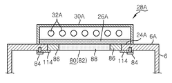
도시하는 바와 같이, 이 열처리 장치(4)는 알루미늄 합금 등에 의해 통체형상으로 성형된 처리용기(6)를 갖고 있다. 이 처리용기(6)의 측벽에는 이 중에 피처리체로서의 반도체 웨이퍼 W를 반출 반입하기 위한 개구(8)가 마련되고, 이 개구(8)에는 기밀하게 개폐 가능하게 이루어진 게이트밸브(10)가 마련된다. 또한, 이 처리용기(6)의 측벽에는 이 처리용기(6)내에 어닐 등의 열처리시에 필요한 소정의 가스, 예를 들면, N2나 O2 가스 등을 공급하기 위한 가스 공급 수단(12)이 마련되어 있다. As shown, this
여기서는 이 가스 공급 수단(12)으로서, 예를 들면, 석영으로 이루어지는 가스 공급 노즐(12A)이 처리용기(6)의 측벽을 관통시켜 마련되어 있고, 도시하지 않은 매스플로 컨트롤러(Mass Flow Controller (MFC) 등의 유량 제어기에 의해 유량 제어하면서 상기 가스를 공급할 수 있도록 되어 있다. 또한, 이 가스 공급 노즐(12A) 대신에, 예를 들면, 석영제의 샤워헤드 구조 등을 이용해도 좋다. Here, as this gas supply means 12, for example, a
또한, 이 처리용기(6)의 바닥부에는 배기구(14)가 마련되어 있다. 이 배기구(14)에는 배기 통로(16)에 압력 조정 밸브(17) 및 진공 펌프 등의 배기펌프(18)를 순차 개재해서 이루어지는 배기 수단(20)이 접속되어 있고, 상기 처리용기(6)내의 분위기를 배기, 예를 들면, 진공 배기할 수 있도록 되어 있다. 또한, 처리용기(6)내는 처리형태에 따라 대기압에서 고진공 상태까지 각종 압력 제어가 가능하다. Moreover, the
또한, 상기 처리용기(6)는 천장부(6A)를 갖고 있으며, 이 천장부(6A)에는 대구경의 개구부(22A)가 형성되어 있다. 이 개구부(22A)에는 O링 등의 시일 부재(24A)를 거쳐서, 예를 들면, 투명 석영판으로 이루어지는 제 1 조사창(26A)이 기밀하게 부착 고정되어 있다. 그리고, 상기 제 1 조사창(26A)의 외측에는 제 1 가열 수단(28A)이 마련되어 있다. 이 제 1 가열 수단(28A)은 내면이 반사면으로 이루어진 램프 하우스(30A)를 갖고 있다. 이 램프 하우스(30A)내에는 직관(Straight Tube)형상으로 이루어진, 예를 들면, 할로겐 램프로 이루어지는 가열 램프(32A)가 복수개 병렬로 배치되어 있고, 이들 가열 램프(32A)로부터의 방사광(열선)으로 반도체 웨이퍼 W를 가열할 수 있도록 되어 있다. Moreover, the said
또한, 상기 할로겐 램프로서 구형의 램프를 이용해도 좋다. 또한, 여기서는 처리용기(6)의 바닥부(6B)에는, 예를 들면, 파이로 센서(Pyrometer)(방사 온도계)로 이루어지는 온도 측정기(34)가 마련되어 있다. 온도 측정기(34)의 측정값이, 예를 들면, 마이크로컴퓨터 등으로 이루어지는 온도 제어부(36)에 입력되고, 상기 측정값에 의거하여 상기 제 1 가열 수단(28A)으로의 투입 전력을 제어해서 반도체 웨이퍼를 소정의 온도로 제어할 수 있도록 되어 있다. 이 경우, 제 1 가열 수단(28A)을, 예를 들면, 내주 존(Zone)과 외주 존으로 동심원형상으로 구획해서 각 존마다 개별적으로 온도 제어할 수 있도록 해도 좋다. In addition, you may use a spherical lamp as said halogen lamp. In addition, here, the
그리고, 이 처리용기(6)내에는 상기 반도체 웨이퍼 W를 지지하기 위한 지지 수단(38)이 마련되어 있다. 또한, 여기서는 이 지지 수단(38)은 반도체 웨이퍼 W의 반출 반입시에 반도체 웨이퍼 W를 승강시키는 승강 기구(40)의 일부를 겸하고 있다. In the
구체적으로, 상기 지지 수단(38)은, 예를 들면, 석영(Quartz)로 이루어지는 대구경의 원형 링형상의 승강판(42)을 갖고 있다. 이 승강판(42)은 마찬가지로 석영으로 이루어지는 대구경의 원형 링형상의 탑재판(44)상에 탑재되어 있다. 이 승강판(42)을 지지하는 링형상의 탑재판(44)은 처리용기(6)의 측벽에 고정되어 있는 것은 아니고, 여기서는 회전 기구(46)에 의해서 회전 가능하게 이루어져 있다. 구체적으로는 이 회전 기구(46)는 처리용기(6)의 측벽에 축받이(48)를 거쳐서 회전 자유롭게 지지된 복수의 회전 롤러(50)를 갖고 있다. 이 회전 롤러(50)는 처리용기(6)의 둘레방향을 따라 균등한 간격을 두고 적어도 3개(도시 예에서는 2개 나타냄) 마련되어 있다. Specifically, the support means 38 has, for example, a large-diameter circular ring-shaped
상기 축받이(48)는 처리용기(6)내의 기밀성을 유지하면서 상기 회전 롤러(50)의 회전을 허용하기 위해, 예를 들면, 자성유체에 의해 시일되어 있다. 상기 각 회전 롤러(50)는, 예를 들면, 석영으로 이루어지고, 또한, 예를 들면, 절두(Truncated) 원추대형상으로 성형되어 있다. 또한, 각 회전 롤러(50)의 상면측에 상기 탑재판(44)이 탑재되어 지지되어 있고, 이 회전 롤러(50)를 회전 구동하는 것에 의해, 상기 탑재판(44)을 그 둘레방향으로 회전할 수 있도록 되어 있다. 이 회전 구동을 얻기 위해, 상기 3개의 회전 롤러(50) 중의 1개에 구동 모터(52)를 접속하고 있다. The
또, 상기 탑재판(44)의 외측 코너부에는 그 둘레방향을 따라, 예를 들면, SiC로 이루어지는 단단한 받이부재(54)가 마련되어 있고, 이 받이부재(54)에 상기 회전 롤러(50)를 직접적으로 접촉시키고 있다. 이 받이부재(54)를 마련하는 것에 의해, 여기에 파티클이 발생하는 것을 방지하도록 되어 있다. The outer corner portion of the mounting
또한, 상기 탑재판(44)의 일부에는 위치결정 구멍(56)이 형성되어 있으며, 이 위치결정 구멍(56)의 상하에, 예를 들면, 레이저광을 발생하는 발광 기(58)와, 레이저광을 수광하는 수광기(60)를 마련하고 있다. 그리고, 이 위치결정 구멍(56)을 통과하는 레이저광을 검출하는 것에 의해, 상기 탑재판(44)의 홈 포지션을 검출해서 회전방향의 위치를 인식할 수 있도록 되어 있다. 또한, 이 탑재판(44)을 처리용기(6)의 측벽측에 고정시켜 회전시키지 않도록 해도 좋다. In addition, a
그리고, 상기 링형상의 승강판(42)으로부터는 그 중앙방향을 향해 복수개, 예를 들면, 석영으로 이루어지는 3개(도시 예에서는 2개만 나타냄)의 지 아암(62)이 연장시켜 마련되어 있다. 이 지지 아암(62)은 승강판(42)의 둘레방향을 따라 등간격으로 배치되어 있다. 그리고, 상기 각 지지암(62)의 선단부에는, 예를 들면, 석영으로 이루어지는 지지핀(64)이 마련되어 있고, 각 지지핀(64)의 상단을 상기 반도체 웨이퍼 W의 이면의 주변부에 접촉시켜, 이 반도체 웨이퍼 W를 지지하도록 되어 있다. From the ring-shaped
그리고, 상기 승강판(42)을 승강시키기 위해, 승강 기구(40)의 일부로서 처리용기(6)의 바닥부(6B)에는 승강 액추에이터(66)가 마련되어 있다. 이 승강 액추에이터(66)는 상기 바닥부(6B)의 둘레방향을 따라, 예를 들면, 3개(도시 예에서는 2개만 나타냄) 마련되어 있다. 각 승강 액추에이터(66)에는 용기 바닥부(6B)의 관통구멍(68)을 헐겁게 끼운 상태에서 삽입통과된 승강 로드(70)가 마련되어 있다. In order to elevate the elevating
또한, 상기 탑재판(44)에도 승강 로드(70)를 통과시키기 위한 삽입통과 구멍(72)이 형성되어 있다. 이 삽입통과 구멍(72)에 상기 승강 로드(70)의 상단부를 삽입통과시켜 상기 승강판(42)을 위쪽으로 밀어 올릴 수 있도록 되어 있다. 이 승강 액추에이터(66)와 상기 지지 수단(38)에 의해, 승강 기구(40)가 형성되어 있다. 또, 상기 승강 로드(70)의 바닥부 관통부에는 신축 가능하게 이루어진 금속 벨로우(Bellow)(74)가 개재되어 있고, 상기 처리용기(6)내의 기밀성을 유지하면서 상기 승강 로드(70)의 승강 이동을 허용할 수 있도록 되어 있다. In addition, the mounting
그리고, 이 처리용기(6)내에서, 상기 지지 수단(38)과 상기 제 1 조사창(26A)의 사이에, 본 발명의 특징으로 하는 막 방착 부재(Anti-adhesion member)(80)가 마련된다. 구체적으로는, 이 막 방착 부재(80)는 전체가, 예를 들면, 원형의 내열성 및 내부식성이 큰 석영 유리판(82)으로 이루어지고, 제 1 조사창(26A)의 전체면을 덮는 크기로 설정되어 있다. 환언하면, 막 방착 부재(80)는 반도체 웨이퍼 W의 전체면을 덮도록 이 반도체 웨이퍼 W와 동등하거나, 혹은 이보다도 큰 직경으로 설정되어 있다. In this
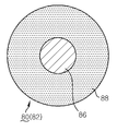
그리고, 막 방착 부재(80)는 상기 천장부(6A)에, 여기에 형성되어 있는 개구부(22A)를 덮도록 볼트(84)에 의해 착탈 가능하게 부착 고정되어 있다. 이것에 의해, 이 석영 유리판(82)에 어느 정도의 부착물이 퇴적했을 때에 이 석영 유리판(82)을 교환할 수 있도록 되어 있다. 상기 볼트(84)로서는 금속오염 등이 생기지 않는 바와 같은 재료, 예를 들면, 알루미늄 합금이나 세라믹재를 이용한다. 그리고, 이 석영 유리판(82)은 그 일부에 상기 제 1 가열 수단(28A)으로부터의 조사광(열선)의 일부 혹은 전부를 차단하기 위한 차광부(86)가 형성되어 있다. The
도 2a에도 나타내는 바와 같이, 여기서는 반도체 웨이퍼 W의 주변부(에지부)에 도달하는 열량을 억제하기 위해, 상기 차광부(86)는 상기 석영 유리판(82)의 주변부에 링형상으로 형성되어 있다(도 2a와 2b에 있어서 사선으로 나타내는 영역). 그리고, 상기 차광부(86) 이외의 영역, 즉, 여기서는 중앙부측의 투과 영역(88)은 열선에 대해 투명한 상태로 되어 있고, 여기를 통과하는 상기 열선을 손실시키는 일 없이 투과시켜 반도체 웨이퍼 W를 가열할 수 있도록 되어 있다. As also shown in FIG. 2A, in order to suppress the amount of heat which reaches the peripheral part (edge part) of the semiconductor wafer W here, the said
상술한 바와 같이, 상기 차광부(86)는 여기를 통과하는 열선량을 억제하기 위해 불투명 유리 상태로 이루어져 있다. 이 경우, 불투명 유리 상태는 조사광이 통과하는 것을 완전히 차단하는 상태로부터 조사 광의 일부를 통과시킬 수 있는 소위 반투명 상태의 경우도 포함하고, 그 투과도는 반도체 웨이퍼 W상에 형성되어 있는 어닐 대상으로 되는 박막의 어닐에 의한 막두께 특성 등에 의거하여 결정된다. 구체적으로는, 이 차광부(86)에서는 불투명 유리 상태, 젖빛 유리 상태, 광택이 없는 유리 상태, 기포가 내포된 발포 유리 상태, 혹은 유백색의 탁한 유리 상태로 되어 있고, 바람직하게는 이 차광부(86)에서는 조사광을 난반사시키는 바와 같은 상태로 설정해 두는 것이 좋다. 또한, 상기 차광부(86)로서는, 예를 들면, 산화마그네슘을 투명 유리상에 차광재로서 코팅하도록 구성해도 좋다. As described above, the
이것에 의해, 반도체 웨이퍼 W의 중심부에는 대량의 열선이 도달하고, 주변부에는 소량의 열선밖에 도달하지 않도록 제어할 수 있도록 되어 있다. 그리고, 이 석영 유리판(82)에는 상기 제 1 조사창(26A)의 하면과 석영 유리판(82)의 상면의 사이에서 구획되는 공간(90)내의 압력 조정(압력 경감)을 하기 위한 압력조정 연통로(92)가 형성되어 있다(도 1 참조). 이것에 의해, 처리용기(6)내를 승압 혹은 강압시켜도, 상기 석영 유리판(82)에 압력차에 의한 힘이 작용하지 않도록 하여, 파손을 방지할 수 있도록 되어 있다. As a result, a large amount of hot wire reaches the center portion of the semiconductor wafer W and only a small amount of the hot wire reaches the peripheral portion. And this
상기 압력 조정 연통로(92)는 여기서는 미소한 관통구멍(92A)에 의해 형성되어 있다. 이 경우, 관통구멍(92A) 대신에, 석영 유리판(82)의 상면의 주변부에, 반경방향으로 연장하는 미소한 연통 홈 등을 형성하도록 해도 좋다. 또한, 상기 석영 유리판(82)을 천장부(6A)에 부착했지만, 이것을 처리용기(6)의 측벽으로부터 지지시키도록 해도 좋다. The pressure
또한, 도 2a에 나타내는 경우에는 석영 유리판(82)의 중앙부가 투과 영역(88)으로 되고, 주변부가 차광부(86)로 되어 있지만, 이와는 반대로, 도 2b에 나타내는 경우에는 석영 유리판(82)의 중앙부가 차광부(86)로 되고, 주변부가 투과 영역(88)으로 되어 있다. 이것에 의해, 어닐 대상의 박막의 특성에 대응시켜 상기 도 2a와 2b에 나타내는 이종의 막 방착 부재(80)를 교환해서 이용할 수 있도록 되어 있다. In addition, when shown to FIG. 2A, the center part of the
그리고, 이 장치 전체의 동작, 예를 들면, 반도체 웨이퍼 온도, 용기내의 압력, 각 가스의 공급량 등의 각 제어는 컴퓨터로 이루어지는 장치 제어부(96)에 의해서 실행된다. 그리고, 이 제어에 필요한 컴퓨터에 판독 가능한 프로그램은 기억 매체(98)에 미리 기억되어 있다. 이 기억 매체(98)는, 예를 들면, 플렉시블 디스크, CD(Compact Disc), CD-ROM, 하드 디스크, 플래시 메모리, 혹은 DVD 등으로 이루어진다. The operation of the entire apparatus, for example, the semiconductor wafer temperature, the pressure in the vessel, the supply amount of each gas, and the like are executed by the
다음으로, 이상과 같이 구성된 열처리 장치(4)의 동작에 대해 설명한다. 우선, 이 처리용기(6)내에 반도체 웨이퍼 W를 반입하는 경우에는 개방된 게이트밸브(10)로부터 개구(8)를 거쳐서 도시하지 않은 반송 아암으로 반도체 웨이퍼 W를 처리용기(6)내에 반입한다. 이 상태에서 승강 기구(40)의 승강 액추에이터(66)를 구동해서 승강 로드(70)를 위쪽으로 연장시키고, 이것에 의해, 지지 수단(38)의 승강판(42)을 위쪽으로 밀어 올려 지지 핀(64)을 상승시킨다. Next, operation | movement of the
이것에 의해, 반송 아암(도시하지 않음)에 의해서 처리용기(6)내에 반입되어 있는 반도체 웨이퍼 W가 아래쪽으로부터 상승해 오는 지지 핀(64)에 의해 밀어 올려지고, 이것에 의해 반송 아암으로부터 지지 핀(64)에 반도체 웨이퍼 W가 수수되어 유지된다. Thereby, the semiconductor wafer W carried in the
다음으로, 반송 아암을 처리용기(6)내로부터 빼내어, 상술한 바와 같이, 반도체 웨이퍼 W를 지지 핀(64)으로 유지한 상태에서, 상기 승강 로드(70)를 강하시킨다. 이것에 의해, 도 1에 나타내는 바와 같이, 승강판(42)은 탑재판(44)상에 탑재되게 된다. 그리고, 게이트밸브(10)를 닫아 처리용기(6)내를 밀폐하고, 가스 공급 수단(12)으로부터 필요한 가스, 예를 들면, N2 및 O2 가스를 각각 유량 제어하면서 처리용기(6)내에 공급한다. 또한, 배기 수단(20)을 구동해서 처리용기(6)내를 소정의 압력 분위기로 유지한다. Next, the transfer arm is removed from the inside of the
그리고, 회전 기구(46)의 구동 모터(52)를 구동시키는 것에 의해 회전 롤러(50)를 회전하고, 이것에 의해 탑재판(44) 및 승강판(42)을 둘레방향으로 회전시킴으로써, 반도체 웨이퍼 W를 동일 평면내에서 회전시킨다. 그리고, 제 1 가열 수단(28A)의 각 가열 램프(32A)를 점등해서 반도체 웨이퍼 W의 온도를 소정의 온도, 예를 들면, 1050℃ 정도로 유지하면서 열처리, 예를 들면, 어닐 처리를 하게 된다. Then, the rotating
이 어닐 처리를 실행하고 있는 동안에는 상기 반도체 웨이퍼 W의 온도는 용기 바닥부(6B)에 마련한, 예를 들면, 방사 온도계로 이루어지는 온도 측정기(34)에 의해 측정된다. 이 온도측정기(34)에 의한 측정값에 의거하여 상기 온도 제어부(36)는 상기 제 1 가열 수단(28A)으로부터의 조사광을 피드백 제어한다. 이것에 의해, 반도체 웨이퍼 W는 미리 설정된 소정의 온도로 유지되게 된다. During this annealing process, the temperature of the semiconductor wafer W is measured by a
상기 반도체 웨이퍼 W의 표면에는 이전 공정에서 어닐 처리가 대상으로 되는 박막이 미리 형성되어 있고, 이 어닐 처리에 의해 상기 박막이 가열되어 어닐 처리에 의해 막질의 개질 등이 실행되게 된다. On the surface of the semiconductor wafer W, a thin film to be annealed in the previous step is formed in advance, and the thin film is heated by the annealing treatment, and the film quality is modified by the annealing treatment.
상기 박막은, 예를 들면, 실리콘 산화막(SiO2)이거나, 실리콘 질화막(SiN)이거나, 각종 박막이 어닐 처리가 대상으로 된다. 여기서, 어닐 처리의 프로세스 조건으로서는 어닐 대상으로 되는 박막의 막종에도 따르지만, 반도체 웨이퍼 온도는 700∼1050℃ 정도의 범위내, 압력은 0.1Torr (13.3Pa) ∼ 760Torr (1018Pa) 정도의 범위내, N2 가스는 500∼10000sccm의 범위내, O2 가스는 0∼100sccm의 범위내이다. The thin film is, for example, a silicon oxide film (SiO 2 ), a silicon nitride film (SiN), or various thin films are subjected to annealing treatment. Here, the process conditions of the annealing process also depend on the film type of the thin film to be annealed, but the semiconductor wafer temperature is in the range of about 700 to 1050 ° C, and the pressure is in the range of about 0.1 Torr (13.3 Pa) to 760 Torr (1018 Pa). 2 gas is in the range of 500 to 10000 sccm, and O 2 gas is in the range of 0 to 100 sccm.
여기서, 상기 박막의 형성된 반도체 웨이퍼 W가 어닐 처리 중에, 예를 들면, 1050℃ 정도로 가열되면, 이 박막으로부터, 예를 들면, 박막이 분해된 물질이 발생하거나, 처리용기(6)내의 각 부재로부터 어떠한 물질이 발생한다. 이 경우, 종래의 열처리 장치에 있어서는 이 발생한 물질이 화살표 ‘99’로 나타내는 바와 같이 상승해서 조사창에 부착 퇴적해서 흐릿함이 발생하고, 메인터넌스 유지에 장시간을 요할 뿐 아니라, 메인터넌스 비용도 높게 되고 있다. Here, when the semiconductor wafer W formed of the thin film is heated to, for example, about 1050 ° C., during the annealing process, a substance from which the thin film is decomposed, for example, is generated, or from each member in the
이에 대해, 본 발명의 경우에는 이 반도체 웨이퍼 W의 위쪽, 즉, 천장부(6A)에 마련한 제 1 조사창(26A)의 아래쪽에는 교환 작업이 용이한, 예를 들면, 석영 유리판(82)으로 이루어지는 막 방착 부재(80)가 마련되어 있다. 그 결과, 상기 박막 등으로부터 발생한 물질은 상기 석영 유리판(82)의 하면에 부착 퇴적하게 되고, 제 1 조사창(26A)에 부착 퇴적하는 것을 방지할 수 있다. On the other hand, in the case of this invention, the upper part of this semiconductor wafer W, ie, the lower part of the
따라서, 어느 정도의 개수의 반도체 웨이퍼 W를 어닐 처리하면, 상기 석영 유리판(82)을 새로운 것으로 교환한다. 이 경우의 메인터넌스 작업은 이 석영 유리판(82)을 단지 교환하는 것뿐이므로, 매우 신속하고 또한 용이하게 실행할 수 있다. 따라서, 장치의 가동률이 저하하는 것을 방지할 수 있다. Therefore, when a certain number of semiconductor wafers W are annealed, the
또한, 종래의 열처리 장치에서는 반도체 웨이퍼 W의 표면에 형성되어 있는 막종에 따라서는 상기한 어닐 처리 후(열처리 후)에, 반도체 웨이퍼 W면상의 박막의 주변부가 중앙부보다도 두꺼워지거나, 혹은 반대로, 주변부가 중앙부보다도 얇아져, 막두께의 면내 균일성이 대폭 저하하는 경우가 있었다. In the conventional heat treatment apparatus, depending on the film type formed on the surface of the semiconductor wafer W, after the annealing treatment (after heat treatment), the peripheral portion of the thin film on the semiconductor wafer W surface becomes thicker than the center portion, or vice versa. It became thinner than a center part, and the in-plane uniformity of film thickness might fall significantly.
이에 대해, 본 발명에서는 막 방착 부재(80)인 석영 유리판(82)의 일부에, 제 1 가열 수단(28A)으로부터의 열선(조사광)의 일부 혹은 전부를 차단하기 위한 차광부(86)를 마련해서 그 부분의 투과율이나 복사율을 저하시켜 반도체 웨이퍼 W의 표면의 대응하는 부분에 들어가는 열량을 억제하도록 했으므로, 그 부분의 막두께의 증가를 적게 할 수 있고, 그 결과, 막두께의 면내 균일성을 높게 유지할 수 있다. In contrast, in the present invention, a part of the
구체적으로는, 도 3a에 나타내는 바와 같이, 종래의 경향으로서, 반도체 웨이퍼 W상에 형성한 박막(110)이, 어닐 처리 후에 있어서 중앙부가 얇아지고, 주변부가 두꺼워지는 바와 같은 특성을 갖고 있는 박막을 어닐 처리하는 경우에는 도 2a에 나타낸 바와 같이, 중앙부에 투과 영역(88)이 있고, 주변부에 링형상의 차광부(86)를 갖는 막 방착 부재(80)를 이용해서 어닐 처리를 실행한다. 이것에 의해, 박막(110)의 주변부에 입사하는 열량(조사량)이 감소해서 이 주변부의 막두께의 증가가 억제되므로, 어닐 처리 후에 있어서의 막두께의 면내 균일성을 향상시킬 수 있다. Specifically, as shown in FIG. 3A, as a conventional trend, the
또 반대로, 도 3b에 나타내는 바와 같이, 종래의 경향으로서, 반도체 웨이퍼 W상에 형성한 박막(110)이, 어닐 처리 후에 있어서 중앙부가 두꺼워지고, 주변부가 얇아지는 바와 같은 특성을 갖고 있는 박막을 어닐 처리하는 경우에는 도 2b에 나타낸 바와 같이, 주변부에 투과 영역(88)이 있고, 중앙부에 링형상의 차광부(86)를 갖는 막 방착 부재(80)를 이용해서 어닐 처리를 실행한다. 이것에 의해, 박막(110)의 중앙부에 입사하는 열량(조사량)이 감소하여 이 중앙부의 막두께의 증가가 억제되고, 어닐 처리 후에 있어서의 막두께의 면내 균일성을 향상시킬 수 있다. On the contrary, as shown in FIG. 3B, as a conventional trend, the
또한, 어닐 처리를 실행하는 과정에서, 처리용기(6)내의 압력을 크게 변화시키는 경우가 있지만, 이 경우, 제 1 조사창(26A)과 막 방착 부재(80)의 사이에 구획 형성되는 공간(90)내의 압력은 상기 막 방착 부재(80)에 형성한 압력 조정 연통로(92)를 통해 가스가 통과함으로써 반도체 웨이퍼 W가 탑재되어 있는 측의 처리용기(6)내의 압력과 동일하게 된다. 그 결과, 막 방착 부재(80)에 압력차에 의한 힘이 작용하는 일이 없어지며, 막 방착 부재(80)의 파손을 방지할 수 있다. In the process of carrying out the annealing process, the pressure in the
이와 같이, 본 발명 장치의 제 1 실시예에 의하면, 막 방착 부재(80)에 국부적으로 열선의 투과를 일부 혹은 전부를 차단하는 차광부(86)를 마련하는 것에 의해, 조사창(제 1 조사창(26A))에 흐릿함이 발생하는 것을 방지하면서 열처리 후에 있어서의 박막의 막두께의 면내 균일성을 높게 유지할 수 있다. As described above, according to the first embodiment of the apparatus of the present invention, by providing the
(제 2 실시예) (Second embodiment)
다음으로, 본 발명의 제 2 실시예에 대해 설명한다. Next, a second embodiment of the present invention will be described.
이 제 2 실시예는 상술한 일본 특허공개 제2006-5177호 공보(특허문헌 3)에서 개시한 바와 같은 미러링 제어를 실행하는 열처리 장치에 본 발명을 적용하고 있다. 도 4는 본 발명에 관한 열처리 장치의 제 2 실시예를 나타내는 단면도이다. 또한, 도 1 내지 도 3b에 나타내는 구성 부분과 동일 구성 부분에 대해서는 동일 참조 부호를 붙이고 그 설명을 생략한다. This second embodiment applies the present invention to a heat treatment apparatus for performing mirroring control as disclosed in Japanese Patent Laid-Open No. 2006-5177 (Patent Document 3) described above. 4 is a cross-sectional view showing the second embodiment of the heat treatment apparatus according to the present invention. In addition, the same code | symbol is attached | subjected about the component same as the component shown in FIGS. 1-3, and the description is abbreviate | omitted.
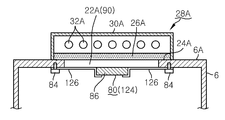
이 제 2 실시예에서는 반도체 웨이퍼 W의 아래쪽으로서, 이 반도체 웨이퍼 W와 대향시키도록 해서 모의 피처리체로서의 모의 웨이퍼(102)가 지지되어 있다. 또한, 그 아래쪽에, 즉, 처리용기(6)의 바닥부(6B)에 상기 모의 웨이퍼(102)를 가열하는 제 2 가열 수단(28B)이 마련되어 있다. 구체적으로는 상기 처리용기(6)의 바닥부(6B)에는 대구경의 개구부(22B)가 형성되어 있고, 이 개구부(22B)에는 O링 등의 시일 부재(24B)를 거쳐서, 예를 들면, 투명 석영판으로 이루어지는 제 2 조사창(26B)이 기밀하게 부착 고정되어 있다. In this second embodiment, a
그리고, 상기 제 2 조사창(26B)의 외측에는 제 2 가열 수단(28B)이 마련되어 있다. 이 제 2 가열 수단(28B)은 내면이 반사면으로 이루어진 램프 하우스(30B)를 갖고 있으며, 이 램프 하우스(30B)내에는 직관(Straight tube)형상으로 이루어진, 예를 들면, 할로겐 램프로 이루어지는 가열램프(32B)가 복수개 병렬로 배치되어 있고, 이들 가열 램프(32B)로부터의 방사광(열선)으로 상기 모의 웨이퍼(102)를 가열할 수 있도록 되어 있다. And the 2nd heating means 28B is provided in the outer side of the said
또한, 상기 할로겐 램프로서 구형의 램프를 이용해도 좋다. 또한, 여기서는 제 2 가열 수단(28B)의 램프 하우스(30B)에는, 예를 들면, 파이로 센서{}(방사 온도계)로 이루어지는 온도 측정기(34)가 마련되어 있다. 이 온도 측정기(34)에는, 예를 들면, 마이크로컴퓨터 등으로 이루어지는 온도 제어부(36)가 접속되어 있다. 온도 측정기(34)의 측정값은 온도 제어부(36)에 입력되고, 상기 측정값에 의거하여 상기 제 2 가열 수단(28B)으로의 투입 전력을 제어해서 반도체 웨이퍼를 소정의 온도로 제어할 수 있도록 되어 있다. 이 경우, 제 2 가열 수단(28B)을, 예를 들면, 내주 존(Zone)과 외주 존으로 동심원형상으로 구획해서 각 존마다 개별적으로 온도 제어할 수 있도록 해도 좋다. In addition, you may use a spherical lamp as said halogen lamp. In addition, here, the
즉, 여기서는 상기 온도 측정기(34)로 상기 모의 웨이퍼(102)의 이면의 온도를 측정하고, 이 측정값에 의거하여 상기 온도 제어부(36)는 제 1 및 제 2 가열 수단(28A, 28B)의 양쪽을 제어하도록 하고 있다. 이 경우, 제 1 및 제 2 가열 수단(28A, 28B)으로부터는 서로 동일한 열량의 조사광을 방사하도록 제어, 즉, 미러링 제어를 실행하도록 되어 있다. 따라서, 상기 제 1 및 제 2 가열 수단(28A, 28B)의 각 가열 램프(32A, 32B)의 와트 수는 동일하게 설정되고, 또한 반도체 웨이퍼 W와 제 2 조사창(26B) 사이의 거리 L2와 모의 웨이퍼(102)와 제 1 조사창(26A) 사이의 거리 L1은 동일 값으로 설정되어 있고, 서로의 열적 조건이 동일하게 되도록 설정되어 있다. That is, here, the
이 경우, 상기 모의 웨이퍼(102)를 지지하기 위해, 상기 탑재판(44)에는 그 중심방향에 수평으로 연장하는, 예를 들면, 석영으로 이루어지는 복수개의 지지 로드(104)가 마련된다. 이 지지 로드(104)는 탑재판(44)의 둘레방향을 따라 등간격으로, 예를 들면, 3개(도시 예에서는 2개만 나타냄) 마련되어 있고, 그 선단부는 위쪽으로 L자형상으로 굴곡되어 있다. 그리고, 각 지지 로드(104)의 선단부에서 원판형상의 모의 웨이퍼(102)를 수평으로 지지하고 있다. 이 모의 웨이퍼(102)는 반도체 웨이퍼 W와 동일 형태로 되도록 형성되어 있다. In this case, in order to support the
구체적으로는 이 모의 웨이퍼(102)로서는 반도체 웨이퍼 W와 동일한 직경 및 두께의, 예를 들면, 실리콘 웨이퍼를 이용할 수 있다. 또, 표면에 아무것도 형성되어 있지 않은 실리콘 웨이퍼(베어(bare) 웨이퍼)에 있어서는 적외선 영역의 파장에 대해 투과성이 있기 때문에, 이 영역의 파장을 흡수해서 반도체 웨이퍼 W와 동일하게 가열되도록, 모의 웨이퍼(102)의 표면에는 SiN이나 SiO2 등으로 이루어지는 코팅막이 형성되어 있다. Specifically, for example, a silicon wafer having the same diameter and thickness as that of the semiconductor wafer W can be used as the
그리고, 상기 모의 웨이퍼(102)상에, 예를 들면 3개(도 4 중에서는 2개만 나타냄)의 지지 핀 부재(106)가 둘레방향을 따라 등간격으로 용착(溶着) 등에 의해서 부착되어 있다. 그리고, 이 각 지지 핀 부재(106)의 상단부에서 반도체 웨이퍼 W를 지지하도록 되어 있다. 이것에 의해, 모의 웨이퍼(102)는 반도체 웨이퍼 W에 대해 평행하게 배열되게 된다. On the
그리고, 상기 승강판(42)으로부터 연장하는 각 지지암(62)의 선단에는 위쪽으로 기립시킨 리프트 핀(108)이 부착되어 있다. 이 리프트 핀(108)은 상기 모의 웨이퍼(102)에 형성한 핀 구멍(110)내를 위쪽으로 관통해서 마련되어 있고, 이 리프트 핀(108)을 승강시키는 것에 의해서, 반도체 웨이퍼 W를 위쪽으로 밀어 올려 반도체 웨이퍼 W의 수수가 가능하도록 되어 있다. A
따라서, 이 리프트 핀(108)은 반도체 웨이퍼를 들어 올리는 승강 기구(40)의 일부로서 구성되어 있다. 그리고, 이 경우에도, 상기 제 1 조사창(26A)의 아래쪽에 본 발명의 특징으로 하는 상기의 막 방착 부재(80)가 마련되어 있다. 이 막 방착 부재(80)의 구성 및 변형예는 상기의 도 1 내지 도 3을 참조해서 설명한 바와 같다. Therefore, this
이와 같이 구성된 제 2 실시예에 있어서는 반도체 웨이퍼 W의 어닐 처리시의 온도 제어로서, 소위 미러링 제어가 실행된다. 즉, 제 2 가열 수단(28B)에 의해서 모의 웨이퍼(102)가 원하는 온도로 되도록 온도 측정기(34)로 모의 웨이퍼(102)의 온도를 모니터하면서 피드백으로 온도 제어한다. 이 때, 천장부의 제 1 가열 수단(28A)과 바닥부의 제 2 가열 수단(28B)에 투입되는 전력은 각각 완전히 동일하게 되도록, 소위 미러링 제어된다. 이것에 의해, 반도체 웨이퍼 W의 온도를 모의 웨이퍼(102)의 온도와 동일하게 되도록 제어할 수 있고, 결과적으로 반도체 웨이퍼 W의 온도를 원하는 온도로 유지할 수 있게 된다. In the second embodiment configured as described above, so-called mirroring control is executed as temperature control at the time of annealing the semiconductor wafer W. As shown in FIG. That is, the temperature is controlled by the feedback while the
또한, 실제적으로는 반도체 웨이퍼 W와 모의 웨이퍼(102)의 광흡수율의 차로부터, 상하의 제 1 및 제 2 가열 수단(28A, 28B)에 투입되는 전력은 완전히 동일하지는 않고, 이들 사이에는 오프셋적인 값의 어긋남은 존재한다. 이와 같이 미러링 제어를 실행하는 이유는 모의 웨이퍼(102)의 이면은 광학적으로 안정되어 있는데 반해, 반도체 웨이퍼 W로서는 각종 처리가 이전공정에서 실행된 것이 반입되므로, 광학적으로 항상 일정한 것이 반입되어 온다고는 한정할 수 없어, 이와 같은 반도체 웨이퍼 W의 온도를 방사 온도계로 이루어지는 온도 측정기(34)로 정밀도 좋게 검출하는 것은 곤란하기 때문이다. Further, in practice, the power input to the first and second heating means 28A, 28B on the upper and lower sides from the difference in the light absorption rate between the semiconductor wafer W and the
그리고, 이 제 2 실시예의 경우에도, 막 방착 부재(80)를 마련하고 있기 때문에, 상기의 제 1 실시예와 대략 마찬가지의 작용 효과를 발휘할 수 있다. 즉, 막 방착 부재(80)에 국부적으로 열선의 투과를 일부 혹은 전부를 차단하는 차광부(86)를 마련하는 것에 의해, 조사창(제 1 조사창(26A))에 흐릿함이 발생하는 것을 방지하면서 열처리 후에 있어서의 박막의 막두께의 면내 균일성을 높게 유지할 수 있다. Also in the case of this second embodiment, since the
(제 3 실시예) (Third embodiment)
다음으로, 본 발명의 제 3 실시예에 대해 설명한다. Next, a third embodiment of the present invention will be described.
상기의 제 1 및 제 2 실시예에서는 처리용기(6)의 천장부(6A)에 막 방착 부재(80)를 부착할 때에, 이것과 제 1 조사창(26A)의 사이에 공간(90)이 형성되어 있었지만, 이것에 한정되지 않고, 양자를 밀착시켜 마련하도록 해도 좋다. 도 5는 이와 같은 본 발명에 관한 열처리 장치의 제 3 실시예의 주요부를 나타내는 확대 단면도이고, 다른 부분은 도 1 내지 도 4에 나타내는 바와 같은 구성으로 이루어져 있다. 여기서는 도 1 내지 도 4에 나타내는 구성 부분과 동일 구성 부분에 대해서는 동일 참조 부호가 붙어 있다. In the above first and second embodiments, the
도 5에 나타내는 바와 같이, 이 제 3 실시예에서는 막 방착 부재(80)는 상기 제 1 조사창(26A)의 하면에 밀착시켜 부착되어 있고, 이 막 방착 부재(80)는 볼트(84)로 체결된 누름판(114)에 의해 착탈 가능하게 고정되어 있다. 이 경우에는 상기 공간(90)이 형성되지 않으므로, 이 막 방착 부재(80)가 압력차에 의해 파손되는 것을 방지하는 압력 조정 연통로(92)(도 1 참조)를 마련할 필요가 없다. As shown in FIG. 5, in this 3rd Example, the membrane | film |
이 제 3 실시예에서는 상기의 제 1 및 제 2 실시예에서 설명한 기술을 모두 적용할 수 있고, 또한 제 1 및 제 2 실시예에서 설명한 바와 같은 작용 효과를 발휘할 수 있다. In this third embodiment, all of the techniques described in the first and second embodiments described above can be applied, and the same effects as described in the first and second embodiments can be achieved.
(제 4 및 제 5 실시예) (4th and 5th Example)
다음으로, 본 발명의 제 4 및 제 5 실시예에 대해 설명한다. Next, the fourth and fifth embodiments of the present invention will be described.
상기의 제 1 내지 제 3 실시예에서는 막 방착 부재(80)로서, 제 1 조사창(26A)의 하면의 전체면을 덮는 크기의 원판형상으로 이루어져 있었지만, 이 제 4 및 제 5 실시예에서는 반도체 웨이퍼 W의 표면의 일부에 대응하는 크기로 설정되어 있다. 구체적으로, 제 4 실시예에서는 상기 막 방착 부재(80)는 반도체 웨이퍼 W와 대략 동등한 직경이기는 하지만, 원형 링형상으로 형성되고, 제 5 실시예에서는 반도체 웨이퍼 W보다도 직경이 훨씬 작은 원판형상으로 이루어져 있다. In the first to third embodiments described above, the film-
도 6은 이와 같은 본 발명에 관한 열처리 장치의 제 4 실시예의 주요부를 나타내는 확대 단면도, 도 7a와 7b는 제 4 실시예에서 이용하는 막 방착 부재를 나타내는 평면도, 도 8은 상기한 바와 같은 본 발명에 관한 열처리 장치의 제 5 실시예의 주요부를 나타내는 확대 단면도, 도 9는 제 5 실시예에서 이용하는 막 방착 부재를 나타내는 평면도이다. Fig. 6 is an enlarged cross sectional view showing a main part of a fourth embodiment of the heat treatment apparatus according to the present invention. Figs. 7A and 7B are a plan view showing a film anti-deposition member used in the fourth embodiment, and Fig. 8 is the present invention as described above. An enlarged cross sectional view showing a main part of a fifth embodiment of the heat treatment apparatus according to the present invention, and FIG.
이와 같이, 제 1 조사창(26A)의 하면의 전체에 대해 막 방착 부재를 마련한 제 1∼제 3 실시예와는 달리, 제 1 조사창(26A)의 일부를 덮도록 해서 마련하는 이유는 실험에 의하면, 어닐 대상의 막종이나 어닐 조건에 따라서는 제 1 조사창(26A)의 하면에 있어서 막두께가 균일한 상태에서 전체면에 불필요한 박막이 퇴적하는 것은 아니고, 막두께가 치우쳐서 부착 퇴적하는 경우가 있기 때문이다. 즉, 이 경우에는 불필요한 부착 막의 막두께가, 특히, 두꺼워지는 경향에 있는 영역에 대해 불필요한 부착 막이 퇴적하는 것을 방지하도록 하면, 막 방착 부재(80)를 제 1 조사창(26A)의 전체면에 걸쳐 마련할 필요가 없어지기 때문이다.Thus, unlike the 1st-3rd Example which provided the film | membrane-proof member with respect to the whole lower surface of 26 A of 1st irradiation windows, the reason to arrange | position so that a part of
구체적으로는 도 6 및 도 7에 나타내는 제 4 실시예의 경우에는 막 방착 부재(80)로서는 외경이 제 1 조사창(26A)과 대략 동일한 원형 링형상의 석영 유리판(120)을 이용하고 있다. 이 석영 유리판(120)의 폭 W1은 제 1 조사창(26A)에 퇴적하는 불필요한 부착 막의 막두께 분포에 따라 정해진다. 이 제 4 실시예는 제 1 조사창(26A)의 하면의 주변부에 불필요한 박막이, 특히, 두껍게 퇴적하는 바와 같은 어닐 처리를 실행할 때에 이용한다. Specifically, in the fourth embodiment shown in FIG. 6 and FIG. 7, a circular ring-shaped
이 경우, 도 7a에 나타내는 바와 같이, 이 원형 링형상의 석영 유리판(120)의 전체를 차광부(86)로 해도 좋고, 반대로 도 7b에 나타내는 바와 같이, 이 원형 링형상의 석영 유리판(120)의 전체를 투과 영역(88)으로 해도 좋다. In this case, as shown to FIG. 7A, the whole circular ring shaped
이 제 4 실시예에서는 상기의 제 1 내지 제 3 실시예에서 설명한 기술을 모두 적용할 수 있고, 또한, 제 1 내지 제 3 실시예에서 설명한 바와 같은 작용 효과를 발휘할 수 있다. 이 제 4 실시예에서는 피처리체인 반도체 웨이퍼 W를 지지하는 지지 수단(38)과 조사창(제 1 조사창(26A))의 사이에, 피처리체의 표면의 일부에 대응하는 크기로 설정한 석영 유리판(120)으로 이루어지는 막 방착 부재(80)를 마련하는 것에 의해, 예를 들면, 피처리체로부터 방출되는 물질이 많이 부착되는 영역에 대응시켜 국부적으로 막 방착 부재를 마련할 수 있고, 조사 효율을 높게 유지하면서 조사창에 흐릿함이 발생하는 것을 억제할 수 있다. 단, 이 제 4 실시예의 경우에는 제 1 조사창(26A)의 중심부에 약간 불필요한 막이 퇴적하는 것은 피할 수 없지만, 원형 링형상의 석영 유리판(120)의 중심부에는 아무것도 마련하고 있지 않으므로, 이 부분에 있어서의 열선의 흡수가 없고, 그만큼, 반도체 웨이퍼의 가열 효율을 높일 수 있다. In this fourth embodiment, all of the techniques described in the first to third embodiments described above can be applied, and the same effects as described in the first to third embodiments can be obtained. In this fourth embodiment, quartz is set to a size corresponding to a part of the surface of the object between the support means 38 for supporting the semiconductor wafer W as the object to be treated and the irradiation window (the
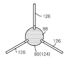
또한, 도 8 및 도 9에 나타내는 제 5 실시예의 경우에는 상기의 제 4 실시예와는 반대로, 막 방착 부재(80)로서는 외경이 제 1 조사창(26A)보다도 훨씬 작은 원형형상의 석영 유리판(124)을 이용하고 있다. 이 작은 원형형상의 석영 유리판(124)은 천장부(6A)로부터 개구부(22A)의 중심측을 향해 연정한 복수개, 예를 들면, 3개의 지지 아암(126)에 의해, 제 1 조사창(26A)의 중심부에 대응하는 위치에서 지지되어 있다. 이 석영 유리판(124)의 직경 W2는 제 1 조사창(26A)에 퇴적하는 불필요한 막의 막두께 분포에 따라 정해진다.In addition, in the case of the fifth embodiment shown in FIGS. 8 and 9, in contrast to the fourth embodiment described above, the
이 제 5 실시예는 제 1 조사창(26A)의 하면의 중심부에 불필요한 박막이, 특히, 두껍게 퇴적하는 바와 같은 어닐 처리를 실행할 때에 이용한다. 이 경우, 도 9a에 나타내는 바와 같이, 이 원형형상의 석영 유리판(124)의 전체를 차광부(86)로 해도 좋고, 반대로 도 9b에 나타내는 바와 같이, 이 원형 링형상의 석영 유리판(124)의 전체를 투과 영역(88)으로 해도 좋다. This fifth embodiment is used when an unnecessary thin film is particularly deposited at the center of the lower surface of the
이 제 5 실시예에서는 상기의 제 1 내지 제 3 실시예에서 설명한 기술을 모두 적용할 수 있고, 또한 제 1 내지 제 3 실시예에서 설명한 바와 같은 작용 효과를 발휘할 수 있다. 이 제 5 실시예에서는 피처리체인 반도체 웨이퍼 W를 지지하는 지지 수단(38)과 조사창(제 1 조사창(26A))의 사이에, 피처리체의 표면의 일부에 대응하는 크기로 설정한 석영 유리판(124)으로 이루어지는 막 방착 부재(80)를 마련하는 것에 의해, 예를 들면, 피처리체로부터 방출되는 물질이 많이 부착되는 영역에 대응시켜 국부적으로 막 방착 부재를 마련할 수 있고, 조사 효율을 높게 유지하면서 조사창에 흐릿함이 발생하는 것을 억제할 수 있다. 단, 이 제 5 실시예의 경우에는 제 1 조사창(26A)의 주변부에 약간 불필요한 막이 퇴적하는 것은 피할 수 없지만, 작은 원형형상의 석영 유리판(124)의 주변부에는 아무것도 마련하고 있지 않으므로, 이 부분에 있어서의 열선의 흡수가 없고, 그만큼, 반도체 웨이퍼의 가열 효율을 높일 수 있다. In this fifth embodiment, all of the techniques described in the first to third embodiments described above can be applied, and the same effects as described in the first to third embodiments can be obtained. In this fifth embodiment, quartz is set to a size corresponding to a part of the surface of the object between the support means 38 for supporting the semiconductor wafer W as the object to be treated and the irradiation window (the
(제 6 실시예)(Sixth Embodiment)
다음으로, 본 발명의 제 6 실시예에 대해 설명한다. Next, a sixth embodiment of the present invention will be described.
상기의 제 1∼제 5 실시예에서는 제 1 조사창(26A)의 표면에 불필요한 막이 부착되는 것을 방지하기 위해, 막 방착 부재(80)를 마련했지만, 이 제 6 실시예에서는 상기 막 방착 부재(80)를 이용하지 않고, 상기 반도체 웨이퍼와 모의 웨이퍼의 설치 위치를 상하 교체하는 것에 의해, 상기 모의 웨이퍼에 막 방착 부재의 기능을 겸용시키고 있다. 이 제 6 실시예는 미러링 제어를 실행하는 도 4에 나타내는 제 2 실시예의 변형 실시예이다. In the first to fifth embodiments described above, the
도 10은 이와 같은 본 발명의 열처리 장치의 제 6 실시형태를 나타내는 단면도이다. 또한, 도 1 내지 도 4에 나타내는 구성 부분과 동일 구성 부분에 대해서는 동일 참조 부호를 붙여 그 설명을 생략한다. 이 제 6 실시형태에서는, 상술한 바와 같이, 상기 설명한 바와 같은 막 방착 부재(80)를 마련하고 있지 않고, 반도체 웨이퍼 W와 모의 웨이퍼(102)의 설치 위치를 상하 반대로 해서 교체하고 있으며, 따라서, 반도체 웨이퍼 W의 바로 위쪽에 모의 웨이퍼(102)가 설치되어 있다. 10 is a cross-sectional view showing the sixth embodiment of such a heat treatment apparatus of the present invention. In addition, about the component same as the component shown in FIGS. 1-4, the same code | symbol is attached | subjected and the description is abbreviate | omitted. In the sixth embodiment, as described above, the
즉, 반도체 웨이퍼 W는 도 1에 나타내는 제 1 실시예와 같이 승강판(42)으로부터 연장하는 지지암(62)의 선단에 마련한 지지 핀(64)에 의해 지지되어 있다. 이 경우, 이 지지 핀(64)의 길이는 도 1의 경우보다도 조금 짧게 설정되어 있다. 또한, 이 반도체 웨이퍼 W의 위쪽에 위치되는 모의 웨이퍼(102)는 처리용기(6)의 측벽으로부터 연장하는 복수개의 지지암(128)에 의해서 지지되어 있다. 따라서, 위쪽에 위치하는 제 1 가열 수단(28A)에 의해 상기 모의 웨이퍼(102)를 가열하고, 아래쪽에 설치하는 제 2 가열 수단(28B)에 의해 반도체 웨이퍼 W를 가열하도록 되어 있다. 그리고, 온도 측정기(34)는 제 1 가열 수단(28A)측에 마련하여, 상기 모의 웨이퍼(102)의 상면측의 온도를 측정하도록 되어 있고, 상기 온도 제어부(36)는 미러링 제어를 실행하게 된다.That is, the semiconductor wafer W is supported by the
따라서, 이 경우에는 상기 모의 웨이퍼(102)와 이 위쪽의 제 1 조사창(26A) 사이의 거리 L3과, 상기 반도체 웨이퍼 W와 이 아래쪽의 제 2 조사창(26B) 사이의 거리 L4가 동일하게 되도록 설정되어 있다. In this case, therefore, the distance L3 between the
이 제 6 실시예의 경우에는 온도 측정기(34)는 모의 웨이퍼(102)의 상면의 온도를 측정하고, 이 측정값에 의거하여 도 4에 나타내는 제 2 실시예에서 설명한 바와 같은 미러링 제어가 실행된다. 이 경우, 어닐 처리시에 반도체 웨이퍼 W의 박막으로부터 발생한 물질은 화살표 ‘130’으로 나타내는 바와 같이 상승해서 모의 웨이퍼(102)의 하면(이면)에 부착 퇴적하게 된다. 따라서, 제 1 조사창(26A)의 표면(상면)에 불필요한 막이 부착되는 일은 없으며, 이것에 흐릿함이 발생하는 것을 방지할 수 있다. In the case of the sixth embodiment, the
또한, 상기한 이유에 의해 방사 온도계로 이루어지는 온도 측정기(34)의 측정 대상으로 되는 모의 웨이퍼(102)의 상면에는 불필요한 막이 퇴적하는 일은 없으므로, 이 모의 웨이퍼(102)의 상면의 표면 상태는 항상 안정적으로 유지되게 되고, 이 온도 측정의 정밀도를 높게 유지할 수 있다. In addition, since the film | membrane does not accumulate on the upper surface of the
이와 같이, 이 제 6 실시예에 의하면, 피처리체인 반도체 웨이퍼 W의 위쪽에 모의 피처리체인 모의 웨이퍼(102)를 배치하고, 상기 모의 웨이퍼(102)의 상면측의 온도를 측정하면서, 소위 미러링 제어를 실행하도록 했으므로, 반도체 웨이퍼의 박막으로부터 발생한 물질을 상기 모의 웨이퍼의 하면(이면)에 퇴적시킬 수 있고, 따라서, 상기한 막 방착 부재(80)를 이용하는 일 없이, 제 1 조사창(26A)에 불필요한 부착막에 기인하는 흐릿함이 발생하는 것을 방지할 수 있다. As described above, according to the sixth embodiment, the so-called mirroring is performed while arranging the
또한, 이상 설명한 각 실시예에 있어서는 가열 수단(28A, 28B)으로서 가열 램프(32A, 32B)를 이용했지만, 이것에 한정되지 않고, 레이저 광을 이용하여 주사시키도록 해도 좋다. In addition, although the
또, 어닐 처리의 대상으로 되는 박막은 가열에 의해 불필요한 막의 부착이 발생하는 바와 같은 모든 종류의 막이며, 이와 같은 막이 형성되는 열처리 장치에 대해 본 발명을 적용할 수 있다. 또한, 여기서는 피처리체로서 반도체 웨이퍼를, 예로 들어, 설명했지만, 이것에 한정되지 않고, 유리 기판, LCD 기판, 세라믹 기판 등에도 본 발명을 적용할 수 있다. The thin film to be subjected to the annealing treatment is any kind of film in which unnecessary adhesion of the film occurs by heating, and the present invention can be applied to a heat treatment apparatus in which such a film is formed. In addition, although the semiconductor wafer was demonstrated as an example as a to-be-processed object here, it is not limited to this, The invention can be applied also to a glass substrate, an LCD substrate, a ceramic substrate, etc.
Claims (21)
상기 피처리체를 수용 가능한 동시에 천장부를 갖는 처리용기와,
상기 처리용기내에 마련되고, 상기 피처리체를 지지하는 지지 수단과,
상기 처리용기의 상기 천장부에 마련된 제 1 조사창과,
상기 제 1 조사창의 외측에 마련되고, 가열용의 열선을 발하는 제 1 가열 수단과,
상기 처리용기에 마련되고, 상기 처리용기내에 소정의 가스를 공급하는 가스 공급 수단과,
상기 처리용기에 마련되고, 상기 처리용기내의 분위기를 배기하는 배기 수단과,
상기 지지 수단과 상기 제 1 조사창의 사이에 마련되고, 그 일부에 상기 열선의 일부 혹은 전부를 차단하기 위한 차광부가 형성된 막 방착 부재
를 구비한 것을 특징으로 하는 열처리 장치.
In the heat treatment apparatus which performs a predetermined | prescribed heat processing with respect to a to-be-processed object,
A processing container capable of accommodating the object to be processed and having a ceiling portion;
Support means provided in the processing container and supporting the object to be processed;
A first irradiation window provided in the ceiling of the processing container;
First heating means provided outside the first irradiation window and emitting a heating wire for heating;
Gas supply means which is provided in the processing container and supplies a predetermined gas into the processing container;
Exhaust means provided in the processing container, and exhausting an atmosphere in the processing container;
It is provided between the said support means and a said 1st irradiation window, The film | membrane adhesion member provided with the light-shielding part for blocking a part or all of the said heating wire in the one part.
Heat treatment apparatus comprising a.
상기 막 방착 부재는 석영 유리판을 포함하는 것을 특징으로 하는 열처리 장치.
The method of claim 1,
And the film adhesion member comprises a quartz glass plate.
상기 차광부는 상기 막 방착 부재의 주변부에 링형상으로 형성되어 있는 것을 특징으로 하는 열처리 장치.
The method of claim 1,
And said light shielding portion is formed in a ring shape at a periphery of said film adhesion member.
상기 차광부는 상기 막 방착 부재의 중앙부에 원형형상으로 형성되어 있는 것을 특징으로 하는 열처리 장치.
The method of claim 1,
And the light shielding portion is formed in a circular shape at a central portion of the film adhesion member.
상기 차광부는 불투명 유리 상태로 이루어져 있는 것을 특징으로 하는 열처리 장치.
The method of claim 2,
And the light shielding portion is made of an opaque glass state.
상기 막 방착 부재에, 상기 제 1 조사창의 하면과 상기 막 방착 부재의 상면의 사이에서 구획 형성되는 공간에 연통되는 압력 조정 연락로가 형성되어 있는 것을 특징으로 하는 열처리 장치.
The method of claim 1,
And a pressure regulating contact passage communicating with the space formed between the lower surface of the first irradiation window and the upper surface of the membrane adhesion member, in the membrane adhesion member.
상기 피처리체를 수용 가능한 동시에 천장부를 갖는 처리용기와,
상기 처리용기내에 마련되고, 상기 피처리체를 지지하는 지지 수단과,
상기 처리용기의 상기 천장부에 마련된 제 1 조사창과,
상기 제 1 조사창의 외측에 마련되고, 가열용의 열선을 발하는 제 1 가열 수단과,
상기 처리용기에 마련되고, 상기 처리용기내에 소정의 가스를 공급하는 가스 공급 수단과,
상기 처리용기에 마련되고, 상기 처리용기내의 분위기를 배기하는 배기 수단과,
상기 지지 수단과 상기 제 1 조사창의 사이에 마련되는 동시에 상기 피처리체의 표면의 일부에 대응하는 크기로 설정된 막 방착 부재
를 구비한 것을 특징으로 하는 열처리 장치.
In the heat treatment apparatus which performs a predetermined | prescribed heat processing with respect to a to-be-processed object,
A processing container capable of accommodating the object to be processed and having a ceiling portion;
Support means provided in the processing container and supporting the object to be processed;
A first irradiation window provided in the ceiling of the processing container;
First heating means provided outside the first irradiation window and emitting a heating wire for heating;
Gas supply means which is provided in the processing container and supplies a predetermined gas into the processing container;
Exhaust means provided in the processing container, and exhausting an atmosphere in the processing container;
A film adhesion member provided between the supporting means and the first irradiation window and set to a size corresponding to a part of the surface of the object to be processed.
Heat treatment apparatus comprising a.
상기 막 방착 부재는 상기 피처리체의 주변부에 대응하는 크기로 링형상으로 형성되어 있고, 상기 막 방착 부재는 링형상으로 이루어진 석영 유리를 갖는 것을 특징으로 하는 열처리 장치.
The method of claim 7, wherein
And the membrane anti-corrosion member is formed in a ring shape with a size corresponding to the periphery of the object to be processed, and the membrane anti-corrosion member has a quartz glass made of a ring shape.
상기 막 방착 부재는 상기 피처리체의 중앙부에 대응하는 크기로 원형형상으로 형성되고, 상기 막 방착 부재는 원판형상으로 이루어진 석영 유리를 갖는 것을 특징으로 하는 열처리 장치.
The method of claim 7, wherein
And the film adhesion member is formed in a circular shape with a size corresponding to the central portion of the object to be processed, and the film adhesion member has a quartz glass having a disk shape.
상기 석영 유리는 투명하게 이루어져 있는 것을 특징으로 하는 열처리 장치.
The method of claim 8,
The heat treatment apparatus, characterized in that the quartz glass is made transparent.
상기 석영 유리는 상기 열선의 일부 혹은 전부를 차단하기 위해 불투명 상태로 이루어져 있는 것을 특징으로 하는 열처리 장치.
The method of claim 8,
And the quartz glass is made in an opaque state to block some or all of the hot wire.
상기 가열 수단은 가열 램프를 포함하는 것을 특징으로 하는 열처리 장치.
The method of claim 1,
And said heating means comprise a heating lamp.
상기 소정의 열처리는 상기 피처리체의 표면에 형성되어 있는 박막을 가열하는 어닐 처리인 것을 특징으로 하는 열처리 장치.
The method of claim 1,
The predetermined heat treatment is an annealing treatment for heating a thin film formed on the surface of the workpiece.
상기 피처리체를 수용 가능한 동시에 천장부 및 바닥부를 갖는 처리용기와,
상기 처리용기내에 마련되고, 상기 피처리체를 지지하는 지지 수단과,
상기 피처리체의 위쪽에 있으며 상기 피처리체와 대향되도록 지지된 모의 피처리체와,
상기 처리용기의 상기 천장부에 마련된 제 1 조사창과,
상기 제 1 조사창의 외측에 마련되고, 가열용의 열선을 발하는 제 1 가열 수단과,
상기 처리용기의 상기 바닥부에 마련된 제 2 조사창과,
상기 제 2 조사창의 외측에 마련되고, 가열용의 열선을 발하는 제 2 가열 수단과,
상기 처리용기에 마련되고, 상기 처리용기내에 소정의 가스를 공급하는 가스 공급 수단과,
상기 처리용기에 마련되고, 상기 처리용기내의 분위기를 배기하는 배기 수단과,
상기 모의 피처리체의 온도를 측정하는 온도 측정기와,
상기 온도 측정기에 접속되고, 상기 온도 측정기의 측정값에 의거하여 상기 제 1 및 제 2 가열 수단을 제어하는 온도 제어부
를 구비한 것을 특징으로 하는 열처리 장치.
In the heat treatment apparatus which performs a predetermined | prescribed heat processing with respect to a to-be-processed object,
A processing container capable of accommodating the object to be processed and having a ceiling and a bottom;
Support means provided in the processing container and supporting the object to be processed;
A simulated to-be-processed object located above the to-be-processed object and supported to face the to-be-processed object,
A first irradiation window provided in the ceiling of the processing container;
First heating means provided outside the first irradiation window and emitting a heating wire for heating;
A second irradiation window provided in the bottom portion of the processing container;
2nd heating means provided in the outer side of a said 2nd irradiation window, and radiating the heating wire for heating,
Gas supply means which is provided in the processing container and supplies a predetermined gas into the processing container;
Exhaust means provided in the processing container, and exhausting an atmosphere in the processing container;
A temperature measuring device for measuring a temperature of the simulated target object;
A temperature control unit connected to the temperature measuring unit and controlling the first and second heating means based on the measured value of the temperature measuring unit
Heat treatment apparatus comprising a.
상기 온도 측정기는 상기 모의 피처리체의 상면에 대향시켜 마련된 방사 온도계로 이루어지는 것을 특징으로 하는 열처리 장치.
The method of claim 14,
And the temperature measuring device comprises a radiation thermometer provided to face an upper surface of the simulated object.
상기 지지 수단은 상기 피처리체를 회전시키는 회전 기구를 갖고 있는 것을 특징으로 하는 열처리 장치.
The method of claim 14,
And said support means has a rotating mechanism for rotating said object to be processed.
상기 모의 피처리체는 고정적으로 마련되어 있는 것을 특징으로 하는 열처리 장치.
The method of claim 14,
The said to-be-processed object is fixedly provided, The heat processing apparatus characterized by the above-mentioned.
상기 모의 피처리체와 상기 제 1 가열 수단 사이의 거리와, 상기 피처리체와 상기 제 2 가열 수단 사이의 거리는 동일하게 되도록 설정되어 있는 것을 특징으로 하는 열처리 장치.
The method of claim 14,
The distance between the said to-be-processed object and the said 1st heating means, and the distance between the to-be-processed object and the said 2nd heating means are set so that it may become the same.
상기 온도 제어부는 상기 제 1 가열 수단과 상기 제 2 가열 수단이 서로 동일한 열량을 방사하도록 제어하는 것을 특징으로 하는 열처리 장치.
The method of claim 14,
And the temperature control unit controls the first heating means and the second heating means to radiate the same amount of heat to each other.
상기 가열 수단은 가열 램프를 포함하는 것을 특징으로 하는 열처리 장치.
The method of claim 14,
And said heating means comprise a heating lamp.
상기 소정의 열처리는 상기 피처리체의 표면에 형성되어 있는 박막을 가열하는 어닐 처리인 것을 특징으로 하는 열처리 장치.The method of claim 14,
The predetermined heat treatment is an annealing treatment for heating a thin film formed on the surface of the workpiece.
Applications Claiming Priority (2)
| Application Number | Priority Date | Filing Date | Title |
|---|---|---|---|
| JPJP-P-2008-089069 | 2008-03-31 | ||
| JP2008089069A JP5077018B2 (en) | 2008-03-31 | 2008-03-31 | Heat treatment equipment |
Publications (1)
| Publication Number | Publication Date |
|---|---|
| KR20100138984A true KR20100138984A (en) | 2010-12-31 |
Family
ID=41135299
Family Applications (1)
| Application Number | Title | Priority Date | Filing Date |
|---|---|---|---|
| KR1020107021779A KR20100138984A (en) | 2008-03-31 | 2009-03-18 | Heat treatment apparatus |
Country Status (5)
| Country | Link |
|---|---|
| JP (1) | JP5077018B2 (en) |
| KR (1) | KR20100138984A (en) |
| CN (1) | CN101855708B (en) |
| TW (1) | TW200949950A (en) |
| WO (1) | WO2009122913A1 (en) |
Cited By (2)
| Publication number | Priority date | Publication date | Assignee | Title |
|---|---|---|---|---|
| KR101297981B1 (en) * | 2011-10-07 | 2013-08-23 | (주) 예스티 | Heat process chamber for substrate |
| KR20220033432A (en) * | 2020-09-09 | 2022-03-16 | 가부시키가이샤 스크린 홀딩스 | Heat treatment apparatus |
Families Citing this family (13)
| Publication number | Priority date | Publication date | Assignee | Title |
|---|---|---|---|---|
| JP5466670B2 (en) * | 2010-10-28 | 2014-04-09 | 株式会社日立国際電気 | Substrate processing apparatus and semiconductor device manufacturing method |
| JP5640890B2 (en) * | 2011-05-23 | 2014-12-17 | ウシオ電機株式会社 | Light irradiation apparatus and light irradiation method |
| JP6038503B2 (en) * | 2011-07-01 | 2016-12-07 | 株式会社日立国際電気 | Substrate processing apparatus and semiconductor device manufacturing method |
| JP5964630B2 (en) * | 2012-03-27 | 2016-08-03 | 株式会社Screenホールディングス | Heat treatment equipment |
| US8785815B2 (en) * | 2012-06-22 | 2014-07-22 | Applied Materials, Inc. | Aperture control of thermal processing radiation |
| CN105261576A (en) * | 2014-07-15 | 2016-01-20 | 北京北方微电子基地设备工艺研究中心有限责任公司 | Heating chamber and semiconductor processing equipment |
| US11089657B2 (en) * | 2015-03-06 | 2021-08-10 | SCREEN Holdings Co., Ltd. | Light-irradiation heat treatment apparatus |
| JP6518548B2 (en) * | 2015-08-10 | 2019-05-22 | 東京応化工業株式会社 | UV irradiation apparatus, resist pattern forming apparatus, UV irradiation method and resist pattern forming method |
| JP6546512B2 (en) * | 2015-11-04 | 2019-07-17 | 株式会社Screenホールディングス | Heat treatment equipment |
| CN107706139A (en) * | 2017-11-13 | 2018-02-16 | 上海华力微电子有限公司 | A kind of temperature control equipment of semiconductor processing tools |
| JP7048372B2 (en) * | 2018-03-20 | 2022-04-05 | 株式会社Screenホールディングス | Heat treatment equipment and heat treatment method |
| KR20210075482A (en) | 2019-12-13 | 2021-06-23 | 삼성전자주식회사 | Process Apparatus Having a Non-Contact Thermo-Sensor |
| CN115064471B (en) * | 2022-08-01 | 2023-11-28 | 北京屹唐半导体科技股份有限公司 | Wafer heat treatment device |
Family Cites Families (4)
| Publication number | Priority date | Publication date | Assignee | Title |
|---|---|---|---|---|
| JPH09270390A (en) * | 1996-03-29 | 1997-10-14 | Dainippon Screen Mfg Co Ltd | Device for processing wafer by light irradiation |
| JPH10321547A (en) * | 1997-05-22 | 1998-12-04 | Kokusai Electric Co Ltd | Heat-treating device |
| JP4200844B2 (en) * | 2003-08-11 | 2008-12-24 | 東京エレクトロン株式会社 | Heat treatment equipment |
| JP2006005177A (en) * | 2004-06-17 | 2006-01-05 | Tokyo Electron Ltd | Thermal treatment apparatus |
-
2008
- 2008-03-31 JP JP2008089069A patent/JP5077018B2/en active Active
-
2009
- 2009-03-18 KR KR1020107021779A patent/KR20100138984A/en not_active Application Discontinuation
- 2009-03-18 WO PCT/JP2009/055325 patent/WO2009122913A1/en active Application Filing
- 2009-03-18 CN CN200980100966XA patent/CN101855708B/en not_active Expired - Fee Related
- 2009-03-30 TW TW98110446A patent/TW200949950A/en unknown
Cited By (2)
| Publication number | Priority date | Publication date | Assignee | Title |
|---|---|---|---|---|
| KR101297981B1 (en) * | 2011-10-07 | 2013-08-23 | (주) 예스티 | Heat process chamber for substrate |
| KR20220033432A (en) * | 2020-09-09 | 2022-03-16 | 가부시키가이샤 스크린 홀딩스 | Heat treatment apparatus |
Also Published As
| Publication number | Publication date |
|---|---|
| TW200949950A (en) | 2009-12-01 |
| CN101855708B (en) | 2012-10-10 |
| JP5077018B2 (en) | 2012-11-21 |
| JP2009246061A (en) | 2009-10-22 |
| WO2009122913A1 (en) | 2009-10-08 |
| CN101855708A (en) | 2010-10-06 |
Similar Documents
| Publication | Publication Date | Title |
|---|---|---|
| KR20100138984A (en) | Heat treatment apparatus | |
| KR960003155B1 (en) | Multi-chamber type cvd device and its substrate processing method | |
| KR100257105B1 (en) | Film processing apparatus | |
| US6506253B2 (en) | Photo-excited gas processing apparatus for semiconductor process | |
| JP5982758B2 (en) | Microwave irradiation device | |
| TWI782760B (en) | A coated liner assembly for a semiconductor processing chamber | |
| US20110155058A1 (en) | Substrate processing apparatus having a radiant cavity | |
| US10405376B2 (en) | Apparatus and method for treating substrate | |
| JPH11204442A (en) | Single wafer heat treatment device | |
| KR20130087530A (en) | Transparent reflector plate for rapid thermal processing chamber | |
| TWI579922B (en) | Methods and apparatus for processing a substrate | |
| JP2006005177A (en) | Thermal treatment apparatus | |
| WO2019053807A1 (en) | Substrate treatment apparatus, heater apparatus, and semiconductor device manufacturing process | |
| JP3551609B2 (en) | Heat treatment equipment | |
| JP4806856B2 (en) | Heat treatment method and heat treatment apparatus | |
| JP7214834B2 (en) | Semiconductor device manufacturing method, substrate processing apparatus, and program | |
| JP2007005399A (en) | Substrate processing apparatus | |
| CN114127897A (en) | Heat insulating structure, substrate processing apparatus, and method for manufacturing semiconductor device | |
| JP2002367914A (en) | Heat treatment device | |
| KR100839678B1 (en) | Sheet-type treating device | |
| JP2006237516A (en) | Substrate treatment equipment | |
| JPH11204443A (en) | Single wafer heat treatment device | |
| JP2010086985A (en) | Wafer-processing apparatus | |
| JP2005259902A (en) | Substrate processor | |
| JP3073728B2 (en) | Single wafer type heat treatment equipment |
Legal Events
| Date | Code | Title | Description |
|---|---|---|---|
| A201 | Request for examination | ||
| E601 | Decision to refuse application |