KR20100126284A - Method of forming a heatsink - Google Patents
Method of forming a heatsink Download PDFInfo
- Publication number
- KR20100126284A KR20100126284A KR1020107016985A KR20107016985A KR20100126284A KR 20100126284 A KR20100126284 A KR 20100126284A KR 1020107016985 A KR1020107016985 A KR 1020107016985A KR 20107016985 A KR20107016985 A KR 20107016985A KR 20100126284 A KR20100126284 A KR 20100126284A
- Authority
- KR
- South Korea
- Prior art keywords
- heat sink
- metal material
- tpg
- formation method
- sink formation
- Prior art date
Links
Images


Classifications
-
- H—ELECTRICITY
- H05—ELECTRIC TECHNIQUES NOT OTHERWISE PROVIDED FOR
- H05K—PRINTED CIRCUITS; CASINGS OR CONSTRUCTIONAL DETAILS OF ELECTRIC APPARATUS; MANUFACTURE OF ASSEMBLAGES OF ELECTRICAL COMPONENTS
- H05K7/00—Constructional details common to different types of electric apparatus
- H05K7/20—Modifications to facilitate cooling, ventilating, or heating
- H05K7/2039—Modifications to facilitate cooling, ventilating, or heating characterised by the heat transfer by conduction from the heat generating element to a dissipating body
- H05K7/20509—Multiple-component heat spreaders; Multi-component heat-conducting support plates; Multi-component non-closed heat-conducting structures
-
- G—PHYSICS
- G06—COMPUTING; CALCULATING OR COUNTING
- G06F—ELECTRIC DIGITAL DATA PROCESSING
- G06F1/00—Details not covered by groups G06F3/00 - G06F13/00 and G06F21/00
- G06F1/16—Constructional details or arrangements
- G06F1/20—Cooling means
-
- H—ELECTRICITY
- H01—ELECTRIC ELEMENTS
- H01L—SEMICONDUCTOR DEVICES NOT COVERED BY CLASS H10
- H01L21/00—Processes or apparatus adapted for the manufacture or treatment of semiconductor or solid state devices or of parts thereof
- H01L21/02—Manufacture or treatment of semiconductor devices or of parts thereof
- H01L21/04—Manufacture or treatment of semiconductor devices or of parts thereof the devices having at least one potential-jump barrier or surface barrier, e.g. PN junction, depletion layer or carrier concentration layer
- H01L21/48—Manufacture or treatment of parts, e.g. containers, prior to assembly of the devices, using processes not provided for in a single one of the subgroups H01L21/06 - H01L21/326
- H01L21/4814—Conductive parts
- H01L21/4871—Bases, plates or heatsinks
- H01L21/4882—Assembly of heatsink parts
-
- H—ELECTRICITY
- H01—ELECTRIC ELEMENTS
- H01L—SEMICONDUCTOR DEVICES NOT COVERED BY CLASS H10
- H01L23/00—Details of semiconductor or other solid state devices
- H01L23/34—Arrangements for cooling, heating, ventilating or temperature compensation ; Temperature sensing arrangements
- H01L23/36—Selection of materials, or shaping, to facilitate cooling or heating, e.g. heatsinks
- H01L23/367—Cooling facilitated by shape of device
-
- H—ELECTRICITY
- H01—ELECTRIC ELEMENTS
- H01L—SEMICONDUCTOR DEVICES NOT COVERED BY CLASS H10
- H01L23/00—Details of semiconductor or other solid state devices
- H01L23/34—Arrangements for cooling, heating, ventilating or temperature compensation ; Temperature sensing arrangements
- H01L23/36—Selection of materials, or shaping, to facilitate cooling or heating, e.g. heatsinks
- H01L23/373—Cooling facilitated by selection of materials for the device or materials for thermal expansion adaptation, e.g. carbon
-
- F—MECHANICAL ENGINEERING; LIGHTING; HEATING; WEAPONS; BLASTING
- F28—HEAT EXCHANGE IN GENERAL
- F28F—DETAILS OF HEAT-EXCHANGE AND HEAT-TRANSFER APPARATUS, OF GENERAL APPLICATION
- F28F13/00—Arrangements for modifying heat-transfer, e.g. increasing, decreasing
-
- H—ELECTRICITY
- H01—ELECTRIC ELEMENTS
- H01L—SEMICONDUCTOR DEVICES NOT COVERED BY CLASS H10
- H01L2924/00—Indexing scheme for arrangements or methods for connecting or disconnecting semiconductor or solid-state bodies as covered by H01L24/00
- H01L2924/0001—Technical content checked by a classifier
- H01L2924/0002—Not covered by any one of groups H01L24/00, H01L24/00 and H01L2224/00
-
- H—ELECTRICITY
- H01—ELECTRIC ELEMENTS
- H01L—SEMICONDUCTOR DEVICES NOT COVERED BY CLASS H10
- H01L2924/00—Indexing scheme for arrangements or methods for connecting or disconnecting semiconductor or solid-state bodies as covered by H01L24/00
- H01L2924/30—Technical effects
- H01L2924/301—Electrical effects
- H01L2924/3011—Impedance
-
- Y—GENERAL TAGGING OF NEW TECHNOLOGICAL DEVELOPMENTS; GENERAL TAGGING OF CROSS-SECTIONAL TECHNOLOGIES SPANNING OVER SEVERAL SECTIONS OF THE IPC; TECHNICAL SUBJECTS COVERED BY FORMER USPC CROSS-REFERENCE ART COLLECTIONS [XRACs] AND DIGESTS
- Y10—TECHNICAL SUBJECTS COVERED BY FORMER USPC
- Y10T—TECHNICAL SUBJECTS COVERED BY FORMER US CLASSIFICATION
- Y10T29/00—Metal working
- Y10T29/49—Method of mechanical manufacture
- Y10T29/4935—Heat exchanger or boiler making
- Y10T29/49393—Heat exchanger or boiler making with metallurgical bonding
Abstract
본 발명은 히트싱크를 형성하기 위해서 열분해 흑연(thermo pyrolytic graphite; TPG) 요소(100)를 적어도 하나의 제 1 금속 재료(200)에 접착시키는 방법에 관한 것이다. 히트싱크는 X-Y 평면에 개선된 열 전도성을 갖고 있다.The present invention relates to a method of adhering thermo pyrolytic graphite (TPG) element 100 to at least one first metal material 200 to form a heat sink. Heat sinks have improved thermal conductivity in the X-Y plane.
Description
본 발명은 일반적으로 다양한 용도의 히트싱크(heatsink)로서 기능하는 금속 재료에 열분해 흑연(thermo pyrolytic graphite; TPG)을 접착시키는 방법에 관한 것이며, 특히 히트싱크로서 사용하기 위한 금속 열전도성 구조체를 형성하기 위해 적어도 하나의 금속 재료에 TPG 요소를 접착시키는 것에 관한 것이다.FIELD OF THE INVENTION The present invention relates generally to a method for bonding thermopyrolytic graphite (TPG) to a metal material that functions as a heatsink for a variety of uses, and in particular to forming a metal thermally conductive structure for use as a heatsink. For adhering the TPG element to at least one metallic material.
현대의 매설형 컴퓨터 시스템은 체적적으로 제한된 환경내에 매우 높은 열적 파워 전기 구성부품(thermo power electrical component)을 수납한다. 이러한 구성부품의 파워 소산이 증가할 때 통상적으로 체적이 변화되지 않는데, 이것은 구성부품의 온도 관리에 있어서 상당한 문제가 된다. 종래에는, 온도 상승을 제어하기 위해서, 알루미늄 및/또는 구리 등의 높은 열전도성 재료로 구성된 능동형 또는 수동형 히트싱크와 같은 각종의 직접 냉각 기술이 사용되어 왔다. 그러나, 이들 재료는, 비교적 많은 양의 표면적이 기류에 노출된 경우에만 만족스러우므로, 이용가능한 전체 체적의 상당량을 차지하는 물리적으로 큰 히트싱크 구조체를 필요로 한다. 히트싱크의 물리적 크기가 증가함에 따라서, 히트싱크의 말단부로 열을 신속하게 운반함으로써, 열을 기류에 노출시키는 재료의 능력은 감소된다.Modern buried computer systems house very high thermal power electrical components in a volume constrained environment. As the power dissipation of such components increases, the volume typically does not change, which is a significant problem in temperature management of the components. Conventionally, various direct cooling techniques, such as active or passive heat sinks composed of high thermally conductive materials such as aluminum and / or copper, have been used to control the temperature rise. However, these materials are only satisfactory when a relatively large amount of surface area is exposed to airflow and therefore requires a physically large heatsink structure that occupies a significant amount of the total available volume. As the physical size of the heatsink increases, by rapidly transporting heat to the distal end of the heatsink, the ability of the material to expose heat to airflow is reduced.
열분해 흑연(TPG) 재료는 종래의 금속 재료에 비하여 단일 (X-Y) 평면에서의 개선된 열전도 능력을 갖는 것으로 알려져 있다. 또한, TPG는 구리에 비하여 개선된 전체 열전도성을 갖는 것으로 알려져 있다. 최근에, 확산 본딩 프로세스를 사용하여 TPG 재료를 알루미늄 구조체내로 매설하는 방법이 개발되고 있다. TPG 재료와 알루미늄 구조체 사이의 적절한 열 접촉이 생기게 하는 동안의 확산 본딩 프로세스는 TPG-매설형 구조체를 형성하는데 특수 장비가 요구되어 시간 소모적인 프로세스이고 그 결과 제품이 고가로 된다는 점에서 한계가 있다.Pyrolytic graphite (TPG) materials are known to have improved thermal conductivity in a single (X-Y) plane compared to conventional metal materials. TPG is also known to have improved overall thermal conductivity compared to copper. Recently, a method of embedding TPG material into an aluminum structure using a diffusion bonding process has been developed. The diffusion bonding process during the proper thermal contact between the TPG material and the aluminum structure is limited in that it requires a special equipment to form the TPG-embedded structure, which is a time consuming process and as a result the product is expensive.
따라서, X-Y 평면에서의 효과적인 열전도성을 제공하도록 금속 열전도 구조체(즉, 히트싱크)를 형성하기 위해 알루미늄 구조체와 같은 하나 또는 그 이상의 금속 재료에 접착된 TPG를 갖는 비용 효율적인 제품을 형성하는 방법에 대한 요구가 있다. 또한, 상기 방법이 용이하게 재현 가능하고 많은 다양한 타입의 장비를 사용하여 많은 다양한 설비에서 수행될 수 있을 필요가 있다.Thus, a method for forming a cost effective product having TPG adhered to one or more metal materials, such as an aluminum structure, to form a metal thermally conductive structure (ie, a heat sink) to provide effective thermal conductivity in the XY plane. There is a demand. In addition, the method needs to be easily reproducible and can be carried out in many different facilities using many different types of equipment.
일 실시형태에 있어서, 히트싱크를 형성하기 위해서 열분해 흑연(thermo pyrolytic graphite; TPG)을 제 1 금속 재료 및 제 2 금속 재료에 접착시키는 방법이 제공된다. 이 방법은 TPG 요소를 통해 적어도 하나의 구멍을 형성하는 단계와; 제 1 금속 재료에 적어도 하나의 비아를 형성하는 단계로서, 상기 비아는 TPG 요소를 관통하는 구멍에 상보적으로 되도록 구성되는, 상기 적어도 하나의 비아 형성 단계와; 제 2 금속 재료로 제조된 열 스페이서를 제공하는 단계로서, 상기 열 스페이서는 열 공급원 요소에 상보적으로 되도록 구성되는, 상기 열 스페이서 제공 단계와; TPG 요소의 외부 표면에 금속계 코팅을 도포하는 단계와; 제 1 금속 재료내의 비아 및 제 2 금속 재료의 열 스페이서를 TPG 요소의 코팅된 표면에 접착시키는 단계를 포함한다. 비아, 열 스페이서 및 구멍은 접착되어 히트싱크를 형성하며, 이 히트싱크는 열 공급원 요소로부터의 열을 열 스페이서를 통해 비아로 그리고 TPG 요소내의 구멍을 통해 전도할 수 있도록 구성되어 있다.In one embodiment, a method of adhering thermo pyrolytic graphite (TPG) to a first metal material and a second metal material to form a heat sink is provided. The method includes forming at least one hole through the TPG element; Forming at least one via in the first metallic material, the via configured to be complementary to a hole through the TPG element; Providing a thermal spacer made of a second metal material, the thermal spacer configured to be complementary to a heat source element; Applying a metallic coating to the outer surface of the TPG element; Adhering vias in the first metal material and thermal spacers of the second metal material to the coated surface of the TPG element. Vias, thermal spacers, and holes are bonded to form a heatsink, which is configured to conduct heat from the heat source element to the vias through the thermal spacers to the vias and through the holes in the TPG element.
다른 실시형태에 있어서, 히트싱크를 형성하기 위해서 열분해 흑연(thermo pyrolytic graphite; TPG)을 제 1 금속 재료 및 제 2 금속 재료에 접착시키는 방법이 제공된다. 이 방법은 TPG 요소를 통해 적어도 하나의 구멍을 형성하는 단계와; 제 1 금속 재료에 적어도 하나의 비아를 형성하는 단계로서, 상기 비아는 TPG 요소를 관통하는 구멍에 상보적으로 되도록 구성되는, 상기 적어도 하나의 하나의 비아 형성 단계와; 제 2 금속 재료로 제조된 열 스페이서를 제공하는 단계로서, 상기 열 스페이서는 열 공급원 요소에 상보적으로 되도록 구성되는, 상기 열 스페이서 제공 단계와; 제 1 금속 재료내의 비아 및 제 2 금속 재료의 열 스페이서를 전기도금 프로세스를 이용하여 TPG 요소에 접착시키는 단계를 포함한다. 비아, 열 스페이서 및 구멍은 접착되어 히트싱크를 형성하며, 이 히트싱크는 열 공급원 요소로부터의 열을 열 스페이서를 통해 비아로 그리고 TPG 요소내의 구멍을 통해 전도할 수 있도록 구성되어 있다.In another embodiment, a method is provided for adhering thermo pyrolytic graphite (TPG) to a first metal material and a second metal material to form a heat sink. The method includes forming at least one hole through the TPG element; Forming at least one via in the first metallic material, the via configured to be complementary to a hole through the TPG element; Providing a thermal spacer made of a second metal material, the thermal spacer configured to be complementary to a heat source element; Bonding vias in the first metal material and thermal spacers of the second metal material to the TPG elements using an electroplating process. Vias, thermal spacers, and holes are bonded to form a heatsink, which is configured to conduct heat from the heat source element to the vias through the thermal spacers to the vias and through the holes in the TPG element.
다른 실시형태에 있어서, 히트싱크를 형성하기 위해서 열분해 흑연(thermo pyrolytic graphite; TPG)을 제 1 금속 재료에 접착시키는 방법이 제공된다. 이 방법은 TPG 요소를 통해 적어도 하나의 구멍을 형성하는 단계와; TPG 요소의 외부 표면에 금속계 코팅을 도포하는 단계와; 제 1 금속 재료의 외부 표면에 적어도 하나의 솔더 볼을 부착시키는 단계로서, 상기 솔더 볼은 TPG 요소를 관통한 구멍을 충전하도록 구성된, 상기 부착 단계와; 상기 솔더 볼이 구멍을 충전하도록 제 1 금속 재료를 TPG 요소로 가압하는 단계와; 제 1 금속 재료를 TPG 요소에 납땜하도록 제 1 금속 재료를 가열하는 단계를 포함한다.In another embodiment, a method is provided for adhering thermo pyrolytic graphite (TPG) to a first metal material to form a heat sink. The method includes forming at least one hole through the TPG element; Applying a metallic coating to the outer surface of the TPG element; Attaching at least one solder ball to an outer surface of a first metal material, the solder ball being configured to fill a hole through a TPG element; Forcing the first metal material into the TPG element such that the solder balls fill the holes; Heating the first metal material to solder the first metal material to the TPG element.
도 1은 본 발명의 방법에 따라 접착될 TPG 요소, 제 1 금속 재료 및 제 2 금속 재료를 도시하는 도면,
도 2는 본 발명의 방법에 따른 방법에 사용하기 위해 제 2 금속 재료로 제조된 열 스페이서에 부착된 열 인터페이스 재료를 도시하는 도면,
도 3은 본 발명에 따른 일 실시예의 방법을 이용하여 형성된 히트싱크를 도시하는 도면,
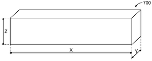
도 4는 히트싱크내의 열 전도성의 X-평면, Y-평면 및 Z-평면을 도시하는 도면,
도 5는 본 발명에 따른 방법에 사용하기 위한 금속 핀(fin) 조립체를 도시하는 도면,
도 6은 본 발명에 따른 제 2 실시예의 방법을 이용하여 형성된 히트싱크를 도시하는 도면.1 shows a TPG element, a first metal material and a second metal material to be bonded according to the method of the present invention;
2 shows a thermal interface material attached to a thermal spacer made of a second metallic material for use in a method according to the method of the present invention;
3 illustrates a heat sink formed using the method of one embodiment according to the present invention;
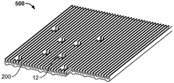
4 illustrates the X-plane, Y-plane, and Z-plane of thermal conductivity in a heat sink;
5 shows a metal fin assembly for use in the method according to the invention, FIG.
6 shows a heat sink formed using the method of the second embodiment according to the present invention;
본 발명은 히트싱크를 형성하기 위해 열분해 흑연(TPG)을 적어도 하나의 금속 재료에 접착하는 것에 관한 것이다. 본 명세서에 사용된 바와 같이, "TPG"는 흑연이 최적의 열 전달을 위한 하나의 방향으로 정렬된 임의의 흑연계 재료(graphite-based material)를 지칭한다. 이들 재료는 통상 "정렬된 흑연(aligned graphite)", "TPG", 및/또는 "고배향성 열분해 흑연(Highly Oriented Pyrolytic Graphite; HOPG)으로 지칭된다. TPG 요소는 금속 열전도 구조체(즉, 히트싱크)의 X-Y 평면에서의 개선된 열전도성을 제공한다. 구체적으로는, 본 발명에 제공된 바와 같은 TPG 요소를 적어도 하나의 금속 재료에 접착하는 방법을 사용함으로써, 컴퓨터 시스템 등의 전기 시스템의 사용중에 발생되는 온도가 종래의 열적 해결책에 비하여 약 12℃ 이상 정도 낮아질 수 있다는 것이 밝혀졌다. 이러한 개선된 온도 방출은 동일한 체적 환경에서의 전기 시스템의 파워 능력을 거의 배가시킨다. 또한, 이러한 파워의 증대에 의해서, 지원될 수 없었던 시스템이 지원될 수 있거나, 기존 시스템을 보다 높은 주위 온도를 갖는 환경에서 사용가능하도록 할 수도 있다.The present invention relates to bonding pyrolytic graphite (TPG) to at least one metallic material to form a heat sink. As used herein, "TPG" refers to any graphite-based material in which graphite is aligned in one direction for optimal heat transfer. These materials are commonly referred to as "aligned graphite", "TPG", and / or "Highly Oriented Pyrolytic Graphite (HOPG). TPG elements are metallic thermal conductive structures (ie, heat sinks). Improved thermal conductivity in the XY plane of, specifically, by using a method of adhering a TPG element to at least one metallic material as provided herein, resulting in the use of an electrical system such as a computer system. It has been found that the temperature can be lowered by about 12 ° C. or more as compared to conventional thermal solutions, such improved temperature release nearly doubles the power capability of the electrical system in the same volume environment. Systems that could not be supported may be supported or may make existing systems available in environments with higher ambient temperatures.
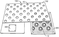
상술한 바와 같이, 히트싱크는 TPG 요소를 적어도 하나의 재료에 접착시킴으로써 형성된다. 일 실시예에 있어서, 도 1 내지 도 3에 도시된 바와 같이, TPG 요소는 히트싱크에 사용하기 위해서 제 1 금속 재료 및 제 2 금속 재료에 접착된다. 이러한 실시예에서, 적어도 하나의 구멍(10)은 TPG(100)를 관통해서 형성된다. 적어도 하나의 비아(12)는 제 1 금속 재료(200)에 형성된다. 제 1 금속 재료(200)에 형성된 비아(12)와, 제 2 금속 재료로 제조된 열 스페이서(300)는 TPG 요소(100)의 코팅된 표면에 접착된다.As mentioned above, the heat sink is formed by adhering the TPG element to at least one material. In one embodiment, as shown in FIGS. 1-3, the TPG element is bonded to the first metal material and the second metal material for use in a heat sink. In this embodiment, at least one
TPG 요소(100)는 TPG 요소를 제조하기 위한 본 기술 분야에 공지된 모든 방법 및/또는 기구를 이용하여 제조될 수 있다. 또한, TPG 요소는 미국 커넥티컷주 윌톤에 소재하는 모멘티브 퍼포먼스 머티리얼(Momentive Performance Material)과 같은 공급자로부터 시중에서 입수가능하다.The
일 실시예에 있어서, 도 1에 도시된 바와 같이, TPG 요소(100)는 평면 TPG 요소로서 구성된다. 특정 실시예에 있어서, TPG 요소(100)는 실질적으로 장방형 형상을 갖는 평면 시트이다. 또한, TPG 요소(100)의 치수는 다양할 수 있는 반면에, 일 실시예에 있어서 TPG 요소(100)는 약 0.06인치의 두께를 갖고 있다.In one embodiment, as shown in FIG. 1, the
적어도 하나의 구멍(10)은 TPG 요소를 관통해 형성된다. 구멍(10)은 본 기술 분야에 공지된 모든 방법을 이용하여 형성될 수 있다. 특정 실시예에 있어서, 도 1에 도시된 바와 같이, 복수의 구멍(10)이 TPG(100)를 관통해 형성된다. TPG 요소(100)를 관통해 형성된 구멍(10)의 치수, 구멍(10)의 개수 및/또는 구멍(10) 사이의 간격은 소망의 최종 제품에 따라 좌우될 것이다. 일 실시예에 있어서, TPG 요소(100)는 적당한 개수의 구멍(10)을 포함하며, 각 구멍은 구멍(10)을 통해 솔더 재료 또는 열 전도성 접착제(사용될 경우)의 유동을 감소시키기 위한 상대적으로 작은 직경을 갖고, TPG 요소(100)의 전기적 및/또는 물리적 결합을 간섭하는 동시에, 충분한 기계적 접착을 형성하도록 솔더 재료 또는 접착제가 구멍(10)을 통과하도록 적당한 직경을 갖고 있다. 또한, 보다 작은 직경의 구멍(10)을 이용함으로써, 모세관 작용 효과가 발생될 수 있으며, 이에 의해 구멍(10)을 통한 솔더 재료 또는 접착제의 보다 나은 위킹 작용(wicking action)을 가능하게 한다.At least one
구멍(10)은 본 기술 분야에 숙련된 자들에게 공지된 모든 적당한 형상일 수 있다. 본 발명의 영역을 제한함이 없이, 각 구멍(10)은 예를 들면 원형, 타원형, 정사각형, 직사각형 또는 삼각형을 포함한 적당한 형상을 가질 수 있다. 일 실시예에 있어서, 각 구멍(10)은 원형 구멍이 제조가 보다 용이하기 때문에 원형 형상이다. 특정 실시예에 있어서, 각 원형 구멍은 대략 0.5인치의 직경을 갖고 있다.The
또한, 적어도 하나의 비아(12)는 제 1 금속 재료(200)에 형성되어 있다. 일 실시예에 있어서, 비아(12)는 TPG 요소(100)를 통해 형성된 상보적인 또는 대응하는 구멍(10)내에 위치되도록 구성된다. 이와 같이, 제 1 금속 재료(20)에 형성된 비아(12)의 치수, 비아(12)의 개수 및/또는 비아(12)사이의 간격은 TPG 요소(100)를 통해 형성된 구멍(10)의 대응하는 치수 및/또는 개수에 따라 좌우된다. 일 실시예에 있어서, 복수의 비아(12)는 도 1에 도시된 바와 같이 제 1 금속 재료(200)를 통해 형성된다.In addition, at least one via 12 is formed in the
특정 실시예에 있어서, 도 1에 도시된 바와 같이, 하나 또는 그 이상의 비아(12)는 TPG 요소(100)를 통해 형성된 구멍(10)을 충전하도록 버튼-형성되도록 구성되어 있다.In a particular embodiment, as shown in FIG. 1, one or
특정 실시예에 있어서, 비아(12)는 하나 또는 그 이상의 개별 버섯-캡 형상 버튼(도시하지 않음)으로 전략적으로 구성된다. 버섯-캡 형상을 이용함으로써, 비아(12)는 TPG 요소(100)와 그리고 그에 따라 열 공급원 요소(도시하지 않음)와의 보다 양호한 접착을 허용하도록 서로로부터 자유롭게 부유된다. 일 실시예에 있어서, 비아(12)가 버섯-캡 형상인 경우, 비아(12)는 줄기를 더 포함한다. 줄기는 구멍(10)을 통해 연장된다. 즉, 줄기는 TPG 요소(100)의 전체 두께를 통해 연장된다. 비아(12)에 대한 다른 적당한 형상은 줄기형 버섯 비아, 즉 줄기만을 갖고 있는 버섯 형상 비아를 포함할 수 있다.In certain embodiments, via 12 is strategically comprised of one or more individual mushroom-cap shaped buttons (not shown). By using the mushroom-cap shape, the
변형 실시예에 있어서, 구멍은 각 비아(12)의 중심을 통해 형성된다. 구멍은 별개의 기계적 커플링 부품이 삽입될 수 있는 크기로 구성될 수 있으며, 이에 의해 제 1 금속 재료(200)와 TPG 요소(100) 사이의 결합을 보강한다. 예를 들면, 일 실시예에 있어서, 구멍은 설명한 바와 같이 제 1 금속 재료(200)의 금속 핀(fin) 또는 전도냉각식 히트프레임을 제 1 금속 재료(200)의 비아(12)에 커플링시키는 것을 용이하게 하기 위한 스크류 또는 리벳을 수용하는 크기로 구성될 수 있다. 기계적 커플링 부품은 접착 이전에, 접착 다음에 또는 접착과 동시에 제공될 수 있다.In a variant embodiment, holes are formed through the center of each via 12. The aperture may be configured to a size into which a separate mechanical coupling component can be inserted, thereby reinforcing the bond between the
제 1 금속 재료(200)는 적당한 열 전도성을 갖는 금속 재료로 제조된다. 예를 들면, 제 1 금속 재료(200)는 알루미늄, 구리, 인듐 및 이들의 조합물을 포함할 수 있다. 일 실시예에 있어서, 제 1 금속 재료(200)는 알루미늄이다. 알루미늄 및 구리 양자는 히트싱크에 사용될 경우 높은 전도성을 제공하는 것으로 알려져 있다. 보다 상세하게, 알루미늄은 히트싱크에 사용될 경우 "Z" 평면에서 양호한 열 전도성을 제공한다. 그러나, 상술한 바와 같이, 알루미늄 및 구리 만으로는 X-Y 평면에서 충분한 열 전달을 제공할 수 없으며, 이와 같이 본 발명은 알루미늄, 구리 또는 이들의 조합물과 조합된 TPG를 갖고 있다. 도 4는 히트싱크(700)의 X 평면, Y 평면 및 Z 평면을 나타내도록 제공된다.The
일 실시예에 있어서, 도 5에 도시된 바와 같이, 제 1 금속 재료(200)는 금속 핀 조립체(400)를 포함한다. 금속 핀 조립체(400)는 열적으로 전도성 금속 재료(200)의 보다 큰 표면적을 제공하며, 이에 의해 열 공급원 요소로부터 효율적이고 유효한 열 방출을 용이하게 한다. 특정 일 실시예에 있어서, 금속 핀 조립체(400)는 대략 6인치 × 5인치이며, 두께는 대략 0.3인치이다. 일 실시예에서 핀 조립체(400)의 핀(2, 4, 6)은 높이가 대략 0.24인치, 두께가 대략 0.024인치이며, 인접한 핀 사이의 간격은 대략 0.096인치이다. 본 기술 분야에 숙련된 자들에 의하면, 핀(2, 4, 6)은 본 발명의 영역을 벗어남이 없이 상술한 것과 다른 크기로 및/이격될 수 있다는 것은 이해될 것이다. 보다 상세하게, 본 기술 분야에 공지된 바와 같이 그리고 제공된 요지에 의해 안내되는 바와 같이 핀 조립체(400)의 핀(2, 4, 6)의 모든 사이즈 및/또는 간격은 본 발명에서 사용될 수 있다.In one embodiment, as shown in FIG. 5, the
제 1 금속 재료(20)가 금속 핀 조립체(400)를 포함할 경우, 제 1 금속 재료(200)에 형성된 비아(12)는 금속 핀 조립체(400)의 핀(2, 4, 6)과 별개의 부품으로서 형성될 수도 있다는 것을 이해해야 한다.When the first metal material 20 includes the
변형 실시예에 있어서, 제 1 금속 재료(200)는 히트프레임의 에지로 열을 전달하도록 구성된 전도냉각식 히트프레임이다. 전도냉각식 히트프레임은 본 기술 분야에 공지되어 있으며, 미국 노스캐롤라이나주 모리스빌 소재의 시몬 인더스트리즈(Simon Industries)와 같은 시중 공급자로부터 시중에 공급되고 있다.In a variant embodiment, the
도 1에 도시된 바와 같이, 제 2 금속 재료로 제조된 열 스페이서(300)가 제공된다. 열 스페이서(300)는 이후에 보다 상세하게 설명하는 바와 같이 열 공급원 요소(도시하지 않음)에 상보적으로 구성된다. 열 스페이서(300)는 열 공급원 요소를 TPG 요소(100)에 커플링한다. 열 스페이서(300)는 상술한 제 1 금속 재료(200)와 동일한 재료나 또는 상이한 재료일 수 있다. 열 스페이서(300)용의 적당한 제 2 금속 재료는 예를 들면 알루미늄, 구리, 인듐 및 이들의 조합물을 포함하는 금속 재료를 포함한다. 특정 실시예에 있어서, 열 스페이서는 구리이다.As shown in FIG. 1, a
열 스페이서(300)는 본 기술 분야에 숙련된 자들에게 공지된 모든 적당한 치수를 가질 수 있다. 일 실시예에 있어서, 열 스페이서(300)의 치수는 대략 1.4인치 × 1.4인치 × 0.25인치이다.
상술한 바와 같이, 열 스페이서(300)는 열 공급원 요소에 상보적으로 구성된다. 일반적으로, 열 공급원 요소는 전기 열 공급원 요소이다. 예를 들면, 열 공급원 요소는 집적 반도체 회로이다. 상술한 바와 같이, 집적 회로와 같은 열 공급원 요소의 사용 동안에, 많은 양의 열이 외측 환경으로 방출되어, 열 공급원 요소의 과열 및/또는 오기능을 방지해야 한다. 예를 들면, 일 실시예에 있어서, 집적 회로는 열 전력의 대략 30와트 또는 그 이상을 방산하며, 다이 온도는 약 100℃ 이상에 도달한다. 이러한 열은 집적 회로의 과열을 방지하도록 방출되어야 한다.As mentioned above, the
TPG 요소(100), 제 1 금속 재료(200) 및 열 스페이서(300)에 추가하여, 일 실시예에 있어서 제 3 금속 재료(도시하지 않음)는 비아(12)로부터 독립 비아를 제공하도록 사용될 수 있다. 제 3 금속 재료로 형성된 비아는 TPG 요소(100)에서 구멍(10)에 상보적으로 구성된다. 비아는 TPG 요소(100)를 히트싱크의 열 방산 구조체, 전형적으로 금속 핀 조립체(400)(도 5에 도시됨)의 핀(2, 4, 6)에 커플링한다. 비아를 제공하기 위한 제 3 금속 재료는 상술한 제 1 금속 재료(200) 및 열 스페이서(300)와 동일한 재료 또는 상이한 재료일 수 있다. 적당한 제 3 금속 재료는 예를 들면 알루미늄, 구리, 인듐 및 이들의 조합물을 포함하는 금속 재료를 포함할 수 있다. 특정 실시예에 있어서, 비아는 구리이다.In addition to the
비아(12)가 제 1 금속 재료(100)내에 형성될 때, 제 3 금속 재료의 비아는 본 기술 분야에 숙련된 자들에게 공지된 모든 적당한 치수일 수 있다. 일 실시예에 있어서, 제 3 금속 재료내의 비아의 치수는 대략 0.5인치의 직경과 대략 0.25인치의 두께이다.When vias 12 are formed in
일 실시예에 있어서, 본 발명의 방법은 TPG 요소(100)의 외부 표면(102)에 금속계 코팅 재료를 도포하는 단계를 포함한다. 보다 상세하게, 사용될 경우, 금속계 코팅 재료는 제 1 금속 재료(200)쪽을 향해 외부 표면(102)에 도포된다. 알루미늄, 구리, 철, 은, 금, 니켈, 아연 또는 이들의 조합물과 같은 금속 재료의 층은 TPG 요소(100)의 외부 표면(102)에 도포된다. 일 실시예에 있어서, 금속계 코팅 재료는 니켈 오버코트를 갖는 구리 코팅 재료이다. 변형 실시예에 있어서, 인듐 금속계 코팅 재료가 이용된다.In one embodiment, the method includes applying a metallic coating material to the
금속계 코팅 재료는 기계적 강도와, 가열 및 부착 동안에 솔더 재료 또는 접착제(사용된다면)용 접촉점을 적절하게 제공한다. 또한, 금속계 코팅 재료는 이것이 커플링되는 표면(예를 들면 비아(12))에 부합하는 유연한 표면을 제공할 수 있다. 보다 적절하게, 구리/니켈계 코팅 재료는 약 0.0005인치 내지 약 0.002인치의 두께를 갖는 TPG 요소(100)에 도포된다.Metallic coating materials suitably provide mechanical strength and contact points for solder materials or adhesives (if used) during heating and attachment. In addition, the metallic coating material may provide a flexible surface that conforms to the surface to which it is coupled (eg via 12). More suitably, the copper / nickel-based coating material is applied to the
금속계 코팅 재료는 본 기술 분야에 공지된 모든 적당한 패턴으로 TPG 요소(100)의 외부 표면(102)에 도포될 수 있다. 일 실시예에 있어서, 금속계 코팅 재료는 크로스 해치(cross-hatched) 패턴으로 도포된다. 변형 실시예에 있어서, 금속계 코팅 재료는 스트라이프 패턴으로 도포된다.The metallic coating material may be applied to the
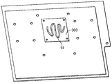
일 실시예에 있어서, 열 인터페이스 재료(14)는 비아(12)의 표면, 제 1 금속 재료(200)의 일부분, 및 제 1 금속 재료(200)의 금속 핀 또는 전도냉각식 히트프레임 부분에 도포된다. 하나 이상의 금속 재료가 사용될 때, 예를 들면 열 스페이서(300) 및 제 3 금속 재료가 사용될 때, 열 인터페이스 재료(14)는 제 1 금속 재료(200)의 표면과 제 3 금속 재료의 비아 사이에 도포된다.In one embodiment,
열 인터페이스 재료는 제 1 금속 재료(200) 및 열 스페이서(300)의 표면 마무리내의 결함을 충전하여, 보다 낮은 열 임피던스를 갖는 열 인터페이스를 생성한다. 일 실시예에 있어서, 도 2에 도시된 바와 같이, 열 인터페이스 재료(14)는 미국 미네소타주 챈하센에 소재하는 버그퀴스트(Bergquist)로부터 시중에서 입수가능한 TIC-4000이다.The thermal interface material fills the defects in the surface finish of the
이제 도 3을 참조하면, 히트싱크(500)를 형성하기 위해서, 제 1 금속 재료(200)내의 비아(12), 열 스페이서(300)(사용될 경우 그리고 도 3에 도시되지 않음), 제 3 금속 재료(사용될 경우 그리고 도 3에 도시되지 않음)내의 비아 및 TPG(100)(도 3에 도시되지 않음)는 함께 접착된다. 적절하게, 도 1 내지 도 3을 종합적으로 참조하면, 비아(12), 열 스페이서(300) 및 TPG(100)는 접착되어, 열 스페이서(300)를 통해 열 공급원 요소(도시하지 않음)로부터 TPG 요소(100)까지 그리고 다음에 TPG 요소(100)의 구멍(10)을 통해서 제 1 금속 재료(200)내의 비아(12)까지, 다음에 외측 환경까지의 열을 전도하는 것을 촉진하도록 구성된 히트싱크(500)를 형성한다.Referring now to FIG. 3, to form a
일 실시예에 있어서, 부품들은 적당한 전기도금을 이용하여 접착된다. 본 기술 분야에 공지된 모든 적당한 전기도금 프로세스는 본 발명의 방법으로 이용될 수 있다. 일반적으로, 본 기술 분야에 공지된 바와 같이 애노드 단부, 대향 캐소드 단부 및 애노드 단부와 캐소드 단부 사이의 비전도성 하우징을 포함하는 전해 장치가 전기도금 프로세스용으로 이용된다. 전해 장치의 하우징은 전해액을 포함한다. 일 실시예에 있어서, 프로세스는 TPG(100), 제 1 금속 재료(200), 열 스페이서(300)(사용될 경우) 및 제 3 금속 재료(사용될 경우)를 전해액과 동시에 접촉시키는 단계를 포함한다. 전형적으로, 도금은 존재할 수 있는 모든 보이드를 충전하도록 층을 형성하기 위해 다중 반복으로 부착된다. 보다 상세하게, 일단 TPG 요소(100), 제 1 금속 재료(200), 열 스페이서(300) 및 제 3 금속 재료가 전해액과 접촉되면, 전해 장치의 애노드 단부와 캐소드 단부 사이에 전류를 통과시킴으로써 전기도금이 실행된다.In one embodiment, the parts are glued using suitable electroplating. All suitable electroplating processes known in the art can be used with the method of the present invention. In general, electrolytic devices including an anode end, an opposing cathode end and a nonconductive housing between the anode end and the cathode end as known in the art are used for the electroplating process. The housing of the electrolytic device includes an electrolyte solution. In one embodiment, the process includes simultaneously contacting the
변형 실시예에 있어서, TPG 요소(100), 제 1 금속 재료(200), 열 스페이서(300)(사용될 경우) 및 제 3 금속 재료(사용될 경우)는 납땜 프로세스(도 6 참조)를 이용하여 함께 접착된다. 특정 실시예에 있어서, 이 방법은 제 1 금속 재료(200)(상술한 바와 같이 비아(12)와 조합하여 또는 비아(12)를 구비하지 않고)의 외부 표면상에 적어도 하나의 솔더 볼(도시하지 않음)을 부착시키는 단계를 포함한다. 그러나, 다중 솔더 볼은 전형적으로 제 1 금속 재료(200)상에 부착된다. 적절하게, 상술한 바와 같이 비아(12)와 유사하게, 솔더 볼은 TPG 요소(100)의 구멍(10)을 충전하도록 구성되어, 열 스페이서(300)(사용될 경우 그리고 도 6에는 도시되지 않음) 둘레의 모든 갭을 충전하고 그리고 제 1 금속 재료(200) 및 열 스페이서(300)(사용될 경우)를 종래의 납땜 메카니즘을 이용하여 TPG 요소(100)에 결합한다. 다른 특정 실시예에 있어서, 솔더(600)는 비아(12), 열 스페이서(300)(사용될 경우, 도 6에는 도시되지 않음) 및 TPG 요소(100) 사이의 인터페이스에 도포된다. 솔더가 도포되는 방법과 상관없이, 사전부착된 솔더 볼 또는 외부에 도포된 솔더(600)를 통해서, 솔더는 가열되어 용융되게 하며, 동시에 제 1 금속 재료(200)(그리고 열 스페이서(300) 및 제 3 금속 재료, 사용되는 경우 그리고 도 6에는 도시되지 않음)와 TPG 요소(100) 사이의 충전 갭은 함께 가압되어 용융된 솔더 볼이 TPG 요소(100)의 구멍(10) 및 갭을 통해 유동하고 이들을 충전한다. 솔더(600)가 용융되는 온도는 솔더(600)에 사용된 재료에 따라 다양할 것이지만, 전형적으로 솔더(600)는 약 185℃ 또는 그 이상의 온도로 가열된다. 일단 냉각되면, 솔더(600)는 TPG 요소(100) 둘에서 응고 및 부착될 것이다. 설명한 바와 같이 동시에 전도되는 동안에, 제 1 금속 재료(200) 및 열 스페이서(300)(도시하지 않음)(그리고 사용되는 경우 제 3 금속 재료) 및 TPG 요소(100)는 본 발명의 영역을 벗어남이 없이 함께 가압되고 다음에 가열될 수 있으며, 반대로 가열되고 가압될 수 있다는 것은 본 기술 분야에 숙련된 자들에게는 자명하다.In a variant embodiment, the
적당한 솔더는 납/주석 합금, 납이 첨가되지 않은 주석 합금, 주석/은 합금, 주석/은/구리 합금 및 주석/은/구리/안티몬 합금을 포함하는 재료로 제조될 수 있지만, 이들로 제한되지 않는다. 일 실시예에 있어서, 솔더 페이스트는, 제 1 금속 재료(200)(그리고 사용되는 경우 열 스페이서(300) 및 열 금속 재료)에 도포되는 겔중에 떠도는 납/주석 합금의 입자를 함유한다. 열이 가해져서 비전도성 겔을 용융시키며, 솔더(600)가 용융되어 TPG 요소(100)를 제 1 금속 재료(200)에 접착시킨다.Suitable solders may be made of materials including, but not limited to, lead / tin alloys, lead-free tin alloys, tin / silver alloys, tin / silver / copper alloys, and tin / silver / copper / antimony alloys. Do not. In one embodiment, the solder paste contains particles of lead / tin alloy that float in the gel applied to the first metal material 200 (and the
다른 실시예에 있어서, 본 발명의 방법은 열적으로 전도성 접착제를 이용하여 TPG 요소(100),제 1 금속 재료(200) 및 열 스페이서(300)를 접착하는 단계를 포함한다. 전형적으로, 접착제는 TPG 요소(100), 제 1 금속 재료(200), 열 스페이서(300) 및 제 3 금속 재료중 적어도 하나에 도포된다. 보다 상세하게, 접착제는 본 기술 분야에 공지된 모든 방법을 이용하여 페이스트, 또는 겔형 형태와 같은 반고체 상태로 도포되는 것이 일반적이다.In another embodiment, the method includes bonding the
일 실시예에 있어서, 열 전도성 접착제는 미국 캘리포니아주 비살리아에 소재하는 아르틱 실버 인크(Arctic Silver, Inc.)로부터 시중에서 입수가능한 "Arctic Silver Epoxy"이다. 사용된 접착제의 양은 특정 히트싱크 구성에 따라 통상적으로 좌우될 것이다. 일 실시예에 있어서, 접착제의 대략 1.5mL가 주사기 및 주걱을 이용하여 도포되어, 접착제를 TPG 요소(100), 제 1 금속 재료(200) 및 열 스페이서(300)상에 얇은 층으로 분산된다.In one embodiment, the thermally conductive adhesive is "Arctic Silver Epoxy" commercially available from Arctic Silver, Inc., Visalia, CA. The amount of adhesive used will typically depend on the particular heatsink configuration. In one embodiment, approximately 1.5 mL of the adhesive is applied using a syringe and spatula to disperse the adhesive in a thin layer on the
일 실시예에 있어서, 히트싱크는 미국 미네소타주 챈하센에 소재하는 버그퀴스트(Bergquist)로부터 시중에서 입수가능한 TIC400 열 그리스를 이용하여 열 공급원 요소에 도포된다.In one embodiment, the heatsink is applied to the heat source element using commercially available TIC400 thermal grease from Bergquist, Chanhasen, Minnesota, USA.
상술한 바와 같이, 접착을 위한 상술한 방법(예를 들면, 전기도금 프로세스, 납땜 프로세스 및 접착제)은 따로따로 설명되었지만, 3개의 접착 방법의 모든 조합이 본 발명의 영역을 벗어남이 없이 히트싱크를 형성하기 위해 조합으로 사용될 수 있다는 것을 이해해야 한다.As mentioned above, the aforementioned methods for adhesion (e.g., electroplating processes, soldering processes, and adhesives) have been described separately, but all combinations of the three bonding methods can be used to heat sinks without departing from the scope of the present invention. It should be understood that it can be used in combination to form.
본 발명이 다양한 특정 실시예에 관하여 설명되었지만, 본 기술분야에 숙련된 자는 본 발명이 특허청구범위의 사상 및 범위내에서 변형이 이루어질 수 있다는 것을 인식할 것이다.Although the present invention has been described with respect to various specific embodiments, those skilled in the art will recognize that the present invention may be modified within the spirit and scope of the claims.
Claims (26)
열분해 흑연(thermo pyrolytic graphite; TPG) 요소를 통해 적어도 하나의 구멍을 형성하는 단계와,
제 1 금속 재료내에 적어도 하나의 비아를 형성하는 단계로서, 적어도 하나의 비아의 각 비아는 상기 적어도 하나의 구멍중 대응하는 구멍내에 위치되도록 구성되어 있는, 상기 적어도 하나의 비아 형성 단계와,
제 2 금속 재료로 제조된 열 스페이서를 제공하는 단계로서, 상기 열 스페이서는 열 공급원 요소를 수용하도록 구성되어 있는, 상기 열 스페이서 제공 단계와,
상기 TPG 요소의 외부 표면에 금속계 코팅을 도포하는 단계와,
상기 적어도 하나의 비아 및 상기 열 스페이서를 상기 TPG 요소의 도포된 외부 표면에 접착하는 단계로서, 상기 열 스페이서 및 상기 TPG 요소는 상기 히트싱크를 형성하도록 접착되어, 상기 열 스페이서를 통해 상기 열 공급원 요소로부터 각 비아까지 그리고 대응하는 구멍을 통해서 열을 전도시키는 것을 촉진하는, 상기 접착 단계를 포함하는
히트싱크 형성 방법.In the method of forming a heat sink,
Forming at least one hole through a pyrolytic graphite (TPG) element,
Forming at least one via in the first metallic material, wherein each via of the at least one via is configured to be positioned in a corresponding one of the at least one aperture;
Providing a thermal spacer made of a second metal material, the thermal spacer configured to receive a heat source element;
Applying a metallic coating to the outer surface of the TPG element;
Adhering the at least one via and the thermal spacer to an applied outer surface of the TPG element, wherein the thermal spacer and the TPG element are bonded to form the heatsink and through the thermal spacer the heat source element To the respective vias and through the corresponding holes to facilitate conducting heat.
Heat sink formation method.
상기 적어도 하나의 구멍을 평면 TPG 요소를 통해 형성하는 단계를 더 포함하는
히트싱크 형성 방법.The method of claim 1,
Further forming the at least one hole through a planar TPG element
Heat sink formation method.
적어도 하나의 구멍을 형성하는 상기 단계가 상기 TPG 요소를 통해 복수의 구멍을 형성하는 단계를 포함하며, 상기 복수의 구멍은 원형, 타원형, 정사각형, 직사각형 및 삼각형중 하나로 형성되는
히트싱크 형성 방법.The method of claim 1,
The step of forming at least one hole comprises forming a plurality of holes through the TPG element, the plurality of holes being formed into one of a circle, an ellipse, a square, a rectangle and a triangle.
Heat sink formation method.
상기 제 1 금속 재료에 복수의 비아를 형성하는 단계를 더 포함하는
히트싱크 형성 방법.The method of claim 1,
Forming a plurality of vias in the first metal material
Heat sink formation method.
상기 복수의 비아는 서로 독립적인 비아인
히트싱크 형성 방법.The method of claim 4, wherein
The plurality of vias are vias independent of each other.
Heat sink formation method.
상기 적어도 하나의 비아는 알루미늄, 구리, 인듐 및 이들의 조합물로 구성되는 그룹으로부터 선택되는 제 1 금속 재료로 형성되는
히트싱크 형성 방법.The method of claim 1,
The at least one via is formed of a first metal material selected from the group consisting of aluminum, copper, indium and combinations thereof
Heat sink formation method.
상기 적어도 하나의 비아는 금속 핀 조립체(metal fin assembly)에 형성되는
히트싱크 형성 방법.The method according to claim 6,
The at least one via is formed in a metal fin assembly
Heat sink formation method.
상기 적어도 하나의 비아는 전도냉각식 히트프레임에 형성되는
히트싱크 형성 방법.The method according to claim 6,
The at least one via is formed in a conductively cooled heat frame.
Heat sink formation method.
상기 열 스페이서는 알루미늄, 구리, 인듐 및 이들의 조합물로 구성되는 그룹으로부터 선택되는 제 2 금속 재료에 마련되는
히트싱크 형성 방법.The method of claim 1,
The thermal spacer is provided on a second metal material selected from the group consisting of aluminum, copper, indium and combinations thereof.
Heat sink formation method.
구리-니켈 코팅 재료가 상기 TPG 요소의 외부 표면에 도포되는
히트싱크 형성 방법.The method of claim 1,
Copper-nickel coating material is applied to the outer surface of the TPG element
Heat sink formation method.
상기 적어도 하나의 비아 및 상기 열 스페이서는 열 전도성 접착제를 이용하여 상기 TPG 요소의 코팅된 외부 표면에 접착되는
히트싱크 형성 방법.The method of claim 1,
The at least one via and the thermal spacer are bonded to the coated outer surface of the TPG element using a thermally conductive adhesive.
Heat sink formation method.
상기 적어도 하나의 비아 및 상기 열 스페이서는 솔더를 이용하여 상기 TPG 요소의 코팅된 외부 표면에 접착되는
히트싱크 형성 방법.The method of claim 1,
The at least one via and the thermal spacer are bonded to the coated outer surface of the TPG element using solder.
Heat sink formation method.
열분해 흑연(TPG) 요소를 통해 적어도 하나의 구멍을 형성하는 단계와,
제 1 금속 재료내에 적어도 하나의 비아를 형성하는 단계로서, 적어도 하나의 비아의 각 비아는 상기 적어도 하나의 구멍중 대응하는 구멍내에 위치되도록 구성되어 있는, 상기 적어도 하나의 비아 형성 단계와,
제 2 금속 재료로 제조된 열 스페이서를 제공하는 단계로서, 상기 열 스페이서는 열 공급원 요소를 수용하도록 구성되어 있는, 상기 열 스페이서 제공 단계와,
전기도금 프로세스를 이용하여 상기 TPG 요소에 각 비아 및 상기 열 스페이서를 접착하는 단계로서, 각 비아, 상기 열 스페이서 및 상기 TPG 요소는 상기 히트싱크를 형성하도록 접착되어, 상기 열 스페이서를 통해 상기 열 공급원 요소로부터 각 비아까지 그리고 대응하는 구멍을 통해서 열을 전도시키는 것을 촉진하도록 구성된, 상기 접착 단계를 포함하는
히트싱크 형성 방법.In the method of forming a heat sink,
Forming at least one hole through a pyrolytic graphite (TPG) element,
Forming at least one via in the first metallic material, wherein each via of the at least one via is configured to be positioned in a corresponding one of the at least one aperture;
Providing a thermal spacer made of a second metal material, the thermal spacer configured to receive a heat source element;
Adhering each via and the thermal spacer to the TPG element using an electroplating process, wherein each via, the thermal spacer and the TPG element are glued to form the heat sink, thereby providing the heat source through the thermal spacer. Comprising the bonding step, configured to facilitate conducting heat from the element to each via and through the corresponding hole.
Heat sink formation method.
적어도 하나의 구멍을 형성하는 상기 단계가 상기 TPG 요소를 통해 복수의 구멍을 형성하는 단계를 포함하며, 상기 복수의 구멍은 원형, 타원형, 정사각형, 직사각형 및 삼각형중 하나로 형성되는
히트싱크 형성 방법.The method of claim 13,
The step of forming at least one hole comprises forming a plurality of holes through the TPG element, the plurality of holes being formed into one of a circle, an ellipse, a square, a rectangle and a triangle.
Heat sink formation method.
상기 제 1 금속 재료에 복수의 비아를 형성하는 단계를 더 포함하는
히트싱크 형성 방법.The method of claim 13,
Forming a plurality of vias in the first metal material
Heat sink formation method.
상기 적어도 하나의 비아는 알루미늄, 구리, 인듐 및 이들의 조합물로 구성되는 그룹으로부터 선택되는 제 1 금속 재료로 형성되는
히트싱크 형성 방법.The method of claim 13,
The at least one via is formed of a first metal material selected from the group consisting of aluminum, copper, indium and combinations thereof
Heat sink formation method.
상기 적어도 하나의 비아는 금속 핀 조립체에 형성되는
히트싱크 형성 방법.17. The method of claim 16,
The at least one via is formed in the metal pin assembly
Heat sink formation method.
상기 열 스페이서는 알루미늄, 구리, 인듐 및 이들의 조합물로 구성되는 그룹으로부터 선택되는 제 1 금속 재료에 마련되는
히트싱크 형성 방법.17. The method of claim 16,
The thermal spacer is provided on a first metal material selected from the group consisting of aluminum, copper, indium and combinations thereof.
Heat sink formation method.
상기 제 1 금속 재료의 비아의 외부 표면과 상기 제 1 금속 재료의 상기 금속 핀 조립체 사이에 열 인터페이스를 가하는 단계를 더 포함하는
히트싱크 형성 방법.The method of claim 17,
Applying a thermal interface between an outer surface of the via of the first metal material and the metal pin assembly of the first metal material;
Heat sink formation method.
열분해 흑연(TPG) 요소를 통해 적어도 하나의 구멍을 형성하는 단계와,
상기 TPG 요소의 외부 표면에 금속계 코팅을 도포하는 단계와,
제 1 금속 재료의 외부 표면에 적어도 하나의 솔더 볼을 부착시키는 단계로서, 상기 적어도 하나의 솔더 볼은 상기 적어도 하나의 구멍의 대응하는 구멍을 충전하도록 구성된, 상기 부착 단계와,
상기 솔더 볼이 상기 대응하는 구멍을 실질적으로 충전하도록, 상기 제 1 금속 재료를 상기 TPG 요소에 가압하는 단계와,
상기 제 1 금속 재료를 상기 TPG 요소에 납땜하도록 상기 제 1 금속 재료를 가열하는 단계를 포함하는
히트싱크 형성 방법.In the method of forming a heat sink,
Forming at least one hole through a pyrolytic graphite (TPG) element,
Applying a metallic coating to the outer surface of the TPG element;
Attaching at least one solder ball to an outer surface of a first metal material, the at least one solder ball configured to fill a corresponding hole of the at least one hole;
Pressing the first metal material to the TPG element such that the solder ball substantially fills the corresponding hole;
Heating the first metal material to solder the first metal material to the TPG element.
Heat sink formation method.
적어도 하나의 구멍을 형성하는 상기 단계가 상기 TPG 요소를 통해 복수의 구멍을 형성하는 단계를 포함하며, 상기 복수의 구멍은 원형, 타원형, 정사각형, 직사각형 및 삼각형중 하나로 형성되는
히트싱크 형성 방법.The method of claim 20,
The step of forming at least one hole comprises forming a plurality of holes through the TPG element, the plurality of holes being formed into one of a circle, an ellipse, a square, a rectangle and a triangle.
Heat sink formation method.
상기 적어도 하나의 솔더 볼을 부착시키는 상기 단계가 상기 제 1 금속 재료의 외부 표면에 복수의 솔더 볼을 부착시키는 단계를 포함하는
히트싱크 형성 방법.The method of claim 20,
Attaching the at least one solder ball includes attaching a plurality of solder balls to an outer surface of the first metal material.
Heat sink formation method.
상기 적어도 하나의 솔더 볼은 알루미늄, 구리, 인듐 및 이들의 조합물로 구성되는 그룹으로부터 선택되는 상기 제 1 금속 재료의 외부 표면상에 부착되는
히트싱크 형성 방법.The method of claim 20,
The at least one solder ball is attached onto an outer surface of the first metal material selected from the group consisting of aluminum, copper, indium and combinations thereof.
Heat sink formation method.
제 1 금속 재료의 외부 표면에 적어도 하나의 솔더 볼을 부착시키는 상기 단계가 알루미늄, 구리, 인듐 및 이들의 조합물로부터 선택된 적어도 하나의 솔더 볼을 상기 제 1 금속 재료의 외부 표면에 부착시키는 단계를 포함하는
히트싱크 형성 방법.The method of claim 20,
Attaching the at least one solder ball to the outer surface of the first metal material comprises attaching the at least one solder ball selected from aluminum, copper, indium and combinations thereof to the outer surface of the first metal material. Containing
Heat sink formation method.
금속계 코팅을 상기 TPG 요소의 외부 표면에 도포하는 상기 단계가 구리-니켈 코팅 재료를 상기 TPG 요소의 외부 표면에 도포하는 단계를 포함하는
히트싱크 형성 방법.The method of claim 20,
The step of applying a metallic coating to the outer surface of the TPG element comprises applying a copper-nickel coating material to the outer surface of the TPG element.
Heat sink formation method.
상기 제 1 금속 재료의 외부 표면과 상기 TPG 요소의 외부 표면 사이에 열 인터페이스 재료를 도포하는 단계를 더 포함하는
히트싱크 형성 방법.The method of claim 20,
Applying a thermal interface material between the outer surface of the first metal material and the outer surface of the TPG element;
Heat sink formation method.
Applications Claiming Priority (2)
| Application Number | Priority Date | Filing Date | Title |
|---|---|---|---|
| US11/967,298 US20090165302A1 (en) | 2007-12-31 | 2007-12-31 | Method of forming a heatsink |
| US11/967,298 | 2007-12-31 |
Publications (1)
| Publication Number | Publication Date |
|---|---|
| KR20100126284A true KR20100126284A (en) | 2010-12-01 |
Family
ID=40419402
Family Applications (1)
| Application Number | Title | Priority Date | Filing Date |
|---|---|---|---|
| KR1020107016985A KR20100126284A (en) | 2007-12-31 | 2008-12-08 | Method of forming a heatsink |
Country Status (6)
| Country | Link |
|---|---|
| US (1) | US20090165302A1 (en) |
| EP (1) | EP2238816A1 (en) |
| JP (1) | JP5469089B2 (en) |
| KR (1) | KR20100126284A (en) |
| CN (1) | CN101953240B (en) |
| WO (1) | WO2009088603A1 (en) |
Families Citing this family (6)
| Publication number | Priority date | Publication date | Assignee | Title |
|---|---|---|---|---|
| US8347502B2 (en) * | 2007-12-28 | 2013-01-08 | Ge Intelligent Platforms, Inc. | Heat sink and method of forming a heatsink using a wedge-lock system |
| US8957316B2 (en) * | 2010-09-10 | 2015-02-17 | Honeywell International Inc. | Electrical component assembly for thermal transfer |
| JP5704994B2 (en) * | 2011-03-31 | 2015-04-22 | インターナショナル・ビジネス・マシーンズ・コーポレーションInternational Business Machines Corporation | Semiconductor bonding equipment |
| US9064852B1 (en) * | 2011-12-05 | 2015-06-23 | The Peregrine Falcon Corporation | Thermal pyrolytic graphite enhanced components |
| EP3410478A1 (en) * | 2017-05-29 | 2018-12-05 | Mitsubishi Electric R & D Centre Europe B.V. | Power module and method for manufacturing the power module |
| CN111587210A (en) * | 2017-12-29 | 2020-08-25 | 空中客车防务和空间公司 | High conductivity heat connector |
Family Cites Families (11)
| Publication number | Priority date | Publication date | Assignee | Title |
|---|---|---|---|---|
| AU697409B2 (en) * | 1995-01-25 | 1998-10-08 | Nortel Networks Corporation | Printed circuit board and heat sink arrangement |
| JP4051402B2 (en) * | 1997-09-19 | 2008-02-27 | モーメンティブ・パフォーマンス・マテリアルズ・インク | Flexible heat transfer device and method for manufacturing the same |
| US6131651A (en) * | 1998-09-16 | 2000-10-17 | Advanced Ceramics Corporation | Flexible heat transfer device and method |
| WO1999014805A1 (en) * | 1997-09-19 | 1999-03-25 | Advanced Ceramics Corporation | Flexible heat transfer device and method |
| JP2003060141A (en) * | 2001-08-20 | 2003-02-28 | Otsuka Denki Kk | Super heat conductor and cooling unit using the same |
| US6758263B2 (en) * | 2001-12-13 | 2004-07-06 | Advanced Energy Technology Inc. | Heat dissipating component using high conducting inserts |
| JP2003188323A (en) * | 2001-12-19 | 2003-07-04 | Sony Corp | Graphite sheet and its manufacturing method |
| US6907917B2 (en) * | 2003-01-10 | 2005-06-21 | International Business Machines Corporation | Graphite-based heat sinks and method and apparatus for the manufacture thereof |
| JP2005210035A (en) * | 2004-01-26 | 2005-08-04 | Otsuka Denki Kk | Graphite composite material |
| US7889502B1 (en) * | 2005-11-04 | 2011-02-15 | Graftech International Holdings Inc. | Heat spreading circuit assembly |
| US7303005B2 (en) * | 2005-11-04 | 2007-12-04 | Graftech International Holdings Inc. | Heat spreaders with vias |
-
2007
- 2007-12-31 US US11/967,298 patent/US20090165302A1/en not_active Abandoned
-
2008
- 2008-12-08 EP EP08869712A patent/EP2238816A1/en not_active Withdrawn
- 2008-12-08 WO PCT/US2008/085783 patent/WO2009088603A1/en active Application Filing
- 2008-12-08 CN CN200880124099.9A patent/CN101953240B/en not_active Expired - Fee Related
- 2008-12-08 JP JP2010540731A patent/JP5469089B2/en not_active Expired - Fee Related
- 2008-12-08 KR KR1020107016985A patent/KR20100126284A/en not_active Application Discontinuation
Also Published As
| Publication number | Publication date |
|---|---|
| WO2009088603A1 (en) | 2009-07-16 |
| CN101953240A (en) | 2011-01-19 |
| JP2011508449A (en) | 2011-03-10 |
| CN101953240B (en) | 2014-01-29 |
| JP5469089B2 (en) | 2014-04-09 |
| US20090165302A1 (en) | 2009-07-02 |
| EP2238816A1 (en) | 2010-10-13 |
Similar Documents
| Publication | Publication Date | Title |
|---|---|---|
| US7119432B2 (en) | Method and apparatus for establishing improved thermal communication between a die and a heatspreader in a semiconductor package | |
| US6523608B1 (en) | Thermal interface material on a mesh carrier | |
| JP4159861B2 (en) | Method for manufacturing heat dissipation structure of printed circuit board | |
| US8647752B2 (en) | Thermal interface material assemblies, and related methods | |
| TWI326922B (en) | ||
| EP2750490B1 (en) | Component-mounting printed circuit board and manufacturing method for same | |
| KR20100126284A (en) | Method of forming a heatsink | |
| JPS6094749A (en) | Ic-chip cooling device | |
| JPS596565A (en) | Heat conductive structure | |
| JP2008244473A (en) | Flexible electronic circuit package with stand-off and method for manufacturing the same | |
| JP2006024755A (en) | Circuit board | |
| TW200526098A (en) | Electrical circuit apparatus and method for assembling same | |
| JP6492768B2 (en) | Electronic device and solder mounting method | |
| JP4407509B2 (en) | Insulated heat transfer structure and power module substrate | |
| JP6477105B2 (en) | Semiconductor device | |
| JP2006269572A (en) | Thermoelectric conversion module, and method of manufacturing the same and circuit substrate | |
| KR101735439B1 (en) | Manufacturing method for radiant heat circuit board | |
| JP3512691B2 (en) | Thermoelectric element and method of manufacturing the same | |
| US20120122278A1 (en) | Method Of Manufacturing Semiconductor Package Board | |
| CN111201621B (en) | Thermoelectric module | |
| JP2018509771A (en) | Electronic chip devices with improved thermal resistance and associated manufacturing processes | |
| JP4876612B2 (en) | Insulated heat transfer structure and power module substrate | |
| JP3669981B2 (en) | Method for manufacturing module structure | |
| KR20130127712A (en) | Skeleton type thermoelectric module and manufacture method thereof and thermoelectric unit having skeleton type thermoelectric module and manufacture method thereof | |
| JP5750101B2 (en) | connector |
Legal Events
| Date | Code | Title | Description |
|---|---|---|---|
| A201 | Request for examination | ||
| E902 | Notification of reason for refusal | ||
| E601 | Decision to refuse application |