KR20100084164A - Method for integrating nvm circuitry with logic circuitry - Google Patents
Method for integrating nvm circuitry with logic circuitry Download PDFInfo
- Publication number
- KR20100084164A KR20100084164A KR1020107009304A KR20107009304A KR20100084164A KR 20100084164 A KR20100084164 A KR 20100084164A KR 1020107009304 A KR1020107009304 A KR 1020107009304A KR 20107009304 A KR20107009304 A KR 20107009304A KR 20100084164 A KR20100084164 A KR 20100084164A
- Authority
- KR
- South Korea
- Prior art keywords
- region
- layer
- sacrificial layers
- logic
- gate
- Prior art date
Links
- 238000000034 method Methods 0.000 title claims abstract description 74
- 239000000463 material Substances 0.000 claims abstract description 57
- 239000000758 substrate Substances 0.000 claims abstract description 28
- 150000004767 nitrides Chemical class 0.000 claims abstract description 19
- 239000006117 anti-reflective coating Substances 0.000 claims description 43
- 238000005498 polishing Methods 0.000 claims description 40
- 239000007772 electrode material Substances 0.000 claims description 18
- 238000002955 isolation Methods 0.000 claims description 15
- 238000005530 etching Methods 0.000 claims description 13
- IJGRMHOSHXDMSA-UHFFFAOYSA-N Atomic nitrogen Chemical compound N#N IJGRMHOSHXDMSA-UHFFFAOYSA-N 0.000 claims description 12
- 238000000059 patterning Methods 0.000 claims description 8
- 229910021420 polycrystalline silicon Inorganic materials 0.000 claims description 8
- 229920005591 polysilicon Polymers 0.000 claims description 8
- 230000015572 biosynthetic process Effects 0.000 claims description 6
- 229910052757 nitrogen Inorganic materials 0.000 claims description 6
- 230000006870 function Effects 0.000 claims description 5
- 238000000206 photolithography Methods 0.000 claims description 4
- 238000012545 processing Methods 0.000 claims description 4
- QVGXLLKOCUKJST-UHFFFAOYSA-N atomic oxygen Chemical compound [O] QVGXLLKOCUKJST-UHFFFAOYSA-N 0.000 claims description 3
- 239000001301 oxygen Substances 0.000 claims description 3
- 229910052760 oxygen Inorganic materials 0.000 claims description 3
- 239000000126 substance Substances 0.000 claims description 3
- 238000003486 chemical etching Methods 0.000 claims description 2
- 238000000926 separation method Methods 0.000 claims description 2
- 238000000151 deposition Methods 0.000 abstract description 14
- 239000004065 semiconductor Substances 0.000 description 28
- 229920002120 photoresistant polymer Polymers 0.000 description 22
- 238000003860 storage Methods 0.000 description 14
- 230000008901 benefit Effects 0.000 description 6
- 238000005229 chemical vapour deposition Methods 0.000 description 6
- 230000000694 effects Effects 0.000 description 5
- 229910052581 Si3N4 Inorganic materials 0.000 description 4
- 230000008021 deposition Effects 0.000 description 4
- 238000013461 design Methods 0.000 description 4
- 238000001312 dry etching Methods 0.000 description 4
- 238000004518 low pressure chemical vapour deposition Methods 0.000 description 4
- 238000000623 plasma-assisted chemical vapour deposition Methods 0.000 description 4
- 238000001039 wet etching Methods 0.000 description 4
- VYPSYNLAJGMNEJ-UHFFFAOYSA-N Silicium dioxide Chemical compound O=[Si]=O VYPSYNLAJGMNEJ-UHFFFAOYSA-N 0.000 description 3
- XUIMIQQOPSSXEZ-UHFFFAOYSA-N Silicon Chemical compound [Si] XUIMIQQOPSSXEZ-UHFFFAOYSA-N 0.000 description 3
- 238000005516 engineering process Methods 0.000 description 3
- 230000010354 integration Effects 0.000 description 3
- 239000002159 nanocrystal Substances 0.000 description 3
- 229910052710 silicon Inorganic materials 0.000 description 3
- 239000010703 silicon Substances 0.000 description 3
- HQVNEWCFYHHQES-UHFFFAOYSA-N silicon nitride Chemical compound N12[Si]34N5[Si]62N3[Si]51N64 HQVNEWCFYHHQES-UHFFFAOYSA-N 0.000 description 3
- GWEVSGVZZGPLCZ-UHFFFAOYSA-N Titan oxide Chemical compound O=[Ti]=O GWEVSGVZZGPLCZ-UHFFFAOYSA-N 0.000 description 2
- 238000013459 approach Methods 0.000 description 2
- 238000000231 atomic layer deposition Methods 0.000 description 2
- 238000004140 cleaning Methods 0.000 description 2
- 238000007796 conventional method Methods 0.000 description 2
- 239000010408 film Substances 0.000 description 2
- 229910052732 germanium Inorganic materials 0.000 description 2
- GNPVGFCGXDBREM-UHFFFAOYSA-N germanium atom Chemical compound [Ge] GNPVGFCGXDBREM-UHFFFAOYSA-N 0.000 description 2
- 238000004519 manufacturing process Methods 0.000 description 2
- 229910052751 metal Inorganic materials 0.000 description 2
- 239000002184 metal Substances 0.000 description 2
- 230000002093 peripheral effect Effects 0.000 description 2
- 238000005240 physical vapour deposition Methods 0.000 description 2
- 229910052814 silicon oxide Inorganic materials 0.000 description 2
- 239000002904 solvent Substances 0.000 description 2
- 125000006850 spacer group Chemical group 0.000 description 2
- 239000010409 thin film Substances 0.000 description 2
- JBRZTFJDHDCESZ-UHFFFAOYSA-N AsGa Chemical compound [As]#[Ga] JBRZTFJDHDCESZ-UHFFFAOYSA-N 0.000 description 1
- 241000252506 Characiformes Species 0.000 description 1
- 229910001218 Gallium arsenide Inorganic materials 0.000 description 1
- 229910004298 SiO 2 Inorganic materials 0.000 description 1
- 229910000577 Silicon-germanium Inorganic materials 0.000 description 1
- ATJFFYVFTNAWJD-UHFFFAOYSA-N Tin Chemical compound [Sn] ATJFFYVFTNAWJD-UHFFFAOYSA-N 0.000 description 1
- MCMNRKCIXSYSNV-UHFFFAOYSA-N ZrO2 Inorganic materials O=[Zr]=O MCMNRKCIXSYSNV-UHFFFAOYSA-N 0.000 description 1
- 239000002253 acid Substances 0.000 description 1
- 150000007513 acids Chemical class 0.000 description 1
- 230000002730 additional effect Effects 0.000 description 1
- 230000004075 alteration Effects 0.000 description 1
- 229910021417 amorphous silicon Inorganic materials 0.000 description 1
- 230000003667 anti-reflective effect Effects 0.000 description 1
- 238000004380 ashing Methods 0.000 description 1
- 239000013078 crystal Substances 0.000 description 1
- 239000003989 dielectric material Substances 0.000 description 1
- 239000003112 inhibitor Substances 0.000 description 1
- 239000012212 insulator Substances 0.000 description 1
- 238000001459 lithography Methods 0.000 description 1
- 239000011159 matrix material Substances 0.000 description 1
- 229910021421 monocrystalline silicon Inorganic materials 0.000 description 1
- -1 oxide Chemical class 0.000 description 1
- TWNQGVIAIRXVLR-UHFFFAOYSA-N oxo(oxoalumanyloxy)alumane Chemical compound O=[Al]O[Al]=O TWNQGVIAIRXVLR-UHFFFAOYSA-N 0.000 description 1
- BPUBBGLMJRNUCC-UHFFFAOYSA-N oxygen(2-);tantalum(5+) Chemical compound [O-2].[O-2].[O-2].[O-2].[O-2].[Ta+5].[Ta+5] BPUBBGLMJRNUCC-UHFFFAOYSA-N 0.000 description 1
- RVTZCBVAJQQJTK-UHFFFAOYSA-N oxygen(2-);zirconium(4+) Chemical compound [O-2].[O-2].[Zr+4] RVTZCBVAJQQJTK-UHFFFAOYSA-N 0.000 description 1
- 235000012239 silicon dioxide Nutrition 0.000 description 1
- 239000000377 silicon dioxide Substances 0.000 description 1
- 238000004528 spin coating Methods 0.000 description 1
- 239000011232 storage material Substances 0.000 description 1
- 229920003002 synthetic resin Polymers 0.000 description 1
- 239000000057 synthetic resin Substances 0.000 description 1
- 229910001936 tantalum oxide Inorganic materials 0.000 description 1
- 239000004408 titanium dioxide Substances 0.000 description 1
Images


Classifications
-
- B—PERFORMING OPERATIONS; TRANSPORTING
- B82—NANOTECHNOLOGY
- B82Y—SPECIFIC USES OR APPLICATIONS OF NANOSTRUCTURES; MEASUREMENT OR ANALYSIS OF NANOSTRUCTURES; MANUFACTURE OR TREATMENT OF NANOSTRUCTURES
- B82Y10/00—Nanotechnology for information processing, storage or transmission, e.g. quantum computing or single electron logic
-
- H—ELECTRICITY
- H01—ELECTRIC ELEMENTS
- H01L—SEMICONDUCTOR DEVICES NOT COVERED BY CLASS H10
- H01L21/00—Processes or apparatus adapted for the manufacture or treatment of semiconductor or solid state devices or of parts thereof
- H01L21/02—Manufacture or treatment of semiconductor devices or of parts thereof
- H01L21/04—Manufacture or treatment of semiconductor devices or of parts thereof the devices having at least one potential-jump barrier or surface barrier, e.g. PN junction, depletion layer or carrier concentration layer
- H01L21/18—Manufacture or treatment of semiconductor devices or of parts thereof the devices having at least one potential-jump barrier or surface barrier, e.g. PN junction, depletion layer or carrier concentration layer the devices having semiconductor bodies comprising elements of Group IV of the Periodic System or AIIIBV compounds with or without impurities, e.g. doping materials
- H01L21/30—Treatment of semiconductor bodies using processes or apparatus not provided for in groups H01L21/20 - H01L21/26
- H01L21/31—Treatment of semiconductor bodies using processes or apparatus not provided for in groups H01L21/20 - H01L21/26 to form insulating layers thereon, e.g. for masking or by using photolithographic techniques; After treatment of these layers; Selection of materials for these layers
- H01L21/3105—After-treatment
- H01L21/31051—Planarisation of the insulating layers
-
- H—ELECTRICITY
- H01—ELECTRIC ELEMENTS
- H01L—SEMICONDUCTOR DEVICES NOT COVERED BY CLASS H10
- H01L29/00—Semiconductor devices adapted for rectifying, amplifying, oscillating or switching, or capacitors or resistors with at least one potential-jump barrier or surface barrier, e.g. PN junction depletion layer or carrier concentration layer; Details of semiconductor bodies or of electrodes thereof ; Multistep manufacturing processes therefor
- H01L29/40—Electrodes ; Multistep manufacturing processes therefor
- H01L29/401—Multistep manufacturing processes
- H01L29/4011—Multistep manufacturing processes for data storage electrodes
- H01L29/40114—Multistep manufacturing processes for data storage electrodes the electrodes comprising a conductor-insulator-conductor-insulator-semiconductor structure
-
- H—ELECTRICITY
- H01—ELECTRIC ELEMENTS
- H01L—SEMICONDUCTOR DEVICES NOT COVERED BY CLASS H10
- H01L29/00—Semiconductor devices adapted for rectifying, amplifying, oscillating or switching, or capacitors or resistors with at least one potential-jump barrier or surface barrier, e.g. PN junction depletion layer or carrier concentration layer; Details of semiconductor bodies or of electrodes thereof ; Multistep manufacturing processes therefor
- H01L29/40—Electrodes ; Multistep manufacturing processes therefor
- H01L29/401—Multistep manufacturing processes
- H01L29/4011—Multistep manufacturing processes for data storage electrodes
- H01L29/40117—Multistep manufacturing processes for data storage electrodes the electrodes comprising a charge-trapping insulator
-
- H—ELECTRICITY
- H01—ELECTRIC ELEMENTS
- H01L—SEMICONDUCTOR DEVICES NOT COVERED BY CLASS H10
- H01L29/00—Semiconductor devices adapted for rectifying, amplifying, oscillating or switching, or capacitors or resistors with at least one potential-jump barrier or surface barrier, e.g. PN junction depletion layer or carrier concentration layer; Details of semiconductor bodies or of electrodes thereof ; Multistep manufacturing processes therefor
- H01L29/40—Electrodes ; Multistep manufacturing processes therefor
- H01L29/41—Electrodes ; Multistep manufacturing processes therefor characterised by their shape, relative sizes or dispositions
- H01L29/423—Electrodes ; Multistep manufacturing processes therefor characterised by their shape, relative sizes or dispositions not carrying the current to be rectified, amplified or switched
- H01L29/42312—Gate electrodes for field effect devices
- H01L29/42316—Gate electrodes for field effect devices for field-effect transistors
- H01L29/4232—Gate electrodes for field effect devices for field-effect transistors with insulated gate
- H01L29/42324—Gate electrodes for transistors with a floating gate
- H01L29/42328—Gate electrodes for transistors with a floating gate with at least one additional gate other than the floating gate and the control gate, e.g. program gate, erase gate or select gate
-
- H—ELECTRICITY
- H01—ELECTRIC ELEMENTS
- H01L—SEMICONDUCTOR DEVICES NOT COVERED BY CLASS H10
- H01L29/00—Semiconductor devices adapted for rectifying, amplifying, oscillating or switching, or capacitors or resistors with at least one potential-jump barrier or surface barrier, e.g. PN junction depletion layer or carrier concentration layer; Details of semiconductor bodies or of electrodes thereof ; Multistep manufacturing processes therefor
- H01L29/40—Electrodes ; Multistep manufacturing processes therefor
- H01L29/41—Electrodes ; Multistep manufacturing processes therefor characterised by their shape, relative sizes or dispositions
- H01L29/423—Electrodes ; Multistep manufacturing processes therefor characterised by their shape, relative sizes or dispositions not carrying the current to be rectified, amplified or switched
- H01L29/42312—Gate electrodes for field effect devices
- H01L29/42316—Gate electrodes for field effect devices for field-effect transistors
- H01L29/4232—Gate electrodes for field effect devices for field-effect transistors with insulated gate
- H01L29/42324—Gate electrodes for transistors with a floating gate
- H01L29/42332—Gate electrodes for transistors with a floating gate with the floating gate formed by two or more non connected parts, e.g. multi-particles flating gate
-
- H—ELECTRICITY
- H01—ELECTRIC ELEMENTS
- H01L—SEMICONDUCTOR DEVICES NOT COVERED BY CLASS H10
- H01L29/00—Semiconductor devices adapted for rectifying, amplifying, oscillating or switching, or capacitors or resistors with at least one potential-jump barrier or surface barrier, e.g. PN junction depletion layer or carrier concentration layer; Details of semiconductor bodies or of electrodes thereof ; Multistep manufacturing processes therefor
- H01L29/40—Electrodes ; Multistep manufacturing processes therefor
- H01L29/41—Electrodes ; Multistep manufacturing processes therefor characterised by their shape, relative sizes or dispositions
- H01L29/423—Electrodes ; Multistep manufacturing processes therefor characterised by their shape, relative sizes or dispositions not carrying the current to be rectified, amplified or switched
- H01L29/42312—Gate electrodes for field effect devices
- H01L29/42316—Gate electrodes for field effect devices for field-effect transistors
- H01L29/4232—Gate electrodes for field effect devices for field-effect transistors with insulated gate
- H01L29/4234—Gate electrodes for transistors with charge trapping gate insulator
- H01L29/42344—Gate electrodes for transistors with charge trapping gate insulator with at least one additional gate, e.g. program gate, erase gate or select gate
-
- H—ELECTRICITY
- H01—ELECTRIC ELEMENTS
- H01L—SEMICONDUCTOR DEVICES NOT COVERED BY CLASS H10
- H01L29/00—Semiconductor devices adapted for rectifying, amplifying, oscillating or switching, or capacitors or resistors with at least one potential-jump barrier or surface barrier, e.g. PN junction depletion layer or carrier concentration layer; Details of semiconductor bodies or of electrodes thereof ; Multistep manufacturing processes therefor
- H01L29/66—Types of semiconductor device ; Multistep manufacturing processes therefor
- H01L29/66007—Multistep manufacturing processes
- H01L29/66075—Multistep manufacturing processes of devices having semiconductor bodies comprising group 14 or group 13/15 materials
- H01L29/66227—Multistep manufacturing processes of devices having semiconductor bodies comprising group 14 or group 13/15 materials the devices being controllable only by the electric current supplied or the electric potential applied, to an electrode which does not carry the current to be rectified, amplified or switched, e.g. three-terminal devices
- H01L29/66409—Unipolar field-effect transistors
- H01L29/66477—Unipolar field-effect transistors with an insulated gate, i.e. MISFET
- H01L29/66825—Unipolar field-effect transistors with an insulated gate, i.e. MISFET with a floating gate
-
- H—ELECTRICITY
- H01—ELECTRIC ELEMENTS
- H01L—SEMICONDUCTOR DEVICES NOT COVERED BY CLASS H10
- H01L29/00—Semiconductor devices adapted for rectifying, amplifying, oscillating or switching, or capacitors or resistors with at least one potential-jump barrier or surface barrier, e.g. PN junction depletion layer or carrier concentration layer; Details of semiconductor bodies or of electrodes thereof ; Multistep manufacturing processes therefor
- H01L29/66—Types of semiconductor device ; Multistep manufacturing processes therefor
- H01L29/66007—Multistep manufacturing processes
- H01L29/66075—Multistep manufacturing processes of devices having semiconductor bodies comprising group 14 or group 13/15 materials
- H01L29/66227—Multistep manufacturing processes of devices having semiconductor bodies comprising group 14 or group 13/15 materials the devices being controllable only by the electric current supplied or the electric potential applied, to an electrode which does not carry the current to be rectified, amplified or switched, e.g. three-terminal devices
- H01L29/66409—Unipolar field-effect transistors
- H01L29/66477—Unipolar field-effect transistors with an insulated gate, i.e. MISFET
- H01L29/66833—Unipolar field-effect transistors with an insulated gate, i.e. MISFET with a charge trapping gate insulator, e.g. MNOS transistors
-
- H—ELECTRICITY
- H01—ELECTRIC ELEMENTS
- H01L—SEMICONDUCTOR DEVICES NOT COVERED BY CLASS H10
- H01L29/00—Semiconductor devices adapted for rectifying, amplifying, oscillating or switching, or capacitors or resistors with at least one potential-jump barrier or surface barrier, e.g. PN junction depletion layer or carrier concentration layer; Details of semiconductor bodies or of electrodes thereof ; Multistep manufacturing processes therefor
- H01L29/66—Types of semiconductor device ; Multistep manufacturing processes therefor
- H01L29/68—Types of semiconductor device ; Multistep manufacturing processes therefor controllable by only the electric current supplied, or only the electric potential applied, to an electrode which does not carry the current to be rectified, amplified or switched
- H01L29/76—Unipolar devices, e.g. field effect transistors
- H01L29/772—Field effect transistors
- H01L29/78—Field effect transistors with field effect produced by an insulated gate
- H01L29/788—Field effect transistors with field effect produced by an insulated gate with floating gate
- H01L29/7881—Programmable transistors with only two possible levels of programmation
-
- H—ELECTRICITY
- H01—ELECTRIC ELEMENTS
- H01L—SEMICONDUCTOR DEVICES NOT COVERED BY CLASS H10
- H01L29/00—Semiconductor devices adapted for rectifying, amplifying, oscillating or switching, or capacitors or resistors with at least one potential-jump barrier or surface barrier, e.g. PN junction depletion layer or carrier concentration layer; Details of semiconductor bodies or of electrodes thereof ; Multistep manufacturing processes therefor
- H01L29/66—Types of semiconductor device ; Multistep manufacturing processes therefor
- H01L29/68—Types of semiconductor device ; Multistep manufacturing processes therefor controllable by only the electric current supplied, or only the electric potential applied, to an electrode which does not carry the current to be rectified, amplified or switched
- H01L29/76—Unipolar devices, e.g. field effect transistors
- H01L29/772—Field effect transistors
- H01L29/78—Field effect transistors with field effect produced by an insulated gate
- H01L29/792—Field effect transistors with field effect produced by an insulated gate with charge trapping gate insulator, e.g. MNOS-memory transistors
-
- H—ELECTRICITY
- H10—SEMICONDUCTOR DEVICES; ELECTRIC SOLID-STATE DEVICES NOT OTHERWISE PROVIDED FOR
- H10B—ELECTRONIC MEMORY DEVICES
- H10B41/00—Electrically erasable-and-programmable ROM [EEPROM] devices comprising floating gates
- H10B41/40—Electrically erasable-and-programmable ROM [EEPROM] devices comprising floating gates characterised by the peripheral circuit region
- H10B41/42—Simultaneous manufacture of periphery and memory cells
- H10B41/43—Simultaneous manufacture of periphery and memory cells comprising only one type of peripheral transistor
- H10B41/44—Simultaneous manufacture of periphery and memory cells comprising only one type of peripheral transistor with a control gate layer also being used as part of the peripheral transistor
-
- H—ELECTRICITY
- H10—SEMICONDUCTOR DEVICES; ELECTRIC SOLID-STATE DEVICES NOT OTHERWISE PROVIDED FOR
- H10B—ELECTRONIC MEMORY DEVICES
- H10B41/00—Electrically erasable-and-programmable ROM [EEPROM] devices comprising floating gates
- H10B41/40—Electrically erasable-and-programmable ROM [EEPROM] devices comprising floating gates characterised by the peripheral circuit region
- H10B41/42—Simultaneous manufacture of periphery and memory cells
- H10B41/43—Simultaneous manufacture of periphery and memory cells comprising only one type of peripheral transistor
- H10B41/48—Simultaneous manufacture of periphery and memory cells comprising only one type of peripheral transistor with a tunnel dielectric layer also being used as part of the peripheral transistor
-
- H—ELECTRICITY
- H10—SEMICONDUCTOR DEVICES; ELECTRIC SOLID-STATE DEVICES NOT OTHERWISE PROVIDED FOR
- H10B—ELECTRONIC MEMORY DEVICES
- H10B43/00—EEPROM devices comprising charge-trapping gate insulators
- H10B43/40—EEPROM devices comprising charge-trapping gate insulators characterised by the peripheral circuit region
Abstract
Description
이 명세서는 일반적으로 집적 회로 제작에 관한 것으로서, 좀더 구체적으로는, 집적 회로 설계를 제작함에 있어서 NVM(Non-Volatile Memory) 회로를 논리 회로와 통합하는 것에 관한 것이다.This specification generally relates to integrated circuit fabrication, and more particularly, to the integration of non-volatile memory (NVM) circuits with logic circuits in fabricating integrated circuit designs.
집적 회로 설계 분야에서는, SoC(System-on-chip) 장치가 흔히 사용된다. "SoC"라는 용어는, 논리(logic), 프로그램 가능 부분들, I/O, 휘발성 메모리 및 비휘발성 메모리를 포함하는, 여러 블록 유형을 단일 집적 회로에 통합하는 장치를 의미한다. In the field of integrated circuit design, system-on-chip (SoC) devices are commonly used. The term "SoC" refers to a device that integrates several block types into a single integrated circuit, including logic, programmable portions, I / O, volatile memory, and nonvolatile memory.
부동-게이트 기반(floating-gate based) 메모리가 SoC 설계에서의 비휘발성 메모리로 흔히 사용된다. SoC에 임베디드되는 부동-게이트 기반 메모리의 스케일링 제한(scaling limitations)을 극복하기 위해, 현재는 TFS(thin film storage) 메모리가 사용되고 있다. TFS 메모리에서, 전하(charge)는 나노크리스탈로 널리 알려진 실리콘 크리스탈로 이루어진 얇은 절연막에 저장된다. Floating-gate based memory is commonly used as nonvolatile memory in SoC designs. To overcome the scaling limitations of floating-gate based memory embedded in SoCs, thin film storage (TFS) memory is currently used. In TFS memory, charge is stored in a thin insulating film made of silicon crystals, commonly known as nanocrystals.
SoC에서의 TFS(Thin Film Semiconductor) 메모리와 논리 회로의 통합은 2개의 게이트 에칭(gate etches)을 요구하는데, 하나는 TFS 영역에서의 선택 게이트를 위한 것이고, 다른 하나는 논리 영역에서의 논리 또는 주변 트랜지스터의 게이트를 위한 것이다. 논리 또는 주변 트랜지스터는 CD(critical dimension)를 가지며 아주 작기 때문에, 패터닝을 복잡하게 한다. 한가지 접근 방법에서는, 게이트 산화물상에 증착되어 트랜지스터의 게이트 치수에 대한 CD 제어를 실현하는 BARC(bottom anti-reflective coating)층을 사용해, 아주 작은 트랜지스터의 게이트가 패터닝된다. BARC는 높은 점도를 가지므로, BARC층은 증착하기가 어렵다. 더 나아가, SoC에서의 메모리 영역과 논리 영역 사이에 높이 차이가 있는 경우, 프로세스는 좀더 복잡해진다. 또한, SoC에서의 메모리 영역과 논리 영역 사이의 물리적 거리가 작으면, 비평면의 아주 두꺼운 BARC층이 논리 영역의 게이트 산화물상에 증착되는데, 이는 에칭하기에 어렵다. 또한, 두꺼운 BARC층은 지나치게 반사 방지적(anti-reflective)이므로, 두꺼운 BARC층을 사용하는 트랜지스터 게이트의 패터닝은 복잡한 프로세스가 된다. 이러한 비평면성 문제를 해결하기 위해서는, 분리 영역이라고 하는, 메모리 영역과 논리 영역 사이의 거리가 커져야 한다. 그러나, 분리 영역 증가는 SoC 설계에서의 레이아웃 비효율성을 수반한다.Integration of thin film semiconductor (TFS) memory and logic circuits in SoCs requires two gate etches, one for select gates in the TFS region and the other for logic or peripherals in the logic region. For the gate of a transistor. Logic or peripheral transistors have a critical dimension (CD) and are very small, which complicates patterning. In one approach, the gate of a very small transistor is patterned using a bottom anti-reflective coating (BARC) layer deposited on the gate oxide to realize CD control over the gate dimensions of the transistor. Since BARC has a high viscosity, BARC layers are difficult to deposit. Furthermore, if there is a height difference between the memory area and the logic area in the SoC, the process becomes more complicated. In addition, if the physical distance between the memory region and the logic region in the SoC is small, a non-planar, very thick BARC layer is deposited on the gate oxide of the logic region, which is difficult to etch. In addition, since the thick BARC layer is too anti-reflective, the patterning of the transistor gate using the thick BARC layer becomes a complicated process. In order to solve this non-planarity problem, the distance between the memory area and the logical area, called an isolation area, must be increased. However, increasing isolation area entails layout inefficiencies in SoC designs.
작은 치수의 트랜지스터를 패터닝하기 위한 다른 접근 방법은 보통의 ARC(anti-reflective coating) 또는 질화물의 증착을 포함한다. 그러나, 비평면성 문제 때문에 이후 프로세스에서 그것을 에칭하기가 어렵다.Another approach for patterning small size transistors involves the deposition of a common anti-reflective coating (ARC) or nitride. However, it is difficult to etch it in subsequent processes because of nonplanarity issues.
SoC에서 NVM 회로와 논리 회로를 통합하면서, 이러한 문제를 극복하고 프로세스 복잡도를 감소시키기 위한 방법이 필요하다.While integrating NVM and logic circuits in SoCs, there is a need for ways to overcome these problems and reduce process complexity.
본 발명의 실시예에서, 방법은 전기적으로 서로 분리되는 제1 정의 영역 및 제2 정의 영역을 가진 기판을 제공한다. 또한, 본 방법은 제1 정의 영역 및 제2 정의 영역 양자에 기판을 덮는(overlying) 제1 게이트 재료층을 제공한다. 더 나아가, 본 방법은 제1 게이트 재료층을 덮는 다중 인접 희생층(multiple adjoining sacrificial layers)을 제공한다. 더 나아가, 본 방법은 다중 인접 희생층을 사용해, 인접한 희생층 중 적어도 하나가 완전히 제거되지 않은 제1 정의 영역에 트랜지스터 제어 전극을 형성한다. 추가적으로, 본 방법은 인접한 희생층 중 하나를 사용해 제2 정의 영역에 트랜지스터 제어 전극을 패터닝한다. 마지막으로, 본 방법은 제1 정의 영역과 제2 정의 영역 모두에서의 트랜지스터 형성을 완료한다.In an embodiment of the invention, the method provides a substrate having a first defining region and a second defining region that are electrically isolated from each other. The method also provides a first gate material layer overlying the substrate in both the first defining region and the second defining region. Furthermore, the method provides multiple adjoining sacrificial layers covering the first gate material layer. Furthermore, the method uses multiple adjacent sacrificial layers to form transistor control electrodes in the first defining region where at least one of the adjacent sacrificial layers is not completely removed. In addition, the method patterns the transistor control electrode in the second defining region using one of the adjacent sacrificial layers. Finally, the method completes transistor formation in both the first and second definition regions.
본 발명의 다른 실시예에서는, 집적 회로 형성 방법이 제공된다. 집적 회로는, 기판상에 형성되고 분리 영역에 의해 분리되는 제1 영역 및 제2 영역을 포함한다. 본 방법은 제1 영역 및 제2 영역 양자에 기판을 덮는 제1 게이트 전극 재료층을 형성하는 단계를 포함한다. 더 나아가, 본 방법은, 제1 영역 및 제2 영역에 어떤 장치를 형성하기에 앞서, 제1 영역 및 제2 영역 양자에 제1 게이트 전극 재료층을 덮는 복수개 희생층을 형성한다. 또한, 본 방법은 복수개 희생층을 사용해 제1 영역에 제1 장치 유형을 형성하는 단계를 포함한다. 더 나아가, 본 방법은 복수개 희생층을 사용해 제2 영역에 제2 장치 유형을 형성하는 단계를 포함한다.In another embodiment of the present invention, an integrated circuit forming method is provided. The integrated circuit includes a first region and a second region formed on a substrate and separated by isolation regions. The method includes forming a first gate electrode material layer covering the substrate in both the first region and the second region. Furthermore, the method forms a plurality of sacrificial layers covering the first gate electrode material layer in both the first and second regions prior to forming any device in the first and second regions. The method also includes forming a first device type in the first region using the plurality of sacrificial layers. Furthermore, the method includes forming a second device type in a second region using a plurality of sacrificial layers.
또 다른 실시예에서도, 집적 회로 형성 방법이 제공된다. 집적 회로는, 기판상에 형성되고 분리 영역에 의해 분리되는 메모리 영역 및 논리 영역을 포함한다. 본 방법은 메모리 영역 및 논리 영역 양자에 기판을 덮는 제1 게이트 전극 재료층을 형성하는 단계를 포함한다. 본 방법은, 메모리 영역 및 논리 영역에 어떤 장치를 형성하기에 앞서, 메모리 영역 및 논리 영역 양자에 제1 게이트 전극 재료층을 덮는 복수개 희생층을 형성하는 단계를 더 포함한다. 또한, 본 방법은 복수개 희생층을 사용해 메모리 영역에 비휘발성 메모리 장치를 형성하는 단계를 포함한다. 또한, 본 방법은 복수개 희생층 중 적어도 하나를 사용해 논리 영역에 논리 장치를 형성하는 단계를 포함한다. 논리 장치를 형성하는데 사용되는 복수개 희생층 중 적어도 하나는 논리 영역에서 논리 장치에 대응하는 게이트 전극을 패터닝하는데 사용되는 ARC(anti-reflective coating)층이다.In yet another embodiment, an integrated circuit forming method is provided. An integrated circuit includes a memory region and a logic region formed on a substrate and separated by isolation regions. The method includes forming a first gate electrode material layer covering a substrate in both a memory region and a logic region. The method further includes forming a plurality of sacrificial layers covering the first gate electrode material layer in both the memory region and the logic region prior to forming any device in the memory region and the logic region. The method also includes forming a nonvolatile memory device in a memory area using a plurality of sacrificial layers. The method also includes forming a logic device in the logic region using at least one of the plurality of sacrificial layers. At least one of the plurality of sacrificial layers used to form the logic device is an anti-reflective coating (ARC) layer used to pattern the gate electrode corresponding to the logic device in the logic region.
본 발명의 바람직한 실시예에 대한 다음의 상세한 설명은 첨부된 도면과 함께 읽을 때 좀더 잘 이해될 것이다. 본 발명은 유사한 참조 번호가 유사한 구성 요소를 지시하는 첨부 도면에 의해 제한되는 것이 아니라 일례로써 설명된다. 도면의 구성 요소는 간략화 및 명료화를 위해 예시되며 반드시 크기대로 예시될 필요는 없다.
도 1은, 본 발명의 실시예에 따른, 기판을 덮는 유전체 재료층 및 게이트 재료층을 갖춘 반도체 장치의 일부의 단면을 예시하고;
도 2는, 본 발명의 실시예에 따른, 다중 인접 희생층을 증착한 이후의 도 1의 반도체 장치를 예시하며;
도 3은, 본 발명의 실시예에 따른, 패터닝된 포토레지스트층을 증착한 이후의 도 2의 반도체 장치를 예시하고;
도 4는, 본 발명의 실시예에 따른, 희생층 및 제1 게이트 재료층을 에칭한 이후의 도 3의 반도체 장치를 예시하며;
도 5는, 본 발명의 실시예에 따른, 희생층상에 전하 저장 스택을 증착한 이후의 도 4의 반도체 장치를 예시하고;
도 6은, 본 발명의 실시예에 따른, 제2 게이트 재료층을 증착한 이후의 도 5의 반도체 장치를 예시하며;
도 7은, 본 발명의 실시예에 따른, 연마 정지층에 이를 때까지 제2 게이트 재료층을 관통하여 연마한 이후의 도 6의 반도체 장치를 예시하고;
도 8 내지 도 11은, 본 발명의 실시예에 따른, 도 7의 반도체 장치의 NVM 영역에서의 선택 게이트 및 제어 게이트의 형성을 예시하며;
도 12는, 본 발명의 실시예에 따른, 논리 영역에서 논리 트랜지스터의 게이트를 패터닝하기 위해 포토레지스트 마스크를 증착한 이후의 도 11의 반도체 장치를 예시하고;
도 13은, 본 발명의 실시예에 따른, 메모리 영역에 메모리 트랜지스터를 그리고 논리 영역에 논리 트랜지스터를 형성하기 위한 최종적인 프로세싱 단계를 예시한다.
당업자라면, 도면의 구성 요소는 간략화 및 명료화를 위해 예시되고 반드시 크기대로 예시될 필요는 없다는 것을 알 수 있을 것이다. 예를 들어, 도면에서의 일부 구성 요소의 치수는 본 발명의 실시예에 대한 이해를 돕기 위해 다른 구성 요소에 비해 과장될 수 있다.The following detailed description of the preferred embodiment of the invention will be better understood when read in conjunction with the accompanying drawings. The invention is illustrated by way of example and not by the accompanying drawings, in which like reference numerals designate like elements. The components in the figures are illustrated for simplicity and clarity and need not necessarily be illustrated to scale.
1 illustrates a cross-section of a portion of a semiconductor device having a dielectric material layer and a gate material layer covering a substrate, in accordance with an embodiment of the present invention;
2 illustrates the semiconductor device of FIG. 1 after depositing multiple adjacent sacrificial layers, in accordance with an embodiment of the invention;
3 illustrates the semiconductor device of FIG. 2 after depositing a patterned photoresist layer, in accordance with an embodiment of the invention;
4 illustrates the semiconductor device of FIG. 3 after etching the sacrificial layer and the first gate material layer, in accordance with an embodiment of the invention;
5 illustrates the semiconductor device of FIG. 4 after depositing a charge storage stack on a sacrificial layer, in accordance with an embodiment of the invention;
6 illustrates the semiconductor device of FIG. 5 after depositing a second gate material layer, in accordance with an embodiment of the invention;
FIG. 7 illustrates the semiconductor device of FIG. 6 after polishing through a second gate material layer until reaching a polishing stop layer, in accordance with an embodiment of the present invention; FIG.
8-11 illustrate the formation of a select gate and a control gate in the NVM region of the semiconductor device of FIG. 7, in accordance with an embodiment of the present invention;
12 illustrates the semiconductor device of FIG. 11 after depositing a photoresist mask to pattern a gate of a logic transistor in a logic region, in accordance with an embodiment of the present invention;
13 illustrates a final processing step for forming a memory transistor in a memory region and a logic transistor in a logic region, in accordance with an embodiment of the invention.
Those skilled in the art will appreciate that the components of the figures are illustrated for simplicity and clarity and need not necessarily be illustrated to scale. For example, the dimensions of some of the components in the figures may be exaggerated relative to other components to facilitate understanding of embodiments of the present invention.
첨부 도면의 상세한 설명은 본 발명의 현재적으로 바람직한 실시예에 대한 설명이고 본 발명이 실시될 수 있는 유일한 형태를 표현하는 것은 아니다. 동일 또는 균등 기능이, 본 발명의 정신 및 범위내에 포함되는 상이한 실시예에 의해 실현될 수도 있다는 것을 이해할 수 있어야 한다.The detailed description of the accompanying drawings is a description of the presently preferred embodiments of the invention and is not intended to represent the only form in which the invention may be practiced. It should be understood that the same or equivalent functions may be realized by different embodiments that fall within the spirit and scope of the invention.
도 1 내지 도 13은, 본 발명의 다양한 실시예에 따른, NVM(Non-Volatile Memory) 회로와 논리 회로를 통합하는 단계 동안의 반도체 웨이퍼의 일부의 단면을 예시한다. 1 through 13 illustrate cross-sectional views of portions of a semiconductor wafer during the step of integrating logic circuits with non-volatile memory (NVM) circuits, in accordance with various embodiments of the present invention.
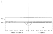
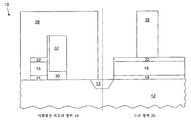
이제 도 1을 참조하면, 본 도면은 집적 회로 다이라고 하는 반도체 장치(10)의 일부의 단면을 예시한다. 반도체 장치(10)는 트렌치 분리(13)에 의해 분리되는 NVM 영역(18) 및 논리 영역(20)을 갖춘 기판(12)을 포함한다. 도 1은 기판(12)을 덮는(overlying) 유전체층(14) 및 제1 게이트 재료층(16)을 나타낸다. 기판(12)은, 갈륨 비화물, 실리콘, 게르마늄, SOI(silicon-on-insulator), 단결정 실리콘, 또는 전자 장치를 형성하는데 통상적으로 사용되는 임의의 다른 재료와 같은, 모든 반도체 재료 또는 재료의 조합일 수 있다. 도 1에 표시된 바와 같이, 트렌치 분리(13)가 반도체 장치(10)에 형성된다. 트렌치 분리(13)는 반도체 장치(10)의 제1 정의 영역과 제2 정의 영역을 전기적으로 분리하는 데에 요구된다. 제1 정의 영역은 비휘발성 메모리 셀을 구현하는데 사용되는 NVM 영역(18)을 포함하고, 제2 정의 영역은 논리 기능을 구현하는 트랜지스터를 구현하는데 사용되는 논리 영역(20)을 포함한다. 본 발명의 일 실시예에서, NVM 영역(18)은 최소 포토리소그래피 제한(minimum photolithography limit)에 대응하여 트렌치 분리(13)에 의해 논리 영역(20)으로부터 전기적으로 분리된다. 트렌치 분리(13)는, 흔히 트렌치 산화물이라고 하는, 임의 산화물일 수 있다.Referring now to FIG. 1, this figure illustrates a cross section of a portion of a
그 다음, 기판(12)상에 유전체층(14)이 증착된다. 유전체층(14)은 실리콘 산화물, 알루미늄 산화물 및 탄탈륨 산화물과 같은 산화물, 실리콘 질화물과 같은 질화물, 티타늄 이산화물, 지르코늄 이산화물 등과 이것들의 임의 조합일 수 있다. 유전체층(14)은 기존의 CVD(chemical vapor deposition) 기술, PVD(physical vapor deposition) 기술, ALD(atomic layer deposition) 기술, 또는 이것들의 조합을 사용해 증착(deposit)될 수 있다. 유전체층(14)은 실리콘 이산화물, 실리콘 질화물, 실리콘 옥시나이트라이드(silicon oxynitride), (예를 들어, k가 7보다 큰) 하이-k 재료, 또는 이것들의 임의 조합으로 이루어진 하나 이상의 막들을 포함할 수 있다. Next, a
그 다음, 유전체층(14)상에 제1 게이트 재료층(16)이 증착된다. 제1 게이트 재료층(16)은, 폴리실리콘, 비정질 실리콘(Si), 게르마늄(Ge), 또는 SiGe 등과 같은 임의 재료 또는 이것들의 임의 조합일 수 있다. 제1 게이트 재료층(16)은 기존의 CVD를 사용해 증착될 수 있거나 다른 프로세스에 의해 증착될 수도 있다. Next, a first
일 실시예에서는, 모든 프로세싱 단계 및 NVM 영역(18)과 논리 영역(20)에서의 트랜지스터 형성을 완료한 후, 제1 게이트 재료층(16)이 NVM 영역(18)에서의 메모리 트랜지스터를 위한 선택 게이트로서 동작한다. 제1 게이트 재료층(16)은 논리 영역(20)에서 논리 트랜지스터를 위한 게이트 전극으로도 동작한다.In one embodiment, after completing all processing steps and transistor formation in NVM region 18 and logic region 20, first
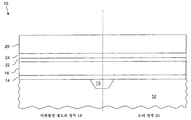
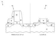
이제 도 2를 참조하면, 제1 게이트 재료층(16)상의 다중 인접 희생층의 증착은 차례로 ARC(anti-reflective coating)층(22), 에칭 정지층(24), 및 연마 정지층(26)의 증착을 포함한다. ARC층(22)이 제1 게이트 재료층(16)상에 형성된다. 바람직한 실시예에서, ARC층(22)은 질화물(예를 들어, TiN), 실리콘 질화물과 같은 금속-실리콘 질화물(예를 들어, TaaSibNc), 금속 함유 질화물, 또는 이것들의 임의 조합이다. 바람직한 실시예에서, ARC층(22)은 기존의 CVD 기술을 사용해 약 155 Å의 두께를 갖도록 증착된다. ARC층(22)은 논리 영역(20)에서 트랜지스터의 게이트를 패터닝하기 위한 반사 방지 코팅으로 사용된다. Referring now to FIG. 2, the deposition of multiple adjacent sacrificial layers on the first
ARC층(22)이 증착된 후, 에칭 정지층(24)이 형성된다. 에칭 정지층(24)은 SiO2와 같은 산화물 등일 수 있다. 일 실시예에서, 에칭 정지층(24)은 80 Å의 두께를 가진 UDOX(ultra-dense oxide layer)이다. 에칭 정지층(24)은 연마 정지층(26)으로부터 ARC층(22)을 분리하는데 사용된다. 에칭 정지층(24)은 에칭 프로세스에서 연마 정지층(26)을 에칭하는 것을 정지시키는데 사용된다. 이와 같이, 에칭 정지층(24)은 제작 동안 수행된 다양한 프로세스로부터 ARC층(22)이 노출되는 것을 방지한다. ARC층(22)은 논리 영역(20)에서 논리 트랜지스터의 게이트 전극을 패터닝하는데 사용될 것이다.After the
일 형태에서, 연마 정지층(26)은 CVD를 사용해 에칭 정지층(24) 두께의 약 5배 두께를 갖도록 증착된다. 연마 정지층(26)은 SiN, SiON 등과 같은 임의 질화물 또는 옥시나이트라이드일 수 있다. 연마 정지층(26)은 CMP 프로세스에서 연마를 정지시키는데 사용된다. 본 발명에서, 연마 정지층은 NVM 영역(18)에서 메모리 트랜지스터용 선택 게이트를 패터닝하기 위한 반사 방지 코팅으로 사용된다.In one form, the polishing
일 형태에서, ARC층(22)은 질소를 포함하고, 에칭 정지층(24)은 산소를 포함하며, 연마 정지층(26)은 질소를 포함한다. In one form, the
도 3은 연마 정지층(26)상에 증착되는 포토레지스트 재료로 이루어진 패터닝된 포토레지스트층(28)을 묘사한다. 패터닝된 포토레지스트층(28)은 기존의 리소그래피 기술, 예를 들어, 스핀-코팅 기술을 사용해 증착된다. 포토레지스트 재료는 리소그래피 적용에 적합한 다양한 포토레지스트 재료를 포함할 수 있다. 포토레지스트 재료는 통상적으로 기반 재료(matrix material) 또는 합성 수지, 감광제(sensitizer) 또는 억제제(inhibitor), 및 용제를 포함한다. 패터닝된 포토레지스트층(28)의 재료는 양성 포토레지스트 재료 또는 음성 포토레지스트 재료일 수 있다. 3 depicts a patterned
도 4에 예시된 바와 같이, 패터닝된 포토레지스트층(28)을 마스크로 사용해 에칭이 수행된다. 에칭은 연마 정지층(26), 에칭 정지층(24), ARC층(22), 및 제1 게이트 재료층(16)을 관통해 에칭하도록 수행된다. 일 실시예에서, 에칭은 건식 에칭 기술을 사용해 수행된다. 패터닝된 포토레지스트층(28)은 에칭 프로세스 이후에 제거된다. 일 실시예에서, 포토레지스트는, RCA 클린, 피라나 클린(piranha clean) 등과 같은, 기존의 습식 클리닝 프로세스를 사용해 제거된다. 다른 실시예에서, 포토레지스트는, 애싱(ashing), 용제 클리닝 등과 같은, 기존의 스트리핑 프로세스(stripping processes)를 사용하는 것에 의해 제거된다. As illustrated in FIG. 4, etching is performed using the patterned
도 5에 표시된 바와 같이, 유전체층(14)의 노출된 영역이 에칭되고, 패터닝된 반도체 장치(10)상에 전하 저장 스택(30)이 증착된다. 전하 저장 스택(30)은 한 층 또는 한 층 이상의 전하 저장 재료이다. 일 실시예에서, 전하 저장 스택(30)은 기존의 증착 기술, 예를 들어, CVD, PECVD(Plasma-enhanced CVD), LPCVD(Low-pressure CVD) 등을 사용해 증착된다. 일 실시예에서, 전하 저장 스택(30)은 산화물 사이에 샌드위치된 나노크리스탈층이다. 다른 실시예에서, 전하 저장 스택(30)은 산화물 사이에 샌드위치된 질화물이다. 또 다른 실시예에서, 전하 저장 스택(30)은 폴리실리콘층인데, ONO(oxide-nitride-oxide)층이 뒤따라 온다. 바람직한 실시예에서, 전하 저장 스택(30)은 산화물 사이에 샌드위치된 나노크리스탈층이다. As shown in FIG. 5, the exposed regions of the
본 발명의 실시예에서는, 패터닝된 반도체 장치(10)상에 전하 저장 스택(30)을 증착하는 대신, NVM 영역(18)의 패터닝된 메모리 트랜지스터를 위한 부동 게이트로서 동작하는 폴리실리콘층이 증착된다. In an embodiment of the present invention, instead of depositing the
도 6을 참조하면, NVM 영역(18) 및 논리 영역(20)상에 제2 게이트 재료층(32)이 증착된다. 제2 게이트 재료층(32)은 전하 저장 스택(30)의 노출된 영역을 채우도록 증착되고 두꺼운 층으로 전하 저장 스택(30)을 덮는다. 제2 게이트 재료층(32)은 금속, 폴리실리콘, 또는 그 둘의 임의 조합일 수 있다. 제2 게이트 재료층(32)은, LPCVD(low pressure chemical vapor deposition), PECVD(plasma-enhanced chemical vapor deposition) 등과 같은, 기존 방법을 사용해 증착된다.Referring to FIG. 6, a second
도 7은 제2 게이트 재료층(32)을 연마한 후의 반도체 장치(10)를 나타낸다. 연마는 제2 게이트 재료층(32) 및, 연마 정지층(26)을 덮는 전하 저장 스택(30)을 제거하도록 수행된다. 제2 게이트 재료층(32)은, CMP(chemical mechanical polishing)와 같은, 종래 기술을 사용해 연마된다. 일 실시예에서, 제2 게이트 재료층(32)은, 기존의 에칭 프로세스를 사용하는 것에 의해, 연마 정지층(26)이 노출될 때까지 에칭된다. 7 shows the
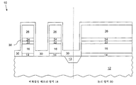
도 8에 따르면, 포토레지스트 재료로 이루어진 포토레지스트 마스크(34)가 증착된다. 그 다음, 노출된 영역으로부터 제2 게이트 재료층(32)이 제거된다. 일 실시예에서, 제2 게이트 재료층(32)은, 비등방성 건식 에칭(non-isotropic dry etch)과 같은, 선택적 건식 에칭 프로세스를 사용하는 것에 의해 제거된다. According to FIG. 8, a
도 9는 도 8의 반도체 장치(10)상에 증착된 포토레지스트 재료로 이루어진 포토레지스트 마스크(36)를 예시한다. 그 다음, 노출된 영역은 건식 에칭 프로세스를 사용해 에칭된다. 본 프로세스에서, 노출된 연마 정지층(26), 에칭 정지층(24), ARC층(22), 및 제1 게이트 재료층(16)이 도 8의 반도체 장치(10)로부터 제거된다. 9 illustrates a
도 10에 예시된 바와 같이, 도 9의 반도체 장치의 연마 정지층(26)은, 비등방성 기술과 같은, 기존의 건식 에칭 프로세스를 사용해 선택적으로 에칭된다. 건식 에칭은, 제2 게이트 재료층(32)은 영향을 받지 않으면서 연마 정지층(26)은 에칭 제거되는 식으로 이루어진다. As illustrated in FIG. 10, the polishing
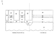
도 11에 예시된 바와 같이, 도 10의 반도체 장치(10)에 대해 습식 에칭 프로세스가 수행된다. 일 형태에서, 습식 에칭 프로세스는, HF(hydrofluoric) 에칭과 같은, 기존의 습식 에칭 프로세스이다. 습식 에칭 프로세스에 사용될 수 있는 다른 산으로는 H3PO4, H2SO4, KOH, H2O2, 및 HCl을 들 수 있지만, 그것으로 제한되는 것은 아니다. 습식 에칭 프로세스는 에칭 정지층(24), 전하 저장 스택(30)의 노출된 영역, 및 노출된 유전체층(14)을 제거한다. 그에 따라, 습식 에칭 프로세스의 완료시에, NVM 영역(18)에서의 선택 게이트 및 제어 게이트 형성이 완료된다. As illustrated in FIG. 11, a wet etching process is performed on the
도 12는, 논리 영역(20)에서 논리 트랜지스터의 게이트를 패터닝하기 위해 증착되는, 포토레지스트 재료로 이루어진 포토레지스트 마스크(38)를 예시한다. 여기에서, 논리 트랜지스터의 게이트는 ARC층(22)을 사용해 패터닝된다. 노출된 ARC층(22) 및 제1 게이트 재료층(16)은 건식 에칭 프로세스를 사용해 도 11의 반도체 장치(10)의 논리 영역(20)으로부터 제거된다. FIG. 12 illustrates a
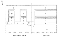
논리 트랜지스터의 게이트가 ARC층(22)을 사용해 패터닝되므로, 본 패터닝에서는 논리 트랜지스터의 게이트를 패터닝하기 위해 게이트 산화물상에 BARC층을 증착할 필요가 없다. 더 나아가, BARC를 증착하는 동안의 비평면성 문제를 감소시키기 위해 트렌치 분리(13)는 크게 만들어진다. NVM 영역(18)과 논리 영역(20) 사이의 트렌치 분리(13)는 최소 포토리소그래피 제한과 연관될 수 있으므로, 집적 회로에서 상당량의 공간이 절약될 수 있다. Since the gate of the logic transistor is patterned using the
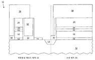
이제 도 13을 참조하면, 포토레지스트 마스크(38) 및 ARC층(22)이 도 12의 반도체 장치(10)로부터 제거된다. 한 세트의 스페이서(40, 42)가 NVM 영역(18)의 제1 게이트 재료층(16) 및 제2 게이트 재료층(32) 주위에 그리고 논리 영역(20)의 제1 게이트 재료층(16) 주위에 각각 형성된다. 스페이서(40, 42) 세트는 기판상에, 산화물, 질화물, 옥시나이트라이드 등과 같은, 절연층을 증착하고 절연층 일부를 에칭하는 것에 의해 형성될 수 있다. 메모리 트랜지스터(52)를 위한 소스(44) 및 드레인(46)이 NVM 영역(18)에 형성된다. 논리 트랜지스터(54)를 위한 소스(48) 및 드레인(50)이 논리 영역(20)에 형성된다. 소스(44, 48) 및 드레인(46, 50)은 기존의 도핑 프로세스에 의해 각각 형성된다. 이와 같이, NVM 영역(18)에서는, 메모리 트랜지스터(52)가 형성되고, 논리 영역(20)에서는, 논리 트랜지스터(54)가 형성된다. 제1 게이트 재료층(16)은 NVM 영역(18)의 메모리 트랜지스터(52)를 위한 선택 게이트로서 동작하고 제2 게이트 재료층(32)은 NVM 영역(18)의 메모리 트랜지스터(52)를 위한 제어 게이트로서 동작한다. 제1 게이트 재료층(16)은 논리 영역(20)의 논리 트랜지스터(54)를 위한 게이트로도 동작한다. Referring now to FIG. 13,
여기에서 사용되는 바와 같이, NVM 영역, 제1 정의 영역, 및 제1 영역이란 용어는 반도체 장치(10)에서의 메모리 영역을 표현하고, 논리 영역, 제2 정의 영역, 및 제2 영역이란 용어는 반도체 장치(10)에서의 논리 영역을 표현한다.As used herein, the terms NVM region, first definition region, and first region refer to a memory region in the
여기에서 사용되는 바와 같이, "제1 게이트 재료층" 및 "제1 게이트 전극 재료"란 용어는 NVM 영역(18)에서의 선택 게이트 뿐만 아니라 논리 영역(20)에서의 게이트 전극을 표현한다. "제2 게이트 재료층" 및 "제2 게이트 전극 재료"란 용어는 NVM 영역(18)에서의 제어 게이트를 표현한다. As used herein, the terms "first gate material layer" and "first gate electrode material" refer to gate electrodes in logic region 20 as well as select gates in NVM region 18. The terms "second gate material layer" and "second gate electrode material" represent control gates in the NVM region 18.
여기에서 사용되는 바와 같이, "제1 장치 유형" 및 "메모리 트랜지스터"란 용어는 메모리 영역에서의 트랜지스터를 표현하고, "제2 장치 유형" 및 "논리 트랜지스터"란 용어는 논리 영역에서 논리 기능을 수행하는데 사용되는 트랜지스터를 표현한다. As used herein, the terms "first device type" and "memory transistor" refer to transistors in a memory region, and the terms "second device type" and "logical transistor" refer to logic functions in a logical region. Represents a transistor used to perform.
여기에서 설명되는 구조는 질화물, 산화물, 및 질화물(ARC층)의 스택을 포함하는 다중 희생층을 이용해 메모리 회로 영역에서의 메모리 트랜지스터의 선택 게이트 및 논리 회로 영역에서의 논리 트랜지스터의 게이트 전극을 패터닝한다. 이와 같이, NVM 및 논리 장치의 통합에 따른 프로세스 복잡도는 크게 감소된다. 논리 영역에서의 게이트 전극을 패터닝하기 위해 BARC층을 사용하는 대신에, 본 발명은 질화물/산화물/질화물 스택으로부터의 ARC층을 이 목적에 사용한다. 이 때문에, 트렌치 분리 영역의 사이즈가 커질 필요가 없어 SoC에서의 최적 공간 이용을 유도한다. 더 나아가, 본 발명은 NVM 메모리의 SoC로의 심리스 통합(seamless integration)을 가능하게 한다. The structure described herein patterns multiple gates of a memory transistor in the memory circuit region and a gate electrode of the logic transistor in the logic circuit region using multiple sacrificial layers comprising a stack of nitride, oxide, and nitride (ARC layer). . As such, the process complexity of integrating NVM and logic devices is greatly reduced. Instead of using a BARC layer to pattern the gate electrode in the logic region, the present invention uses an ARC layer from a nitride / oxide / nitride stack for this purpose. For this reason, the size of the trench isolation region does not need to be large, leading to optimal space utilization in the SoC. Furthermore, the present invention enables seamless integration of NVM memory into SoCs.
일 형태에서는, 제1 정의 영역 및 제1 정의 영역으로부터 전기적으로 분리되는 제2 정의 영역을 가진 기판을 제공하는 것에 의해 NVM 회로와 논리 회로를 통합하는 방법이 제공된다. 제1 정의 영역 및 제2 정의 영역 양자에 기판을 덮는 제1 게이트 재료층이 제공된다. 제1 게이트 재료층을 덮는 다중 인접 희생층이 제공된다. 다중 인접 희생층은, 인접 희생층들 중 적어도 하나가 완전히 제거되지 않은 제1 정의 영역에 트랜지스터 제어 전극을 형성하도록 제공된다. 인접한 희생층 중 적어도 하나는 제2 정의 영역에서 트랜지스터 제어 전극을 패터닝하는데 사용된다. 제1 정의 영역 및 제2 정의 영역 양자에서의 트랜지스터 형성이 완료된다. In one aspect, a method of integrating NVM circuitry and logic circuitry is provided by providing a substrate having a first defining region and a second defining region that is electrically separated from the first defining region. A first gate material layer covering the substrate is provided in both the first defining region and the second defining region. Multiple adjacent sacrificial layers are provided covering the first gate material layer. Multiple adjacent sacrificial layers are provided to form transistor control electrodes in a first defining region in which at least one of the adjacent sacrificial layers has not been completely removed. At least one of the adjacent sacrificial layers is used to pattern the transistor control electrode in the second defining region. Transistor formation in both the first positive region and the second positive region is completed.
다른 형태에서는, 인접한 희생층 중 적어도 하나가 제2 정의 영역에서의 트랜지스터 제어 전극과 밀착하여 인접하다. 또 다른 형태에서, 다중 인접 희생층은 제2 질화물층을 덮는 산화물층을 덮는 제1 질화물층을 더 포함한다. 또 다른 형태에서, 제1 정의 영역은 비휘발성 메모리 셀을 구현하기 위한 비휘발성 메모리 영역을 포함하고, 제2 정의 영역은 논리 기능을 구현하는 트랜지스터를 구현하기 위한 논리 영역을 포함한다. 또 다른 형태에서, 제1 정의 영역은 최소 포토리소그래피 제한에 대응하는 양만큼 제2 정의 영역으로부터 전기적으로 분리된다. 또 다른 형태에서, 다중 인접 희생층 중 적어도 하나는 CMP(chemical mechanical polishing)에서 사용하기 위한 연마 정지층을 포함하고, 다중 인접 희생층 중 적어도 하나는 화학적 에칭에서 사용하기 위한 에칭 정지층을 포함하며, 다중 인접 희생층 중 적어도 하나는 ARC(anti-reflective coating)층을 포함한다. 또 다른 형태에서, 다중 인접 희생층은 제1 정의 영역 및 제2 정의 영역의 프로세싱 완료시에 완전히 제거된다. 일 형태에서, 다중 인접 희생층은 기판을 덮는 ARC층, ARC층을 덮는 산화물층, 및 산화물층을 덮는 질화물층을 포함한다.In another embodiment, at least one of the adjacent sacrificial layers is in close contact with the transistor control electrode in the second defining region. In another form, the multiple adjacent sacrificial layers further comprise a first nitride layer covering an oxide layer covering the second nitride layer. In another form, the first definition region includes a nonvolatile memory region for implementing a nonvolatile memory cell, and the second definition region includes a logic region for implementing a transistor that implements a logic function. In another form, the first defining region is electrically separated from the second defining region by an amount corresponding to the minimum photolithography limit. In another form, at least one of the multiple adjacent sacrificial layers includes a polishing stop layer for use in chemical mechanical polishing (CMP), and at least one of the multiple adjacent sacrificial layers includes an etch stop layer for use in chemical etching. At least one of the multiple adjacent sacrificial layers includes an anti-reflective coating (ARC) layer. In another form, the multiple adjacent sacrificial layers are completely removed upon completion of processing of the first definition region and the second definition region. In one form, the multiple adjacent sacrificial layers include an ARC layer covering the substrate, an oxide layer covering the ARC layer, and a nitride layer covering the oxide layer.
또 다른 형태에서는, 기판상에 형성되어 분리 영역에 의해 분리되는 제1 영역 및 제2 영역을 포함하는 집적 회로 형성 방법이 제공된다. 제1 영역 및 제2 영역 양자에 기판을 덮는 제1 게이트 전극 재료층이 형성된다. 제1 영역 및 제2 영역에 어떤 장치를 형성하기에 앞서, 제1 영역 및 제2 영역 양자에 제1 게이트 전극 재료층을 덮는 복수개 희생층이 형성된다. 복수개 희생층은 제1 영역에서 제1 장치 유형을 형성하는데 사용된다. 복수개 희생층 중 적어도 하나는 제2 영역에서 제2 장치 유형을 형성하는데 사용된다. In another aspect, an integrated circuit forming method is provided that includes a first region and a second region formed on a substrate and separated by a separation region. A first gate electrode material layer covering the substrate is formed in both the first region and the second region. Prior to forming any device in the first region and the second region, a plurality of sacrificial layers covering the first gate electrode material layer are formed in both the first region and the second region. A plurality of sacrificial layers is used to form the first device type in the first region. At least one of the plurality of sacrificial layers is used to form the second device type in the second region.
또 다른 형태에서는, 제2 영역에 제2 장치 유형에 대응하는 게이트 전극을 형성하기에 앞서, 제1 영역으로부터 복수개 희생층이 제거된다. 또 다른 형태에서는, 복수개 희생층 중 제1 게이트 전극 재료층에 밀착하여 인접한 적어도 하나가 제2 장치 유형을 형성하는데 사용된다. 또 다른 형태에서는, 제2 장치 유형을 형성하는데 사용되는 복수개 희생층 중 적어도 하나가 ARC층이다. 또 다른 형태에서는, 제2 영역에 제2 장치 유형에 대응하는 게이트 전극을 패터닝하는데 사용되는 ARC층이 형성된다. 또 다른 형태에서, 복수개 희생층은 제2 영역에 형성된 제2 장치 유형에 대응하는 게이트 전극을 패터닝하는데 사용되는 ARC층, 제1 영역 및 제2 영역 양자에 형성된 폴리실리콘층의 연마를 정지시키는데 사용되는 연마 정지층, 그리고 제1 영역 및 제2 영역 양자에서 연마 정지층을 에칭하는 것을 정지시키는데 사용되는 에칭 정지층을 포함한다. 또 다른 형태에서, 제1 영역은 메모리 영역이고 제2 영역은 논리 영역이다. 또 다른 형태에서, 제1 장치 유형은 제어 게이트 및 선택 게이트를 포함하고, 제2 장치 유형은 하나의 게이트만을 포함한다. In another form, the plurality of sacrificial layers are removed from the first region prior to forming the gate electrode corresponding to the second device type in the second region. In another form, at least one adjacent to and in close contact with the first gate electrode material layer of the plurality of sacrificial layers is used to form the second device type. In another form, at least one of the plurality of sacrificial layers used to form the second device type is an ARC layer. In another form, an ARC layer is formed in the second region that is used to pattern the gate electrode corresponding to the second device type. In another form, the plurality of sacrificial layers is used to stop polishing of the ARC layer, the first and second polysilicon layers formed in both the first and second regions, used to pattern the gate electrode corresponding to the second device type formed in the second region. A polishing stop layer, and an etch stop layer used to stop etching the polishing stop layer in both the first region and the second region. In another form, the first region is a memory region and the second region is a logic region. In another form, the first device type includes a control gate and a select gate, and the second device type includes only one gate.
또 다른 형태에서는, 기판상에 형성되어 분리 영역에 의해 분리되는 메모리 영역 및 논리 영역을 포함하는 집적 회로 형성 방법이 제공된다. 메모리 영역 및 논리 영역 양자에 기판을 덮는 제1 게이트 전극 재료층이 형성된다. 메모리 영역 및 논리 영역에 어떤 장치를 형성하기에 앞서, 메모리 영역 및 논리 영역 양자에 제1 게이트 전극 재료층을 덮는 복수개 희생층이 형성된다. 복수개 희생층은 메모리 영역에 비휘발성 메모리 장치를 형성하는데 사용된다. 복수개 희생층 중 적어도 하나는 논리 영역에 논리 장치를 형성하는데 사용되는데, 이 경우, 논리 장치를 형성하는데 사용되는 복수개 희생층 중 적어도 하나는 논리 영역에 대응하는 게이트 전극을 패터닝하는데 사용되는 ARC층이다. 또 다른 형태에서는, 논리 영역에 논리 장치에 대응하는 게이트 전극을 형성하기에 앞서, 복수개 희생층이 메모리 영역으로부터 제거된다. 또 다른 형태에서, 논리 장치를 형성하는데 사용되는 복수개 희생층 중 적어도 하나는 제1 게이트 전극 재료층에 밀착하여 인접하다. 또 다른 형태에서, 복수개 희생층은 메모리 영역 및 논리 영역 양자에 형성된 폴리실리콘층의 연마를 정지시키는데 사용되는 연마 정지층을 그리고 메모리 영역 및 논리 영역 양자에서 연마 정지층을 에칭하는 것을 정지시키는데 사용되는 에칭 정지층을 포함한다. 또 다른 형태에서, ARC층은 질소를 포함하고, 연마 정지층도 질소를 포함하며, 에칭 정지층은 산소를 포함한다. In yet another aspect, an integrated circuit forming method is provided that includes a memory region and a logic region formed on a substrate and separated by isolation regions. A first gate electrode material layer covering the substrate is formed in both the memory region and the logic region. Prior to forming any device in the memory region and the logic region, a plurality of sacrificial layers covering the first gate electrode material layer are formed in both the memory region and the logic region. The plurality of sacrificial layers are used to form a nonvolatile memory device in the memory area. At least one of the plurality of sacrificial layers is used to form a logic device in the logic region, in which case at least one of the plurality of sacrificial layers used to form the logic device is an ARC layer used to pattern the gate electrode corresponding to the logic region. . In another embodiment, the plurality of sacrificial layers is removed from the memory region prior to forming the gate electrode corresponding to the logic device in the logic region. In another form, at least one of the plurality of sacrificial layers used to form the logic device is adjacent to and in close contact with the first gate electrode material layer. In another form, the plurality of sacrificial layers is used to stop polishing the polishing stop layer used to stop polishing the polysilicon layer formed in both the memory region and the logic region and to etch the polishing stop layer in both the memory region and the logic region. And an etch stop layer. In another form, the ARC layer comprises nitrogen, the polishing stop layer also includes nitrogen, and the etch stop layer comprises oxygen.
일반적인 설명 또는 일례로서 앞서 설명된 모든 활동이 요구되는 것은 아니라는 것, 특정 활동의 일부는 불필요할 수도 있다는 것, 그리고 설명된 활동에 추가하여 하나 이상의 추가 활동이 수행될 수도 있다는 것에 유의해야 한다. 더 나아가, 활동이 열거되는 순서가 반드시 활동이 수행되는 순서일 필요는 없다.It should be noted that not all of the activities described above as a general description or example are required, that some of the specific activities may be unnecessary, and that one or more additional activities may be performed in addition to the described activities. Furthermore, the order in which the activities are listed does not necessarily have to be the order in which the activities are performed.
하나 이상의 어떤 혜택, 하나 이상의 다른 장점, 하나 이상의 문제에 대한 하나 이상의 해결책, 또는 이것들의 임의 조합이 하나 이상의 특정 실시예와 관련하여 상술되었다. 그러나, 어떤 혜택, 장점, 또는 해결책을 발생시킬 수 있거나 좀 더 명확하게 할 수 있는 혜택, 장점, 문제에 대한 해결책, 또는 어떤 요소가 어떤 청구항 또는 모든 청구항의 중요하거나, 필요하거나, 필수적인 특징 또는 요소로 간주되어서는 안된다. One or more certain benefits, one or more other advantages, one or more solutions to one or more problems, or any combination thereof, have been described above with reference to one or more specific embodiments. However, any benefit, advantage, solution to a problem, or element that may generate or be made clearer of any benefit, advantage, or solution is an important, necessary, or essential feature or element of any claim or all claims. It should not be considered as.
앞서 설명된 주제는 한정적인 것이 아니라 예시적인 것으로 간주되어야 하고, 첨부된 청구항은 본 발명의 범위내에 해당되는 그러한 모든 변경, 향상, 및 다른 실시예를 포괄하기 위한 것이다. 따라서, 법에 의해 허용되는 최대 한도까지, 본 발명의 범위는 다음 청구항 및 그것의 균등물의 허용 가능한 최대 해석에 의해 판정되어야 하고, 앞서 말한 상세한 설명에 의해 한정되거나 제한되지 않을 것이다.The subject matter described above should be regarded as illustrative rather than restrictive, and the appended claims are intended to cover all such alterations, enhancements, and other embodiments that fall within the scope of the invention. Thus, to the maximum extent permitted by law, the scope of the present invention should be determined by the maximum allowable interpretation of the following claims and their equivalents, and shall not be limited or limited by the foregoing detailed description.
10 : 반도체 장치
12 : 기판
13 : 트렌치 분리
14 : 유전체층
16 : 제1 게이트 재료층10: semiconductor device
12: substrate
13: trench isolation
14: dielectric layer
16: first gate material layer
Claims (20)
상기 제1 정의 영역 및 상기 제2 정의 영역 양자에 상기 기판을 덮는(overlying) 제1 게이트 재료층을 제공하는 단계;
상기 제1 게이트 재료층을 덮는 다중 인접 희생층(multiple adjoining sacrificial layers)을 제공하는 단계;
상기 다중 인접 희생층을 사용해 상기 제1 정의 영역에 트랜지스터 제어 전극들을 형성하는 단계 - 상기 인접 희생층들 중 적어도 하나는 완전히 제거되지 않음 -;
상기 인접 희생층들 중 적어도 하나를 사용해 상기 제2 정의 영역에 트랜지스터 제어 전극을 패터닝하는 단계; 및
상기 제1 정의 영역 및 상기 제2 정의 영역 양자에서 트랜지스터 형성을 완료하는 단계
를 포함하는 방법. Providing a substrate having a first defining region and a second defining region electrically separated from the first defining region;
Providing a first gate material layer overlying said substrate in both said first defined region and said second defined region;
Providing multiple adjoining sacrificial layers covering the first gate material layer;
Forming transistor control electrodes in the first defining region using the multiple adjacent sacrificial layers, at least one of the adjacent sacrificial layers not completely removed;
Patterning a transistor control electrode in said second defining region using at least one of said adjacent sacrificial layers; And
Completing transistor formation in both the first definition region and the second definition region
How to include.
상기 인접 희생층들 중 적어도 하나는 상기 제2 정의 영역에서의 상기 트랜지스터 제어 전극에 바로 인접하는(immediately adjacent) 방법. The method of claim 1,
At least one of the adjacent sacrificial layers is immediately adjacent to the transistor control electrode in the second defining region.
상기 다중 인접 희생층은 제2 질화물층을 덮는 산화물층을 덮는 제1 질화물층을 더 포함하는 방법. The method of claim 1,
And wherein the multiple adjacent sacrificial layer further comprises a first nitride layer covering an oxide layer covering a second nitride layer.
상기 제1 정의 영역은 비휘발성 메모리 셀들을 구현하기 위한 비휘발성 메모리 영역을 포함하고, 상기 제2 정의 영역은 논리 기능들을 구현하는 트랜지스터들을 구현하기 위한 논리 영역을 포함하는 방법. The method of claim 1,
Wherein the first definition region includes a nonvolatile memory region for implementing nonvolatile memory cells, and the second definition region includes a logic region for implementing transistors that implement logic functions.
상기 제1 정의 영역은 최소 포토리소그래피 제한에 대응하는 양만큼 상기 제2 정의 영역으로부터 전기적으로 분리되는 방법. The method of claim 1,
The first defining region is electrically separated from the second defining region by an amount corresponding to a minimum photolithography limit.
상기 다중 인접 희생층 중 적어도 하나는 CMP(chemical mechanical polishing)에서 사용하기 위한 연마 정지층을 포함하고, 상기 다중 인접 희생층 중 적어도 하나는 화학적 에칭에서 사용하기 위한 에칭 정지층을 포함하며, 상기 다중 인접 희생층 중 적어도 하나는 ARC(anti-reflective coating)층을 포함하는 방법. The method of claim 1,
At least one of the multiple adjacent sacrificial layers includes a polishing stop layer for use in chemical mechanical polishing (CMP), at least one of the multiple adjacent sacrificial layers includes an etch stop layer for use in chemical etching, and the multiple At least one of the adjacent sacrificial layers comprises an anti-reflective coating (ARC) layer.
상기 다중 인접 희생층은 상기 제1 정의 영역 및 상기 제2 정의 영역에 대한 프로세싱의 완료시에 완전히 제거되고,
상기 기판을 덮는 ARC층;
상기 ARC층을 덮는 산화물층; 및
상기 산화물층을 덮는 질화물층을 더 포함하는 방법. The method of claim 1,
The multiple adjacent sacrificial layers are completely removed upon completion of processing for the first and second defining regions,
An ARC layer covering the substrate;
An oxide layer covering the ARC layer; And
And a nitride layer covering the oxide layer.
상기 제1 영역 및 상기 제2 영역 양자에 상기 기판을 덮는 제1 게이트 전극 재료층을 형성하는 단계;
상기 제1 영역 및 상기 제2 영역에 임의의 장치들을 형성하기에 앞서, 상기 제1 영역 및 상기 제2 영역 양자에 상기 제1 게이트 전극 재료층을 덮는 복수개 희생층을 형성하는 단계;
상기 복수개 희생층을 사용해 상기 제1 영역에 제1 장치 유형을 형성하는 단계; 및
상기 복수개 희생층 중 적어도 하나를 사용해 상기 제2 영역에 제2 장치 유형을 형성하는 단계
를 포함하는 방법. A method of forming an integrated circuit comprising a first region and a second region formed on a substrate and separated by a separation region, the method comprising:
Forming a first gate electrode material layer covering the substrate in both the first region and the second region;
Prior to forming any devices in the first region and the second region, forming a plurality of sacrificial layers covering the first gate electrode material layer in both the first region and the second region;
Forming a first device type in the first region using the plurality of sacrificial layers; And
Forming a second device type in the second region using at least one of the plurality of sacrificial layers
How to include.
상기 제2 영역에서의 상기 제2 장치 유형에 대응하는 게이트 전극들을 형성하기에 앞서, 상기 복수개 희생층을 상기 제1 영역으로부터 제거하는 단계를 더 포함하는 방법. The method of claim 8,
Prior to forming gate electrodes corresponding to the second device type in the second region, removing the plurality of sacrificial layers from the first region.
상기 제2 장치 유형을 형성하는데 사용되는 상기 복수개 희생층 중 적어도 하나는 상기 제1 게이트 전극 재료층에 바로 인접하는 방법. The method of claim 8,
At least one of the plurality of sacrificial layers used to form the second device type is directly adjacent to the first gate electrode material layer.
상기 제2 장치 유형을 형성하는데 사용되는 상기 복수개 희생층 중 적어도 하나는 ARC층인 방법. The method of claim 8,
At least one of the plurality of sacrificial layers used to form the second device type is an ARC layer.
상기 ARC층은 상기 제2 영역에 형성된 상기 제2 장치 유형에 대응하는 게이트 전극을 패터닝하는데 사용되는 방법. The method of claim 11,
Wherein the ARC layer is used to pattern a gate electrode corresponding to the second device type formed in the second region.
상기 복수개 희생층은 상기 제2 영역에 형성된 상기 제2 장치 유형에 대응하는 게이트 전극을 패터닝하는데 사용되는 ARC층, 상기 제1 영역 및 상기 제2 영역 양자에 형성된 폴리실리콘층의 연마를 정지시키는데 사용되는 연마 정지층, 및 상기 제1 영역 및 상기 제2 영역 양자에서 상기 연마 정지층을 에칭하는 것을 정지시키는데 사용되는 에칭 정지층을 포함하는 방법. The method of claim 8,
The plurality of sacrificial layers are used to stop polishing of the ARC layer used to pattern the gate electrode corresponding to the second device type formed in the second region, the polysilicon layer formed in both the first region and the second region. A polishing stop layer, and an etch stop layer used to stop etching the polishing stop layer in both the first region and the second region.
상기 제1 영역은 메모리 영역이고, 상기 제2 영역은 논리 영역인 방법. The method of claim 8,
Wherein the first area is a memory area and the second area is a logical area.
상기 제1 장치 유형은 제어 게이트 및 선택 게이트를 포함하고, 상기 제2 장치 유형은 하나의 게이트만을 포함하는 방법. The method of claim 14,
Wherein the first device type includes a control gate and a select gate, and the second device type includes only one gate.
상기 메모리 영역 및 상기 논리 영역 양자에 상기 기판을 덮는 제1 게이트 전극 재료층을 형성하는 단계;
상기 메모리 영역 및 상기 논리 영역에 임의의 장치들을 형성하기에 앞서, 상기 메모리 영역 및 상기 논리 영역 양자에 상기 제1 게이트 전극 재료층을 덮는 복수개 희생층을 형성하는 단계;
상기 복수개 희생층을 사용해 상기 메모리 영역에 비휘발성 메모리 장치를 형성하는 단계; 및
상기 복수개 희생층 중 적어도 하나를 사용해 상기 논리 영역에 논리 장치를 형성하는 단계 - 상기 논리 장치를 형성하는데 사용되는 상기 복수개 희생층 중 적어도 하나는 상기 논리 영역에 대응하는 게이트 전극을 패터닝하는데 사용되는 ARC층임 -;
를 포함하는 방법. A method of forming an integrated circuit comprising a memory region and a logic region formed on a substrate and separated by isolation regions, the method comprising:
Forming a first gate electrode material layer covering the substrate in both the memory region and the logic region;
Prior to forming any devices in the memory region and the logic region, forming a plurality of sacrificial layers covering the first gate electrode material layer in both the memory region and the logic region;
Forming a nonvolatile memory device in the memory area using the plurality of sacrificial layers; And
Forming a logic device in the logic region using at least one of the plurality of sacrificial layers, wherein at least one of the plurality of sacrificial layers used to form the logic device is used to pattern a gate electrode corresponding to the logic region Layer;
How to include.
상기 논리 영역에 상기 논리 장치에 대응하는 상기 게이트 전극을 형성하기에 앞서, 상기 복수개 희생층을 상기 메모리 영역으로부터 제거하는 단계를 더 포함하는 방법. The method of claim 16,
Prior to forming the gate electrode corresponding to the logic device in the logic region, removing the plurality of sacrificial layers from the memory region.
상기 논리 장치를 형성하는데 사용되는 상기 복수개 희생층 중 적어도 하나는 상기 제1 게이트 전극 재료층에 바로 인접하는 방법. The method of claim 16,
At least one of the plurality of sacrificial layers used to form the logic device is immediately adjacent to the first gate electrode material layer.
상기 복수개 희생층은 상기 메모리 영역 및 상기 논리 영역 양자에 형성된 폴리실리콘층의 연마를 정지시키는데 사용되는 연마 정지층, 및 상기 메모리 영역 및 상기 논리 영역 양자에서 상기 연마 정지층을 에칭하는 것을 정지시키는데 사용되는 에칭 정지층을 포함하는 방법. The method of claim 16,
The plurality of sacrificial layers are used to stop etching the polishing stop layer used to stop polishing the polysilicon layer formed in both the memory region and the logic region, and the polishing stop layer in both the memory region and the logic region. And an etch stop layer.
상기 ARC층은 질소를 포함하고, 상기 연마 정지층은 질소를 포함하며, 상기 에칭 정지층은 산소를 포함하는 방법.The method of claim 19,
The ARC layer comprises nitrogen, the polishing stop layer comprises nitrogen, and the etch stop layer comprises oxygen.
Applications Claiming Priority (2)
| Application Number | Priority Date | Filing Date | Title |
|---|---|---|---|
| US11/926,348 | 2007-10-29 | ||
| US11/926,348 US7745344B2 (en) | 2007-10-29 | 2007-10-29 | Method for integrating NVM circuitry with logic circuitry |
Publications (1)
| Publication Number | Publication Date |
|---|---|
| KR20100084164A true KR20100084164A (en) | 2010-07-23 |
Family
ID=40583356
Family Applications (1)
| Application Number | Title | Priority Date | Filing Date |
|---|---|---|---|
| KR1020107009304A KR20100084164A (en) | 2007-10-29 | 2008-09-18 | Method for integrating nvm circuitry with logic circuitry |
Country Status (8)
| Country | Link |
|---|---|
| US (1) | US7745344B2 (en) |
| EP (1) | EP2206151B1 (en) |
| JP (1) | JP2011502353A (en) |
| KR (1) | KR20100084164A (en) |
| CN (1) | CN101842899B (en) |
| AT (1) | ATE554501T1 (en) |
| TW (1) | TWI437667B (en) |
| WO (1) | WO2009058486A1 (en) |
Cited By (1)
| Publication number | Priority date | Publication date | Assignee | Title |
|---|---|---|---|---|
| KR20120021271A (en) * | 2010-08-31 | 2012-03-08 | 프리스케일 세미컨덕터, 인크. | Patterning a gate stack of a non-volatile memory(nvm) with simultaneous etch in non-nvm area |
Families Citing this family (37)
| Publication number | Priority date | Publication date | Assignee | Title |
|---|---|---|---|---|
| JP2010067645A (en) * | 2008-09-08 | 2010-03-25 | Renesas Technology Corp | Semiconductor device and method of manufacturing the same |
| FR2959349B1 (en) * | 2010-04-22 | 2012-09-21 | Commissariat Energie Atomique | MANUFACTURING A MEMORY WITH TWO SELF-ALIGNED INDEPENDENT GRIDS |
| US8399310B2 (en) | 2010-10-29 | 2013-03-19 | Freescale Semiconductor, Inc. | Non-volatile memory and logic circuit process integration |
| US8906764B2 (en) | 2012-01-04 | 2014-12-09 | Freescale Semiconductor, Inc. | Non-volatile memory (NVM) and logic integration |
| US8669158B2 (en) | 2012-01-04 | 2014-03-11 | Mark D. Hall | Non-volatile memory (NVM) and logic integration |
| US8658497B2 (en) | 2012-01-04 | 2014-02-25 | Freescale Semiconductor, Inc. | Non-volatile memory (NVM) and logic integration |
| US8951863B2 (en) | 2012-04-06 | 2015-02-10 | Freescale Semiconductor, Inc. | Non-volatile memory (NVM) and logic integration |
| US8722493B2 (en) | 2012-04-09 | 2014-05-13 | Freescale Semiconductor, Inc. | Logic transistor and non-volatile memory cell integration |
| US9087913B2 (en) | 2012-04-09 | 2015-07-21 | Freescale Semiconductor, Inc. | Integration technique using thermal oxide select gate dielectric for select gate and apartial replacement gate for logic |
| US8728886B2 (en) | 2012-06-08 | 2014-05-20 | Freescale Semiconductor, Inc. | Integrating formation of a replacement gate transistor and a non-volatile memory cell using a high-k dielectric |
| TWI485811B (en) * | 2012-07-18 | 2015-05-21 | Maxchip Electronics Corp | Method of forming semiconductor structure |
| US9111865B2 (en) * | 2012-10-26 | 2015-08-18 | Freescale Semiconductor, Inc. | Method of making a logic transistor and a non-volatile memory (NVM) cell |
| JP6026914B2 (en) * | 2013-02-12 | 2016-11-16 | ルネサスエレクトロニクス株式会社 | Manufacturing method of semiconductor device |
| US8741719B1 (en) | 2013-03-08 | 2014-06-03 | Freescale Semiconductor, Inc. | Integrating formation of a logic transistor and a non-volatile memory cell using a partial replacement gate technique |
| US8716089B1 (en) | 2013-03-08 | 2014-05-06 | Freescale Semiconductor, Inc. | Integrating formation of a replacement gate transistor and a non-volatile memory cell having thin film storage |
| US9006093B2 (en) | 2013-06-27 | 2015-04-14 | Freescale Semiconductor, Inc. | Non-volatile memory (NVM) and high voltage transistor integration |
| CN104347514B (en) * | 2013-07-30 | 2017-08-01 | 中芯国际集成电路制造(上海)有限公司 | A kind of preparation method of embedded flash memory |
| US8877585B1 (en) | 2013-08-16 | 2014-11-04 | Freescale Semiconductor, Inc. | Non-volatile memory (NVM) cell, high voltage transistor, and high-K and metal gate transistor integration |
| US9129996B2 (en) | 2013-07-31 | 2015-09-08 | Freescale Semiconductor, Inc. | Non-volatile memory (NVM) cell and high-K and metal gate transistor integration |
| US8871598B1 (en) | 2013-07-31 | 2014-10-28 | Freescale Semiconductor, Inc. | Non-volatile memory (NVM) and high-k and metal gate integration using gate-first methodology |
| US9082837B2 (en) | 2013-08-08 | 2015-07-14 | Freescale Semiconductor, Inc. | Nonvolatile memory bitcell with inlaid high k metal select gate |
| US9252246B2 (en) | 2013-08-21 | 2016-02-02 | Freescale Semiconductor, Inc. | Integrated split gate non-volatile memory cell and logic device |
| US9082650B2 (en) | 2013-08-21 | 2015-07-14 | Freescale Semiconductor, Inc. | Integrated split gate non-volatile memory cell and logic structure |
| US9275864B2 (en) | 2013-08-22 | 2016-03-01 | Freescale Semiconductor,Inc. | Method to form a polysilicon nanocrystal thin film storage bitcell within a high k metal gate platform technology using a gate last process to form transistor gates |
| US8932925B1 (en) * | 2013-08-22 | 2015-01-13 | Freescale Semiconductor, Inc. | Split-gate non-volatile memory (NVM) cell and device structure integration |
| US9136129B2 (en) | 2013-09-30 | 2015-09-15 | Freescale Semiconductor, Inc. | Non-volatile memory (NVM) and high-k and metal gate integration using gate-last methodology |
| US9129855B2 (en) | 2013-09-30 | 2015-09-08 | Freescale Semiconductor, Inc. | Non-volatile memory (NVM) and high-k and metal gate integration using gate-first methodology |
| US8901632B1 (en) | 2013-09-30 | 2014-12-02 | Freescale Semiconductor, Inc. | Non-volatile memory (NVM) and high-K and metal gate integration using gate-last methodology |
| US9231077B2 (en) | 2014-03-03 | 2016-01-05 | Freescale Semiconductor, Inc. | Method of making a logic transistor and non-volatile memory (NVM) cell |
| US9252152B2 (en) | 2014-03-28 | 2016-02-02 | Freescale Semiconductor, Inc. | Method for forming a split-gate device |
| US9472418B2 (en) | 2014-03-28 | 2016-10-18 | Freescale Semiconductor, Inc. | Method for forming a split-gate device |
| US9112056B1 (en) | 2014-03-28 | 2015-08-18 | Freescale Semiconductor, Inc. | Method for forming a split-gate device |
| US9257445B2 (en) * | 2014-05-30 | 2016-02-09 | Freescale Semiconductor, Inc. | Method of making a split gate non-volatile memory (NVM) cell and a logic transistor |
| US9379222B2 (en) | 2014-05-30 | 2016-06-28 | Freescale Semiconductor, Inc. | Method of making a split gate non-volatile memory (NVM) cell |
| US9343314B2 (en) | 2014-05-30 | 2016-05-17 | Freescale Semiconductor, Inc. | Split gate nanocrystal memory integration |
| CN105336698B (en) * | 2014-07-10 | 2018-11-16 | 中芯国际集成电路制造(上海)有限公司 | The manufacturing method of semiconductor devices |
| US10134748B2 (en) * | 2016-11-29 | 2018-11-20 | Taiwan Semiconductor Manufacturing Co., Ltd. | Cell boundary structure for embedded memory |
Family Cites Families (24)
| Publication number | Priority date | Publication date | Assignee | Title |
|---|---|---|---|---|
| JP2664685B2 (en) * | 1987-07-31 | 1997-10-15 | 株式会社東芝 | Method for manufacturing semiconductor device |
| JP3107199B2 (en) | 1996-08-29 | 2000-11-06 | 日本電気株式会社 | Manufacturing method of nonvolatile semiconductor memory device |
| US6236101B1 (en) * | 1997-11-05 | 2001-05-22 | Texas Instruments Incorporated | Metallization outside protective overcoat for improved capacitors and inductors |
| US6271143B1 (en) * | 1999-05-06 | 2001-08-07 | Motorola, Inc. | Method for preventing trench fill erosion |
| US6323047B1 (en) | 1999-08-03 | 2001-11-27 | Advanced Micro Devices, Inc. | Method for monitoring second gate over-etch in a semiconductor device |
| KR100555485B1 (en) | 1999-09-13 | 2006-03-03 | 삼성전자주식회사 | Method for fabricating flash memory device |
| JP4096507B2 (en) * | 2000-09-29 | 2008-06-04 | 富士通株式会社 | Manufacturing method of semiconductor device |
| US6509235B2 (en) | 2001-01-19 | 2003-01-21 | United Microelectronics Corp. | Method for making an embedded memory MOS |
| US6559059B2 (en) | 2001-01-19 | 2003-05-06 | United Microelectronics Corp. | Method for fabricating a MOS transistor of an embedded memory |
| US6531350B2 (en) | 2001-02-22 | 2003-03-11 | Halo, Inc. | Twin MONOS cell fabrication method and array organization |
| US6808974B2 (en) * | 2001-05-15 | 2004-10-26 | International Business Machines Corporation | CMOS structure with maximized polysilicon gate activation and a method for selectively maximizing doping activation in gate, extension, and source/drain regions |
| US6818504B2 (en) * | 2001-08-10 | 2004-11-16 | Hynix Semiconductor America, Inc. | Processes and structures for self-aligned contact non-volatile memory with peripheral transistors easily modifiable for various technologies and applications |
| US6753242B2 (en) | 2002-03-19 | 2004-06-22 | Motorola, Inc. | Integrated circuit device and method therefor |
| US6875622B1 (en) * | 2002-11-01 | 2005-04-05 | Advanced Micro Devices, Inc. | Method and apparatus for determining electromagnetic properties of a process layer using scatterometry measurements |
| KR100500448B1 (en) * | 2003-02-06 | 2005-07-14 | 삼성전자주식회사 | Method of fabricating a semiconductor integrated circuit using a selective disposable spacer technique and semiconductor integrated circuit fabricated thereby |
| JP4477886B2 (en) * | 2003-04-28 | 2010-06-09 | 株式会社ルネサステクノロジ | Manufacturing method of semiconductor device |
| CN100464429C (en) * | 2003-10-28 | 2009-02-25 | 株式会社半导体能源研究所 | Liquid crystal display device, its manufacturing method, and liquid crystal television receiver |
| US6964902B2 (en) | 2004-02-26 | 2005-11-15 | Freescale Semiconductor, Inc. | Method for removing nanoclusters from selected regions |
| US7361543B2 (en) * | 2004-11-12 | 2008-04-22 | Freescale Semiconductor, Inc. | Method of forming a nanocluster charge storage device |
| US7151302B1 (en) | 2005-06-24 | 2006-12-19 | Freescale Semiconductor, Inc. | Method and apparatus for maintaining topographical uniformity of a semiconductor memory array |
| US7361551B2 (en) * | 2006-02-16 | 2008-04-22 | Freescale Semiconductor, Inc. | Method for making an integrated circuit having an embedded non-volatile memory |
| US7700439B2 (en) * | 2006-03-15 | 2010-04-20 | Freescale Semiconductor, Inc. | Silicided nonvolatile memory and method of making same |
| JP2007281348A (en) * | 2006-04-11 | 2007-10-25 | Renesas Technology Corp | Semiconductor device, and manufacturing method thereof |
| JP2009049338A (en) * | 2007-08-23 | 2009-03-05 | Toshiba Corp | Semiconductor device and method of manufacturing the same |
-
2007
- 2007-10-29 US US11/926,348 patent/US7745344B2/en active Active
-
2008
- 2008-09-18 JP JP2010531101A patent/JP2011502353A/en active Pending
- 2008-09-18 AT AT08844581T patent/ATE554501T1/en active
- 2008-09-18 CN CN2008801140238A patent/CN101842899B/en active Active
- 2008-09-18 WO PCT/US2008/076750 patent/WO2009058486A1/en active Application Filing
- 2008-09-18 KR KR1020107009304A patent/KR20100084164A/en not_active Application Discontinuation
- 2008-09-18 EP EP08844581A patent/EP2206151B1/en active Active
- 2008-10-01 TW TW097137798A patent/TWI437667B/en active
Cited By (1)
| Publication number | Priority date | Publication date | Assignee | Title |
|---|---|---|---|---|
| KR20120021271A (en) * | 2010-08-31 | 2012-03-08 | 프리스케일 세미컨덕터, 인크. | Patterning a gate stack of a non-volatile memory(nvm) with simultaneous etch in non-nvm area |
Also Published As
| Publication number | Publication date |
|---|---|
| EP2206151B1 (en) | 2012-04-18 |
| EP2206151A1 (en) | 2010-07-14 |
| TWI437667B (en) | 2014-05-11 |
| CN101842899A (en) | 2010-09-22 |
| ATE554501T1 (en) | 2012-05-15 |
| WO2009058486A1 (en) | 2009-05-07 |
| US7745344B2 (en) | 2010-06-29 |
| TW200939404A (en) | 2009-09-16 |
| EP2206151A4 (en) | 2010-11-24 |
| US20090111226A1 (en) | 2009-04-30 |
| JP2011502353A (en) | 2011-01-20 |
| CN101842899B (en) | 2012-08-29 |
Similar Documents
| Publication | Publication Date | Title |
|---|---|---|
| US7745344B2 (en) | Method for integrating NVM circuitry with logic circuitry | |
| US7902074B2 (en) | Simplified pitch doubling process flow | |
| US7427552B2 (en) | Method for fabricating isolation structures for flash memory semiconductor devices | |
| US7312158B2 (en) | Method of forming pattern | |
| US7202174B1 (en) | Method of forming micro pattern in semiconductor device | |
| JP5730772B2 (en) | Method for forming split gate memory cell | |
| CN108091562B (en) | ONO etching method of SONOS memory | |
| US7479429B2 (en) | Split game memory cell method | |
| US7169681B2 (en) | Method of forming dual gate dielectric layer | |
| US6197637B1 (en) | Method for fabricating a non-volatile memory cell | |
| KR100673228B1 (en) | Method of manufacturing a nand flash memory device | |
| KR101725978B1 (en) | Method for forming the semiconductor device | |
| CN110620115B (en) | Method for manufacturing 1.5T SONOS flash memory | |
| US6960506B2 (en) | Method of fabricating a memory device having a self-aligned contact | |
| KR100624962B1 (en) | Method of manufacturing a flash memory device | |
| KR100672174B1 (en) | Method of fabricating alignment key in semiconductor device | |
| KR100664789B1 (en) | Method for fabricating float gate in a flash memory | |
| KR100803494B1 (en) | Method for fabricating flash memory device | |
| KR20070051967A (en) | Method of manufacturing a non-volatile memory device | |
| KR20080030289A (en) | Method of manufacturing a flash memory device | |
| KR20050070954A (en) | Method for fabricating flash gate and high voltage gate | |
| KR20060136126A (en) | Method of manufacturing a NAND type flash memory device |
Legal Events
| Date | Code | Title | Description |
|---|---|---|---|
| WITN | Application deemed withdrawn, e.g. because no request for examination was filed or no examination fee was paid |