KR20100057784A - Coarse/fine program verification in non-volatile memory using different reference levels for improved sensing - Google Patents
Coarse/fine program verification in non-volatile memory using different reference levels for improved sensing Download PDFInfo
- Publication number
- KR20100057784A KR20100057784A KR1020107002519A KR20107002519A KR20100057784A KR 20100057784 A KR20100057784 A KR 20100057784A KR 1020107002519 A KR1020107002519 A KR 1020107002519A KR 20107002519 A KR20107002519 A KR 20107002519A KR 20100057784 A KR20100057784 A KR 20100057784A
- Authority
- KR
- South Korea
- Prior art keywords
- programming
- storage elements
- verify level
- voltage
- level
- Prior art date
Links
Images


Classifications
-
- G—PHYSICS
- G11—INFORMATION STORAGE
- G11C—STATIC STORES
- G11C16/00—Erasable programmable read-only memories
- G11C16/02—Erasable programmable read-only memories electrically programmable
- G11C16/06—Auxiliary circuits, e.g. for writing into memory
- G11C16/34—Determination of programming status, e.g. threshold voltage, overprogramming or underprogramming, retention
- G11C16/3436—Arrangements for verifying correct programming or erasure
- G11C16/3454—Arrangements for verifying correct programming or for detecting overprogrammed cells
- G11C16/3459—Circuits or methods to verify correct programming of nonvolatile memory cells
-
- G—PHYSICS
- G11—INFORMATION STORAGE
- G11C—STATIC STORES
- G11C11/00—Digital stores characterised by the use of particular electric or magnetic storage elements; Storage elements therefor
- G11C11/56—Digital stores characterised by the use of particular electric or magnetic storage elements; Storage elements therefor using storage elements with more than two stable states represented by steps, e.g. of voltage, current, phase, frequency
- G11C11/5621—Digital stores characterised by the use of particular electric or magnetic storage elements; Storage elements therefor using storage elements with more than two stable states represented by steps, e.g. of voltage, current, phase, frequency using charge storage in a floating gate
Abstract
Coarse / fine programming of nonvolatile memory is provided, where memory cells are at a first rate of programming before they reach a coarse verify level for their intended state. It is programmed and programmed at a second programming speed until the coarse verify level is reached but before the final verify level for their intended state is reached. Large sub-threshold swing factors associated with smaller memory cells, especially at the coarse verify level without pre-charging the bitline between the different senses, after the fine verify level When sensing at, it may affect the accuracy of the sensing operations. Different reference potentials are used when sensing at the coarse verify level and the final verify level. The difference between the reference potentials can compensate for any discharge of the bit line during coarse level sensing.
Description
The present invention relates to the programming of a nonvolatile memory.
The use of semiconductor memory devices in various electronic devices is becoming increasingly common. For example, nonvolatile semiconductor memory is used in mobile phones, digital cameras, personal digital assistants, portable computing devices, non-portable computing devices, and other devices. Electrically erasable, programmable erasable programmable read only memory (EEPROM) and electronically programmable read only memory (EPROM) are the most common nonvolatile semiconductor memories.
EEPROM and EPROM memories use floating gates located over and insulated from channel regions of a semiconductor substrate. The floating gate is located between the source and drain regions. A control gate is provided on the floating gate in an insulated state from the floating gate. The threshold voltage of the transistor is controlled by the amount of charge retained on the floating gate. The magnitude of the minimum voltage that must be applied to the control gate before the transistor is turned on such that there is conduction between the source and drain of the transistor is controlled by the charge level on the floating gate.
When programming a flash memory device, a program voltage is normally applied to the control gate and the bit line is grounded. Electrons from the channel are injected into the floating gate. When electrons accumulate in the floating gate, the floating gate is negatively charged, the threshold voltage of the memory cell is increased, and as a result, the memory cell is in a programmed state.
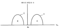
Some EEPROM and flash memory devices have a floating gate that is used to store two ranges of charges so that the memory cell can be programmed / erased between two states (erased state and programmed state). For example, FIG. 1 is a graph showing the distribution of two threshold voltages. The x axis represents the threshold voltage and the y axis represents the number of memory cells. The threshold voltage of the
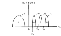
Multi-state flash memory cells are implemented by identifying a plurality of separately allowed threshold voltage ranges separated by forbidden voltage ranges. Each distinct threshold voltage range corresponds to a predetermined value for a set of data bits. 2 illustrates a threshold voltage distribution of a memory cell storing data of two bits of data using four data states. In one embodiment,
As can be seen from FIG. 2, the
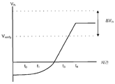
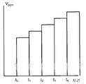
3A shows the programming voltage signal V pgm applied to the control gate as a series of pulses. The magnitude of the pulse is increased by a predetermined step magnitude (e.g. 0.2V-0.4V) for each successive pulse, as represented by ΔV pgm in FIG. 3A. In the period between the pulses, a verify operation is performed. As the number of programmable states increases, the number of verify operations increases, and more time is needed. One means for reducing this time burden is a more efficient verification process, such as disclosed in US Patent Application No. 10 / 314,055, filed December 5, 2002, entitled "Smart Verify For Multi-State Memories." The patent application is hereby incorporated by reference in its entirety. In practice, the pulses of FIG. 3A are each separated by a time interval during verification. However, in order to make FIG. 3 easier to read, the time interval of verification is omitted in the figure.
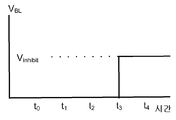
3B shows a voltage signal applied to the bit line of the programmed associated memory cell. 3C shows the threshold voltage of the programmed memory cell. The graph in FIG. 3C is shown smoothly for readability. After each programming pulse, a verify operation (not shown) is performed. During the verify operation, the threshold voltage of the programmed memory cell is checked. If the threshold voltage of a memory cell is greater than the target value (eg, V verify ), programming the memory cell by increasing the bitline voltage from 0v to V inhibit (eg, at t4) is followed by the next cycle. Prohibited from
Like other electronic devices, the consumer requires a memory device that can be programmed as soon as possible. For example, a user of a digital camera storing images on a flash memory card does not want to wait for a long time without needing between the pictures. In addition to programming at a reasonable rate, in order to ensure adequate data storage in a multi-state memory cell, a plurality of ranges of threshold voltages of the multi-state memory cell must be separated from each other with sufficient margin. Only then can the levels of the memory cell be programmed and read in an unambiguous manner. Dense threshold voltage distribution is recommended. In order to obtain a dense threshold voltage distribution, small program steps are generally used, which makes programming the threshold voltage of the memory cell even slower. The denser the desired threshold voltage distribution, the smaller the programming steps and the slower the programming process.
One solution of a method for obtaining dense threshold voltage distributions involves using a two-phase programming process so that the programming process is not delayed without cause. The first phase is a coarse programming phase, in which it is a major concern to increase the threshold voltage in a faster way, and is relatively less interested in dense threshold voltage distributions. The second phase is a fine programming phase, which is a phase that attempts to obtain a dense threshold voltage distribution while increasing the threshold voltage in a slower way to reach the target threshold voltage. Examples of coarse / fine programming are disclosed in US Pat. No. 6,643,188, which is incorporated herein by reference in its entirety.
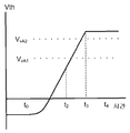
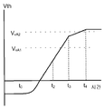
4 and 5 illustrate one embodiment of the coarse / fine programming method in more detail. 4A and 5A show a programming pulse V pgm applied to the control gate. 4B and 5B show bit line voltages of programmed memory cells. 4C and 5C show threshold voltages of programmed memory cells. In the embodiments of FIG. 4 and FIG. 5, two verification levels are used, and V vA1 and V vA2 are shown in the figure . The final target level is indicated by V vA2 . When the threshold voltage of a memory cell reaches V vA2 , the memory cell is prevented from further programming by applying a inhibit voltage to the bit line corresponding to that memory cell. For example, the bit line voltage can be increased up to V inhibit (see FIGS. 4B and 5B). However, when the memory cell reaches a threshold voltage near (or below) the target value, V vA2 , the threshold voltage is subsequently applied by applying a predetermined bias voltage of about 0.3v to 0.8v to the bitline. The programming pulses transition to the memory cell while slowing down. Because the rate of threshold voltage transition decreases during the next few pulses, the final threshold voltage distribution can be narrower than by the method shown in FIG. To implement the method, a second verify level less than the verify level of V vA2 is used. This second verify level is shown as V vA1 in FIGS. 4 and 5. The threshold voltage of the memory cell is V vA1 Greater than but still V vA2 If smaller, the threshold voltage transitioning to the memory cell for subsequent programming pulses will be reduced by applying a bit line bias (V s ) (FIG. 5B). In this case, it should be noted that two verify operations are required for each state. One verify operation verifies the operation corresponding to the final verify level (e.g. V vA2 ) for each state to which coarse / fine programming methods are applied, and the second verifyes the second verify level (e.g. For example, the operation corresponding to V vA1 ) is verified. This may increase the total time required to program the memory cell. In contrast, greater than ΔV pgm Step size can be used to speed up the processes.
4A, 4B and 4C show the operation of a memory cell in which the threshold voltage of the memory cell has passed through V vA1 and V vA2 in one programming pulse. For example, FIG. 4C shows the threshold voltage passing between V vA1 and V vA2 between t 2 and t 3 . Therefore, before t 3 , the memory cell corresponds to the coarse mode. After t 3 , the memory cell corresponds to the inhibit mode.
5A, 5B and 5C illustrate memory cells entering both coarse and fine programming modes. The threshold voltage of the memory cell crosses V vA1 between the times t 2 and t 3 . Before t 3 , the memory cell corresponds to a coarse mode. After t 3 , the bit line voltage is increased to V s , whereby the memory cell is in a fine mode. Between t 3 and t 4 , the threshold voltage of the memory cell crosses V vA2 . Thus, the memory cell is further inhibited from programming by increasing the bit line voltage to V inhibit .
In general, in order to maintain reasonable programming time, coarse / fine algorithms are not applied to the highest memory state (state that corresponds to the largest threshold voltage range). The highest state, such as state C shown by
The technique disclosed herein is intended to more accurately detect threshold voltages of nonvolatile storage elements during programming verification when coarse / fine programming is used.
Coarse / fine programming of nonvolatile memory is provided, where memory cells are at a first rate of programming before they reach a coarse verify level for their intended state. It is programmed and programmed at a second programming speed until the coarse verify level is reached but before the final verify level for their intended state is reached. Large sub-threshold swing factors associated with smaller memory cells can be precisely verified after sensing at the coarse verify level, especially without pre-charging the bitline between different sensinges. When sensing at the level, it can affect the accuracy of the sensing operations. Different reference potentials are used when sensing at the coarse verify level and the final verify level. The difference between the reference potentials can compensate for any discharge of the bit line during coarse level sensing.
One embodiment includes a method of programming a nonvolatile memory. The method includes applying one or more programming pulses to the set of nonvolatile storage elements to program one or more storage elements of the set of nonvolatile storage elements to a particular state. After applying each programming pulse, applying a first voltage to the set of storage elements and comparing the bit line voltage of each of the one or more storage elements with a first reference potential, thereby corresponding to the particular state of the one or more storage elements. Programming to an intermediate verify level is verified. After applying each programming pulse, apply a second voltage to the set of storage elements and compare the bit line voltage of each of the one or more storage elements with a second reference potential to thereby achieve the particular state of the one or more storage elements. Verification of programming to the corresponding final verify level is performed. Here, the second reference potential compensates for the reduction in the bit line voltage of each of the one or more storage elements resulting from verification of programming to the intermediate verify level.
In another embodiment, a method is disclosed for verifying programming of nonvolatile storage, the method comprising: charging a bitline corresponding to a nonvolatile storage element; Applying an intermediate verify voltage corresponding to a target state for the nonvolatile storage element; Sensing the voltage on the bit line while the intermediate verify voltage is applied; Comparing the voltage on the bit line with a first reference potential; Applying a final verify voltage corresponding to the target state for the nonvolatile storage element to the nonvolatile storage element; Sensing the voltage of the bit line while the final verify voltage is applied and because the bit line is completely discharged from the charged state; And comparing the voltage of the bit line with a second reference potential while the final verify voltage is applied.
One exemplary embodiment includes a set of nonvolatile storage elements and management circuitry in communication with the set of nonvolatile storage elements. The one or more management circuits may perform the processes described above.
The present invention can more accurately sense the threshold voltages of nonvolatile storage elements during programming verification when coarse / fine programming is used.
1 is a graph showing two threshold voltage distributions.
2 is a graph showing four threshold voltage distributions.
3A, 3B and 3C illustrate a programming process. 3A illustrates a programming voltage signal applied to the control gate of the nonvolatile storage element. 3B shows the voltage signal applied to the bit line for the NAND string. 3C shows the threshold voltage of the nonvolatile storage element to be programmed.
4A, 4B, and 4C illustrate one embodiment of a programming process performed as part of coarse / fine programming.
5A, 5B, and 5C illustrate one embodiment of a programming process performed as part of coarse / fine programming.
6 is a plan view of a NAND string.
FIG. 7 is an equivalent circuit diagram of the NAND string of FIG. 6.
8 is a block diagram of one embodiment of a nonvolatile memory system.
9 shows an example of a configuration of a memory array.
10 illustrates a program voltage signal including verify pulses, which may be used according to one embodiment.
11 is a flowchart illustrating a method of programming a nonvolatile memory, according to an exemplary embodiment.
12 shows an example of a set of threshold voltage distributions and a full sequence programming process.
13 shows an example of a set of threshold voltage distributions and a two-pass programming process.
14A-14C show an example of a set of threshold voltage distributions and another two-pass programming process.
15 is a timing diagram illustrating various signals that may be applied to a memory device during a program and program verify operation.
16 is a graph showing the bit line potentials of different memory cells during a verify operation in which the memory cells have small sub-threshold swing factors.
17 is a graph showing the bit line potentials of different memory cells during a verify operation in which the memory cells have large sub-threshold swing factors.
18 is a graph illustrating bit line potentials of different memory cells during a verify process according to one embodiment.
19 is a flowchart illustrating verification of memory cells during coarse / fine programming, according to one embodiment.
20 is part of a column control circuit of a memory device that may be used in accordance with one embodiment.
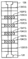
One embodiment of a flash memory system suitable for implementing an embodiment of the present invention utilizes a NAND structure, which comprises a plurality of transistors in series arranged between two select gates. The series transistors and the select gates are referred to as a NAND string. 6 is a plan view showing one NAND string, and FIG. 7 is an equivalent circuit diagram thereof. The NAND string shown in FIGS. 6 and 7 includes four
Although FIGS. 6 and 7 show four memory cells in a NAND string, using these four transistors is presented by way of example only. The NAND string may have four or fewer memory cells or four or more memory cells. For example, certain NAND strings may include eight, sixteen, thirty-two memory cells, and the like. The number of memory cells of the NAND string in the present description is not limited to a specific number.
Suitable embodiments related to NAND type flash memories and their operation are described in US Pat. No. 5,570,315; US Patent No. 5,774,397; US Patent No. 6,046,935; US Patent No. 5,386,422; US Pat. No. 6,456,528 and US Patent Application No. 09 / 893,277 (published US 2003/0002348), all of which are incorporated herein by reference in their entirety. Information about programming a NAND flash memory, including a self boosting technique, was filed on March 5, 2003, entitled U.S. Patent Application No. 10 / 379,608 and See US Patent Application No. 10 / 629,068, filed on July 29, 2003, entitled "Detecting Over Programmed Memory," which is incorporated by reference in its entirety. Of course, other types of flash memory devices can also be used with the present invention. For example, US Pat. Nos. 5,095,344, 5,172,338; 5,890,192 and 6,151,248 disclose NOR type flash memories, which are incorporated by reference in their entirety. Another embodiment of a flash memory type can be found in US Pat. No. 6,151,248, which is incorporated herein by reference in its entirety.
The technique described herein is not limited to floating gate type memories. For example, the techniques described herein employ various types of charge storage regions / layer (s) between a control gate (or wordline) and a substrate, such as non-conductive, known as nano-crystals. It can be used with memory devices using dielectric charge storage regions or small silicon islands.
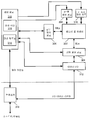
8 is a block diagram illustrating one embodiment of a flash memory system that may be used to practice one or more embodiments of the present invention. 8 is exemplary because other systems and embodiments may be used. The
Data stored in the memory cells is read by the
Command data for controlling the flash memory device is input to the controller 218. The command data informs the flash memory of what action is required. The input command is sent to a
The
One example memory system includes one integrated circuit that includes a
In some embodiments, some components of FIG. 8 may be combined. In various designs, one or more components of FIG. 8 other than
9, one embodiment of a
In the embodiment of FIG. 9, each block has 8,512 columns divided into even columns and odd columns. The bit lines are also divided into even bit lines BLe and odd bit lines BLO. In odd / even bitline architectures, memory cells that follow a common wordline and are connected to an odd bitline are programmed in one time, while memory cells that follow a common wordline and are connected to an even bitline may be stored at different times. programmed another time). Although four cells shown in each NAND string of FIG. 9 are included, more than four or less than four memory cells may be used. One end of the NAND string is connected to a corresponding bit line through a first select transistor connected to a drain select gate control line (SGD), and the other end is connected through a second select transistor connected to a source select gate control line (SGS). Is connected to the C-source.
In another embodiment, the bit lines are not divided into odd and even bit lines. Such architectures are commonly referred to as all bit line architectures. In all bitline architectures, all bitlines of a block are selected simultaneously during read and program operations. Memory cells that follow a common wordline and are connected to any bitline are programmed simultaneously.
During one embodiment of read and program operations in odd / even bitline architectures, 4,256 memory cells are selected simultaneously. The selected memory cells have the same word line and the same kind of bit line (eg, even bit lines or odd bit lines). Thus, 532 bytes of data can be read or programmed simultaneously. The 532 bytes of data read or programmed simultaneously form a logical page. Thus, one block can store at least eight logical pages (four word lines, each with odd and even pages). If each memory cell stores two bits of data (e.g., multi-state memory cells), each of the two bits is stored in a different page, and one block stores 16 logical pages. According to the present invention, blocks or pages of different sizes may be used. In addition, architectures other than those shown in FIGS. 8 and 9 may also be used for the practice of the present invention.
Memory cells can be erased by increasing the erase voltage of the p-well (eg, 20 volts) and grounding the word lines of the selected block. The source and bit lines are floating. Erasing may be performed in the entire memory array, in a separate block, or in another unit of cells. Electrons are transferred from the floating gate to the p-well region and the threshold voltage is negative (in one embodiment).
In one embodiment, when programming the memory cell, the control gate receives a series of programming pulses of increasing magnitude, while the drain and p-well receive zero volts. In one embodiment, the magnitude of the series of pulses ranges from 12 volts to 24 volts. In other embodiments, the range of series of pulses may be different, for example having a starting level higher than 12 volts. During programming of the memory cells, a verify operation is performed in the period between the programming pulses. That is, the programming level of each cell of the group of cells programmed in parallel is read between each programming pulse to determine whether the verify level to be programmed has been reached or exceeded the verify level to be programmed. One way to verify the programming is to check for continuity at a particular comparison point. Cells verified to be sufficiently programmed, for example, in NAND cells, set the bitline voltage from 0 to V DD (e.g., 2.5V) for all subsequent programming pulses to terminate the programming process for those cells. Looked out by increasing. In some cases, the number of pulses will be limited (
10 illustrates a program voltage signal according to an embodiment. This signal has a set of pulses of increasing magnitude. The magnitude is increased by a predetermined step size for each pulse. In one embodiment including memory cells storing multiple bit data, an exemplary step size is 0.2 volts (or 0.4 volts). There are verify pulses between each program pulse. The signal of FIG. 10 assumes four state memory cells, and thus includes three verify pulses. For example, there are three sequential verify pulses between
11 is a flowchart illustrating one embodiment of a method of programming a nonvolatile memory. The memory cells to be programmed are erased in
Triggered by a “program” instruction, the data latched in
In
If at
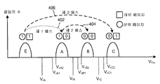
At the end of a successful program process, the threshold voltages of the memory cells should preferably be within one or more threshold voltage distributions for programmed memory cells or within the threshold voltage distribution for erased memory cells. 12 shows a threshold voltage distribution for a memory cell when each memory cell stores two bits of data. 12 shows a first threshold voltage distribution E for erased memory cells. Three threshold voltage distributions A, B and C for programmed memory cells are also shown. In one embodiment, the threshold voltages in the E distribution have negative values, and the threshold voltages in the A, B, and C distributions have positive values.
Each distinct threshold voltage range of FIG. 12 corresponds to predetermined values for the data bit set. The specific relationship between the data programmed into the memory cell and the threshold voltage levels of the cell depends on the data encoding scheme adopted for the cells. In one embodiment, data values are specified in a threshold voltage range using gray code assignment to ensure that only one logic bit is affected even if the threshold voltage of the floating gate has incorrectly transitioned to a physical state adjacent to the threshold voltage. to be. However, in other embodiments gray coding is not used. An example is "11" in threshold voltage range E (state E), "10" in threshold voltage range A (state A), and "00" in threshold voltage range B (state B). And " 01 " to the threshold voltage range C (state C). Although FIG. 12 shows four states, embodiments in accordance with the present invention may include other multi-state structures that include more or less than four states.
12 also shows an embodiment using full sequence programming. In full sequence programming, memory cells can be programmed directly from the erase state E to any of the program states A, B or C. For example, a population of memory cells to be programmed is first erased, so that all memory cells in the population are in an erased state (E). The process shown in FIG. 11 using a series of program voltage pulses applied to the control gate of selected memory cells will be used to program the memory cells directly into states A, B or C. While some memory cells are programmed from state (E) to state (A), other memory cells are programmed from state (E) to state (B) and / or state (E) to state (C).
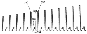
Figure 13 shows an example of a two-pass technique for programming multi-state memory cells that store data in two different pages (lower page and upper page). Four states are shown (state E (11), state A (10), state B (00) and state C (01)). In state E, both pages store "1". In state A, the lower page stores "0" and the upper page stores "1". In state B, both pages store " 0 ". In state C, the lower page stores "1" and the upper page stores "0". Note that although specific bit patterns are assigned to each state, other bit patterns may also be assigned. In the first programming pass, the threshold voltage level of the cell is set according to the bit to be programmed in the lower logical page. If the bit is " 1 ", the threshold voltage does not change since the threshold voltage is in the proper state as a result of previously erasing. However, if the bit to be programmed is "0", the threshold level of the cell is increased to state A, as shown by
In the second programming pass, the threshold voltage level of the cell is set according to the bit being programmed in the upper logical page. If the upper logical page bit stores " 1 ", then any programming is done because the cells are all in one of the states (E or A) performing the upper page bit " 1 " according to the programming of the lower page bit. Also does not occur. If the upper page bit is going to be a logic "0", the threshold voltage is transitioned. If the first pass occurred in a cell in the erased state E, the cell is programmed in the second mode, as shown by
Figures 14A-14C disclose another process for programming non-volatile memory, which, for any particular memory cell, writes that particular memory cell with respect to a particular page after writing adjacent memory cells for previous pages. By writing, the floating gate to floating gate coupling is reduced. In one embodiment of the process taught by FIGS. 14A-14C, nonvolatile memory cells store two bits of data per memory cell using four data states. For example, assume that state E is an erased state and states A, B and C are program states. State E stores data 11. State
In one embodiment, after a memory cell is programmed from state E to state B, adjacent memory cells of the memory cell of the NAND string will be programmed for the lower page of the memory cell. For example, referring back to FIG. 7, after the lower page of the
14C shows a process for programming a higher page. If the memory cell is in the erase state E and the upper page remains 1, the memory cell will remain in the state E. If the memory cell is in state E and its upper page data is programmed to zero, then the threshold voltage of the memory cell will be increased so that the memory cell is in state A. If the memory cell was in the middle threshold voltage distribution 320 and the upper page data remained at 1, the memory cell would be programmed to the final state B. If the memory cell is in the intermediate threshold voltage distribution 320 and the upper page data becomes data zero, the threshold voltage of the memory cell will be increased to keep the memory cell in state (C). Since only upper page programming of adjacent memory cells will affect the apparent threshold voltage of a given memory cell, the process shown in FIGS. 14A-14C reduces the coupling effect between floating gates.
Although FIGS. 14A-14C provide an example for four data states and two pages of data, the idea taught by FIGS. 14A-14C is more or less than four states and has a different number of pages. It may be applied to other embodiments.
12, 13 and 14A to 14C show read reference voltages, V rA , V rB and V rC for reading data from memory cells. By checking whether the threshold voltages of a given memory cell are above or below V rA , V rB and V rC , the system can determine which state the memory cell is in. Cells conducting the applied control gate voltage (V cg) of the V rA is in state (E), V conduction cells in V rB non-rA is in the state (A), conductive in the V rC than the V rB The cell to be in is in state B, and the cell which is not conducting in V rA , V rB or V rC is in state C.
In read and verify operations, the select gates of the selected block are increased to one or more select voltages, and unselected word lines (e.g., WL0, WL2, and WL3) to operate the transistor as pass gates. The read pass voltage V read is increased to 4.5 volts, for example. Source and p-well are at 0 volts. The selected word line BLe is precharged to a level of, for example, 0.7V. The selected word line (e.g., WL1) is connected to a read or verify voltage, where each read and verify operation is performed to determine whether the level of the read or verify voltage is above or below this level. Is specified in. If the threshold voltage is higher than the read or verify level on the word line, the potential level of the bit line BLe associated with the cell of interest remains at a high level because of the non-conductive memory cell. On the other hand, when the threshold voltage is lower than the read or verify level, due to the conductive memory discharging the bit line, the potential level of the associated bit line BLe decreases to a lower level, for example less than 0.5V. Thus, the state of the memory cell is detected by a voltage comparator sense amplifier connected to the bit line to sense the resulting bit line voltage.
The above erase, read and verify operations are performed according to the prior art. Accordingly, many of the details described can be modified by one skilled in the art. Other erase, read, and verify operations of the prior art can also be used.
12, 13 and 14A-14C also show verify voltages including V vA2 , V vB2 and V vC2 . When programming the memory cells to state A, the system will check whether the memory cells have threshold voltages greater than or equal to V vA2 to verify that the memory cells have reached their final target level. When programming the memory cells to state B, the system will check whether the memory cells have threshold voltages greater than or equal to V vB2 to verify that the memory cell has reached its final target level. When programming the memory cells to state C, the system checks V vC2 to verify that the memory cells have reached their final target level. We will check whether we have threshold voltages greater than or equal to.
As described above, coarse / fine programming uses two sets of verify voltages for one or more of the programmable states. This is to verify the final level of programming for the memory cell and additionally switch the cells from the coarse programming mode to the fine programming mode when the cell is nearing the final verify level for its intended state but has not yet reached. Two sets of verify levels in FIGS. 12, 13 and 14A-14C are shown for each programmed state. Verify levels V vA2 , V vB2 and V vC2 are used to verify that the memory cell has reached the final verify level for its intended state, while verifying that the memory cell has reached the coarse verify level. Verification levels V vA1 , V vB1 and V vC1 are used for this purpose . Cells that have not reached any of the verify levels for their intended state undergo full or coarse programming during the next iteration of the programming process. Cells that reach the coarse verify level but not the final verify level for that intended state undergo reduced or fine level programming during the next programming iteration. Cells whose intended state has reached the final verify level are prohibited from programming during the next programming iteration. Although two sets of verify levels represent respective programmable states in FIGS. 12, 13 and 14A-14C, some embodiments may not use the coarse verify level for one or more states. For example, some embodiments will not use coarse verify levels for the best programmable state since there is no higher state that must be different during reading. Such embodiments are contemplated.
FIG. 15 is a timing diagram illustrating various signals applied to a nonvolatile memory device during part of an example programming process including coarse / fine programming. FIG. The first time period, labeled "programming", includes signals applied to program one or more memory cells of the selected word line WL_sel. This programming period is generalized and may correspond to a first programming pulse or a second or subsequent programming pulse applied to a wordline. This period corresponds to step 360 of FIG. This programming cycle begins by increasing the source line to a low positive voltage, about 1V. The drain select gate is then opened (or turned on) by applying V SG (eg, 3.5V) to the drain select gate line SGD. After opening the drain select gate, the inhibit voltage V inhibit is applied to any unselected word lines. In FIG. 15, an odd / even program technique or architecture is estimated. The bit line BLn represents the selected bit line. Therefore, adjacent bit lines (BLn + 1, BLn + 3, etc. and BLn-1, BLn-3, etc.) of the block will not be selected during the programming operation. In general, all bit lines (e.g., odd or even) are simultaneously read and programmed so that all bit lines (BLn, BLn + 2, etc.) receive the same signals applied to BLn.
The unselected bit lines are increased to the inhibit voltage V inhibit so that the unselected bit lines remain at the inhibit voltage V inhibit throughout the first programming period. The selected bit line BLn is set or biased according to the data to be programmed into the memory cell of the word line selected at that particular bit line. If the memory cell of bit line BLn should be inhibited from programming, BLn is increased to voltage level V inhibit . In one embodiment, V inhibit is equal to V DD (eg, 1.8V-3.3V). If the memory cell of the bit line BLn is enabled for full or coarse programming, the BLn is increased to the enable voltage V enable . In one embodiment, V enable is equal to ground or 0V. If the memory cell of the bit line BLn has reached the coarse verify level for the state to be programmed but has not reached the final verify level for that state, the bit line is increased to the intermediate level V S. In one embodiment, V S is approximately equal to 2.0V. The value of V S may vary from embodiment to embodiment and depends on the level of V inhibit and other device characteristics. The
After biasing each selected bitline according to the amount of programming to be applied to the memory cell of each selected bitline, the wordlines are biased. Unselected word lines, denoted WL_unsel, are increased to pass voltage (V pass ). This voltage V pass enables boosting of the NAND string channel to NAND strings with memory cells that are prohibited from programming during this programming period. The selected word line WL_sel is also increased to voltage V pass to enable boosting of channels for NAND strings containing memory cells at WLn that will not undergo programming. After increasing each word line to the V pass level, the selected word line is increased to the program voltage pulse level V pgm1 . After applying a programming pulse to the selected word line, the word lines are reduced to 0V. After reducing the word lines to 0V, the unselected and selected bit lines are each reduced to 0V. The drain side select gate is then turned off by applying 0V to the drain select gate line SGD. The programming period is completed by reducing the source line voltage from 1V to 0V.
After applying the voltage pulse V pgml of FIG. 15, a verify operation following the first programming period is started. As shown in FIG. 15, the verify operation is divided into coarse level verification and fine level verification. The coarse level verification begins by precharging the bit line BLn (along with each other selected bit line) to a predetermined voltage level V clamp . V clamp is equal to about 0.7V in one embodiment. Once the bit line is precharged, the word lines are biased for coarse level sensing. The read pass voltage V read is supplied to the unselected word lines. This V read is a pass voltage that ensures that unselected memory cells are turned on or conductive during the verification process regardless of the state in which the unselected memory cells are programmed. This allows verification of the memory cells just at the word line WL_sel. While V read is applied to unselected word lines, a coarse level verify voltage V v1 is supplied to the selected word line. After applying the appropriate bias states to each word line, both the drain side select gate and the source side select gate are turned on by applying V SG to the drain select gate line SGD and the source select gate line SGS. It should be noted that the generalized description in FIG. 15 is provided regardless of any particular state. Therefore, V v1 may correspond to a coarse verify level for state A, state B, state C, or other state.
After precharging the selected bit lines, biasing the word lines, and turning on the select gates, the selected bit lines can freely discharge according to the state of the memory cell of the bit line connected to the selected word line WL_sel.
In the embodiment of FIG. 15, the bit lines are not precharged again after coarse level verification. The selected word line is increased directly from the coarse verify level to the final or fine verify level V v2 . Like the coarse verify level, V v2 represents a general description and may include the final verify level for state (A), state (B), and the like. This technique enables efficient verification by eliminating the time required to precharge selected bitlines. This also eliminates the need to produce energy to recharge the bitlines. After applying the final verify level V v2 to the selected word line, the selected bit lines will be discharged according to the state of the memory cell at the word line WL_sel.
The bit line voltage is sensed again after a predetermined amount of time following the application of V v2 . This predetermined amount of time may be represented or set as a period of time following the opening of the selection gate or a period of time following the application of the final verify level during coarse level sensing. The sensed voltage is compared with the reference potential V sense . If the bit line voltage is V sense If not discharged below, the memory cell is determined to have a threshold voltage above the final verify level V v2 . If the bitline is V sense When discharged below, the memory cell is determined to have a threshold voltage below the final verify level V v2 . After sensing, the selected bit lines are reduced to 0V and then the word lines are reduced to 0V. The drain and source select gate lines are then reduced to 0V to complete the precision verification process.
If a multi-state memory device is used, the coarse level verification and fine level verification processes will be repeated as many times as necessary for the corresponding states. For example, a four state device may need the performance of coarse and fine level verifications three times-once at A state verify levels, once at B state verify levels, and once at C state verify levels. After completing the fine level verification for the A state, the bitline is precharged again and the process repeats. After completing the fine level verification for the B state, the bitline will be precharged again to begin the coarse level verification for state C. Some embodiments may not sense at each state verify level during each process. For example, reading the immediately upper page data of memory cells as shown in FIG. 13 only requires sensing at state B verify levels.
Figure 15 shows an additional iteration of the programming process that can be used to further program memory cells that have not yet reached their final verify levels after increasing the source potential to 1V. The drain side select gate is turned on by applying V SG to the drain source select gate line SGD. Unselected bit lines BLn + 1 / BLn-1 are increased to V inhibit . The selected bit line BLn is then biased according to the results of the previous verify operation and the data programmed into the selected bit line. The arrows shown in FIG. 15 indicate the corresponding bit line voltage levels applied during the next programming iteration. The memory cell that discharged the bit line under application of the coarse verify level (dotted line 454) is supplied with an enable voltage (V enable ) to allow the memory cell to undergo full programming during the next iteration. A memory cell that has not discharged a bit line under a coarse verify level or a final verify level (solid line 450) represents a memory cell that has reached its final verify level. Thus, the bit line of the memory cell is biased at V inhibit . Memory cells that have not discharged the corresponding bitline under the coarse verify level but have discharged the bitline under the final verify level are increased to an intermediate voltage level (Vs) so that they can undergo fine programming during the next programming iteration.
After biasing each selected bit line, the unselected and selected word lines are increased to their pass voltage levels (V pass ). The selected word line is then ramped to the second programming voltage pulse level V pgm2 . The second pulse is generally increased by the step size V pgm than the preceding pulse. After applying V pgm2 , the word lines are recovered down to 0V. Selected and unselected bit lines are also restored down to 0V and drain select gates are turned off. And the source line potential is lowered to 0V. It is again noted that the embodiment shown in FIG. 15 represents only part of the programming and verification process in a typical implementation. One or more program voltage pulses may be applied to program each selected memory cell to a target level with coarse and fine level verification at appropriate levels performed between the application of each pulse.
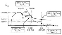
FIG. 16 is a graph showing more detail of coarse level and fine level sensing operations for a particular state such as may be performed in FIG. 15 and during
The bit lines for the memory cells are precharged to a predetermined level (V clamp ). A coarse verify level V v1 (eg, V cg = V vB1 ) is applied to the selected word line. The drain select gates are then turned on to connect each NAND string to a bit line of the NAND string. As shown in FIG. 16, the bit lines will experience some discharge even if each memory cell has a threshold voltage above the coarse verify level. Despite the application of the control gate voltage V cg lower than the threshold voltage of the bit lines, transistor-based memory cells will still conduct some amount of current between the source and drain of the bit lines. In particular, memory cells fabricated in modern devices of small size are not placed in an absolute off condition under the application of positive gate bias. The extent to which the transistor conducts current at an applied gate voltage below its threshold voltage is indicated by the device's sub-threshold swing factor (S-factor).
In general, commercially manufactured memory cells exhibit low sub-threshold step factors. 16 illustrates a memory device having a low sub-threshold swing factor such that the memory cell does not conduct a significant amount of current under an applied control gate voltage, which is less than the threshold voltage of the memory cell. Even when the gate voltage is below the threshold voltage, the threshold voltage of the memory cell will naturally affect the level of conduction. Thus, the memory cell of FIG. 16 having a threshold voltage just above the final verify level (solid line 460) discharges in a smaller amount than the memory cell having a threshold voltage just below the final verify level (dashed line 462).
After a predetermined amount of time following the drain select gate being opened, the sensing operation is performed at the coarse verify level. The bit line voltage is sensed and compared to the reference potential (V sense ). For all of the cells shown in FIG. 16, it is determined that the bit line voltage V BL is greater than the sense voltage V sense during coarse level sensing. Thus, the sense amplifier determines that each memory cell has a threshold voltage above the coarse verify level (V v1 ).
After sensing at the coarse verify level, the final verify level is applied to the selected word line. The control gate of each memory cell is supplied with a final verify voltage V v2 (eg, V cg = V vB2 ). Memory cells with threshold voltages above the final verify level are not turned on, so that the cell's bitline voltage does not discharge in significant amounts under application of the final verify level. Again, the bit line voltage will discharge to some extent because of the sub-threshold swing factor, but the discharge is not significant enough to affect the accuracy of the sensing. Memory cells having a threshold voltage below the final verify level (V v2 ) are turned on and conductive under application of the final verify level. Thus, the bit line of this memory cell discharges to a significant amount of the final verify level applied.
After a predetermined amount of time following the application of the final verify level, the bit line voltage of each memory cell is sensed. Again, this predetermined time can be established with respect to the opening of the drain select gate for coarse level sensing or with respect to the application of the final verify voltage. The memory cell indicated by
17 is a graph illustrating a memory device having a large sub-critical swing factor. Again, the memory cell with the threshold voltage just above the final verify level is indicated by the
After detecting the coarse level, the selected word line is supplied with the final verify level V v2 . Memory cells having a threshold voltage just above the final verify level (solid line 460) are not as conductive as those having a threshold voltage just below the final verify level (dashed line 462). However, as shown in Figure 17, the large S-factor associated with the memory causes the bit line voltage of a memory cell with a threshold voltage above the final verify level to discharge below V sense . A memory cell with a threshold voltage below the final verify level also discharges its bitline below V sense as expected. During fine level sensing, a sense amplifier for a memory cell having a threshold voltage above the final verify level determines whether the cell's bitline has discharged below V sense . Thus, the sense amplifier determines whether the memory cell has a threshold voltage below the final verify level. This indicates an error in the sensing operation. The sense circuit will erroneously determine that the memory cell is not yet programmed to its final target level and will cause the cell to undergo other programming. The memory cell indicated by the dotted line also has a sensed bit line voltage below V sense . The sense amplifier for this cell accurately determines that the cell's threshold voltage is below the final verify level (V v2 ).
18 is a graph of a coarse and fine verification and detection method in accordance with an embodiment of the present invention that can handle bitline discharges resulting from large S-factor devices.
After sensing at the coarse verify level, the selected word line is supplied with a final verify level (V v2 ). Again, memory cells with threshold voltages above the final verify level will conduct significant amounts of current due to the large S-factor of the device. Memory cells with threshold voltages below the final verify level are more conductive as expected and discharge a significant amount of bit lines in the memory cells.
After a predetermined amount of time, the bit line voltage of each memory cell is sensed and compared with a reference potential. During the precision level sensing, different reference potentials are used. The sensed bit line voltage is compared with the final reference potential V sense2 . V sense2 is V sense1 Lower than The lower reference potential compensates for the bitline discharges that occur under application of the coarse verify level. This compensation takes into account the large S-factor associated with the memory device causing the memory cells to discharge the bit lines of the memory cells to some significant amount, even when the memory cells have threshold voltages above the verify level. In FIG. 18, the memory cell having the threshold voltage just above the final verify level has the sensed bitline voltage of the memory cell compared to V sense2 . In this case, the sense amplifier will determine that the bit line voltage is greater than the final reference potential V sense2 . Thus, the sense amplifier will accurately determine that the threshold voltage of the memory cell is greater than the final verify level V v2 . For a memory cell having a threshold voltage just below the final verify level, the sense amplifier compares the sensed bit line voltage with the final reference potential V sense2 . The sense amplifier for this cell's bitline will determine that the bitline voltage is less than the final reference potential, V sense2 . The sense amplifier will again accurately determine that the memory cell has a threshold voltage below the final verify level (V v2 ). Thus, by adjusting the level of the reference potential between coarse level verification and fine level verification when the bit line is not precharged again between each sensing operation, a more accurate sense of the state of the memory cell is achieved. The difference in the reference potentials provides compensation for the amount of discharge during coarse level verification.
In one embodiment, the final reference potential V sense2 has a threshold voltage above the coarse verify level V v1 when V v1 is applied to the word line of the memory cell during the coarse level sensing than the intermediate reference potential V sense1 . The amount of the bit line voltage for the memory cell having is as small as the expected discharge. Memory cells that are theoretically nonconductive under the applied verify level will have an associated bitline voltage discharge resulting from the large S-factor of the device. The difference between the intermediate and final V sense levels can be set approximately to the difference between the bitline precharge level and the bitline voltage that occurs when a coarse verify level is applied to the wordline. In this way, the final reference potential V sense2 compensates for the bitline discharge resulting from the large S-factor device. Depending on the requirements of certain implementations, other values of intermediate reference potential V sensel and final reference potential V sense2 may be used. For example, V sense2 may be set smaller than V sensel by an amount less than the expected discharge of the bitline for the memory cell when a coarse verify level is applied to the wordline. The smaller offset of V sense2 relative to V sense1 can still accommodate the level of bitline discharge during coarse level sensing. In one embodiment, the intermediate reference potential V sense1 is a general V sense that can be used when the devices have an average or lower S-factor. Approximately the same level. In this case, the final reference potential V sense2 is adjusted with reference to V sense1 by an amount that can compensate for the reduction in the bitline during coarse level sensing.
In one embodiment, the memory array undergoes testing during the manufacturing process. Such tests may include characterization of memory array performance. For example, when a coarse verify level is applied to a word line and the threshold voltage of the memory cell is above this coarse verify level, the memory array can be measured to determine the amount that the bit lines will discharge. In one embodiment, the amount of discharge associated with multiple bit lines of the device may be averaged to reach an appropriate amount. During the manufacturing process, the value of V sense2 can be set for V sense1 to accommodate the measured reduction in bitline voltage under application of coarse verify levels. In addition, the intermediate reference potential V sense1 may be based on the characterization of the memory device. In some embodiments, a selected subset of memory devices can be checked and characterized, and the results of the characterization are used to set V sensel and V sense2 for a larger set of devices including the subset's characterized results. In other embodiments, the fabrication process can set the levels of V sensel and V sense2 for each memory device based on testing and characterization for that particular memory device. It is also possible to set a time period between turning on the select gate and performing coarse level sensing to optimize accuracy in coarse level sensing. Similarly, the time period between applying the final verify level to the selected word line and sensing at that level can be selected based on testing and characterization to further provide accurate sensing at both levels. As mentioned above, the time before sensing during coarse level sensing may be set for the time during which select gates are turned on during coarse level sensing or for the time during which the fine verify level is applied to the selected wordline. Various techniques can be used to set these values after characterization. For example, a set of anti-fuses, electrically programmable fuses, etc. may be provided within the memory device to store data regarding the operation of the device. These fuses can be set to store data indicating values of V sense and / or time periods for sensing.
19 is a flow diagram illustrating a process for verifying the programming of one or more cells. In one embodiment, the process of FIG. 19 is performed at
In
Steps 502-528 of FIG. 19 may be repeated for the number of verify operations that need to be performed depending on the number of potential states of the memory device. The verification of
20 shows a portion of the
The foregoing detailed description of the invention is provided to describe and describe the invention in detail. It is not intended to be exhaustive or to limit the invention to the precise form disclosed. Many modifications and variations are possible in light of the above teaching. The embodiments described herein are chosen to best illustrate the principles of the present invention and the practical application of the present invention, which are best suited to various embodiments and various modifications as are suited to the particular use contemplated by the person skilled in the art. These are the ones that are chosen for the purpose of describing. It is intended that the scope of the invention be defined by the claims appended hereto.
302: memory cell array
304: column control circuit
306: low control circuit
308: p-well control circuit
310: c-source control circuit
312: Data I / O Buffer
314: command circuit
315: control circuit
316: state machine
318: controller
Claims (20)
Applying one or more programming pulses to the set of nonvolatile storage elements to program one or more storage elements of the set of nonvolatile storage elements to a particular state;
After applying each programming pulse, applying a first voltage to the set of storage elements and comparing the bit line voltage of each of the one or more storage elements with a first reference potential to a medium verify level corresponding to the particular state. Verifying programming of said one or more storage elements of;
After applying each programming pulse, applying a second voltage to the set of storage elements and comparing the bit line voltage of each of the one or more storage elements with a second reference potential to a final verify level corresponding to the particular state. Verifying programming of said one or more storage elements of;
Wherein the second reference potential compensates for a reduction in the bit line voltage of each of the one or more storage elements resulting from verification of programming to the intermediate verify level.
The second reference potential is a level for compensating for a decrease in the bit line voltage of each of the one or more storage elements resulting from verification of programming to the intermediate verify level when the one or more storage elements are above the intermediate verify level. Method for programming a nonvolatile memory, characterized in that provided.
The second reference potential is equal to the first reference by an amount that is substantially equal to an amount to which the bit line of the one or more nonvolatile storage elements is discharged when the first voltage is applied and the one or more storage elements are above the intermediate verify level. A method of programming a nonvolatile memory, characterized in that it is less than a potential.
And wherein said second reference potential is less than said first reference potential by an amount substantially equal to an amount of bitline discharge for a storage element above said intermediate verify level when said first voltage is applied. How to program memory.
Pre-charging the set of bitlines in communication with the one or more storage elements after applying each programming pulse and prior to verifying programming to the intermediate verify level;
Verifying programming to the intermediate verify level comprises:
Opening a set of select gates in communication with the set of bit lines and the one or more storage elements; And
Sensing a bit line voltage of each of the one or more storage elements after a predetermined amount of time subsequent to opening the set of select gates,
Verifying programming to the final verify level comprises sensing a bitline voltage of each of the one or more storage elements after another predetermined amount of time subsequent to opening the set of select gates. A method of programming a nonvolatile memory, characterized by the above-mentioned.
The set of nonvolatile storage elements is in communication with a first wordline; And
And the set of bit lines includes every other bit line in the group of bit lines.
Precharging a set of bitlines in communication with the one or more storage elements after applying each programming pulse and prior to verifying programming to the intermediate verify level,
Verifying programming to the final verify level does not include precharging the set of bit lines after verifying programming to the intermediate verify level.
And wherein said set of bit lines includes bit lines every other in a group of bit lines.
Applying one or more additional programming pulses to the set to program one or more other storage elements of the set to a different state; And
After applying each additional programming pulse, verifying programming of the one or more storage elements to another final verify level corresponding to the different state,
Wherein the other final verify level is higher than the intermediate verify level and the final verify level for the particular state.
And said intermediate verify level is a coarse verify voltage.
Management circuitry in communication with the set of storage elements,
Here, the management circuit,
Apply one or more programming pulses to the set to program one or more storage elements of the set to a specific state;
After applying each programming pulse, the management circuit corresponds to the particular state by applying a first voltage to the set of storage elements and comparing the bit line voltage of each of the one or more storage elements with a first reference potential. Verify the programming of the one or more storage elements to an intermediate verify level;
After applying each programming pulse, the management circuit corresponds to the particular state by applying a second voltage to the set of storage elements and comparing the bit line voltage of each of the one or more storage elements with a second reference potential. Verify programming of the one or more storage elements to a final verify level;
Wherein the second reference potential compensates for a reduction in the bit line voltage of each of the one or more storage elements resulting from verification of programming to the intermediate verify level.
The management circuit is configured such that when the one or more storage elements are above the intermediate verify level, the management circuit is at a level to compensate for a reduction in the bit line voltage of each of the one or more storage elements resulting from verification of programming to the intermediate verify level. And provide a second reference potential.
The second reference potential is equal to the first reference by an amount that is substantially equal to an amount to which the bit line of the one or more nonvolatile storage elements is discharged when the first voltage is applied and the one or more storage elements are above the intermediate verify level. Non-volatile memory system, characterized in that less than the potential.
And wherein said second reference potential is less than said first reference potential by an amount substantially equal to an amount of bitline discharge for a storage element above said intermediate verify level when said first voltage is applied. Memory system.
A set of bitlines in communication with the one or more storage elements and the management circuitry; And
Further comprising a set of select gates in communication with the set of bit lines and the one or more storage elements,
The management circuitry precharges the set of bit lines after applying each programming pulse and before verifying programming to the intermediate verify level;
The management circuit verifies programming to the intermediate verify level by opening the set of select gates, and bitlines each of the one or more storage elements after a predetermined amount of time subsequent to opening the set of select gates. Sense a voltage; And
The management circuitry verifies programming to the final verify level by sensing a bitline voltage of each of the one or more storage elements after a different predetermined amount of time subsequent to opening the set of select gates. Nonvolatile Memory System.
Further comprising a first wordline in communication with the set of nonvolatile storage elements,
And the set of bit lines includes a bit line every other in the group of bit lines.
Further comprising a set of bitlines in communication with the one or more storage elements,
The management circuit precharges the set of bit lines after applying each programming pulse and before verifying programming to the intermediate verify level,
And the management circuitry does not precharge the set of bit lines after verifying programming to the intermediate verify level to verify programming to the final verify level.
And the set of bit lines includes a bit line every other in the group of bit lines.
And wherein said set of nonvolatile storage elements is a set of NAND flash memory cells.
And said intermediate verify level is a coarse verify voltage.
Applications Claiming Priority (4)
| Application Number | Priority Date | Filing Date | Title |
|---|---|---|---|
| US11/773,035 | 2007-07-03 | ||
| US11/773,035 US7599224B2 (en) | 2007-07-03 | 2007-07-03 | Systems for coarse/fine program verification in non-volatile memory using different reference levels for improved sensing |
| US11/773,032 US7508715B2 (en) | 2007-07-03 | 2007-07-03 | Coarse/fine program verification in non-volatile memory using different reference levels for improved sensing |
| US11/773,032 | 2007-07-03 |
Publications (1)
| Publication Number | Publication Date |
|---|---|
| KR20100057784A true KR20100057784A (en) | 2010-06-01 |
Family
ID=39760547
Family Applications (1)
| Application Number | Title | Priority Date | Filing Date |
|---|---|---|---|
| KR1020107002519A KR20100057784A (en) | 2007-07-03 | 2008-07-02 | Coarse/fine program verification in non-volatile memory using different reference levels for improved sensing |
Country Status (6)
| Country | Link |
|---|---|
| EP (1) | EP2165338B1 (en) |
| JP (1) | JP5198563B2 (en) |
| KR (1) | KR20100057784A (en) |
| CN (1) | CN101796591B (en) |
| TW (1) | TWI389124B (en) |
| WO (1) | WO2009006513A1 (en) |
Cited By (4)
| Publication number | Priority date | Publication date | Assignee | Title |
|---|---|---|---|---|
| KR20130072517A (en) * | 2011-12-22 | 2013-07-02 | 에스케이하이닉스 주식회사 | Non-volatile memory device and erase method thereof |
| US8811088B2 (en) | 2011-09-29 | 2014-08-19 | Samsung Electronics Co., Ltd. | Method of reading memory cells with different threshold voltages without variation of word line voltage and nonvolatile memory device using the same |
| US8934305B2 (en) | 2011-07-11 | 2015-01-13 | Samsung Electronics Co., Ltd. | Nonvolatile memory device, method of operating the same and electronic device including the same |
| US9007840B2 (en) | 2010-09-30 | 2015-04-14 | SK Hynix Inc. | Semiconductor memory apparatus and program verification method |
Families Citing this family (10)
| Publication number | Priority date | Publication date | Assignee | Title |
|---|---|---|---|---|
| US8081514B2 (en) * | 2009-08-25 | 2011-12-20 | Sandisk Technologies Inc. | Partial speed and full speed programming for non-volatile memory using floating bit lines |
| JP5002632B2 (en) | 2009-09-25 | 2012-08-15 | 株式会社東芝 | Nonvolatile semiconductor memory device |
| KR101658118B1 (en) * | 2010-06-10 | 2016-09-20 | 삼성전자 주식회사 | Semiconductor memory device, and reading and verifying method of the same |
| KR101798013B1 (en) * | 2010-12-30 | 2017-11-16 | 삼성전자주식회사 | Method of programming a nonvolatile memory device |
| KR102192539B1 (en) * | 2014-05-21 | 2020-12-18 | 삼성전자주식회사 | Semiconductor Device and program method of the same |
| CN109390030A (en) * | 2018-10-16 | 2019-02-26 | 长江存储科技有限责任公司 | The packet equipment and method of a kind of register and flash cell |
| CN109979515B (en) * | 2019-03-25 | 2021-08-31 | 长江存储科技有限责任公司 | Memory programming method and related device |
| US10930355B2 (en) * | 2019-06-05 | 2021-02-23 | SanDiskTechnologies LLC | Row dependent sensing in nonvolatile memory |
| WO2021068231A1 (en) * | 2019-10-12 | 2021-04-15 | Yangtze Memory Technologies Co., Ltd. | Method of programming memory device and related memory device |
| US11682459B2 (en) * | 2020-05-13 | 2023-06-20 | Silicon Storage Technology, Inc. | Analog neural memory array in artificial neural network comprising logical cells and improved programming mechanism |
Family Cites Families (7)
| Publication number | Priority date | Publication date | Assignee | Title |
|---|---|---|---|---|
| JP3631463B2 (en) * | 2001-12-27 | 2005-03-23 | 株式会社東芝 | Nonvolatile semiconductor memory device |
| KR100496866B1 (en) * | 2002-12-05 | 2005-06-22 | 삼성전자주식회사 | Flash memory device having uniform threshold voltage distribution without under-programed or over-programed flash cells and program verify method thereof |
| US7139198B2 (en) | 2004-01-27 | 2006-11-21 | Sandisk Corporation | Efficient verification for coarse/fine programming of non-volatile memory |
| US7023733B2 (en) * | 2004-05-05 | 2006-04-04 | Sandisk Corporation | Boosting to control programming of non-volatile memory |
| JP4271168B2 (en) * | 2004-08-13 | 2009-06-03 | 株式会社東芝 | Semiconductor memory device |
| JP4786171B2 (en) * | 2004-12-10 | 2011-10-05 | 株式会社東芝 | Semiconductor memory device |
| WO2006107651A1 (en) * | 2005-04-01 | 2006-10-12 | Sandisk Corporation | Multi-state memory having data recovery after program fail |
-
2008
- 2008-07-02 WO PCT/US2008/068988 patent/WO2009006513A1/en active Application Filing
- 2008-07-02 EP EP08772349A patent/EP2165338B1/en active Active
- 2008-07-02 JP JP2010515250A patent/JP5198563B2/en active Active
- 2008-07-02 KR KR1020107002519A patent/KR20100057784A/en not_active Application Discontinuation
- 2008-07-02 CN CN200880105358.3A patent/CN101796591B/en active Active
- 2008-07-03 TW TW97125067A patent/TWI389124B/en not_active IP Right Cessation
Cited By (5)
| Publication number | Priority date | Publication date | Assignee | Title |
|---|---|---|---|---|
| US9007840B2 (en) | 2010-09-30 | 2015-04-14 | SK Hynix Inc. | Semiconductor memory apparatus and program verification method |
| US8934305B2 (en) | 2011-07-11 | 2015-01-13 | Samsung Electronics Co., Ltd. | Nonvolatile memory device, method of operating the same and electronic device including the same |
| US8811088B2 (en) | 2011-09-29 | 2014-08-19 | Samsung Electronics Co., Ltd. | Method of reading memory cells with different threshold voltages without variation of word line voltage and nonvolatile memory device using the same |
| US9129696B2 (en) | 2011-09-29 | 2015-09-08 | Samsung Electronics Co., Ltd. | Method of reading memory cells with different threshold voltages without variation of word line voltage and nonvolatile memory device using the same |
| KR20130072517A (en) * | 2011-12-22 | 2013-07-02 | 에스케이하이닉스 주식회사 | Non-volatile memory device and erase method thereof |
Also Published As
| Publication number | Publication date |
|---|---|
| EP2165338A1 (en) | 2010-03-24 |
| JP5198563B2 (en) | 2013-05-15 |
| EP2165338B1 (en) | 2012-06-20 |
| CN101796591A (en) | 2010-08-04 |
| WO2009006513A1 (en) | 2009-01-08 |
| JP2010532541A (en) | 2010-10-07 |
| TWI389124B (en) | 2013-03-11 |
| TW200910358A (en) | 2009-03-01 |
| CN101796591B (en) | 2013-04-24 |
Similar Documents
| Publication | Publication Date | Title |
|---|---|---|
| KR102095137B1 (en) | Sub-block mode for non-volatile memory | |
| US7508715B2 (en) | Coarse/fine program verification in non-volatile memory using different reference levels for improved sensing | |
| US7599224B2 (en) | Systems for coarse/fine program verification in non-volatile memory using different reference levels for improved sensing | |
| EP1812932B1 (en) | High speed programming system with reduced over programming | |
| EP2165338B1 (en) | Coarse/fine program verification in non-volatile memory using different reference levels for improved sensing | |
| JP4646534B2 (en) | Programming based on the behavior of non-volatile memory | |
| KR101788351B1 (en) | Mitigating channel coupling effects during sensing of non-volatile storage elements | |
| EP1866928B1 (en) | Faster programming of higher level states in multi-level cell flash memory | |
| KR101559088B1 (en) | Sensing in non-volatile storage using pulldown to regulated source voltage to remove system noise | |
| KR101565563B1 (en) | Adaptive erase and soft programming for memory | |
| KR101373795B1 (en) | Non-volatile storage with source bias all bit line sensing | |
| WO2005101424A1 (en) | Variable programming of non-volatile memory | |
| KR101314306B1 (en) | Method for programming of multi-state non-volatile memory using smart verify | |
| KR20110049782A (en) | Improved programming algorithm to reduce disturb with minimal extra time penalty | |
| US20080298133A1 (en) | Program verifying method and programming method of flash memory device | |
| KR101012132B1 (en) | Verify operation for non-volatile storage using different voltages | |
| KR101000546B1 (en) | Continued verification in non-volatile memory write operations | |
| EP2005437B1 (en) | Reducing the impact of program disturb during read | |
| KR100948200B1 (en) | Reducing read disturb for non-volatile storage | |
| KR101007371B1 (en) | Reading non-volatile storage with efficient control of non-selected word lines |
Legal Events
| Date | Code | Title | Description |
|---|---|---|---|
| N231 | Notification of change of applicant | ||
| WITN | Withdrawal due to no request for examination |