KR20090031952A - Surface light source system and optical deflection element - Google Patents
Surface light source system and optical deflection element Download PDFInfo
- Publication number
- KR20090031952A KR20090031952A KR1020097003938A KR20097003938A KR20090031952A KR 20090031952 A KR20090031952 A KR 20090031952A KR 1020097003938 A KR1020097003938 A KR 1020097003938A KR 20097003938 A KR20097003938 A KR 20097003938A KR 20090031952 A KR20090031952 A KR 20090031952A
- Authority
- KR
- South Korea
- Prior art keywords
- light
- prism
- light source
- light guide
- rows
- Prior art date
Links
Images


Classifications
-
- G—PHYSICS
- G02—OPTICS
- G02F—OPTICAL DEVICES OR ARRANGEMENTS FOR THE CONTROL OF LIGHT BY MODIFICATION OF THE OPTICAL PROPERTIES OF THE MEDIA OF THE ELEMENTS INVOLVED THEREIN; NON-LINEAR OPTICS; FREQUENCY-CHANGING OF LIGHT; OPTICAL LOGIC ELEMENTS; OPTICAL ANALOGUE/DIGITAL CONVERTERS
- G02F1/00—Devices or arrangements for the control of the intensity, colour, phase, polarisation or direction of light arriving from an independent light source, e.g. switching, gating or modulating; Non-linear optics
- G02F1/01—Devices or arrangements for the control of the intensity, colour, phase, polarisation or direction of light arriving from an independent light source, e.g. switching, gating or modulating; Non-linear optics for the control of the intensity, phase, polarisation or colour
- G02F1/13—Devices or arrangements for the control of the intensity, colour, phase, polarisation or direction of light arriving from an independent light source, e.g. switching, gating or modulating; Non-linear optics for the control of the intensity, phase, polarisation or colour based on liquid crystals, e.g. single liquid crystal display cells
- G02F1/133—Constructional arrangements; Operation of liquid crystal cells; Circuit arrangements
- G02F1/1333—Constructional arrangements; Manufacturing methods
- G02F1/1335—Structural association of cells with optical devices, e.g. polarisers or reflectors
-
- G—PHYSICS
- G02—OPTICS
- G02B—OPTICAL ELEMENTS, SYSTEMS OR APPARATUS
- G02B6/00—Light guides; Structural details of arrangements comprising light guides and other optical elements, e.g. couplings
- G02B6/0001—Light guides; Structural details of arrangements comprising light guides and other optical elements, e.g. couplings specially adapted for lighting devices or systems
- G02B6/0011—Light guides; Structural details of arrangements comprising light guides and other optical elements, e.g. couplings specially adapted for lighting devices or systems the light guides being planar or of plate-like form
- G02B6/0033—Means for improving the coupling-out of light from the light guide
- G02B6/0035—Means for improving the coupling-out of light from the light guide provided on the surface of the light guide or in the bulk of it
- G02B6/0036—2-D arrangement of prisms, protrusions, indentations or roughened surfaces
-
- G—PHYSICS
- G02—OPTICS
- G02B—OPTICAL ELEMENTS, SYSTEMS OR APPARATUS
- G02B5/00—Optical elements other than lenses
- G02B5/04—Prisms
- G02B5/045—Prism arrays
-
- G—PHYSICS
- G02—OPTICS
- G02B—OPTICAL ELEMENTS, SYSTEMS OR APPARATUS
- G02B6/00—Light guides; Structural details of arrangements comprising light guides and other optical elements, e.g. couplings
- G02B6/0001—Light guides; Structural details of arrangements comprising light guides and other optical elements, e.g. couplings specially adapted for lighting devices or systems
- G02B6/0011—Light guides; Structural details of arrangements comprising light guides and other optical elements, e.g. couplings specially adapted for lighting devices or systems the light guides being planar or of plate-like form
- G02B6/0033—Means for improving the coupling-out of light from the light guide
- G02B6/0035—Means for improving the coupling-out of light from the light guide provided on the surface of the light guide or in the bulk of it
- G02B6/0038—Linear indentations or grooves, e.g. arc-shaped grooves or meandering grooves, extending over the full length or width of the light guide
-
- G—PHYSICS
- G02—OPTICS
- G02B—OPTICAL ELEMENTS, SYSTEMS OR APPARATUS
- G02B6/00—Light guides; Structural details of arrangements comprising light guides and other optical elements, e.g. couplings
- G02B6/0001—Light guides; Structural details of arrangements comprising light guides and other optical elements, e.g. couplings specially adapted for lighting devices or systems
- G02B6/0011—Light guides; Structural details of arrangements comprising light guides and other optical elements, e.g. couplings specially adapted for lighting devices or systems the light guides being planar or of plate-like form
- G02B6/0033—Means for improving the coupling-out of light from the light guide
- G02B6/0058—Means for improving the coupling-out of light from the light guide varying in density, size, shape or depth along the light guide
- G02B6/0061—Means for improving the coupling-out of light from the light guide varying in density, size, shape or depth along the light guide to provide homogeneous light output intensity
-
- G—PHYSICS
- G02—OPTICS
- G02B—OPTICAL ELEMENTS, SYSTEMS OR APPARATUS
- G02B6/00—Light guides; Structural details of arrangements comprising light guides and other optical elements, e.g. couplings
- G02B6/0001—Light guides; Structural details of arrangements comprising light guides and other optical elements, e.g. couplings specially adapted for lighting devices or systems
- G02B6/0011—Light guides; Structural details of arrangements comprising light guides and other optical elements, e.g. couplings specially adapted for lighting devices or systems the light guides being planar or of plate-like form
- G02B6/0013—Means for improving the coupling-in of light from the light source into the light guide
- G02B6/0015—Means for improving the coupling-in of light from the light source into the light guide provided on the surface of the light guide or in the bulk of it
- G02B6/002—Means for improving the coupling-in of light from the light source into the light guide provided on the surface of the light guide or in the bulk of it by shaping at least a portion of the light guide, e.g. with collimating, focussing or diverging surfaces
- G02B6/0021—Means for improving the coupling-in of light from the light source into the light guide provided on the surface of the light guide or in the bulk of it by shaping at least a portion of the light guide, e.g. with collimating, focussing or diverging surfaces for housing at least a part of the light source, e.g. by forming holes or recesses
Abstract
Description
본 발명은 액정 표시 장치 등에 사용되는 LED 광원 등의 대략 점상의 광원을 사용한 면광원 시스템, 특히, 휴대 전화, 휴대용 정보 단말기(PDA), 전자 수첩, 게임 기기, 노트북 컴퓨터 등의 이동식 전자 기기에 사용되는 소형화 및 소비 전력 저감을 도모한 면광원 시스템 및 그에 사용되는 광 편향 소자에 관한 것이다. INDUSTRIAL APPLICABILITY The present invention is used in surface light source systems using substantially point light sources, such as LED light sources used in liquid crystal displays, and in particular, mobile electronic devices such as mobile phones, portable digital assistants (PDAs), electronic notebooks, game devices, and notebook computers. The present invention relates to a surface light source system aimed at miniaturization and reduced power consumption, and an optical deflection element used therein.
최근 들어, 휴대 전화, 휴대용 정보 단말기, 전자 수첩, 게임 기기, 노트북 컴퓨터 등의 이동식 전자 기기의 수요가 높아지고 있고, 이들에 사용되는 액정 표시 장치의 배면 광원으로서는 저소비 전력이고 박형인 동시에, 고휘도로서 균일한 휘도의 광원이 요구되고 있다.Background Art In recent years, demand for mobile electronic devices such as mobile phones, portable information terminals, electronic notebooks, game devices, notebook computers, and the like is increasing, and as the back light source of the liquid crystal display devices used therein, they are low power consumption, thin, and uniform in high brightness. A light source of brightness is required.
종래에는 액정 표시 장치, 간판, 교통 안내판 등에 사용되는 배면 광원 장치로서 하우징내에 형광등 등의 선상 광원을 여러개 설치한 직하 방식, 판형 도광체의 측단면에 선상 광원을 배치한 에지 라이트(Edge Light) 방식이 있다. 직하 방 식의 배면 광원 장치로는 광원부의 경량화나 박형화를 꾀하기 어렵고, 동시에 광원으로 사용하는 형광등 등이 표시판에서 들여다보이는 시 드루 현상이 일어나기 쉬운 문제점을 갖고 있었다. Conventionally, it is a back light source device used for a liquid crystal display device, a signboard, a traffic sign board, etc., and a direct light method in which a plurality of linear light sources such as fluorescent lamps are installed in a housing, and an edge light method in which a linear light source is arranged on the side surface of the plate light guide. There is this. It is difficult to reduce the weight and thickness of the light source unit directly under the direct light source device, and at the same time, there is a problem in that a see-through phenomenon, in which a fluorescent lamp used as a light source, is seen from the display panel, tends to occur.
이 때문에, 경량이고 박형인 배면 광원 장치로서 에지 라이트 방식의 것이 많이 사용되어 오고 있다. 이러한 에지 라이트 방식의 배면 광원 장치는 보통, 아크릴 수지판 등의 판형 투명 재료를 도광체로 하고, 그 측단면에 인접하여 배치된 광원으로부터의 광을 측단면(광 입사면)으로부터 도광체내에 입사시키고, 도광체의 표면(광 출사면) 또는 이면에 형성된 광 산란부 등의 광 출사 기능을 마련함으로써, 입사된 광을 광 출사면으로부터 면 형상으로 출사시키는 면광원 시스템이다. 이와 같은 기구로 출사되는 광은 일반적으로 도광체의 출사면에 대하여 경사 방향으로 출사되기 때문에, 프리즘 시이트 등의 출사 방향 제어 부재를 도광체상에 배치하여, 광을 출사면의 법선 방향으로 향하게 하는 것이 일반적이다. 이러한 예로서, 일본 특허공개공보 제1990-84618호 또는 일본 실용신안공개공보 제91-69174호 등에는 도광체의 광 출사면 및 그 이면의 적어도 한쪽 면에 이지면(梨地面) 등의 지향성 출사 기구를 형성하고, 광 출사면 상에 다수의 직선형 프리즘 열이 병렬되어 형성된 프리즘 시이트를 탑재한 면광원 시스템이 제안되었다. 그러나, 이러한 면광원 시스템에서는 출사광의 분포가 특히 광원에 수직이거나 평행한 방향에서(특히 평행한 방향에서) 너무 퍼지기 때문에, 휴대형 전자 기기에 사용되는 면광원 장치로서는 저소비 전력, 고휘도의 요구를 충분히 만족시킬 수는 없었다.For this reason, the edge-light type thing has been used a lot as a lightweight and thin back light source device. In general, such an edge light type back light source device uses a plate-shaped transparent material such as an acrylic resin plate as a light guide, and allows light from a light source disposed adjacent to a side end face to enter the light guide from a side end face (light incidence face). It is a surface light source system which emits incident light in planar form from the light emission surface by providing the light output function of the light scattering part etc. which were formed in the surface (light emission surface) or back surface of the light guide body. Since the light emitted by such a mechanism is generally emitted in an inclined direction with respect to the light emitting surface of the light guide body, it is necessary to arrange an emission direction control member such as a prism sheet on the light guide body so that the light is directed in the normal direction of the light emitting surface. It is common. As such an example, Japanese Patent Application Laid-Open No. 1990-84618 or Japanese Utility Model Publication No. 91-69174 or the like has directed light emitting surfaces of light guides and directing surfaces such as a back surface on at least one surface thereof. A surface light source system has been proposed in which a prism sheet is formed which forms a mechanism and is formed by paralleling a plurality of linear prism rows on a light exit surface. However, in such a surface light source system, the distribution of the emitted light is spread too much in a direction perpendicular to or parallel to the light source (particularly in a parallel direction), so that the surface light source device used in the portable electronic device satisfies the requirements of low power consumption and high brightness. I could not make it.
한편, 휴대형 전자 기기 등에 사용되는 면광원 시스템으로서는 저소비 전력 화나 소형화의 관점에서 LED 광원이 사용되고 있다. 이러한 LED 광원을 이용한 면광원 시스템으로서는 일본 특허공개공보 제1997-81048호에 기재되어 있는 바와 같이, 도광체의 측단면에 LED 광원을 배치하고, 도광체 주표면의 한쪽 면을 매트면으로 하고, 다른쪽 면에 직선상으로 뻗은 선형 프리즘 열을 광입사단에 평행하게 마련하는 것을 제안하고 있고, 일본 특허공개공보 제1997-152360호에 기재되어 있는 바와 같이 LED 광원을, 프리즘 형상이 이면에 형성된 도광체의 저면측에 배치하고, 저면으로부터 입사되는 광을 거울을 통해 도광체로 인도하는 것 등이 제안되었다. 이들 면광원 시스템에서는 도광체에 마련한 프리즘 형상의 작용으로 광을 도광체의 출사면의 법선 방향으로 돌리고자 하지만, 직선상으로 뻗은 선형 프리즘 열이 광입사단에 평행하게 형성되기 때문에, LED 광원으로부터 경사 방향으로 출사되는 광을 도광체의 출사면의 법선 방향으로 돌릴 수 없어, LED 광원의 경사 방향의 영역이 어두어져 휘도 불균일이 발생한다는 문제점이 있다. On the other hand, as a surface light source system used for portable electronic devices and the like, an LED light source is used in view of low power consumption and miniaturization. As a surface light source system using such an LED light source, as described in Japanese Patent Laid-Open Publication No. 1997-81048, an LED light source is disposed on a side end surface of the light guide, and one surface of the main surface of the light guide is a mat surface. It is proposed to provide linear prism rows extending in a straight line on the other side in parallel to the light incidence, and as described in Japanese Patent Laid-Open No. 1997-152360, an LED light source is formed on the back surface of the prism. It has been proposed to be disposed on the bottom side of the light guide and to guide light incident from the bottom to the light guide through a mirror. In these surface light source systems, the prism shape provided in the light guide member is intended to turn the light toward the normal direction of the light exit surface of the light guide member. However, since a linear linear prism column is formed parallel to the light incident end, There is a problem that the light emitted in the oblique direction cannot be turned in the normal direction of the emission surface of the light guide, so that an area in the oblique direction of the LED light source is dark and luminance unevenness occurs.
또한, 일본 특허공개공보 제1995-320514호에 기재된 바와 같이, LED 광원을 도광체 코너부에 설치하여 산란 도광체를 이용한 것, 일본 특허공개공보 제1996-184829호에 기재되어 있는 바와 같이, 도광체의 양면을 조면화시킨 것 등이 제안되어 있다. 그러나, 이러한 도광체를 이용한 면광원 시스템에서는 광이 출사면에 대하여 경사 방향으로 출사되기 때문에, 통상 관찰 방향인 법선 방향의 휘도가 낮다는 문제점을 갖고 있다.Further, as described in Japanese Patent Laid-Open Publication No. 195-320514, an LED light source is provided at the corner of the light guide to use a scattering light guide, as described in Japanese Patent Laid-Open Publication No. 1996-184829. The roughening of both surfaces of the sieve is proposed. However, in the surface light source system using such a light guide, since light is emitted in an oblique direction with respect to the emission surface, there is a problem in that the luminance in the normal direction, which is the normal observation direction, is low.
또한, 일본 특허공개공보 제1999-232918호 또는 일본 특허공개공보 제1999-329039호에는 도광판의 이면에 확산 패턴을 점광원에 대하여 원호형 및 이산적으로 형성함으로써 휘도 불균일을 개선하는 것이 제안되었다. 그러나, 이러한 확산 패턴을 형성한 것으로는 도광체 내부를 전파하는 광을 효율적으로 출사면의 법선 방향으로 출사할 수 없어 충분한 휘도를 얻을 수 없었다.Further, Japanese Patent Laid-Open Publication No. 1999-232918 or Japanese Patent Laid-Open Publication No. 1999-329039 proposes to improve luminance unevenness by forming a diffuse pattern on the back surface of a light guide plate in an arc shape and discretely with respect to a point light source. However, by forming such a diffusion pattern, the light propagating inside the light guide could not be efficiently emitted in the direction of the normal to the emission surface, and sufficient luminance could not be obtained.
또한, 일본 특허공개공보 제1999-167028호 또는 일본 특허공개공보 제2001-143512호에는 점상 광원을 이용한 면광원 시스템에 있어서, 도광체의 표면 또는 이면에 점상 광원을 중심으로 하여 동심원상으로 프리즘 열이나 V자형 홈을 다수 형성하는 것이 제안되었다. 도광체에 이러한 동심원상의 패턴을 형성함으로써, 도광체의 출사면 전체에서 균일한 광을 출사할 수 있어 휘도 불균일의 발생을 억제할 수 있기는 하지만, 이들 면광원 시스템에서는 도광체로부터의 출사광을 직접 또는 확산 필름을 통해 출사시키는 것이고, 면광원 시스템으로부터 출사되는 출사광 분포는 지향성이 낮아져서, 휘도가 높은 면광원 시스템을 얻을 수 없다는 문제점을 갖고 있었다. Further, Japanese Patent Laid-Open Publication No. 1999-167028 or Japanese Patent Laid-Open Publication No. 2001-143512 discloses a planar light source system using a point light source, wherein a prism column is arranged concentrically on a surface or a back surface of a light guide. It has been proposed to form a large number of V-shaped grooves. By forming such a concentric pattern on the light guide, uniform light can be emitted from the entire light exit surface of the light guide, thereby suppressing occurrence of luminance unevenness. However, in these surface light source systems, the light emitted from the light guide is suppressed. The light emitted directly or through the diffusion film, and the distribution of the emitted light emitted from the surface light source system has a low directivity, and has a problem that a surface light source system having high luminance cannot be obtained.
또한, 도트 패턴 등의 확산 패턴을 인쇄한 도광체의 출사면상에, 확산 필름을 배치하고, 그 위에 단면이 직각 이등변 삼각형인 선형 프리즘 열을 다수 평행하게 형성한 2장의 프리즘 시이트를, 서로의 프리즘 열이 직교하도록 배치한 것이 제안되어 있다. 그러나, 이러한 면광원 시스템에서는 LED 광원에서 출발하는 지향성 광을 효율적으로 법선 방향으로 향하게 하는 것이 곤란하고, 동시에 출사광 분포가 필요 이상으로 넓어지기 때문에, 법선 휘도나 광 이용 효율이 저하되는 등의 문제점이 있었다.Further, two prism sheets each having a diffusing film disposed on an emission surface of a light guide printed with a diffusion pattern such as a dot pattern, and having formed in parallel a large number of linear prism rows having a right-angled isosceles triangle cross section thereon, are prism sheets. It is proposed to arrange the columns so that they are orthogonal. However, in such a surface light source system, it is difficult to efficiently direct the directional light starting from the LED light source to the normal direction, and at the same time, the output light distribution becomes wider than necessary, and thus problems such as normal brightness and light utilization efficiency are lowered. There was this.
이에, 본 발명은 휴대전화, 휴대용 정보 단말기, 전자 수첩, 게임 기기, 노트북 등의 이동식 전자기기의 액정 표시 장치에 사용되는 LED 광원 등의 대략 점상의 광원을 사용한 면광원 시스템으로서 바람직하고, 저소비 전력이고 소형이며, 광 이용 효율이 우수하고, 휘도가 높으며, 휘도 균일성이 우수한 면광원 시스템 및 여기에 사용되는 광 편향 소자를 제공하는 것을 목적으로 하는 것이다.Therefore, the present invention is preferable as a surface light source system using a substantially point light source such as an LED light source used in liquid crystal display devices of mobile electronic devices such as mobile phones, portable information terminals, electronic notebooks, game devices, laptops, and the like, and has low power consumption. It is an object of the present invention to provide a surface light source system and a light deflecting element for use therein, which are compact, excellent in light utilization efficiency, high in brightness, and excellent in brightness uniformity.
즉, 본 발명의 면광원 시스템은 1개 이상의 대략 점상의 1차 광원, 이로부터 출사되는 광을 입사하는 광 입사면, 입사된 광을 도광하여 출사하는 광 출사면을 갖는 도광체, 및 도광체로부터 출사된 광의 방향을 제어하는 광 편향 소자로 이루어진 면광원 시스템에 있어서, 상기 1차 광원이 도광체의 코너부 또는 단면에 배치되고, 상기 광 편향 소자의 적어도 한쪽 면에 상기 1차 광원을 둘러싸는 대략 원호형의 렌즈 열이 다수 병렬되어 형성되는 것을 특징으로 한다.That is, the surface light source system of the present invention is a light guide having at least one substantially point-shaped primary light source, a light incident surface for incident light emitted therefrom, a light emitting surface for guiding incident light and exiting the light guide body, and a light guide body. A surface light source system comprising a light deflecting element for controlling a direction of light emitted from the light source, wherein the primary light source is disposed at a corner or a cross section of the light guide, and surrounds the primary light source on at least one side of the light deflecting element. Is characterized in that a plurality of parallel arc-shaped lens rows are formed in parallel.
본 발명의 한가지 형태에 있어서는, 상기 광 편향 소자는, 적어도 도광체에 대면하는 쪽인 입광면에 렌즈 열이 형성되어 이루어진다. 본 발명의 한가지 형태에 있어서는, 상기 광 편향 소자에 형성된 렌즈 열이 2개의 프리즘 면으로 구성되는 프리즘 열이며, 적어도 한쪽의 프리즘 면으로부터 입사되는 광을 내면 반사하여 출광면으로부터 목적하는 방향으로 출사시킨다. 본 발명의 한가지 형태에 있어서 는, 상기 광 편향 소자의 각 프리즘 열이, 1차 광원으로부터 먼 쪽에 위치하는 프리즘 면과 1차 광원에 가까운 쪽에 위치하는 프리즘 면의 2개의 프리즘 면으로 구성되며, 1차 광원으로부터 먼 쪽에 위치하는 프리즘 면과 광 편향 소자의 기준 평면이 이루는 각도가 40 내지 80도이다. In one aspect of the present invention, the light deflection element is formed by forming a lens train on a light incident surface that is at least facing the light guide member. In one aspect of the present invention, the lens array formed in the optical deflecting element is a prism array composed of two prism faces, and reflects the light incident from at least one prism face in an internal direction and emits it in a desired direction from the light exiting face. . In one aspect of the present invention, each prism row of the optical deflection element is composed of two prism faces, one prism face located away from the primary light source and one prism face located closer to the primary light source. The angle formed between the prism face located away from the difference light source and the reference plane of the light deflecting element is 40 to 80 degrees.
본 발명의 한가지 형태에 있어서는, 상기 광 편향 소자의 각 프리즘 열을 구성하는 적어도 한쪽의 프리즘 면의 적어도 일부가 볼록형 또는 오목형의 곡면 형상을 이루고 있다. 본 발명의 한가지 형태에 있어서는, 상기 광 편향 소자의 각 프리즘 열을 구성하는 적어도 한쪽의 프리즘 면이, 상기 도광체의 광 출사면으로부터 출사되는 광의 출사광 분포에서의 피크광이, 한쪽 프리즘 면으로부터 입광되어 다른쪽 프리즘 면에서 내면 반사되어 출광면으로부터 목적하는 방향으로 출사되는 꼭지각(θ)으로, 상기 광 편향 소자의 프리즘 열의 배열 피치와 동일 피치로 배열된 단면 삼각 형상의 가상 프리즘 열을 상정했을 때에, 상기 가상 프리즘 열의 형상을 기준으로 하여 볼록형의 곡면 형상을 이루고 있다. 본 발명의 한가지 형태에 있어서는, 상기 가상 프리즘 열의 꼭지각(θ)은, 상기 피크광이 광 편향 소자의 출광면의 법선 방향에 대하여 ±5도의 범위내로 출사되도록 설정된다. 본 발명의 한가지 형태에 있어서는, 상기 광 편향 소자의 각 프리즘 열을 구성하는 적어도 한쪽의 프리즘 면이, 상기 도광체의 광 출사면으로부터 출사되는 광의 출사광 분포에서의 피크광이 한쪽 프리즘 면으로부터 입광하여 다른쪽 프리즘 면에서 내면 반사되어 출광면으로부터 목적하는 방향으로 출사되는 꼭지각(θ)으로, 상기 광 편향 소자의 프리즘 열의 배열 피치와 동일 피치로 배열된 단면 삼각 형상의 가상 프리즘 열을 상정했을 때에, 상기 가상 프리즘 열의 형상을 기준으로 하여 오목형의 곡면 형상을 이루고 있다. In one aspect of the present invention, at least part of at least one prism face constituting each prism row of the optical deflection element forms a convex or concave curved surface. In one aspect of the present invention, at least one prism surface constituting each prism row of the optical deflecting element has peak light in the emission light distribution of light emitted from the light exit surface of the light guide from one prism surface. The hypothetical prism rows of triangular cross-section arranged at the same pitch as the array pitch of the prism rows of the optical deflection element are assumed at the vertex angle θ that is received and reflected from the other prism surface to the inner surface and exits in the desired direction from the light exit surface. At this time, a convex curved surface shape is formed on the basis of the shape of the virtual prism row. In one form of this invention, the vertex angle (theta) of the said virtual prism row is set so that the said peak light may be emitted in the range of +/- 5 degree with respect to the normal direction of the light exit surface of an optical deflection element. In one aspect of the present invention, at least one prism surface constituting each prism row of the light deflecting element has a peak light in the outgoing light distribution of the light emitted from the light exit surface of the light guide, and the light beam is incident from the one prism face. A hypothetical triangular prism array having a triangular cross section arranged at the same pitch as the array pitch of the prism rows of the optical deflecting element at the vertex angle θ reflected internally from the other prism surface and exiting from the light exit surface in a desired direction. On the basis of the shape of the virtual prism row, a concave curved shape is formed.
본 발명의 한가지 형태에 있어서는, 상기 광 편향 소자는, 적어도 도광체에 대면하는 입광면의 반대측 출광면에 렌즈 열이 형성되어 이루어진다. 본 발명의 한가지 형태에 있어서는, 상기 광 편향 소자는 입광면으로부터 입사된 광을 굴절하여 출광면으로부터 목적하는 방향으로 출사시킨다. 본 발명의 한가지 형태에 있어서는, 상기 광 편향 소자의 각 프리즘 열이, 1차 광원으로부터 먼 쪽에 위치하는 프리즘 면과 1차 광원에 가까운 쪽에 위치하는 프리즘 면의 2개의 프리즘 면으로 구성되며, 1차 광원으로부터 먼 쪽에 위치하는 프리즘 면과 광 편향 소자의 기준 평면이 이루는 각도가 35 내지 55도이고, 1차 광원에 가까운 쪽에 위치하는 프리즘 면과 광 편향 소자의 기준 평면이 이루는 각도가 35 내지 55도이다.In one aspect of the present invention, the optical deflecting element is formed by forming a lens column on at least the light exiting surface opposite to the light receiving surface that faces the light guide. In one aspect of the present invention, the optical deflecting element refracts the light incident from the light incident surface and emits the light from the light exit surface in a desired direction. In one form of this invention, each prism row of the said optical deflection element consists of two prism faces, a prism face located away from a primary light source, and a prism face located near a primary light source, The angle formed by the prism plane located away from the light source and the reference plane of the light deflecting element is 35 to 55 degrees, and the angle formed by the prism plane located near the primary light source and the reference plane of the light deflecting element is 35 to 55 degrees. to be.
본 발명의 한가지 형태에 있어서는, 상기 도광체가 그 내부에 굴절률이 다른 구조가 형성되어 있다. 본 발명의 한가지 형태에 있어서는, 상기 도광체가 적어도 한쪽의 표면에 요철 형상이 형성되어 있다. 본 발명의 한가지 형태에 있어서는, 상기 도광체의 표면에 형성된 요철 형상의 평균 경사각이 2 내지 12도이다. 본 발명의 한가지 형태에 있어서는, 상기 도광체의 표면에 형성된 요철 형상이 병렬되어 형성된 다수의 렌즈 열이다. 본 발명의 한가지 형태에 있어서는, 상기 다수의 렌즈 열은 상기 1차 광원을 둘러싸는 대략 원호형으로 병렬되어 형성된다. 본 발명의 한가지 형태에 있어서는, 상기 렌즈 열이 인접하는 렌즈 열 사이에 평탄부를 개재하여 이산적으로 형성되어 있다. 본 발명의 한가지 형태에 있어서는, 상기 평탄 부와 렌즈부의 비율이 변화된다. 본 발명의 한가지 형태에 있어서는, 상기 평탄부에 대한 렌즈부의 비율이 1차 광원으로부터의 거리가 멀어짐에 따라 증가한다. 본 발명의 한가지 형태에 있어서는, 상기 평탄부에 대한 렌즈부의 비율이 1차 광원을 둘러싸는 원호의 둘레 방향에서 변화된다. 본 발명의 한가지 형태에 있어서는, 상기 도광체의 표면에 형성된 요철 형상이 조면이다. 본 발명의 한가지 형태에 있어서는, 상기 도광체는 상기 요철 형상이 형성된 면의 반대측 면에 1차 광원을 대략 중심으로 하여 방사상으로 뻗은 요철 홈이 형성되어 있다. In one aspect of the present invention, a structure in which the light guide is different in refractive index is formed therein. In one aspect of the present invention, an uneven shape is formed on at least one surface of the light guide. In one aspect of the present invention, the average inclination angle of the concave-convex shape formed on the surface of the light guide is 2 to 12 degrees. In one aspect of the present invention, a plurality of lens rows are formed in parallel with the irregularities formed on the surface of the light guide. In one aspect of the present invention, the plurality of lens rows are formed in parallel in a substantially arc shape surrounding the primary light source. In one aspect of the present invention, the lens rows are formed discretely via flat portions between adjacent lens rows. In one form of this invention, the ratio of the said flat part and a lens part changes. In one aspect of the present invention, the ratio of the lens portion to the flat portion increases as the distance from the primary light source increases. In one form of this invention, the ratio of the lens part with respect to the said flat part changes in the circumferential direction of the circular arc which surrounds a primary light source. In one form of this invention, the uneven | corrugated shape formed in the surface of the said light guide is a rough surface. In one aspect of the present invention, the light guide member is formed with a concave-convex groove extending radially with the primary light source substantially centered on a surface opposite to the surface on which the concave-convex shape is formed.
또한, 본 발명의 면광원 시스템용 광 편향 소자는 적어도 한쪽 면에 다수의 렌즈 열이 병렬되어 형성된 직사각형의 광 편향 소자로서, 이 렌즈 열이 광 편향 소자의 코너부 또는 단면의 한 점을 대략 중심으로 한 대략 원호형으로 뻗어 있는 것을 특징으로 한다.In addition, the optical deflection element for the surface light source system of the present invention is a rectangular optical deflection element formed by forming a plurality of lens columns in parallel on at least one surface, and the lens rows are approximately centered on one corner of a corner or a cross section of the optical deflection element. It is characterized by extending in an approximately arc shape.
본 발명의 한가지 형태에 있어서는, 상기 렌즈 열이 적어도 입광면에 형성되어 있다. 본 발명의 한가지 형태에 있어서는, 상기 렌즈 열이 2개의 프리즘 면으로 구성되는 프리즘 열이며, 적어도 한쪽의 프리즘 면으로부터 입사된 광을 내면 반사하여 출광면으로부터 목적하는 방향으로 출사시킨다. 본 발명의 한가지 형태에 있어서는, 상기 프리즘 열이 원호형의 중심으로부터 먼 쪽에 위치하는 프리즘 면과 원호형의 중심에 가까운 쪽에 위치하는 프리즘 면의 2개의 프리즘 면으로 구성되며, 원호형의 중심으로부터 먼 쪽에 위치하는 프리즘 면과 광 편향 소자의 기준 평면이 이루는 각도가 40 내지 80도이다.In one aspect of the present invention, the lens array is formed at least on the light incident surface. In one aspect of the present invention, the lens array is a prism array composed of two prism faces, and the light incident from at least one prism face is internally reflected and emitted from the light exiting surface in a desired direction. In one form of this invention, the said prism row consists of two prism faces, a prism face located in the side far from the center of an arc shape, and a prism face located in the side near the center of an arc shape, and is far from the center of an arc shape. The angle formed between the prism face positioned on the side and the reference plane of the light deflecting element is 40 to 80 degrees.
본 발명의 한가지 형태에 있어서는, 상기 프리즘 열을 구성하는 적어도 한쪽 의 프리즘 면의 적어도 일부가 볼록형 또는 오목형의 곡면 형상을 이루고 있다. 본 발명의 한가지 형태에 있어서는, 상기 프리즘 열을 구성하는 적어도 한쪽의 프리즘 면이, 입광면으로부터 입사된 광의 출사광 분포에서의 피크광이 한쪽 프리즘 면으로부터 입광되고 다른쪽 프리즘 면에서 내면 반사되어 출광면으로부터 목적하는 방향으로 출사되는 꼭지각(θ)으로, 상기 프리즘 열의 배열 피치와 동일 피치로 배열된 단면 삼각 형상의 가상 프리즘 열을 상정했을 때에, 상기 가상 프리즘 열의 형상을 기준으로 하여 볼록형의 곡면 형상을 이루고 있다. 본 발명의 한가지 형태에 있어서는, 상기 가상 프리즘 열의 꼭지각(θ)은, 상기 피크광이 광 편향 소자의 출광면의 법선 방향에 대하여 ±5도의 범위내로 출사하도록 설정된다. 본 발명의 한가지 형태에 있어서는, 상기 프리즘 열을 구성하는 적어도 한쪽의 프리즘 면이, 입광면으로부터 입사되는 광의 출사광 분포에서의 피크광이 한쪽 프리즘 면으로부터 입광되고 다른쪽 프리즘 면에서 내면 반사되어 출광면으로부터 목적하는 방향으로 출사되는 꼭지각(θ)으로, 상기 프리즘 열의 배열 피치와 동일 피치로 배열된 단면 삼각 형상의 가상 프리즘 열을 상정했을 때에, 상기 가상 프리즘 열의 형상을 기준으로 하여 오목형의 곡면 형상을 이루고 있다. In one aspect of the present invention, at least a part of at least one prism face constituting the prism row forms a convex or concave curved surface. In one aspect of the present invention, at least one prism face constituting the prism row has a peak light in the outgoing light distribution of the light incident from the light incident face, incident on one prism face, and reflected internally from the other prism face. Convex curved shape on the basis of the shape of the virtual prism rows when the virtual prism rows of the triangular cross-section arranged at the same pitch as the array pitch of the prism rows are assumed at the vertex angle θ emitted from the optical surface in the desired direction. Is fulfilling. In one form of this invention, the vertex angle (theta) of the said virtual prism row is set so that the said peak light may be emitted in the range of +/- 5 degree with respect to the normal direction of the light exit surface of an optical deflection element. In one aspect of the present invention, at least one prism face constituting the prism row has a peak light in the output light distribution of the light incident from the light incident face, and is reflected from one prism face and reflected internally from the other prism face. Concave curved surface on the basis of the shape of the virtual prism rows when assuming the virtual prism rows of the triangular cross section arranged at the same pitch as the array pitch of the prism rows at the vertex angle θ emitted from the optical surface in the desired direction. It is shaped.
본 발명의 한가지 형태에 있어서는, 상기 렌즈 열이 적어도 입광면의 반대측 출광면에 형성되어 있다. 본 발명의 한가지 형태에 있어서는, 입광면으로부터 입사된 광을 굴절하여 출광면으로부터 목적하는 방향으로 출사시킨다. 본 발명의 한가지 형태에 있어서는, 상기 프리즘 열이 원호형의 중심으로부터 먼 쪽에 위치하는 프리즘 면과 원호형의 중심에 가까운 쪽에 위치하는 프리즘 면의 2개의 프리즘 면 으로 구성되며, 원호형의 중심으로부터 먼 쪽에 위치하는 프리즘 면과 광 편향 소자의 기준 평면이 이루는 각도가 35 내지 55도이고, 원호형의 중심에 가까운 쪽에 위치하는 프리즘 면과 광 편향 소자의 기준 평면이 이루는 각도가 35 내지 55도이다. In one aspect of the present invention, the lens array is formed at least on the light exit surface opposite to the light entrance surface. In one aspect of the present invention, the light incident from the light incident surface is refracted and emitted from the light exit surface in the desired direction. In one form of this invention, the said prism row consists of two prism faces, the prism face located in the side far from the center of an arc shape, and the prism face located in the side near the center of an arc shape, and is far from the center of an arc shape. The angle formed between the prism face positioned on the side and the reference plane of the light deflection element is 35 to 55 degrees, and the angle formed by the reference plane of the prism face located on the side close to the center of the arc and the optical deflection element is 35 to 55 degrees.
본 발명은 광 편향 소자로서, 적어도 한쪽 면에 다수의 프리즘 열이 1차 광원을 둘러싸도록 대략 원호형으로 병렬로 배치되어 있는 것을 사용함으로써, 저소비 전력이고 소형이며, 휘도가 높고, 휘도의 균일성이 우수한 LED 광원 등의 대략 점상의 광원을 이용한 면광원 시스템을 제공할 수 있는 것이다.The present invention uses a light deflecting element in which a plurality of prism rows are arranged substantially in parallel so as to surround a primary light source on at least one surface, so that the power consumption is small, the size is small, the luminance is high, and the luminance is uniform. It is possible to provide a surface light source system using an approximately point light source such as this excellent LED light source.
이하, 본 발명에 대해서 도면을 참조하여 상세히 설명한다. Hereinafter, the present invention will be described in detail with reference to the drawings.
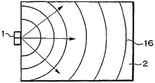
도 1은 본 발명의 면광원 시스템의 한가지 실시양태를 나타낸 것으로, 도면 중 1은 대략 점상의 1차 광원으로서의 LED 광원이며, 도광체(2)의 코너부에 배치된다. 도광체(2)는 1차 광원(1)이 배치되는 코너부가 원호형으로 절결되어 있고, 그 광 출사면(4) 및 그 반대측인 이면의 적어도 한쪽에 후술하는 지향성 광출사 기구를 갖고 있다. 도광체(2)의 광 출사면(4) 위에는 광 편향 소자(3)가 탑재되어 있다. 광 편광 소자(3)에서, 도광체(2)의 광 출사면(4)과 대면하는 입광면(14)에는 1차 광원(1)을 둘러싸도록 다수의 원호형 프리즘 열(5)이 병렬되어 형성되어 있다. 또한, 도광체(2)의 광 출사면(4)의 반대측인 이면에는 광 반사 시이트(6)가 배치되어 있다. FIG. 1 shows one embodiment of the surface light source system of the present invention, in which 1 is an LED light source as a substantially pointed primary light source, and is disposed at a corner of the
1차 광원(1)으로부터 출사된 광은, 도광체(2)의 광 입사면으로부터 도광체(2)중에 입사되고, 도광체(2) 내부에서 반사를 되풀이하면서 전파되고, 도광체(2)에 형성된 지향성 광출사 기구에 의해 광 출사면(4)으로부터 출사된다. 본 발명에 있어서는 도광체(2)의 광 출사면(4) 및 그 이면의 적어도 한쪽의 표면에, 조면으로 이루어진 지향성 광출사 기구, 또는 프리즘 열, 렌티큘러 렌즈 열, V자형 홈 등의 다수의 렌즈 열이 병렬되어 형성된 렌즈면으로 이루어진 지향성 광출사 기구를 부여하거나, 도광체(2) 중에 광 확산성 미립자를 함유시켜 지향성 광출사 기구를 부여함으로써, 광의 전파 방향과 평행하고 광 출사면(4)과 수직인 면내의 분포에 있어서 지향성이 있는 광이 광 출사면(4)으로부터 출사되는 것이다.The light emitted from the primary
이와 같이 도광체(2)의 광 출사면(4)으로부터 출사된 지향성 출사광은 광 편향 소자(3)의 입광면(14)에서 입사되고, 렌즈 열(5)에 의해 반사 또는 굴절되어, 예컨대, 도광체(2)의 광 출사면(4)의 법선 방향으로 출사된다. 본 실시양태에 있어서는, 광 편향 소자(3)의 입광면(14)에 단면이 대략 삼각 형상인 프리즘 열(5)이 형성되어 있기 때문에, 도광체(2)의 광 출사면(4)으로부터 출사된 지향성 출사광은, 프리즘 열(5)을 형성하는 한쪽 프리즘 면으로부터 입사하고, 다른쪽 프리즘 면에서 내면 반사(바람직하게는 내면 전반사)되어 목적하는 방향으로 편향되어 출광면(11)으로부터 출사된다.The directional outgoing light emitted from the
또한, 본 발명에 있어서는, 1차 광원(1)으로서 LED 광원 등의 대략 점상인 광원을 사용하기 때문에, 도광체(2)에 입사한 광은 광 출사면(4)과 동일 평면내에서 1차 광원(1)을 대략 중심으로 한 방사상으로 도광체(2) 내부에서 전파되고, 광 출사면(4)에서 출사되는 출사광도 마찬가지로 1차 광원(1)을 중심으로 하는 방사상으로 출사된다. 이러한 방사상으로 출사된 출사광을, 그 출사 방향에 상관없이 효율적으로 목적하는 방향으로 편향시키기 위해서, 본 발명에서는 광 편향 소자(3)에 형성되어 있는 프리즘 열(5)을 1차 광원(1)을 둘러싸도록 대략 원호형으로 병렬로 배치한다. 이와 같이, 1차 광원(1)을 둘러싸도록 프리즘 열(5)을 대략 원호형으로 병렬로 배치함으로써, 광 출사면(4)으로부터 방사형으로 출사되는 광의 대부분이 광 편향 소자(3)의 프리즘 열(5)에 대하여 대략 원호 형상으로 수직 방향으로 입사하기 때문에, 도광체(2)의 광 출사면(4)의 전영역에서 출사광을 효율적으로 특정한 방향으로 향하게 할 수 있어 휘도의 균일성을 향상시킬 수 있다.In addition, in this invention, since the light source which is substantially point shape, such as an LED light source, is used as the primary
광 편향 소자(3)에 형성되어 있는 대략 원호형의 프리즘 열(5)은 도광체(2) 내부를 전파하는 광의 분포에 따라서 그 원호형의 정도를 선정하여, 광 출사면(4)으로부터 방사상으로 출사되는 광의 대부분이 광 편향 소자(3)의 프리즘 열(5)에 대하여 수직 방향으로 입사되도록 하는 것이 바람직하다. 구체적으로는, LED 등의 점상 광원을 대략 중심으로 한 동심원상으로 원호의 반경이 조금씩 커지도록 병렬로 배치된 것을 들 수 있고, 프리즘 열의 반경의 범위는 면광원 시스템에서의 점상 광원의 위치와, 액정 표시 영역에 상당하는 면광원의 유효 영역과의 위치 관계나 크기에 따라 결정된다.The substantially circular arc-shaped
본 발명의 광 편향 소자(3)에 형성되는 프리즘 열(5)의 패턴은 1차 광원(1) 의 배치 방법에 따라서, 예컨대, 도 2 내지 5, 6a, 6b에 도시한 바와 같이, 적절히 설정할 수 있다. 도면 중의 화살표는 1차 광원(1)으로부터의 광이 도광체(2) 내부를 전파하는 방향을 나타낸다. 어느 예에 있어서도, 광 출사면(4)으로부터 방사상으로 출사되는 광의 대부분이 광 편향 소자(3)의 프리즘 열(5)에 대하여 대략 수직 방향으로 입사하도록 하는 패턴으로 프리즘 열(5)을 형성하는 것이 바람직하다. 도 2는 복수의 1차 광원(1)을 도광체(2)의 대각선 위치의 2개의 코너부에 설치한 경우의 개략도이며, 각각의 1차 광원(1)을 대략 중심으로 한 원호형의 프리즘 열(5)을 양쪽의 광 입사면으로부터의 거리가 같아지는 라인을 경계로 하여 대략 대칭이 되도록 형성한다. 도 3은 1차 광원(1)을 도광체(2)의 한 단면의 중앙에 설치하는 경우의 개략도이며, 1차 광원(1)으로부터의 방사상 방향으로 뻗은 직선에 대하여 프리즘 열(5)이 대략 수직으로 교차하고 1차 광원을 원호형으로 둘러싸도록 프리즘 열(5)을 형성한다. 도 4는 2개의 점상 광원을 도광체(2)의 한 단면의 중앙에 근접하여 설치한 1차 광원(1)을 이용한 경우의 개략도이며, 2개의 점상 광원간의 중심점에서 방사상 방향으로 뻗은 직선에 대하여 프리즘 열(5)이 대략 수직으로 교차하도록 1차 광원(1)을 원호형으로 둘러싸도록 프리즘 열(5)을 형성한다. 도 5는 2개의 1차 광원(1)을 도광체(2)의 대향하는 2개의 단면의 중앙에 설치하는 경우의 개략도이며, 각각의 1차 광원(1)을 대략 중심으로 한 원호형의 프리즘 열(5)을 도광체(2)의 중앙이 되는 라인을 경계로 하여 대략 대칭이 되도록 형성한다. 도 6a, 도 6b는 도광체(2) 이면의 중앙부에 형성된 오목부(7)에 공기, 수지 또는 투명 물질을 개재시켜 1차 광원(1)을 배치하는 경우의 개략도이며, 1차 광원(1)을 중심 으로 하는 원호형으로 프리즘 열(5)이 형성된다. 도광체(2)의 이면에 형성된 오목부(7)는 이면으로부터 광 출사면(4)까지 관통한 관통구일 수도 있다.The pattern of the
본 발명에 있어서, 광 편향 소자(3)에 형성된 프리즘 열(5)은 도광체(2)의 광 출사면(4)에 대면하여 광 편향 소자(3)의 입광면(14)에 형성될 수도 있고, 광 편향 소자(3)의 출광면(11)에 형성될 수도 있다. 우선, 광 편향 소자(3)의 입광면(14)에 형성된 경우에 대하여 도 7을 참조하여 설명한다. In the present invention, the
도 7에 도시한 바와 같이, 도광체(2)의 광 출사면(4)으로부터 출사된 출사광(실선 화살표)은 프리즘 열(5)의 1차 광원(1)에 가까운 쪽의 면(10)으로부터 광 편향 소자(3)에 입사하고, 1차 광원(1)에서 먼 쪽의 면(9)에서 내면 반사하여 목적하는 방향으로 편향된 후, 광 편향 소자(3)의 출광면(11)으로부터 출사한다. 이 때문에, 도광체(2)의 광 출사면(4)으로부터 출사된 출사광의 지향성을 대략 유지한 상태에서 그 출사 방향을 목적하는 방향으로 바꿀 수 있어, 광의 이용 효율이 높아짐과 동시에, 휘도가 높은 면광원 시스템을 달성할 수 있다. As shown in FIG. 7, the outgoing light (solid arrow) emitted from the
도광체(2)의 광 출사면(4)으로부터 출사된 출사광은, 출사광 분포의 피크광이 광 출사면(4)에 대하여 10 내지 50도 기울어진 방향이기 때문에, 프리즘 열(5)의 1차 광원(1)에서 먼 쪽의 면(9)과 광 편향 소자(3)의 기준 평면(8)이 이루는 각도는 40 내지 80도인 것이 바람직하고, 보다 바람직하게는 50 내지 65도, 더욱 바람직하게는 55 내지 65도이다. 이것은 1차 광원(1)에서 먼 쪽의 면(9)과 광 편향 소자(3)의 기준 평면(8)이 이루는 각도를 이 범위로 함으로써, 이러한 지향성을 갖는 도광체(2)로부터의 출사광을, 광 편향 소자(3)의 출광면(11)의 법선 방향의 근 방에 편향하여 출사할 수 있기 때문이다. 여기에서, 광 편향 소자(3)의 기준 평면(8)이란, 도 7에 도시한 바와 같이, 광 편향 소자(3)의 프리즘 열(5)이 형성된 면이 평활하다고 가정했을 때의 평면으로 한다.The outgoing light emitted from the
한편, 도광체(2) 내부를 전파하는 광의 일부는 도광체(2)의 말단까지 도달하고, 그 단면에서 반사되어 되돌아오는 광(12)이 존재한다. 이러한 광(12)은 도광체(2)의 광 입사면을 향하여 도광체(2) 내부를 전파하여, 도광체(2)에 형성된 지향성 광출사 기구에 의해 광 출사면(4)으로부터 출사(점선 화살표)된다. 이러한 출사광은, 광 편향 소자(3)의 1차 광원(1)에서 먼 쪽의 프리즘 면(9)으로부터 입사되고, 1차 광원(1)에 가까운 쪽의 프리즘 면(10)에서 내면 반사되어 목적하는 방향으로 편향된 후, 광 편향 소자(3)의 출광면(11)으로부터 출사된다. 이러한 출사광도, 출사광 분포의 피크광이 광 출사면(4)에 대하여 10 내지 50도 기울어진 방향이기 때문에, 이러한 출사광이 비교적 많은 경우에는 프리즘 열(5)의 1차 광원(1)에 가까운 쪽의 프리즘 면(10)과 광 편향 소자(3)의 기준 평면(8)이 이루는 각도도, 1차 광원(1)에서 먼 쪽의 프리즘 면(9)과 같이 40 내지 80도인 것이 바람직하고, 보다 바람직하게는 50 내지 65도, 더욱 바람직하게는 55 내지 65도이다.On the other hand, a part of the light propagating inside the
광 편향 소자(3)의 기준 평면(8)에 대한 프리즘 면(9)이 이루는 각도와 프리즘 면(10)이 이루는 각도는 동일하게 할 수도 있고, 상이하게 할 수도 있다. 양 각도를 상이하게 하는 경우에는 그 차이가 10도 이하인 것이 바람직하고, 보다 바람직하게는 5도 이하, 더욱 바람직하게는 2도 이하이다.The angle made by the prism face 9 and the angle made by the
본 발명에 있어서, 휴대 전화나 휴대용 정보 단말기 등과 같은 휴대용 전자 기기의 면광원 시스템과 같이, 소비 전력의 저감화와 고휘도화의 요구가 매우 높은 용도에서는 광 편향 소자(3)에 형성된 프리즘 열(5)의 단면 형상을, 도 8에 도시한 바와 같이 프리즘 면을 볼록형의 곡면 형상으로 함으로써, 프리즘 면에서 내면 반사할 때에 목적하는 방향으로 집중하도록 편향시킬 수 있고, 보다 지향성이 높은 집중광으로서 출사되기 때문에 소비전력당 휘도를 높일 수 있어, 저소비 전력화 및 고휘도화를 보다 높일 수 있다. In the present invention, the
이러한 프리즘 열(5)의 형상에 대해서 도 8을 참조하면서 설명한다. 우선, 프리즘 열 배열의 피치를 P로 하고, 단면이 삼각 형상인 가상 프리즘 열(I)을 설정한다. 이 가상 프리즘 열(I)의 2개의 프리즘 면(I-1), (I-2)이 이루는 각도(즉, 가상 프리즘 꼭지각)를 θ로 한다. 이 각도(θ)는 도광체(2)의 광 출사면(4)으로부터 도래하는 광의 강도 분포의 피크 출사광(경사각 α)이 가상 프리즘 열(I)에 입사하여 가상 프리즘 면(I-2)에 의해 내면 반사(바람직하게는 내면 전반사)된 뒤에, 예컨대 출광면(11)의 법선 방향으로 진행하도록 가상 프리즘 열(I)의 꼭지각(θ)이 설정되어 있다. The shape of such a
다음에, 이상과 같이 하여 형상이 설정된 가상 프리즘 열(I)의 형상을 기준으로 하여, 그 적어도 한쪽의 프리즘 면이 볼록한 곡면 형상이 되도록 실제 프리즘 열의 형상을 정한다. 구체적으로는, 다음과 같이 하여 실제 프리즘 열의 형상을 정하는 것이 바람직하다. 도광체(2)의 광 출사면(4)으로부터 출사하는 광의 출사광 분포의 피크 출사광(경사각 α)이 1차 광원(1)측의 인접 가상 프리즘 열의 꼭대기부를 스쳐서 가상 프리즘(I)에 입사하는 가상광을 설정하고, 이 가상광이 가상 프리즘 면 (I-1)을 통과하는 위치를 K1으로 하고, 가상 프리즘 면(I-2)에 도달하는 위치를 K2로 한다. 이 때, 이 프리즘 열의 형상은 가상 프리즘 열(I)에 있어서의 프리즘 면(I-2)의 내면 전반사 위치(K2)보다도 출광면(11)에 가까운 위치에서는 그 적어도 일부 또는 전부에 프리즘 면의 경사각이 가상 프리즘 열(I)의 프리즘 면(I-2)의 경사각보다도 큰 경사각을 갖도록 볼록 곡면 형상으로 하는 것이 바람직하다.Next, on the basis of the shape of the virtual prism row I in which the shape is set as described above, the shape of the actual prism row is determined so that at least one prism face becomes a convex curved shape. Specifically, it is preferable to determine the shape of the actual prism row as follows. The peak outgoing light (inclined angle α) of the outgoing light distribution of the light exiting from the
이는, 도 8에 도시되어 있는 치수(z)(프리즘 열의 정점과 가상 프리즘 면(I-2)의 내면 반사 위치(K2)간의 출광면(11)의 법선 방향의 거리)가 다음 수학식 1로 표시되는 값 이상의 출광면 법선 방향 위치에서는 실제의 프리즘 면이 다음 수학식 2로 표시되는 가상 프리즘 열(I)의 프리즘 면(I-2)보다 큰 경사각을 가지도록 하는 것이다(한편, 수학식 중 n은 프리즘 열의 굴절률이다).This means that the dimension z (the distance in the normal direction of the

![]()
![]()
이상과 같은 볼록 곡면 형상으로서는, 가상 프리즘 열과 꼭대기부 및 저부를 공통으로 하여(즉, 꼭대기부와 인접 가상 프리즘 열 사이의 골짜기부를 지나는 형상이며) 곡율 반경(r)의 볼록 원호면 형상을 예시할 수 있다. 여기에서, 피치(P)로 규격화한 곡율 반경(r)의 값(r/P)으로서는 2 내지 80의 범위로 하는 것이 바람직하고, 보다 바람직하게는 7 내지 30의 범위이다. As the above convex curved shape, the convex arc shape of the radius of curvature r is illustrated by making the virtual prism row and the top and the bottom part in common (that is, the shape passing through the valley between the top and the adjacent virtual prism rows). Can be. Here, as a value r / P of the radius of curvature r normalized by the pitch P, it is preferable to set it as the range of 2-80, More preferably, it is the range of 7-30.
프리즘 열(5)의 형상을 이와 같이 설정함으로써, 광 편향 소자(3)로부터 출사되는 광의 분포 각도(반값폭)를 작게 할 수 있다. 그 이유는 다음과 같다. 즉, 가상 프리즘 열(I)에서의 프리즘 면(I-2)의 내면 반사 위치(K2)보다 출광면(11)에 가까운 위치에 도달하는 광은, 1차 광원측의 인접 가상 프리즘 열의 꼭대기부보다 하측에서 α보다 큰 경사각으로 입사되는 광선의 집합이다. 따라서, 그 분포 피크의 방향은 α보다 큰 경사의 방향이며, 그 내면 반사광의 분포 피크의 방향은 출광면(11)의 법선 방향으로부터 내면 반사의 가상 프리즘 면을 따른 방향쪽으로 경사진 방향이 된다. 이러한 광은 출광면(11)으로부터의 출사광의 각도 분포를 넓히는 작용을 한다. 이에, 특정 방향으로 광량을 집중하여 출사시키기 위해, 가상 프리즘 열(I)에서의 프리즘 면(I-2)의 내면 반사 위치(K2)보다 출광면(11)에 가까운 위치에서의 실제 프리즘 열의 프리즘 면의 경사각을, 대응하는 가상 프리즘 면의 경사각보다 크게 함으로써, 이 영역에서 실제로 내면 반사된 광의 진행 방향을 가상 프리즘 면에서의 반사광보다도 출광면(11)의 법선 방향쪽으로 이동시키도록 수정할 수 있어, 고휘도화 및 협시야화를 도모할 수 있다.By setting the shape of the
가상 프리즘 면(I-1)에 대응하는 실제 프리즘 면도 동일한 형상(즉, 출광면(11)의 법선 방향에 관해서 가상 프리즘 면(I-2)에 대응하는 실제 프리즘 면과 대칭적인 형상)으로 하는 것이 바람직하다. The actual prism shaving corresponding to the virtual prism face I-1 has the same shape (that is, the shape symmetrical with the actual prism face corresponding to the virtual prism face I-2 with respect to the normal direction of the light exit face 11). It is preferable.
비대칭성 프리즘의 경우에는 상기 Z의 값에 관한 식을 직접 사용할 수는 없지만, 이 비대칭성 프리즘 열의 피치가 결정되어 광원에 가까운 쪽의 프리즘 면(I-1)이 경사각이 있는 값으로 설정되었다고 하면, 도광판으로부터 인접 가상 프리즘 의 꼭대기부를 스쳐 임의의 출사 피크 각도를 가지고 I-2면을 굴절통과한 광선이 상기 법선 방향을 향하여 프리즘 면(I-2)의 K2의 위치에서 내면 반사하여 편향하도록, K2 및 프리즘 면(I-2)의 경사 각도를 일의적으로 결정할 수 있다. 이에 따라, 가상 비대칭 삼각형을 상정할 수 있고, 상술한 협시야화를 위한 프리즘 설계 원리를 상술한 바와 같이 적용할 수 있다. In the case of an asymmetric prism, the equation for the value of Z cannot be directly used. However, if the pitch of the asymmetric prism row is determined and the prism face I-1 near the light source is set to a value having an inclination angle, The light beams that pass through the I-2 plane with an arbitrary exit peak angle by passing through the top of the adjacent virtual prism from the light guide plate are deflected internally at the position of K2 of the prism face I-2 toward the normal direction and deflected. The inclination angles of K2 and prism face I-2 can be uniquely determined. Accordingly, a virtual asymmetric triangle can be assumed, and the above-described prism design principle for narrow field of view can be applied as described above.
상기 예에서는, 광 편향 소자(3)의 출광면(11)의 법선 방향으로 출사시키는 경우에 대해서 설명했지만, 임의의 목적하는 각도로 피크 출사광을 출사시켜 협시야화를 달성하고 싶은 경우에는, 대칭 또는 비대칭성 프리즘에 상관없이 인접 가상 프리즘의 꼭대기부를 스쳐 임의의 출사 피크 각도를 가지고 I-1면을 굴절통과한 광선이 상기 목적하는 방향으로 향하도록 프리즘 면(I-2)의 경사 각도와 K2를 일의적으로 결정할 수가 있고, 역시 상술한 바와 같이 협시야화를 위한 설계 원리를 적용할 수 있다. In the above example, the case where light is emitted in the normal direction of the
이와 같은 협시야화에 있어서는, 도광체(2)의 광 입사면과 광 출사면(4)에 직교하는 면에서의 출사광 분포에 있어서, 광 편향 소자(3)의 출광면(11)으로부터의 출사광의 반값폭(A)이 도광체(2)의 광 출사면(4)으로부터의 출사광의 반값폭(B)의 30% 이상 100% 미만의 범위가 되는 것이 바람직하고, 더욱 바람직하게는 40 내지 90%의 범위이다. 이는 반값폭(A)을 반값폭(B)의 30% 이상으로 함으로써, 극단적인 협시야화에 의해 화상 등이 잘 보이지 않는 것을 방지할 수 있고, 100% 미만으로 함으로써 고휘도화와 협시야화를 도모할 수 있기 때문이다.In such narrow field of view, the emission light distribution on the light incident surface of the
한편, 상술한 경우와는 달리, 광시야화를 달성하고 싶은 경우(면광원으로부 터의 출사 각도 분포의 폭을 넓게 함)에는, 광 편향 소자(3)에 형성되는 프리즘 열(5)의 단면 형상에 있어서 프리즘 면을 오목형의 곡면 형상으로 함으로써, 프리즘 면에서 내면 반사할 때에 분포 각도를 넓히도록 편향시킬 수 있어, 시야 범위를 비교적 넓게 할 수 있다. 이 경우의 프리즘 열(5)의 형상 설정에 대해서는 상기 볼록형의 곡면 형상으로 하는 경우와 동일하게 하여 실시할 수 있고, 프리즘(I-2)의 K2의 점보다 도광체에 가까운 쪽의 일부 또는 전부의 프리즘 면에 있어서, 그 프리즘 경사 각도를 가상 프리즘 면의 그것보다 커지도록 설정함으로써, 상기 광시야화가 달성되며, 즉 출사광 분포를 보다 넓힐 수 있다. On the other hand, unlike in the case described above, when it is desired to achieve wide field of view (to broaden the width of the emission angle distribution from the surface light source), the cross section of the
다음에, 광 편향 소자(3)의 출광면(11)에 프리즘 열(5)이 형성된 경우에 대해서 도 9를 참조하여 설명한다.Next, a case in which the
도 9에 도시한 바와 같이, 도광체(2)의 광 출사면(4)으로부터 출사된 출사광은 광 편향 소자(3)의 입광면(14)에서 굴절하면서 입사된다. 입사한 광은 1차 광원(1)에서 먼 쪽의 프리즘 면(15)에 입사하고, 여기에서 굴절하면서 출사한다. 이와 같은 광 편향 소자(3)를 이용했을 경우에는 광을 편향시키는 작용이 비교적 약하기 때문에, 도광체(2)의 광 출사면(4)과 광 편향 소자(3) 사이에 광의 진행 방향을 제어하는 확산 시이트나 프리즘 시이트를 개재시킬 수도 있다. 또는, 광 편향 소자(3) 위에 다른 확산 시이트나 프리즘 시이트를 이용하여 출사광을 출광면(11)의 법선 방향으로 향하게 할 수 있다.As shown in FIG. 9, the outgoing light emitted from the
입사한 광을 주로 굴절하는 프리즘 면(15)과, 광 편향 소자(3)의 기준 평면(13)이 이루는 각도는 35 내지 55도로 하는 것이 바람직하다. 이 각도가 이 보 다도 작을 경우에는, 굴절에 의한 광의 편향 작용이 충분하지 않게 되는 경향이 있고, 이 보다 각도가 큰 경우에는, 부 피크가 커지는 경향이 있다. 여기에서, 광 편향 소자(3)의 기준 평면(13)이란, 도 9에 도시한 바와 같이 광 편향 소자(3)의 프리즘 열(5)이 형성된 면이 평활하다고 가정했을 때의 평면으로 한다. 이와 같이 프리즘 열(5)을 광 편향 소자(3)의 출광면(11)에 형성한 경우에도, 프리즘 열(5)을 광 편향 소자(3)의 입광면(14)에 형성한 경우와 같이, 프리즘 열(5)의 형상은 좌우 대략 대칭으로 할 수 있다. 2개의 프리즘 면과 기준 평면(13)이 이루는 각도가 다른 경우, 2개의 프리즘 면의 기준 평면(13)에 대하여 이루는 각도의 차이는 10도 이하로 하는 것이 바람직하고, 보다 바람직하게는 5도 이하, 더욱 바람직하게는 2도 이하이다. It is preferable that the angle formed between the
광 편향 소자(3)에 형성되는 프리즘 열(5)로서는, 프리즘 패턴을 형성할 때의 금형의 내구성 등을 고려하여 그 꼭대기부를 곡면화(즉, 단면 곡선화)하거나, 평탄화한 형상으로 할 수 있다. 이러한 형상을 사용함에 따라, 금형의 내구성을 향상시키고, 제품의 비용을 저감시키는 것이 가능해지지만, 이러한 꼭대기부의 가공은 광학적 특성을 손상시키지 않는 범위에서 실시하는 것이 필요하다. 또한, 본 발명에 있어서는, 광 편향 소자(3)로서는 도광체(2)로부터의 출사광을 목적하는 방향으로 편향(변각)시키는 기능을 하는 것으로, 상기와 같은 프리즘 열을 형성한 프리즘 시이트가 바람직하지만, 렌즈 시이트에 형성되는 렌즈 열로서는 목적에 따라 다양한 형상의 것을 사용할 수 있고, 예컨대, 렌티큘러 렌즈 형상, 플라이아이 렌즈 형상, 물결형 형상 등을 들 수 있다.As the
본 발명의 도광체(2)로서는, 1차 광원(1)으로부터 출사된 광을 1차 광원(1)을 대략 중심으로 하여 방사상으로 전파하여, 도광체(2)에 형성된 지향성 광출사 기구에 의해, 도광체(2)를 전파하는 광의 진행 방향에 평행하고 광 출사면(4)에 수직인 면에서, 출사광 분포의 피크광이 광 출사면(4)에 대하여 경사진 방향으로 출사하는 지향성을 가지고 출사시키는 것이면 특별히 한정되는 것은 아니다.As the
도광체(2)에 형성되는 지향성 광출사 기구로서는, 예컨대, 도광체(2)의 광 출사면(4) 및 이면 중 1개 이상의 표면에 요철 형상을 형성하거나, 도광체(2)중에 기재와 굴절률이 다른 구조를 형성함으로써, 예컨대 기재와 굴절률이 다른 광 확산성 미립자를 함유시킴으로써 지향성 광출사 기구를 형성할 수도 있다. 1차 광원(1)으로부터 도광체(2)에 입사된 광은 이러한 지향성 광출사 기구에 의해, 도광체(2) 내부를 전파하는 동안에 광 출사면(4)으로의 입사각이 변화되고, 광 출사면(4)으로의 입사각이 경계각 미만이 되었을 경우에 광 출사면(4)으로부터 출사된다.As the directional light output mechanism formed on the
도광체(2)의 표면을 요철 형상으로 함으로써 지향성 광출사 기구를 형성하는 경우로서는, 프리즘 열, 렌티큘러 렌즈 열, V자형 홈 등의 다수의 렌즈 열을 병렬로 형성한 렌즈면, 또는 조면(매트면)으로 하는 것 등을 들 수 있다. 이들 지향성 광 출사 기구는 복수의 지향성 광출사 기구를 조합하여 도광체(2)에 형성할 수도 있다. 이러한 지향성 광 출사 기구를 마련한 도광체(2)는 광 출사면(4)으로부터 출사하는 출사광의 출사광 분포에 있어서의 피크 출사광의 방향이 광 출사면(4)과 10 내지 50도의 각도이고, 출사광 분포의 반값폭이 10 내지 40도인 것이 바람직하 다. 특히, 상술한 프리즘 면을 볼록형의 곡면 형상으로 한 프리즘 시이트를 광 편향 소자(3)로 사용하는 경우에는 광 출사면(4)으로부터 출사하는 출사광의 출사광 분포의 반값폭이 10 내지 30도 각도인 것에 적합하다. 이는, 이러한 반값폭의 출사광을 평면 형상의 프리즘 면으로 이루어진 프리즘 시이트로 편향시켰을 경우에, 프리즘 시이트로부터 출사하는 출사광의 반값폭이 도광체(2)의 그것보다 넓어지는 경향이 있어, 고휘도화가 손상되는 경우가 있기 때문이다.In the case of forming the directional light output mechanism by making the surface of the
본 발명에 있어서, 지향성 광출사 기구로서의 조면이나 렌즈면은 ISO 4287/1-1984에 의한 평균 경사각(θa)이 2 내지 12도의 범위인 것이 바람직하고, 보다 바람직하게는 3 내지 10도의 범위이다. 이는, 평균 경사각(θa)이 2도 미만이면 도광체(2)의 광 출사율이 작아져 광의 출사량이 불충분해 지고, 휘도가 저하되는 경향이 있기 때문이며, 반대로 평균 경사각(θa)이 12도를 초과하면, 도광체(2)의 광 출사율이 커서 1차 광원(1) 근방에서의 출사광량이 커져, 광 출사면(4)내에서의 휘도의 균일성이 저하되는 경향이 있기 때문이다. 본 발명에 있어서, 조면이나 렌즈면의 평균 경사각(θa)은 도광체(2)의 표면내에서 균일하게 할 수도 있고, 연속적으로, 단속적으로, 또는 부분적으로 변화시킬 수도 있다. 예컨대, 광 출사면(4)내에서의 휘도의 균일성을 향상시키기 위해서는 1차 광원(1)으로부터 멀어짐에 따라 평균 경사각(θa)을 크게 하는 것이 바람직하다. 또한, 광 출사면(4)내에서 부분적으로 휘도가 저하되는 부분이 존재할 경우에는, 그 부분의 평균 경사각(θa)을 크게 하거나, 반대로 부분적으로 휘도가 높아지는 부분이 존재하는 경우에는 그 부분의 평균 경사각(θa)을 작게 하거나 함으로써, 출사광량을 부분적으로 제어하여 휘도의 균일화를 도모할 수 있다.In the present invention, it is preferable that the average inclination angle? A according to ISO 4287 / 1-1984 is in the range of 2 to 12 degrees, more preferably in the range of 3 to 10 degrees for the rough surface and the lens surface as the directional light output mechanism. This is because if the average inclination angle θa is less than 2 degrees, the light output rate of the
도광체(2)에 형성되는 조면이나 렌즈면의 평균 경사각(θa)은, IS0 4287/1-1984에 따라, 촉침식 표면 조도계를 사용하여 조면 형상을 측정하고, 측정 방향의 좌표를 x로하여, 수득된 경사 함수 f(x)부터 다음 수학식 3 및 4를 이용하여 구할 수 있다. 여기에서, L은 측정 길이이고, Δa는 평균 경사각(θa)의 정점이다. The average inclination angle θa of the rough surface and the lens surface formed on the
![]()
![]()
![]()
![]()
도광체(2)에 형성되는 지향성 광출사 기구의 구체적인 실시태양을 도 10 내지 13에 나타내었다. 도 10은 도광체(2)의 이면에 1차 광원(1)을 대략 중심으로 한 원호형 프리즘 열(16)을 형성한 것이다. 도 11은 도광체(2)의 이면에 1차 광원(1)을 대략 중심으로 한 방사형 프리즘 열(17)을 형성한 것이다. 도 12는 도광체(2)의 광 출사면(4)에 조면(18)을 형성한 것이다. 도 13은 도광체(2)를 구성하는 띠 형상의 상이한 굴절률층(20)을 도광체(2)의 이면에 1차 광원(1)을 대략 중심으로 한 방사상으로 형성한 것이다. 또한, 본 발명에 있어서, 지향성 광출사 기구는 이들 실시 형태로 나타내어진 것에 한정되는 것은 아니며, 다른 지향성 광출사 기구일 수도 있고, 지향성 광출사 기구를 형성하는 도광체(2)의 표면이 반대측 면일 수도 있다. 본 발명에 있어서는 이러한 지향성 출사 기능에 한정되지 않고, 도광체(2)의 내부에 도광체(2)를 구성하는 기재와 굴절률이 다른 광 확산성 미립자를 분산한 것, 층을 구성하는 기재와 굴절률이 다른 광 확산성 미립자를 분산한 확산층(19)을 도광체(2)의 광 출사면(4)에 형성한 것, 도광체(2)를 구성하는 기재와 굴절률이 다른 상이한 굴절률층(20)을 도광체(2)의 이면에 1차 광원(1)을 대략 중심으로 한 원호형으로 형성한 것이다.Specific embodiments of the directional light output mechanism formed in the
그 중에서도, 도 10에 도시한 바와 같은 1차 광원(1)을 대략 중심으로 한 원호형 프리즘 열(16)을 지향성 광출사 기구로서 형성한 것이, 도광체(2) 내부를 1차 광원(1)을 대략 중심으로 하는 방사상으로 전파하는 광의 방향이 대폭 변화되는 일없이 광 출사면(4)으로부터 출사되기 때문에, 광 편향 소자(3)에 의해 대부분의 광을 목적하는 방향으로 편향할 수 있어, 휘도가 높고, 휘도의 균일성이 우수한 면광원 시스템을 제공할 수 있는 점에서 바람직하다.Among them, an arc-shaped
이는, 본 발명에 있어서는 1차 광원(1)으로서 LED 광원 등의 대략 점상의 광원을 사용하기 때문에, 도광체(2)에 입사된 광은 광 출사면(4)과 대략 동일 평면내에서 1차 광원(1)을 대략 중심으로 한 방사상으로 도광체(2) 내부를 전파한다. 이러한 방사상으로 전파되는 광에 대하여, 원호형 프리즘 열(16)을 1차 광원(1)을 둘러싸도록 대략 원호형으로 병렬로 배치함으로써, 도광체(2) 내부를 방사상으로 전파하는 광의 대부분이 원호형 프리즘 열(16)에 대하여 대략 수직 방향으로 입사되기 때문에, 그 광 출사면(4)과 대략 동일 평면내에서의 전파 방향에 상관없이 효율적으로 목적하는 방향으로 출사시킬 수 있어, 이 전파 방향을 유지하기 쉬워짐과 동시에, 도광체(2)의 광 출사면(4)의 전 영역에서 출사광을 효율적으로 특정한 방향으로 향하게 할 수 있어, 휘도의 균일성을 향상시킬 수 있다.This is because, in the present invention, a light source of approximately point shape, such as an LED light source, is used as the primary
거의 원호형의 프리즘 열(16)은 도광체(2) 내부를 전파하는 광의 분포에 따라 그 원호형의 정도를 선정하고, 도광체(2) 내부를 방사상으로 전파하는 광의 대부분이 원호형 프리즘 열(16)에 대하여 수직 방향으로 입사되도록 하는 것이 바람직하다.The substantially arc-shaped
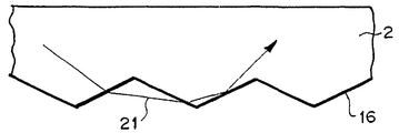
지향성 광출사 기구로서 1차 광원(1)을 중심으로 하는 원호형 프리즘 열(16)을 형성하는 경우, 형성하는 원호형 프리즘 열(16)의 지름 방향의 분포는 도 14에 도시한 바와 같이 연속하여 형성할 수도 있고, 도 15a에 도시한 바와 같이 인접하는 원호형 프리즘 열(16) 사이에 평탄부를 개재시켜 이산적으로 할 수도 있다. 원호형 프리즘 열(16)을 연속적으로 형성했을 경우, 도 14에 도시한 바와 같이 원호형 프리즘 열(16)로부터 출사된 후에, 인접하는 원호형 프리즘 열(16)에 입사된 광(21)이 존재하는 경우가 있고, 이러한 광(21)이 다량으로 존재하는 경우에는 도광체(2)로부터 출사하는 출사광의 출사광 분포의 흐트러짐이 커져, 광 편향 소자(3)에 의해 목적하는 방향으로 편향되지 않는 광이 많아짐에 따라 휘도의 저하를 초래하는 경우가 있다. 이러한 경우에는 도 15a에 도시한 바와 같이 원호형 프리즘 열(16)을 이산적으로 형성함으로서, 도 14에 도시한 21과 같은 광을 저감시킬 수 있고, 도광체(2)로부터 출사하는 출사광으로부터의 출사광 분포의 흐트러짐에 따른 휘도의 저하를 억지할 수 있다. 이와 같이, 원호형 프리즘 열(16)을 이산적으로 형성하는 경우, 원호형 프리즘 열(16)을 도 15b와 같이 오목형으로 형성할 수도 있다.In the case of forming the arc-shaped
이러한 원호형 프리즘 열(16)로서는 단면 형상이 삼각 형상, 원호형, 반원 형, 다각 형상 등의 형상인 것을 형성할 수 있다. 그 중에서도, 도 14에 도시한 바와 같은 광(21)을 저감시켜 도광체(2)로부터 출사하는 출사광으로부터의 출사광 분포의 흐트러짐에 따른 휘도의 저하를 억지할 수 있는 점에서, 단면이 대략 삼각 형상인 것이 바람직하다.As such an arc-shaped
이러한 단면이 대략 삼각 형상인 원호형 프리즘 열에 있어서는, 도 16a에 도시한 바와 같이, 그 1차 광원(1)에 가까운 쪽의 프리즘 면(23)과 도광체(2)의 기준 평면(22)이 이루는 각을 2 내지 20도로 하는 것이 바람직하고, 보다 바람직하게는 4 내지 12도의 범위이다. 이는, 도광체(2)로부터 출사하는 출사광 분포에 있어서의 피크 출사광의 출사 각도 및 출사광 분포의 반값폭이 프리즘 면(23)과 도광체(2)의 기준 평면(22)이 이루는 각에 의해 변화되기 때문이며, 프리즘 면(23)과 도광체(2)의 기준 평면(22)이 이루는 각이 20도를 초과하면, 출사광 분포의 반값폭이 커져, 휘도가 저하되는 경향이 있다. 또한, 프리즘 면(23)과 도광체(2)의 기준 평면(22)이 이루는 각이 2도 미만이면, 도광체(2)로부터의 출사 광량이 적어져 휘도가 저하되는 경향이 있다. 여기에서, 도광체(2)의 기준 평면(22)이란, 도 16a에 도시한 바와 같이 도광체(2)의 원호형 프리즘 열이 형성된 면이 평활하다고 가정했을 때의 평면으로 한다.In the arc-shaped prism array having such a triangular cross section, as shown in FIG. 16A, the
또한, 원호형 프리즘 열(16)을 이산적으로 형성했을 경우, 그 원호형 프리즘 열(16)이 형성되어 있는 프리즘부(L2)와, 인접하는 원호형 프리즘 열(16) 사이에 형성한 평탄부(L1)와의 비율 L2/L1을, 원호형 프리즘 열(16)의 둘레 방향에서 변화시킴으로써, 즉, 도광체(2)내에서의 광의 전파 방향에 있어서 광량이 많은 방향에 서는 비율 L2/L1을 작게 하고, 광량이 적은 방향에서는 비율 L2/L1을 크게 함으로써, 휘도의 균일성을 향상시킬 수 있다.In the case where the arc-shaped
또한, 이 비율 L2/L1을, 원호형 프리즘 열(16)의 지름 방향에서 변화시킴으로써, 도광체(2)의 광 출사면(4)의 코너부 등의 휘도가 낮은 영역이나, 1차 광원(1) 근방부 등의 휘도가 높은 영역에서의 휘도 불균일을 개선할 수 있다. 또한, 1차 광원(1)으로부터 멀어짐에 따라, 이 비율을 감소시킴으로써 휘도의 균제도(![]()
![]()
원호형 프리즘 열(16)은, 그 원주 방향에서도 이산적으로 형성할 수 있지만, 정확한 형상의 원호형 프리즘 열(16)을 형성하기 어렵기 때문에, 원호의 원주 방향에는 연속적으로 형성한 프리즘 열로 하는 것이 바람직하다.Although the arc-shaped
본 발명에 있어서는 도 17b와 같이, 원호형 렌즈 열(16)을 형성하는 것도 가능하다. 도 16a, 16b에서 24는 광선을 나타낸다.In the present invention, as shown in Fig. 17B, an arc-shaped
본 발명에 있어서는 도광체(2)에 원호형 프리즘 열(16) 등을 형성한 렌즈면이나 조면을, 도 17a 및 도 17b와 같이, 수지에 의해 패턴상으로 매설한 매설부(25)를 마련하여 평탄화함으로써, 휘도의 균일성을 향상시킬 수도 있다. 휘도를 높이고 싶은 부분에서는 평탄화의 비율을 작게 하고, 휘도를 억제하고 싶은 부분에서는 평탄화의 비율을 크게 하면 좋다. 이러한 패턴상 매설부(25)를 형성하기 위한 매설 수지로서는, 활성 에너지선 경화성 조성물의 중합율을 높여 증점화시킨 것 이나, 활성 에너지선 경화성 조성물에 인쇄용 잉크에 사용되는 것 같은 증점재를 혼합한 것을 사용할 수 있다.In the present invention, the buried
도광체(2)의 원호형 프리즘 열(16)의 패턴은, 1차 광원(1)의 배치 방법에 따라서, 예컨대, 도 18 내지 22에 도시한 바와 같이 적절히 설정할 수 있다. 임의의 예에 있어서도, 도광체(2) 내부를 방사상으로 전파하는 광의 대부분이 원호형 프리즘 열(16)에 대하여 수직 방향으로 입사하도록 하는 패턴으로 하고 있다. 도면 중의 화살표는 1차 광원(1)으로부터의 광이 도광체(2) 내부를 전파하는 방향을 나타낸다.The pattern of the arc-shaped
도 18은, 1차 광원(1)을 도광체(2)의 한 단면의 중앙에 설치하는 경우의 개략도이며, 1차 광원으로부터의 방사상 방향으로 뻗은 직선에 대하여, 프리즘 열이 대략 수직으로 교차하도록 1차 광원을 둘러싸도록 원호형으로 형성한다. 도 19는, 2개의 1차 광원(1)을 도광체(2)의 대각 위치가 되는 2개의 코너부에 설치하는 경우의 개략도이며, 각각의 1차 광원(1)을 대략 중심으로 한 원호형 프리즘 열(16)을 양쪽 광 입사면으로부터의 거리가 같아지는 라인을 경계로 하여 대략 대칭이 되도록 형성한다. 도 20은, 2개의 점상 광원을 도광체(2)의 한 단면의 중앙에 근접하여 설치하여 1차 광원(1)으로 사용하는 경우의 개략도로써, 두 점상 광원간의 대략 중심점으로부터 방사상으로 뻗은 직선에 대하여 프리즘 열이 대략 수직으로 교차하도록, 1차 광원(1)을 둘러싸도록 원호형으로 형성한다. 도 21은, 2개의 1차 광원(1)을 도광체(2)의 대향하는 2개의 단면의 중앙에 하나씩 설치하는 경우의 개략도로써, 각각의 1차 광원(1)을 대략 중심으로 한 원호형의 프리즘 열(16)을 도광 체(2)의 중앙이 되는 라인을 경계로 하여 대략 대칭이 되도록 형성한다. 도 22는, 도광체(2) 이면의 중앙부에 형성된 오목부에 공기, 수지 또는 투명 물질을 개재시켜 1차 광원(1)을 배치하는 경우의 개략도로써, 1차 광원(1)을 중심으로 한 원호형으로 프리즘 열(16)이 형성된다.FIG. 18 is a schematic view in the case where the primary
본 발명에 있어서는 광의 전파 방향과 수직 방향에서의 출사광 분포를 제어하거나, 특정 방향으로 광을 전파시킬 목적으로, 도 23a 내지 도 23f에 도시한 바와 같이, 1차 광원(1)을 대략 중심으로 한 방사상으로 프리즘 열 등의 요철 홈(17)을 지향성 출사 기구와 병용하여 형성할 수 있다. 도광체(2)에 지향성 출사 기구로서 조면이 형성되어 있는 경우에는, 도광체(2)에 입사한 광은 도광체(2) 내부를 전파함에 따라, 1차 광원(1)을 대략 중심으로 한 원주 방향으로 퍼져 가는 경향이 있기 때문에, 요철 홈(17)을 형성함으로써, 요철 홈(17)의 배열 방향(1차 광원(1)을 대략 중심으로 한 원주 방향)에 있어서의 출사광 분포를 좁히도록 제어할 수 있어, 휘도를 보다 높일 수 있다. 또한, 도광체(2)에 지향성 출사 기구로서 원호형 프리즘 열이 형성되어 있는 경우에는, 원호형 프리즘 열의 지름 방향의 출사광 분포가 좁아지는 경향이 있기 때문에, 요철 홈(17)을 형성함으로써, 원호형 프리즘 열의 지름 방향에 있어서의 출사광 분포를 넓히도록 제어할 수 있어 시야각을 넓게 할 수 있다. 또한, 요철 홈(17)과 평탄부의 비율을 조정함으로써 휘도의 균일성을 보다 높일 수 있다.In the present invention, as shown in Figs. 23A to 23F, for the purpose of controlling the distribution of emitted light in a direction perpendicular to the propagation direction of light or propagating light in a specific direction, the primary
방사상 요철 홈(17)의 바람직한 배열 패턴 예를 도 23a 내지 도 23f에 도시하였다. 도 23a는 방사상 요철 홈(17)의 대표예이며, 1차 광원(1)에서 멀어짐에 따라서 인접하는 요철 홈(17)의 간격이 커지도록 보통의 방사상 패턴을 도광체(2)의 광 출사면(4)에 형성한 것이다. 도 23b는 1차 광원(1)에서 멀어짐에 따라 요철 홈(17)의 깊이와 폭이 증가하는 방사상 패턴을 도광체(2)의 광 출사면(4)에 형성한 것이다. 도 23c는 길이가 비교적 짧은 다수의 요철 홈(17)을 방사상으로 배치한 패턴을 도광체(2)의 광 출사면(4)에 형성한 것이다. 도 23d는 1차 광원(1)으로부터의 광 출사 분포에 대응하여 출사 강도가 큰 방향에서는 요철 홈(17)의 깊이와 폭을 작게 하고, 출사 강도가 작은 방향에서는 요철 홈(17)의 깊이와 폭을 크게 한 것을 도광체(2)의 광 출사면(4)에 형성한 것으로, 1차 광원(1)을 대략 중심으로 한 원주 방향에 있어서의 휘도 균일성을 향상시킬 수 있다. 도 23e 및 도 23f는 휘도 불균일이 발생하기 쉬운 도광체(2)의 광 출사면(4)의 1차 광원(1)의 근방에만 요철 홈(17)을 방사상 패턴으로 형성한 것으로, 1차 광원(1) 근방의 휘도 불균일의 발생을 억지할 수 있다. 또한, 본 발명에 있어서, 방사상 요철 홈(17)은 이들 실시 형태에서 나타내어진 것에 한정되는 것은 아니며, 다른 형상, 패턴일 수도 있고, 요철 홈(17)을 형성하는 도광체(2) 표면이 반대측의 면일 수도 있다.Examples of preferred arrangement patterns of the radially
도광체(2)의 요철 홈(17)의 방사상 패턴은 광원의 배치 방법에 따라서 도 24 내지 28에 도시한 바와 같이 적절히 설정할 수 있다. 도 24는 1차 광원(1)을 도광체(2)의 한 단면의 중앙에 설치하는 경우의 개략도이며, 1차 광원(1)에서 멀어짐에 따라서 인접하는 요철 홈(17)의 간격이 커지도록 방사상 패턴을 형성한다. 도 25는 2개의 1차 광원(1)을 도광체(2)의 대각 위치가 되는 2개의 코너부에 설치하는 경우의 개략도이며, 각각의 1차 광원(1)을 대략 중심으로 한 방사상으로 요철 홈(17)을 형성하고, 도광체(2)의 중앙부에서는 양쪽의 1차 광원(1)을 대략 중심으로 한 요철 홈(17)이 서로 혼합되도록 형성한다. 도 26은 2개의 1차 광원(1)을 도광체(2)의 한 단면의 중앙에 근접하여 설치하는 경우의 개략도이며, 각각의 1차 광원(1)을 대략 중심으로 한 방사상으로 요철 홈(17)을 2개의 1차 광원(1)의 중앙을 경계로 하여 형성한다. 도 27은 2개의 1차 광원(1)을 도광체(2)의 대향하는 2개의 단면의 중앙에 하나씩 설치하는 경우의 개략도이며, 각각의 1차 광원(1)을 대략 중심으로 한 방사상으로 요철 홈(17)을 형성하고, 도광체(2)의 중앙부에서는 양쪽의 1차 광원(1)을 중심으로 한 요철 홈(17)이 서로 섞이도록 형성한다. 도 28은 도광체(2) 이면의 중앙부에 형성된 오목부에 공기, 수지 또는 투명 물질을 개재시켜 1차 광원(1)을 배치하는 경우의 개략도이며, 1차 광원(1)을 중심으로 한 방사상으로 요철 홈(17)이 형성된다. The radial pattern of the uneven |
요철 홈(17)의 형상으로서는 그 단면이 대략 삼각 형상, 원호형, 반구형, 다각 형상 등을 들 수 있다. 그 중에서도 단면이 대략 삼각 형상인 프리즘 열 또는 V 자형 홈이 효율적으로 출사광 분포를 제어할 수 있어 바람직하며, 특히 단면이 대략 이등변 삼각형인 것이 바람직하다. 이러한 단면이 대략 삼각 형상인 요철 홈(17)으로서는, 도 29에 도시한 바와 같이, 요철 홈(17)의 주면(26)과 도광체(2)의 기준 평면(22)이 이루는 각에 의해서, 도광체(2)의 광 출사면(4)으로부터 출사된 출사광의, 요철 홈(17)의 배열 방향(1차 광원(1)을 대략 중심으로 한 원주 방향)에 있어서의 출사광 분포를 제어하는 효율이 변화된다. 이 때문에 도광체(2)의 기준 평면(22)과 요철 홈(17)의 주면(26)이 이루는 각은 15 내지 65도가 바람직하 고, 보다 바람직하게는 15 내지 40도의 범위이며, 더욱 바람직하게는 20 내지 25도의 범위이다.As the shape of the
단면이 대략 삼각 형상인 요철 홈(17)은 그 꼭대기부가 평탄 또는 곡면 형상(즉 단면이 곡선 형상)일 수도 있다. 꼭대기부를 곡선형으로 하는 경우에는 꼭대기부의 곡률 반경(R)과 삼각 형상의 저변의 길이(요철 홈(17)의 폭)(P)의 비율 R/P를 0.1 내지 0.7로 하는 것이 바람직하다. R/P를 이 범위로 함으로써, 도광체(2)의 광 출사면(4)으로부터 출사하는 출사광의 요철 홈(17)의 배열 방향에 있어서의 출사광 분포를 효율적으로 제어할 수 있다. The
또한, 본 발명에 있어서, 도광체(2)의 형상으로서는 두께가 균일한 판형, 쐐기형, 배 형상 등의 다양한 형상의 것이 사용할 수 있지만, 두께가 1차 광원(1)에서 멀어짐에 따라 얇아지는 쐐기형인 것이 특히 바람직하다.In addition, in the present invention, as the shape of the
본 발명의 면광원 시스템에 사용하는 1차 광원(1)으로서는 소비 전력 등의 점에서 LED 광원이 바람직하지만, 할로겐 램프 등과 같은 다른 대략 점상의 광원을 사용할 수도 있다. 이러한 대략 점상의 1차 광원(1)은 도 1, 도 2에 도시한 바와 같이 도광체(2)의 코너부에 직선형이나 원호형의 절결을 마련하여 배치할 수도 있고, 도 3 내지 도 5와 같이, 도광체 단면에 배치할 수도 있으며, 도 6과 같이 면광원 도광체의 내부에 배치할 수도 있다. 또한, 대략 점상의 1차 광원(1)으로서는 단색광인 것, 빨강, 초록, 파랑의 3원색 파장의 광을 갖는 백색 광원 등을 사용할 수 있다. 본 발명에 있어서는, 이러한 1차 광원(1)으로서 대략 점상의 광원을 1개 또는 복수개 사용할 수 있다. 복수의 대략 점상의 광원을 사용하는 경우에는 도 2 또는 도 5와 같이 도광체(2)의 복수의 코너부 또는 단면에 1개씩 배치할 수도 있고, 도 4와 같이 하나의 코너부 또는 단면에 복수의 대략 점상의 광원을 근접하여 배치할 수도 있다. 또한, 하나의 코너부 또는 단면에 복수의 대략 점상의 광원을 근접하여 배치하는 경우에는 복수의 대략 점상의 광원을 어레이화한 LED 어레이 등을 사용할 수도 있다. As the primary
1차 광원(1)으로서는 목적이나 요구 특성에 따라서 최적의 발광 패턴(출사광 분포)의 것을 사용하는 것이 바람직하다. 일반적으로는, 1차 광원(1)의 전방(정면)의 휘도가 다른 부분보다 높아지는 현상을 완화시키기 위해서, 도광체(2)의 광 출사면(4)에 평행한 방향(a)에서의 발광 패턴의 퍼짐은 큰 것이 바람직하고, 발광패턴의 피크 반값폭이 120 내지 180도 정도인 것이 바람직하다. 1차 광원(1)을 도광체(2)의 단면 또는 코너부에 설치하는 경우의 발광 패턴의 바람직한 실시양태에 대하여, 도 30a 내지 도 30c를 참조하여 설명한다. 도 30a에 도시한 바와 같이, 도광체(2)의 단면에 1차 광원(1)을 설치하는 경우에는, a 방향의 퍼짐이 큰 발광 패턴의 것을 사용하는 것이 바람직하고, 피크 반값폭이 140 내지 180도 정도인 것이 바람직하다. 또한, 도 30b나 도 30c에 도시한 바와 같이, 도광체(2)의 코너부에 1차 광원(1)을 설치하는 경우에는, 도광체(2)중에 입사한 광이 도광체(2)의 a 방향에 있어서 전면을 향해 넓어지는 것이 바람직하고, 입사한 광의 퍼짐 각도가 도광체(2) 면의 퍼짐에 대략 일치하는 것이 바람직하다. 이 때문에, 광을 입사하는 도광체(2)의 코너의 각도가 90도인 경우에는 1차 광원(1)의 a 방향의 발광 패턴의 피크 반값폭이 60 내지 120도 정도인 것이 바람직하고, 코너의 각도가 45도인 경우에는 1차 광원(1)의 a 방향의 발광 패턴의 피크 반값폭이 20 내지 70도 정도인 것이 바람직하다. As the primary
또한, 1차 광원(1)의 광 출사면(4)에 수직인 방향(b)의 발광 패턴은 그 피크 반값폭이 10 내지 90도 정도인 것이 바람직하다. 이는 b 방향의 발광 패턴이 너무 넓으면 광은 1차 광원(1)의 근방에서 출사되기 쉬워져 휘도의 균일성이 저하되는 경향이 있고, b 방향의 발광 패턴이 너무 좁으면 도광체(2)로부터의 출사율이 작아져서 휘도가 저하되는 경향이 있기 때문이다.In addition, it is preferable that the peak half value width of the light emission pattern in the direction b perpendicular to the
도광체(2)내에서의 a 방향에서의 입사된 광의 퍼짐 각도를 크게하기 위해서는 모든 방향의 광을 반사하지 않고서 입사할 수 있도록, 1차 광원(1)을 배치하는 도광체(2)의 단면에 1차 광원(1)을 중심으로 하는 원호형의 절결부(27)를 마련하는 것이 바람직하다. 또한, 도광체(2)의 광 출사면(4)내에서의 휘도 분포를 조정할 목적으로, 절결부(27)를 비구면으로 할 수도 있다.In order to increase the spread angle of the incident light in the a direction in the
또한, 직선형으로 절결한 입광부의 면 위에 렌티큘러 렌즈 등의 렌즈 열을 형성할 수도 있다. 이 경우, 렌즈 열의 피치는 10 내지 200μm의 범위로 하는 것이 바람직하고, 보다 바람직하게는 20 내지 100μm이다. 이 피치가 너무 작으면, 입사광을 도광판 내부에서 효율적으로 퍼트리기 위한 정확한 형상 부여가 곤란해져, 목적하는 성능을 얻을 수 없게 되는 경향이 있다. 한편, 렌즈 열의 피치가 너무 크면, 절결부의 유효 에리어내에 배치할 수 있는 렌즈 열의 수가 적어져, 렌즈 열의 부분적인 형상 결함이 생겼을 경우에, 도광체(2) 내부의 광의 분포에 불균일한 휘도의 치우침이 쉽게 시인되는 경향이 있다.It is also possible to form a lens array such as a lenticular lens on the surface of the light incidence portion cut straight. In this case, the pitch of the lens rows is preferably in the range of 10 to 200 m, more preferably 20 to 100 m. If the pitch is too small, it is difficult to give an accurate shape for efficiently spreading the incident light inside the light guide plate, and thus there is a tendency that the desired performance cannot be obtained. On the other hand, if the pitch of the lens rows is too large, the number of lens rows that can be arranged in the effective area of the cutouts decreases, and when partial shape defects occur in the lens rows, the luminance uneven in the light distribution inside the
본 발명에 있어서는 1차 광원(1)으로서 비교적 지향성이 높은 LED 등의 점상 광원을 사용하기 때문에, 특히 도광체(2)의 표면에 지향성 출사 기구로서 렌즈 열을 형성한 경우에는 도광체(2)의 광 출사면(4)과 동일면내에서의 출사광 분포가 몇도 내지 십몇도로 매우 좁아지는 경우가 있고, 광 출사면(4)의 법선 방향에서 관찰했을 경우에 1차 광원(1)을 대략 중심으로 한 부채형의 휘선이 관찰될 수 있다. 이러한 경우에, 도광체(2)의 렌즈 열을 형성한 표면을 미세한 조면으로 함으로써, 도광체(2)의 광 출사면(4)과 동일 평면내에서의 출사광 분포를 넓혀, 1차 광원(1)을 대략 중심으로 한 부채형 휘선의 발생을 억제할 수 있다. 이 경우, 조면화는 렌즈 열을 형성한 면 대신에 그 반대측의 면에 실시할 수 있고, 양쪽 면에 실시할 수도 있다.In the present invention, since a point light source such as a relatively high directivity LED is used as the primary
이 조면의 정도는 렌즈면에 대한 IS0 4287/1-1984에 의한 평균 경사각(θa)을 0.1 내지 8도의 범위로 하는 것이 바람직하고, 보다 바람직하게는 0.5 내지 6도의 범위이며, 더욱 바람직하게는 1 내지 4도의 범위이다. 이 조면의 평균 경사각(θa)이 0.1도 미만이면, 광 출사면(4)과 동일 평면내에서의 출사광 분포의 확대 효과를 충분히 얻을 수 없는 경향이 있다. 또한, 조면의 평균 경사각(θa)이 8도를 초과하면, 렌즈 열의 형상 붕괴가 커져, 렌즈 열의 지향성 광출사 특성이 손상되거나, 광 입사 단면 근방에서의 출사광량이 너무 증대하여 휘도의 균제도가 손상되는 경향이 있다.The roughness is preferably in the range of 0.1 to 8 degrees, more preferably in the range of 0.5 to 6 degrees, and more preferably in the range of 0.1 to 8 degrees with respect to the lens surface by IS0 4287 / 1-1984. To 4 degrees. If the average inclination angle θa of the rough surface is less than 0.1 degree, there is a tendency that the effect of expanding the output light distribution in the same plane as the
또한, 이방 확산성의 확산 시이트를 광 편향 소자(3)의 출광면(11) 위에 탑재함으로써도 동일한 효과를 얻을 수 있다. 이 경우, 이방성 확산 시이트의 확산 성이 강한 방향이, 1차 광원(1)의 정면 방향으로 뻗은 선과 수직이 되도록 이방성 확산 시이트를 배치한다. 또한, 도광체(2)의 표면에 형성되는 렌즈 열의 높이를, 렌즈 열이 뻗은 방향에 있어서 소정 간격으로 변화시키는 것으로도 동일한 효과를 얻을 수 있다. 이 경우, 렌즈 열의 높이를 높게 하고, 렌즈 열의 높이를 바꾸는 간격을 작게 할수록 출사광 분포를 넓힐 수 있다. 렌즈 열의 높이의 변화는 1 내지 30μm의 범위로 하는 것이 바람직하고, 간격은 10 내지 1000μm의 범위로 하는 것이 바람직하다. The same effect can also be obtained by mounting an anisotropic diffusion sheet on the
도광체(2) 및 광 편향 소자(3)를 구성하는 재료로서는 유리나 합성 수지 등의 광투과성이 높은 재료를 사용할 수 있다. 합성 수지로서는, 예컨대, 아크릴계수지, 폴리카보네이트계 수지, 염화비닐계 수지, 폴리올레핀 수지, 폴리스티렌, 또는 메틸메타크릴레이트와 스티렌의 공중합체 등을 들 수 있고, 이러한 합성 수지를 압출 성형, 사출 성형 등의 통상의 성형 방법으로 판상체로 성형함으로써 도광체(2)나 광 편향 소자(3)를 제조할 수 있다. 특히, 폴리메틸메타크릴레이트 등의 메타크릴 수지가, 그 광선 투과율의 높이, 내열성, 역학적 특성, 성형 가공성도 우수하며, 도광체용 재료로서 가장 적합하다. 이러한 메타크릴 수지란, 메틸 메타크릴레이트를 주성분으로 하는 수지이며, 메틸 메타크릴레이트가 80중량%인 것이 바람직하다. As a material which comprises the
본 발명에서, 도광체(2) 및 광 편향 소자(3)에 프리즘 형상 등의 표면 형상을 부여하기 위해서는 활성 에너지선 경화성 수지 조성물을 사용할 수도 있다. 활성 에너지선 경화성 수지 조성물로서는, 분자내에 아크릴로일기 또는 메타크릴로일 기를 갖는 중합성 화합물, 활성 에너지선 감응성 라디칼 중합개시제, 활성 에너지선 흡수제 등을 주성분으로 하는 조성물이 사용된다. 분자내에 (메트)아크릴로일기를 갖는 중합성 화합물로서는, 광 중합성 올리고머, 다작용 (메트)아크릴레이트, 단일작용 (메트)아크릴레이트 등의 화합물을 들 수 있다. 광 중합성 올리고머로서는, 분자내에 2개 이상의 이소시아네이트기를 갖는 폴리이소시아네이트와 분자내에 히드록실기와 (메트)아크릴로일기를 갖는 화합물을 반응시켜 수득되는 우레탄 폴리(메트)아크릴레이트 올리고머, 분자내에 2개 이상의 에폭시기를 갖는 에폭시 화합물과 분자내에 카복실기와 (메트)아크릴로일기를 갖는 화합물을 반응시켜 수득되는 에폭시폴리(메트)아크릴레이트 올리고머 등을 들 수 있다.In this invention, in order to provide surface shape, such as a prism shape, to the
구체적으로는, 이소포론 디이소시아네이트, 테트라메틸크실릴렌 디이소시아네이트, 크실릴렌 디이소시아네이트, 톨릴렌 디이소시아네이트 등의 디이소시아네이트 화합물과 히드록시에틸(메트)아크릴레이트, 히드록시프로필(메트)아크릴레이트, 테트라메틸올메탄트리(메트)아크릴레이트, 글리세린 디(메트)아크릴레이트 등의 히드록시기 함유 (메트)아크릴레이트 화합물을 반응하여 수득되는 우레탄 폴리(메트)아크릴레이트 올리고머, 비스페놀 A 디글리시딜 에테르, 비스페놀 F 디글리시딜 에테르, 비스페놀 S 디글리시딜 에테르, 테트라브로모비스페놀 A 디글리시딜 에테르 등의 에폭시 화합물과 (메트)아크릴산과의 반응으로 수득되는 에폭시 폴리(메트)아크릴레이트 올리고머 등을 대표로 들 수 있다.Specifically, diisocyanate compounds, such as isophorone diisocyanate, tetramethyl xylylene diisocyanate, xylylene diisocyanate, tolylene diisocyanate, hydroxyethyl (meth) acrylate, and hydroxypropyl (meth) acrylate Urethane poly (meth) acrylate oligomers obtained by reacting hydroxy group-containing (meth) acrylate compounds such as tetramethylolmethanetri (meth) acrylate, glycerin di (meth) acrylate, and bisphenol A diglycidyl ether Epoxy poly (meth) acrylate oligomers obtained by reaction of epoxy compounds with (meth) acrylic acid, such as bisphenol F diglycidyl ether, bisphenol S diglycidyl ether and tetrabromobisphenol A diglycidyl ether Etc. can be mentioned as a representative.
다작용(메트)아크릴레이트 화합물로서는, 에틸렌글리콜 디(메트)아크릴레이트, 디에틸렌글리콜 디(메트)아크릴레이트, 트리에틸렌글리콜 디(메트)아크릴레이 트, 폴리에틸렌글리콜 디(메트)아크릴레이트, 트리프로필렌글리콜 디(메트)아크릴레이트, 폴리프로필렌글리콜 디(메트)아크릴레이트, 폴리부틸렌글리콜디(메트)아크릴레이트, 1,3-부틸렌글리콜 디(메트)아크릴레이트, 1,6-헥산디올 디(메트)아크릴레이트, 네오펜틸글리콜 디(메트)아크릴레이트, 2,2-비스[4-(메트)아크릴로일옥시페닐]-프로판, 2,2-비스[4-(메트)아크릴로일옥시에톡시페닐]-프로판, 2,2-비스[4-(메트)아크릴로일옥시 디에톡시페닐]-프로판, 2,2-비스[4-(메트)아크릴로일옥시펜타에톡시페닐]-프로판, 2,2-비스[4-(메트)아크릴로일옥시에톡시-3-페닐페닐]-프로판, 비스[4-(메트)아크릴로일티오페닐]설파이드, 비스[4-(메트)아크릴로일옥시페닐]-설폰, 비스[4-(메트)아크릴로일옥시에톡시페닐]-설폰, 비스[4-(메트)아크릴로일옥시디에톡시페닐]-설폰, 비스[4-(메트)아크릴로일옥시펜타에톡시페닐]-설폰, 비스[4-(메트)아크릴로일옥시에톡시-3-페닐페닐]-설폰, 비스[4-(메트)아크릴로일옥시에톡시-3,5-디메틸페닐]-설폰, 비스[4-(메트)아크릴로일옥시페닐]-설파이드, 비스[4-(메트)아크릴로일옥시에톡시페닐]-설파이드, 비스[4-(메트)아크릴로일옥시펜타에톡시페닐]-설파이드, 비스[4-(메트)아크릴로일옥시에톡시-3-페닐페닐]-설파이드, 비스[4-(메트)아크릴로일옥시에톡시-3,5-디메틸페닐]-설파이드, 2,2-비스[4-(메트)아크릴로일옥시에톡시-3,5-디브로모페닐프로판], 트리메틸올프로판트리(메트)아크릴레이트, 테트라메틸올메탄트리(메트)아크릴레이트, 테트라메틸올메탄테트라(메트)아크릴레이트, 디펜타에리트리톨헥사(메트)아크릴레이트 등을 들 수 있다. As the polyfunctional (meth) acrylate compound, ethylene glycol di (meth) acrylate, diethylene glycol di (meth) acrylate, triethylene glycol di (meth) acrylate, polyethylene glycol di (meth) acrylate, tri Propylene glycol di (meth) acrylate, polypropylene glycol di (meth) acrylate, polybutylene glycol di (meth) acrylate, 1,3-butylene glycol di (meth) acrylate, 1,6-hexanediol Di (meth) acrylate, neopentylglycol di (meth) acrylate, 2,2-bis [4- (meth) acryloyloxyphenyl] -propane, 2,2-bis [4- (meth) acrylo Yloxyethoxyphenyl] -propane, 2,2-bis [4- (meth) acryloyloxy diethoxyphenyl] -propane, 2,2-bis [4- (meth) acryloyloxypentaethoxyphenyl ] -Propane, 2,2-bis [4- (meth) acryloyloxyethoxy-3-phenylphenyl] -propane, bis [4- (meth) acryloylthio Nil] sulfide, bis [4- (meth) acryloyloxyphenyl] -sulfone, bis [4- (meth) acryloyloxyethoxyphenyl] -sulfone, bis [4- (meth) acryloyloxydie Oxyphenyl] -sulfone, bis [4- (meth) acryloyloxypentaethoxyphenyl] -sulfone, bis [4- (meth) acryloyloxyethoxy-3-phenylphenyl] -sulfone, bis [4 -(Meth) acryloyloxyethoxy-3,5-dimethylphenyl] -sulfone, bis [4- (meth) acryloyloxyphenyl] -sulfide, bis [4- (meth) acryloyloxyethoxy Phenyl] -sulfide, bis [4- (meth) acryloyloxypentaethoxyphenyl] -sulfide, bis [4- (meth) acryloyloxyethoxy-3-phenylphenyl] -sulfide, bis [4- (Meth) acryloyloxyethoxy-3,5-dimethylphenyl] -sulfide, 2,2-bis [4- (meth) acryloyloxyethoxy-3,5-dibromophenylpropane], trimethyl All propane tri (meth) acrylate, tetramethylol methane tri (meth) acrylate, tetrameth And the like methane tetra (meth) acrylate, dipentaerythritol hexa (meth) acrylate.
단일작용(메트)아크릴레이트 화합물로서는 페닐(메트)아크릴레이트, 벤질(메 트)아크릴레이트, 페닐에틸(메트)아크릴레이트, 페녹시에틸(메트)아크릴레이트, 파라큐밀페놀에틸렌 옥사이드 변성(메트)아크릴레이트, 이소보닐(메트)아크릴레이트, 시클로헥실(메트)아크릴레이트, 디시클로펜테닐(메트)아크릴레이트, 디시클로펜타닐(메트)아크릴레이트, 테트라히드로푸르푸릴(메트)아크릴레이트, 메틸(메트)아크릴레이트, 에틸(메트)아크릴레이트, 프로필(메트)아크릴레이트, n-부틸(메트)아크릴레이트, i-부틸(메트)아크릴레이트, t-부틸(메트)아크릴레이트, 펜틸(메트)아크릴레이트, 2-에틸헥실(메트)아크릴레이트, n-헥실(메트)아크릴레이트, 2-히드록시에틸(메트)아크릴레이트, 2-히드록시프로필(메트)아크릴레이트, 2-히드록시부틸(메트)아크릴레이트, 4-히드록시부틸(메트)아크릴레이트, 테트라히드로푸르푸릴(메트)아크릴레이트, 포스포에틸(메트)아크릴레이트 등을 들 수 있다. 본 발명에 있어서는, 상기와 같은 화합물을 단독으로 사용할 수 있고, 2종 이상을 혼합하여 사용할 수 있다.As the monofunctional (meth) acrylate compound, phenyl (meth) acrylate, benzyl (meth) acrylate, phenylethyl (meth) acrylate, phenoxyethyl (meth) acrylate, paracumylphenol ethylene oxide modified (meth) Acrylate, isobonyl (meth) acrylate, cyclohexyl (meth) acrylate, dicyclopentenyl (meth) acrylate, dicyclopentanyl (meth) acrylate, tetrahydrofurfuryl (meth) acrylate, methyl ( Meth) acrylate, ethyl (meth) acrylate, propyl (meth) acrylate, n-butyl (meth) acrylate, i-butyl (meth) acrylate, t-butyl (meth) acrylate, pentyl (meth) Acrylate, 2-ethylhexyl (meth) acrylate, n-hexyl (meth) acrylate, 2-hydroxyethyl (meth) acrylate, 2-hydroxypropyl (meth) acrylate, 2-hydroxybutyl ( Meth) acrylate, 4- De-hydroxybutyl (meth) acrylate, tetrahydrofurfuryl (meth) acrylate, phosphoethyl (meth) acrylate. In the present invention, the above compounds may be used alone, or two or more kinds thereof may be mixed and used.
본 발명에서 사용하는 활성 에너지선 감응성 라디칼 중합개시제는 자외선 등의 활성 에너지선에 감응하여 라디칼을 발생시켜, 상술한 중합성 화합물의 중합을 개시하게 하는 성분이다. 활성 에너지선 감응성 라디칼 중합개시제는 360 내지 400nm의 파장역에 광 흡수를 가지며, 400nm 이상의 파장역에 실질적으로 흡수를 갖지 않는 것이 바람직하다. 이는 활성 에너지선 감응성 라디칼 중합개시제가 360 내지 400nm의 파장역에 흡수를 가짐으로서 활성 에너지선 흡수제가 흡수하지 않는 활성 에너지선을 흡수하여 효율적으로 라디칼을 발생할 수 있기 때문이다. 또한, 400nm 이상의 파장역에 실질적으로 흡수가 없음에 따라, 착색이 없는 렌즈부를 형 성할 수 있기 때문이다. 또한, 400nm 이상의 파장역에 실질적으로 흡수가 없다는 것은 실제 활성 에너지선 감응성 라디칼 중합개시제의 사용 농도 및 누광 모듈레이터의 두께에 있어서, 400nm 이상의 파장역에 활성 에너지선 감응성 라디칼 중합개시제에 기인하는 흡수가 1% 이하인 것을 의미한다. 활성 에너지선 감응성 라디칼 중합개시제의 배합량은 상기 중합성 화합물 100중량부에 대하여 0.01 내지 5중량부의 범위로 하는 것이 바람직하고, 더욱 바람직하게는 0.1 내지 3중량부의 범위이다. 이것은 활성 에너지선 감응성 라디칼 중합개시제의 배합량이 0.01중량부 미만이면 활성 에너지선 조사에 의한 경화가 늦어지는 경향이 있고, 반대로 5중량부를 초과하면 수득된 렌즈부가 쉽게 착색되는 경향이 있기 때문이다.The active energy ray sensitive radical polymerization initiator used by this invention is a component which generate | occur | produces a radical in response to active energy rays, such as an ultraviolet-ray, and initiates superposition | polymerization of the polymeric compound mentioned above. It is preferable that an active energy ray sensitive radical polymerization initiator has light absorption in the wavelength range of 360-400 nm, and does not have an absorption substantially in the wavelength range of 400 nm or more. This is because the active energy ray-sensitive radical polymerization initiator has absorption in the wavelength range of 360 to 400 nm, so that the active energy ray absorbent absorbs the active energy ray not absorbed and can efficiently generate radicals. In addition, since there is substantially no absorption in the wavelength range of 400 nm or more, it is possible to form a lens part without coloring. In addition, substantially no absorption in the wavelength range of 400 nm or more means that the absorption due to the active energy ray-sensitive radical polymerization initiator in the wavelength range of 400 nm or more in terms of the actual concentration of the active energy ray-sensitive radical polymerization initiator and the thickness of the light leakage modulator is 1. It means less than%. It is preferable that the compounding quantity of an active energy ray sensitive radical polymerization initiator shall be 0.01-5 weight part with respect to 100 weight part of said polymeric compounds, More preferably, it is 0.1-3 weight part. This is because when the blending amount of the active energy ray-sensitive radical polymerization initiator is less than 0.01 part by weight, curing by the active energy ray irradiation tends to be slowed. On the contrary, when the amount exceeds 5 parts by weight, the obtained lens portion tends to be easily colored.
활성 에너지선 감응성 라디칼 중합개시제의 구체예로서는, 3,3-디메틸-4-메톡시벤조페논, 벤질디메틸케탈, p-디메틸아미노벤조산이소아밀, p-디메틸아미노벤조산에틸, 벤조페논, p-메톡시벤조페논, 2,2-디에톡시아세트페논, 2,2-디메톡시-1,2-디페닐에탄-1-온, 1-히드록시시클로헥실페닐케톤, 메틸페닐글리옥실레이트, 에틸페닐글리옥실레이트, 2-히드록시-2-메틸-1-페닐프로판-1-온, 2-메틸-1-[4-(메틸티오)페닐]-2-모르폴리노프로파논-1,2,4,6-트리메틸벤조일디페닐포스핀 옥사이드 등을 들 수 있다. 이들은 단독으로 사용할 수도 있고, 2종 이상을 혼합하여 사용할 수도 있다.Specific examples of the active energy ray-sensitive radical polymerization initiator include 3,3-dimethyl-4-methoxybenzophenone, benzyldimethyl ketal, isoamyl p-dimethylaminobenzoate, ethyl p-dimethylaminobenzoate, benzophenone and p-meth Methoxybenzophenone, 2,2-diethoxyacetphenone, 2,2-dimethoxy-1,2-diphenylethan-1-one, 1-hydroxycyclohexylphenylketone, methylphenylglyoxylate, ethylphenylglyoxyl , 2-hydroxy-2-methyl-1-phenylpropan-1-one, 2-methyl-1- [4- (methylthio) phenyl] -2-morpholinopropanone-1,2,4, 6-trimethylbenzoyldiphenylphosphine oxide, etc. are mentioned. These may be used independently, or may mix and
본 발명에 있어서는, 이들 중에서도 메틸페닐글리옥실레이트, 2-히드록시-2-메틸-1-페닐프로판-1-온, 1-히드록시시클로헥실페닐케톤, 2,2-디메톡시-1,2-디페닐에탄-1-온, 벤질디메틸케탈, 2,4,6-트리메틸벤조일디페닐포스핀 옥사이드가 경화성 면에서 특히 바람직하다.In the present invention, among these, methylphenylglyoxylate, 2-hydroxy-2-methyl-1-phenylpropan-1-one, 1-hydroxycyclohexylphenyl ketone, 2,2-dimethoxy-1,2- Diphenylethan-1-one, benzyl dimethyl ketal and 2,4,6-trimethylbenzoyldiphenylphosphine oxide are particularly preferred in view of curability.
본 발명에서 사용하는 활성 에너지선 흡수제는 외광으로서 입사해 오는 활성 에너지선을 흡수하여, 도광체층과의 활성 에너지선에 의한 열화를 억지하고, 밀착성을 장기간 확보하기 위한 성분이다. 또한, 본 발명의 활성 에너지선 경화성 조성물에는 필요에 따라, 산화방지제, 황변 방지제, 블로잉제, 안료, 침강 방지제, 소포제, 대전방지제, 흐림 방지제 등의 각종 첨가제를 함유시킬 수 있다.The active energy ray absorbent used in the present invention is a component for absorbing active energy rays incident as external light, inhibiting degradation due to active energy rays with the light guide layer, and ensuring adhesion for a long time. In addition, the active energy ray-curable composition of the present invention may contain various additives such as antioxidants, anti-yellowing agents, blowing agents, pigments, anti-settling agents, antifoaming agents, antistatic agents and antifogging agents, as necessary.
본 발명의 도광체(2) 및 광 편향 소자(3)는 상기와 같은 활성 에너지선 경화성 조성물을 이용하여 도광성 기재의 한쪽 표면 이상에 렌즈 패턴 등의 표면 형상을 형성할 수 있다. 특히, 광 편향 소자(3)는 이러한 구성의 것이 바람직하다. 도광성 기재로서는 활성 에너지선을 투과하는 것이면 특별히 한정되는 것은 아니며, 유연한 유리판 등일 수도 있지만, 일반적으로는 아크릴 수지, 폴리카보네이트 수지, 염화비닐 수지, 폴리메타크릴이미드 수지, 폴리에스테르 수지 등의 투명 합성 수지 필름, 시이트 또는 판이 사용된다. The
도광체(2)나 광 편향 소자(3)는 상기와 같은 활성 에너지선 경화성 조성물을 이용하여 표면 형상을 형성하는 방법 외에, 사출 성형, 압출 성형, 프레스 성형 등의 통상의 방법을 이용하여 제조할 수 있다. 도광체(2)의 성형 방법으로서는 사출성형이, 광 편향 소자(3)의 성형 방법으로서는 사출 성형 또는 활성 에너지선 경화성 조성물을 이용하는 방법이 특히 바람직하게 사용된다. 도광체(2)나 광 편향 소자(3)의 표면에 요철 형상을 부여하기 위해 사용되는 형으로서는 금속판 등에 절삭, 에칭, 방전 가공, 레이저 가공 등의 방법으로 프리즘 열 패턴 등의 요철 형상 등을 각인한다. 특히, 단시간에서 정확한 형상을 형성할 수 있는 절삭법이 바람직하다. 또한, 조면 형상을 갖는 형을 제작하는 경우에는 에칭부나 블라스트 등이 사용된다.The
또한, 도 16에 도시한 바와 같은, 패턴상으로 평탄화된 렌즈 열을 형성하기 위해서는 표면에 렌즈 열을 형성한 성형물에, 활성 에너지선 경화성 조성물 등을 이용하여 패턴상으로 렌즈부를 매설하도록 인쇄를 실시한 후, 활성 에너지선 등의 조사에 의해 활성 에너지선 경화성 조성물 등을 경화시킨 후, 전주에 의해서 표면 형상을 전사한 것을 도광체용 형으로 사용할 수 있다.In addition, in order to form a lens row flattened in a pattern as shown in FIG. Then, after hardening an active energy ray curable composition etc. by irradiation of an active energy ray etc., what transferred the surface shape with the electric pole can be used for the light guide type | mold.
(실시예)(Example)
이하, 실시예에 의해 본 발명을 구체적으로 설명한다.Hereinafter, an Example demonstrates this invention concretely.
평균 경사각Average tilt angle
촉침식 표면 조도계(도쿄세이키사 제조 서프 콤(SURF C0M) 570A형)로, 촉침으로써 1μmR, 55° 원추 다이아몬드침(010-2528)을 사용하여 구동 속도 0.03mm/초로 측정하였다. 추출 곡선의 평균선으로부터 경사 보정을 한 후, 상기 수학식 3 및 4에 따라 그 곡선을 미분한 곡선의 중심선 평균치를 구했다. With a stylus type surface roughness meter (SURF C0M 570A type manufactured by Tokyo Seiki Co., Ltd.), it was measured at a driving speed of 0.03 mm / sec using 1 µmR and 55 ° conical diamond needle (010-2528) as a stylus needle. After the slope correction was performed from the average line of the extraction curve, the average value of the center line of the curve obtained by differentiating the curve was calculated according to
출사광 분포의 측정Measurement of the emission light distribution
면광원 시스템의 표면에 4mmΦ의 핀 홀을 갖는 흑색 종이를 핀 홀이 표면의 중앙에 위치하도록 고정하고, 휘도계의 측정원(測定圓)이 8 내지 9mm가 되도록 거리를 조정하여, 광원을 중심으로 하는 원호의 지름 방향과 원호의 둘레 방향에서 핀 홀을 중심으로 고니오 회전축이 회전하도록 조절하였다. 각각의 방향에서 회전축을 + 80도 내지 -80도까지 0.5도 간격으로 회전시키면서 휘도계로 출사광의 휘도 분포를 측정했다. The black paper having a pinhole of 4 mm Φ on the surface of the surface light source system is fixed so that the pinhole is located at the center of the surface, and the distance is adjusted so that the measuring source of the luminance meter is 8 to 9 mm, and the center of the light source is In the radial direction of the circular arc and the circumferential direction of the circular arc, the Gonio rotation axis was adjusted around the pin hole. The luminance distribution of the emitted light was measured with a luminance meter while rotating the rotation axis in the direction of 0.5 degrees from +80 to -80 degrees in each direction.
[실시예 1]Example 1
도광체의 제작Fabrication of the light guide
경면 마무리를 한 48mm×34mm, 두께 3mm의 놋쇠판 표면에, 피치 30μm이고, 단면 형상이 꼭지각 160도의 이등변 삼각형이고, 48mm×34mm의 사각 형상의 하나의 코너 근방을 중심으로 하여 원호형 프리즘 열을 동심원상으로 형성하고, 인접하는 원호형 프리즘 열 사이에 30 내지 200μm의 평탄부를 중심부로부터 서서히 간격이 좁아지도록 형성한 원호형 프리즘 패턴을 40mm×30mm의 유효 영역(Z)에 절삭가공한 금형을 수득하였다. 수득된 금형과, 경면 마무리를 한 48mm×34mm, 두께 3mm의 놋쇠판을 이용하여 사출 성형을 하고, 장변 48mm, 단변 34mm, 두께 0.8mm의 구형의 도광판을 얻었다. 사출 성형의 재료로서는 폴리메틸 메타크릴레이트를 이용하였다.On the surface of a brass plate with a mirror finish of 48 mm x 34 mm and a thickness of 3 mm, a circular 30-m pitch, an isosceles triangle with a vertex angle of 160 degrees, and an arc-shaped prism row around a corner of a rectangular shape of 48 mm x 34 mm Obtaining a mold in which an arc-shaped prism pattern formed in a concentric shape and having a flat portion of 30 to 200 μm between the adjacent arc-shaped prism rows is gradually narrowed from the center portion in the effective area Z of 40 mm x 30 mm. It was. Injection molding was carried out using the obtained mold and a brass plate of 48 mm x 34 mm with a mirror finish and a thickness of 3 mm to obtain a spherical light guide plate having a long side of 48 mm, a short side of 34 mm and a thickness of 0.8 mm. Polymethyl methacrylate was used as a material for injection molding.
수득된 도광체는 한쪽 면이 평활면이고, 다른쪽 면에 도 31에 도시한 바와 같은 원호형 프리즘 패턴이 형성되어 있었다. 이 도광체의 원호형 프리즘 열의 중심이 되는 코너부를 단면길이 4mm의 평면상으로 절결부를 형성했다. One side of the obtained light guide was a smooth surface, and an arc-shaped prism pattern as shown in Fig. 31 was formed on the other surface. The corner part used as the center of the arc-shaped prism row of this light guide was formed in the plane of 4 mm in cross section length.
광 편향 소자의 제작Fabrication of Optical Deflection Device
경면 마무리를 한 48mm×34mm, 두께 3mm의 놋쇠판 표면에, 피치 50μm이고, 단면 형상이 65.4도의 꼭지각을 끼운 두 경사면이 곡률 반경 400μm의 볼록형 곡면 인 대략 이등변 삼각형이고, 48mm×34mm의 사각 형상의 하나의 코너 근방을 중심으로 하는 원호형 프리즘 열을 동심원상으로 병렬로 연속 설치한 원호형 프리즘 패턴을 절삭가공한 금형을 얻었다. 수득된 금형에 아크릴계 자외선 경화성 조성물을 주입하고, 188μm의 폴리에스테르 필름(도요보사 제조 A4000, 굴절률 1.600)을 포갠 뒤, 고압 수은 램프를 이용하여 폴리에스테르 필름을 통해서 자외선을 조사하여 아크릴계 자외선 경화성 조성물을 경화하여, 금형으로부터 박리하여 프리즘 시이트를 얻었다. 수득된 프리즘 시이트는 폴리에스테르 필름의 한 면에, 굴절률 1.528의 자외선 경화 수지로 이루어지고, 피치 50μm이고, 65.4도의 꼭지각을 끼운 2개의 프리즘 면이 곡률 반경 400μm의 오목형 곡면인 대략 이등변 삼각형이고, 하나의 코너 근방을 중심으로 하는 동심원상의 원호형 프리즘 열이 병렬로 연속 설치된 원호형 프리즘 패턴이 형성되어 있었다. On the surface of the brass plate with a mirror finish of 48 mm × 34 mm and thickness of 3 mm, two inclined surfaces with a pitch of 50 μm and a cross-sectional shape with a vertex angle of 65.4 degrees are approximately isosceles triangles of convex surface with a radius of 400 μm of curvature, and a square shape of 48 mm × 34 mm A mold was obtained by cutting an arc-shaped prism pattern in which arc-shaped prism rows centered around one corner were continuously installed in concentric circles in parallel. An acrylic ultraviolet curable composition was injected into the obtained mold, a 188 μm polyester film (A 4000 manufactured by Toyobo, refractive index 1.600) was stacked, and ultraviolet light was irradiated through a polyester film using a high pressure mercury lamp to obtain an acrylic ultraviolet curable composition. It hardened | cured and peeled from the metal mold | die and the prism sheet was obtained. The obtained prism sheet is a substantially isosceles triangle in which one surface of the polyester film is composed of an ultraviolet curable resin having a refractive index of 1.528, a pitch of 50 µm, and two prism surfaces having a vertex angle of 65.4 degrees are concave curved surfaces having a radius of curvature of 400 µm, An arc-shaped prism pattern was formed in which a series of concentric circular arc-shaped prisms were arranged in parallel in the center of one corner.
면광원 시스템의 제작Fabrication of surface light source system
수득된 도광체의 원호형 프리즘 패턴이 형성된 면측에 광확산 반사 필름(쓰지모토덴키 세이사쿠쇼사 제조 SU-119)을 설치하고, 도광체의 광 출사면이 되는 평활면측에, 수득된 프리즘 시이트를 원호형 프리즘 패턴을 형성한 면이 도광체측이 되고, 형성한 원호형 프리즘 열의 중심이 되는 코너부가 도광체의 절결부와 겹치도록 설치하였다. 또한, 도광체의 절결부에는 도광체의 광 출사면과 평행 방향의 피크 반값폭이 115도(±57.5도), 수직 방향의 피크 반값폭 110도(±55도)인 LED 광원을 1개 설치하여 15 mA의 전류를 흘렸다. A light-diffusion reflective film (SU-119, manufactured by Tsujimoto Denki Seisakusho Co., Ltd.) was installed on the surface side on which the arc-shaped prism pattern of the obtained light guide was formed, and the obtained prism sheet was placed on the smooth surface side serving as the light exit surface of the light guide. The surface on which the arc-shaped prism pattern was formed became the light guide side, and the corner portions serving as the centers of the arc-shaped prism rows formed overlapped the cutout portions of the light guide. In addition, at the cutout of the light guide, one LED light source having a peak half value width of 115 degrees (± 57.5 degrees) in parallel with the light exit surface of the light guide body and a peak half value width of 110 degrees (± 55 degrees) in the vertical direction is provided. Flowed 15 mA.
평가evaluation
수득된 면광원 시스템의 출사광 분포를 측정한 결과, 반값폭(피크 출사광의 휘도에 대하여 휘도치가 1/2이 되는 분포의 퍼짐각)은 광원을 중심으로 하는 원호형 프리즘 패턴의 지름 방향에서 20도, 둘레 방향에서 10도였다. 또한, 피크 출사광의 휘도는 3000cd/cm2로, 매우 휘도가 높은 것이었다. 또한, 면광원 시스템의 외관은 휘도 불균일 등의 발현도 없이 양호했다.As a result of measuring the outgoing light distribution of the obtained surface light source system, the half value width (the spreading angle of the distribution in which the brightness value is 1/2 with respect to the brightness of the peak outgoing light) was 20 in the radial direction of the arc-shaped prism pattern centered on the light source. 10 degrees in the circumferential direction. In addition, the luminance of peak exit light was 3000 cd / cm 2 , which was very high. In addition, the appearance of the surface light source system was good without the appearance of luminance unevenness.
[실시예 2]Example 2
경면 마무리를 한 48mm×34mm, 두께 3mm의 SUS판의 표면을, 입경 53μm 이하의 유리 비이드(후지세이사쿠쇼 제조 FGB-400)를 이용하여 SUS판으로부터 분사 노즐까지의 거리를 40cm로 하고, 분사 압력 1.0kgf/cm2에서 40mm×30mm의 유효 영역(Z)에 블라스트 처리를 하여 조면 가공한 금형을 수득하였다. 수득된 조면 금형과 실시예 1에서 사용한 원호형 프리즘 패턴을 형성한 금형을 이용하여 사출 성형을 하여 장변 48mm, 단변 34mm, 두께 0.8mm의 직사각형의 도광판을 얻었다. 사출 성형의 재료로서는 폴리메틸메타크릴레이트를 사용하였다.Using a glass bead (FGB-400 manufactured by Fuji Seisakusho Co., Ltd.) having a particle diameter of 53 μm or less, the surface of the SUS plate having a mirror surface finish of 48 mm x 34 mm and a thickness of 3 mm is 40 cm. Blast treatment was performed on the effective area Z of 40 mm x 30 mm at the injection pressure of 1.0 kgf / cm <2> , and the roughening process metal mold | die was obtained. Injection molding was performed using the obtained roughening mold and the mold having the arc-shaped prism pattern used in Example 1 to obtain a rectangular light guide plate having a long side of 48 mm, a short side of 34 mm, and a thickness of 0.8 mm. Polymethyl methacrylate was used as a material for injection molding.
수득된 도광체는 한쪽 면이 평균 경사각 0.6도의 조면이고, 다른쪽 면에 원호형 프리즘 패턴이 형성되어 있었다. 이 도광체의 원호형 프리즘 열의 중심이 되는 코너부를 단면 길이 4mm인 평면상으로 절결부를 형성하였다. 이어서, 피치 100μm의 오목형 렌티큘러 렌즈 열을 병렬로 연속 설치한 놋쇠판(평균 경사각 3.5도)을 가열한 상태에서 절결면에 압착하고, 도광체의 두께 방향으로 연장되는 렌티큘러 렌즈 열이 연속 설치된 렌즈면을 형성하였다.One side of the obtained light guide was a rough surface having an average inclination angle of 0.6 degrees, and an arc-shaped prism pattern was formed on the other side. The notch part which formed the corner part used as the center of the arc shape prism row of this light guide body in cross section length of 4 mm was formed. Subsequently, the lens was continuously provided with a concave lenticular lens array having a pitch of 100 µm in parallel and heated in a notch while heating a brass plate (average inclination angle of 3.5 degrees), and the lens was continuously provided with a lenticular lens array extending in the thickness direction of the light guide. A cotton was formed.
수득된 도광체와, 프리즘 면을 평면으로 한 이외에는 실시예 1과 동일하게 하여 원호형 프리즘 패턴이 형성된 광 편향 소자를 이용하여 실시예 1과 동일하게 하여 면광원 시스템을 제작했다. 이 면광원 시스템의 출사광 분포를 측정한 결과, 반값폭은 광원을 중심으로 하는 원호형 프리즘 패턴의 지름 방향에서 22도, 둘레 방향에서 27도였다. 또한, 피크 출사광의 휘도는 1600cd/cm2로, 휘도가 높았다. 또한, 면광원 시스템의 외관은 휘도 불균일 등의 발현도 없이 양호하였다.A surface light source system was fabricated in the same manner as in Example 1 except that the obtained light guide and the prism face were made flat, in the same manner as in Example 1, using an optical deflection element in which an arc-shaped prism pattern was formed. As a result of measuring the emitted light distribution of this surface light source system, the half value width was 22 degrees in the radial direction and 27 degrees in the circumferential direction of the arc-shaped prism pattern centered on the light source. In addition, the luminance of the peak output light was 1600 cd / cm 2 , and the luminance was high. In addition, the appearance of the surface light source system was good without the appearance of luminance unevenness.
[실시예 3]Example 3
경면 마무리를 한 48mm×34mm, 두께 3mm의 놋쇠판 표면에, 단면 형상이 꼭지각 130도의 이등변 삼각형이고, 48mm×34mm의 사각 형상의 하나의 코너 근방을 중심으로 하여 방사상으로 연장되는 프리즘 열을 30도 피치로, 40mm×30mm의 유효 영역(Z)의 외측에 절삭 가공에 의해 형성한 금형을 얻었다. 수득된 방사상 프리즘 패턴을 형성한 금형과 실시예 1에서 사용한 원호형 프리즘 패턴을 형성한 금형을 이용하여, 방사상 프리즘 패턴의 중심과 원호형 프리즘 패턴의 중심이 일치하도록 하여 사출 성형하여, 장변 48mm, 단변 34mm, 두께 0.8mm의 직사각형 도광판을 얻었다. 사출 성형의 재료로서는 폴리메틸메타크릴레이트를 사용하였다.On the surface of 48mm × 34mm, 3mm thick brass plate with mirror finish, the cross-sectional shape is an isosceles triangle with a vertex angle of 130 degrees, and the prism rows extending radially about 30 degrees around one corner of the square shape of 48mm × 34mm By the pitch, the metal mold | die formed by the cutting process was obtained outside the effective area Z of 40 mm x 30 mm. Using the obtained metal mold | die which formed the radial prism pattern and the metal mold | die which formed the arc-shaped prism pattern used in Example 1, injection molding was carried out so that the center of a radial prism pattern might match the center of an arc-shaped prism pattern, and it was 48 mm long. A rectangular light guide plate having a short side of 34 mm and a thickness of 0.8 mm was obtained. Polymethyl methacrylate was used as a material for injection molding.
수득된 도광체의 한쪽 면에 도 23f에 도시한 바와 같은 방사상 프리즘 패턴이 형성되었고, 다른쪽 면에 원호형 프리즘 패턴이 형성되어 있었다. 이 도광체의 원호형 프리즘 열의 중심이 되는 코너부를 단면 길이 4mm인 평면상으로 절결부를 형성하였다.A radial prism pattern as shown in Fig. 23F was formed on one surface of the obtained light guide member, and an arc-shaped prism pattern was formed on the other surface. The notch part which formed the corner part used as the center of the arc shape prism row of this light guide body in cross section length of 4 mm was formed.
수득된 도광체와, 실시예 1과 동일하게 하여 원호형 프리즘 패턴이 형성된 광 편향 소자를 이용하여, 실시예 1과 동일하게 하여 면광원 시스템을 제작했다. 이 면광원 시스템의 출사광 분포를 측정한 결과, 반값폭은 광원을 중심으로 하는 원호형 프리즘 패턴의 지름 방향에서 20도, 둘레 방향에서 18도였다. 또한, 피크 출사광의 휘도는 2000cd/cm2로, 충분히 휘도가 높았다. 또한, 면광원 시스템의 외관은 휘도 불균일 등의 발현도 없고 양호했다. The surface light source system was produced like Example 1 using the obtained light guide body and the optical deflection element in which the arc-shaped prism pattern was formed similarly to Example 1. As a result of measuring the light distribution of the surface light source system, the half width was 20 degrees in the radial direction and 18 degrees in the circumferential direction of the arc-shaped prism pattern centered on the light source. In addition, the luminance of the peak output light was 2000 cd / cm 2 , which was sufficiently high. In addition, the appearance of the surface light source system was satisfactory without expression of luminance unevenness.
[비교예 1]Comparative Example 1
경면 마무리를 한 48mm×34mm, 두께 3mm의 놋쇠판 표면에, 피치 50μm이고, 단면 형상이 63도의 꼭지각을 끼운 두 경사면이 곡률 반경 400μm의 볼록형 곡면인 대략 이등변 삼각형이고, 48mm×34mm의 사각 형상의 한쪽 대각선에 직교하는 선형 프리즘 열을 병렬로 연속 설치한 프리즘 패턴을 절삭가공한 금형을 얻었다. 수득된 금형에 아크릴계 자외선 경화성 조성물을 주입하고, 188μm의 폴리에스테르 필름(도요보사 제조 A4000, 굴절률 1.600)을 겹친 후, 고압 수은 램프를 이용하여 폴리에스테르 필름을 통해서 자외선을 조사하여 아크릴계 자외선 경화성 조성물을 경화하고, 금형으로부터 박리하여 프리즘 시이트를 얻었다. 수득된 프리즘 시이트는 폴리에스테르 필름의 한쪽 면에, 굴절률이 1.528인 자외선 경화 수지로 이루어지고, 피치 50μm이고, 63도의 꼭지각을 끼운 2개의 프리즘 면이 곡률 반경 400μm의 볼록형 곡면인 대략 이등변 삼각형의 선형 프리즘 열이 병렬로 연속 설치된 도 32에 도시한 바와 같은 프리즘 패턴이 형성되어 있었다.On the surface of the brass plate of 48 mm x 34 mm and 3 mm thickness with mirror finish, the two inclined surfaces with pitch of 50 μm and the cross-sectional shape of 63 degrees of vertex are approximately isosceles triangles of convex curved surface with 400 μm radius of curvature and rectangular shape of 48 mm x 34 mm The die which cut the prism pattern which installed the linear prism row orthogonal to one diagonal line continuously in parallel was obtained. After injecting the acrylic ultraviolet curable composition into the obtained mold, and laminating a 188 μm polyester film (Toyobo Co., Ltd. A4000, refractive index of 1.600), ultraviolet light was irradiated through a polyester film using a high pressure mercury lamp to obtain an acrylic ultraviolet curable composition. It hardened | cured and peeled from the metal mold | die and the prism sheet was obtained. The obtained prism sheet was formed of an ultraviolet curable resin having a refractive index of 1.528 on one side of a polyester film, and a substantially isosceles triangle linear shape having two prism faces with a pitch of 50 μm and a vertex angle of 63 degrees being a convex curved surface having a radius of curvature of 400 μm. A prism pattern as shown in FIG. 32 in which prism rows were arranged in parallel was formed.
수득된 광 편향 소자를 실시예 1에서 사용한 도광체에 광 편향 소자의 선형 프리즘 열이 도광체에 형성된 원호형 프리즘 패턴의 중심을 포함하는 대각선과 직교하도록 배치하는 이외에는 실시예 1과 동일하게 하여 면광원 시스템을 제작하였다. 이 면광원 시스템의 출사광 분포를 측정한 결과, 반값폭은 광원을 중심으로 하는 원호형 프리즘 패턴의 지름 방향에서 20도, 둘레 방향에서 10도였다. 또한, 피크 출사광의 휘도는 3000cd/cm2로 매우 휘도가 높았지만, 면광원 시스템의 외관은 광원을 포함한 대각선 방향만이 매우 밝고, 주변부가 어둡게 되어 휘도 불균일이 두드러졌다.The obtained optical deflecting element was arranged in the same manner as in Example 1 except that the linear prism rows of the optical deflecting element were orthogonal to the diagonal including the center of the arc-shaped prism pattern formed in the light guide. A light source system was fabricated. As a result of measuring the emitted light distribution of this surface light source system, the half value width was 20 degrees in the radial direction and 10 degrees in the circumferential direction of the arc-shaped prism pattern centered on the light source. In addition, although the luminance of the peak output light was very high at 3000 cd / cm 2 , the appearance of the surface light source system was very bright only in the diagonal direction including the light source, and the peripheral portion became dark, resulting in uneven luminance.
본 발명은 광 편향 소자로서, 적어도 한쪽 면에 다수의 프리즘 열이 1차 광원을 둘러싸도록 대략 원호형으로 병렬로 배치되어 있는 것을 사용함으로써, 저소비 전력이고 소형이며, 휘도가 높고, 휘도의 균일성이 우수한 LED 광원 등의 대략 점상의 광원을 이용한 면광원 시스템을 제공할 수 있는 것이다.The present invention uses a light deflecting element in which a plurality of prism rows are arranged substantially in parallel so as to surround a primary light source on at least one surface, so that the power consumption is small, the size is small, the luminance is high, and the luminance is uniform. It is possible to provide a surface light source system using an approximately point light source such as this excellent LED light source.
도 1은 본 발명의 면광원 시스템의 기본 구조를 나타내는 개략도이다.1 is a schematic view showing the basic structure of the surface light source system of the present invention.
도 2는 본 발명의 광 편향 소자의 프리즘 열 패턴의 한가지 실시양태를 나타내는 개략도이다. 2 is a schematic view showing one embodiment of a prism thermal pattern of the optical deflecting element of the present invention.
도 3은 본 발명의 광 편향 소자의 프리즘 열 패턴의 한가지 실시양태를 나타내는 개략도이다. 3 is a schematic diagram showing one embodiment of a prism thermal pattern of the optical deflecting element of the present invention.
도 4는 본 발명의 광 편향 소자의 프리즘 열 패턴의 한가지 실시양태를 나타내는 개략도이다. 4 is a schematic diagram showing one embodiment of a prism thermal pattern of the optical deflecting element of the present invention.
도 5는 본 발명의 광 편향 소자의 프리즘 열 패턴의 한가지 실시양태를 나타내는 개략도이다. 5 is a schematic diagram showing one embodiment of a prism thermal pattern of the optical deflecting element of the present invention.
도 6a는 본 발명의 광 편향 소자의 프리즘 열 패턴의 한가지 실시양태를 나타내는 개략적인 평면도이다. 6A is a schematic plan view showing one embodiment of a prism thermal pattern of the optical deflecting element of the present invention.
도 6b는 도 6a의 개략적인 단면도이다. 6B is a schematic cross-sectional view of FIG. 6A.
도 7은 본 발명의 광 편향 소자의 한가지 실시양태의 프리즘 단위의 형상을 나타내는 개략도이다. 7 is a schematic view showing the shape of the prism unit of one embodiment of the optical deflecting element of the present invention.
도 8은 본 발명의 광 편향 소자의 한가지 실시양태의 프리즘 단위의 형상을 나타내는 개략도이다. 8 is a schematic view showing the shape of the prism unit of one embodiment of the optical deflecting element of the present invention.
도 9는 본 발명의 광 편향 소자의 한가지 실시양태의 프리즘 단위의 형상을 나타내는 개략도이다. 9 is a schematic view showing the shape of the prism unit of one embodiment of the optical deflecting element of the present invention.
도 10은 본 발명의 도광체의 한가지 실시양태의 표면 형상을 나타내는 개략 도이다. 10 is a schematic view showing the surface shape of one embodiment of the light guide of the present invention.
도 11은 본 발명의 도광체의 한가지 실시양태의 표면 형상을 나타내는 개략도이다. 11 is a schematic view showing the surface shape of one embodiment of the light guide of the present invention.
도 12는 본 발명의 도광체의 한가지 실시양태의 표면 형상을 나타내는 개략도이다. 12 is a schematic view showing the surface shape of one embodiment of the light guide of the present invention.
도 13은 본 발명의 도광체의 한가지 실시양태의 표면 형상을 나타내는 개략도이다. Figure 13 is a schematic diagram showing the surface shape of one embodiment of the light guide of the present invention.
도 14는 표면에 원호형 프리즘 열을 형성한 본 발명의 도광체의 지름 방향의 단면을 나타내는 개략도이다. It is a schematic diagram which shows the radial cross section of the light guide of this invention in which the arc-shaped prism row was formed in the surface.
도 15a는 표면에 원호형 프리즘 열을 형성한 본 발명의 도광체의 지름 방향의 단면을 나타내는 개략도이다. It is a schematic diagram which shows the radial cross section of the light guide of this invention in which the arc-shaped prism row was formed in the surface.
도 15b는 표면에 원호형 프리즘 열을 형성한 본 발명의 도광체의 지름 방향의 단면을 나타내는 개략도이다. It is a schematic diagram which shows the radial cross section of the light guide of this invention in which the arc-shaped prism row was formed in the surface.
도 16a는 표면에 원호형 프리즘 열을 형성한 본 발명의 도광체의 지름 방향의 단면을 나타내는 개략도이다. It is a schematic diagram which shows the radial cross section of the light guide of this invention in which the arc-shaped prism row was formed in the surface.
도 16b는 표면에 원호형 렌즈 열을 형성한 본 발명의 도광체의 지름 방향의 단면을 나타내는 개략도이다. Fig. 16B is a schematic diagram showing a cross section in the radial direction of the light guide of the present invention in which an arc-shaped lens row is formed on a surface thereof.
도 17a는 표면에 원호형 프리즘 열을 형성한 본 발명의 도광체의 패턴화를 나타내는 개략 사시도이다. Fig. 17A is a schematic perspective view showing the patterning of the light guide of the present invention in which an arc-shaped prism row is formed on a surface thereof.
도 17b는 도 17a의 개략적인 단면도이다. 17B is a schematic cross-sectional view of FIG. 17A.
도 18은 본 발명의 도광체의 원호형의 프리즘 열 패턴의 한가지 실시양태를 나타내는 개략도이다. 18 is a schematic diagram showing one embodiment of the arc-shaped prismatic thermal pattern of the light guide of the present invention.
도 19는 본 발명의 도광체의 원호형의 프리즘 열 패턴의 한가지 실시양태를 나타내는 개략도이다. Fig. 19 is a schematic diagram showing one embodiment of an arc-shaped prism thermal pattern of the light guide of the present invention.
도 20은 본 발명의 도광체의 원호형의 프리즘 열 패턴의 한가지 실시양태를 나타내는 개략도이다. 20 is a schematic diagram showing one embodiment of the arc-shaped prismatic thermal pattern of the light guide of the present invention.
도 21은 본 발명의 도광체의 원호형의 프리즘 열 패턴의 한가지 실시양태를 나타내는 개략도이다. Fig. 21 is a schematic diagram showing one embodiment of the arc-shaped prismatic thermal pattern of the light guide of the present invention.
도 22는 본 발명의 도광체의 원호형의 프리즘 열 패턴의 한가지 실시양태를 나타내는 개략도이다. Fig. 22 is a schematic diagram showing one embodiment of an arc-shaped prism column pattern of the light guide of the present invention.
도 23a는 표면에 방사형 프리즘 열을 형성한 본 발명의 도광체의 프리즘 열 패턴의 한가지 실시양태를 나타내는 개략도이다. FIG. 23A is a schematic diagram illustrating one embodiment of a prism thermal pattern of a light guide of the present invention with radial prism rows formed on its surface. FIG.
도 23b는 표면에 방사형 프리즘 열을 형성한 본 발명의 도광체의 프리즘 열 패턴의 한가지 실시양태를 나타내는 개략도이다. FIG. 23B is a schematic diagram illustrating one embodiment of a prism thermal pattern of a light guide of the present invention with radial prism rows formed on its surface.
도 23c는 표면에 방사형 프리즘 열을 형성한 본 발명의 도광체의 프리즘 열 패턴의 한가지 실시양태를 나타내는 개략도이다. FIG. 23C is a schematic diagram illustrating one embodiment of a prism thermal pattern of a light guide of the present invention with radial prism rows formed on its surface. FIG.
도 23d는 표면에 방사형 프리즘 열을 형성한 본 발명의 도광체의 프리즘 열 패턴의 한가지 실시양태를 나타내는 개략도이다. FIG. 23D is a schematic diagram illustrating one embodiment of a prismatic thermal pattern of a light guide of the present invention with radial prism rows formed on its surface. FIG.
도 23e는 표면에 방사형 프리즘 열을 형성한 본 발명의 도광체의 프리즘 열 패턴의 한가지 실시양태를 나타내는 개략도이다. FIG. 23E is a schematic diagram illustrating one embodiment of a prism thermal pattern of a light guide of the present invention with radial prism rows formed on its surface.
도 23f는 표면에 방사형 프리즘 열을 형성한 본 발명의 도광체의 프리즘 열 패턴의 한가지 실시양태를 나타내는 개략도이다. FIG. 23F is a schematic diagram illustrating one embodiment of a prism thermal pattern of a light guide of the present invention in which radial prism rows are formed on a surface. FIG.
도 24는 본 발명의 도광체의 방사형 프리즘 열 패턴의 한가지 실시양태를 나타내는 개략도이다. 24 is a schematic diagram illustrating one embodiment of a radial prism thermal pattern of a light guide of the present invention.
도 25는 본 발명의 도광체의 방사형 프리즘 열 패턴의 한가지 실시양태를 나타내는 개략도이다. 25 is a schematic diagram illustrating one embodiment of a radial prism thermal pattern of a light guide of the present invention.
도 26은 본 발명의 도광체의 방사형 프리즘 열 패턴의 한가지 실시양태를 나타내는 개략도이다. Figure 26 is a schematic diagram illustrating one embodiment of a radial prism thermal pattern of a light guide of the present invention.
도 27은 본 발명의 도광체의 방사형 프리즘 열 패턴의 한가지 실시양태를 나타내는 개략도이다. Figure 27 is a schematic diagram illustrating one embodiment of a radial prism thermal pattern of a light guide of the present invention.
도 28은 본 발명의 도광체의 방사형 프리즘 열 패턴의 한가지 실시양태를 나타내는 개략도이다. Figure 28 is a schematic diagram illustrating one embodiment of a radial prism thermal pattern of a light guide of the present invention.
도 29는 표면에 방사형 프리즘 열을 형성한 본 발명의 도광체의 프리즘 단위의 형상을 나타내는 개략도이다. Fig. 29 is a schematic diagram showing the shape of a prism unit of the light guide of the present invention in which a radial prism row is formed on a surface thereof.
도 30a는 1차 광원의 발광 패턴을 나타내는 개략도이다. 30A is a schematic diagram showing a light emission pattern of a primary light source.
도 30b는 1차 광원의 발광 패턴을 나타내는 개략도이다. 30B is a schematic diagram showing the light emission pattern of the primary light source.
도 30c는 1차 광원의 발광 패턴을 나타내는 개략도이다. 30C is a schematic diagram illustrating a light emission pattern of a primary light source.
도 31은 본 발명의 실시예의 도광체의 원호형 프리즘 열 패턴을 나타내는 개략도이다. Fig. 31 is a schematic diagram showing an arc-shaped prism column pattern of the light guide of the embodiment of the present invention.
도 32는 본 발명의 비교예의 광 편향 소자의 프리즘 열 패턴을 나타내는 개 략도이다. 32 is a schematic view showing a prism column pattern of the optical deflection element of the comparative example of the present invention.
Claims (25)
Applications Claiming Priority (4)
| Application Number | Priority Date | Filing Date | Title |
|---|---|---|---|
| JP2000380893 | 2000-12-14 | ||
| JPJP-P-2000-380893 | 2000-12-14 | ||
| JP2001310123A JP4266551B2 (en) | 2000-12-14 | 2001-10-05 | Surface light source system and light deflection element used therefor |
| JPJP-P-2001-310123 | 2001-10-05 |
Related Parent Applications (1)
| Application Number | Title | Priority Date | Filing Date |
|---|---|---|---|
| KR1020037007930A Division KR100902447B1 (en) | 2000-12-14 | 2001-12-14 | Surface light source system and optical deflection element |
Publications (1)
| Publication Number | Publication Date |
|---|---|
| KR20090031952A true KR20090031952A (en) | 2009-03-30 |
Family
ID=26605853
Family Applications (2)
| Application Number | Title | Priority Date | Filing Date |
|---|---|---|---|
| KR1020097003938A KR20090031952A (en) | 2000-12-14 | 2001-12-14 | Surface light source system and optical deflection element |
| KR1020037007930A KR100902447B1 (en) | 2000-12-14 | 2001-12-14 | Surface light source system and optical deflection element |
Family Applications After (1)
| Application Number | Title | Priority Date | Filing Date |
|---|---|---|---|
| KR1020037007930A KR100902447B1 (en) | 2000-12-14 | 2001-12-14 | Surface light source system and optical deflection element |
Country Status (7)
| Country | Link |
|---|---|
| US (2) | US6669350B2 (en) |
| EP (1) | EP1361392A4 (en) |
| JP (1) | JP4266551B2 (en) |
| KR (2) | KR20090031952A (en) |
| CN (1) | CN1223790C (en) |
| TW (1) | TWI292838B (en) |
| WO (1) | WO2002048608A1 (en) |
Cited By (1)
| Publication number | Priority date | Publication date | Assignee | Title |
|---|---|---|---|---|
| KR101287986B1 (en) * | 2011-03-30 | 2013-07-19 | 알프스 덴키 가부시키가이샤 | Light guide sheet, contact spring attachment sheet using the same and switch device using the same |
Families Citing this family (196)
| Publication number | Priority date | Publication date | Assignee | Title |
|---|---|---|---|---|
| US7364341B2 (en) | 1999-02-23 | 2008-04-29 | Solid State Opto Limited | Light redirecting films including non-interlockable optical elements |
| US6752505B2 (en) | 1999-02-23 | 2004-06-22 | Solid State Opto Limited | Light redirecting films and film systems |
| JP4266551B2 (en) * | 2000-12-14 | 2009-05-20 | 三菱レイヨン株式会社 | Surface light source system and light deflection element used therefor |
| JP3635248B2 (en) * | 2001-07-23 | 2005-04-06 | 日本ライツ株式会社 | Flat lighting device |
| JP2003150073A (en) * | 2001-08-27 | 2003-05-21 | Omron Corp | Image display unit and front light |
| JP2003151331A (en) * | 2001-11-15 | 2003-05-23 | Minebea Co Ltd | Sheet lighting system |
| JP3803062B2 (en) * | 2001-12-27 | 2006-08-02 | 矢崎総業株式会社 | Vehicle indicating device |
| WO2003069222A1 (en) * | 2002-01-18 | 2003-08-21 | Mitsubishi Rayon Co., Ltd. | Light source device |
| JP4035998B2 (en) * | 2002-01-23 | 2008-01-23 | オムロン株式会社 | Surface light source device, diffusion plate, and liquid crystal display device |
| KR100783592B1 (en) * | 2002-02-05 | 2007-12-07 | 삼성전자주식회사 | Illuminating apparatus and display device using the same |
| JP2003240962A (en) * | 2002-02-15 | 2003-08-27 | Sanyo Electric Co Ltd | Light transmission plate and surface light source device using the same |
| JP4889130B2 (en) * | 2002-03-15 | 2012-03-07 | 三菱レイヨン株式会社 | Optical deflection element and surface light source device |
| US7522809B2 (en) * | 2002-05-20 | 2009-04-21 | Mitsubishi Rayon Co., Ltd. | Planar light source and light guide for use therein |
| JP2004047294A (en) * | 2002-07-12 | 2004-02-12 | Canon Inc | Backlight device and display device |
| JP4055056B2 (en) * | 2002-07-19 | 2008-03-05 | ミネベア株式会社 | Surface lighting device |
| JP3923867B2 (en) * | 2002-07-26 | 2007-06-06 | 株式会社アドバンスト・ディスプレイ | Planar light source device and liquid crystal display device using the same |
| US6814457B2 (en) * | 2002-08-05 | 2004-11-09 | Taiwan Green Point Enterprise Co., Ltd. | Light guide structure for light guide plate |
| TWI247927B (en) * | 2002-08-15 | 2006-01-21 | Mitsubishi Rayon Co | Planar light source apparatus and light guide used therein |
| KR20050037595A (en) * | 2002-08-30 | 2005-04-22 | 히다치 가세고교 가부시끼가이샤 | Light guide plate and backlight device |
| US6993244B2 (en) * | 2002-10-18 | 2006-01-31 | Heng Huang Kuo | Radial type light-guiding plate |
| US6974235B2 (en) * | 2002-10-25 | 2005-12-13 | Acuity Brands, Inc. | Prismatic structures having shaped surfaces |
| US20040095769A1 (en) * | 2002-11-14 | 2004-05-20 | Huang Kuo Jui | Photoconductive structure of backlight module |
| JP4012048B2 (en) * | 2002-11-15 | 2007-11-21 | 日立マクセル株式会社 | Planar light source and liquid crystal display device using the same |
| DE10254460A1 (en) * | 2002-11-21 | 2004-06-09 | Wintek Corp., Tepz Tantzu | Light guiding structure for a back lighting module, has curved light grooves between guiding sheet and illumination foil |
| JP4436105B2 (en) * | 2002-11-29 | 2010-03-24 | 富士通株式会社 | Reflector, illumination device, light guide plate, and display device |
| JP4170084B2 (en) * | 2002-12-04 | 2008-10-22 | 三菱電機株式会社 | Planar light source device and display device |
| FR2848288B1 (en) * | 2002-12-05 | 2005-12-09 | Schneider Electric Ind Sas | LIGHT EMITTING DEVICE LIGHTING DEVICE |
| TW558015U (en) * | 2002-12-06 | 2003-10-11 | Hon Hai Prec Ind Co Ltd | Backlight module |
| WO2004053539A1 (en) * | 2002-12-06 | 2004-06-24 | Mitsubishi Rayon Co., Ltd. | Light deflector and light source device |
| TWI289708B (en) | 2002-12-25 | 2007-11-11 | Qualcomm Mems Technologies Inc | Optical interference type color display |
| JP2004253318A (en) * | 2003-02-21 | 2004-09-09 | Minebea Co Ltd | Planar lighting device |
| US20040164873A1 (en) * | 2003-02-24 | 2004-08-26 | Lee Steven K. | Indicator device |
| US20040212981A1 (en) * | 2003-04-28 | 2004-10-28 | Toppoly Optoelectronics Corp. | LED lighting module |
| AU2003257833A1 (en) * | 2003-08-13 | 2005-03-07 | Fujitsu Limited | Illuminating device and liquid crystal display unit |
| US6997595B2 (en) * | 2003-08-18 | 2006-02-14 | Eastman Kodak Company | Brightness enhancement article having trapezoidal prism surface |
| JP4507062B2 (en) * | 2003-11-20 | 2010-07-21 | オムロン株式会社 | Surface light source device and equipment using the device |
| KR100606968B1 (en) * | 2003-12-29 | 2006-08-01 | 엘지.필립스 엘시디 주식회사 | Back light unit of display device and liquid crystal display device by using the same |
| US7342705B2 (en) | 2004-02-03 | 2008-03-11 | Idc, Llc | Spatial light modulator with integrated optical compensation structure |
| US7223009B2 (en) * | 2004-02-20 | 2007-05-29 | Eta Sa Manufacture Horlogere Suisse | Backlighting device for an information display element of a portable object |
| EP1566686A1 (en) * | 2004-02-20 | 2005-08-24 | ETA SA Manufacture Horlogère Suisse | Backlight device for display element |
| EP1571481A1 (en) * | 2004-02-25 | 2005-09-07 | AgfaPhoto GmbH | Illumination system |
| US7706050B2 (en) | 2004-03-05 | 2010-04-27 | Qualcomm Mems Technologies, Inc. | Integrated modulator illumination |
| JP2005331565A (en) * | 2004-05-18 | 2005-12-02 | Seiko Epson Corp | Illumination device, liquid crystal display device, and electronic device |
| US20050261057A1 (en) * | 2004-05-19 | 2005-11-24 | Wms Gaming, Inc. | Gaming machine with light altering features |
| JP4717494B2 (en) * | 2004-05-20 | 2011-07-06 | セイコーインスツル株式会社 | LIGHTING DEVICE AND DISPLAY DEVICE USING THE SAME |
| TWI285772B (en) * | 2004-06-18 | 2007-08-21 | Innolux Display Corp | A light guide plate and a backlight module using the same |
| TWI300494B (en) * | 2004-07-23 | 2008-09-01 | Hon Hai Prec Ind Co Ltd | Light guiding plate and backlight module using the same |
| CN100405174C (en) * | 2004-07-24 | 2008-07-23 | 鸿富锦精密工业(深圳)有限公司 | Light conducting plate and back light module |
| TWI241441B (en) * | 2004-08-13 | 2005-10-11 | Innolux Display Corp | Light guide plate |
| JP2006091821A (en) * | 2004-08-26 | 2006-04-06 | Fuji Photo Film Co Ltd | Prism sheet and display device using the same |
| TWI299412B (en) * | 2004-08-27 | 2008-08-01 | Hon Hai Prec Ind Co Ltd | Light guide plate and backlight module using the same |
| CN100468153C (en) * | 2004-09-10 | 2009-03-11 | 鸿富锦精密工业(深圳)有限公司 | Light conductive board and backlight module |
| US7710636B2 (en) | 2004-09-27 | 2010-05-04 | Qualcomm Mems Technologies, Inc. | Systems and methods using interferometric optical modulators and diffusers |
| US7508571B2 (en) | 2004-09-27 | 2009-03-24 | Idc, Llc | Optical films for controlling angular characteristics of displays |
| US7630123B2 (en) | 2004-09-27 | 2009-12-08 | Qualcomm Mems Technologies, Inc. | Method and device for compensating for color shift as a function of angle of view |
| US7750886B2 (en) | 2004-09-27 | 2010-07-06 | Qualcomm Mems Technologies, Inc. | Methods and devices for lighting displays |
| US7813026B2 (en) | 2004-09-27 | 2010-10-12 | Qualcomm Mems Technologies, Inc. | System and method of reducing color shift in a display |
| WO2006035743A1 (en) * | 2004-09-28 | 2006-04-06 | Mitsubishi Rayon Co., Ltd. | Light guide for surface light source and surface light guide |
| US7182499B2 (en) * | 2004-11-12 | 2007-02-27 | Radiant Opto-Electronics Corporation | Light-conductive board and a rear light module using the light-conductive board |
| CN100338514C (en) * | 2004-12-17 | 2007-09-19 | 胜华科技股份有限公司 | Optical deflection diffusing element and LCD utilizing the element |
| TW200623940A (en) * | 2004-12-21 | 2006-07-01 | Hon Hai Prec Ind Co Ltd | A field emission type light source and a backlight source device using the same |
| TWI272432B (en) * | 2004-12-24 | 2007-02-01 | Coretronic Corp | Edge type light guiding mechanism of a backlight module |
| JP2006209076A (en) * | 2004-12-27 | 2006-08-10 | Nichia Chem Ind Ltd | Light guide body and surface light-emitting device using the same |
| TWI321247B (en) * | 2005-02-16 | 2010-03-01 | Au Optronics Corp | Backlight module and flat panel display |
| US7220042B2 (en) * | 2005-03-09 | 2007-05-22 | K-Bridge Electronics Co., Ltd. | Light guide plate structure of backlight module |
| JP4324133B2 (en) * | 2005-06-14 | 2009-09-02 | 日本ライツ株式会社 | Light guide plate and flat illumination device |
| CN101258426A (en) * | 2005-07-13 | 2008-09-03 | 皇家飞利浦电子股份有限公司 | Illumination system for spot lighting |
| JP5011676B2 (en) * | 2005-08-12 | 2012-08-29 | 株式会社日立製作所 | Equipment provided with display device |
| CN100419522C (en) * | 2005-08-19 | 2008-09-17 | 鸿富锦精密工业(深圳)有限公司 | Plate of guiding light, and backlight module |
| TWI391711B (en) * | 2005-09-13 | 2013-04-01 | Efun Technology Co Ltd | Brightness enhancement film having a light-guiding layer |
| KR20070043102A (en) * | 2005-10-20 | 2007-04-25 | 삼성전자주식회사 | Light guide unit for point light source, backlight assembly having the light guide unit and display device having the same |
| TWI315432B (en) * | 2005-11-21 | 2009-10-01 | Optoma Corp | Brightness enhancement film and backlight module |
| US7637639B2 (en) * | 2005-12-21 | 2009-12-29 | 3M Innovative Properties Company | LED emitter with radial prismatic light diverter |
| US7674028B2 (en) | 2006-01-13 | 2010-03-09 | Avery Dennison Corporation | Light enhancing structures with multiple arrays of elongate features of varying characteristics |
| US7545569B2 (en) | 2006-01-13 | 2009-06-09 | Avery Dennison Corporation | Optical apparatus with flipped compound prism structures |
| US7866871B2 (en) | 2006-01-13 | 2011-01-11 | Avery Dennison Corporation | Light enhancing structures with a plurality of arrays of elongate features |
| US7366393B2 (en) * | 2006-01-13 | 2008-04-29 | Optical Research Associates | Light enhancing structures with three or more arrays of elongate features |
| US20070177405A1 (en) * | 2006-01-27 | 2007-08-02 | Toppoly Optoelectronics Corp. | Backlight unit, liquid crystal display module and electronic device |
| JP4694985B2 (en) * | 2006-02-13 | 2011-06-08 | セイコーインスツル株式会社 | Surface light emitting device and display device |
| US7603001B2 (en) | 2006-02-17 | 2009-10-13 | Qualcomm Mems Technologies, Inc. | Method and apparatus for providing back-lighting in an interferometric modulator display device |
| TWI274827B (en) * | 2006-03-24 | 2007-03-01 | Wintek Corp | Light guide plate, light deflecting element configuration and surface light source device |
| JP2007280635A (en) * | 2006-04-03 | 2007-10-25 | Hitachi Displays Ltd | Plane light source device and liquid crystal display using this |
| JP2007279474A (en) * | 2006-04-10 | 2007-10-25 | Hitachi Displays Ltd | Liquid crystal display device |
| US7766498B2 (en) | 2006-06-21 | 2010-08-03 | Qualcomm Mems Technologies, Inc. | Linear solid state illuminator |
| JP2008016408A (en) * | 2006-07-10 | 2008-01-24 | Citizen Electronics Co Ltd | Planar light source |
| US20080049445A1 (en) * | 2006-08-25 | 2008-02-28 | Philips Lumileds Lighting Company, Llc | Backlight Using High-Powered Corner LED |
| US7845841B2 (en) | 2006-08-28 | 2010-12-07 | Qualcomm Mems Technologies, Inc. | Angle sweeping holographic illuminator |
| CN101149522B (en) * | 2006-09-18 | 2011-05-25 | 胜华科技股份有限公司 | Backlight module |
| EP2069838A2 (en) | 2006-10-06 | 2009-06-17 | Qualcomm Mems Technologies, Inc. | Illumination device with built-in light coupler |
| JP5404404B2 (en) * | 2006-10-06 | 2014-01-29 | クォルコム・メムズ・テクノロジーズ・インコーポレーテッド | Thin light bar and manufacturing method thereof |
| US8107155B2 (en) | 2006-10-06 | 2012-01-31 | Qualcomm Mems Technologies, Inc. | System and method for reducing visual artifacts in displays |
| US7855827B2 (en) | 2006-10-06 | 2010-12-21 | Qualcomm Mems Technologies, Inc. | Internal optical isolation structure for integrated front or back lighting |
| US8872085B2 (en) | 2006-10-06 | 2014-10-28 | Qualcomm Mems Technologies, Inc. | Display device having front illuminator with turning features |
| JP2010510530A (en) | 2006-10-06 | 2010-04-02 | クォルコム・メムズ・テクノロジーズ・インコーポレーテッド | Optical loss structure integrated into lighting equipment |
| EP1946162A2 (en) | 2006-10-10 | 2008-07-23 | Qualcomm Mems Technologies, Inc | Display device with diffractive optics |
| KR100818280B1 (en) * | 2006-10-25 | 2008-04-01 | 삼성전자주식회사 | Surface illuminating device and display device employing the same |
| US7864395B2 (en) * | 2006-10-27 | 2011-01-04 | Qualcomm Mems Technologies, Inc. | Light guide including optical scattering elements and a method of manufacture |
| CN101191945B (en) * | 2006-11-29 | 2010-11-10 | 清华大学 | Backlight module group |
| EP2104873B1 (en) * | 2006-12-29 | 2020-03-11 | Modilis Holdings LLC | Incoupling structure for lighting applications |
| US7777954B2 (en) | 2007-01-30 | 2010-08-17 | Qualcomm Mems Technologies, Inc. | Systems and methods of providing a light guiding layer |
| US20100184499A1 (en) * | 2007-02-01 | 2010-07-22 | Ritter Janice E | Electronic Game Device and Method of Using the Same |
| US20080188277A1 (en) * | 2007-02-01 | 2008-08-07 | Ritter Janice E | Electronic Game Device And Method Of Using The Same |
| US7740391B2 (en) * | 2007-02-21 | 2010-06-22 | Wintek Corporation | Backlight module |
| US7530721B2 (en) * | 2007-04-18 | 2009-05-12 | Skc Haas Display Films Co., Ltd. | Double-sided turning film |
| CN101295103B (en) * | 2007-04-29 | 2011-09-28 | 鸿富锦精密工业(深圳)有限公司 | Back light module and optical plate |
| US7733439B2 (en) | 2007-04-30 | 2010-06-08 | Qualcomm Mems Technologies, Inc. | Dual film light guide for illuminating displays |
| CN101303428A (en) * | 2007-05-08 | 2008-11-12 | 鸿富锦精密工业(深圳)有限公司 | Back light module unit and optical plate thereof |
| CN101308224B (en) * | 2007-05-18 | 2011-06-29 | 鸿富锦精密工业(深圳)有限公司 | Backlight module group and its optical plate |
| JP2008298878A (en) * | 2007-05-29 | 2008-12-11 | Nitto Denko Corp | Optical waveguide device |
| US9046634B2 (en) * | 2007-06-14 | 2015-06-02 | Philips Lumileds Lighting Company, Llc | Thin flash or video recording light using low profile side emitting LED |
| US8585273B2 (en) * | 2007-07-31 | 2013-11-19 | Rambus Delaware Llc | Illumination assembly including wavelength converting material |
| JP2009053316A (en) * | 2007-08-24 | 2009-03-12 | Ricoh Co Ltd | Lighting system, document reading apparatus, image reading device, image forming apparatus, and image transmitting/receiving device |
| DE102007040113A1 (en) | 2007-08-24 | 2009-02-26 | Siemens Ag | Light for illuminating surfaces has an LED source with a shaped optic coupling into a light guide for an even light distribution |
| CN101382698B (en) * | 2007-09-06 | 2012-01-11 | 富士迈半导体精密工业(上海)有限公司 | Backlight module unit |
| TWI451138B (en) * | 2007-10-05 | 2014-09-01 | Hon Hai Prec Ind Co Ltd | Prism sheet and liquid crystal display device using the same |
| US7949213B2 (en) | 2007-12-07 | 2011-05-24 | Qualcomm Mems Technologies, Inc. | Light illumination of displays with front light guide and coupling elements |
| US8068710B2 (en) | 2007-12-07 | 2011-11-29 | Qualcomm Mems Technologies, Inc. | Decoupled holographic film and diffuser |
| TW200940871A (en) * | 2008-01-08 | 2009-10-01 | Koninkl Philips Electronics Nv | Lighting system |
| US8348489B2 (en) | 2008-01-30 | 2013-01-08 | Qualcomm Mems Technologies, Inc. | Thin illumination system |
| JP5078640B2 (en) * | 2008-01-30 | 2012-11-21 | セイコーインスツル株式会社 | LIGHTING DEVICE AND LIQUID CRYSTAL DISPLAY DEVICE USING THE SAME |
| US8721149B2 (en) | 2008-01-30 | 2014-05-13 | Qualcomm Mems Technologies, Inc. | Illumination device having a tapered light guide |
| EP2239491A4 (en) * | 2008-02-01 | 2016-09-14 | Kuraray Co | Surface light source element and image display device provided with the surface light source element |
| US8654061B2 (en) | 2008-02-12 | 2014-02-18 | Qualcomm Mems Technologies, Inc. | Integrated front light solution |
| WO2009102733A2 (en) | 2008-02-12 | 2009-08-20 | Qualcomm Mems Technologies, Inc. | Integrated front light diffuser for reflective displays |
| WO2009102731A2 (en) | 2008-02-12 | 2009-08-20 | Qualcomm Mems Technologies, Inc. | Devices and methods for enhancing brightness of displays using angle conversion layers |
| JP2009252436A (en) * | 2008-04-03 | 2009-10-29 | National Chiao Tung Univ | Optical device to form backlight module capable of secondary control in part of light irradiation field |
| WO2009129264A1 (en) | 2008-04-15 | 2009-10-22 | Qualcomm Mems Technologies, Inc. | Light with bi-directional propagation |
| US8118468B2 (en) | 2008-05-16 | 2012-02-21 | Qualcomm Mems Technologies, Inc. | Illumination apparatus and methods |
| TWI384291B (en) * | 2008-05-16 | 2013-02-01 | Au Optronics Corp | Optical plate with grooves in radiative alimentment for use in a backlight module |
| CN102047155B (en) | 2008-05-28 | 2013-04-03 | 高通Mems科技公司 | Light guide panel with light turning microstructure, method of fabrication thereof, and display device |
| JP5536043B2 (en) * | 2008-05-30 | 2014-07-02 | コーニンクレッカ フィリップス エヌ ヴェ | Round lighting equipment |
| CN101631149B (en) * | 2008-07-17 | 2012-09-26 | 比亚迪股份有限公司 | Mobile phone and method for manufacturing backlight module of shell thereof |
| US20100027293A1 (en) * | 2008-07-30 | 2010-02-04 | Intematix Corporation | Light Emitting Panel |
| US8358266B2 (en) | 2008-09-02 | 2013-01-22 | Qualcomm Mems Technologies, Inc. | Light turning device with prismatic light turning features |
| CN102177398B (en) | 2008-10-10 | 2015-01-28 | 高通Mems科技公司 | Distributed illumination system |
| US8317352B2 (en) | 2008-12-11 | 2012-11-27 | Robert Saccomanno | Non-invasive injection of light into a transparent substrate, such as a window pane through its face |
| JP5342016B2 (en) | 2009-01-13 | 2013-11-13 | クォルコム・メムズ・テクノロジーズ・インコーポレーテッド | Large area light panel and screen |
| US8172417B2 (en) | 2009-03-06 | 2012-05-08 | Qualcomm Mems Technologies, Inc. | Shaped frontlight reflector for use with display |
| CN102326020B (en) * | 2009-03-06 | 2013-12-25 | 夏普株式会社 | Planar illumination device and display device provided with same |
| TWI380096B (en) * | 2009-05-08 | 2012-12-21 | Au Optronics Corp | Backlight unit |
| KR101546741B1 (en) * | 2009-05-13 | 2015-08-25 | 삼성디스플레이 주식회사 | Light emitting module and display apparatus having the same |
| KR20120030460A (en) | 2009-05-29 | 2012-03-28 | 퀄컴 엠이엠스 테크놀로지스, 인크. | Illumination devices and methods of fabrication thereof |
| US20120069266A1 (en) * | 2009-06-03 | 2012-03-22 | Parker Jeffery R | Light emitting assemblies having optical conductors with a tapered cross sectional shape |
| TWM375632U (en) * | 2009-09-04 | 2010-03-11 | Depo Auto Parts Ind Co Ltd | Vehicle optical device |
| US8297802B2 (en) * | 2009-10-09 | 2012-10-30 | Wintek Corporation | Optical film having linear protrusions with inwardly curved ridges and back light module with the optical film |
| US20120134175A1 (en) * | 2009-11-30 | 2012-05-31 | Sharp Kabushiki Kaisha | Planar lighting device and display device having same |
| TWI438531B (en) * | 2009-12-15 | 2014-05-21 | Ind Tech Res Inst | Planar light source module and optical film |
| US20110169428A1 (en) * | 2010-01-08 | 2011-07-14 | Qualcomm Mems Technologies, Inc. | Edge bar designs to mitigate edge shadow artifact |
| CN102192440B (en) * | 2010-03-19 | 2012-07-04 | 中强光电股份有限公司 | Backlight module |
| JP5578918B2 (en) * | 2010-04-07 | 2014-08-27 | 矢崎総業株式会社 | Light guide plate and pointer instrument having the same |
| WO2012020669A1 (en) * | 2010-08-09 | 2012-02-16 | シャープ株式会社 | Light dimming apparatus and display apparatus |
| KR20120017585A (en) * | 2010-08-19 | 2012-02-29 | 삼성모바일디스플레이주식회사 | Touch screen panel |
| US8402647B2 (en) | 2010-08-25 | 2013-03-26 | Qualcomm Mems Technologies Inc. | Methods of manufacturing illumination systems |
| US8506151B2 (en) * | 2010-09-02 | 2013-08-13 | Lg Innotek Co., Ltd. | Backlight unit |
| CN103412365B (en) * | 2010-11-23 | 2016-03-23 | 吴明番 | A kind of special-shaped light conductor being coated with photocatalyst optical film |
| EP2463157B1 (en) * | 2010-12-10 | 2015-04-15 | SMR Patents S.à.r.l. | Rear view mirror assembly with optical indicator |
| US8770810B2 (en) | 2010-12-10 | 2014-07-08 | Smr Patents S.A.R.L. | Rear view mirror assembly with optical indicator |
| US8902484B2 (en) | 2010-12-15 | 2014-12-02 | Qualcomm Mems Technologies, Inc. | Holographic brightness enhancement film |
| TWI421596B (en) * | 2010-12-31 | 2014-01-01 | Au Optronics Corp | Three-dimensional display apparatus and backlight module thereof |
| KR20130019079A (en) | 2011-08-16 | 2013-02-26 | 삼성디스플레이 주식회사 | Backlight assembly and display apparatus having the same |
| CN103133918B (en) | 2011-11-23 | 2015-11-11 | 财团法人工业技术研究院 | Surface light source and flexible surface light source |
| KR20130102679A (en) * | 2012-03-08 | 2013-09-23 | 삼성디스플레이 주식회사 | Light source assembly and display apparatus having the same |
| KR102075922B1 (en) * | 2012-05-10 | 2020-02-11 | 엘지디스플레이 주식회사 | Light Guide Panel and Liquid Display Apparatus using the same |
| KR101224607B1 (en) * | 2012-05-31 | 2013-01-22 | 주식회사 이아이라이팅 | Multiplex reflection type optical module |
| KR20140007662A (en) * | 2012-07-10 | 2014-01-20 | 삼성디스플레이 주식회사 | Light source module and backlight assembly having the same |
| KR101981546B1 (en) * | 2012-09-21 | 2019-05-24 | 삼성디스플레이 주식회사 | Display device |
| CN102890306A (en) * | 2012-10-11 | 2013-01-23 | 京东方科技集团股份有限公司 | Light guide plate and manufacturing method and forming mold of light guide plate |
| TWI490607B (en) * | 2012-10-15 | 2015-07-01 | 群康科技(深圳)有限公司 | Display apparatus and light emitting module and light-guiding plate thereof |
| TWI514018B (en) * | 2012-12-13 | 2015-12-21 | Hon Hai Prec Ind Co Ltd | Light guiding plate and backlight module using the same |
| TW201426124A (en) * | 2012-12-25 | 2014-07-01 | Hon Hai Prec Ind Co Ltd | Back light module |
| KR102133762B1 (en) | 2013-01-10 | 2020-07-15 | 삼성디스플레이 주식회사 | Backlight unit and display device having the same |
| CN104006353A (en) * | 2013-02-22 | 2014-08-27 | 扬升照明股份有限公司 | Reflection piece, light source module and display device |
| CN103226261A (en) * | 2013-03-26 | 2013-07-31 | 苏州晶智科技有限公司 | Two-dimensional collimating backlight module used for LCD (liquid crystal display) |
| CN103256537A (en) * | 2013-04-26 | 2013-08-21 | 浙江宝兰电气有限公司 | Pinch-plate-shaped LED lighting device for indoor suspended ceiling |
| US9256020B2 (en) | 2013-08-07 | 2016-02-09 | Shenzhen China Star Optoelectronics Technology Co., Ltd. | Light-guiding plate comprising a plurality of trenches radiating from a first incident surface and a plurality of mesh dots, backlight module and liquid crystal display device |
| CN103399371B (en) * | 2013-08-07 | 2016-04-27 | 深圳市华星光电技术有限公司 | Light guide plate, backlight module and liquid crystal indicator |
| TW201508355A (en) * | 2013-08-23 | 2015-03-01 | Hon Hai Prec Ind Co Ltd | Light guide plate |
| US9874681B2 (en) * | 2013-09-25 | 2018-01-23 | Sakai Display Products Corporation | Illumination device and display apparatus |
| EP3194840A1 (en) * | 2014-07-31 | 2017-07-26 | Rambus Delaware LLC | Light guide and lighting assembly with array of micro-optical element groupings |
| US10539294B2 (en) | 2015-01-19 | 2020-01-21 | SMR Patents S.à.r.l. | Automobile exterior rear view mirror blind spot warning indication device |
| US9547118B2 (en) * | 2015-03-07 | 2017-01-17 | Ledyoung Technology Corporation | Light guide panel with an improved light guide structure |
| WO2016183148A1 (en) * | 2015-05-13 | 2016-11-17 | Corning Incorporated | Light guides with reduced hot spots and methods for making the same |
| KR102324866B1 (en) | 2015-05-26 | 2021-11-12 | 엘지디스플레이 주식회사 | Back Light Unit, Liquid Crystal Display Device and Driving Method thereof |
| US10732344B2 (en) | 2015-08-26 | 2020-08-04 | 3M Innovative Properties Company | Collimating light guide |
| EP3390902A1 (en) * | 2015-12-17 | 2018-10-24 | 3M Innovative Properties Company | Light guides |
| JP6680195B2 (en) * | 2016-12-08 | 2020-04-15 | オムロン株式会社 | Light guide plate, display device and game machine |
| KR101799527B1 (en) * | 2017-03-22 | 2017-11-20 | (주)성원티피에스 | Laser source apparatus and lamp system for parking guide including the same |
| US10591660B2 (en) | 2017-09-09 | 2020-03-17 | Svv Technology Innovations, Inc. | Wide-area solid-state illumination devices and systems |
| JP6875968B2 (en) * | 2017-09-15 | 2021-05-26 | ミネベアミツミ株式会社 | Planar lighting device |
| KR20190115140A (en) * | 2018-03-29 | 2019-10-11 | 삼성디스플레이 주식회사 | Backlight unit and display device including the same |
| JP7102967B2 (en) * | 2018-06-21 | 2022-07-20 | 船井電機株式会社 | Image display device |
| TWI682222B (en) * | 2018-09-27 | 2020-01-11 | 緯創資通股份有限公司 | Light guiding device and indication apparatus with lighting function |
| US11204458B2 (en) | 2018-11-12 | 2021-12-21 | S.V.V. Technology Innovations, Inc. | Wide-area solid-state illumination devices and systems employing sheet-form light guides and method of making the same |
| CN109541740A (en) * | 2019-01-31 | 2019-03-29 | 杭州矽能新材料有限公司 | High photosynthetic efficiency circular light guide plate and lighting device |
| US10962701B2 (en) | 2019-04-04 | 2021-03-30 | S.V.V. Technology Innovations, Inc. | Wide-area solid-state illumination devices and systems |
| US11460627B2 (en) * | 2019-12-17 | 2022-10-04 | Coretronic Corporation | Backlight module |
Family Cites Families (34)
| Publication number | Priority date | Publication date | Assignee | Title |
|---|---|---|---|---|
| JPH0727137B2 (en) | 1988-06-02 | 1995-03-29 | 三菱レイヨン株式会社 | Surface light source element |
| JPH0369174A (en) | 1989-08-08 | 1991-03-25 | Nec Corp | Photocoupling element |
| JPH0369174U (en) | 1989-11-13 | 1991-07-09 | ||
| US6002829A (en) * | 1992-03-23 | 1999-12-14 | Minnesota Mining And Manufacturing Company | Luminaire device |
| US5386347A (en) * | 1992-10-02 | 1995-01-31 | Photo Craft Co., Ltd. | Illuminating apparatus and a method of manufacturing an edge light conductor for use therein |
| JPH06250025A (en) * | 1993-02-26 | 1994-09-09 | Purasuto Waaku:Kk | Light diffusing device |
| CA2099067C (en) * | 1993-06-23 | 2001-02-13 | Makoto Oe | Plane light source unit |
| JP3538220B2 (en) * | 1994-05-25 | 2004-06-14 | 株式会社エンプラス | Corner light supply type surface light source device |
| JPH08184829A (en) | 1995-01-04 | 1996-07-16 | Hitachi Ltd | Lighting structure of liquid crystal display device |
| JP3128471B2 (en) * | 1995-05-25 | 2001-01-29 | 三菱レイヨン株式会社 | Prism sheet and backlight |
| JP3608274B2 (en) | 1995-11-30 | 2005-01-05 | 豊田合成株式会社 | Vehicle meter |
| JPH0981048A (en) | 1995-09-14 | 1997-03-28 | Beam Denshi Kogyo Kk | Light transmission plate device |
| EP0802446B1 (en) | 1995-11-06 | 2003-06-11 | Seiko Epson Corporation | Illuminator, liquid crystal display using the illuminator and electronic device |
| JP3427636B2 (en) * | 1996-09-06 | 2003-07-22 | オムロン株式会社 | Surface light source device and liquid crystal display device |
| US6123431A (en) * | 1997-03-19 | 2000-09-26 | Sanyo Electric Co., Ltd | Backlight apparatus and light guide plate |
| JP3669541B2 (en) | 1997-06-12 | 2005-07-06 | 株式会社エンプラス | Sidelight type surface light source device |
| JPH1123918A (en) | 1997-07-01 | 1999-01-29 | Asahi Chem Ind Co Ltd | Signal transmitting small-diameter plastic optical fiber and signal transmitting small-diameter plastic optical fiber cable using the fiber |
| JPH11167028A (en) * | 1997-12-04 | 1999-06-22 | Shinyei Kaisha | Surface light emitter |
| JP3817877B2 (en) | 1997-12-22 | 2006-09-06 | カシオ計算機株式会社 | Lighting panel and display device using the same |
| JP3918281B2 (en) | 1998-02-18 | 2007-05-23 | オムロン株式会社 | Surface light source device |
| JP3562295B2 (en) * | 1998-03-12 | 2004-09-08 | オムロン株式会社 | Light directivity conversion element and planar light source device |
| JP3932544B2 (en) | 1998-03-13 | 2007-06-20 | オムロン株式会社 | Surface light source device |
| US6227669B1 (en) * | 1998-05-26 | 2001-05-08 | Industrial Technology Research Institute | Illumination device and image projection apparatus comprising the device |
| JP2000100231A (en) * | 1998-09-21 | 2000-04-07 | Nitto Jushi Kogyo Kk | Intermediate light source formation type surface light source device |
| JP2000164016A (en) * | 1998-09-24 | 2000-06-16 | Sharp Corp | Surface light source device |
| TW422346U (en) * | 1998-11-17 | 2001-02-11 | Ind Tech Res Inst | A reflector device with arc diffusion uint |
| JP2000250032A (en) * | 1999-02-26 | 2000-09-14 | Omron Corp | Surface light source device |
| JP2001035222A (en) | 1999-07-23 | 2001-02-09 | Minebea Co Ltd | Surface lighting system |
| JP2001133776A (en) | 1999-11-04 | 2001-05-18 | Kyocera Corp | Reflection type liquid crystal display device |
| JP2001143512A (en) | 1999-11-12 | 2001-05-25 | Seiko Precision Inc | Light guide plate, lighting device and display device with lighting device |
| ATE353447T1 (en) * | 1999-12-28 | 2007-02-15 | Fujitsu Kasei Kk | LIGHTING APPARATUS FOR DISPLAY |
| JP2001215338A (en) | 2000-02-04 | 2001-08-10 | Enplas Corp | Light transmission plate, side light type surface light source device, and display device |
| US6733147B2 (en) * | 2000-09-07 | 2004-05-11 | San Zhuang Wang | Backlighting system for displays |
| JP4266551B2 (en) * | 2000-12-14 | 2009-05-20 | 三菱レイヨン株式会社 | Surface light source system and light deflection element used therefor |
-
2001
- 2001-10-05 JP JP2001310123A patent/JP4266551B2/en not_active Expired - Fee Related
- 2001-12-13 US US10/013,671 patent/US6669350B2/en not_active Expired - Fee Related
- 2001-12-14 KR KR1020097003938A patent/KR20090031952A/en not_active Application Discontinuation
- 2001-12-14 WO PCT/JP2001/010980 patent/WO2002048608A1/en active Application Filing
- 2001-12-14 KR KR1020037007930A patent/KR100902447B1/en not_active IP Right Cessation
- 2001-12-14 CN CNB018203205A patent/CN1223790C/en not_active Expired - Fee Related
- 2001-12-14 EP EP01270241A patent/EP1361392A4/en not_active Withdrawn
- 2001-12-14 TW TW090131031A patent/TWI292838B/zh not_active IP Right Cessation
-
2003
- 2003-07-14 US US10/617,805 patent/US7380969B2/en not_active Expired - Fee Related
Cited By (1)
| Publication number | Priority date | Publication date | Assignee | Title |
|---|---|---|---|---|
| KR101287986B1 (en) * | 2011-03-30 | 2013-07-19 | 알프스 덴키 가부시키가이샤 | Light guide sheet, contact spring attachment sheet using the same and switch device using the same |
Also Published As
| Publication number | Publication date |
|---|---|
| US7380969B2 (en) | 2008-06-03 |
| JP2002245823A (en) | 2002-08-30 |
| CN1479848A (en) | 2004-03-03 |
| EP1361392A4 (en) | 2009-12-23 |
| EP1361392A1 (en) | 2003-11-12 |
| TWI292838B (en) | 2008-01-21 |
| KR20030061849A (en) | 2003-07-22 |
| US20020163790A1 (en) | 2002-11-07 |
| US6669350B2 (en) | 2003-12-30 |
| US20040012945A1 (en) | 2004-01-22 |
| CN1223790C (en) | 2005-10-19 |
| WO2002048608A1 (en) | 2002-06-20 |
| JP4266551B2 (en) | 2009-05-20 |
| KR100902447B1 (en) | 2009-06-11 |
Similar Documents
| Publication | Publication Date | Title |
|---|---|---|
| KR100902447B1 (en) | Surface light source system and optical deflection element | |
| KR100867066B1 (en) | Surface light source device | |
| CN102681083B (en) | Light guide plate with concave microstructure and manufacturing method thereof | |
| KR100985358B1 (en) | Backlight unit | |
| US7736045B2 (en) | Area light source and lightguide used therefore | |
| US7891856B2 (en) | Optical film | |
| JP4472221B2 (en) | Light source device having light leakage modulator | |
| JP4242090B2 (en) | Surface light source device | |
| WO2003098100A1 (en) | Planar light source and light guide for use therein | |
| JPH11501149A (en) | Light-directing films having structured surfaces of various heights and light-directing products made from the films | |
| JPWO2008069324A1 (en) | Light diffusing optical film and manufacturing method thereof, prism sheet, and surface light source device | |
| JP2009164101A (en) | Backlight | |
| JP2006108033A (en) | Tandem type surface light source device | |
| JPWO2007015328A1 (en) | Surface light source device and prism sheet | |
| JP5820609B2 (en) | Surface light source device and liquid crystal display device | |
| JP2008218418A (en) | Surface light source and light guide used for same | |
| JP2004111352A (en) | Surface light source device and light guide used therefor | |
| JP4119633B2 (en) | Surface light source device and light guide used therefor | |
| US11243343B2 (en) | Backlight unit and liquid crystal display device | |
| KR20050085345A (en) | Light deflector and light source device | |
| JP2002260424A (en) | Light diffusing sheet, and image display element and surface light source device using the same | |
| JP2009164100A (en) | Backlight | |
| CN116068680A (en) | Dodging film, composite dodging film and preparation method thereof | |
| JP2008233846A (en) | Double-sided prism sheet, prism sheet set, and backlight | |
| JP2003021707A (en) | Prism sheet and back light |
Legal Events
| Date | Code | Title | Description |
|---|---|---|---|
| A107 | Divisional application of patent | ||
| A201 | Request for examination | ||
| E902 | Notification of reason for refusal | ||
| E601 | Decision to refuse application |