JP2004111352A - Surface light source device and light guide used therefor - Google Patents
Surface light source device and light guide used therefor Download PDFInfo
- Publication number
- JP2004111352A JP2004111352A JP2003141580A JP2003141580A JP2004111352A JP 2004111352 A JP2004111352 A JP 2004111352A JP 2003141580 A JP2003141580 A JP 2003141580A JP 2003141580 A JP2003141580 A JP 2003141580A JP 2004111352 A JP2004111352 A JP 2004111352A
- Authority
- JP
- Japan
- Prior art keywords
- light
- light source
- light guide
- source device
- lens array
- Prior art date
- Legal status (The legal status is an assumption and is not a legal conclusion. Google has not performed a legal analysis and makes no representation as to the accuracy of the status listed.)
- Pending
Links
Images


Abstract
Description
【0001】
【発明の属する技術分野】
本発明は、ノートパソコンや液晶テレビ等に使用される液晶表示装置や、携帯電話、携帯情報端末、携帯用ゲーム機等の携帯用電子機器のディスプレイ、各種電気・電子機器のインジケータとして使用されるLED等の略点状の一次光源を用いた比較的小型の液晶表示装置に好適な面光源装置およびそれに用いる導光体に関するものであり、さらに詳しくは輝度の均斉度の高い高品位の照明を提供できる面光源装置に関するものである。
【0002】
【従来の技術及び発明が解決しようとする課題】
近年、液晶表示装置は、携帯用ノートパソコン等のモニターとして、あるいは液晶テレビやビデオ一体型液晶テレビ等の表示部として、更にはその他の種々の分野で広く使用されてきている。液晶表示装置は、基本的にバックライト部と液晶表示素子部とから構成されている。バックライト部としては、液晶表示装置のコンパクト化の観点からエッジライト方式のものが多用されている。従来、バックライトとしては、矩形板状の導光体の少なくとも1つの端面を光入射端面として用いて、該光入射端面に沿って直管型蛍光ランプなどの線状または棒状の一次光源を配置し、該一次光源から発せられた光を導光体の光入射端面から導光体内部へと導入し、該導光体の2つの主面のうちの一方である光出射面から出射させるものが広く利用されている。
【0003】
一方、近年、携帯電話機、携帯用情報端末機器や携帯用ゲーム機などの携帯用電子機器あるいは各種電気・電子機器のインジケータなどの比較的小さな画面寸法の液晶表示装置について、小型化とともに消費電力の低減が要望されている。そこで、消費電力低減のために、バックライトの一次光源として、点状光源である発光ダイオード(LED)が使用されている。LEDを一次光源として用いたバックライトとしては、例えば特開平7−270624号公報に記載されているように、線状の一次光源を用いるものと同様な機能を発揮させるために、複数のLEDを導光体の光入射端面に沿って一次元に配列している。このように複数のLEDの一次元配列による一次光源を用いることにより、所要の光量と画面全体にわたる輝度分布の均一性とを得ることができる。
【0004】
さらに、小型の液晶表示装置の場合には、より一層の消費電力の低減が要求されており、これに応えるためには使用するLEDの数を少なくすることが必要である。しかしながら、LEDの数を少なくすると発光点間の距離が長くなるので、隣接発光点の間の領域に近接する導光体の領域が拡大し、この導光体領域から所要の方向へと出射する光の強度が低下する。これは、面光源装置の発光面における観察方向の輝度分布の不均一化(すなわち、輝度均斉度の不均一)をもたらす。また、特公平7−27137号公報では、光出射面が粗面の導光体を用い、多数のプリズム列を配列したプリズムシートを、そのプリズム面が導光体側となるように導光体の光出射面上に配置し、バックライトの消費電力を抑えるとともに、輝度も極力犠牲にしないために出射光の分布を狭くする方法が提案されている。しかし、このようなバックライトでは、低消費電力で高い輝度が得られるものの、使用するLEDの数を少なくすると導光体からの出射光の輝度分布の不均一性がプリズムシートを通して視認されやすいものであった。
【0005】
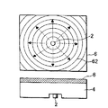
これら輝度分布の不均一性の原因は、導光体の光入射端面に配置した個々のLEDから発せられる光が指向性を持っており、さらに導光体に入射する際の屈折作用により導光体に入射した光の広がりが比較的小さくなるためであり、図13に示したように、LEDの両端側の領域に暗い部分が発生する。特に、消費電力の低減を図るために、使用するLEDの個数を少なくしたり、LEDを導光体に近接して設置する場合には、暗い部分の発生が顕著になる。このように、一次光源として点状光源を用いる従来のバックライトでは、消費電力の低減と輝度の均一性の維持とを両立させることは困難であった。
【0006】
また、一次光源として冷陰極間等の線状光源を使用したバックライトにおいても、線状または棒状の一次光源の両端部に近い導光体コーナー部や、導光体の光入射端面に隣接する側端面の近くの領域に十分な光量が到達せず、これらの部分や領域の輝度が低下しやすいという問題がある。このような入射面近傍部の暗部等を解消する方法として、例えば特開平10−153778号公報には、導光体の入射面近傍部の表面を粗面化する方法が提案されているが、LED等の点状光源を一次光源として用いたバックライトでは、このような方法では十分に前記のような暗い部分を解消することはできなかった。
【0007】
そこで、本発明の目的は、以上のような面光源装置の低消費電力化のための少ない数の点状一次光源の使用等に伴う輝度の均斉度の不均一を解消して、高品位の面光源装置を提供することにある。
【0008】
【課題を解決するための手段】
すなわち、本発明の面光源装置用導光体は、略点状の一次光源からの光を入射する光入射端面と入射光を出射する光出射面とを有する矩形状の導光体において、前記光入射端面の少なくとも一部に前記光出射面からその反対側の面の方向に延び、その断面が非対称形状であり、少なくとも一部が曲線である複数のレンズ列が略平行に形成されていることを特徴とするものである。また、本発明の面光源装置は、上記のような導光体と、該導光体の光出射面側に配置された光偏向素子とからなることを特徴とするものである。
【0009】
【発明の実施の形態】
以下、図面を参照して本発明の実施の形態を詳細に説明する。
【0010】
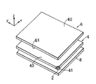
図1は、本発明による面光源装置の一つの実施形態を示す分解斜視図である。図1に示されているように、本実施形態の面光源装置は、略点状の一次光源としてのLED2と、該LED2から発せられる光を光入射端面から入射させ導光して光出射面から出射させるXY面内の矩形板状の導光体4と、該導光体4に隣接配置される光偏向素子6及び光反射素子8とを備えている。
【0011】
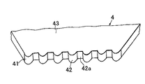
導光体4は、上下2つの主面と該主面の外周縁どうしを連ねる端縁を有し、端縁の一つのコーナー部を切り欠き光入射端面とし、LED2が配置されている。この導光体4の入射端縁には、LED2が配置される位置に相当する光入射端面41が形成されている。光入射端面41には、図2に示すように少なくともLED2と対向する箇所に該光出射面からその反対側の面の方向に延び、その断面が非対称形状であり、少なくとも一部が曲線である複数のレンズ列42が略平行に形成されている。光入射端面41が平面である場合には導光体4に入射する際の屈折作用により導光体4に入射した光の配光分布は、LED2から発せられる光の分布より狭くなっていたが、このようなレンズ列42を光入射端面41に形成することにより、導光体4に入射した光の配光分布を広げることができる。また、レンズ列42の断面形状を非対称にすることで各方向に出射する光量を調節することができ、導光体4の光出射面全体での輝度の均斉度を高めることができる。さらに、レンズ列42は、多様な屈折角を生み出し導光体4に入射した光の配光分布を効率良く広げるために、少なくともその一部が曲面で形成される。
【0012】
レンズ列42のピッチがLED3に対して大きすぎるとレンズ列42の屈折作用がLED2との相対的位置関係によって一意的に決まってしまうため、その位置関係による光線の広がりによる斑が視認されてしまうため、レンズ列42のピッチは小さい方が好ましいが、あまり小さすぎると形状転写が困難になったり、形状精度の低下を招くことから、10〜200μmの範囲とすることが好ましく、より好ましくは20〜100μm、さらに好ましくは30〜60μmの範囲である。
【0013】
レンズ列42の好ましい断面形状としては、少なくとも2つの異なる曲線の組み合わせからなる非対称形状であり、例えば、異なる2つの曲面を組み合わせた形状、異なる2つ以上の球面あるいは非球面形状の一部を組み合わせた形状、異なる2つ以上の球面の一部と非球面形状の一部を組み合わせた形状、円弧と楕円の一部から構成された形状、略四分の一円と略四分の一楕円を組み合わせた形状、異なる長軸および短軸を持つ二つの略四分の一楕円を組み合わせた形状などが挙げられる。なお、略四分の一円および略四分の一楕円とは、円および楕円全体の概ね四分の一の形状をいう。レンズ列42の断面形状は、導光体4に入射した光の所望の配光分布によって決定され、例えば、広い配光分布が必要となる場合には光の進行方向を短軸とするような楕円形状とすることが好ましい。
【0014】
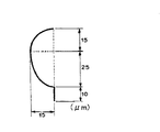
具体的には、図10〜12に示したようなレンズ形状のものが挙げられる。図10は、一つのレンズ単位が、長径が20μmで短径が15μmの四分の一楕円と、長径が30μmで短径が15μmの四分の一楕円を組み合わせた異なる長軸および短軸を持つ二つの略四分の一楕円を組み合わせた形状である。図11は、一つのレンズ単位が、半径15μmの四分の一円と、長径が25μmで短径が15μmの四分の一楕円とを組み合わせた形状のレンズと、幅10μmの平面とからなるものである。図12は、一つのレンズ単位が、長径が17μmで短径が16μmの四分の一楕円と、長径が34μmで短径が17μmの四分の一楕円を組み合わせた形状で光入射端面の一部を平面とした形状の複数のレンズと、レンズ形成面となす角度が21度の平面とからなるものである。なお、レンズ列42の断面形状はその一部が直線であってもよい。このようにレンズ列42の断面形状の一部を直線にすることにより、レンズ列42の形状の賦形安定性が向上し、導光体4に入射した光の配光分布の広がり容易に制御できる。
【0015】
また、本発明においては、図3に示すように隣接するレンズ列42の間に平面部分や曲面部分を形成してもよい。レンズ列42間に形成する平面部分等の長さを調整し光の配光分布を調整することができ、輝度の均一化を図るための最適な配光分布を得ることができる。この場合、形成する平面や曲面の幅は、レンズ列42の配光分布を広げる効果とのバランスからレンズ列42のピッチより小さいことが好ましく、例えば5〜100μm程度の幅とすることが好ましく、より好ましくは5〜50μm、さらに好ましくは7〜30μmの範囲である。断面形状が直線をなしている部分は図5に示すようにレンズ端でもよい。さらに、レンズ列42は、配置されたLED2に対向する部分だけに形成したり、図4に示すように光入射端面の一部に形成し他の部分は平面としてもよい。この場合、光入射端面の長さに対する平面部分の長さの割合は30%以下とすることが好ましく、より好ましくは15〜20%の範囲である。
【0016】
導光体4は、2つの主面の一方の主面(図では上面)が光出射面43とされ、他方の主面が裏面とされている。この光出射面43または裏面の少なくとも一方の主面には、導光体4内を導光する光を光出射面43に対して傾斜した方向(即ちXY面に対して傾斜した方向)に光を出射させる指向性光出射機構を備えている。指向性光出射機構としては、例えば、導光体4の光出射面43および裏面の少なくとも1つの表面に凹凸形状を形成したり、あるいは、導光体4中に基材と屈折率が異なる構造を形成する、例えば基材と屈折率の異なる光拡散性微粒子を含有させることにより指向性光出射機構を形成することもできる。これら指向性光出射機構は、複数の指向性光出射機構を組み合わせて導光体4に形成することもできる。導光体4に入射した光は、このような指向性光出射機構によって、導光体4中を伝搬する間に光出射面43への入射角が変化し、光出射面43への入射角が臨界角より小さくなった場合に光出射面43から出射される。
【0017】
導光体4の表面を凹凸形状とすることにより指向性光出射機構を形成する場合としては、プリズム列、レンチキュラーレンズ列、V字状溝等の多数のレンズ列を並列に形成したレンズ面、あるいは、粗面(マット面)とすること等が挙げられる。このような指向性光出射機構を設けた導光体4は、光出射面43から出射する出射光の出射光分布におけるピーク出射光の方向が光出射面43と10〜50度の角度であり、出射光分布の半値幅が10〜40度であることが好ましい。
【0018】
本発明において、指向性光出射機構としての粗面やレンズ面は、ISO4287/1−1984による平均傾斜角θaが2〜12度の範囲とすることが好ましく、より好ましくは3〜10度の範囲である。これは、平均傾斜角θaが2度未満では、導光体4の光出射率が小さくなり光の出射量が不十分となり、輝度が低下する傾向にあるためであり、逆に、平均傾斜角θaが12度を超えると、導光体4の光出射率が大きく一次光源2の近傍での出射光量が大きくなり、光出射面43内での輝度の均一性が低下する傾向にあるためである。本発明において、粗面やレンズ面の平均傾斜角θaは、導光体4の表面内で均一としてもよいし、連続的に、断続的にあるいは部分的に変化させてもよい。例えば、光出射面43内での輝度の均一性を向上させるためには、一次光源2から遠くなるに従って平均傾斜角θaを大きくすることが好ましい。また、光出射面43内で部分的に輝度が低下する箇所が存在する場合には、その部分の平均傾斜角θaを大きくしたり、逆に部分的に輝度が高くなる箇所が存在する場合には、その部分の平均傾斜角θaを小さくしたりすることにより、出射光量を部分的に制御して輝度の均一化を図ることもできる。
【0019】
導光体4に形成される粗面やレンズ面の平均傾斜角θaは、ISO4287/1−1984に従って、触針式表面粗さ計を用いて粗面形状を測定し、測定方向の座標をxとして、得られた傾斜関数f(x)から次の(1)式および(2)式を用いて求めることができる。ここで、Lは測定長さであり、Δaは平均傾斜角θaの正接である。
【0020】
【数1】

【0021】
本発明においては、一次光源2としてLED等の略点状光源を使用するため、導光体4に入射した光は、光出射面43と略同一の平面内において一次光源2を略中心とした放射状に導光体4中を伝搬する。このような放射状に伝搬する光に対して、弧状に形成したレンズ列(弧状レンズ列)を一次光源2を取り囲むように略弧状に並列して配置することにより、導光体4中を放射状に伝搬する光の殆どが弧状レンズ列に対して略垂直方向に入射することになるため、その伝搬方向に関わらず効率よく所望の方向に出射させることができ、伝搬方向を維持しやすくなるとともに、導光体4の光出射面43の全領域で出射光を効率良く特定の方向に向けることができ、輝度の均一性を向上させることができる。弧状レンズ列は、導光体4中を伝搬する光の分布に応じてその弧状の程度を選定し、導光体4中を放射状に伝搬する光の殆どが弧状レンズ列に対して垂直方向に入射するようにすることが好ましい。このような弧状レンズ列としては、断面形状が三角形状、弧状、半円状、多角形状等の形状のものを形成することができる。
【0022】
指向性光出射機構としてこのような弧状レンズ列を形成する場合、形成する弧状レンズ列の径方向の分布は、連続して形成することもできるし、隣接する弧状レンズ列の間に平坦部を介して離散的にすることもできる。弧状レンズ列を連続して形成した場合、弧状レンズ列から出射した後に、隣接する弧状レンズ列に入射する光が存在する場合があり、このような光が多量に存在する場合には導光体4から出射する出射光の出射光分布の乱れが大きくなり、光偏向素子6によって所望の方向に偏向されない光が多くなることにより、輝度の低下を招く場合がある。このような場合には、弧状レンズ列を離散的に形成することにより、隣接する弧状レンズ列に入射する光を低減することができ、導光体4から出射する出射光からの出射光分布の乱れによる輝度の低下を抑止することができる。
【0023】
一次光源としてのLED2を本実施形態のように導光体4の1つのコーナー部に配置した場合には、LED2の光の指向性の方向と導光体4の長辺とのなす角度を図5に示すように37〜45度の範囲とすることが好ましく、さらに好ましくは39〜42度の範囲である。これは、LED2の光の指向性の方向と導光体4の長辺とのなす角が37度未満であると、導光体4の短辺とのなす角度が大きくなり、LED2の光の指向性の方向と短辺との間の領域の輝度むらを防ぐことが困難となる傾向にあるためであり、この角度が45度を超えるとLED2の光の指向性の方向と短辺との間の領域が長辺との間の領域に比べ増大するため、LED2の光の指向性の方向と短辺との間の領域の輝度減少を防ぐことが困難となる傾向にあるためである。
【0024】
このようにLED2が導光体4のコーナー部に配置された場合には、図6、7に示したように導光体4の光出射面43にLED2を取り囲むようにして多数のレンズ列を略弧状に並列して形成することが好ましい。なお、本発明においては、図7に示したように導光体4として光出射面43が略台形形状をなし、その底辺がなす1つのコーナー部にLED2を配置することもできる。
【0025】
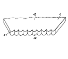
本発明においては、一次光源としてのLED2の配置は、本実施形態のようにコーナー部に限らず、図8、9に示したような配置をすることもできる。図8は、LED2が導光体4の裏面に設けられた凹部または貫通孔内に導光体4との間に空気層または透明物質を介して設置され、導光体4の光出射面43にLED3を取り囲むようにして多数のレンズ列を略円弧状に並列して形成したものである。図9は、導光体4の1つの端縁に複数個のLED2を配置し、導光体4の光入射端面41のLED2と対向する部分にレンズ列42が形成されている。この場合には、光入射端面41の中央付近に位置するLEDと対向する位置には左右対称の断面形状を有するレンズ列422を形成し、光入射端面41の両端付近に位置するLEDと対向する位置には左右非対称の断面形状を有するレンズ列421を形成することにより、導光体4の光出射面全体で輝度の均斉度を向上させることができる。
【0026】
光偏向素子6は、導光体4の光出射面43上に配置されている。光偏向素子6の2つの主面は、それぞれ全体としてXY面と平行に位置する。2つの主面のうち一方(導光体の光出射面43側に位置する主面)は入光面61とされており、他方が出光面62とされている。光偏向素子6は、導光体4からの出射光を目的の方向に偏向(変角)させる機能を果たすものであり、少なくとも一方の面に2つの面を有する多くのプリズム列が平行に配列して形成されたレンズ面を有するレンズシート等を使用することができる。
【0027】
本発明においては、一次光源2としてLED等の略点状光源を使用しているため、導光体4に入射した光は、光出射面43と同一の平面内において一次光源2を略中心とした放射状に導光体4中を伝搬し、光出射面43から出射する出射光も同様に一次光源2を中心とした放射状に出射する。このような放射状に出射する出射光を、その出射方向に関わらず効率よく所望の方向に偏向させるためには、光偏向素子6に形成するプリズム列を一次光源2を取り囲むように略弧状に並列して配置する。このように、プリズム列を一次光源2を取り囲むように略弧状に並列して配置することにより、光出射面43から放射状に出射する光の殆どが光偏向素子6のプリズム列に対して垂直方向に入射するため、導光体4の光出射面43の全領域で出射光を効率良く特定の方向に向けることができ、輝度の均一性を向上させることができる。
【0028】
光偏向素子6に形成する略弧状のプリズム列は、導光体4中を伝搬する光の分布に応じてその弧状の程度を選定し、光出射面43から放射状に出射する光の殆どが光偏向素子6のプリズム列に対して垂直方向に入射するようにすることが好ましい。具体的には、LED等の点状光源を略中心とした同心円状に円弧の半径が少しずつ大きくなるように並列して配置されたものが挙げられ、プリズム列の半径の範囲は、面光源システムにおける点状光源の位置と、液晶表示エリアに相当する面光源の有効エリアとの位置関係や大きさによって決定される。
【0029】
また、光偏向素子6に形成されるプリズム列のパターンは、一次光源2の配置方法に応じて、光出射面43から放射状に出射する光の殆どが光偏向素子6のプリズム列に対して略垂直方向に入射するようなパターンとなるように、適宜設定することができる。さらに、光偏向素子6に形成するプリズム列は、導光体4の光出射面43に対面して光偏向素子6の入光面61に形成してもよいし、出光面62に形成してもよし、入光面61と出光面62の両面に形成してもよい。導光体4からの指向性の高い出射光を効率よく所望の方向に偏向させ、高い輝度を得るためには、光偏向素子6の入光面61にプリズム列を形成することが好ましい。
【0030】
入光面61にプリズム列を形成した光偏向素子6を導光体4の光出射面43に配置した場合には、光出射面43から出射した出射光は、プリズム列の一次光源2に近い方の面から光偏向素子6に入射し、一次光源2に遠い方の面で内面反射し所望の方向に偏向された後、光偏向素子6の出光面62から出射する。このため、導光体4の光出射面43から出射した出射光の指向性をほぼ維持した状態でその出射方向を所望の方向に変えることができ、光の利用効率が高くなるとともに、輝度の高い面光源システムとすることができる。
【0031】
導光体4の光出射面43から出射する出射光は、出射光分布のピ−ク光が光出射面43に対して10〜50度傾いた方向であるため、プリズム列の一次光源2から遠い方の面と光偏向素子6の基準平面のなす角度は40〜80度であることが好ましく、より好ましくは50〜65度、さらに好ましくは55〜65度である。これは、一次光源2から遠い方の面と光偏向素子6の基準平面のなす角度をこの範囲とすることにより、このような指向性を持つ導光体4からの出射光を、光偏向素子6の出光面62の法線方向の近傍に偏向して出射することができるためである。ここで、光偏向素子6の基準平面とは、光偏向素子6のプリズム列が形成された面が平滑であると仮定した時の平面とする。
【0032】
一方、導光体4中を伝搬する光の一部は、導光体4の末端まで到達し、その端面で反射して戻ってくる光が存在する。このような光は、導光体4の光入射面に向かって導光体4中を伝搬し、導光体4に形成された指向性光出射機構により光出射面43から出射される。このような出射光は、光偏向素子6の一次光源2から遠い側のプリズム面から入射し、一次光源2に近い側のプリズム面で内面反射し所望の方向に偏向た後され、光偏向素子6の出射光面62から出射する。このような出射光も、出射光分布のピ−ク光が光出射面43に対して10〜50度傾いた方向であるため、このような出射光が比較的多い場合には、プリズム列の一次光源2に近い方のプリズム面と光偏向素子6の基準平面のなす角度も、一次光源2から遠い方のプリズム面と同様に40〜80度であることが好ましく、より好ましくは50〜65度、さらに好ましくは55〜65度である。
【0033】
光偏向素子6の基準平面に対する2つのプリズム面のなす角度は同一としてもよく、異ならせることもできる。両角度を異ならせる場合には、その差が10度以下であることが好ましく、より好ましくは5度以下、さらに好ましくは2度以下である。
【0034】
本発明において、携帯電話や携帯情報端末等のような携帯用電子機器の面光源システムのように、消費電力の低減化と高輝度化の要求が非常に高い用途では、光偏向素子6に形成するプリズム列の断面形状を、プリズム面を凸状の曲面あるいは多角面形状とすることにより、プリズム面で内面反射する際に所望方向へ集中するように偏向させることができ、より指向性の高い集中光として出射されるため、消費電力あたりの輝度を高めることができ、低消費電力化および高輝度化をより高めることができる。
【0035】
本発明の導光体4及び光偏向素子6は、光透過率の高い合成樹脂から構成することができる。このような合成樹脂としては、メタクリル樹脂、アクリル樹脂、ポリカーボネート系樹脂、ポリエステル系樹脂、塩化ビニル系樹脂、環状ポリオレフィン樹脂が例示できる。特に、メタクリル樹脂が、光透過率の高さ、耐熱性、力学的特性、成形加工性に優れており、最適である。このようなメタクリル樹脂としては、メタクリル酸メチルを主成分とする樹脂であり、メタクリル酸メチルが80重量%以上であるものが好ましい。導光体4及び光偏光素子6の粗面の表面構造やプリズム列等の表面構造を形成するに際しては、透明合成樹脂板を所望の表面構造を有する型部材を用いて熱プレスすることで形成してもよいし、スクリーン印刷、押出成形や射出成形等によって成形と同時に形状付与してもよい。また、熱あるいは光硬化性樹脂等を用いて構造面を形成することもできる。更に、ポリエステル系樹脂、アクリル系樹脂、ポリカーボネート系樹脂、塩化ビニル系樹脂、ポリメタクリルイミド系樹脂等からなる透明フィルムあるいはシート等の透明基材上に、活性エネルギー線硬化型樹脂からなる粗面構造またレンズ列配列構造を表面に形成してもよいし、このようなシートを接着、融着等の方法によって別個の透明基材上に接合一体化させてもよい。活性エネルギー線硬化型樹脂としては、多官能(メタ)アクリル化合物、ビニル化合物、(メタ)アクリル酸エステル類、アリル化合物、(メタ)アクリル酸の金属塩等を使用することができる。
【0036】
光反射素子8としては、例えば表面に金属蒸着反射層を有するプラスチックシートを用いることができる。また、導光体4の側端面(光入射端面41を除く)にも反射部材を付することが好ましい。
【0037】
一次光源2としては、消費電力等の点からLED光源が好ましいが、ハロゲンランプ等のような他の略点状の光源を用いることもできる。また、略点状の一次光源2としては、単色光のもの、赤、緑、青の3原色の波長の光を有する白色光源等を用いることができる。本発明においては、このような一次光源2として略点状の光源を1個または複数個使用することができる。また、1つのコーナー部または端面に複数の略点状の光源を近接して配置する場合には、複数の略点状の光源をアレイ化したLEDアレイ等を点状光源として使用することができる。
【0038】
一次光源2としては、目的や要求特性に応じて、最適の発光パターン(出射光分布)のものを用いることが好ましい。一般的には、一次光源2の前方の輝度が他の部分より高くなる現象を緩和するために、導光体4の光出射面43に平行な方向(a方向)での発光パターンの広がりは大きいことが好ましく、発光パターンのピーク半値幅が120〜180度程度であるものが好ましい。導光体4の端面に一次光源2を設置する場合は、a方向の広がりが大きい発光パターンのものを使用することが好ましく、ピーク半値幅が140〜180度程度であるものが好ましい。また、導光体4のコーナー部に一次光源2を設置する場合は、導光体4中に入射した光が導光体4のa方向において全面に向かって広がることが好ましく、入射した光の広がり角度が導光体4の面の広がりにほぼ一致することが好ましい。このため、光を入射する導光体2のコーナーの角度が90度である場合には一次光源2のa方向の発光パターンのピーク半値幅が60〜120度程度であるものが好ましく、コーナーの角度が45度である場合には一次光源2のa方向の発光パターンのピーク半値幅が20〜70度程度であるものが好ましい。
【0039】
また、一次光源2の光出射面43に垂直な方向(b方向)の発光パターンは、そのピーク半値幅が10〜120度程度であることが好ましい。これは、b方向が広すぎると光は一次光源2の近傍で出射しやすくなり輝度の均一性が低下する傾向にあり、b方向の発光パターンが狭すぎると導光体4からの出射率が小さくなり輝度が低下する傾向にあるためである。
【0040】
【実施例】
以下、実施例によって本発明を具体的に説明する。
実施例1
導光体の作製
鏡面仕上げをした48mm×34mm、厚さ3mmの真鍮板の表面に、ピッチ30μmで、断面形状が頂角160度の断面二等辺三角形で、48mm×34mmの四角形状の1つのコーナー近傍を中心とした円弧状プリズム列を同心円状に形成し、隣接する円弧状プリズム列間に30〜200μmの平坦部を中心部より徐々に間隔が狭くなるように形成した円弧状プリズムパターンを40mm×30mmの有効領域に切削加工した金型を得た。得られた金型と、鏡面仕上げをした48mm×34mm、厚さ3mmの真鍮板を用いて射出成形を行い、長辺48mm、短辺34mm、厚み0.8mmの矩形の導光板を得た。射出成形の材料としては、ポリメチルメタクリレ−トを用いた。
【0041】
得られた導光体は、一方の面が平滑面で、他方の面に図6に示したような円弧状プリズムパターンが形成されていた。この導光体の円弧状プリズム列の中心となるコーナー部を端面長さ4mmの平面状に切り欠き部を形成し光入射端面とした。この光入射端面全面に、図11に示したような半径15μmの四分の一円と、長径が25μmで短径が15μmの四分の一楕円とを組み合わせた形状のレンズ列と、幅10μmの平面とからなるレンズ列パターン形成した金型を用いて加熱転写した。
【0042】
光偏向素子の作製
鏡面仕上げをした48mm×34mm、厚さ3mmの真鍮板の表面に、ピッチ50μmで、断面形状が65.4度の頂角を挟む2つの傾斜面が曲率半径400μmの凸状曲面である略二等辺三角形で、48mm×34mmの四角形状の1つのコーナー近傍を中心とした円弧状プリズム列を同心円状に並列して連設した円弧状プリズムパターンを切削加工した金型を得た。得られた金型にアクリル系紫外線硬化性組成物を注入し、188μmのポリエステルフィルム(東洋紡社製A4000、屈折率1.600)を重ね合わせた後、高圧水銀ランプを用いてポリエステルフィルムを通して紫外線を照射しアクリル系紫外線硬化性組成物を硬化し、金型から剥離しプリズムシートを得た。得られたプリズムシートは、ポリエステルフィルムの片面に、屈折率1.528の紫外線硬化樹脂からなり、ピッチ50μmで、65.4度の頂角を挟む2つのプリズム面が曲率半径400μmの凸状曲面である略二等辺三角形で、1つのコーナー近傍を中心とする同心円状の円弧状プリズム列が並列して連設した円弧状プリズムパターンが形成されていた。
【0043】
面光源システムの作製
得られた導光体の円弧状プリズムパターンが形成された面側に光拡散反射フィルム(辻本電機製作所社製SU−119)を設置し、導光体の光出射面となる平滑面側に、得られたプリズムシ−トを円弧状プリズムパターンを形成した面が導光体側となり、形成した円弧状プリズム列の中心となるコーナー部が導光体の切り欠き部と重なるように設置した。また、導光体の切り欠き部には、導光体の光出射面と平行方向のピーク半値幅が115度(±57.5度)、垂直方向のピーク半値幅110度(±55度)のLED光源1個を、LED光源の指向性の方向と導光体の長辺とのなす角が40度となるように設置し、15mAの電流を流した。
【0044】
評価
得られた面光源システムを点灯し観察したところ、輝度むらの発現はほとんど視認されない良好な外観であった。
【0045】
【発明の効果】
以上のように、本発明によれば、比較的少ない数の点状光源を一次光源として使用した場合であっても、輝度むらのない均斉度のとれた高品位の面光源装置を提供することができる。
【図面の簡単な説明】
【図1】本発明の面光源装置を示す分解斜視図である。
【図2】本発明の導光体の光入射端面の拡大斜視図である。
【図3】本発明の導光体の光入射端面の拡大斜視図である。
【図4】本発明の導光体の光入射端面の拡大斜視図である。
【図5】導光体に対する一次光源の位置を示す説明図である。
【図6】本発明の面光源装置の一実施態様を示す斜視図ある。
【図7】本発明の面光源装置の一実施態様を示す斜視図ある。
【図8】本発明の面光源装置の一実施態様を示す斜視図ある。
【図9】本発明の面光源装置の一実施態様を示す斜視図ある。
【図10】本発明の光入射端面に形成するレンズ列の形状を示す断面図である。
【図11】本発明の光入射端面に形成するレンズ列の形状を示す断面図である。
【図12】本発明の光入射端面に形成するレンズ列の形状を示す断面図である。
【図13】従来の面光源装置における導光体中での光の拡がり方を示す説明図である。
【符号の説明】
2 LED
4 導光体
41 光入射端面
42 光入射端面に形成されたレンズ列
421 非対称レンズ列
422 対称レンズ列
43 光出射面
6 光偏向素子
61 入光面
62 出光面
8 光反射素子[0001]
TECHNICAL FIELD OF THE INVENTION
INDUSTRIAL APPLICABILITY The present invention is used as a liquid crystal display device used for a notebook personal computer or a liquid crystal television, a display of a portable electronic device such as a mobile phone, a portable information terminal, a portable game machine, and an indicator of various electric / electronic devices. The present invention relates to a surface light source device suitable for a relatively small liquid crystal display device using a substantially point-like primary light source such as an LED and a light guide used therein, and more particularly to a high-quality illumination having a high degree of uniformity of luminance. The present invention relates to a surface light source device that can be provided.
[0002]
Problems to be solved by the prior art and the invention
In recent years, liquid crystal display devices have been widely used as monitors for portable notebook personal computers and the like, or as display units for liquid crystal televisions and video-integrated liquid crystal televisions, and in various other fields. The liquid crystal display device basically includes a backlight unit and a liquid crystal display element unit. As a backlight unit, an edge light type backlight is frequently used from the viewpoint of downsizing of a liquid crystal display device. Conventionally, as a backlight, at least one end face of a rectangular plate-shaped light guide is used as a light incidence end face, and a linear or rod-shaped primary light source such as a straight tube fluorescent lamp is arranged along the light incidence end face. And introducing light emitted from the primary light source into the inside of the light guide from the light incident end face of the light guide and emitting the light from one of the two main surfaces of the light guide. Is widely used.
[0003]
On the other hand, in recent years, portable electronic devices such as mobile phones, portable information terminal devices and portable game machines, or liquid crystal display devices having relatively small screen dimensions such as indicators of various electric and electronic devices have been reduced in size and power consumption. Reduction is desired. Therefore, in order to reduce power consumption, a light emitting diode (LED) which is a point light source is used as a primary light source of the backlight. As a backlight using an LED as a primary light source, for example, as described in JP-A-7-270624, a plurality of LEDs are used to exhibit the same function as that using a linear primary light source. They are arranged one-dimensionally along the light incident end face of the light guide. By using a primary light source based on a one-dimensional array of a plurality of LEDs in this manner, it is possible to obtain a required light amount and uniformity of luminance distribution over the entire screen.
[0004]
Further, in the case of a small liquid crystal display device, further reduction in power consumption is required, and in order to meet this demand, it is necessary to reduce the number of LEDs used. However, if the number of LEDs is reduced, the distance between the light emitting points becomes longer, so that the area of the light guide close to the area between the adjacent light emitting points is enlarged, and light is emitted from this light guide area in a required direction. The light intensity decreases. This leads to non-uniform luminance distribution in the viewing direction on the light emitting surface of the surface light source device (that is, non-uniform luminance uniformity). In Japanese Patent Publication No. 7-27137, a light guide having a rough light exit surface is used, and a prism sheet in which a large number of prism rows are arranged is formed such that the prism surface faces the light guide. A method has been proposed in which the distribution of emitted light is narrowed in order to reduce the power consumption of the backlight and to reduce the brightness as much as possible, by arranging the light on the light emitting surface. However, in such a backlight, although high brightness can be obtained with low power consumption, when the number of LEDs used is reduced, the unevenness of the brightness distribution of the light emitted from the light guide is easily recognized through the prism sheet. Met.
[0005]
The cause of the non-uniformity of the luminance distribution is that the light emitted from each LED arranged on the light incident end face of the light guide has directivity, and furthermore, the light is guided by the refraction effect when entering the light guide. This is because the spread of the light that has entered the body is relatively small, and as shown in FIG. 13, dark portions are generated in the regions on both ends of the LED. In particular, when the number of LEDs to be used is reduced or the LEDs are installed close to the light guide in order to reduce power consumption, dark portions become noticeable. As described above, in the conventional backlight using a point light source as the primary light source, it has been difficult to achieve both reduction in power consumption and maintenance of uniformity of luminance.
[0006]
Further, even in a backlight using a linear light source such as between cold cathodes as a primary light source, a light guide corner near the both ends of a linear or rod-shaped primary light source, or adjacent to a light incident end face of the light guide. There is a problem that a sufficient amount of light does not reach a region near the side end surface, and the luminance of these portions and regions is likely to be reduced. As a method of eliminating such a dark portion near the incident surface, for example, Japanese Patent Application Laid-Open No. H10-153778 proposes a method of roughening the surface of the light guide near the incident surface. In a backlight using a point light source such as an LED as a primary light source, such a method cannot sufficiently eliminate the dark part as described above.
[0007]
Therefore, an object of the present invention is to eliminate unevenness in brightness uniformity due to the use of a small number of point-like primary light sources for reducing power consumption of the surface light source device as described above, and to achieve high quality. An object of the present invention is to provide a surface light source device.
[0008]
[Means for Solving the Problems]
That is, the light guide for a surface light source device of the present invention is a rectangular light guide having a light incident end surface for receiving light from a substantially point-shaped primary light source and a light exit surface for emitting incident light. At least a part of the light-incident end face extends from the light-emitting face in the direction of the opposite face, has a cross-section that is asymmetric, and has a plurality of lens rows that are at least partially curvilinearly formed substantially in parallel. It is characterized by the following. Further, a surface light source device of the present invention is characterized by comprising the above light guide and a light deflecting element arranged on the light exit surface side of the light guide.
[0009]
BEST MODE FOR CARRYING OUT THE INVENTION
Hereinafter, embodiments of the present invention will be described in detail with reference to the drawings.
[0010]
FIG. 1 is an exploded perspective view showing one embodiment of a surface light source device according to the present invention. As shown in FIG. 1, the surface light source device of the present embodiment includes an
[0011]
The
[0012]
If the pitch of the
[0013]
The preferred cross-sectional shape of the
[0014]
Specifically, those having a lens shape as shown in FIGS. FIG. 10 shows that one lens unit has different major and minor axes obtained by combining a quarter ellipse with a major axis of 20 μm and a minor axis of 15 μm and a quarter ellipse with a major axis of 30 μm and a minor axis of 15 μm. It has a shape combining two substantially quarter ellipses. FIG. 11 shows that one lens unit includes a lens having a shape obtained by combining a quarter circle having a radius of 15 μm, a quarter ellipse having a major axis of 25 μm and a minor axis of 15 μm, and a plane having a width of 10 μm. Things. FIG. 12 shows that one lens unit is a combination of a quarter ellipse having a major axis of 17 μm and a minor axis of 16 μm and a quarter ellipse having a major axis of 34 μm and a minor axis of 17 μm. The lens comprises a plurality of lenses having a flat portion, and a plane having an angle of 21 degrees with the lens forming surface. The cross-sectional shape of the
[0015]
Further, in the present invention, a plane portion or a curved portion may be formed between
[0016]
One of the two main surfaces (the upper surface in the figure) of the
[0017]
When the directional light emitting mechanism is formed by making the surface of the
[0018]
In the present invention, the average inclination angle θa according to ISO 4287 / 1-1984 is preferably in the range of 2 to 12 degrees, and more preferably in the range of 3 to 10 degrees, for the rough surface or the lens surface as the directional light emitting mechanism. It is. This is because if the average inclination angle θa is less than 2 degrees, the light emission rate of the
[0019]
The average inclination angle θa of the rough surface or the lens surface formed on the
[0020]
(Equation 1)
[0021]
In the present invention, since a substantially point-like light source such as an LED is used as the primary
[0022]
When such an arc-shaped lens array is formed as a directional light emitting mechanism, the radial distribution of the formed arc-shaped lens array can be formed continuously, or a flat portion can be formed between adjacent arc-shaped lens arrays. Can be discrete via When the arc-shaped lens array is formed continuously, there is a case where there is light incident on an adjacent arc-shaped lens array after exiting from the arc-shaped lens array. Dispersion of the outgoing light of the outgoing light emitted from the
[0023]
When the
[0024]
When the
[0025]
In the present invention, the arrangement of the
[0026]
The
[0027]
In the present invention, since a substantially point light source such as an LED is used as the primary
[0028]
The substantially arc-shaped prism array formed on the
[0029]
Also, the pattern of the prism array formed on the
[0030]
When the
[0031]
The light emitted from the
[0032]
On the other hand, a part of the light propagating in the
[0033]
The angle formed by the two prism surfaces with respect to the reference plane of the
[0034]
In the present invention, when the demand for reduction of power consumption and high brightness is extremely high, such as a surface light source system of a portable electronic device such as a mobile phone or a portable information terminal, the
[0035]
The
[0036]
As the light reflection element 8, for example, a plastic sheet having a metal deposition reflection layer on the surface can be used. Further, it is preferable that a reflection member is also provided on the side end surface of the light guide 4 (excluding the light incident end surface 41).
[0037]
As the primary
[0038]
As the primary
[0039]
Further, it is preferable that the emission pattern in the direction (b direction) perpendicular to the
[0040]
【Example】
Hereinafter, the present invention will be specifically described with reference to examples.
Example 1
Fabrication of light guide
On the surface of a mirror-finished 48 mm x 34 mm, 3 mm thick brass plate, with a pitch of 30 µm, a cross-sectional shape is an isosceles triangle with a vertex angle of 160 degrees, centered around one corner of a square of 48 mm x 34 mm An arcuate prism pattern is formed concentrically, and a flat portion of 30 to 200 μm is formed between adjacent arcuate prism lines so as to gradually narrow the interval from the center. A die cut in the area was obtained. Injection molding was performed using the obtained mold and a mirror-finished 48 mm × 34 mm, 3 mm thick brass plate to obtain a rectangular light guide plate having a long side of 48 mm, a short side of 34 mm, and a thickness of 0.8 mm. Polymethyl methacrylate was used as a material for injection molding.
[0041]
The resulting light guide had a smooth surface on one side and an arc-shaped prism pattern as shown in FIG. 6 formed on the other side. A corner portion of the light guide, which is the center of the arc-shaped prism array, was formed as a light incident end surface by forming a notch in a plane having an end surface length of 4 mm. A lens array having a shape obtained by combining a quarter circle having a radius of 15 μm as shown in FIG. 11, a quarter ellipse having a major axis of 25 μm and a minor axis of 15 μm, and a width of 10 μm, as shown in FIG. Heat transfer was performed using a mold having a lens array pattern formed of the flat surface.
[0042]
Fabrication of light deflection element
On a 48 mm × 34 mm mirror-finished brass plate having a thickness of 3 mm, approximately two convex surfaces having a pitch of 50 μm and a cross-sectional shape having an apex angle of 65.4 degrees are convex curved surfaces having a radius of curvature of 400 μm. A mold was obtained by cutting an arc-shaped prism pattern in which arc-shaped prism rows each having an isosceles triangle and being arranged concentrically in parallel with arc-shaped prism rows centered on one corner of a square of 48 mm × 34 mm. An acrylic UV curable composition was injected into the obtained mold, and a 188 μm polyester film (A4000, manufactured by Toyobo Co., refractive index: 1.600) was superimposed. Ultraviolet rays were passed through the polyester film using a high-pressure mercury lamp. Irradiation was performed to cure the acrylic ultraviolet curable composition, and the composition was separated from the mold to obtain a prism sheet. The obtained prism sheet is made of a UV curable resin having a refractive index of 1.528 on one side of a polyester film, and has a pitch of 50 μm, and two prism faces sandwiching a 65.4 degree apex angle have a convex curved surface with a radius of curvature of 400 μm. In this case, an arc-shaped prism pattern was formed in which substantially concentric arc-shaped prism rows centered around one corner were arranged in parallel.
[0043]
Fabrication of surface light source system
A light diffusing reflection film (SU-119, manufactured by Tsujimoto Electric Co., Ltd.) was installed on the surface of the obtained light guide on which the arc-shaped prism pattern was formed, and on the smooth surface side of the light guide, which became the light emission surface, The obtained prism sheet was placed so that the surface on which the arc-shaped prism pattern was formed was on the light guide side, and the corner portion, which was the center of the formed arc-shaped prism row, overlapped the cutout portion of the light guide. In the notch of the light guide, the peak half width in the direction parallel to the light exit surface of the light guide is 115 degrees (± 57.5 degrees), and the peak half width in the vertical direction is 110 degrees (± 55 degrees). Was set such that the angle between the direction of the directivity of the LED light source and the long side of the light guide was 40 degrees, and a current of 15 mA was passed.
[0044]
Evaluation
When the obtained surface light source system was turned on and observed, the appearance of luminance unevenness was good and the appearance was hardly visually recognized.
[0045]
【The invention's effect】
As described above, according to the present invention, even when a relatively small number of point-like light sources are used as primary light sources, it is possible to provide a high-quality surface light source device having uniformity without luminance unevenness. Can be.
[Brief description of the drawings]
FIG. 1 is an exploded perspective view showing a surface light source device of the present invention.
FIG. 2 is an enlarged perspective view of a light incident end face of the light guide of the present invention.
FIG. 3 is an enlarged perspective view of a light incident end face of the light guide of the present invention.
FIG. 4 is an enlarged perspective view of a light incident end face of the light guide of the present invention.
FIG. 5 is an explanatory diagram showing a position of a primary light source with respect to a light guide.
FIG. 6 is a perspective view showing one embodiment of the surface light source device of the present invention.
FIG. 7 is a perspective view showing an embodiment of the surface light source device of the present invention.
FIG. 8 is a perspective view showing one embodiment of the surface light source device of the present invention.
FIG. 9 is a perspective view showing one embodiment of the surface light source device of the present invention.
FIG. 10 is a cross-sectional view showing the shape of a lens array formed on the light incident end face of the present invention.
FIG. 11 is a cross-sectional view showing the shape of a lens array formed on the light incident end face of the present invention.
FIG. 12 is a cross-sectional view showing the shape of a lens array formed on the light incident end face of the present invention.
FIG. 13 is an explanatory diagram showing how light spreads in a light guide in a conventional surface light source device.
[Explanation of symbols]
2 LED
4 Light guide
41 ° light incidence end face
42 ° Lens array formed on the light incident end face
421 asymmetric lens array
422 ° symmetric lens array
43 ° light exit surface
6 Light deflection element
61 Light incident surface
62 ° light emitting surface
8 Light reflection element
Claims (11)
Priority Applications (1)
| Application Number | Priority Date | Filing Date | Title |
|---|---|---|---|
| JP2003141580A JP2004111352A (en) | 2002-05-20 | 2003-05-20 | Surface light source device and light guide used therefor |
Applications Claiming Priority (2)
| Application Number | Priority Date | Filing Date | Title |
|---|---|---|---|
| JP2002144712 | 2002-05-20 | ||
| JP2003141580A JP2004111352A (en) | 2002-05-20 | 2003-05-20 | Surface light source device and light guide used therefor |
Publications (2)
| Publication Number | Publication Date |
|---|---|
| JP2004111352A true JP2004111352A (en) | 2004-04-08 |
| JP2004111352A5 JP2004111352A5 (en) | 2006-07-06 |
Family
ID=32300151
Family Applications (1)
| Application Number | Title | Priority Date | Filing Date |
|---|---|---|---|
| JP2003141580A Pending JP2004111352A (en) | 2002-05-20 | 2003-05-20 | Surface light source device and light guide used therefor |
Country Status (1)
| Country | Link |
|---|---|
| JP (1) | JP2004111352A (en) |
Cited By (15)
| Publication number | Priority date | Publication date | Assignee | Title |
|---|---|---|---|---|
| JP2006185891A (en) * | 2004-11-30 | 2006-07-13 | Fujitsu Ltd | Lighting device and liquid crystal display |
| WO2006087879A1 (en) * | 2005-02-18 | 2006-08-24 | Minebea Co., Ltd. | Planar illumination device |
| JP2007079495A (en) * | 2005-09-16 | 2007-03-29 | Sony Corp | Back light device and liquid crystal display device |
| JP2007157707A (en) * | 2005-12-02 | 2007-06-21 | Samsung Electro-Mechanics Co Ltd | Led backlight device |
| JP2007241252A (en) * | 2006-02-09 | 2007-09-20 | Mitsubishi Rayon Co Ltd | Sheet type optical transmission body, and illumination device equipped with the sheet type transmission body |
| JP2008041270A (en) * | 2006-08-01 | 2008-02-21 | Nissen Chemitec Corp | Light guide plate |
| JP2009054454A (en) * | 2007-08-28 | 2009-03-12 | Sharp Corp | Light guide plate, planar light source, and liquid crystal display device |
| KR100891216B1 (en) | 2005-10-14 | 2009-04-01 | 다이니폰 인사츠 가부시키가이샤 | Light controlling sheet and surface illuminant unit |
| EP2065635A1 (en) * | 2007-11-27 | 2009-06-03 | Hella KGaA Hueck & Co. | Illumination device for vehicles |
| JP2010027563A (en) * | 2008-07-24 | 2010-02-04 | Mitsubishi Rayon Co Ltd | Planar light source and light guide using the same |
| KR100963358B1 (en) | 2002-05-20 | 2010-06-14 | 미츠비시 레이온 가부시키가이샤 | Planar light source and light guide for use therein |
| CN103064144A (en) * | 2011-10-24 | 2013-04-24 | 鸿富锦精密工业(深圳)有限公司 | Light guide plate and light-emitting device thereof |
| CN103308970A (en) * | 2012-03-07 | 2013-09-18 | 鸿富锦精密工业(深圳)有限公司 | Light guide plate and backlight module |
| KR101351864B1 (en) * | 2007-05-08 | 2014-01-15 | 삼성디스플레이 주식회사 | Light guide plate, back light assembly and display device having the same |
| US10203441B2 (en) | 2015-03-05 | 2019-02-12 | E Ink Corporation | Illuminating device, display device, and portable electronic device |
-
2003
- 2003-05-20 JP JP2003141580A patent/JP2004111352A/en active Pending
Cited By (21)
| Publication number | Priority date | Publication date | Assignee | Title |
|---|---|---|---|---|
| KR100963358B1 (en) | 2002-05-20 | 2010-06-14 | 미츠비시 레이온 가부시키가이샤 | Planar light source and light guide for use therein |
| JP2006185891A (en) * | 2004-11-30 | 2006-07-13 | Fujitsu Ltd | Lighting device and liquid crystal display |
| JP4712433B2 (en) * | 2004-11-30 | 2011-06-29 | 富士通株式会社 | Illumination device and liquid crystal display device |
| WO2006087879A1 (en) * | 2005-02-18 | 2006-08-24 | Minebea Co., Ltd. | Planar illumination device |
| JP2006228589A (en) * | 2005-02-18 | 2006-08-31 | Minebea Co Ltd | Planar lighting device |
| US7575358B2 (en) | 2005-02-18 | 2009-08-18 | Minebea Co., Ltd. | Planar Illumination Device |
| JP2007079495A (en) * | 2005-09-16 | 2007-03-29 | Sony Corp | Back light device and liquid crystal display device |
| US7568820B2 (en) | 2005-10-14 | 2009-08-04 | Dai Nippon Printing Co., Ltd. | Light-controlling sheet and surface illuminant unit |
| KR100891216B1 (en) | 2005-10-14 | 2009-04-01 | 다이니폰 인사츠 가부시키가이샤 | Light controlling sheet and surface illuminant unit |
| JP2007157707A (en) * | 2005-12-02 | 2007-06-21 | Samsung Electro-Mechanics Co Ltd | Led backlight device |
| JP2007241252A (en) * | 2006-02-09 | 2007-09-20 | Mitsubishi Rayon Co Ltd | Sheet type optical transmission body, and illumination device equipped with the sheet type transmission body |
| JP2008041270A (en) * | 2006-08-01 | 2008-02-21 | Nissen Chemitec Corp | Light guide plate |
| JP4732266B2 (en) * | 2006-08-01 | 2011-07-27 | 日泉化学株式会社 | Light guide plate |
| KR101351864B1 (en) * | 2007-05-08 | 2014-01-15 | 삼성디스플레이 주식회사 | Light guide plate, back light assembly and display device having the same |
| JP2009054454A (en) * | 2007-08-28 | 2009-03-12 | Sharp Corp | Light guide plate, planar light source, and liquid crystal display device |
| EP2065635A1 (en) * | 2007-11-27 | 2009-06-03 | Hella KGaA Hueck & Co. | Illumination device for vehicles |
| US8042982B2 (en) | 2007-11-27 | 2011-10-25 | Hella Kgaa Hueck & Co. | Headlight for a motor vehicle |
| JP2010027563A (en) * | 2008-07-24 | 2010-02-04 | Mitsubishi Rayon Co Ltd | Planar light source and light guide using the same |
| CN103064144A (en) * | 2011-10-24 | 2013-04-24 | 鸿富锦精密工业(深圳)有限公司 | Light guide plate and light-emitting device thereof |
| CN103308970A (en) * | 2012-03-07 | 2013-09-18 | 鸿富锦精密工业(深圳)有限公司 | Light guide plate and backlight module |
| US10203441B2 (en) | 2015-03-05 | 2019-02-12 | E Ink Corporation | Illuminating device, display device, and portable electronic device |
Similar Documents
| Publication | Publication Date | Title |
|---|---|---|
| TW589470B (en) | Planar light source device and light guide therefor | |
| US7522809B2 (en) | Planar light source and light guide for use therein | |
| JP2008209928A (en) | Light source device and light deflector for use therein | |
| WO2004019082A1 (en) | Light source device and light polarizing element | |
| WO2003089839A1 (en) | Surface light source device and light guide used therefor | |
| JP2004111352A (en) | Surface light source device and light guide used therefor | |
| JP2002343124A (en) | Surface light source equipment | |
| JP5424901B2 (en) | Surface light source device and light guide used therefor | |
| JP2008218418A (en) | Surface light source and light guide used for same | |
| JPWO2004016985A1 (en) | Surface light source device and light guide used therefor | |
| JP4119633B2 (en) | Surface light source device and light guide used therefor | |
| KR100977941B1 (en) | Light deflector and light source device | |
| JP2010044921A (en) | Plane light source element and light control member used for this as well as image display using this | |
| JP4400845B2 (en) | Light diffusing sheet, video display element using the same, and surface light source device | |
| WO2005073624A1 (en) | Surface light source unit-use light guide and production method therefor and surface light source unit | |
| JP4761422B2 (en) | Surface light source device and light guide used therefor | |
| JP2002216530A (en) | Surface light source device, light guide for surface light source device and method for manufacturing the same | |
| JP5371125B2 (en) | Surface light source device and light guide used therefor | |
| JP4424641B2 (en) | Surface light source device and light guide for surface light source device | |
| JP2009158468A (en) | Backlight | |
| JP2010040429A (en) | Surface light source device, and light guide body used for it | |
| JP4210053B2 (en) | Light source device | |
| JP2007080707A (en) | Lighting system and image display device using it | |
| JP2003132720A (en) | Surface lightsource device | |
| JP4160297B2 (en) | Optical deflection element |
Legal Events
| Date | Code | Title | Description |
|---|---|---|---|
| A521 | Written amendment |
Free format text: JAPANESE INTERMEDIATE CODE: A523 Effective date: 20060519 |
|
| A621 | Written request for application examination |
Free format text: JAPANESE INTERMEDIATE CODE: A621 Effective date: 20060519 |
|
| A977 | Report on retrieval |
Free format text: JAPANESE INTERMEDIATE CODE: A971007 Effective date: 20081107 |
|
| A131 | Notification of reasons for refusal |
Free format text: JAPANESE INTERMEDIATE CODE: A131 Effective date: 20081113 |
|
| A02 | Decision of refusal |
Free format text: JAPANESE INTERMEDIATE CODE: A02 Effective date: 20090312 |