KR20090013228A - An antenna system - Google Patents
An antenna system Download PDFInfo
- Publication number
- KR20090013228A KR20090013228A KR1020087029981A KR20087029981A KR20090013228A KR 20090013228 A KR20090013228 A KR 20090013228A KR 1020087029981 A KR1020087029981 A KR 1020087029981A KR 20087029981 A KR20087029981 A KR 20087029981A KR 20090013228 A KR20090013228 A KR 20090013228A
- Authority
- KR
- South Korea
- Prior art keywords
- antenna
- core
- conductor
- transmission line
- amplifier
- Prior art date
Links
Images


Classifications
-
- H—ELECTRICITY
- H01—ELECTRIC ELEMENTS
- H01Q—ANTENNAS, i.e. RADIO AERIALS
- H01Q11/00—Electrically-long antennas having dimensions more than twice the shortest operating wavelength and consisting of conductive active radiating elements
- H01Q11/02—Non-resonant antennas, e.g. travelling-wave antenna
- H01Q11/08—Helical antennas
-
- H—ELECTRICITY
- H01—ELECTRIC ELEMENTS
- H01Q—ANTENNAS, i.e. RADIO AERIALS
- H01Q1/00—Details of, or arrangements associated with, antennas
- H01Q1/12—Supports; Mounting means
- H01Q1/22—Supports; Mounting means by structural association with other equipment or articles
- H01Q1/24—Supports; Mounting means by structural association with other equipment or articles with receiving set
- H01Q1/241—Supports; Mounting means by structural association with other equipment or articles with receiving set used in mobile communications, e.g. GSM
- H01Q1/242—Supports; Mounting means by structural association with other equipment or articles with receiving set used in mobile communications, e.g. GSM specially adapted for hand-held use
-
- H—ELECTRICITY
- H01—ELECTRIC ELEMENTS
- H01Q—ANTENNAS, i.e. RADIO AERIALS
- H01Q1/00—Details of, or arrangements associated with, antennas
- H01Q1/36—Structural form of radiating elements, e.g. cone, spiral, umbrella; Particular materials used therewith
- H01Q1/362—Structural form of radiating elements, e.g. cone, spiral, umbrella; Particular materials used therewith for broadside radiating helical antennas
-
- H—ELECTRICITY
- H01—ELECTRIC ELEMENTS
- H01Q—ANTENNAS, i.e. RADIO AERIALS
- H01Q1/00—Details of, or arrangements associated with, antennas
- H01Q1/50—Structural association of antennas with earthing switches, lead-in devices or lightning protectors
-
- H—ELECTRICITY
- H01—ELECTRIC ELEMENTS
- H01Q—ANTENNAS, i.e. RADIO AERIALS
- H01Q21/00—Antenna arrays or systems
- H01Q21/0006—Particular feeding systems
-
- H—ELECTRICITY
- H03—ELECTRONIC CIRCUITRY
- H03H—IMPEDANCE NETWORKS, e.g. RESONANT CIRCUITS; RESONATORS
- H03H2/00—Networks using elements or techniques not provided for in groups H03H3/00 - H03H21/00
- H03H2/005—Coupling circuits between transmission lines or antennas and transmitters, receivers or amplifiers
-
- H—ELECTRICITY
- H04—ELECTRIC COMMUNICATION TECHNIQUE
- H04B—TRANSMISSION
- H04B1/00—Details of transmission systems, not covered by a single one of groups H04B3/00 - H04B13/00; Details of transmission systems not characterised by the medium used for transmission
- H04B1/06—Receivers
- H04B1/10—Means associated with receiver for limiting or suppressing noise or interference
Landscapes
- Engineering & Computer Science (AREA)
- Computer Networks & Wireless Communication (AREA)
- Signal Processing (AREA)
- Details Of Aerials (AREA)
- Support Of Aerials (AREA)
Abstract
Description
본 발명은 200MHz 이상의 주파수에서 동작하는 안테나 시스템에 관한 것으로, 특히, 원편파 신호들(circularly polarised signals)을 수신하는 유전체 코어의 표면 상에 또는 유전체 코어 표면의 인접 영역에 나선형 엘리먼트(element)들을 구비한 안테나를 포함하는 안테나 시스템에 관한 것이지만, 이에 한정되는 것은 아니다.The present invention relates to an antenna system operating at frequencies above 200 MHz, in particular having spiral elements on the surface of the dielectric core receiving circularly polarized signals or in an adjacent region of the dielectric core surface. It relates to an antenna system including one antenna, but is not limited thereto.
미국 특허 제 7002530 호는 유전체 코어의 외측 원통형 표면 위에 배열된 복수의 나선형 엘리먼트(element)들을 가진 원통형의 유전체-포함 안테나가 개시되어 있다. 나선형 엘리먼트(element)들(helices)은 코어의 원위단의 주변에 배열된 링크 도전체에 의해 유전체 코어의 원위단(distal end)에서 서로 접속된다. 코어의 근위단(proximal end)에서, 나선형 안테나 엘리먼트(element)들은 코어의 근위단에 장착된 회로 기판 위에 위치된 한 쌍의 도전체들에 접속된다. 회로 기판은 싱글-엔디드(single-ended) 출력을 생성하는 위상 분할 회로(phase splitting circuit)를 포함한다. 안테나 엘리먼트(element)들은 안테나의 근위단에서 급전되고, 이 안테나는 "엔드-파이어(end-fire)" 안테나이다. U. S. Patent No. 7002530 discloses a cylindrical dielectric-comprising antenna having a plurality of spiral elements arranged over an outer cylindrical surface of a dielectric core. Helical elements are connected to each other at the distal end of the dielectric core by link conductors arranged around the distal end of the core. At the proximal end of the core, helical antenna elements are connected to a pair of conductors located on a circuit board mounted at the proximal end of the core. The circuit board includes a phase splitting circuit that produces a single-ended output. Antenna elements are fed at the proximal end of the antenna, which is an "end-fire" antenna.
많은 이동 통신 어플리케이션(application)들에서, 공통-모드 실행 노이즈 간섭(common-mode conducted noise interference)은 고전력 간섭 소스들로 인해 큰 문제가 될 수 있다. 예를 들면, 이동 전화 어플리케이션(application)들에서, 평면형 역 F 안테나들(planar inverted-F antennas; PIFAs)은 접지면에서 많은 전류를 유도(stimulate)한다. 이러한 문제는 설계자들이 종종 방사하는 회로 기판을 선호하고 접지면이 종종 회로 기판의 상부층 위에 배치되는 사실에 의해 악화된다. 그러므로, 수신된 신호가 싱글-엔디드 출력으로부터 증폭기에 대한 입력으로서 제공되면, 증폭기는 안테나가 장착되는 디바이스의 접지면 위에 존재하는 공통-모드 노이즈 신호들을 증폭할 것이다. 그러므로, 증폭된 신호는 공통-모드 노이즈에 의해 왜곡될 것이다.In many mobile communication applications, common-mode conducted noise interference can be a big problem due to high power interference sources. For example, in mobile phone applications, planar inverted-F antennas (PIFAs) induce a lot of current at the ground plane. This problem is exacerbated by the fact that designers often prefer radiating circuit boards and the ground plane is often placed over the top layer of the circuit board. Therefore, if the received signal is provided as input to the amplifier from a single-ended output, the amplifier will amplify common-mode noise signals present above the ground plane of the device on which the antenna is mounted. Therefore, the amplified signal will be distorted by common-mode noise.
본 출원인 명의의 영국 특허 제 2292638 호는 유전체 포함 나선형 안테나의 다른 예를 개시한다. 안테나는 유전체 코어의 원통형 표면 위에 배열된 복수의 나선형 안테나 엘리먼트(element)들을 가진다. 나선형 안테나 엘리먼트(element)들은 유전체 코어의 축을 따라 배열된 피더 구조(feeder structure)에 의해 유전체 코어의 원위단에서 급전된다. 그것만으로, 안테나는 "백파이어(backfire)" 안테나이다. 안테나는 또한 유전체 코어의 근위 단부(end) 위에 형성되고 바룬 트랩(balun trap)의 기능을 수행하는 도전성 슬리브(sleeve)를 가진다. 바룬은 안테나의 근위단에서의 불평형 신호(unbalanced signal)들을 안테나의 원위단에서 평형 신호(balanced signal)들로 변환한다. 이러한 안테나의 주된 장점은 안테나가 장착되는 구조로부터의 양호한 절연 및 개선된 방사 패턴들에 있다. 유전체 코어의 근위단 위의 바룬 트랩은 안테나 엘리먼트(element)들을 전송 라인으로부터 절연시켜, 공통-모드 노이즈 신호들이 증폭 회로와 간섭하는 것을 방지한다. 안테나는 동축 케이블과 같은 짧은 길이의 차폐된 전송 라인에 결합된다. 동축 케이블의 외측 슬리브를 따라 흐르는 공통-모드 노이즈 전류가 바룬 트랩에 의해 저지되어, 이들이 안테나 근위단과의 접속점에서 동축 케이블에 들어오는 것을 방지한다.British Patent 2292638, in the name of the applicant, discloses another example of a dielectric containing spiral antenna. The antenna has a plurality of spiral antenna elements arranged over the cylindrical surface of the dielectric core. Spiral antenna elements are fed at the distal end of the dielectric core by a feeder structure arranged along the axis of the dielectric core. By itself, the antenna is a "backfire" antenna. The antenna also has a conductive sleeve formed over the proximal end of the dielectric core and performing the function of a balun trap. Barun converts unbalanced signals at the proximal end of the antenna into balanced signals at the distal end of the antenna. The main advantage of this antenna is its good isolation from the structure on which it is mounted and improved radiation patterns. The balun trap on the proximal end of the dielectric core isolates the antenna elements from the transmission line, preventing common-mode noise signals from interfering with the amplifying circuit. The antenna is coupled to a shielded transmission line of short length, such as a coaxial cable. Common-mode noise currents flowing along the outer sleeve of the coaxial cable are blocked by balun traps to prevent them from entering the coaxial cable at the junction with the antenna proximal end.
본 발명은 목적은 공통-모드 노이즈 제거(rejection) 능력을 갖는 대안의 안테나 시스템을 제공하는 것이다.It is an object of the present invention to provide an alternative antenna system with common-mode noise rejection capability.
본 발명의 제 1 실시예에 따르면, 200MHz 이상의 주파수에서 동작하는 안테나 시스템은 안테나, 전송 라인 및 수신기 스테이지(stage)를 포함하고, 상기 전송 라인은 상기 안테나를 상기 수신기 스테이지의 입력에 전기적으로 연결하고, 상기 안테나는, 5보다 큰 상대 유전 상수를 가진 고체 절연 재료의 안테나 코어로서, 상기 코어의 재료가 상기 코어 외측 표면에 의해 정의되는 체적의 대부분을 점유하는, 상기 안테나 코어, 및 상기 코어의 상기 외측 표면 상에 또는 상기 외측 표면의 인접 영역에 배치된 3차원 안테나 엘리먼트(element) 구조를 가지며, 상기 안테나는 상기 유전체 코어의 근위단의 상기 전송 라인에 의해 급전되고, 상기 수신기 스테이지는 증폭기 및 전자기 방사 스크린을 포함하고, 상기 증폭기는 상기 스크린 내에 위치되고, 상기 전송 라인은 상기 안테나의 급전 접속부에서 실질적으로 평형인 조건을 제공하도록 구성되는 전류 쵸크(choke)를 구비한다.According to a first embodiment of the invention, an antenna system operating at a frequency above 200 MHz comprises an antenna, a transmission line and a receiver stage, the transmission line electrically connecting the antenna to an input of the receiver stage and The antenna core is an antenna core of a solid insulating material having a relative dielectric constant greater than 5, wherein the material of the core occupies most of the volume defined by the core outer surface; Has a three-dimensional antenna element structure disposed on an outer surface or in an adjacent region of the outer surface, the antenna being fed by the transmission line at the proximal end of the dielectric core, and the receiver stage being an amplifier and an electromagnetic A radiation screen, said amplifier being located within said screen, said transmission Is provided with a current choke (choke) is configured to provide a substantially balanced condition at the feed connection of the antenna.
전형적으로, 안테나 엘리먼트(element) 구조는 코어(core)의 외측 표면에 위치되고, 바람직하게는 코어는 원통형이다. 특히, 안테나 엘리먼트(element)들은 예를 들면 미리 도포된 금속성 코팅의 증착 또는 에칭에 의해 코어 외측 표면에 접합된 금속성 도전체 트랙들을 포함할 수 있다. 원통형 코어는 통상적으로 적어도 외측 직경만큼 큰 축방향 길이를 갖는 고체 재료로 만들어진다.Typically, the antenna element structure is located on the outer surface of the core, preferably the core is cylindrical. In particular, the antenna elements may comprise metallic conductor tracks bonded to the core outer surface, for example by deposition or etching of a pre-coated metallic coating. Cylindrical cores are typically made of a solid material having an axial length that is at least as large as the outer diameter.
물리적 및 전기적 안정성 때문에, 코어의 재료는 세라믹, 예컨대 마이크로파 세라믹(microwave seramic) 재료, 예를 들어 지르코늄-티탄산염계(zirconium-titanaet) 재료, 마그네슘 칼슘 티탄산염(magnesium calcium titanate), 바륨 지르코늄 탄탈산염(barium zirconium tantalate), 및 바륨 네오디뮴 티탄산염(barium neodymium titanate), 또는 이들의 조합일 수 있다. 바람직한 상대 유전 상수(relative dielectric constant)는 10 또는 실제로 20의 이상이며 지르코늄-티탄산염계 재료를 이용하여 36을 얻을 수 있다. 이와 같은 재료들은 안테나의 Q가 코어 손실보다 안테나 엘리먼트(element)들의 전기 저항에 의해 더 지배를 받는 범위까지는 무시할만한 유전 손실을 가진다.Because of the physical and electrical stability, the materials of the core are ceramics, such as microwave seramic materials, for example zirconium-titanaet materials, magnesium calcium titanate, barium zirconium tantalate (barium zirconium tantalate), and barium neodymium titanate, or a combination thereof. Preferred relative dielectric constants are 10 or more than 20 in practice and 36 can be obtained using zirconium-titanium based materials. Such materials have negligible dielectric losses to the extent that the Q of the antenna is more governed by the electrical resistance of the antenna elements than the core loss.
본 발명의 특히 바람직한 실시예에서, 안테나 엘리먼트(element)들은 일반적으로 나선형이고, 축방향에서 일반적으로 동일한 공간에 걸쳐 있다. 각각의 나선형 엘리먼트(element)는 코어의 근위단면 위에 배치된 복수의 반경방향(radial) 엘리먼트(element)들을 통해 코어의 근위단에서 일단부가 피더(feeder) 구조에 접속된다. 나선형(helical) 엘리먼트(element)들의 다른 단부(end)들은 코어의 원위단을 향해 유전체 코어의 외측 원통형 표면 위의 링크 도전체에 접속된다. 반경방향(radial) 엘리먼트(element)들은 전송 라인의 도전체에 전기적으로 접속된다. 이러한 방식으로, 나선형 엘리먼트(element)들 및 링크 도전체는 적어도 하나의 루프를 형성한다. 바람직하게는, 안테나는 4개의 나선형 엘리먼트(element)들을 포함하고, 각 안테나 엘리먼트(element)는 각각의 반경방향(radial) 엘리먼트(element)에 결합된다. 반경방향(radial) 엘리먼트(element)들은 2개의 쌍들을 형성하도록 구성되고, 각 쌍의 반경방향(radial) 엘리먼트(element)들은 전기적으로 상호접속된다. 각 쌍은 전송 라인의 도전체에 접속된다.In a particularly preferred embodiment of the invention, the antenna elements are generally spiral and generally span the same space in the axial direction. Each helical element is connected at one end to a feeder structure at the proximal end of the core through a plurality of radial elements disposed over the proximal end surface of the core. The other ends of the helical elements are connected to the link conductor on the outer cylindrical surface of the dielectric core towards the distal end of the core. Radial elements are electrically connected to the conductors of the transmission line. In this way, the spiral elements and the link conductor form at least one loop. Preferably, the antenna comprises four helical elements, each antenna element being coupled to a respective radial element. The radial elements are configured to form two pairs, and the radial elements of each pair are electrically interconnected. Each pair is connected to a conductor of a transmission line.
길이방향으로 연장(extend)하는 나선형 안테나 엘리먼트(element)들은 상이한 전기적 길이들일 수 있다. 특히, 4개의 나선형 엘리먼트(element)들을 가진 바람직한 안테나의 경우에, 엘리먼트(element)들 중 2개는 코어의 외측 표면 위의 굽어진 경로들을 따라 배치되므로 다른 2개보다 전기 길이가 길고 또는 두께가 더 두껍다. 원편파 신호들을 위한 안테나의 경우에, 모든 4개의 엘리먼트(element)들은 일반적으로 나선형 경로를 따르고, 2개의 나선형 엘리먼트(element)들은 굽어진 경로들을 따르는 코어의 대향측면 위에 배열된다.Spiral antenna elements extending longitudinally may be of different electrical lengths. In particular, in the case of a preferred antenna with four helical elements, two of the elements are arranged along curved paths on the outer surface of the core so that the electrical length is longer or thicker than the other two. Thicker In the case of an antenna for circularly polarized signals, all four elements generally follow a spiral path, and the two spiral elements are arranged on opposite sides of the core along the curved paths.
나선형 엘리먼트(element)들은 방사 엘리먼트(element) 구조의 일부를 형성한다. 문구 "방사 엘리먼트(element) 구조(radiating element structure)"는 이 기술 분야에서 숙련된 사람에 의해 이해되는 의미로 사용되고, 그것은 전송기에 접속될 때 반드시 에너지를 방사하지 않는 엘리먼트(element)들을 의미하며, 그러므로 전자기 방사 에너지를 수집하거나 방사하는 엘리먼트(element)들을 의미한다. 따라서, 이 명세서의 대상인 안테나 시스템은 단지 신호들을 수신하는 장치 및 신호들을 전송 및 수신하는 장치에 사용될 수 있다.The spiral elements form part of the radiating element structure. The phrase "radiating element structure" is used in the sense understood by those skilled in the art, which means that elements which do not necessarily radiate energy when connected to a transmitter, Therefore, it means elements that collect or emit electromagnetic radiation energy. Thus, the antenna system, which is the subject of this specification, can be used only in the apparatus for receiving signals and the apparatus for transmitting and receiving signals.
바람직한 실시예에서, 전송 라인의 제 1 도전체는 (a) 안테나 엘리먼트(element) 구조의 반경방향(radial) 엘리먼트(element)들의 제 1 쌍, 및 (b) 전자기 스크린 내에 위치되는 수신 회로 사이에 접속된다. 제 1 도전체는 스크린 및 접지면으로부터 전기적으로 절연되고, 수신 회로 및 반경방향(radial) 엘리먼트(element)들의 제 1 쌍에만 전기적으로 연결된다. 전송 라인의 제 2 도전체는 반경방향(radial) 엘리먼트(element)들의 제 2 쌍과 스크린 사이에 연결된다. 안테나와 수신기 스테이지 사이에서 접지에 대한 제 2 도전체의 중간 결합은 없다.In a preferred embodiment, the first conductor of the transmission line is comprised between (a) a first pair of radial elements of the antenna element structure, and (b) a receiving circuit located within the electromagnetic screen. Connected. The first conductor is electrically insulated from the screen and ground plane, and is only electrically connected to the first circuit of the receiving circuit and the radial elements. The second conductor of the transmission line is connected between the screen and the second pair of radial elements. There is no intermediate coupling of the second conductor to ground between the antenna and receiver stage.
유리하게는, 전송 라인은 다층 회로 기판의 도전성 트랙들로 형성된다. 전송 라인의 제 1 도전체는 회로 기판의 중간층으로서 형성되고 제 2 도전체는 기판의 상측 도전층으로서 배열된다. 이들 도전체들은 길이방향으로 동일한 공간에 있으며 바람직하게는 원통형 코어를 가진 안테나의 경우에 안테나로부터 축방향으로 연장(extend)한다. 제 2 도전체는 바람직하게는 제 1 도전체보다 더 넓고 특히 적어도 2배의 폭일 수 있다. 다층 회로 기판의 절연 재료는 전송 라인의 유전체 코어로서 작용한다. 바람직하게는, 제 3 도전체는 다층 회로 기판의 하측 도전층으로 배열되고 제 2 도전체와 동일한 공간에 있고, 제 1 도전체는 그 위 및 아래의 제 2 및 제 3 도전체에 의해 차폐된다. 전송 라인은 수신 회로에 결합되고 전자기 스크린 내에서 종단(terminate)한다. 전송 라인이 전자기 스크린을 관통하는 곳에서, 제 2 도전체 및 존재할 경우, 제 3 도전체가 바람직하게는 스크린에 결합된다. 제 1 도전체는 다층 기판의 절연 재료에 의해 스크린으로부터 절연되고 수신 회로에 결합된다. 바람직하게는, 도금된 구멍들(비어들(vias))과 같은 상호접속물들이 제 2 및 제 3 전송 라인 도전체들의 길이방향 에지들을 따라 제공되어 이들을 제 1 도전체의 양측 위에서 상호접속하여 후자에 대해 더 양호한 스크린을 제공한다.Advantageously, the transmission line is formed of conductive tracks of the multilayer circuit board. The first conductor of the transmission line is formed as an intermediate layer of the circuit board and the second conductor is arranged as an upper conductive layer of the substrate. These conductors are in the same space in the longitudinal direction and preferably extend axially from the antenna in the case of an antenna with a cylindrical core. The second conductor is preferably wider than the first conductor and can be at least twice as wide as it is. The insulating material of the multilayer circuit board acts as the dielectric core of the transmission line. Preferably, the third conductor is arranged in the lower conductive layer of the multilayer circuit board and is in the same space as the second conductor, and the first conductor is shielded by the second and third conductors above and below it. . The transmission line is coupled to the receiving circuit and terminates in the electromagnetic screen. Where the transmission line passes through the electromagnetic screen, the second conductor and, if present, the third conductor are preferably coupled to the screen. The first conductor is insulated from the screen by the insulating material of the multilayer substrate and coupled to the receiving circuit. Preferably, interconnects, such as plated holes (vias), are provided along the longitudinal edges of the second and third transmission line conductors to interconnect them on both sides of the first conductor so that the latter Provides a better screen for.
바람직한 실시예에서, 전류 쵸크는 전자기 스크린과 안테나 사이의 전송 라인 영역에 배치된다. 전류 쵸크는 바람직하게는 전송 라인의 길이의 일부에 걸쳐 연장(extend)하는 슬리브 바룬(sleeve balun)이다. 슬리브 바룬은 통상 전송 라인의 도전체들과 평행으로 배열되고 실질적으로 제 1 및 제 2 도전체들을 분리하는 재료와 동일한 두께일 수 있는 유전체 재료의 층에 의해 제 2 도전체로부터 분리되는 적어도 하나의 도전 플레이트를 포함한다. 도전 플레이트는 실질적으로 제 2 및 제 3 도전체와 동일한 두께이며 그 길이는 그것과 전송 라인 도전체 사이의 절연층과 조합하여, 그것이 안테나 시스템의 동작 주파수로 1/4 파장길이 또는 1/4 파장의 홀수배를 가지도록 되어 있다. 전자기 스크린 근방의 전송 라인의 단부(end)에서, 제 1 플레이트는 제 2 도전체에 전기적으로 결합된다.In a preferred embodiment, the current choke is arranged in the region of the transmission line between the electromagnetic screen and the antenna. The current choke is preferably a sleeve balun that extends over a portion of the length of the transmission line. The sleeve balun is typically at least one separated from the second conductor by a layer of dielectric material arranged parallel to the conductors of the transmission line and may be substantially the same thickness as the material separating the first and second conductors. And a conductive plate. The conductive plate is substantially the same thickness as the second and third conductors, the length of which is combined with an insulating layer between it and the transmission line conductors, so that it is 1/4 wavelength or 1/4 wavelength at the operating frequency of the antenna system It is supposed to have an odd multiple of. At the end of the transmission line near the electromagnetic screen, the first plate is electrically coupled to the second conductor.
안테나에 가장 가까운 에지(edge)에서, 제 1 플레이트는 제 2 도전체에 전기적으로 결합되지 않는다. 제 2 도전 플레이트는 다층 회로 기판의 대향 표면 위에 동일한 방식으로 배열될 수 있다. 바람직하게는, 플레이트들 및 제 2 및 제 3 도전체로부터 플레이트들을 분리하는 유전체 재료는 다층 회로 기판의 외측 층들로서 형성된다. 제 2 및 제 3 도전체들에 대한 접속들은 수신기 스테이지에 가장 가까운 각각의 바룬 플레이트의 에지를 따라 일렬의 비어들에 의해 만들어질 수 있다. 대안의 유전체 로드 1/4파 개방회로(dielectric-loaded quarter wave open circuit) 구조들이 사용될 수 있다.At the edge closest to the antenna, the first plate is not electrically coupled to the second conductor. The second conductive plate can be arranged in the same way on the opposing surface of the multilayer circuit board. Preferably, the dielectric material separating the plates from the plates and the second and third conductors is formed as outer layers of the multilayer circuit board. Connections to the second and third conductors can be made by a series of vias along the edge of each balun plate closest to the receiver stage. Alternative dielectric-loaded quarter wave open circuit structures may be used.
전류 쵸크는 안테나를 전송 라인으로부터 절연하고 공통-모드 노이즈 신호들이 안테나의 급전 접속부에서 전송 라인으로 들어가는 것을 방지한다. 전류 쵸크는 또한 스크린의 외측 표면을 따라 전파하는 공통-모드 노이즈 신호들이 제 2 및 제 3 도전체를 따라 안테나로 이동하는 것을 방지한다. 이러한 방식으로, 안테나 신호들과의 공통-모드 노이즈 간섭이 크게 회피된다.The current choke insulates the antenna from the transmission line and prevents common-mode noise signals from entering the transmission line at the antenna's feed connection. The current choke also prevents common-mode noise signals propagating along the outer surface of the screen from traveling along the second and third conductors to the antenna. In this way, common-mode noise interference with antenna signals is greatly avoided.
본 명세서에서 "방사(radiation)" 또는 "방사하는(radiating)" 엘리먼트(element)들은, 신호들을 수신하기 위해서만 사용되는 안테나에서, 이들 용어들은 입사 전자기 방사가 이와 같은 엘리먼트(element)들에서 전류로 변환되는 호혜적인(reciprocal) 효과를 나타낸다는 점에 기초하여 해석된다. 수신 안테나가 전송기에 결합되면 방사가 일어날 수 있고 언급된 엘리먼트(element)들은 방사(radiating) 엘리먼트(element)들일 수 있다.In the present specification, "radiation" or "radiating" elements are used in antennas that are used only to receive signals, where these terms refer to incident electromagnetic radiation as a current in such elements. It is interpreted based on the fact that it exhibits a reciprocal effect that is transformed. Radiation may occur when the receiving antenna is coupled to the transmitter and the elements mentioned may be radiating elements.
바룬은 전송 라인이 방사 엘리먼트(element)로서 작용하는 것을 방지한다.Barun prevents the transmission line from acting as a radiating element.
이하, 본 발명이 예에 의해 그리고 첨부 도면을 참조하여 상세히 기술된다.The invention is now described in detail by way of example and with reference to the accompanying drawings.
도 1은 본 발명에 따른 안테나 시스템의 안테나 형성 부분의 사시도.1 is a perspective view of an antenna forming portion of an antenna system according to the present invention;
도 2는 안테나를 나타내지 않은 안테나 시스템의 개략도.2 is a schematic diagram of an antenna system without an antenna;
도 3은 도 2 및 도 7의 선 AB 상의 개략 단면도.3 is a schematic cross-sectional view on the line AB of FIGS. 2 and 7.
도 4는 안테나의 근위단을 또한 나타내는 도 2의 선 CD 상의 개략 단면도.4 is a schematic cross sectional view on the line CD in FIG. 2 which also shows the proximal end of the antenna;
도 5는 안테나를 나타내지 않은 도 2의 안테나 시스템의 개략 측면도.5 is a schematic side view of the antenna system of FIG. 2 not showing the antenna;
도 6은 도 2의 선 EF에 따른 안테나의 개략 측단면도.6 is a schematic side cross-sectional view of the antenna along line EF in FIG.
도 7은 도 2의 안테나 시스템의 전송 라인 형성 부분의 개략 절결 평면도.7 is a schematic cutaway plan view of a transmission line forming portion of the antenna system of FIG. 2;
도 1을 참조하면, 쿼드리필러 안테나(quadrifilar antenna; 101)는 세라믹 코어(103)의 원통형 외측 표면 위에, 도금된 금속성 도전체 트랙들로서 형성된 4개의 길이방향으로 연장(extend)하는 나선형 안테나 엘리먼트(element)들(102A, 102B, 102C, 102D)을 갖는 안테나 엘리먼트(element) 구조를 가진다. 코어의 외측 표면 위에 위치된 환형(annular) 링크 도전체(104)는 안테나의 원위단(distal end)에 인접한 안테나 엘리먼트(element)들을 접속한다. 안테나의 근위단(proximal end)에서, 금속성 트랙들로서 형성된 4개의 반경방향(radial) 엘리먼트(element)들(105A, 105B, 105C, 105D)이 코어의 끝면 위에 도금된다. 각각의 반경방향(radial) 엘리먼트(element)는 각각의 안테나 엘리먼트(element)에 전기적으로 접속된다. 반경방향(radial) 엘리먼트(element)들은 도 2 및 도 4를 참조하여 이하에 더 상세히 기술되는 전송 라인 피드 구조에 접속된다. 본 발명의 이 실시예에서, 안테나는 원편파 방사를 수신하기 위한 "엔드-파이어(end-fire)" 안테나이고, 나선형 엘리먼트(element)들은 근위단에서 피드 구조에 접속되어 있다.Referring to FIG. 1, a
안테나는 500MHz 이상의 주 공진 주파수를 가지며, 그 공진 주파수는 안테나 엘리먼트(element)들의 유효 전기 길이들에 의해 결정된다. 주어진 공진 주파수에 대해 엘리먼트(element)들의 전기 길이들은 이들의 물리적 길이들, 및 또한 이들의 폭 및 코어 재료의 상대 유전 상수에 의존하고, 안테나의 치수는 공심(air-cored)의 유사 구성 안테나에 대해 실질적으로 감소된다.The antenna has a main resonant frequency of at least 500 MHz, the resonant frequency being determined by the effective electrical lengths of the antenna elements. The electrical lengths of the elements for a given resonant frequency depend on their physical lengths, and also on their width and relative dielectric constant of the core material, and the dimensions of the antenna depend on an air-cored similarly constructed antenna. Is substantially reduced.
코어(103)의 바람직한 재료는 지르코늄-티탄산염계 재료이다. 이 재료는 36 의 상대 유전 상수를 가지며 또한 그 치수 및 전기 안전성은 온도가 변함에 따라 변한다는 것이 주목된다. 유전 손실은 무시할만하다. 코어는 압출(extrusion) 또는 프레싱(pressing)에 의해 생성될 수 있다.Preferred material of the
안테나 엘리먼트(element)들(102A - 102D) 및 반경방향(radial) 엘리먼트(element)들(105A - 105D)은 코어(103)의 외측 원통 및 끝면들에 접합된 금속 도전체 트랙들이다. 안테나 엘리먼트(element)들(102A - 102D)은 동작 길이에 걸쳐 이들의 두께보다 적어도 4배 더 넓다. 트랙들은 금속층으로 코어(103)의 표면을 초기에 도금하고 이후 그 층을 선택적으로 에칭제거하여 인쇄 회로 기판을 에칭하는 데 사용되는 것과 유사한 포토그라픽 층에 적용되는 패턴에 따라 코어를 노출시킨다. 대안으로, 금속 재료는 선택 증착에 의해 또는 인쇄 기술에 의해 도포될 수 있다. 모든 경우에, 치수적으로 안정적인 코어의 외부 위의 일체의 층으로서의 트랙들의 형성은 치수적으로 안정적인 안테나 엘리먼트(element)들을 가진 안테나를 얻게한다.
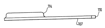
도 2를 참조하면, 안테나의 근위단에는 인쇄 회로 기판(107), 예를 들면 다층 인쇄 회로 기판(PCB)이 장착된다. 다층 회로 기판들은 통상적으로 다수의 절연 재료층을 사용한다. 상이한 재료들이 상이한 절연층들에 사용될 수 있다. 도전성 트랙들은 층들 사이에 인쇄 회로 기판의 외부층의 표면 위에 형성된다. 이러한 인쇄 회로 기판은 파선으로 나타낸 내측 도전체(108), 및 도 3 및 도 4에서 더 명확하게 알 수 있는 외측 차폐 도전체들(109A, 109B)을 가진다. 도 4는 PCB(107)에 장착된 안테나를 나타내는 안테나의 근위단의 도면이고, PCB는 도 2에 나타낸 선 AB 상에서 절단된다. 안테나의 근위단은 안테나 엘리먼트(element)들(102A, 102B, 102C, 102D) 각각에 각각 접속된 4개의 반경방향(radial) 엘리먼트(element)들(105A, 105B, 105C, 105D)을 가진다. 엘리먼트(element)들(106A, 106B)을 접속하여 2쌍의 원호를 형성하기 위해 반경방향(radial) 엘리먼트(element)들이 상호접속된다. 기판(107)은 안테나의 근위단을 가로질러 정반대에 위치된다. 안테나의 코어는 안테나를 제 위치에 유지하기 위해 기판의 탭(110)(도 2 참조)이 연장(extend)하는 근위단에 오목부(103R)를 가진다. 오목부(103R)는 도시된 것과 같이, 탭(110)의 길이에 대응하는 깊이의 폐쇄 오목부일 수 있고, 또는 그것은 코어(103)를 통해 연장(extend)할 수 있다. 기판과 안테나 사이의 연결부에서, 내측 도전체는 접속 엘리먼트(element)(106A)에 전기적으로 접속된다. 외측 도전체들(109A, 109B)은 모두 기판과 안테나 사이의 연결부에서 접속 엘리먼트(element)(106B)에 접속된다. 따라서, 기판의 내측 및 외측 도전체들은 루프 안테나(101)를 위한 전송 라인 피더를 형성한다.Referring to FIG. 2, a printed
도 2에서 알 수 있는 것과 같이, 기판(107)은 안테나와 실질적으로 동일한 폭의 사각형 다층 회로 기판이다. 내측 도전체(108)는 기판의 길이방향으로 배열된 길다란 트랙을 포함하고 또한 전송 라인을 안테나 및 수신 회로에 결합하는 데 적합한 내측 도전체의 각각의 단부(end)들에 있는 연장부들을 제외하고, 실질적으로 사각형이다. 내측 도전체(108)는 회로 기판(107)보다 좁고 그러므로 PCB의 절연층들은 내측 도전체의 양측 위에서 내측 도전체보다 더 멀리 연장(extend)한다. 외측 도전체들(109A, 109B)은 안테나와 수신 회로 사이의 사각형 회로 기판의 모두를 거 의 덮도록 배열된다. 따라서, 외측 도전체들은 또한 내측 도전체의 양측 위에서 내측 도전체보다 더 멀리 연장(extend)한다. 회로 기판은 안테나 시스템이 배치되는 디바이스의 일부를 형성하는 대형 회로 기판의 일부를 형성할 수 있다.As can be seen in FIG. 2, the
도 7을 참조하면, 복수의 비어(via)들(111)이 외측 도전체들 사이에 형성된다. 외측 도전체들은 절연성 회로 기판의 적어도 2개의 층들을 이들 사이에 배치한다. 비어는 그 내측 표면 위에 도전성 코팅을 가진 회로 기판에 형성되는 구멍(hole)이다. 그러므로, 그것은 회로 기판의 대향 표면들 위에서 도전체들을 전기적으로 연결한다. 도 7에서, 비어들은 회로 기판의 길이방향 에지들을 따라 형성되고, 여기서 외측 도전체들은 내측 도전체를 넘어 연장(extend)하는 것을 알 수 있다. 이러한 방식으로, 외측 도전체들은 외측 도전체들로부터 전기적으로 절연된 채로 있는, 내측 도전체에 대한 차폐물을 형성하기 위해 전기적으로 상호접속된다. 이러한 구성은 전송 라인이 방사 엘리먼트(radiating element)로서 작용하는 것을 방지한다. 안테나 코어 위에 도금된 도전체들만이 방사한다.Referring to FIG. 7, a plurality of
AB(도 2)에 대한 단면도인 도 3을 참조하면, 내측 도전체(108) 및 외측 도전체들(109A, 109B)이 다층 회로 기판(107)의 절연층들 사이에 개재된 도전성 트랙들로서 도시된다. 또한 외측 도전체들(109A, 109B)을 전기적으로 상호접속하는 비어들(111)이 도시된다.Referring to FIG. 3, which is a cross sectional view of AB (FIG. 2), the
도 2를 다시 참조하면, 내측 및 외측 도전체들은 스크린 또는 패러데이 상자(cage)(114) 내에 배치되는 적어도 하나의 증폭기(113)를 포함하는 수신 회로(112)에 결합된다. 스크린(114)은 도 5의 측면도에 나타난다. 외측 도전체들은 증폭기의 접지 터미널에 또한 전기적으로 접속되는 패러데이 상자에 전기적으로 접속된다. 내측 도전체는 패러데이 상자 내부에서 종단(terminate)하고 증폭기에 결합된다. 결과적으로, 접지에 대한 안테나의 접속만이 수신기 회로 입력에서 이들이 접지 접속 및 전송 라인 외측 도전체들(109A, 109B)에 의해 이루어진다. 안테나와 증폭기 사이에서 접지에 대한 다른 접속은 없다.Referring again to FIG. 2, the inner and outer conductors are coupled to a receiving
내측 도전체(108)는 비어(118)에 의해 수신 회로(112)에 전기적으로 연결되고, 외측 도전체들(109A, 109B)은, 도 6에서 알 수 있는 것과 같이, 비어(119)에 의해 수신 회로의 접지면에 전기적으로 연결된다. 안테나 근방의 인쇄 회로 기판의 단부(end)에서, 내측 도전체는 비어(120)에 의해 기판(107)의 외측 표면 위의 도전성 패드(pad)(122)에 전기적으로 접속되고, 외측 도전체는 도 2에서 알 수 있는 것과 같이, 비어(121)에 의해 외측 표면 위의 다른 도전성 패드(123)에 전기적으로 접속된다. 패드들(122, 123)은 안테나의 근위면 위에서 도전성 트랙들에 대한 접속을 허용한다.The
전류 쵸크는 수신 회로와 안테나 사이에 배치되어 안테나 신호들에 대한 공통-모드 노이즈의 중첩(superimposition)을 감소시키고 전송 라인 외측 도전체들이 주변 영역으로부터 전자기 방사를 수신하는 구조의 일부로서 작용하는 것을 방지한다. 전류 쵸크는 도 2에서 알 수 있는 것과 같이, 슬리브 바룬(115)의 형태이다. 도 6은 기판(107) 위에서 제 위치에 있는 슬리브 바룬(115)의 측단면도이다. 슬리브 바룬은 한 쌍의 도전 플레이트들(116A, 116B)을 포함하고, 플레이트들 각각은 전송 라인의 외측 도전층들(109A, 109B) 중 각각의 하나 위에 놓이고 에지에서 바 람직하게는 안테나로부터 가장 먼 에지에서, 각각의 외측 도전층(109A, 109B)에 접속된다. 바룬 플레이트들(116A, 116B)은 바람직하게는, 도 2 및 도 6에서 알 수 있는 것과 같이, 복수의 비어들(117)을 이용하여 외측 도전체들(109A, 109B)에 접속된다. 각각의 슬리브 바룬 플레이트(116A, 116B)와 전송 라인의 하부 외측 도전층 사이에는 유전층이 있다. 바람직한 실시예에서, 이 층은 PCB의 일부를 형성하고, 통상은 약 4의 상대 유전 상수(εr)를 가진 세라믹-포함 플라스틱(ceramic-loaded plastics) 재료로 구성된다. FR-4는 이와 같은 재료의 일 예이다. 그것의 상대 유전 상수는 4.7이다. 각각의 슬리브 바룬 플레이트의 전기 길이는 하부 도전층에 접속된 에지 및 대향 에지(opposite edge)로부터 플레이트(plate)의 범위에서, 안테나의 동작 주파수에서 1/4 파장이다. 1575MHz의 안테나 동작 주파수에서, FR-4 기판을 이용하는 슬리브 바룬의 길이는 대략 2 cm이다. 이 바룬은 이 기술 분야에서 숙련된 사람에게 친숙한 방식으로 동작한다. 슬리브 바룬과 안테나 사이에서 노출된 전송 라인의 어떤 부분은 방사할 것이다. 그러므로, 바룬은 도 2에서 알 수 있는 것과 같이 가능하게는 안테나에 가깝게 위치된다.A current choke is placed between the receiving circuit and the antenna to reduce the superimposition of common-mode noise for the antenna signals and to prevent conductors outside the transmission line from acting as part of the structure to receive electromagnetic radiation from the surrounding area. do. The current choke is in the form of a
이러한 구성은 몇 가지 이점을 갖는다. 첫째, 바룬은 외측 도전체들 위의 전류를 저지하므로, 어떤 공통-모드 노이즈 신호들(예컨대 안테나가 장착되는 장비의 다른 회로에 의해 발생되는)이 패러데이 상자로 흘러가 버리고 전송 라인으로 들어가는 것을 방지한다. 이러한 방식으로 바룬은 전송 라인을 공통-모드 노이즈 신호들로부터 차단한다. 바룬은 안테나에 대해 평형 부하(balanced load)를 제공한다. 더욱이, 바룬은 안테나만이 방사하도록 안테나를 절연한다. 또한, 시스템의 공진 주파수는 안테나와 수신 회로 사이에 링크의 노출된 도전체들을 갖는 안테나보다는 오히려, 안테나에 의해서만 결정된다. 이것은 방사 및 공진 도전체 길이들이 일치하여 효율이 개선된다는 것을 의미한다.This configuration has several advantages. First, the balun blocks the current on the outer conductors, thus preventing any common-mode noise signals (e.g., generated by other circuitry of the equipment on which the antenna is mounted) from flowing into the Faraday box and entering the transmission line. . In this way, balun shields the transmission line from common-mode noise signals. Barun provides a balanced load on the antenna. Moreover, the balun insulates the antenna so that only the antenna radiates. In addition, the resonant frequency of the system is determined only by the antenna, rather than an antenna with exposed conductors of the link between the antenna and the receiving circuit. This means that the radiated and resonant conductor lengths match and the efficiency is improved.
대안으로서, 전류 쵸크는 절반 바룬 슬리브(half barun sleeve)에 의해 형성될 수 있다. 이와 같은 구성에서, 단지 하나의 도전체, 예를 들면 116A가 사용된다. 이것은 실질적으로 완전한 바룬 슬리브(full barun sleeve)와 동일한 효과를 갖는다. 다른 대안은 강자성 전류 쵸크를 사용하는 것이다. 강자성 플레이트들은 슬리브 바룬과 유사한 방식으로 전송 라인의 양측 위에 배치된다. 이와 같은 구성의 이점은 플레이트들이 1/4 파장의 길이일 필요가 없어, 더 컴팩트한 디자인을 허용한다는 것이다. 쵸크는 또한 전송 라인과 연결된 동축 TEM 공진기로서 구현될 수 있고, 전송 라인은 바람직하게는 동축 라인의 형태일 수 있다. 이와 같은 공진기는 통상 1/4파 오픈-엔디드 절연체 충전 공동(quarter-wave open-ended dielectrically-loaded cavity)으로서 구현될 수 있다. As an alternative, the current choke can be formed by a half barun sleeve. In such a configuration, only one conductor is used, for example 116A. This has substantially the same effect as a full barun sleeve. Another alternative is to use ferromagnetic current chokes. Ferromagnetic plates are arranged on both sides of the transmission line in a manner similar to sleeve baluns. The advantage of this configuration is that the plates do not have to be a quarter wavelength long, allowing for a more compact design. The choke can also be implemented as a coaxial TEM resonator connected with a transmission line, which transmission line is preferably in the form of a coaxial line. Such a resonator may typically be implemented as a quarter-wave open-ended dielectrically-loaded cavity.
Claims (25)
Applications Claiming Priority (2)
| Application Number | Priority Date | Filing Date | Title |
|---|---|---|---|
| GB0609518A GB2437998B (en) | 2006-05-12 | 2006-05-12 | An antenna system |
| GB0609518.6 | 2006-05-12 |
Publications (1)
| Publication Number | Publication Date |
|---|---|
| KR20090013228A true KR20090013228A (en) | 2009-02-04 |
Family
ID=36637445
Family Applications (1)
| Application Number | Title | Priority Date | Filing Date |
|---|---|---|---|
| KR1020087029981A KR20090013228A (en) | 2006-05-12 | 2007-05-02 | An antenna system |
Country Status (7)
| Country | Link |
|---|---|
| US (1) | US7528796B2 (en) |
| JP (1) | JP2009537105A (en) |
| KR (1) | KR20090013228A (en) |
| CN (1) | CN101443955B (en) |
| GB (1) | GB2437998B (en) |
| TW (1) | TW200805781A (en) |
| WO (1) | WO2007132161A1 (en) |
Families Citing this family (16)
| Publication number | Priority date | Publication date | Assignee | Title |
|---|---|---|---|---|
| GB0623774D0 (en) | 2006-11-28 | 2007-01-10 | Sarantel Ltd | An Antenna Assembly Including a Dielectrically Loaded Antenna |
| BRPI1009330A2 (en) | 2009-03-12 | 2016-03-08 | Sarantel Ltd | dielectrically charged antenna |
| GB0911635D0 (en) | 2009-07-03 | 2009-08-12 | Sarantel Ltd | A dielectrically-loaded antenna |
| US8456375B2 (en) | 2009-05-05 | 2013-06-04 | Sarantel Limited | Multifilar antenna |
| US8514144B2 (en) * | 2009-07-30 | 2013-08-20 | Jim D. Gray & Associates, Inc. | Antenna system and connector for antenna |
| US8599101B2 (en) | 2010-01-27 | 2013-12-03 | Sarantel Limited | Dielectrically loaded antenna and radio communication apparatus |
| GB2477290B (en) * | 2010-01-27 | 2014-04-09 | Harris Corp | A dielectrically loaded antenna and radio communication apparatus |
| GB2477289B (en) * | 2010-01-27 | 2014-08-13 | Harris Corp | A radio communication apparatus having improved resistance to common mode noise |
| CN103327808B (en) * | 2010-11-08 | 2015-05-06 | Pandeb控股有限公司 | An irrigation system |
| CN102394384B (en) * | 2011-07-19 | 2014-12-10 | 惠州Tcl移动通信有限公司 | Mobile equipment, mobile phone and antenna structure thereof |
| US10135134B2 (en) * | 2012-06-21 | 2018-11-20 | Richwave Technology Corp. | Antenna system for receiving and transmitting wireless signals |
| DE102014114164A1 (en) * | 2014-09-30 | 2016-03-31 | Rational Ag | Antenna for detecting microwave radiation and cooking appliance |
| CN106329073B (en) * | 2016-08-24 | 2019-10-01 | 西安电子科技大学 | A kind of sensor antenna |
| JP6614109B2 (en) * | 2016-11-21 | 2019-12-04 | 株式会社村田製作所 | Electronic equipment with wireless circuit |
| CN107027079B (en) * | 2017-05-12 | 2024-02-27 | 深圳市冠旭电子股份有限公司 | Necklace type Bluetooth earphone |
| EP3537535B1 (en) * | 2018-03-07 | 2022-05-11 | Nokia Shanghai Bell Co., Ltd. | Antenna assembly |
Family Cites Families (67)
| Publication number | Priority date | Publication date | Assignee | Title |
|---|---|---|---|---|
| GB587627A (en) * | 1944-09-09 | 1947-05-01 | Donald Jackson | Improvements in or relating to radio receiving devices |
| US3599220A (en) * | 1968-10-24 | 1971-08-10 | Itt | Conical spiral loop antenna |
| US4008479A (en) * | 1975-11-03 | 1977-02-15 | Chu Associates, Inc. | Dual-frequency circularly polarized spiral antenna for satellite navigation |
| US4114164A (en) * | 1976-12-17 | 1978-09-12 | Transco Products, Inc. | Broadband spiral antenna |
| US4554554A (en) * | 1983-09-02 | 1985-11-19 | The United States Of America As Represented By The Secretary Of The Navy | Quadrifilar helix antenna tuning using pin diodes |
| US4608574A (en) * | 1984-05-16 | 1986-08-26 | The United States Of America As Represented By The Secretary Of The Air Force | Backfire bifilar helix antenna |
| US4658262A (en) * | 1985-02-19 | 1987-04-14 | Duhamel Raymond H | Dual polarized sinuous antennas |
| GB8707231D0 (en) | 1987-03-26 | 1987-04-29 | Analytical Instr Ltd | Temperature compensation in pressure leak detection |
| JPH0834374B2 (en) * | 1989-04-19 | 1996-03-29 | 松下電器産業株式会社 | Wireless antenna device |
| GB2246910B (en) | 1990-08-02 | 1994-12-14 | Polytechnic Electronics Plc | A radio frequency antenna |
| JPH04113705A (en) * | 1990-09-03 | 1992-04-15 | Matsushita Electric Ind Co Ltd | Microwave multi-stage amplifier |
| US5346300A (en) * | 1991-07-05 | 1994-09-13 | Sharp Kabushiki Kaisha | Back fire helical antenna |
| JP2719856B2 (en) * | 1991-07-05 | 1998-02-25 | シャープ株式会社 | Backfire helical antenna |
| JPH0548320A (en) | 1991-08-20 | 1993-02-26 | Sumitomo Electric Ind Ltd | Receiver |
| US5349365A (en) * | 1991-10-21 | 1994-09-20 | Ow Steven G | Quadrifilar helix antenna |
| US5708445A (en) | 1993-01-29 | 1998-01-13 | Motorola, Inc. | Antenna assembly for radio circuit and method therefor |
| US5440317A (en) * | 1993-05-17 | 1995-08-08 | At&T Corp. | Antenna assembly for a portable transceiver |
| US5594461A (en) * | 1993-09-24 | 1997-01-14 | Rockwell International Corp. | Low loss quadrature matching network for quadrifilar helix antenna |
| US6011524A (en) * | 1994-05-24 | 2000-01-04 | Trimble Navigation Limited | Integrated antenna system |
| GB2292257B (en) | 1994-06-22 | 1999-04-07 | Sidney John Branson | An antenna |
| GB9417450D0 (en) | 1994-08-25 | 1994-10-19 | Symmetricom Inc | An antenna |
| US5559521A (en) * | 1994-12-08 | 1996-09-24 | Lucent Technologies Inc. | Antennas with means for blocking current in ground planes |
| US5635945A (en) * | 1995-05-12 | 1997-06-03 | Magellan Corporation | Quadrifilar helix antenna |
| JPH09153725A (en) * | 1995-11-30 | 1997-06-10 | Advantest Corp | Probe antenna |
| GB9601250D0 (en) * | 1996-01-23 | 1996-03-27 | Symmetricom Inc | An antenna |
| GB9603914D0 (en) * | 1996-02-23 | 1996-04-24 | Symmetricom Inc | An antenna |
| US5838282A (en) * | 1996-03-22 | 1998-11-17 | Ball Aerospace And Technologies Corp. | Multi-frequency antenna |
| GB9606593D0 (en) | 1996-03-29 | 1996-06-05 | Symmetricom Inc | An antenna system |
| US5706019A (en) * | 1996-06-19 | 1998-01-06 | Motorola, Inc. | Integral antenna assembly for a radio and method of manufacturing |
| KR100199016B1 (en) * | 1996-12-02 | 1999-06-15 | 정선종 | Satellite tracking method for vehicle-mounted antenna systems |
| JP3580654B2 (en) * | 1996-12-04 | 2004-10-27 | 京セラ株式会社 | Common antenna and portable radio using the same |
| JPH11239020A (en) * | 1997-04-18 | 1999-08-31 | Murata Mfg Co Ltd | Circular polarizing antenna and radio device using same |
| US6031495A (en) * | 1997-07-02 | 2000-02-29 | Centurion Intl., Inc. | Antenna system for reducing specific absorption rates |
| US6384798B1 (en) * | 1997-09-24 | 2002-05-07 | Magellan Corporation | Quadrifilar antenna |
| US6094178A (en) * | 1997-11-14 | 2000-07-25 | Ericsson, Inc. | Dual mode quadrifilar helix antenna and associated methods of operation |
| FI113814B (en) * | 1997-11-27 | 2004-06-15 | Nokia Corp | Multifunctional helix antennas |
| US6167039A (en) | 1997-12-17 | 2000-12-26 | Telefonaktiebolget Lm Ericsson | Mobile station having plural antenna elements and interference suppression |
| GB9813002D0 (en) * | 1998-06-16 | 1998-08-12 | Symmetricom Inc | An antenna |
| US6133891A (en) * | 1998-10-13 | 2000-10-17 | The United States Of America As Represented By The Secretary Of The Navy | Quadrifilar helix antenna |
| GB9828768D0 (en) * | 1998-12-29 | 1999-02-17 | Symmetricom Inc | An antenna |
| GB9902765D0 (en) * | 1999-02-08 | 1999-03-31 | Symmetricom Inc | An antenna |
| GB9912441D0 (en) | 1999-05-27 | 1999-07-28 | Symmetricon Inc | An antenna |
| JP3399513B2 (en) | 1999-08-10 | 2003-04-21 | 日本電気株式会社 | Helical antenna and manufacturing method thereof |
| GB2356086B (en) * | 1999-11-05 | 2003-11-05 | Symmetricom Inc | Antenna manufacture |
| US6229499B1 (en) * | 1999-11-05 | 2001-05-08 | Xm Satellite Radio, Inc. | Folded helix antenna design |
| US6765541B1 (en) * | 2000-04-24 | 2004-07-20 | The United States Of America As Represented By The Secretary Of The Navy | Capacitatively shunted quadrifilar helix antenna |
| US6229488B1 (en) * | 2000-09-08 | 2001-05-08 | Emtac Technology Corp. | Antenna for receiving signals from GPS and GSM |
| US6727781B2 (en) * | 2000-09-18 | 2004-04-27 | Daido Steel Co., Ltd. | High frequency amplifier |
| US6476776B1 (en) * | 2000-11-14 | 2002-11-05 | Motorola, Inc. | Satellite adaptive antenna system |
| US6480173B1 (en) * | 2000-11-28 | 2002-11-12 | Receptec Llc | Quadrifilar helix feed network |
| US20020113731A1 (en) * | 2001-02-22 | 2002-08-22 | Strickland Peter C. | Satellite communciation antenna array |
| JP3574420B2 (en) * | 2001-06-05 | 2004-10-06 | 三星電子株式会社 | Portable terminal |
| JP3905334B2 (en) * | 2001-07-25 | 2007-04-18 | シャープ株式会社 | Receiver |
| US6897825B2 (en) | 2001-10-29 | 2005-05-24 | Samsung Electronics Co., Ltd. | Antenna apparatus for folder type mobile phone |
| WO2003044895A1 (en) * | 2001-11-23 | 2003-05-30 | Navman Nz Limited | Quadrifilar helical antenna and feed network |
| DE10208164B4 (en) * | 2002-02-26 | 2006-01-12 | Advanced Micro Devices, Inc., Sunnyvale | Method for controlling an electrical property of a field effect transistor |
| GB0505771D0 (en) | 2005-03-21 | 2005-04-27 | Sarantel Ltd | Dielectrically-loaded antenna |
| GB2399948B (en) * | 2003-03-28 | 2006-06-21 | Sarantel Ltd | A dielectrically-loaded antenna |
| DE10323244A1 (en) * | 2003-05-22 | 2004-12-16 | Infineon Technologies Ag | Integrated memory circuit arrangement, in particular UCP flash memory |
| TWI238566B (en) | 2004-07-30 | 2005-08-21 | Inpaq Technology Co Ltd | Manufacture method of a multi-operating frequency antenna and the device thereof |
| DE102004040258A1 (en) * | 2004-08-18 | 2006-02-23 | I-Peng Feng | Cylindrical metallized-ceramic antenna for receiving circularly-polarized waves, e.g. from GPS satellites, includes printed metallized antenna elements, balun and matching circuitry |
| US7002530B1 (en) * | 2004-09-30 | 2006-02-21 | Etop Technology Co., Ltd. | Antenna |
| GB0422179D0 (en) * | 2004-10-06 | 2004-11-03 | Sarantel Ltd | Antenna feed structure |
| TWI248230B (en) | 2004-11-25 | 2006-01-21 | Htc Corp | Method for manufacturing a helix antenna |
| TW200713693A (en) | 2005-06-21 | 2007-04-01 | Sarantel Ltd | An antenna and an antenna feed structure |
| GB2430556B (en) * | 2005-09-22 | 2009-04-08 | Sarantel Ltd | A mobile communication device and an antenna assembly for the device |
| CN2899134Y (en) | 2005-11-11 | 2007-05-09 | 哗裕实业股份有限公司 | Antenna feeding structural improvement |
-
2006
- 2006-05-12 GB GB0609518A patent/GB2437998B/en not_active Expired - Fee Related
-
2007
- 2007-05-02 CN CN2007800170922A patent/CN101443955B/en not_active Expired - Fee Related
- 2007-05-02 KR KR1020087029981A patent/KR20090013228A/en not_active Application Discontinuation
- 2007-05-02 WO PCT/GB2007/001612 patent/WO2007132161A1/en active Application Filing
- 2007-05-02 JP JP2009510523A patent/JP2009537105A/en active Pending
- 2007-05-07 TW TW096116100A patent/TW200805781A/en unknown
- 2007-05-10 US US11/803,405 patent/US7528796B2/en not_active Expired - Fee Related
Also Published As
| Publication number | Publication date |
|---|---|
| CN101443955A (en) | 2009-05-27 |
| US20080036689A1 (en) | 2008-02-14 |
| GB2437998B (en) | 2009-11-11 |
| GB0609518D0 (en) | 2006-06-21 |
| JP2009537105A (en) | 2009-10-22 |
| TW200805781A (en) | 2008-01-16 |
| US7528796B2 (en) | 2009-05-05 |
| CN101443955B (en) | 2013-05-22 |
| GB2437998A (en) | 2007-11-14 |
| WO2007132161A1 (en) | 2007-11-22 |
Similar Documents
| Publication | Publication Date | Title |
|---|---|---|
| KR20090013228A (en) | An antenna system | |
| US9865928B2 (en) | Dual-polarized antenna | |
| KR101333675B1 (en) | A mobile communication device and an antenna assembly for the device | |
| US4475108A (en) | Electronically tunable microstrip antenna | |
| US6903687B1 (en) | Feed structure for antennas | |
| US6690336B1 (en) | Antenna | |
| US7688265B2 (en) | Dual polarized low profile antenna | |
| US7903044B2 (en) | Dielectrically-loaded antenna | |
| US5444452A (en) | Dual frequency antenna | |
| TWI233711B (en) | Low profile, dual polarized/pattern antenna | |
| US8134506B2 (en) | Antenna arrangement | |
| WO2011016045A2 (en) | Printed quasi-tapered tape helical array antenna | |
| JPH0259642B2 (en) | ||
| US20120299798A1 (en) | Dielectrically Loaded Antenna | |
| JP3996879B2 (en) | Coupling structure of dielectric waveguide and microstrip line, and filter substrate having this coupling structure | |
| JP2001044753A (en) | Integrated radiator tile with low profile for dual linearly and circularly polarized broadband phased array | |
| KR20190010991A (en) | Antenna | |
| JP6808103B2 (en) | Antenna device and communication device | |
| JP6590936B2 (en) | Coaxial horn excitation method for wide bandwidth and circular polarization | |
| JPH02156707A (en) | Planer antenna | |
| JP2000269708A (en) | Electromagnetic field coupling structure and electric circuit device using the same | |
| JP2002076724A (en) | Waveguide-flat cable converter | |
| JP2006067403A (en) | Stacked aperture antenna |
Legal Events
| Date | Code | Title | Description |
|---|---|---|---|
| A201 | Request for examination | ||
| E902 | Notification of reason for refusal | ||
| E601 | Decision to refuse application |