KR20090013027A - Display device and method of driving the same - Google Patents
Display device and method of driving the same Download PDFInfo
- Publication number
- KR20090013027A KR20090013027A KR1020080063339A KR20080063339A KR20090013027A KR 20090013027 A KR20090013027 A KR 20090013027A KR 1020080063339 A KR1020080063339 A KR 1020080063339A KR 20080063339 A KR20080063339 A KR 20080063339A KR 20090013027 A KR20090013027 A KR 20090013027A
- Authority
- KR
- South Korea
- Prior art keywords
- signal level
- transistor
- signal
- driving
- period
- Prior art date
Links
Images


Classifications
-
- G—PHYSICS
- G09—EDUCATION; CRYPTOGRAPHY; DISPLAY; ADVERTISING; SEALS
- G09G—ARRANGEMENTS OR CIRCUITS FOR CONTROL OF INDICATING DEVICES USING STATIC MEANS TO PRESENT VARIABLE INFORMATION
- G09G3/00—Control arrangements or circuits, of interest only in connection with visual indicators other than cathode-ray tubes
- G09G3/20—Control arrangements or circuits, of interest only in connection with visual indicators other than cathode-ray tubes for presentation of an assembly of a number of characters, e.g. a page, by composing the assembly by combination of individual elements arranged in a matrix no fixed position being assigned to or needed to be assigned to the individual characters or partial characters
- G09G3/22—Control arrangements or circuits, of interest only in connection with visual indicators other than cathode-ray tubes for presentation of an assembly of a number of characters, e.g. a page, by composing the assembly by combination of individual elements arranged in a matrix no fixed position being assigned to or needed to be assigned to the individual characters or partial characters using controlled light sources
- G09G3/30—Control arrangements or circuits, of interest only in connection with visual indicators other than cathode-ray tubes for presentation of an assembly of a number of characters, e.g. a page, by composing the assembly by combination of individual elements arranged in a matrix no fixed position being assigned to or needed to be assigned to the individual characters or partial characters using controlled light sources using electroluminescent panels
- G09G3/32—Control arrangements or circuits, of interest only in connection with visual indicators other than cathode-ray tubes for presentation of an assembly of a number of characters, e.g. a page, by composing the assembly by combination of individual elements arranged in a matrix no fixed position being assigned to or needed to be assigned to the individual characters or partial characters using controlled light sources using electroluminescent panels semiconductive, e.g. using light-emitting diodes [LED]
- G09G3/3208—Control arrangements or circuits, of interest only in connection with visual indicators other than cathode-ray tubes for presentation of an assembly of a number of characters, e.g. a page, by composing the assembly by combination of individual elements arranged in a matrix no fixed position being assigned to or needed to be assigned to the individual characters or partial characters using controlled light sources using electroluminescent panels semiconductive, e.g. using light-emitting diodes [LED] organic, e.g. using organic light-emitting diodes [OLED]
- G09G3/3225—Control arrangements or circuits, of interest only in connection with visual indicators other than cathode-ray tubes for presentation of an assembly of a number of characters, e.g. a page, by composing the assembly by combination of individual elements arranged in a matrix no fixed position being assigned to or needed to be assigned to the individual characters or partial characters using controlled light sources using electroluminescent panels semiconductive, e.g. using light-emitting diodes [LED] organic, e.g. using organic light-emitting diodes [OLED] using an active matrix
- G09G3/3233—Control arrangements or circuits, of interest only in connection with visual indicators other than cathode-ray tubes for presentation of an assembly of a number of characters, e.g. a page, by composing the assembly by combination of individual elements arranged in a matrix no fixed position being assigned to or needed to be assigned to the individual characters or partial characters using controlled light sources using electroluminescent panels semiconductive, e.g. using light-emitting diodes [LED] organic, e.g. using organic light-emitting diodes [OLED] using an active matrix with pixel circuitry controlling the current through the light-emitting element
-
- H—ELECTRICITY
- H10—SEMICONDUCTOR DEVICES; ELECTRIC SOLID-STATE DEVICES NOT OTHERWISE PROVIDED FOR
- H10K—ORGANIC ELECTRIC SOLID-STATE DEVICES
- H10K59/00—Integrated devices, or assemblies of multiple devices, comprising at least one organic light-emitting element covered by group H10K50/00
- H10K59/10—OLED displays
-
- G—PHYSICS
- G09—EDUCATION; CRYPTOGRAPHY; DISPLAY; ADVERTISING; SEALS
- G09G—ARRANGEMENTS OR CIRCUITS FOR CONTROL OF INDICATING DEVICES USING STATIC MEANS TO PRESENT VARIABLE INFORMATION
- G09G2300/00—Aspects of the constitution of display devices
- G09G2300/08—Active matrix structure, i.e. with use of active elements, inclusive of non-linear two terminal elements, in the pixels together with light emitting or modulating elements
- G09G2300/0809—Several active elements per pixel in active matrix panels
- G09G2300/0819—Several active elements per pixel in active matrix panels used for counteracting undesired variations, e.g. feedback or autozeroing
-
- G—PHYSICS
- G09—EDUCATION; CRYPTOGRAPHY; DISPLAY; ADVERTISING; SEALS
- G09G—ARRANGEMENTS OR CIRCUITS FOR CONTROL OF INDICATING DEVICES USING STATIC MEANS TO PRESENT VARIABLE INFORMATION
- G09G2300/00—Aspects of the constitution of display devices
- G09G2300/08—Active matrix structure, i.e. with use of active elements, inclusive of non-linear two terminal elements, in the pixels together with light emitting or modulating elements
- G09G2300/0809—Several active elements per pixel in active matrix panels
- G09G2300/0842—Several active elements per pixel in active matrix panels forming a memory circuit, e.g. a dynamic memory with one capacitor
- G09G2300/0861—Several active elements per pixel in active matrix panels forming a memory circuit, e.g. a dynamic memory with one capacitor with additional control of the display period without amending the charge stored in a pixel memory, e.g. by means of additional select electrodes
- G09G2300/0866—Several active elements per pixel in active matrix panels forming a memory circuit, e.g. a dynamic memory with one capacitor with additional control of the display period without amending the charge stored in a pixel memory, e.g. by means of additional select electrodes by means of changes in the pixel supply voltage
-
- G—PHYSICS
- G09—EDUCATION; CRYPTOGRAPHY; DISPLAY; ADVERTISING; SEALS
- G09G—ARRANGEMENTS OR CIRCUITS FOR CONTROL OF INDICATING DEVICES USING STATIC MEANS TO PRESENT VARIABLE INFORMATION
- G09G2320/00—Control of display operating conditions
- G09G2320/04—Maintaining the quality of display appearance
- G09G2320/043—Preventing or counteracting the effects of ageing
-
- H—ELECTRICITY
- H01—ELECTRIC ELEMENTS
- H01L—SEMICONDUCTOR DEVICES NOT COVERED BY CLASS H10
- H01L2924/00—Indexing scheme for arrangements or methods for connecting or disconnecting semiconductor or solid-state bodies as covered by H01L24/00
- H01L2924/10—Details of semiconductor or other solid state devices to be connected
- H01L2924/11—Device type
- H01L2924/12—Passive devices, e.g. 2 terminal devices
- H01L2924/1204—Optical Diode
- H01L2924/12044—OLED
Abstract
Description
본 발명은 2007년 7월 30일에 일본 특허청에 출원된 일본 특허 JP 2007-197081에 관한 주제를 포함하며, 그 모든 내용은 여기에 참조에 의해 포함된다.The present invention includes the subject matter related to Japanese Patent JP 2007-197081, filed with the Japan Patent Office on July 30, 2007, the entire contents of which are incorporated herein by reference.
본 발명은 표시장치 및 그 구동방법에 관한 것으로, 예를 들면 폴리실리콘 TFT(Thin Film Transistor)를 사용한 유기EL(Electro Luminescence)소자로 구성된 화소를 가진 액티브 매트릭스형 디스플레이 장치에 적용할 수 있다. 본 발명은 발광소자의 발광을 정지시키는 비발광 기간 내에 있어서의, 발광소자의 구동에 아무런 영향을 주지 않는 기간의 전부 기간 또는 일부 기간 동안의 기록신호의 신호레벨을, 상기 전부 기간 또는 상기 일부 기간을 제외한 다른 기간에 있어서 기간이 짧은 측의 상기 기록신호의 신호레벨로 설정함으로써, 시간에 따른 변화에 의한 화질의 열화, 계조를 설정할 수 없게 되는 현상을 효과적으로 회피할 수 있도록 한다.BACKGROUND OF THE
종래, 유기EL소자를 사용한 디스플레이 장치에 관해서 여러 가지 기술이 제안되었다. 이들 여러 가지 기술은 예를 들면 USP 5,684,365, 일본국 공개특허 공보 특개 평8-234683호에 기재되어 있다.Conventionally, various techniques have been proposed regarding a display device using an organic EL element. These various techniques are described, for example in WPS 5,684,365 and Unexamined-Japanese-Patent No. 8-234683.
여기에서 도 2는, 종래의 유기EL소자를 사용한 소위 액티브 매트릭스형 디스플레이 장치를 나타내는 블럭도다. 디스플레이 장치(1)에 있어서, 표시부(2)는, 매트릭스 모양으로 화소(3)가 배치되어서 형성된다. 또 표시부(2)에는, 매트릭스 모양으로 배치한 화소(3)에 대하여, 주사선 SCN이 라인 단위로 수평방향으로 설치되고, 주사선 SCN과 직교하도록 신호선 SIG이 열마다 설치된다.2 is a block diagram showing a so-called active matrix display device using a conventional organic EL element. In the
여기에서 도 3에 나타낸 바와 같이, 각 화소(3)는 전류구동형 자발광 소자인 유기EL소자(8)와, 이 유기EL소자(8)를 구동하는 각 화소(3)의 구동회로(이하, 화소회로라고 부른다)로 구성된다.As shown in FIG. 3, each
화소(3)에서는, 신호레벨 유지용 콘덴서 C1의 일단이 일정 전위로 유지되고, 기록신호 WS에 의해 온 오프 동작하는 트랜지스터 TR1을 통해, 이 신호레벨 유지용 콘덴서 C1의 타단이 신호선 SIG에 접속된다. 이에 따라 화소(3)에서는, 기록신호 WS의 상승에 의해 트랜지스터 TR1이 온 동작하고, 신호레벨 유지용 콘덴서 C1의 타단 전위가 신호선 SIG의 신호레벨로 설정된다. 또한 트랜지스터 TR1이 온 상태에서 오프 상태로 전환되는 타이밍에서, 신호선 SIG의 신호레벨이 신호레벨 유지용 콘덴서 C1의 타단에 샘플 홀드 된다.In the
화소(3)에서는, 소스를 전원 Vcc에 접속한 P채널형 트랜지스터 TR2의 게이트에, 이 신호레벨 유지용 콘덴서 C1의 타단이 접속되고, 이 트랜지스터 TR2의 드레인이 유기EL소자(8)의 애노드에 접속된다. 여기에서 화소(3)는 이 트랜지스터 TR2가 항상 포화 영역에서 동작하도록 설정된다. 그 결과, 트랜지스터 TR 2는, 다음 식 (1)로 나타내는 드레인 소스 전류 Ids에 의한 정전류회로를 구성한다.In the

여기에서 Vgs는 트랜지스터 TR2의 게이트 소스간 전압이며, μ는 이동도, W는 채널 폭, L은 채널 길이, Cox는 단위면적당 게이트 절연막의 용량, Vth는 트랜지스터 TR2의 임계값전압이다. 이에 따라 각 화소(3)는, 신호레벨 유지용 콘덴서 C1에 샘플 홀드 된 신호선 SIG의 신호레벨에 따른 구동전류 Ids(드레인 소스 전류)에 의해 유기EL소자(8)를 구동한다.Is the voltage between the gate and source of the transistor Tr2, μ is the mobility, W is the channel width, L is the channel length, C is the capacitance of the gate insulating film per unit area, and Pt is the threshold voltage of the transistor Tr2. As a result, each
디스플레이 장치(1)는, 수직구동회로(4)의 라이트 스캔 회로(WSCN)(4A)에 의해, 소정의 샘플링 펄스를 순차 전송하여, 각 화소(3)에의 기록을 지시하는 타이밍 신호인 기록신호 WS를 생성한다. 또 수평구동회로(5)의 수평 셀렉터(HSEL)(5A)에 의해, 소정의 샘플링 펄스를 순차 전송해서 타이밍 신호를 생성한다. 또한 타이밍 신호를 기준으로 해서 각 신호선 SIG를 입력 신호 S1의 신호레벨로 설정한다. 이에 따라 디스플레이 장치(1)는 점 순차 또는 선 순차로, 표시부(2)에 설치된 신호레벨 유지용 콘덴서 C1의 단자전압을 입력 신호 S1에 따라 설정하여, 입력 신호 S1에 의한 화상을 표시한다.The
여기에서 유기EL소자(8)는, 도 4에 나타낸 바와 같이, 장기간의 사용에 의해 전류가 흐르기 어려워지는 방향으로 전류전압특성이 경시 변화한다. 이때 도 4에 있어서, 부호 L1이 초기의 특성을 나타내고, 부호 L2가 시간에 따른 변화에 의 한 특성을 나타내는 것이다. 그러나 도 3에 나타내는 회로 구성에 의해 P채널형 트랜지스터 TR2로 유기EL소자(8)를 구동할 경우에는, 신호선 SIG의 신호레벨에 따라 설정된 게이트 소스간 전압 Vgs에 의해 트랜지스터 TR2가 유기EL소자(8)를 구동함으로써, 전류전압특성의 시간에 따른 변화에 의한 각 화소의 휘도 변화를 방지할 수 있다.In the
그런데 화소회로, 수평구동회로, 수직구동회로를 구성하는 트랜지스터를 모두 N채널형 트랜지스터로 구성하면, 아모포스 실리콘 프로세스로 이들 회로를 함께 유리 기판 등의 절연 기판 위에 제조할 수 있다. 그 결과 디스플레이 장치를 간이하게 제조할 수 있다.However, if the transistors constituting the pixel circuit, the horizontal drive circuit, and the vertical drive circuit are all composed of N-channel transistors, these circuits can be manufactured together on an insulating substrate such as a glass substrate by an amorphous silicon process. As a result, the display device can be manufactured simply.
그러나 도 3과의 대비로서 도 5에 나타낸 바와 같이, 트랜지스터 TR2에 N채널형을 적용해서 각 화소(13)를 형성하고, 이 화소(13)에 의한 표시부(12)로 디스플레이 장치(11)를 구성했을 경우, 트랜지스터 TR2의 소스가 유기EL소자(8)에 접속됨으로써, 도 4에 나타내는 전류전압특성의 변화에 의해, 트랜지스터 TR2의 게이트 소스간 전압 Vgs가 변화하게 된다. 이것에 의해 이 경우, 장시간의 사용에 의해 유기EL소자(8)에 흐르는 전류가 서서히 감소하여, 유기EL소자(8)의 발광 휘도가 서서히 저하하게 된다. 또한 도 5에 나타내는 구성에서는, 트랜지스터 TR2의 특성의 편차에 의해 화소마다 발광 휘도가 변동하게 된다. 이때 이 발광 휘도의 편차는, 표시 화면에 있어서의 균일성을 방해하고, 표시 화면의 불균일, 거칠기로 지각된다.However, in contrast to FIG. 3, as shown in FIG. 5, each
이 때문에 이러한 유기EL소자의 시간에 따른 변화에 의한 발광 휘도의 저 하, 특성의 편차에 의한 발광 휘도의 편차를 방지하는 기술로서, 예를 들면 도 6에 나타낸 바와 같이 각 화소를 구성하는 것을 생각해 볼 수 있다.For this reason, as a technique of preventing the fall of the light emission luminance due to the change with time of such an organic EL element and the deviation of the light emission luminance due to the variation of a characteristic, it is considered that each pixel is comprised, for example as shown in FIG. can see.
여기에서 도 6에 나타내는 디스플레이 장치(21)에 있어서, 표시부(22)는, 화소(23)를 매트릭스 모양으로 배치해서 형성된다. 화소(23)에서는, 신호레벨 유지용 콘덴서 C1의 일단이 유기EL소자(8)의 애노드에 접속된다. 또한 기록신호 WS에 따라 온 오프 동작하는 트랜지스터 TR1을 통해, 이 신호레벨 유지용 콘덴서 C1의 타단이 신호선 SIG에 접속된다. 이에 따라 화소(23)에서는, 기록신호 WS에 따라 신호레벨 유지용 콘덴서 C1의 타단의 전압이, 신호선 SIG의 신호레벨로 설정된다.Here, in the
화소(23)에서는, 이 신호레벨 유지용 콘덴서 C1의 양단이 트랜지스터 TR2의 소스 및 게이트에 접속된다. 또한 트랜지스터 TR2의 드레인이 전원공급용 주사선 SCN에 접속된다. 이에 따라 화소(23)는, 게이트 전압이 신호선 SIG의 신호레벨로 설정된 소스 폴로워 회로 구성의 트랜지스터 TR2에 의해 유기EL소자(8)를 구동한다. 또한 여기에서 Vcat는, 유기EL소자(8)의 캐소드 전위다.In the
디스플레이 장치(21)는, 수직구동회로(24)의 라이트 스캔 회로(WSCN)(24A), 드라이브 스캔 회로(DSCN)(24B)에 의해 주사선 SCN에 기록신호 WS, 전원용 구동신호 DS를 출력한다. 또 수평구동회로(25)의 수평 셀렉터(HSEL)(25A)에 의해 신호선 SIG에 구동신호 Ssig를 출력한다. 이에 따라 화소(23)의 동작을 제어한다.The
여기에서 도 7a 내지 7e는, 이 화소(23)의 동작을 나타내는 타임 차트다. 화 소(23)에서는, 유기EL소자(8)를 발광시키는 기간인 발광 기간 동안, 도 8에 나타낸 바와 같이 기록신호 WS에 의해 트랜지스터 TR1이 오프 상태로 설정되고, 구동신호 DS에 의해 트랜지스터 TR2에 전원전압 Vcc가 공급된다(도 7a 및 7b). 이에 따라 트랜지스터 TR2의 게이트 전압 Vg 및 소스 전압 Vs(도 7d 및 7e)가 신호레벨 유지용 콘덴서 C1의 양단 전압에 유지된다. 이로써 게이트 전압 Vg 및 소스 전압 Vs에 의한 구동전류 Ids로 유기EL소자(8)를 구동한다. 이때 구동전류 Ids는 식 (1)로 나타낸다.7A to 7E are time charts showing the operation of the
화소(23)에서는, 발광 기간이 종료되면, 도 9에 나타낸 바와 같이 구동신호 DS에 의해 트랜지스터 TR2의 드레인 전압이 소정 전압 Vss로 하강한다. 여기에서 소정 전압 Vss는 유기EL소자(8)의 임계값전압 Vth에 유기EL소자(8)의 캐소드 전압 Vcat를 가산한 전압보다 낮은 전압으로 설정된다. 이에 따라 구동용 트랜지스터 TR2의 구동신호 DS측이 소스로서 기능하고, 유기EL소자(8)의 애노드 전압(도 7e에서는 전압 Vs)이 상승하여, 유기EL소자(8)가 발광을 정지한다.In the
이 때 화소(23)에서는, 도 9에 있어서 화살표로 나타낸 바와 같이, 신호레벨 유지용 콘덴서 C1의 유기EL소자(8) 측으로부터 축적 전하가 방전하고, 이에 따라 유기EL소자(8)의 애노드 전압이 하강하여 전압 Vss로 설정된다.At this time, in the
이어서 화소(23)에서는, 도 10에 나타낸 바와 같이, 구동신호 Ssig에 의해 신호선 SIG가 소정 전압 Vofs로 하강하고, 기록신호 WS에 의해 트랜지스터 TR1이 오프 상태에서 온 상태로 전환된다(도 7a 및 7c). 이에 따라 화 소(23)에서는, 트랜지스터 TR2의 게이트 전압 Vg가 이 신호선 SIG의 전압 Vofs로 설정되고, 트랜지스터 TR2의 게이트 소스간 전압 Vgs가, Vofs-Vss로 설정된다. 여기에서 트랜지스터 TR2의 임계값전압을 Vth라고 하면, 전압 Vofs는, 트랜지스터 TR2의 게이트 소스간 전압 Vgs가 트랜지스터 TR2의 임계값전압 Vth보다 커지도록 설정된다.Next, in the
이어서 도 7a 내지 7e에 있어서 부호 Tth1로 나타내는 기간 동안, 트랜지스터 TR1을 온 상태로 유지한 상태에서, 구동신호 DS에 의해 트랜지스터 TR2의 드레인 전압이 전원전압 Vcc로 하강한다. 이에 따라 화소(23)에서는, 도 11에 있어서 화살표로 나타낸 바와 같이, 신호레벨 유지용 콘덴서 C1의 단자간 전압이 트랜지스터 TR2의 임계값전압보다 클 경우, 전원 Vcc로부터 신호레벨 유지용 콘덴서 C1의 유기EL소자(8)측단에 충전 전류가 흘러, 유기EL소자(8)측단의 전압 Vs가 서서히 상승한다. 여기에서 유기EL소자(8)는, 다이오드와 용량 Cel의 병렬회로로 등가회로가 표현된다. 여기에서 도 11에 나타내는 상태에서는, 트랜지스터 TR2를 통해 전원 Vcc로부터 유기EL소자(8)에도 전류가 유입된다. 그러나 트랜지스터 TR2의 소스 전압의 상승에 의해 유기EL소자(8)의 단자간 전압이 유기EL소자(8)의 임계값전압을 초과하지 않는 한, 유기EL소자(8)의 리크 전류가 트랜지스터 TR2의 전류에 비해 상당히 작다. 따라서 유기EL소자(8)에 유입한 전류는, 신호레벨 유지용 콘덴서 C1 및 유기EL소자(8)의 용량 Cel의 충전에 사용된다. 따라서 화소(23)에서는, 유기EL소자(8)가 발광하지 않고, 단지 트랜지스터 TR2의 소스 전압만이 상승하게 된다.Next, during the period indicated by the symbol T1 in FIG. 7A to 7E, the drain voltage of the transistor TR2 drops to the power supply voltage Vc by the drive signal DS while the transistor Tr1 is kept in the on state. Accordingly, in the
화소(23)에서는, 이어서 기록신호 WS에 의해 트랜지스터 TR1이 온 상태에서 오프 상태로 전환되고, 신호선 SIG의 신호레벨이 신호선 SIG에 인접하는 신호선에 속하는 대응 화소의 계조를 나타내는 신호레벨 Vsig로 설정된다. 이에 따라 화소(23)에서는, 계속해서 트랜지스터 TR2를 통한 전원 Vcc로부터의 충전 전류가 신호레벨 유지용 콘덴서 C1의 유기EL소자(8)측단에 유입하여, 트랜지스터 TR2의 소스 전압 Vs가 상승을 계속한다. 또한 이 경우에는, 소스 전압 Vs의 전압 상승에 따라 트랜지스터 TR2의 게이트 전압 Vg가 상승하게 된다. 이때 이 기간에 있어서의 신호선 SIG의 신호레벨 Vsig는 신호선 SIG에 인접하는 신호선에 속하는 대응 화소의 계조 설정에 사용된다.In the
화소(23)에서는, 일정 시간의 경과 후, 다시 신호선 SIG의 신호레벨이 전압 Vofs로 전환된다. 이에 따라 도 7a 내지 7e에 있어서 부호 Tth2로 나타내는 기간 동안, 신호레벨 유지용 콘덴서 C1의 신호선 SIG측 전위를 전압 Vofs로 유지한 상태에서, 신호레벨 유지용 콘덴서 C1의 단자간 전압이 트랜지스터 TR2의 임계값전압보다 클 경우, 트랜지스터 TR2를 통해 전원 Vcc로부터 신호레벨 유지용 콘덴서 C1의 유기EL소자(8)측단에 충전 전류가 흘러, 트랜지스터 TR2의 소스 전압 Vs가 서서히 상승한다. 이에 따라 도 12에 나타낸 바와 같이, 트랜지스터 TR2의 게이트 소스간 전압 Vgs가 트랜지스터 TR2의 임계값전압 Vth에 근접하도록, 서서히 트랜지스터 TR2의 소스 전압 Vs가 상승한다. 또한 트랜지스터 TR2의 게이트 소스간 전압 Vgs가 트랜지스터 TR2의 임계값전압 Vth와 같아지면, 트랜지스터 TR2를 통한 신호레벨 유지용 콘덴서 C1의 유 기EL소자(8)측단으로의 충전 전류의 유입이 정지된다.In the
화소(23)에서는, 트랜지스터 TR2를 통한 신호레벨 유지용 콘덴서 C1의 유기 EL소자(8)측단으로의 충전 전류의 유입 처리가, 트랜지스터 TR2의 게이트 소스간 전압 Vgs가 트랜지스터 TR2의 임계값전압 Vth가 되기에 충분한 횟수만큼 반복된다(도 7a 내지 7e의 예에서는, 부호 Tth1, Tth2, Tth3으로 나타내는 3회다). 이에 따라 도 13에 나타낸 바와 같이, 트랜지스터 TR2의 임계값전압 Vth가 신호레벨 유지용 콘덴서 C1에 세트된다. 이때 화소(23)에서는, 트랜지스터 TR2의 임계값전압 Vth가 신호레벨 유지용 콘덴서 C1에 세트된 상태에서, Vel=Vofs-Vth≤Vcat+Vthel(여기에서 Vthel은 유기EL소자(8)의 임계값전압)이 되도록, 전압 Vofs, Vcat가 설정된다. 이에 따라 유기 EL소자(8)가 발광하지 않도록 설정된다.In the
화소(23)에서는, 그 후에 신호레벨 유지용 콘덴서 C1의 신호선 SIG측의 전위가, 유기EL소자(8)의 발광 휘도를 나타내는 전압 Vsig로 설정됨으로써, 트랜지스터 TR2의 임계값전압 Vth를 캔슬하도록 신호레벨 유지용 콘덴서 C1에 계조를 나타내는 전압이 설정된다. 이에 따라 트랜지스터 TR2의 임계값전압 Vth의 편차에 의한 발광 휘도의 편차가 방지된다.In the
즉, 도 14에 나타낸 바와 같이, 화소(23)에서는, 기간 Tth3의 경과 후, 신호선 SIG의 신호레벨이 그 화소(23)의 발광 휘도를 나타내는 신호레벨 Vsig로 설정된다. 계속해서 기간 Tμ로 나타낸 바와 같이, 기록신호 WS에 의해 트랜지스터 TR1이 온 상태로 설정된다. 이에 따라 화소(23)에서는, 신호레벨 유지 용 콘덴서 C1의 신호선 SIG측단이 신호선 SIG의 신호레벨 Vsig로 설정된다. 또한 신호레벨 유지용 콘덴서 C1의 단자간 전압에 의한 게이트 소스간 전압 Vgs에 따른 전류가 트랜지스터 TR2를 통해 전원 Vcc로부터 유기EL소자(8)의 신호레벨 유지용 콘덴서 C1측단에 유입한다. 그 결과, 트랜지스터 TR2의 소스 전압 Vs가 서서히 상승하게 된다.That is, as shown in FIG. 14, in the
여기에서 트랜지스터 TR2를 통해 전원 Vcc로부터 유기EL소자(8)의 신호레벨 유지용 콘덴서 C1측단에 유입하는 전류는, 트랜지스터 TR2의 이동도에 따라 변화한다. 이에 따라 도 15에 나타낸 바와 같이, 트랜지스터 TR2의 이동도가 커짐에 따라 소스 전압 Vs의 상승 속도가 빨라진다. 또 유기EL소자(8)를 발광시키고 있는 동안에 유기EL소자(8)를 구동하는 트랜지스터 TR2의 전류도, 이동도에 따라 증가한다. 이에 따라 이러한 종류의 트랜지스터 TR2는, 폴리실리콘 TFT 등이기 때문에 임계값전압 Vth, 이동도μ의 편차가 큰 결점이 있다.Here, the current flowing from the power supply Vcc to the signal-level holding capacitor C1 side end of the
이에 따라 화소(23)에서는, 부호 Tμ로 나타내는 일정 기간 동안, 신호레벨 유지용 콘덴서 C1의 신호선 SIG측 전압을 신호선 SIG의 신호레벨 Vsig로 유지한 상태에서, 트랜지스터 TR2를 온 동작시켜서 신호레벨 유지용 콘덴서 C1의 유기EL소자(8)측단에 충전 전류를 유입시킨다. 이에 따라 트랜지스터 TR2의 이동도에 해당하는 만큼, 신호레벨 유지용 콘덴서 C1의 단자간 전압을 저하시켜, 트랜지스터 TR2의 이동도의 편차에 의한 발광 휘도의 편차를 방지한다.Accordingly, in the
화소(23)에서는, 일정 기간 Tμ가 경과하면, 기록신호 WS에 의해 트랜지스터 TR1이 오프 동작하고, 신호선 SIG의 신호레벨 Vsig가 신호레벨 유지용 콘덴서 C1에 홀드 되어, 발광 기간이 시작된다. 이 때 이러한 사실들로부터, 신호선 SIG의 구동신호 Ssig는, 1개의 신호선에 접속된 각 화소(23)의 계조를 순차 나타내는 신호레벨 Vsig가 고정 전위 Vofs를 사이에 두고 반복되게 된다.In the
그런데 폴리실리콘 TFT 등에서는, 도 16에 나타낸 바와 같이, 소스 전압 Vs에 대하여 게이트 전압 Vg가 양의 전압으로 유지되어 있을 경우, 시간의 경과에 따라 임계값전압 Vth가 증대한다. 이와는 반대로 도 17에 나타낸 바와 같이, 소스 전압 Vs에 대하여 게이트 전압 Vg가 음의 전압으로 유지되어 있을 경우, 시간의 경과에 따라 임계값전압 Vth가 감소한다. 이 때 도 16 및 도 17에 있어서, 부호 L3 및 L4는, 각각 초기 상태 및 경시 변화된 상태다.By the way, in polysilicon TFT etc., as shown in FIG. 16, when the gate voltage Vg is maintained with the positive voltage with respect to the source voltage Vs, the threshold voltage Vtyl increases with time. On the contrary, as shown in Fig. 17, when the gate voltage Vg is maintained at the negative voltage with respect to the source voltage Vs, the threshold voltage Vt is decreased over time. 16 and 17, reference numerals L3 and L4 are the initial state and the state changed over time, respectively.
한편, 화소(23)에서는, 도 7a 내지 7e에 나타낸 바와 같이, 비발광 기간 내의 한정된 기간 동안에만 기록신호 WS에 의해 트랜지스터 TR1이 온 상태로 설정된다. 이에 따라 장시간의 사용에 의해, 트랜지스터 TR1의 임계값전압 Vth가 서서히 저하하게 된다. 이 때 비발광 기간은, 1프레임의 기간 동안 중, 몇 개의 수평주사 기간에 해당된다. 이렇게 트랜지스터 TR1의 임계값전압 Vth가 서서히 저하하면, 도 18에 나타낸 바와 같이, 트랜지스터 TR1은, 온 동작하는 기간이 TON까지 증대하게 된다. 이에 따라 화소(23)에서는, 트랜지스터 TR2의 임계값전압을 보정하는 기간 Tth1∼Tth3, 이동도를 보정하는 기간 Tμ가 증대하여, 트랜지스터 TR2의 이동도를 과대하게 보정하는 결과를 초래한다. 이에 따라, 시간에 따른 변화에 의해 셰이딩 등의 화질의 불균일이 발생하게 된다. 또 트랜지스 터 TR1의 임계값전압 Vth의 저하가 과대해지면, 결국, 트랜지스터 TR1을 온 상태로 설정할 수 없게 되고, 이에 따라 각 화소(23)의 계조를 설정할 수 없게 된다.On the other hand, in the
이에 따라 종래 구성에 의한 디스플레이 장치에서는, 시간에 따른 변화에 의해 화질이 열화하고, 계조를 설정할 수 없게 되는 문제가 있었다.As a result, in the display device according to the conventional configuration, there is a problem that the image quality deteriorates due to the change over time, and the gray scale cannot be set.
본 발명은 이상의 점을 고려해서 이루어진 것으로, 시간에 따른 변화에 의한 화질의 열화, 계조를 설정할 수 없게 되는 현상을 효과적으로 회피할 수 있는 표시장치 및 표시장치의 구동방법을 제안하려는 것이다.SUMMARY OF THE INVENTION The present invention has been made in consideration of the above points, and it is an object of the present invention to propose a display device and a method of driving the display device, which can effectively avoid the phenomenon of deterioration of image quality due to a change over time and the inability to set a gray scale.
상기의 과제를 해결하기 위해서, 본 발명의 일 실시예에 따르면, 화소가 매트릭스 모양으로 배치되어 형성된 표시부와, 수평구동회로 및 수직구동회로를 구비하고, 상기 수평구동회로 및 상기 수직구동회로에 의해 상기 표시부의 신호선 및 주사선을 구동함으로써, 상기 표시부에 원하는 화상을 표시하는 표시장치가 제공된다. 상기 화소는, 발광소자와, 신호레벨 유지용 콘덴서와, 상기 수직구동회로로부터 출력되는 기록신호를 게이트에 입력하고, 상기 기록신호에 의해 온 오프 동작하여, 상기 신호레벨 유지용 콘덴서의 단자전압을 상기 신호선의 신호레벨로 설정하는 기록용 트랜지스터와, 상기 신호레벨 유지용 콘덴서의 단자전압에 따라 상기 발광소자를 구동해서 발광시키는 구동용 트랜지스터를 구비한다. 상기 수직구동회로는, 상기 발광소자의 발광을 정지시키는 비발광 기간 내에 있어서의, 상기 발광소자의 구동에 아무런 영향을 주지 않는 기간의 전부 기간 또는 일부 기간 동안의 상기 기록신호의 신호레벨을, 상기 전부 기간 또는 상기 일부 기간을 제외한 다른 기간에 있어서 기간이 짧은 측의 상기 기록신호의 신호레벨로 설정한다.In order to solve the above problems, according to an embodiment of the present invention, the pixel is provided with a display unit formed in a matrix form, a horizontal driving circuit and a vertical driving circuit, by the horizontal driving circuit and the vertical driving circuit A display device for displaying a desired image on the display portion by driving the signal line and the scan line on the display portion is provided. The pixel inputs a light emitting element, a signal level holding capacitor, and a write signal output from the vertical driving circuit to a gate, and is turned on and off by the write signal, so that the terminal voltage of the signal level holding capacitor is adjusted. And a recording transistor for setting the signal level of the signal line, and a driving transistor for driving the light emitting element to emit light according to the terminal voltage of the signal level holding capacitor. The vertical driving circuit may be configured to determine a signal level of the recording signal during all or part of a period in which the light emitting element stops emitting light in a period in which the light emitting element is not affected. In all periods or in periods other than the partial period, the signal level of the recording signal on the shorter side is set.
본 발명의 실시예에 따른 표시장치에 있어서, 기록 트랜지스터의 임계값전압 의 변화는 전부 기간 또는 일부 기간 동안 기록신호의 신호레벨의 설정에 따라 보정된다.In the display device according to the embodiment of the present invention, the change in the threshold voltage of the write transistor is corrected in accordance with the setting of the signal level of the write signal for all or part of the period.
본 발명의 실시예에 따른 표시장치에 있어서, 화소에서는, 신호레벨 유지용 콘덴서의 양단이 구동 트랜지스터의 게이트 및 소스에 각각 접속된다. 비발광 기간에, 신호레벨 유지용 콘덴서의 양단 전위를 소정 전위로 설정한 후에 신호레벨 유지용 콘덴서에 축적된 전하를 구동 트랜지스터를 통해 방전시킴으로써, 신호레벨 유지용 콘덴서에 구동 트랜지스터의 임계값전압을 설정한다. 그 후에, 상기 기록용 트랜지스터에 의해 상기 신호레벨 유지용 콘덴서의 일단의 전압을 상기 신호선의 신호레벨로 설정함으로써, 상기 구동용 트랜지스터의 임계값전압으로 상기 신호레벨 유지용 콘덴서의 단자간 전압을 보정하여, 상기 구동용 트랜지스터의 임계값전압의 편차에 의한 상기 발광소자의 발광 휘도의 편차를 방지한다.In the display device according to the embodiment of the present invention, in the pixel, both ends of the signal level holding capacitor are connected to the gate and the source of the driving transistor, respectively. In the non-luminescing period, after setting the potentials of both ends of the signal level holding capacitor to a predetermined potential, the charge stored in the signal level holding capacitor is discharged through the driving transistor, so that the threshold voltage of the driving transistor is applied to the signal level holding capacitor. Set it. Thereafter, by setting the voltage of one end of the signal level holding capacitor to the signal level of the signal line by the recording transistor, the voltage between terminals of the signal level holding capacitor is corrected by the threshold voltage of the driving transistor. This prevents the variation in the light emission luminance of the light emitting element due to the variation in the threshold voltage of the driving transistor.
본 발명의 실시예에 따른 표시장치에 있어서, 화소에서는, 비발광 기간에, 상기 기록용 트랜지스터에 의해 상기 신호레벨 유지용 콘덴서의 일단의 전압을 상기 신호선의 신호레벨로 설정한 후, 상기 구동용 트랜지스터를 온 동작시켜서 상기 구동용 트랜지스터에 의해 상기 신호레벨 유지용 콘덴서의 타단을 충전하여, 상기 구동용 트랜지스터의 이동도의 편차에 의한 상기 발광소자의 발광 휘도의 편차를 방지한다.In the display device according to the embodiment of the present invention, in the pixel, during the non-light emitting period, the voltage of one end of the signal level holding capacitor is set to the signal level of the signal line by the writing transistor, and then the driving is performed. The transistor is turned on to charge the other end of the signal level holding capacitor by the driving transistor, thereby preventing variations in light emission luminance of the light emitting device due to variations in the mobility of the driving transistor.
본 발명의 또 다른 실시예에 따르면, 화소가 매트릭스 모양으로 배치되어 형성된 표시부와, 수평구동회로 및 수직구동회로를 구비하고, 상기 수평구동회로 및 상기 수직구동회로에 의해 상기 표시부의 신호선 및 주사선을 구동함으로써, 상기 표시부에 원하는 화상을 표시하는 표시장치의 구동방법이 제공된다. 상기 화소는, 발광소자와, 신호레벨 유지용 콘덴서와, 상기 수직구동회로로부터 출력되는 기록신호를 게이트에 입력하고, 상기 기록신호에 의해 온 오프 동작하여, 상기 신호레벨 유지용 콘덴서의 단자전압을 상기 신호선의 신호레벨로 설정하는 기록용 트랜지스터와, 상기 신호레벨 유지용 콘덴서의 단자전압에 따라 상기 발광소자를 구동해서 발광시키는 구동용 트랜지스터를 구비한다. 상기 구동방법은, 상기 발광소자의 발광을 정지시키는 비발광 기간 내에 있어서의, 상기 발광소자의 구동에 아무런 영향을 주지 않는 기간의 전부 기간 또는 일부 기간 동안의 상기 기록신호의 신호레벨을, 상기 전부 기간 또는 상기 일부 기간을 제외한 다른 기간에 있어서 기간이 짧은 측의 상기 기록신호의 신호레벨로 설정하는 단계를 포함한다.According to still another embodiment of the present invention, a display unit formed by arranging pixels in a matrix form, and a horizontal driving circuit and a vertical driving circuit, and the signal line and the scanning line of the display unit are formed by the horizontal driving circuit and the vertical driving circuit. By driving, a driving method of a display device for displaying a desired image on the display portion is provided. The pixel inputs a light emitting element, a signal level holding capacitor, and a write signal output from the vertical driving circuit to a gate, and is turned on and off by the write signal, so that the terminal voltage of the signal level holding capacitor is adjusted. And a recording transistor for setting the signal level of the signal line, and a driving transistor for driving the light emitting element to emit light according to the terminal voltage of the signal level holding capacitor. The driving method includes the signal level of the recording signal during all or a part of the period during which the light emitting element stops emitting light, during which all of the periods do not affect the driving of the light emitting element. And setting the signal level of the recording signal on the shorter side in the period or in periods other than the partial period.
본 발명의 상기 실시예 또는 상기 또 다른 실시예에 따르면, 상기 발광소자의 발광을 정지시키는 비발광 기간 내에 있어서의, 상기 발광소자의 구동에 아무런 영향을 주지 않는 기간의 전부 기간 또는 일부 기간 동안의 상기 기록신호의 신호레벨을, 상기 전부 기간 또는 상기 일부 기간을 제외한 다른 기간에 있어서 기간이 짧은 측의 상기 기록신호의 신호레벨로 설정한다. 그 결과, 기록신호에 있어서의 신호레벨의 기울기를 줄일 수 있다. 따라서 종래에 비해서 시간에 따른 변화에 의한 기록용 트랜지스터에 있어서의 임계값전압의 변화를 방지할 수 있다. 그 결과, 임계값전압의 변화에 기인하는 시간에 따른 변화에 의한 화질의 열화, 계조를 설정할 수 없게 되는 현상을 효과적으로 회피할 수 있다.According to the above embodiment or another embodiment of the present invention, in the non-light emitting period for stopping the light emission of the light emitting element, during all or part of the period which has no effect on the driving of the light emitting element. The signal level of the recording signal is set to the signal level of the recording signal on the side with a shorter period in periods other than the entire period or the partial period. As a result, the slope of the signal level in the recording signal can be reduced. Therefore, it is possible to prevent the change of the threshold voltage in the write transistor due to the change over time compared with the prior art. As a result, it is possible to effectively avoid the phenomenon of deterioration of image quality and the inability to set the gray scale due to the change over time due to the change in the threshold voltage.
본 발명에 의하면, 기록용 트랜지스터에 있어서의 임계값전압의 변화에 기인하는 시간에 따른 변화에 의한 화질의 열화, 계조를 설정할 수 없게 되는 현상을 효과적으로 회피할 수 있다.According to the present invention, it is possible to effectively avoid the phenomenon of deterioration of the image quality and the inability to set the gray scale due to the change over time due to the change in the threshold voltage in the recording transistor.
이하, 도면을 참조하면서 본 발명의 바람직한 실시예를 상세히 설명한다.Hereinafter, preferred embodiments of the present invention will be described in detail with reference to the drawings.
[실시예 1]Example 1
(1) 실시예 1의 구성(1) Configuration of Example 1
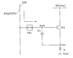
도 1a 내지 1f는 도 7과의 대비로서 본 발명의 실시예 1의 디스플레이 장치에 있어서의 화소회로의 구동을 나타내는 타임 차트다. 본 실시예 1의 디스플레이 장치는, 도 1a에 나타내는 기록신호 WS를 라이트 스캔 회로(24A)가 생성해서 화소(23)를 구동하는 점을 제외하고 상기의 디스플레이 장치와 동일하게 구성된다.1A to 1F are time charts showing driving of a pixel circuit in the display device of
실시예 1의 디스플레이 장치의 라이트 스캔 회로(24A)는, 유기EL소자(8)의 발광을 정지시키는 비발광 기간 내이며, 화소(23)의 구동에 아무런 영향을 주지 않는 기간 T 동안, 기간 T를 제외한 다른 기간에 있어서 기간이 짧은 측의 신호레벨로 기록신호의 신호레벨을 설정한다. 따라서 도 1a 내지 1f에 나타낸 실시예 1에서는, 비발광 기간이 시작되어 신호레벨 유지용 콘덴서 C1의 축적 전하를 방전시킨 후, 임계값전압의 보정을 시작하기 직전까지의 기간 T 동안(도 9 참조), 기록신호 WS를 H레벨로 유지한다. 이 때 도 1a 내지 1f에서는, 도 7a 내지 7e의 기록신호 WS를 도 1a 내지 1f와의 대비를 위해 파선으로 나타낸다.The
(2) 실시예 1의 동작(2) Operation of Example 1
이상의 구성에 있어서, 실시예 1의 디스플레이 장치에서는(도 6∼도 15 참조), 수평구동회로 및 수직구동회로에 의해 신호선 SIG 및 주사선 SCN을 순차 라인 단위로 구동하여, 표시부(22)의 화소(23)에 신호선 SIG의 신호레벨 Vsig를 각각 설정한다. 또한, 이렇게 설정된 신호레벨 Vsig에 의해 각 화소(23)의 유기EL소자(8)가 발광하고, 원하는 화상이 표시부(22)에 표시된다.In the above configuration, in the display device of the first embodiment (see FIGS. 6 to 15), the horizontal line circuit and the vertical line drive circuit drive the signal line SIW and the scan line SCN in sequential line units, so that the pixels of the display unit 22 ( In 23), the signal level Vsig of the signal line SIV is set, respectively. In addition, the
즉, 실시예 1의 디스플레이 장치에서는, 비발광 기간에, 이 신호레벨 유지용 콘덴서 C1의 일단이 신호선 SIG의 신호레벨 Vsig로 세트된다. 반면, 발광 기간에, 이 신호레벨 유지용 콘덴서 C1의 단자간 전압에 의한 게이트 소스간 전압 Vgs에 의해, 트랜지스터 TR2에 의해 유기EL소자(8)가 구동된다. 그 결과, 실시예 1의 디스플레이 장치에서는, 신호선 SIG의 신호레벨 Vsig에 따른 발광 휘도로 각 화소(23)의 유기EL소자(8)가 발광한다.That is, in the display device of Example 1, one end of the signal level holding capacitor C1 is set to the signal level susig of the signal line SIg in the non-luminescing period. On the other hand, in the light emitting period, the
실시예 1의 디스플레이 장치에서는, 이 비발광 기간에, 우선 신호레벨 유지용 콘덴서 C1의 양단 전압이 소정의 고정 전위 Vofs 및 Vss로 설정된다. 그 후, 유기EL소자(8)를 구동하는 트랜지스터 TR2를 통한 방전에 의해, 신호레벨 유지용 콘덴서 C1에 트랜지스터 TR2의 임계값전압 Vth가 설정된다(도 7a 내지 7e, 기간 Tth1, Tth2, T th3). 이에 따라 트랜지스터 TR2의 임계값전압 Vth의 편차에 의한 발광 휘도의 편차가 보정된다.In the display device of the first embodiment, the voltage at both ends of the signal level holding capacitor C1 is first set to the predetermined fixed potentials Vs and Vss in this non-luminescing period. Thereafter, the threshold voltage Vt is set by the transistor Tr2 to the signal level holding capacitor C1 by the discharge through the transistor Tr2 driving the organic EL element 8 (Figs. 7A to 7E, the periods T1, T2, T2, T2). ). As a result, the variation in the light emission luminance due to the variation in the threshold voltage St2 of the transistor TR2 is corrected.
또 그 후에 기록신호 WS에 의해 트랜지스터 TR1을 온 상태로 설정하여, 신호레벨 유지용 콘덴서 C1의 신호선 SIG측단을 신호선 SIG에 접속한다. 이 상태에서, 트랜지스터 TR2를 온 동작시켜서 신호레벨 유지용 콘덴서 C1의 타단을 충전한다.(도 7a 내지 7e, 기간 Tμ). 이에 따라 트랜지스터 TR2의 이동도의 편차에 의한 발광 휘도의 편차가 보정된다.After that, the transistor TR1 is set to the ON state by the write signal WS, and the signal line SI 'side end of the signal level holding capacitor C1 is connected to the signal line SI'. In this state, the transistor TR2 is turned on to charge the other end of the capacitor C1 for maintaining the signal level (Figs. 7A to 7E, period T mu). Thereby, the deviation of the luminescence brightness due to the variation in the mobility of the transistor Tr2 is corrected.
실시예 1의 디스플레이 장치에서는, 일정 기간의 경과 후에, 기록신호 WS에 의해 트랜지스터 TR2가 온 상태에서 오프 상태로 전환된다. 이에 따라 신호레벨 유지용 콘덴서 C1에 신호선 SIG의 신호레벨 Vsig가 샘플 홀드 되고, 유기EL소자(8)의 발광 휘도가 설정된다.In the display device of the first embodiment, after a certain period of time, the transistor TRS2 is switched from the on state to the off state by the write signal WS. As a result, the signal level Vig of the signal line SIV is sampled and held in the signal level holding capacitor C1, and the light emission luminance of the
이에 따라 실시예 1의 디스플레이 장치에서는, 신호레벨 유지용 콘덴서 C1을 신호선 SIG에 접속하는 트랜지스터 TR1에 있어서, 임계값전압 Vth가 변화하면, 트랜지스터 TR2의 이동도를 보정하는 기간 Tμ가 변화한다. 또한, 이동도의 편차를 과대하게 보정함에 따라, 화질이 열화하고, 계조를 설정할 수 없게 된다.Accordingly, in the display device of the first embodiment, in the transistor Tr1 connecting the signal level holding capacitor C1 to the signal line SIw, when the threshold voltage Vt is changed, the period T mu of correcting the mobility of the transistor Tr2 changes. In addition, as the deviation in mobility is excessively corrected, the image quality deteriorates and the gray level cannot be set.
한편, 트랜지스터 TR1, TR2를 구성하는 폴리실리콘 TFT, 또는 아모포스 트랜지스터에서는, 소스 전압 Vs에 대한 게이트 전압 Vg에 따라 임계값전압 Vth가 경시 변화된다(도 16 및 도 17). 따라서 단지 신호레벨 유지용 콘덴서 C1의 단자간 전압을 트랜지스터 TR1의 임계값전압 Vth로 설정하는 기간 Tth1, Tth2, Tth3 동안, 이동도를 보정하는 기간 Tμ 동안에만, 기록신호 WS의 신호레벨을 상승시키면, 기록신호 WS의 출력 대상인 트랜지스터 TR1에 있어서, 임계값전압 Vth가 시간에 따른 변화에 의해 저하하고, 이동도를 보정하는 기간 Tμ이 서서히 증대하는 방향으로 변화한다. 그 결과, 화질이 열화하고, 계조를 설정할 수 없게 된다.On the other hand, in the polysilicon TFTs or amorphous transistors constituting the transistors Tr1 and Tr2, the threshold voltage Vtyl is changed over time according to the gate voltage Vsg with respect to the source voltage Vs (Figs. 16 and 17). Therefore, if the signal level of the recording signal PSS is increased only during the period Tμ during which the voltage between the terminals of the signal level holding capacitor C1 is set to the threshold voltage voltage of the transistor TrT1, T2, and T3, the mobility is corrected. In the transistor Tr1, which is the output target of the write signal WS, the threshold voltage Vt is lowered with the change over time, and the period T μ during which the mobility is corrected is gradually changed. As a result, the image quality deteriorates, and the gray level cannot be set.
이상을 고려하여 실시예 1에서는, 유기EL소자(8)의 발광을 정지시키는 비발광 기간 내이며, 유기EL소자(8)의 구동에 아무런 영향을 주지 않는 기간(도 1a 내지 1f) 동안, 기간(T)을 제외한 다른 기간에 있어서 기간이 짧은 측의 신호레벨로 설정된다. 즉 이 경우, 도 1a 내지 1f에 있어서 기간 T 동안, 기록신호 WS의 신호레벨이 H레벨로 설정된다.In view of the above, in Example 1, it is within the non-light emission period which stops light emission of the
이에 따라 실시예 1의 디스플레이 장치에서는, 단지 신호레벨 유지용 콘덴서 C1의 단자간 전압을 트랜지스터 TR1의 임계값전압 Vth로 설정하는 기간 Tth1, Tth2, Tth3 동안, 이동도를 보정하는 기간 Tμ 동안에만, 기록신호 WS의 신호레벨을 상승시킬 경우에 비해, 보다 긴 기간 동안, 기록신호 WS의 신호레벨을 상승시킬 수 있다. 따라서 기록신호 WS에 있어서의 신호레벨의 기울기를 줄일 수 있다. 따라서 종래에 비해서 시간에 따른 변화에 의한 기록용 트랜지스터에 있어서의 임계값전압의 변화를 방지할 수 있다. 그 결과, 임계값전압의 변화에 기인하는 시간에 따른 변화에 의한 화질의 열화, 계조를 설정할 수 없게 되는 현상을 효과적으로 회피할 수 있다.Accordingly, in the display device of the first embodiment, only during the period Tμ during the period in which the terminal-to-terminal voltage of the signal level holding capacitor C1 is set to the threshold voltage voltage of the transistor TrT1, T2, and T3, during the period Tμ for correcting mobility In comparison with the case where the signal level of the recording signal is increased, the signal level of the recording signal is increased for a longer period. Therefore, the slope of the signal level in the recording signal WS can be reduced. Therefore, it is possible to prevent the change of the threshold voltage in the write transistor due to the change over time compared with the prior art. As a result, it is possible to effectively avoid the phenomenon of deterioration of image quality and the inability to set the gray scale due to the change over time due to the change in the threshold voltage.
여기에서 유기EL소자(8)의 화소에서는, 기록신호 WS의 H레벨은 30V 정도이고, 기록신호 WS의 L레벨은 -3V 정도이다. 한편, 시간에 따른 변화에 의한 임계값전압 Vth의 변화는, 게이트 소스간 전압의 극성뿐만 아니라, 전압값에 의해서도 변화되는 특징이 있다.Here, in the pixel of the
이에 따라 이러한 기록신호 WS에 있어서의 신호레벨의 기울기에 의한 트랜지스터 TR1의 임계값전압 Vth의 시간에 따른 변화는, 기록신호 WS에 있어서 의 신호레벨의 기울기를 완전히 없앴을 경우, 즉 기록신호 WS에 있어서, 신호레벨이 상승하는 기간과, 신호레벨이 하강하는 기간을 거의 동일하게 했을 경우에, 완전히 방지할 수 있다고 생각된다. 그러나 실시예 1과 같이, 여전히 기울기가 남아있는 경우에도, 트랜지스터 TR1의 임계값전압 Vth의 시간에 따른 변화를 실용상 충분히 방지할 수 있다.Accordingly, the change over time of the threshold voltage Vt of the transistor Tr1 due to the slope of the signal level in the write signal VS is completely eliminated from the slope of the signal level in the write signal VS, that is, in the write signal GS. Therefore, it is considered that the period can be completely prevented when the period during which the signal level rises and the period during which the signal level falls are substantially the same. However, as in the first embodiment, even when the slope still remains, the change over time of the threshold voltage Styl of the transistor Tr1 can be sufficiently prevented in practical use.
이에 따라 실시예 1과 같이, 기록신호 WS에 있어서, L레벨로 유지되는 기간에 비해서 H레벨로 유지되는 기간이 여전히 짧은 경우에도, 실용상 충분하게, 임계값전압 Vth의 시간에 따른 변화를 방지할 수 있다.Accordingly, as in the first embodiment, even in a case where the period of time maintained at the H level is still short compared to the period maintained at the L level, the change over time of the threshold voltage Vt is sufficiently prevented in practical use. can do.
(3) 실시예 1의 효과(3) Effect of Example 1
본 발명의 실시예 1에 의하면, 발광소자의 발광을 정지시키는 비발광 기간 내이며, 발광소자의 구동에 아무런 영향을 주지 않는 기간의 전부 기간 동안, 다른 기간에 있어서 기간이 짧은 측의 신호레벨에 기록신호의 신호레벨을 설정한다. 그 결과, 임계값전압의 변화에 기인하는 시간에 따른 변화에 의한 화질의 열화, 계조를 설정할 수 없게 되는 현상을 효과적으로 회피할 수 있다.According to the first embodiment of the present invention, in the non-light emitting period in which light emission of the light emitting element is stopped, and for all the periods in which there is no influence on the driving of the light emitting element, the signal level of the shorter period in the other period is Set the signal level of the recording signal. As a result, it is possible to effectively avoid the phenomenon of deterioration of image quality and the inability to set the gray scale due to the change over time due to the change in the threshold voltage.
즉, 기록신호의 신호레벨의 설정에 의해, 기록용 트랜지스터에 있어서의 임계값전압의 변화를 보정함으로써, 임계값전압의 변화에 기인하는 시간에 따른 변화에 의한 화질의 열화, 계조를 설정할 수 없게 되는 현상을 효과적으로 회피할 수 있다.In other words, by setting the signal level of the recording signal, the change of the threshold voltage in the recording transistor is corrected, whereby deterioration of image quality and the gray scale due to the change over time due to the change of the threshold voltage cannot be set. This phenomenon can be effectively avoided.
또 각 화소에 있어서, 신호레벨 유지용 콘덴서에 구동용 트랜지스터의 임계값전압을 설정하여, 임계값전압의 편차에 의한 발광 휘도를 방지함으로써, 고화질 의 표시 화상을 얻을 수 있다.In each pixel, by setting the threshold voltage of the driving transistor in the signal level holding capacitor and preventing the light emission luminance due to the deviation of the threshold voltage, a high quality display image can be obtained.
또 구동용 트랜지스터를 온 동작시켜서 신호레벨 유지용 콘덴서의 타단을 충전하고, 구동용 트랜지스터의 이동도의 편차를 보정하고, 구동용 트랜지스터의 이동도의 편차에 의한 발광소자의 발광 휘도의 편차를 방지한다. 그 결과, 고화질의 표시 화상을 얻을 수 있다. 또 구동용 트랜지스터의 임계값전압 Vth의 변화에 의한, 이동도의 편차를 보정하는 기간의 변화를 방지할 수 있다. 그 결과, 고화질의 표시 화상을 얻을 수 있다.Further, the driving transistor is turned on to charge the other end of the signal level holding capacitor, to correct the variation in the mobility of the driving transistor, and to prevent the variation in the light emission luminance of the light emitting element due to the variation in the mobility of the driving transistor. do. As a result, a high quality display image can be obtained. In addition, it is possible to prevent a change in the period for correcting the variation in mobility due to the change in the threshold voltage Vt of the driving transistor. As a result, a high quality display image can be obtained.
[실시예 2]Example 2
이 때 상기의 실시예 1에 있어서는, 비발광 기간 내의 발광소자의 구동에 아무런 영향을 주지 않는 기간의 전부 기간에, 다른 기간에 있어서 기간이 짧은 측의 신호레벨로 기록신호의 신호레벨을 설정할 경우에 대해서 서술했지만, 본 발명은 이에 한정되지 않는다. 즉, 기록용 트랜지스터에 있어서의 임계값전압의 시간에 따른 변화를 지나치게 보정할 경우 등에는, 비발광 기간 내의 발광소자의 구동에 아무런 영향을 주지 않는 기간의 일부 기간에, 기간이 짧은 측의 신호레벨로 기록신호의 신호레벨을 설정해도 좋다.At this time, in the first embodiment, when the signal level of the recording signal is set to the signal level on the shorter side in another period in all the periods during which the driving of the light emitting element in the non-light emitting period has no effect. Although it demonstrated, this invention is not limited to this. That is, in the case where the change in the threshold voltage over time in the recording transistor is excessively corrected, for example, a signal on the side having a shorter period in a part of the period during which the driving of the light emitting element in the non-light emitting period has no effect. The signal level of the recording signal may be set at the level.
또 상기의 실시예 1에서는, 도 6의 회로 구성에 의한 화소회로를 도 7a 내지 7e에 나타내는 타이밍에 의해 구동할 경우에 대해서 서술했지만, 본 발명은 이에 한정하지 않는다. 즉, 본 발명은 각종 회로 구성에 의해 화소를 구성할 경우, 또한 여러 가지 타이밍으로 화소를 구동할 경우 등에도 널리 적용할 수 있다.In the first embodiment, the case where the pixel circuit having the circuit configuration of FIG. 6 is driven at the timing shown in FIGS. 7A to 7E has been described. However, the present invention is not limited thereto. That is, the present invention can be widely applied to the case of constituting the pixel by various circuit configurations, and to driving the pixel at various timings.
또 상기의 실시예 1에서는, 각 트랜지스터를 폴리실리콘 TFT로 구성할 경 우에 대해서 서술했지만, 본 발명은 이에 한정하지 않는다. 즉, 본 발명은 각 트랜지스터를 각종 트랜지스터로 구성할 경우에도 널리 적용할 수 있다.In addition, in Example 1 mentioned above, the case where each transistor is comprised by polysilicon TFT is demonstrated, but this invention is not limited to this. That is, the present invention can be widely applied to the case where each transistor is composed of various transistors.
또 상기의 실시예 1에서는, N채널형 트랜지스터를 통해 신호레벨 유지용 콘덴서를 신호선에 접속할 경우에 대해서 서술했지만, 본 발명은 이에 한정하지 않는다. 즉, 본 발명은 P채널형 트랜지스터를 통해 신호레벨 유지용 콘덴서를 신호선에 접속할 경우에도 널리 적용할 수 있다.In the first embodiment, the case where the signal level holding capacitor is connected to the signal line through the N-channel transistor is described. However, the present invention is not limited thereto. That is, the present invention can be widely applied to the case where a capacitor for maintaining a signal level is connected to a signal line through a P-channel transistor.
또 상기의 실시예 1에서는, 발광소자에 유기EL소자를 사용할 경우에 대해서 서술했지만, 본 발명은 이에 한정되지 않는다. 즉, 본 발명은 발광소자에 전류구동형의 각종 발광소자를 사용할 경우에도 널리 적용할 수 있다.In addition, in Example 1 mentioned above, the case where an organic EL element is used for a light emitting element was described, but this invention is not limited to this. That is, the present invention can be widely applied to the case of using a variety of light emitting devices of the current driving type in the light emitting device.
본 발명은, 예를 들면 폴리실리콘 TFT를 사용한 유기EL소자에 의한 액티브 매트릭스형 디스플레이 장치에 적용할 수 있다.The present invention can be applied to, for example, an active matrix display device using an organic EL element using polysilicon TFT.
도 1a 내지 1f는 본 발명의 실시예 1에 있어서의 디스플레이 장치의 각 화소의 구동의 설명에 제공하는 타임 차트다.1A to 1F are time charts for explaining the driving of each pixel of the display device according to the first embodiment of the present invention.
도 2는 종래의 디스플레이 장치를 나타내는 블럭도다.2 is a block diagram showing a conventional display device.
도 3은 도 2에 나타낸 디스플레이 장치로서 회로를 부분적으로 나타내는 블럭도다.FIG. 3 is a block diagram partially showing a circuit as the display device shown in FIG. 2.
도 4는 도 3에 나타낸 유기EL소자의 시간에 따른 변화를 나타내는 특성 곡선도다.FIG. 4 is a characteristic curve diagram showing changes with time of the organic EL element shown in FIG. 3.
도 5는 도 3에 나타낸 디스플레이 장치의 구성에 N채널형 트랜지스터를 사용했을 경우로서 회로를 부분적으로 나타내는 블럭도다.FIG. 5 is a block diagram partially showing a circuit when an N-channel transistor is used in the configuration of the display device shown in FIG. 3.
도 6은 N채널형 트랜지스터를 사용해서 상정되는 디스플레이 장치를 나타내는, 회로를 부분적으로 나타내는 블럭도다.Fig. 6 is a block diagram partially showing a circuit showing a display device assumed using an N-channel transistor.
도 7a 내지 7e는 도 6에 나타낸 디스플레이 장치의 동작을 설명하는 타임 차트다.7A to 7E are time charts illustrating the operation of the display device shown in FIG. 6.
도 8은 도 7a 내지 7e에 나타낸 발광 기간에 있어서 화소의 설정에 대한 접속 상태를 나타내는 회로도다.FIG. 8 is a circuit diagram showing a connection state with respect to setting of pixels in the light emission period shown in FIGS. 7A to 7E.
도 9는 도 8에 나타낸 접속 상태에 이어지는 접속 상태를 나타내는 회로도다.FIG. 9 is a circuit diagram showing a connection state following the connection state shown in FIG. 8.
도 10은 도 9에 나타낸 접속 상태에 이어지는 접속 상태를 나타내는 회로도다.FIG. 10 is a circuit diagram showing a connection state following the connection state shown in FIG. 9.
도 11은 도 10에 나타낸 접속 상태에 이어지는 접속 상태를 나타내는 회로도다.FIG. 11 is a circuit diagram illustrating a connection state following the connection state shown in FIG. 10.
도 12는 N채널형 트랜지스터의 임계값전압의 보정의 설명에 제공하는 특성 곡선도다.12 is a characteristic curve diagram for explaining the correction of the threshold voltage of an N-channel transistor.
도 13은 도 11에 나타낸 접속 상태에 이어지는 접속 상태를 나타내는 회로도다.FIG. 13 is a circuit diagram showing a connection state following the connection state shown in FIG. 11.
도 14는 도 13에 나타낸 접속 상태에 이어지는 접속 상태를 나타내는 회로도다.FIG. 14 is a circuit diagram illustrating a connection state following the connection state shown in FIG. 13.
도 15는 N채널형 트랜지스터의 이동도의 보정의 설명에 제공하는 특성 곡선도다.15 is a characteristic curve diagram for explaining correction of mobility of an N-channel transistor.
도 16은 N채널형 트랜지스터의 임계값전압의 시간에 따른 변화의 설명에 제공하는 특성 곡선도다.Fig. 16 is a characteristic curve diagram for explaining the change over time of the threshold voltage of an N-channel transistor.
도 17은 도 16과는 반대의 극성에 의한 N채널형 트랜지스터의 임계값전압의 시간에 따른 변화의 설명에 제공하는 특성 곡선도다.FIG. 17 is a characteristic curve diagram for explaining the change over time of the threshold voltage of an N-channel transistor due to the polarity opposite to that of FIG. 16.
도 18은 N채널형 트랜지스터의 임계값전압의 시간에 따른 변화에 의한 이동도의 편차 보정에의 영향을 나타내는 타임 차트다.Fig. 18 is a time chart showing the influence of the deviation correction of mobility due to the change of the threshold voltage of the N-channel transistor with time.
Claims (5)
Applications Claiming Priority (2)
| Application Number | Priority Date | Filing Date | Title |
|---|---|---|---|
| JPJP-P-2007-00197081 | 2007-07-30 | ||
| JP2007197081A JP2009031620A (en) | 2007-07-30 | 2007-07-30 | Display device and driving method of display device |
Publications (1)
| Publication Number | Publication Date |
|---|---|
| KR20090013027A true KR20090013027A (en) | 2009-02-04 |
Family
ID=40331883
Family Applications (1)
| Application Number | Title | Priority Date | Filing Date |
|---|---|---|---|
| KR1020080063339A KR20090013027A (en) | 2007-07-30 | 2008-07-01 | Display device and method of driving the same |
Country Status (5)
| Country | Link |
|---|---|
| US (1) | US8519919B2 (en) |
| JP (1) | JP2009031620A (en) |
| KR (1) | KR20090013027A (en) |
| CN (1) | CN101359448B (en) |
| TW (1) | TW200912853A (en) |
Families Citing this family (3)
| Publication number | Priority date | Publication date | Assignee | Title |
|---|---|---|---|---|
| JP2010281914A (en) * | 2009-06-03 | 2010-12-16 | Sony Corp | Display, method for driving display, and electronic device |
| CN110893159B (en) * | 2019-12-03 | 2022-05-27 | 山东中医药大学 | Traditional Chinese medicine mask with heat-clearing and detoxifying effects and preparation method thereof |
| US11875755B2 (en) | 2022-01-14 | 2024-01-16 | Samsung Electronics Co., Ltd. | Method of driving light emitting diode backlight unit and display device performing the same |
Family Cites Families (25)
| Publication number | Priority date | Publication date | Assignee | Title |
|---|---|---|---|---|
| US5684365A (en) | 1994-12-14 | 1997-11-04 | Eastman Kodak Company | TFT-el display panel using organic electroluminescent media |
| TW554558B (en) * | 2001-07-16 | 2003-09-21 | Semiconductor Energy Lab | Light emitting device |
| JP3613253B2 (en) * | 2002-03-14 | 2005-01-26 | 日本電気株式会社 | Current control element drive circuit and image display device |
| JP2004118132A (en) * | 2002-09-30 | 2004-04-15 | Hitachi Ltd | Direct-current driven display device |
| US7612749B2 (en) * | 2003-03-04 | 2009-11-03 | Chi Mei Optoelectronics Corporation | Driving circuits for displays |
| JP4049018B2 (en) * | 2003-05-19 | 2008-02-20 | ソニー株式会社 | Pixel circuit, display device, and driving method of pixel circuit |
| JP4049037B2 (en) * | 2003-06-30 | 2008-02-20 | ソニー株式会社 | Display device and driving method thereof |
| JP2005099715A (en) * | 2003-08-29 | 2005-04-14 | Seiko Epson Corp | Driving method of electronic circuit, electronic circuit, electronic device, electrooptical device, electronic equipment and driving method of electronic device |
| JP4131227B2 (en) * | 2003-11-10 | 2008-08-13 | ソニー株式会社 | Pixel circuit, display device, and driving method of pixel circuit |
| US7173590B2 (en) * | 2004-06-02 | 2007-02-06 | Sony Corporation | Pixel circuit, active matrix apparatus and display apparatus |
| JP5017773B2 (en) * | 2004-09-17 | 2012-09-05 | ソニー株式会社 | Pixel circuit, display device, and driving method thereof |
| JP4850422B2 (en) * | 2005-01-31 | 2012-01-11 | パイオニア株式会社 | Display device and driving method thereof |
| JP4923410B2 (en) * | 2005-02-02 | 2012-04-25 | ソニー株式会社 | Pixel circuit and display device |
| JP4752331B2 (en) * | 2005-05-25 | 2011-08-17 | セイコーエプソン株式会社 | Light emitting device, driving method and driving circuit thereof, and electronic apparatus |
| JP2007108381A (en) * | 2005-10-13 | 2007-04-26 | Sony Corp | Display device and driving method of same |
| US8004477B2 (en) * | 2005-11-14 | 2011-08-23 | Sony Corporation | Display apparatus and driving method thereof |
| JP5245195B2 (en) * | 2005-11-14 | 2013-07-24 | ソニー株式会社 | Pixel circuit |
| JP4240059B2 (en) * | 2006-05-22 | 2009-03-18 | ソニー株式会社 | Display device and driving method thereof |
| JP2007316454A (en) * | 2006-05-29 | 2007-12-06 | Sony Corp | Image display device |
| JP4151714B2 (en) * | 2006-07-19 | 2008-09-17 | ソニー株式会社 | Display device and driving method thereof |
| JP4203772B2 (en) * | 2006-08-01 | 2009-01-07 | ソニー株式会社 | Display device and driving method thereof |
| JP5055963B2 (en) * | 2006-11-13 | 2012-10-24 | ソニー株式会社 | Display device and driving method of display device |
| JP2008203478A (en) * | 2007-02-20 | 2008-09-04 | Sony Corp | Display device and driving method thereof |
| JP2008233129A (en) * | 2007-03-16 | 2008-10-02 | Sony Corp | Pixel circuit, display device and driving method of pixel circuit |
| JP4293262B2 (en) * | 2007-04-09 | 2009-07-08 | ソニー株式会社 | Display device, display device driving method, and electronic apparatus |
-
2007
- 2007-07-30 JP JP2007197081A patent/JP2009031620A/en active Pending
-
2008
- 2008-06-24 TW TW097123532A patent/TW200912853A/en unknown
- 2008-06-30 US US12/216,082 patent/US8519919B2/en active Active
- 2008-07-01 KR KR1020080063339A patent/KR20090013027A/en not_active Application Discontinuation
- 2008-07-30 CN CN2008101311394A patent/CN101359448B/en active Active
Also Published As
| Publication number | Publication date |
|---|---|
| US8519919B2 (en) | 2013-08-27 |
| JP2009031620A (en) | 2009-02-12 |
| TW200912853A (en) | 2009-03-16 |
| CN101359448B (en) | 2011-01-12 |
| CN101359448A (en) | 2009-02-04 |
| US20090033652A1 (en) | 2009-02-05 |
Similar Documents
| Publication | Publication Date | Title |
|---|---|---|
| US9466243B2 (en) | Compensation of threshold voltage in driving transistor of organic light emitting diode display device | |
| US8471838B2 (en) | Pixel circuit having a light detection element, display apparatus, and driving method for correcting threshold and mobility for light detection element of pixel circuit | |
| JP5023906B2 (en) | Display device and driving method of display device | |
| JP4300492B2 (en) | Display device | |
| JP4983018B2 (en) | Display device and driving method thereof | |
| JP4300491B2 (en) | Display device | |
| JP4967946B2 (en) | Display device and driving method of display device | |
| KR20070041378A (en) | Display and method for driving display | |
| KR20100064940A (en) | Display device and driving method thereof | |
| JP4826598B2 (en) | Image display device and driving method of image display device | |
| KR20080084730A (en) | Pixel circuit, display device, and driving method thereof | |
| KR101589901B1 (en) | Image display device and method of driving the same | |
| KR101892307B1 (en) | Driving method of display apparatus | |
| KR20080087721A (en) | Display apparatus, display-apparatus driving method and electronic equipment | |
| KR101581959B1 (en) | Image display apparatus and method of driving the image display apparatus | |
| JP4281019B2 (en) | Display device | |
| US8866718B2 (en) | Drive circuit and display device | |
| JP2008224787A (en) | Display device and driving method of display device | |
| US8610647B2 (en) | Image display apparatus and method of driving the image display apparatus | |
| KR20100039250A (en) | Display apparatus and display driving method | |
| US20100259532A1 (en) | Display device and display driving method | |
| US10482814B2 (en) | Display device and method for driving same | |
| JP4281018B2 (en) | Display device | |
| KR20090013027A (en) | Display device and method of driving the same | |
| JP4687026B2 (en) | Display device and driving method of display device |
Legal Events
| Date | Code | Title | Description |
|---|---|---|---|
| WITN | Application deemed withdrawn, e.g. because no request for examination was filed or no examination fee was paid |